CN103151355A - Semiconductor memory device - Google Patents
Semiconductor memory deviceDownload PDFInfo
- Publication number
- CN103151355A CN103151355ACN2012104871712ACN201210487171ACN103151355ACN 103151355 ACN103151355 ACN 103151355ACN 2012104871712 ACN2012104871712 ACN 2012104871712ACN 201210487171 ACN201210487171 ACN 201210487171ACN 103151355 ACN103151355 ACN 103151355A
- Authority
- CN
- China
- Prior art keywords
- potential
- node
- transistor
- resistance
- semiconductor memory
- Prior art date
- Legal status (The legal status is an assumption and is not a legal conclusion. Google has not performed a legal analysis and makes no representation as to the accuracy of the status listed.)
- Pending
Links
Images


Classifications
- G—PHYSICS
- G11—INFORMATION STORAGE
- G11C—STATIC STORES
- G11C11/00—Digital stores characterised by the use of particular electric or magnetic storage elements; Storage elements therefor
- G11C11/21—Digital stores characterised by the use of particular electric or magnetic storage elements; Storage elements therefor using electric elements
- G—PHYSICS
- G11—INFORMATION STORAGE
- G11C—STATIC STORES
- G11C14/00—Digital stores characterised by arrangements of cells having volatile and non-volatile storage properties for back-up when the power is down
- G11C14/0054—Digital stores characterised by arrangements of cells having volatile and non-volatile storage properties for back-up when the power is down in which the volatile element is a SRAM cell
- G11C14/009—Digital stores characterised by arrangements of cells having volatile and non-volatile storage properties for back-up when the power is down in which the volatile element is a SRAM cell and the nonvolatile element is a resistive RAM element, i.e. programmable resistors, e.g. formed of phase change or chalcogenide material
Landscapes
- Engineering & Computer Science (AREA)
- Computer Hardware Design (AREA)
- Semiconductor Memories (AREA)
- Static Random-Access Memory (AREA)
Abstract
Translated fromChinese
Description
Translated fromChinese相关专利申请的交叉引用Cross references to related patent applications
2011年11月25日提交的日本专利申请No.2011-257063的公开,包括说明书、附图和摘要的全部内容以引用方式并入本文。The disclosure of Japanese Patent Application No. 2011-257063 filed on Nov. 25, 2011, including specification, drawings and abstract, is incorporated herein by reference in its entirety.
技术领域technical field
本发明涉及半导体存储器件,更具体地,涉及当应用到包括SRAM的半导体存储器件时有效的技术。The present invention relates to semiconductor memory devices, and more particularly, to techniques that are effective when applied to semiconductor memory devices including SRAMs.
背景技术Background technique
SRAM(静态随机存取存储器)是一种半导体器件,其通过使用触发器存储数据。例如,在SRAM中,数据(“1”或“0”)被存储在由四个晶体管构成的、两个交叉耦合的CMOS反相器中。因为为了读取和写入存取,额外需要两个晶体管,所以由六个晶体管构成典型SRAM的存储单元。SRAM (Static Random Access Memory) is a semiconductor device that stores data by using flip-flops. For example, in SRAM, data (“1” or “0”) is stored in two cross-coupled CMOS inverters made of four transistors. Since two additional transistors are required for read and write access, the memory cell of a typical SRAM is made up of six transistors.
例如,以下引用的专利文献1(PCT国际公开No.2006-527897的公开日语译文)公开了一种非易失性静态存储单元,其中,非易失性单元(14、16)交叉耦合到静态存储单元的内部节点(A、B)。两个非易失性单元中的一个非易失性单元(14)具有与B耦合的控制栅极和与A耦合的源极,并且另一个非易失性单元(16)具有与A耦合的控制栅极和与B耦合的源极。For example, Patent Document 1 (published Japanese translation of PCT International Publication No. 2006-527897) cited below discloses a non-volatile static memory unit in which non-volatile units (14, 16) are cross-coupled to static Internal nodes (A, B) of the storage unit. One of the two nonvolatile cells (14) has a control gate coupled to B and a source coupled to A, and the other nonvolatile cell (16) has a Control gate and source coupled to B.
以下引用的专利文献2(公开的日本未经审查的专利申请No.平7(1995)-226088)公开了一种半导体存储器件,其可以实现非易失性特性同时维持静态存储器(SRAM)的高速。这种半导体存储器件具有SRAM存储单元1和非易失性存储单元3。SRAM存储单元1是通过将第一选择晶体管T7和第二选择晶体管T8耦合到两个晶体管T1和T2来构成的,这两个晶体管T1和T2各自的源极接地并且各自的漏极耦合到彼此的栅极。非易失性存储单元3由非易失性晶体管T3和T4构成,非易失性晶体管T3和T4设置有两个栅极:悬浮栅极和控制栅极,以及与电源线耦合的漏极,从而存储SRAM存储单元1的状态。Patent Document 2 (Published Japanese Unexamined Patent Application No. Hei 7(1995)-226088) cited below discloses a semiconductor memory device that can achieve non-volatile characteristics while maintaining static memory (SRAM) high speed. This semiconductor memory device has an
专利文献3(PCT国际公开No.2003-511809的公开日语译文)公开了一种非易失性MOSRAM单元,其由第一和第二反相器以及电容器(G1、G2)构成,电容器(G1、G2)每个都串联耦合到第一和第二反相器中的每一个的控制电极。Patent Document 3 (published Japanese translation of PCT International Publication No. 2003-511809) discloses a nonvolatile MOSRAM cell composed of first and second inverters and capacitors (G1, G2), the capacitor (G1 , G2) are each coupled in series to the control electrode of each of the first and second inverters.
以下引用的专利文献4(公开的日本未经审查的专利申请No.2007-157183)公开了一种非易失性存储器,其由触发器构成,该触发器包括以静态锁存模式耦合的一对负载晶体管和存储器静态的串联电路。这个非易失性存储器设置有漏电流截止元件(T16、T26),漏电流截止元件(T16、T26)耦合在写入和擦除时漏电流经由负载晶体管流入触发器电源侧所经过的电流路径。Patent Document 4 (Published Japanese Unexamined Patent Application No. 2007-157183) cited below discloses a nonvolatile memory consisting of a flip-flop including a Static series circuit for load transistor and memory. This non-volatile memory is provided with a leakage current cut-off element (T16, T26) that couples the current path through which the leakage current flows into the power supply side of the flip-flop through the load transistor during writing and erasing .
以下引用的专利文献5(公开的日本未经审查的专利申请No.平6(1994)-76582)公开了一种非易失性存储器,其通过改变用作存储单元的一对触发器的场效应晶体管(RMmn(o+)、RMmn(o-))的阈值电压来存储信息。Patent Document 5 (Published Japanese Unexamined Patent Application No. Hei 6(1994)-76582) cited below discloses a nonvolatile memory which, by changing the field of a pair of flip-flops used as memory cells, The threshold voltage of the effect transistor (RMmn(o+), RMmn(o-)) is used to store information.
以下引用的专利文献6(公开的日本未经审查的专利申请No.平7(1995)-183401)公开了一种非易失性存储器,其包括作为负载元件的四个N沟道MOS晶体管和两个P沟道TFT。TFT具有层叠结构,该层叠结构由下层的第一TFT栅电极9、TFT栅极绝缘膜10、形成TFT的沟道的主体层(半导体层)13、具有铁电性的第二栅极绝缘膜22和第二TFT栅电极23组成。Patent Document 6 cited below (Published Japanese Unexamined Patent Application No. Hei 7(1995)-183401) discloses a nonvolatile memory including four N-channel MOS transistors as load elements and Two P-channel TFTs. The TFT has a stacked structure consisting of the lower first TFT gate electrode 9, the TFT
以下引用的专利文献7(公开的日本未经审查的专利申请No.2004-207282)公开了一种非易失性SRAM单元,其包括一对的两个交叉耦合的CMOS反相器c1和c2和铁电电容器fc1和fc2。铁电电容器fc1和fc2分别由下电极BEL1和BLE2、铁电膜FER1和FER2和上电极TEL1和TEL2形成,下电极BEL1和BLE2分别耦合到包括在两个CMOS反相器中的对应的反相器中的漏极扩散区。Patent Document 7 (Published Japanese Unexamined Patent Application No. 2004-207282) cited below discloses a nonvolatile SRAM cell comprising a pair of two cross-coupled CMOS inverters c1 and c2 and ferroelectric capacitors fc1 and fc2. Ferroelectric capacitors fc1 and fc2 are formed by lower electrodes BEL1 and BLE2, ferroelectric films FER1 and FER2, and upper electrodes TEL1 and TEL2, respectively, and the lower electrodes BEL1 and BLE2 are respectively coupled to corresponding inverting phases included in the two CMOS inverters. device in the drain diffusion region.
以下引用的非专利文献1公开了一种非易失性单元,其具有耦合在SRAM的两个存储节点和控制线(ctrl)之间的NVM器件(XR1、XR2)。Non-Patent
以下引用的非专利文献2公开了一种非易失性SRAM,其用两个SONOS晶体管作为存储器件。SONOS晶体管分别耦合在SRAM的两个存储节点和VCCT线之间。Non-Patent
(专利文献1)PCT国际公开No.2006-527897的公开日语译文(Patent Document 1) Publication Japanese Translation of PCT International Publication No. 2006-527897
(专利文献2)公开的日本未经审查的专利申请No.平7(1995)-226088)(Patent Document 2) Published Japanese Unexamined Patent Application No. Hei 7(1995)-226088)
(专利文献3)PCT国际公开No.2003-511809的公开日语译文(Patent Document 3) Publication Japanese Translation of PCT International Publication No. 2003-511809
(专利文献4)公开的日本未经审查的专利申请No.2007-157183(Patent Document 4) Published Japanese Unexamined Patent Application No. 2007-157183
(专利文献5)公开的日本未经审查的专利申请No.平6(1994)-76582(Patent Document 5) Published Japanese Unexamined Patent Application No. Hei 6(1994)-76582
(专利文献6)公开的日本未经审查的专利申请No.平7(1995)-183401(Patent Document 6) Published Japanese Unexamined Patent Application No. Hei 7(1995)-183401
(专利文献7)公开的日本未经审查的专利申请No.2004-207282(Patent Document 7) Published Japanese Unexamined Patent Application No. 2004-207282
(非专利文献1)Wei Wang等人的“Nonvolatile SRAM Cell(非易失性SRAM单元)”,1-4244-0439-8/06/$20.00(c)2006IEEE(Non-Patent Document 1) "Nonvolatile SRAM Cell" by Wei Wang et al., 1-4244-0439-8/06/$20.00(c)2006IEEE
(非专利文献2)Michael Fliesler等人的“A 15ns 4Mb NVSRAMin 0.13u SONOS Technology(0.13u SONOS技术中的15ns 4MbNVSRAM)”,987-1-4244-1547-2/08/$25.00(c)2008IEEE PP.83-86(Non-Patent Document 2) "A 15ns 4Mb NVSRAM in 0.13u SONOS Technology" by Michael Fliesler et al., 987-1-4244-1547-2/08/$25.00(c)2008IEEE PP .83-86
发明内容Contents of the invention
因为上述的SRAM是易失性的,所以当切断提供的电源时,SRAM中存储的内容将丢失。在SRAM的正常操作状态下,总是向构成SRAM的CMOS反相器施加电源电势,因此,电流消耗大。Since the aforementioned SRAM is volatile, the contents stored in the SRAM are lost when the supplied power is cut off. In a normal operating state of the SRAM, a power supply potential is always applied to the CMOS inverters constituting the SRAM, and therefore, current consumption is large.
因此,需要实现一种存储器件,即使当切断为SRAM存储单元提供的电源时,该存储器件也可以保持所存储的数据。Therefore, there is a need to realize a memory device that can retain stored data even when the power supplied to the SRAM memory cell is cut off.
根据本说明书的描述和附图,本发明的以上和其它主题和新特征将变得清楚。The above and other subject matter and novel features of the present invention will be apparent from the description of this specification and the accompanying drawings.
根据本申请中公开的本发明的典型实施例的半导体存储器件包括(a1)第一晶体管,其耦合在电源节点和第一节点之间,和(a2)第二晶体管,其耦合在第一节点和低电势节点之间;(a3)第三晶体管,其耦合在电源节点和第二节点之间,和(a4)第四晶体管,其耦合在第二节点和低电势节点之间;和(a5)第五晶体管,其一端耦合到第一节点,和(a6)第六晶体管,其一端耦合到第二节点。半导体存储器件还包括(b1)第一电阻变化层,其耦合在第五晶体管的另一端和第一位线之间,和(b2)第二电阻变化层,其耦合在第六晶体管的另一端和第二位线之间。A semiconductor memory device according to an exemplary embodiment of the present invention disclosed in this application includes (a1) a first transistor coupled between a power supply node and a first node, and (a2) a second transistor coupled at the first node and the low potential node; (a3) a third transistor coupled between the power supply node and the second node, and (a4) a fourth transistor coupled between the second node and the low potential node; and (a5 ) a fifth transistor having one terminal coupled to the first node, and (a6) a sixth transistor having one terminal coupled to the second node. The semiconductor memory device further includes (b1) a first resistance change layer coupled between the other end of the fifth transistor and the first bit line, and (b2) a second resistance change layer coupled between the other end of the sixth transistor and the second bit line.
根据本申请中公开的本发明的典型实施例的半导体存储器件包括(a1)第一晶体管,其耦合在电源节点和第一节点之间,和(a2)第二晶体管,其耦合在第一节点和低电势节点之间;(a3)第三晶体管,其耦合在电源节点和第二节点之间,和(a4)第四晶体管,其耦合在第二节点和低电势节点之间;和(a5)第五晶体管,其一端耦合到第一节点,和(a6)第六晶体管,其一端耦合到第二节点。半导体存储器件还包括(b1)第一电阻变化层,其耦合在第五晶体管的另一端和第一位线之间,和(b2)第二电阻变化层,其耦合在第六晶体管的另一端和第二位线之间。第一电阻变化层布置在第五晶体管的源-漏区上的第一连接部上,并且第一位线布置在第一电阻变化层上。A semiconductor memory device according to an exemplary embodiment of the present invention disclosed in this application includes (a1) a first transistor coupled between a power supply node and a first node, and (a2) a second transistor coupled at the first node and the low potential node; (a3) a third transistor coupled between the power supply node and the second node, and (a4) a fourth transistor coupled between the second node and the low potential node; and (a5 ) a fifth transistor having one terminal coupled to the first node, and (a6) a sixth transistor having one terminal coupled to the second node. The semiconductor memory device further includes (b1) a first resistance change layer coupled between the other end of the fifth transistor and the first bit line, and (b2) a second resistance change layer coupled between the other end of the sixth transistor and the second bit line. The first resistance change layer is disposed on the first connection portion on the source-drain region of the fifth transistor, and the first bit line is disposed on the first resistance change layer.
根据按照下述典型实施例的半导体存储器件,能够提高半导体存储器件的性能。According to the semiconductor memory device according to the exemplary embodiments described below, the performance of the semiconductor memory device can be improved.
附图说明Description of drawings
图1是示出根据本实施例的半导体存储器件的存储单元构造的等效电路图;1 is an equivalent circuit diagram showing a memory cell configuration of a semiconductor memory device according to the present embodiment;
图2A和图2B是示出ReRAM单元的操作的电路图;2A and 2B are circuit diagrams illustrating the operation of a ReRAM cell;
图3是示出SRAM操作的电路图;FIG. 3 is a circuit diagram showing the operation of the SRAM;
图4是示出根据本实施例的半导体存储器件的操作的流程图;FIG. 4 is a flowchart showing the operation of the semiconductor memory device according to the present embodiment;
图5是示出将SRAM的保留的数据写入到ReRAM单元的操作实例的电路图;5 is a circuit diagram illustrating an operation example of writing retained data of an SRAM to a ReRAM cell;
图6A和图6B是示出在写入ReRAM单元时所施加的电压的横截面示意图;6A and 6B are schematic cross-sectional views illustrating voltages applied when writing a ReRAM cell;
图7是示出在断电状态下每个部分的电势的电路图;7 is a circuit diagram showing potentials of each part in a power-off state;
图8是示出从断电状态变为通电状态时的电势变化的电路图;8 is a circuit diagram showing potential changes when changing from a power-off state to a power-on state;
图9是示出ReRAM单元中的数据读取操作(数据确定操作)的第一状态的电路图;9 is a circuit diagram showing a first state of a data read operation (data determination operation) in a ReRAM cell;
图10是示出ReRAM单元中的数据读取操作(数据确定操作)的第二状态的电路图;10 is a circuit diagram showing a second state of a data read operation (data determination operation) in a ReRAM cell;
图11是示出ReRAM单元中的数据读取操作(数据确定操作)的第三状态的电路图;11 is a circuit diagram showing a third state of a data read operation (data determination operation) in a ReRAM cell;
图12是示出ReRAM单元的保留的数据到SRAM的写入操作实例的电路图;12 is a circuit diagram showing an example of a write operation of the retained data of a ReRAM cell to an SRAM;
图13A和图13B是示出在重新设置ReRAM单元时所施加的电压的横截面示意图;13A and 13B are schematic cross-sectional views illustrating voltages applied when resetting a ReRAM cell;
图14是示出根据本实施例的半导体存储器件的存储单元构造的平面图;14 is a plan view showing a memory cell configuration of the semiconductor memory device according to the present embodiment;
图15是示出根据本实施例的半导体存储器件的存储单元构造的平面图;15 is a plan view showing a memory cell configuration of the semiconductor memory device according to the present embodiment;
图16是示出根据本实施例的半导体存储器件的存储单元构造的平面图;16 is a plan view showing a memory cell configuration of the semiconductor memory device according to the present embodiment;
图17是示出根据本实施例的半导体存储器件的存储单元构造的平面图;17 is a plan view showing a memory cell configuration of the semiconductor memory device according to the present embodiment;
图18是示出根据本实施例的半导体存储器件的存储单元构造的截面图;18 is a cross-sectional view showing a memory cell configuration of the semiconductor memory device according to the present embodiment;
图19是示出根据本实施例的半导体存储器件的存储单元构造的截面图;19 is a cross-sectional view showing a memory cell configuration of the semiconductor memory device according to the present embodiment;
图20是示出根据本实施例的半导体存储器件的制造过程的截面图;20 is a sectional view showing a manufacturing process of the semiconductor memory device according to the present embodiment;
图21是示出根据本实施例的半导体存储器件的制造过程的截面图;21 is a sectional view showing a manufacturing process of the semiconductor memory device according to the present embodiment;
图22是示出根据本实施例的半导体存储器件的制造过程的截面图,其继续了图20中示出的截面图;FIG. 22 is a sectional view showing a manufacturing process of the semiconductor memory device according to the present embodiment, which is a continuation of the sectional view shown in FIG. 20;
图23是示出根据本实施例的半导体存储器件的制造过程的截面图,其继续了图21中示出的截面图;FIG. 23 is a sectional view showing a manufacturing process of the semiconductor memory device according to the present embodiment, which is a continuation of the sectional view shown in FIG. 21;
图24是示出根据本实施例的半导体存储器件的制造过程的截面图,其继续了图22中示出的截面图;FIG. 24 is a sectional view showing a manufacturing process of the semiconductor memory device according to the present embodiment, which is a continuation of the sectional view shown in FIG. 22;
图25是示出根据本实施例的半导体存储器件的制造过程的截面图,其继续了图23中示出的截面图;25 is a sectional view showing a manufacturing process of the semiconductor memory device according to the present embodiment, which is a continuation of the sectional view shown in FIG. 23;
图26是示出根据本实施例的半导体存储器件的制造过程的截面图,其继续了图24中示出的截面图;FIG. 26 is a sectional view showing a manufacturing process of the semiconductor memory device according to the present embodiment, which is a continuation of the sectional view shown in FIG. 24;
图27是示出根据本实施例的半导体存储器件的制造过程的截面图,其继续了图25中示出的截面图。FIG. 27 is a sectional view showing a manufacturing process of the semiconductor memory device according to the present embodiment, which is a continuation of the sectional view shown in FIG. 25 .
具体实施方式Detailed ways
在下面的实施例中,当出于方便的需要时,说明将被分成多个部分或多个实施例。然而,除非另外指明,否则它们相互不相关,但它们满足以下关系:一个是其它的一部分或全部的修改实例、应用、详细说明和补充说明。在下面的实施例中,当涉及元件等的数目(包括数字、数值、数量、范围等)时,元件的数目可能不限于特定数目,但可能大于或小于该特定数目,除了原则上具体指明或清楚地限于特定数目的情况之外。In the following embodiments, the description will be divided into a plurality of parts or a plurality of embodiments when required for convenience. However, unless otherwise specified, they are not related to each other, but they satisfy the following relationship: one is a modified example, application, detailed description, and supplementary explanation of a part or all of the other. In the following embodiments, when referring to the number of elements, etc. (including numbers, numerical values, quantities, ranges, etc.), the number of elements may not be limited to a specific number, but may be greater than or less than the specific number, unless it is specified in principle or Clearly limited to a specific number of cases.
在下面的实施例中,所涉及的组件(包括元件间隔等)不总是必须的,除了原则上具体指明或清楚地被视为必须的情况之外。类似地,在下面的实施例中,当涉及组件等的形状、位置关系等时,应该包括与形状、位置关系等相似或基本类似的形状、位置关系等,除了原则上具体指明或清楚地未被视为如此的情况之外。对于上述的元件数目(包括数字、数值、数量、范围等),同样如此。In the following embodiments, the components involved (including element intervals, etc.) are not always necessary, except for cases specifically specified or clearly regarded as necessary in principle. Similarly, in the following embodiments, when referring to the shape, positional relationship, etc. of components, etc., it should include shapes, positional relationships, etc. that are similar or substantially similar to the shape, positional relationship, etc., unless specifically specified or clearly not are deemed otherwise. The same is true for the above-mentioned number of elements (including numbers, numerical values, quantities, ranges, etc.).
下文中,将参照附图详细说明本发明的实施例。在用于说明本发明的实施例的所有附图中,为具有相同功能的构件赋予相同或相关的符号,并且省略对其的重复说明。当存在多个类似构件(区域)时,可以通过为通用名称的符号加上标记来指示单个或特定区域。在下面的实施例中,除了特别必须时,原则上省略对相同或类似部件的重复说明。Hereinafter, embodiments of the present invention will be described in detail with reference to the accompanying drawings. In all the drawings for explaining the embodiments of the present invention, members having the same functions are assigned the same or related symbols, and repeated descriptions thereof are omitted. When there are multiple similar components (regions), a single or specific region can be indicated by marking the symbol of the common name. In the following embodiments, unless particularly necessary, repeated descriptions of the same or similar components are omitted in principle.
在实施例中采用的附图中,即使是截面图,为了更容易观察附图,也可以省略阴影。即使附图是平面图,为了更容易观察附图,相反地也可以添加阴影。In the drawings used in the examples, hatching may be omitted for easier viewing of the drawings even if they are cross-sectional views. Even if the drawings are plan views, shading may be added conversely for easier viewing of the drawings.
在截面图和平面图中,每个区域的尺寸没有准确对应于实际器件,并且为了更容易观察附图,可以相对更大地显示特定区域。即使当平面图和截面图彼此对应时,也可以按不同尺寸显示每个区域。In cross-sectional views and plan views, the size of each region does not exactly correspond to an actual device, and certain regions may be shown relatively larger for easier viewing of the drawings. Even when the plan view and the sectional view correspond to each other, each area can be displayed in a different size.
(实施例)(example)
《电路构造》"Circuit Construction"
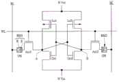
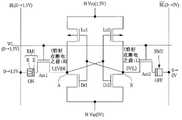
图1是示出根据本实施例的半导体存储器件(也称为半导体器件、半导体集成电路器件)的存储单元构造的等效电路图。FIG. 1 is an equivalent circuit diagram showing a memory cell configuration of a semiconductor memory device (also referred to as a semiconductor device, a semiconductor integrated circuit device) according to the present embodiment.
如图所示,根据本实施例的半导体存储器件是将数据存储在触发器单元(也称为FF单元或锁存单元)中的SRAM。触发器单元包括由四个晶体管构成的两个交叉耦合的CMOS反相器。将数据(“1”和“0”)存储在CMOS反相器的输入/输出部分中。“CMOS”是“互补金属氧化物半导体”的缩写。As shown in the figure, the semiconductor memory device according to the present embodiment is an SRAM that stores data in a flip-flop unit (also referred to as an FF unit or a latch unit). The flip-flop cell consists of two cross-coupled CMOS inverters consisting of four transistors. Store the data ("1" and "0") in the input/output section of the CMOS inverter. "CMOS" is an acronym for "Complementary Metal Oxide Semiconductor".
在本实施例中,ReRAM单元(非易失性单元)RM1和RM2经由存取晶体管设置在CMOS反相器的输入/输出部分中。“ReRAM”是“电阻随机存取存储器”的缩写,并且表示利用电阻随施加电压而变化的存储器。它也被称为“电阻变化存储器”。以此方式,根据本实施例的半导体存储器件具有SRAM的构造和ReRAM单元(非易失性存储单元)。因此,本半导体存储器件还可以被称为“非易失性SRAM”或“具有内置非易失性存储单元的SRAM”。In the present embodiment, ReRAM cells (nonvolatile cells) RM1 and RM2 are provided in the input/output section of the CMOS inverter via access transistors. "ReRAM" is an abbreviation for "resistive random access memory", and means a memory that utilizes a change in resistance with applied voltage. It is also called "resistance change memory". In this way, the semiconductor memory device according to the present embodiment has a configuration of an SRAM and a ReRAM cell (nonvolatile memory cell). Therefore, the present semiconductor memory device may also be called "nonvolatile SRAM" or "SRAM with built-in nonvolatile memory cells".
下面将参照图1详细说明存储单元构造。The memory cell configuration will be described in detail below with reference to FIG. 1 .
如图所示,存储单元布置在一对位线(位线BL和位线/BL(在后面的附图中具有上横线的“BL”))和字线WL的交叉点处。这个存储单元包括一对负载晶体管(也称为负载MOS、作为负载的晶体管、作为负载的MISFET)Lo1和Lo2、一对存取晶体管(也称为存取MOS、用于存取的晶体管、存取MISFET、用于传递的晶体管)Acc1和Acc2以及一对驱动晶体管(也称为驱动MOS、用于驱动的晶体管、用于驱动的MISFET)Dr1和Dr2。As shown in the figure, memory cells are arranged at intersections of a pair of bit lines (a bit line BL and a bit line /BL (“BL” with an upper horizontal line in later figures)) and a word line WL. This memory cell includes a pair of load transistors (also known as load MOS, transistor as load, MISFET as load) Lo1 and Lo2, a pair of access transistors (also known as access MOS, transistor for access, memory Take MISFET, transistor for passing) Acc1 and Acc2 and a pair of driving transistors (also known as driving MOS, transistor for driving, MISFET for driving) Dr1 and Dr2.
在构成存储单元的六个晶体管之中,负载晶体管(Lo1、Lo2)是p型(p沟道型)晶体管,并且存取晶体管(Acc1、Acc2)和驱动晶体管(Dr1、Dr2)是n型(n沟道型)晶体管。Among the six transistors constituting the memory cell, the load transistors (Lo1, Lo2) are p-type (p-channel type) transistors, and the access transistors (Acc1, Acc2) and drive transistors (Dr1, Dr2) are n-type ( n-channel type) transistor.
“MISFET”是“金属绝缘半导体场效应晶体管”的缩写并且可以被称为MOS。下文中,负载晶体管、存取晶体管和驱动晶体管可以被简称为“晶体管”。可以只通过每个晶体管的符号(Lo1、Lo2、Acc1、Acc2、Dr1、Dr2)表示每个晶体管。"MISFET" is an abbreviation for "Metal Insulator Semiconductor Field Effect Transistor" and may be referred to as MOS. Hereinafter, load transistors, access transistors, and drive transistors may be simply referred to as "transistors." Each transistor can be represented only by its symbol (Lo1, Lo2, Acc1, Acc2, Dr1, Dr2).
在构成存储单元的六个晶体管之中,Lo1和Acc1构成一个CMOS反相器,并且Lo2和Acc2构成另一个CMOS反相器。这些成对的CMOS反相器的输入/输出部分(存储节点A、B)相互交叉耦合,并且构成触发器单元(FF单元),作为存储1位信息的信息存储单元。Among the six transistors constituting the memory cell, Lo1 and Acc1 constitute one CMOS inverter, and Lo2 and Acc2 constitute another CMOS inverter. The input/output parts (storage nodes A, B) of these pairs of CMOS inverters are cross-coupled to each other, and constitute a flip-flop unit (FF unit) as an information storage unit that stores 1-bit information.
下面说明构成SRAM存储单元的六个晶体管的耦合关系的全部细节。Full details of the coupling relationship of the six transistors constituting the SRAM memory cell are described below.
Lo1耦合在电源电势节点(电源节点)NVcc和存储节点(第一节点)A之间,Dr1耦合在存储节点A和基准电势节点(低电势节点)NVss之间,并且Lo1和Dr1的栅电极耦合到存储节点(第二节点)B。在随后将描述的SRAM的正常操作时间段内向电源电势节点NVcc施加第一电源电势Vcc,并且在随后将描述的待机时间段之前和之后向电源电势节点NVcc施加第二电源电势Vcc2和第三电源电势Vcc3。向基准电势节点NVss施加比第一、第二和第三电源电势(Vcc1、Vcc2、Vcc3)低的电势,在当前情况下,即基准电势(也称为0V、地电势、地)。例如,第一电源电势Vcc是1.5V。第二电源电势Vcc2是比第一电源电势Vcc高的电势,例如,是2.0V。第三电源电势Vcc3是比第二电源电势Vcc2高的电势,例如,是3.5V。Lo1 is coupled between the power supply potential node (power supply node) NVcc and the storage node (first node) A, Dr1 is coupled between the storage node A and the reference potential node (low potential node) NVss, and the gate electrodes of Lo1 and Dr1 are coupled to storage node (second node) B. The first power supply potential Vcc is applied to the power supply potential node NVcc during a normal operation period of the SRAM to be described later, and the second power supply potential Vcc2 and the third power supply are applied to the power supply potential node NVcc before and after a standby period to be described later. Potential Vcc3. A potential lower than the first, second and third power supply potentials ( Vcc1 , Vcc2 , Vcc3 ), in the present case, a reference potential (also called 0V, ground potential, ground) is applied to the reference potential node NVss. For example, the first power supply potential Vcc is 1.5V. The second power supply potential Vcc2 is a higher potential than the first power supply potential Vcc, for example, 2.0V. The third power supply potential Vcc3 is a higher potential than the second power supply potential Vcc2, for example, 3.5V.
Lo2耦合在电源电势节点NVcc和存储节点B之间,Dr2耦合在存储节点B和基准电势节点NVss之间,并且Lo2和Dr2的栅电极耦合到存储节点A。Lo2 is coupled between the power supply potential node NVcc and the storage node B, Dr2 is coupled between the storage node B and the reference potential node NVss, and the gate electrodes of Lo2 and Dr2 are coupled to the storage node A.
Acc1耦合到存储节点A,Acc2耦合到存储节点B,并且Acc1和Acc2的栅电极耦合到字线WL(它们用作字线)。例如,字线WL的驱动电势是第一电源电势Vcc(例如,1.5V)。Acc1 is coupled to storage node A, Acc2 is coupled to storage node B, and the gate electrodes of Acc1 and Acc2 are coupled to word line WL (they serve as word lines). For example, the driving potential of the word line WL is the first power supply potential Vcc (for example, 1.5V).
这里,根据本实施例,ReRAM单元RM1和RM2设置在SRAM存储单元中。ReRAM单元(RM1、RM2)具有电阻变化层(也称为存储器层、存储单元、状态变化层、电阻变化层、可变电阻层、相变层、磁性变化层)R。电阻变化层R具有第一端和第二端,并且电极部分E设置在第一端。ReRAM单元RM1的第一端(在电极部分E侧上)耦合到Acc1(在存储节点A的相对侧上的端部),并且第二端耦合到位线BL。ReRAM单元RM2的第一端(在电极部分E侧上)耦合到Acc2(在存储节点B的相对侧上的端部),并且第二端耦合到位线/BL。Here, according to the present embodiment, the ReRAM units RM1 and RM2 are provided in the SRAM memory unit. The ReRAM cell ( RM1 , RM2 ) has a resistance change layer (also referred to as memory layer, memory cell, state change layer, resistance change layer, variable resistance layer, phase change layer, magnetic change layer) R. The resistance change layer R has a first end and a second end, and the electrode part E is disposed at the first end. A first end (on the electrode portion E side) of the ReRAM cell RM1 is coupled to Acc1 (an end on the opposite side to the storage node A), and a second end is coupled to the bit line BL. A first end (on the electrode portion E side) of the ReRAM cell RM2 is coupled to Acc2 (an end on the opposite side of the storage node B), and a second end is coupled to the bit line /BL.
《电路操作》"Circuit Operation"
接着,说明ReRAM单元和SRAM的操作。Next, the operations of the ReRAM cell and the SRAM will be described.
<ReRAM单元的操作>图2是示出ReRAM单元的操作的电路图。当在第一端和第二端之间产生比预定电势(也称为特定电势、第一电势)高的电势差时,电阻变化层R改变其电阻。<Operation of ReRAM Cell> FIG. 2 is a circuit diagram showing the operation of the ReRAM cell. When a potential difference higher than a predetermined potential (also referred to as a specific potential, first potential) is generated between the first end and the second end, the resistance change layer R changes its resistance.
具体地,如图2A中所示,当向电阻变化层R的第二端施加第二电源电势Vcc2(2.0V)并且向电阻变化层R的第一端(在电极部分E侧上)施加比第二电源电势Vcc2低预定电势(这里,基准电势0V)的电势时,电阻变化层R变成低电阻状态。例如,预定电势是2.0V。如图2A中所示,在第一端和第二端之间产生比预定电势大的电势差并且施加到第二端的电势更高的情况被称为“正向偏置”。以此方式,当向电阻变化层R应用正向偏置时,电阻变化层R变成低电阻状态并且转为导通状态(ON)。也就是说,电流流过电阻变化层R。Specifically, as shown in FIG. 2A , when the second power supply potential Vcc2 (2.0 V) is applied to the second end of the resistance change layer R and the ratio When the second power supply potential Vcc2 is lower than the potential of a predetermined potential (here, the reference potential 0V), the resistance change layer R becomes a low resistance state. For example, the predetermined potential is 2.0V. As shown in FIG. 2A , the case where a potential difference greater than a predetermined potential is generated between the first terminal and the second terminal and the potential applied to the second terminal is higher is called "forward bias". In this way, when a forward bias is applied to the resistance change layer R, the resistance change layer R becomes a low resistance state and turns into a conduction state (ON). That is, current flows through the resistance change layer R.
另一方面,如图2B中所示,当向电阻变化层R的第一端(在电极部分E侧上)施加第二电源电势Vcc2(2.0V),向电阻变化层R的第二端施加比第二电源电势Vcc2低预定电势(这里,基准电势0V)的电势时,电阻变化层R变成高电阻状态。例如,预定电势是2.0V。如图2B中所示,在第一端和第二端之间产生比预定电势大的电势差并且施加到第一端的电势更高的情况被称为“反向偏置”。以此方式,当向电阻变化层R应用反向偏置时,电阻变化层R变成高电阻状态并且转为截止状态(OFF)。也就是说,电流几乎没有流过电阻变化层R。On the other hand, as shown in FIG. 2B , when the second power supply potential Vcc2 (2.0 V) is applied to the first end of the resistance change layer R (on the electrode portion E side), the second end of the resistance change layer R is applied At a potential lower than the second power supply potential Vcc2 by a predetermined potential (here, the reference potential 0V), the resistance change layer R becomes a high resistance state. For example, the predetermined potential is 2.0V. As shown in FIG. 2B , the case where a potential difference greater than a predetermined potential is generated between the first terminal and the second terminal and the potential applied to the first terminal is higher is called "reverse bias". In this way, when a reverse bias is applied to the resistance change layer R, the resistance change layer R becomes a high resistance state and turns to an off state (OFF). That is, the current hardly flows through the resistance change layer R.
当电阻变化层R的第一端和第二端之间的电势差小于预定电势时,没有产生电阻变化并且维持直到该时刻(导通状态或截止状态)之前的状态。When the potential difference between the first end and the second end of the resistance change layer R is smaller than a predetermined potential, no resistance change occurs and the state up to that point (on state or off state) is maintained.
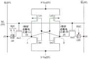
<SRAM的操作>(SRAM的正常操作)接着,说明SRAM的正常操作。图3是示出SRAM操作的电路图。<Operation of SRAM> (Normal Operation of SRAM) Next, the normal operation of the SRAM will be described. FIG. 3 is a circuit diagram showing the operation of the SRAM.
在SRAM的正常操作时间段(第一时间段)内,ReRAM单元RM1和RM2两者都保持在导通状态(ON),使得ReRAM单元RM1和RM2不会妨碍SRAM的操作。During the normal operation period (first period) of the SRAM, both the ReRAM cells RM1 and RM2 are kept in the conduction state (ON), so that the ReRAM cells RM1 and RM2 do not hinder the operation of the SRAM.
也就是说,当CMOS反相器的存储节点B是高电势(H电平、第二电平、H=1.5V)时,Dr1处于导通状态;因此,另一个CMOS反相器的存储节点A变成低电势(L电平、第一电平、L=0V)。因此,Lo2变成导通状态并且保持存储节点B的高电势(H=1.5V)。也就是说,通过由一对交叉耦合的CMOS反相器构成的触发器单元将存储节点A和B的状态相互保持,并且存储(保留)数据(信息)。That is to say, when the storage node B of the CMOS inverter is at a high potential (H level, second level, H=1.5V), Dr1 is in the conduction state; therefore, the storage node of another CMOS inverter A becomes a low potential (L level, first level, L=0V). Therefore, Lo2 becomes on-state and maintains the high potential of the storage node B (H=1.5V). That is, the states of the storage nodes A and B are held mutually by a flip-flop cell composed of a pair of cross-coupled CMOS inverters, and data (information) is stored (retained).
另一方面,字线WL耦合到Acc1和Acc2的栅电极中的每一个。也就是说,当字线WL处于高电势(H=1.5V)时,Acc1和Acc2处于导通状态并且触发器电路和位线(BL和/BL)电耦合。因此,存储节点A和B的电势状态(H和L的组合或L和H的组合)出现在位线BL和/BL中并且被读取作为存储单元的数据。On the other hand, the word line WL is coupled to each of the gate electrodes of Acc1 and Acc2. That is, when the word line WL is at a high potential (H=1.5V), Acc1 and Acc2 are in a conduction state and the flip-flop circuit and the bit lines (BL and /BL) are electrically coupled. Therefore, the potential states of the storage nodes A and B (a combination of H and L or a combination of L and H) appear in the bit lines BL and /BL and are read as data of the memory cell.
当将信息写入存储单元时,字线WL被设置成高电势(H=1.5V),并且Acc1和Acc2被控制成导通状态;因此,触发器电路和位线(BL和/BL)电耦合,并且位线BL和/B的信息(H和L的组合或L和H的组合)被传递(写入)到存储节点A和B,从而如上所述地存储数据。When writing information into a memory cell, the word line WL is set to a high potential (H=1.5V), and Acc1 and Acc2 are controlled to be in a conductive state; therefore, the flip-flop circuit and the bit line (BL and /BL) electric potential are coupled, and the information (combination of H and L or combination of L and H) of the bit lines BL and /B is transferred (written) to the storage nodes A and B, thereby storing data as described above.
(待机操作)接着,说明从SRAM的正常操作时间段之后的待机时间段(第二时间段)直至SRAM的另一个正常操作时间段(第三时间段)的流程。(Standby Operation) Next, the flow from the standby period (second period) after the normal operation period of the SRAM to another normal operation period of the SRAM (third period) will be described.
图4是示出根据本实施例的半导体存储器件的操作的流程图。在上述的SRAM的正常操作时间段ST1中,执行SRAM的正常操作、数据存储、读取、写入等。在这种情况下,如上所述,ReRAM单元RM1和RM2两者都处于导通状态,并且ReRAM单元RM1和RM2没有妨碍SRAM的操作。FIG. 4 is a flowchart showing the operation of the semiconductor memory device according to the present embodiment. In the above-described normal operation period ST1 of the SRAM, normal operation of the SRAM, data storage, reading, writing, and the like are performed. In this case, as described above, both the ReRAM cells RM1 and RM2 are in the ON state, and the ReRAM cells RM1 and RM2 do not hinder the operation of the SRAM.
此后,响应于CPU(中央处理单元)的指令,例如,响应于待机信号的上升,SRAM进入待机状态(ST2)。响应于待机信号的上升,设置ReRAM单元RM1和RM2(ST3)。具体地,在SRAM的正常操作时间段ST1的结束时间,例如,在待机信号的上升时间,将SRAM保留的数据(存储节点A和B的电势状态、存储节点A和B的H和L的组合)写入ReRAM单元RM1和RM2。换言之,关于两个ReRAM单元RM1和RM2的状态(导通状态和截止状态的组合)存储存储节点A和B的电势状态。Thereafter, in response to an instruction of the CPU (Central Processing Unit), for example, in response to rising of a standby signal, the SRAM enters a standby state ( ST2 ). In response to rising of the standby signal, ReRAM cells RM1 and RM2 are set (ST3). Specifically, at the end time of the normal operation period ST1 of the SRAM, for example, at the rising time of the standby signal, the data retained by the SRAM (the potential states of the storage nodes A and B, the combination of H and L of the storage nodes A and B ) into ReRAM cells RM1 and RM2. In other words, the potential states of the storage nodes A and B are stored with respect to the states (combination of on-state and off-state) of the two ReRAM cells RM1 and RM2 .
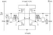
图5是示出将SRAM的保留的数据写入ReRAM单元的操作实例的电路图。在SRAM的正常操作时间段ST1的结束时间,例如,当在存储节点A处保持低电势(L=0V)并且在存储节点B处保持高电势(H=1.5V)时,如参照图3说明的,ReRAM单元RM1被设置成导通状态(ON)并且ReRAM单元RM2被设置成截止状态(OFF)。FIG. 5 is a circuit diagram showing an operation example of writing retained data of an SRAM into a ReRAM cell. At the end time of the normal operation period ST1 of the SRAM, for example, when a low potential (L=0V) is maintained at the storage node A and a high potential (H=1.5V) is maintained at the storage node B, as explained with reference to FIG. 3 Yes, the ReRAM cell RM1 is set to a conduction state (ON) and the ReRAM cell RM2 is set to an off state (OFF).
如上所述,ReRAM单元RM1和RM2两者都已处于导通状态(ON),因此,ReRAM单元RM1维持导通状态(ON)并且ReRAM单元RM2从导通状态(ON)转变为截止状态(OFF)。As described above, both the ReRAM cells RM1 and RM2 are already in the conduction state (ON), therefore, the ReRAM cell RM1 maintains the conduction state (ON) and the ReRAM cell RM2 transitions from the conduction state (ON) to the cut-off state (OFF ).
具体地,如图5中所示,为了将ReRAM单元RM2从导通状态变为截止状态,<1>施加到电源电势节点NVcc的电势从第一电源电势Vcc(1.5V)改变为第二电源电势Vcc2(2.0V)。因此,<2>存储节点B的电势从1.5V上升为2.0V。在这种情况下,因为字线WL处于第一电源电势Vcc(1.5V),所以第二电源电势Vcc2(2.0V)经由Acc2施加到电阻变化层R的第一端(在电极部分E侧上)。另一方面,因为位线/BL仍处于低电势(0V),所以将0V施加到电阻变化层R的第二端。因此,<3>在电阻变化层R的第一端和第二端之间产生大于预定电势(2.0V)的电势差,并且出现施加到第一端的电势高的所谓“反向偏置”的状态。因此,电阻变化层R转变成高电阻状态,并且ReRAM单元RM2从导通状态(ON)变成截止状态(OFF)(ReRAM单元RM2被重新写入)。Specifically, as shown in FIG. 5 , in order to change the ReRAM cell RM2 from the on state to the off state, <1> the potential applied to the power supply potential node NVcc is changed from the first power supply potential Vcc (1.5 V) to the second power supply Potential Vcc2 (2.0V). Therefore, <2> the potential of the storage node B rises from 1.5V to 2.0V. In this case, since the word line WL is at the first power supply potential Vcc (1.5V), the second power supply potential Vcc2 (2.0V) is applied to the first end (on the electrode portion E side) of the resistance change layer R via Acc2 ). On the other hand, since the bit line /BL is still at a low potential (0V), 0V is applied to the second terminal of the resistance change layer R. Therefore, <3> a potential difference greater than a predetermined potential (2.0 V) is generated between the first terminal and the second terminal of the resistance change layer R, and a so-called "reverse bias" in which the potential applied to the first terminal is high occurs state. Accordingly, the resistance change layer R transitions to a high resistance state, and the ReRAM cell RM2 changes from the on state (ON) to the off state (OFF) (the ReRAM cell RM2 is rewritten).
以此方式,通过比第一电源电势Vcc(1.5V)高的预定电势(2.0V)执行重新写入。换言之,通过采用仅利用比第一电源电势Vcc(1.5V)高的预定电势(2.0V)而表现电阻变化的ReRAM单元(电阻变化层R),能够防止在SRAM正常操作时发生重新写入,然而,在必要时,能够执行将SRAM保留的数据写入到ReRAM单元。In this way, rewriting is performed with a predetermined potential (2.0 V) higher than the first power supply potential Vcc (1.5 V). In other words, by employing a ReRAM cell (resistance change layer R) that exhibits resistance change only with a predetermined potential (2.0 V) higher than the first power supply potential Vcc (1.5 V), rewriting can be prevented from occurring at the time of normal operation of the SRAM, However, writing of data retained by the SRAM to the ReRAM cell can be performed when necessary.
在ReRAM单元RM1中,即使当第一电源电势Vcc(1.5V)施加到字线WL并且Acc1处于导通状态时,位线BL处于低电势(0V)并且存储节点A维持在低电势(L=0V)。因此,在电阻变化层R的第一端和第二端之间没有产生电势差。因此,ReRAM单元RM1没有被重新写入,而是维持导通状态(ON)。In the ReRAM cell RM1, even when the first power supply potential Vcc (1.5 V) is applied to the word line WL and Acc1 is in the on state, the bit line BL is at a low potential (0 V) and the storage node A is maintained at a low potential (L= 0V). Therefore, no potential difference is generated between the first end and the second end of the resistance change layer R. Referring to FIG. Therefore, the ReRAM cell RM1 is not rewritten, but maintains the conduction state (ON).
图6A和图6B是示出在写入到ReRAM单元时所施加的电压的横截面示意图。图6A对应于图5所示的ReRAM单元RM1,并且图6B对应于图5所示的ReRAM单元RM2。6A and 6B are schematic cross-sectional views showing voltages applied when writing to a ReRAM cell. FIG. 6A corresponds to the ReRAM unit RM1 shown in FIG. 5 , and FIG. 6B corresponds to the ReRAM unit RM2 shown in FIG. 5 .
因为如图6A中所示的字线WL(栅电极)是1.5V,所以存储节点A的电势(0V)经由处于导通状态的Acc1施加到ReRAM单元RM1的电阻变化层R的第一端(在电极部分E侧上)。因为位线BL的电势是0V,所以0V施加到电阻变化层R的第二端。以此方式,在第一端和第二端之间没有产生电势差;因此,没有发生重新写入并且ReRAM单元RM1维持导通状态(ON)。Since the word line WL (gate electrode) as shown in FIG. 6A is 1.5 V, the potential (0 V) of the storage node A is applied to the first end of the resistance change layer R of the ReRAM cell RM1 via Acc1 in the on state ( on the electrode part E side). Since the potential of the bit line BL is 0V, 0V is applied to the second terminal of the resistance change layer R. In this way, no potential difference is generated between the first terminal and the second terminal; therefore, rewriting does not occur and the ReRAM cell RM1 maintains the conduction state (ON).
因为如图6B中所示的字线WL(栅电极)是1.5V,所以存储节点B的电势(2.0V)经由处于导通状态的Acc2施加到ReRAM单元RM2的电阻变化层R的第一端(在电极部分E侧上)。因为位线/BL的电势是0V,所以0V施加到电阻变化层R的第二端。以此方式,在将0V施加到第二端,2.0V施加到第一端并且施加到第一端的电势高的状态下,产生电阻变化所需的电势差。因此,电阻变化层R变成高电阻状态。因此,ReRAM单元RM2被重新写入并且从导通状态(ON)转变成截止状态(OFF)。Since the word line WL (gate electrode) as shown in FIG. 6B is 1.5 V, the potential (2.0 V) of the storage node B is applied to the first end of the resistance change layer R of the ReRAM cell RM2 via Acc2 in the on state (on the electrode part E side). Since the potential of the bit line /BL is 0V, 0V is applied to the second terminal of the resistance change layer R. In this way, in a state where 0 V is applied to the second terminal, 2.0 V is applied to the first terminal, and the potential applied to the first terminal is high, a potential difference required for resistance change is generated. Therefore, the resistance change layer R becomes a high resistance state. Accordingly, the ReRAM cell RM2 is rewritten and transitions from the on state (ON) to the off state (OFF).
在完成对ReRAM单元RM1和RM2的写入操作(设置)之后,施加到电源电势节点NVcc的电势被设置成低电势(0V),从而进入断电状态(待机时间段)(ST4,图4)。图7是示出断电状态下每个部分的电势的电路图。如图7中所示,施加到电源电势节点NVcc的电势从2.0V变成0V。在这种情况下,字线WL的电势也被无效。也就是说,字线WL的电势从1.5V变成0V,并且Acc1和Acc2转变为截止状态。通过使电源电势节点NVcc无效,存储节点A和B的保留电势(数据)消失,并且存储节点A和B的电势变成例如0V。然而,对应的数据被存储(保留)作为两个ReRAM单元RM1和RM2的状态(导通状态和截止状态的组合)。在本情况下,ReRAM单元RM1被设置成导通状态(ON)并且ReRAM单元RM2被设置成截止状态(OFF);从而存储(保留)存储节点A和B恰好在断电(A=L且B=H)之前的电势。After completion of the write operation (setting) to the ReRAM cells RM1 and RM2, the potential applied to the power supply potential node NVcc is set to a low potential (0V), thereby entering a power-off state (standby period) (ST4, FIG. 4 ) . Fig. 7 is a circuit diagram showing the potential of each part in a power-off state. As shown in FIG. 7, the potential applied to the power supply potential node NVcc is changed from 2.0V to 0V. In this case, the potential of the word line WL is also invalidated. That is, the potential of the word line WL is changed from 1.5V to 0V, and Acc1 and Acc2 are turned into an off state. By invalidating the power supply potential node NVcc, the reserved potentials (data) of the storage nodes A and B disappear, and the potentials of the storage nodes A and B become, for example, 0V. However, the corresponding data is stored (retained) as the states (combination of on-state and off-state) of the two ReRAM cells RM1 and RM2 . In the present case, the ReRAM cell RM1 is set to the conduction state (ON) and the ReRAM cell RM2 is set to the cut-off state (OFF); thus storing (reserving) the storage nodes A and B exactly at power-off (A=L and B =H) before the potential.
接着,下面说明SRAM再次从待机时间段转变成正常操作的情况。例如,通过来自CPU的指令,响应于待机信号的下降,取消待机状态(ST5,图4)。在这种情况下,响应于待机信号的下降,施加到电源电势节点NVcc的电势从0V变成1.5V。也就是说,状态变成通电状态(ST6,图4)。图8是示出从断电状态变为通电状态时的电势变化的电路图。如图8中所示,施加到电源电势节点NVcc的电势从0V上升为1.5V。在这种情况下,除了电源电势节点NVcc之外的每个区域的电势状态与图7所示的情况相同,并且存储节点A和B的电势仍为0V。Next, the following describes the case where the SRAM transitions from the standby period to the normal operation again. For example, the standby state is canceled in response to the fall of the standby signal by an instruction from the CPU ( ST5 , FIG. 4 ). In this case, the potential applied to the power supply potential node NVcc is changed from 0V to 1.5V in response to the fall of the standby signal. That is, the state changes to the power-on state (ST6, FIG. 4). FIG. 8 is a circuit diagram showing a change in potential when changing from a power-off state to a power-on state. As shown in FIG. 8, the potential applied to the power supply potential node NVcc rises from 0V to 1.5V. In this case, the potential state of each region other than the power supply potential node NVcc is the same as the case shown in FIG. 7, and the potentials of the storage nodes A and B are still 0V.
接着,响应于待机信号的下降,读取ReRAM单元RM1和RM2的数据(ST7,图4),并且对应的数据被写入回存储节点A和B。然后,ReRAM单元RM1和RM2都被设置成导通状态(重新设置)(ST8,图4)。Next, in response to the fall of the standby signal, the data of the ReRAM cells RM1 and RM2 are read ( ST7 , FIG. 4 ), and the corresponding data is written back to the storage nodes A and B. Then, both the ReRAM cells RM1 and RM2 are set to the on state (reset) (ST8, FIG. 4).
图9是示出ReRAM单元中的数据读取操作(数据确定操作)的第一状态的电路图。如图9中所示,将字线WL从0V设置成驱动电势(1.5V),并且将位线BL和/BL两者都从0V设置成高电势(1.5V=H)。在这种情况下,因为ReRAM单元RM1处于导通状态(ON),所以存储节点A被设置成H(1.5V)并且Dr2被设置成导通状态。因此,存储节点B被设置成L(0V)。以此方式,通过将位线BL和/BL两者都设置成高电势(1.5V=H),H被写入(存储)到在处于导通状态(ON)的ReRAM单元(这里,RM1)侧上的存储节点(这里,A),并且在处于截止状态(OFF)的ReRAM单元(这里,RM2)侧上的存储节点(这里,B)被设置成L。以此方式,仅通过将位线BL和/BL两者从0V激活为高电势(1.5V=H),可以以自匹配方式(自动地)执行ReRAM单元的数据传递。也就是说,响应于在ReRAM单元RM1和RM1中写入的数据(这里,导通和截止的组合),存储节点A和B的电势改变(这里,变成A=H且B=L)。电势的当前状态(A=H且B=L)与恰好在断电之前的存储节点A和B的电势状态(A=L且B=H)相反。FIG. 9 is a circuit diagram showing a first state of a data read operation (data determination operation) in the ReRAM cell. As shown in FIG. 9 , the word line WL is set from 0V to a driving potential (1.5V), and both the bit lines BL and /BL are set from 0V to a high potential (1.5V=H). In this case, since the ReRAM cell RM1 is in the conduction state (ON), the storage node A is set to H (1.5V) and Dr2 is set to the conduction state. Therefore, the storage node B is set to L (0V). In this way, by setting both the bit lines BL and /BL to high potential (1.5V=H), H is written (stored) to the ReRAM cell (here, RM1) in the conducting state (ON) The storage node (here, A) on the side, and the storage node (here, B) on the side of the ReRAM cell (here, RM2 ) in the off state (OFF) is set to L. In this way, data transfer of the ReRAM cell can be performed in a self-matching manner (automatically) only by activating both the bit lines BL and /BL from 0V to a high potential (1.5V=H). That is, in response to data written in the ReRAM cells RM1 and RM1 (here, a combination of on and off), the potentials of the storage nodes A and B change (here, become A=H and B=L). The current state of potential (A=H and B=L) is opposite to the potential state of storage nodes A and B (A=L and B=H) just before power-off.
接着,使字线WL和位线BL和/BL失效。图10是示出ReRAM单元中的数据读取操作(数据确定操作)的第二状态的电路图。如图10中所示,字线WL和位线BL和/BL失效,从1.5V到0V。以此方式,即使当字线WL和位线BL和/BL失效时,与ReRAM单元RM1和RM2中写入的数据对应的电势维持在存储节点A和B中。Next, the word line WL and the bit lines BL and /BL are disabled. FIG. 10 is a circuit diagram showing a second state of a data read operation (data determination operation) in the ReRAM cell. As shown in Figure 10, word line WL and bit lines BL and /BL fail from 1.5V to 0V. In this way, potentials corresponding to data written in ReRAM cells RM1 and RM2 are maintained in storage nodes A and B even when word line WL and bit lines BL and /BL fail.
接着,将字线WL从0V激活为1.5V,并且存储节点A和B的电势经由Acc1和Acc2被传递到位线BL和/BL。也就是说,读取ReRAM单元的数据。图11是示出ReRAM单元中的数据读取操作(数据确定操作)的第三状态的电路图。如图11中所示,响应于字线WL的激活,位线BL和/BL的电势改变。在本情况下,位线BL从0V变成1.5V(H)并且位线/BL维持0V。通过位线的电势变化,已证明,存储节点A已经为H并且在存储节点A侧上的ReRAM单元RM1已处于导通状态。以此方式,能够基于位线BL和/BL中出现的电势,确定(读取)ReRAM单元RM1和RM2中的哪一个已处于导通状态。换言之,当位线BL和/BL的电势是H和L的组合时,已证明,在位线BL侧上的ReRAM单元RM1已处于导通状态,也就是说,恰好在断电之前,存储节点A已处于L状态。相反地,当位线BL和/BL的电势是L和H的组合时,已证明,在位线/BL侧上的ReRAM单元RM2已处于导通状态,也就是说,恰好在断电之前,存储节点B已处于L状态。以此方式,通过读取ReRAM单元RM1和RM2的数据,能够确定恰好在断电之前存储节点A和B的电势状态(ST7)。Next, the word line WL is activated from 0 V to 1.5 V, and the potentials of the storage nodes A and B are transferred to the bit lines BL and /BL via Acc1 and Acc2. That is, the data of the ReRAM cell is read. FIG. 11 is a circuit diagram showing a third state of a data read operation (data determination operation) in the ReRAM cell. As shown in FIG. 11, in response to activation of the word line WL, the potentials of the bit lines BL and /BL change. In this case, the bit line BL changes from 0V to 1.5V (H) and the bit line /BL maintains 0V. By the potential change of the bit line, it is proved that the storage node A has been H and the ReRAM cell RM1 on the storage node A side has been in the ON state. In this way, it is possible to determine (read) which of the ReRAM cells RM1 and RM2 has been in the on state based on the potentials appearing in the bit lines BL and /BL. In other words, when the potentials of the bit lines BL and /BL are a combination of H and L, it has been proved that the ReRAM cell RM1 on the side of the bit line BL is already in the on state, that is, just before the power-off, the storage node A is already in L state. Conversely, when the potentials of the bit lines BL and /BL are a combination of L and H, it turns out that the ReRAM cell RM2 on the side of the bit line /BL is already in the ON state, that is, just before power-off, Storage node B is already in the L state. In this way, by reading the data of the ReRAM cells RM1 and RM2 , it is possible to determine the potential states of the storage nodes A and B immediately before power-off ( ST7 ).
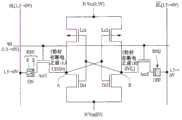
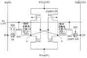
接着,将从ReRAM单元RM1和RM2读取的数据写入回存储节点A和B(ST8)。换言之,基于恰好在断电之前存储节点A和B的电势确定(这里,A=L且B=H)的数据被写入回存储节点A和B。图12是示出ReRAM单元的保留的数据到SRAM的写入操作(数据恢复操作)实例的电路图。Next, the data read from the ReRAM cells RM1 and RM2 are written back to the storage nodes A and B ( ST8 ). In other words, data determined based on the potentials of the storage nodes A and B just before power-off (here, A=L and B=H) is written back to the storage nodes A and B. FIG. 12 is a circuit diagram showing an example of a write operation (data recovery operation) of retained data of the ReRAM cell to the SRAM.
如图12中所示,基于恰好在断电之前存储节点A和B的电势确定(这里,A=L且B=H),0V被施加到位线BL并且第三电源电势(3.5V)被施加到位线/BL。具体地,在施加到电源电势节点NVcc的电势是1.5V的通电状态下,[1]在已处于截止状态(OFF)的ReRAM单元(这里,RM2)侧上的位线/BL,换言之,在恰好在断电之前已被保持为“H”的存储节点B侧上的位线/BL,上升为第三电源电势(3.5V)。第三电源电势Vcc3是比第一电源电势Vcc(这里,1.5V)高预定电势(这里,2.0V)的电势,并且是比第二电源电势Vcc2高的电势。另一方面,在已处于导通状态(ON)的ReRAM单元(这里,RM1)侧上的位线BL,换言之,在恰好在断电之前已被保持为“L”的存储节点A侧上的位线BL,被设置成低电势(0V)。此时,字线WL已上升为1.5V。[2]ReRAM单元(这里,RM1)处于导通状态(ON),因此,位线BL的电势(0V)被传递到存储节点A,并且存储节点A的电势从1.5V变成0V(L)。由此,[3]Lo2变成导通状态,因此,[4]存储节点B从0V变成1.5V(H)。以此方式,存储节点A被设置成L,存储节点B被设置成H,并且所保留的数据(也就是说,恰好在断电之前存储节点A和B的电势)被写入回存储节点A和B。As shown in FIG. 12 , based on the potential determination of the storage nodes A and B just before power-off (here, A=L and B=H), 0 V is applied to the bit line BL and the third power supply potential (3.5 V) is applied to the bit line /BL. Specifically, in the energized state where the potential applied to the power supply potential node NVcc is 1.5 V, [1] the bit line /BL on the side of the ReRAM cell (here, RM2 ) that has been in the off state (OFF), in other words, at The bit line /BL on the storage node B side, which has been held at "H" just before power-off, rises to the third power supply potential (3.5 V). The third power supply potential Vcc3 is a potential higher by a predetermined potential (here, 2.0 V) than the first power supply potential Vcc (here, 1.5 V), and is a higher potential than the second power supply potential Vcc2 . On the other hand, the bit line BL on the side of the ReRAM cell (here, RM1) that has been in the ON state (ON), in other words, the bit line BL on the side of the storage node A that has been held at "L" just before power-off The bit line BL is set to a low potential (0V). At this time, the word line WL has risen to 1.5V. [2] The ReRAM cell (here, RM1) is in the conduction state (ON), therefore, the potential (0V) of the bit line BL is transferred to the storage node A, and the potential of the storage node A is changed from 1.5V to 0V (L) . As a result, [3] Lo2 is turned on, and [4] the storage node B is changed from 0 V to 1.5 V (H). In this way, storage node A is set to L, storage node B is set to H, and the retained data (that is, the potentials of storage nodes A and B just before power-off) is written back to storage node A and B.
此外,存储节点B的电势(1.5V)被施加到电阻变化层R的第一端(在电极部分E侧上)。另一方面,位线/BL的电势(3.5V)被施加到电阻变化层R的第二端,并且在电阻变化层R中,在施加到第一端的电势较低的状态下产生电阻变化所需的电势差。因此,电阻变化层R变成低电阻状态。因此,[5]ReRAM单元RM2被重新写入并且其状态从截止状态(OFF)转变成导通状态(ON)。因此,数据被写入回SRAM,并且同时,ReRAM单元RM1和RM2两者都变成导通状态(ON),也就是说,两者都被重新设置。在这个时刻之后,SRAM的正常操作成为可能。也就是说,SRAM的正常操作、数据保持、读取、写入等成为可能,并且SRAM将返回到上述的正常操作时间段ST1。Further, the potential (1.5 V) of the storage node B is applied to the first end of the resistance change layer R (on the electrode portion E side). On the other hand, the potential (3.5 V) of the bit line /BL is applied to the second end of the resistance change layer R, and in the resistance change layer R, a resistance change occurs in a state where the potential applied to the first end is low required potential difference. Therefore, the resistance change layer R becomes a low resistance state. Accordingly, [5] the ReRAM cell RM2 is rewritten and its state is changed from the off state (OFF) to the on state (ON). Therefore, the data is written back to the SRAM, and at the same time, both the ReRAM cells RM1 and RM2 are turned ON, that is, both are reset. After this moment, normal operation of the SRAM becomes possible. That is, normal operation, data retention, reading, writing, etc. of the SRAM become possible, and the SRAM will return to the above-mentioned normal operation period ST1.
图13A和图13B是示出在重新设置ReRAM单元时所施加的电压的横截面示意图。图13A对应于图12所示的ReRAM单元RM1,并且图13B对应于图12所示的ReRAM单元RM2。13A and 13B are schematic cross-sectional views showing voltages applied when resetting a ReRAM cell. FIG. 13A corresponds to the ReRAM unit RM1 shown in FIG. 12 , and FIG. 13B corresponds to the ReRAM unit RM2 shown in FIG. 12 .
如图13A中所示,因为字线WL(栅电极)是1.5V,所以存储节点A的电势(0V)经由处于导通状态的Acc1施加到ReRAM单元RM1的电阻变化层R的第一端(在电极部分E侧上)。因为位线BL的电势是0V,所以0V被施加到电阻变化层R的第二端。以此方式,在第一端和第二端之间没有产生电势差;因此,没有发生重新写入并且ReRAM单元RM1维持导通状态(ON)。As shown in FIG. 13A , since the word line WL (gate electrode) is 1.5 V, the potential (0 V) of the storage node A is applied to the first end of the resistance change layer R of the ReRAM cell RM1 via Acc1 in the on state ( on the electrode part E side). Since the potential of the bit line BL is 0V, 0V is applied to the second end of the resistance change layer R. In this way, no potential difference is generated between the first terminal and the second terminal; therefore, rewriting does not occur and the ReRAM cell RM1 maintains the conduction state (ON).
如图13B中所示,因为字线WL(栅电极)是1.5V,所以存储节点B的电势(1.5V)经由处于导通状态的Acc2施加到ReRAM单元RM2的电阻变化层R的第一端(在电极部分E侧上)。因为位线BL的电势是3.5V,所以3.5V被施加到电阻变化层R的第二端。以此方式,在3.5V被施加到第二端,1.5V被施加到第一端并且施加到第一端的电势较低的状态下,产生电阻变化所需的电势差。因此,电阻变化层R变成低电阻状态。因此,ReRAM单元RM2被重新写入并且其状态从截止状态(OFF)转变成导通状态(ON)。As shown in FIG. 13B , since the word line WL (gate electrode) is 1.5 V, the potential (1.5 V) of the storage node B is applied to the first end of the resistance change layer R of the ReRAM cell RM2 via Acc2 in the on state (on the electrode part E side). Since the potential of the bit line BL is 3.5V, 3.5V is applied to the second terminal of the resistance change layer R. In this way, in a state where 3.5V is applied to the second terminal, 1.5V is applied to the first terminal, and the potential applied to the first terminal is lower, a potential difference required for resistance change is generated. Therefore, the resistance change layer R becomes a low resistance state. Accordingly, the ReRAM cell RM2 is rewritten and its state is changed from the off state (OFF) to the on state (ON).
以此方式,根据本实施例,通过在SRAM中设置ReRAM单元,能够继续存储在处于断电状态(待机状态)的SRAM的触发器单元中保持的数据。相反地,通过使ReRAM单元存储在SRAM的触发器单元中保持的数据,变得容易切断SRAM的电源,从而导致消耗电流的减小。也就是说,因为SRAM是易失性存储器,所以必须继续提供电力,以继续保持数据。然而,当不使用SRAM功能时,例如,当主要操作其它存储器时,能够使所关注的SRAM进入待机状态并且可以实现器件的低功耗。In this way, according to the present embodiment, by providing the ReRAM unit in the SRAM, it is possible to continue storing data held in the flip-flop unit of the SRAM in the power-off state (standby state). Conversely, by making the ReRAM cell store the data held in the flip-flop cell of the SRAM, it becomes easy to cut off the power supply of the SRAM, resulting in a reduction in consumption current. That is, since SRAM is a volatile memory, power must continue to be supplied to continue retaining data. However, when the SRAM function is not used, for example, when other memories are mainly operated, the SRAM concerned can be brought into a standby state and low power consumption of the device can be realized.
《器件结构》"Device Structure"
接着,参照截面图和平面图,说明根据本实施例的半导体存储器件的结构。Next, the structure of the semiconductor memory device according to the present embodiment will be described with reference to cross-sectional views and plan views.
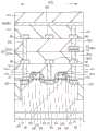
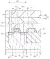
图14至图17是示出根据本实施例的半导体存储器件的存储单元构造的平面图。图18和图19是示出根据本实施例的半导体存储器件的存储单元构造的截面图。图18对应于图14的A-A横截面,并且图19对应于图14的B-B横截面。在平面图中,参照存储单元区MCA,通过重叠每个图,将使每个图中显示的图案的位置关系变得清楚。在本说明书中,为了使图简化,只示出随后将描述的有源区AcP1和AcN1的截面图。然而,与有源区AcP2和AcN2对应的横截面也具有类似结构。14 to 17 are plan views showing memory cell configurations of the semiconductor memory device according to the present embodiment. 18 and 19 are cross-sectional views showing the memory cell configuration of the semiconductor memory device according to the present embodiment. FIG. 18 corresponds to the A-A cross section of FIG. 14 , and FIG. 19 corresponds to the B-B cross section of FIG. 14 . In a plan view, referring to the memory cell area MCA, by overlapping each figure, the positional relationship of the patterns shown in each figure will be clarified. In this specification, in order to simplify the drawings, only sectional views of active regions AcP1 and AcN1 to be described later are shown. However, the cross sections corresponding to the active regions AcP2 and AcN2 also have similar structures.
如图18和图19中所示,在半导体衬底1上形成根据本实施例的半导体存储器件(具有内置ReRAM单元的SRAM)的存储单元。元件隔离区ST1布置在半导体衬底1上,并且被元件隔离区ST1划分的区域用作有源区(也称为元件形成区、半导体区)Ac。As shown in FIGS. 18 and 19 , memory cells of the semiconductor memory device (SRAM with built-in ReRAM cells) according to the present embodiment are formed on a
图14中示出的利用虚线围绕的大致矩形区域是一个(1位)存储单元区。如图中所示,四个有源区(AcP1、AcN1、AcN2、AcP2)沿着X方向顺序布置。这里,在指示有源区的符号“Ac”上加上标记,以识别各个区域。这些有源区(Ac)之间的区域是元件隔离区(STI)。换言之,如上所述,有源区(Ac)被元件隔离区(STI)分开。A substantially rectangular area surrounded by a dotted line shown in FIG. 14 is a one (1-bit) memory cell area. As shown in the figure, four active regions (AcP1, AcN1, AcN2, AcP2) are sequentially arranged along the X direction. Here, a mark is added to a symbol "Ac" indicating an active area to identify each area. The region between these active regions (Ac) is the element isolation region (STI). In other words, as described above, the active region (Ac) is separated by the element isolation region (STI).
阱(半导体区,nW、pW)布置在有源区(Ac)的半导体衬底1中(参照图18和图19)。换言之,有源区(Ac)对应于阱被暴露的区域。阱(nW、pW)的p型阱pW布置在两个有源区(AcP1、AcP2)各自的下部,并且n型阱nW布置在两个有源区(AcN1、AcN2)相应的下部。Wells (semiconductor regions, nW, pW) are arranged in the
如图14中所示,有源区AcP1具有在Y方向上延伸的线的形式。具体地,线的形式在随后描述的驱动晶体管Dr1的布置部分中具有的X方向宽度比存取晶体管Acc1的布置部分中的X方向宽度更宽。在图14中,线的形式在上部具有更宽的宽度。p型阱pW布置在有源区AcP 1的下部(参照图18)。As shown in FIG. 14, the active region AcP1 has the form of a line extending in the Y direction. Specifically, the form of the line has a wider X-direction width in an arrangement portion of the drive transistor Dr1 described later than in an arrangement portion of the access transistor Acc1 . In Fig. 14, the line form has a wider width in the upper part. The p-type well pW is arranged in the lower part of the active region AcP1 (refer to FIG. 18 ).
有源区AcN1具有矩形的形式,该矩形具有Y方向上的长边(图14)。n型阱nW布置在有源区AcN1的下部(参照图19)。The active region AcN1 has the form of a rectangle having a long side in the Y direction ( FIG. 14 ). An n-type well nW is arranged in the lower portion of the active region AcN1 (refer to FIG. 19 ).
有源区AcN2具有矩形的形式,该矩形具有Y方向上的长边(图14)。n型阱nW布置在有源区AcN2的下部(参照图19)。The active region AcN2 has the form of a rectangle having a long side in the Y direction ( FIG. 14 ). An n-type well nW is arranged in the lower portion of the active region AcN2 (refer to FIG. 19 ).
有源区AcP2具有在Y方向上延伸的线的形式。具体地,线的形式在随后描述的驱动晶体管Dr2的布置部分中具有的X方向宽度比在存取晶体管Acc2的布置部分中的X方向宽度更宽。在图14中,线的形式在下部具有更宽的宽度。p型阱pW布置在有源区AcP2的下部(参照图18)。The active region AcP2 has the form of a line extending in the Y direction. Specifically, the form of the line has a wider X-direction width in an arrangement portion of the drive transistor Dr2 described later than in an arrangement portion of the access transistor Acc2 . In Figure 14, the line form has a wider width in the lower part. A p-type well pW is arranged in a lower portion of the active region AcP2 (refer to FIG. 18 ).
如图14中所示,在四个有源区(AcP1、AcN1、AcN2、AcP2)上,经由栅极绝缘膜(GO,参照图18、图19等),栅电极(栅极布线)G(G1-G4)在X方向上延伸并跨越每个有源区,因此形成在上述“电路构造”中说明的六个晶体管。在栅电极G两侧上的有源区(Ac)用作晶体管的源-漏区(参照图18、图19等)。As shown in FIG. 14, on the four active regions (AcP1, AcN1, AcN2, AcP2), the gate electrode (gate wiring) G( G1-G4) extend in the X direction and span each active region, thus forming the six transistors explained in "Circuit Configuration" above. The active region (Ac) on both sides of the gate electrode G functions as a source-drain region of a transistor (refer to FIG. 18 , FIG. 19 , etc.).
具体地,公共栅电极G1被布置成跨越有源区AcP1和AcN1。因此,Dr1被布置在有源区AcP1上并且Lo1被布置在有源区AcN1上,并且这些栅电极(G)耦合在一起。这个公共栅电极G1延伸到有源区AcN2附近并且通过随后将描述的共用插塞SP1耦合到Lo2的源-漏区(参照图19)。Specifically, the common gate electrode G1 is arranged across the active regions AcP1 and AcN1. Therefore, Dr1 is arranged on the active region AcP1 and Lo1 is arranged on the active region AcN1 , and these gate electrodes (G) are coupled together. This common gate electrode G1 extends to the vicinity of the active region AcN2 and is coupled to the source-drain region of Lo2 through a common plug SP1 to be described later (refer to FIG. 19 ).
在有源区AcP1上,栅电极G2平行于上述的公共栅电极G1布置。因此,在有源区AcP1上,布置Acc1并且Dr1的源-漏区和Acc1的源-漏区耦合(公用)。On the active region AcP1, the gate electrode G2 is arranged parallel to the above-mentioned common gate electrode G1. Therefore, on the active region AcP1 , Acc1 is arranged and the source-drain region of Dr1 and the source-drain region of Acc1 are coupled (common).
公共栅电极G3被布置成跨越有源区AcP2和AcN2。因此,Dr2被布置在有源区AcP2上并且Lo2被布置在有源区AcN2上,并且这些栅电极(G)耦合在一起。这个公共栅电极G3延伸到有源区AcN1附近并且通过随后将描述的共用插塞SP1耦合到Lo2的源-漏区。The common gate electrode G3 is arranged across the active regions AcP2 and AcN2. Therefore, Dr2 is arranged on the active region AcP2 and Lo2 is arranged on the active region AcN2, and these gate electrodes (G) are coupled together. This common gate electrode G3 extends to the vicinity of the active region AcN1 and is coupled to the source-drain region of Lo2 through a common plug SP1 which will be described later.
在有源区AcP2上,栅电极G4平行于上述的公共栅电极G3布置。因此,在有源区AcP2上,布置Acc2并且Dr2的源-漏区和Acc2的源-漏区耦合(公用)。On the active region AcP2, the gate electrode G4 is arranged parallel to the above-mentioned common gate electrode G3. Therefore, on the active region AcP2, Acc2 is arranged and the source-drain region of Dr2 and the source-drain region of Acc2 are coupled (common).
四个栅电极G1-G4按2×2的方式布置在同一线上(对齐)。具体地,跨越有源区AcP1和AcN1的公共栅电极G1和有源区AcP2上的栅电极G4布置在沿着X方向延伸的同一线上。跨越有源区AcP2和AcN2的公共栅电极G3和有源区AcP1上的栅电极G2布置在沿着X方向延伸的同一线上。The four gate electrodes G1-G4 are arranged on the same line (aligned) in a 2×2 manner. Specifically, the common gate electrode G1 spanning the active regions AcP1 and AcN1 and the gate electrode G4 on the active region AcP2 are arranged on the same line extending along the X direction. The common gate electrode G3 spanning the active regions AcP2 and AcN2 and the gate electrode G2 on the active region AcP1 are arranged on the same line extending in the X direction.
在六个晶体管(Dr1、Acc1、Lo1、Lo2、Acc2、Dr2)的源-漏区域上,布置第一插塞P1(P1a-P1h)(图14)。第一插塞(耦合部)P1是与随后描述的第一层布线M1耦合的插塞。第一插塞P1还布置在四个栅电极(G1-G4)上。因为栅电极G1和G3上的第一插塞P1是构成“共用插塞”的第一插塞,所以它们被指示为如上所述的“SP1”。栅电极G2和G4上的第一插塞P1分别被指示为P1i和P1j。On the source-drain regions of the six transistors ( Dr1 , Acc1 , Lo1 , Lo2 , Acc2 , Dr2 ), first plugs P1 ( P1 a - P1 h ) are arranged ( FIG. 14 ). The first plug (coupling portion) P1 is a plug coupled with first layer wiring M1 described later. The first plug P1 is also arranged on the four gate electrodes ( G1 - G4 ). Since the first plugs P1 on the gate electrodes G1 and G3 are the first plugs constituting the "common plug", they are indicated as "SP1" as described above. The first plugs P1 on the gate electrodes G2 and G4 are indicated as P1i and P1j, respectively.
第一层布线M1布置在第一插塞P1(P1a-P1j,SP1)上(参照图15)。多布线层进一步布置在第一层布线M1上。例如,第二插塞P2和第二层布线M2布置在第一层布线M1上(参照图16),并且第三插塞P3、第三层布线M3等布置在第二层布线M2上(参照图17)。经由这些布线实现第一插塞P1之间的电耦合,并且实现图1所示晶体管之间的电耦合。The first layer wiring M1 is arranged on the first plugs P1 ( P1 a - P1 j , SP1 ) (refer to FIG. 15 ). Multiple wiring layers are further arranged on the first layer wiring M1. For example, the second plug P2 and the second layer wiring M2 are arranged on the first layer wiring M1 (refer to FIG. 16 ), and the third plug P3, the third layer wiring M3 and the like are arranged on the second layer wiring M2 (refer to Figure 17). The electrical coupling between the first plugs P1 is realized via these wirings, and the electrical coupling between the transistors shown in FIG. 1 is realized.
在本实施例中,如图15中所示,ReRAM单元RM1和RM2分别布置在第一插塞P1c和P1f上。第一插塞P1c对应于Acc1的一端(源-漏区)。Acc1的另一端耦合到如随后描述的与存储节点A相关的第一层布线M1A。也就是说,ReRAM单元RM1布置在位线BL和Acc1的另一端(源-漏区,具体是随后描述的第二插塞P2ca)之间,Acc1的一端(源-漏区)耦合到存储节点A。In this embodiment, as shown in FIG. 15 , ReRAM cells RM1 and RM2 are arranged on the first plugs P1c and P1f, respectively. The first plug P1c corresponds to one end (source-drain region) of Acc1. The other end of Acc1 is coupled to the first layer wiring M1A related to the storage node A as described later. That is, the ReRAM cell RM1 is arranged between the bit line BL and the other end (source-drain region, specifically the second plug P2ca described later) of Acc1, and one end (source-drain region) of Acc1 is coupled to the storage node a.
第一插塞P1f对应于Acc2的一端(源-漏区)。Acc2的另一端耦合到如随后描述的与存储节点B相关的第一层布线M1B。也就是说,ReRAM单元RM2布置在位线/BL和Acc2的另一端(源-漏区,具体是随后描述的第二插塞P2fa)之间,Acc2的一端(源-漏区)耦合到存储节点B。The first plug P1f corresponds to one end (source-drain region) of Acc2. The other end of Acc2 is coupled to the first layer wiring M1B related to the storage node B as described later. That is, the ReRAM cell RM2 is arranged between the bit line /BL and the other end (source-drain region, specifically the second plug P2fa described later) of Acc2, and one end (source-drain region) of Acc2 is coupled to the storage Node B.
只要实现了图1所示晶体管之间的耦合状态,第一插塞P1之间的具体耦合形式,例如,在第一层布线M1、第二插塞P2、第二层布线M2、第三插塞P3、第三层布线M3等的布局不受限制。下面说明布局的实例。As long as the coupling state between the transistors shown in FIG. The layout of the plug P3, the third-layer wiring M3, and the like is not limited. An example of the layout is described below.
如图15中所示,第一层布线M1被布置成将在Lo2和Dr2的公共栅电极G3上的共用插塞(共用接触)SP1耦合到在Dr1和Acc1的公共源-漏区上的第一插塞P1b。因为本第一层布线M1可以与图1的存储节点A相关,所以本第一层布线M1被标注为M1A。As shown in FIG. 15, the first layer wiring M1 is arranged to couple the common plug (common contact) SP1 on the common gate electrode G3 of Lo2 and Dr2 to the common plug (common contact) SP1 on the common source-drain region of Dr1 and Acc1. A plug P1b. Since the present first-layer wiring M1 may be related to the storage node A in FIG. 1 , the present first-layer wiring M1 is denoted as M1A.
第一层布线M1被布置成将Lo1和Dr1的公共栅电极G1上的共用插塞(共用接触)SP1耦合到Dr2和Acc2的公共源-漏区上的第一插塞P1b。因为本第一层布线M1可以与图1的存储节点B相关,所以本第一层布线M1被标注为M1B。The first layer wiring M1 is arranged to couple the common plug (common contact) SP1 on the common gate electrode G1 of Lo1 and Dr1 to the first plug P1b on the common source-drain region of Dr2 and Acc2. Since the present first-layer wiring M1 may be related to the storage node B in FIG. 1 , the present first-layer wiring M1 is denoted as M1B.
第一层布线(焊盘区)M1布置在第一插塞P1a、P1c、P1d、P1e、P1f、P1h、P1i和P1j中的每一个上。第二插塞P2(P2a、P2c、P2d、P2e、P2f、P2h和两个P2w)布置在每个第一层布线M1上(图15、图16)。A first layer wiring (land area) M1 is arranged on each of the first plugs P1a, P1c, P1d, P1e, P1f, P1h, P1i, and P1j. Second plugs P2 ( P2 a , P2 c , P2 d , P2 e , P2 f , P2 h and two P2 w ) are arranged on each first layer wiring M1 ( FIG. 15 , FIG. 16 ).
这里,由P2ca和P2cb形成第二插塞P2c,ReRAM单元RM1布置在P2ca和P2cb之间。具体地,第二插塞P2ca布置在位于第一插塞P1c上的第一层布线M1上,并且在第二插塞P2ca上布置形成ReRAM单元RM1的电极部分E和上部电阻变化层R,此外第二插塞P2cb布置在电阻变化层R上(参照图15、图16和图18)。由P2fa和P2fb形成第二插塞P2f,ReRAM单元RM2布置在P2fa和P2fb之间。具体地,第二插塞P2fa布置在位于第一插塞P1f上的第一层布线M1上,并且在第二插塞P2fa上,布置形成ReRAM单元RM2的电极部分E和上部电阻变化层R,此外第二插塞P2fb布置在电阻变化层R上(参照图15和图16)。Here, the second plug P2c is formed by P2ca and P2cb, and the ReRAM unit RM1 is disposed between P2ca and P2cb. Specifically, the second plug P2ca is arranged on the first layer wiring M1 located on the first plug P1c, and the electrode portion E forming the ReRAM cell RM1 and the upper resistance change layer R are arranged on the second plug P2ca, and furthermore The second plug P2cb is disposed on the resistance change layer R (refer to FIGS. 15 , 16 and 18 ). The second plug P2f is formed by P2fa and P2fb, and the ReRAM unit RM2 is disposed between P2fa and P2fb. Specifically, the second plug P2fa is arranged on the first layer wiring M1 located on the first plug P1f, and on the second plug P2fa, the electrode portion E and the upper resistance change layer R forming the ReRAM cell RM2 are arranged, Also the second plug P2fb is arranged on the resistance change layer R (refer to FIGS. 15 and 16 ).
如图16中所示,第二层布线M2布置在两个第二插塞P2i和P2j之间,并在X方向上延伸。该第二层布线M2用作字线WL。As shown in FIG. 16, the second layer wiring M2 is arranged between the two second plugs P2i and P2j, and extends in the X direction. This second layer wiring M2 functions as a word line WL.
第二层布线(焊盘区)M2布置在其它第二插塞P2(P2a、P2cb、P2d、P2e、P2fb、P2h)中的每一个上。A second layer wiring (land area) M2 is arranged on each of the other second plugs P2 ( P2 a , P2 cb , P2 d , P2 e , P2 fb , P2 h ).
如图17中所示,第三插塞P3(P3a、P3c、P3d、P3e、P3f、P3h)布置在相应的第二层布线M2上。As shown in FIG. 17 , third plugs P3 ( P3 a , P3 c , P3 d , P3 e , P3 f , P3 h ) are arranged on the corresponding second layer wiring M2 .
第三层布线M3布置在与第一插塞P1d和P1e耦合的第三插塞P3d和P3e之间,并在Y方向上延伸。该第三层布线M3用作电源电势线(VccL)。电源电势线(VccL)耦合到电源电势节点NVcc并且被供应有第一、第二和第三电源电势。The third layer wiring M3 is arranged between the third plugs P3d and P3e coupled with the first plugs P1d and P1e, and extends in the Y direction. This third layer wiring M3 serves as a power supply potential line (VccL). The power supply potential line (VccL) is coupled to the power supply potential node NVcc and is supplied with first, second and third power supply potentials.
第三层布线M3布置在与第一插塞P1a耦合的第三插塞P3a上,并在Y方向上延伸,并且第三层布线M3布置在与第一插塞P1h耦合的第三插塞P3h上,并在Y方向上延伸。这两个第三层布线M3分别用作基准电势线(VssL、地电势线)。The third layer wiring M3 is arranged on the third plug P3a coupled to the first plug P1a and extends in the Y direction, and the third layer wiring M3 is arranged on the third plug P3h coupled to the first plug P1h , and extend in the Y direction. These two third-layer wirings M3 serve as reference potential lines (VssL, ground potential lines), respectively.
第三层布线M3布置在与第一插塞P1c耦合的第三插塞P3c上,并在Y方向上延伸,并且第三层布线M3布置在与第一插塞P1f耦合的第三插塞P3f上,并在Y方向上延伸。这两个第三层布线M3用作位线(BL和/BL)。The third layer wiring M3 is arranged on the third plug P3c coupled with the first plug P1c, and extends in the Y direction, and the third layer wiring M3 is arranged on the third plug P3f coupled with the first plug P1f , and extend in the Y direction. These two third layer wirings M3 serve as bit lines (BL and /BL).
《制造过程》"Manufacturing process"
接着,参照图20至图27中示出的截面图,说明根据本实施例的半导体存储器件的制造过程,并且进一步阐明根据本实施例的半导体存储器件的构造。图20至图27是示出根据本实施例的半导体存储器件的制造过程的截面图。Next, referring to the sectional views shown in FIGS. 20 to 27 , the manufacturing process of the semiconductor memory device according to the present embodiment is explained, and the configuration of the semiconductor memory device according to the present embodiment is further clarified. 20 to 27 are cross-sectional views showing the manufacturing process of the semiconductor memory device according to the present embodiment.
如图20和图21中所示,元件隔离区STI形成在半导体衬底1中,该半导体衬底1例如是p型单晶硅衬底。有源区(Ac)被元件隔离区STI分开。As shown in FIGS. 20 and 21 , an element isolation region STI is formed in a
例如,可以通过采用STI(浅沟槽隔离)方法形成元件隔离区STI。也就是说,使用光刻技术和蚀刻技术,在半导体衬底1中形成元件隔离区STI。接着,通过采用CVD(化学气相沉积)方法等,在半导体衬底1上形成诸如氧化硅膜的绝缘膜,使其掩埋元件隔离凹槽。此后,通过化学-机械平面化(CMP)艺去除半导体衬底1上形成的不必要的氧化硅膜。因此,可以在氧化硅膜只嵌入在元件隔离凹槽中的情况下形成元件隔离区STI。For example, the element isolation region STI can be formed by employing an STI (Shallow Trench Isolation) method. That is, the element isolation region STI is formed in the
接着,在半导体衬底1中形成p型阱pW和n型阱nW。例如,通过采用离子注入方法,将p型杂质引入半导体衬底1,来形成p型阱pW。例如,通过采用离子注入方法,将n型杂质引入半导体衬底1,来形成n型阱nW。在引入杂质的过程中,不用说,通过形成合适的光致抗蚀剂膜(掩膜层)防止由于杂质注入导致在不必要的区域中引入杂质。Next, a p-type well pW and an n-type well nW are formed in the
接着,在作为在p型阱pW和n型阱nW的暴露区域的有源区(Ac)的主表面上,形成晶体管(Acc1、Dr1、Lo1、Acc2、Dr2、Lo2)中的每一个。Next, each of the transistors ( Acc1 , Dr1 , Lo1 , Acc2 , Dr2 , Lo2 ) is formed on the main surface of the active region (Ac) which is the exposed region in the p-type well pW and n-type well nW.
首先,在有源区(Ac)的主表面上,形成栅极绝缘膜GO。可以采用例如氧化硅膜作为栅极绝缘膜GO。例如,通过采用热氧化方法,在有源区(Ac)的表面上形成氧化硅膜。替代地,可以通过采用CVD方法形成氧化硅膜。优选都是采用氮氧化硅膜替代氧化硅膜。另外优选的是通过使用高介电常数膜(高k膜)形成栅极绝缘膜GO。另外优选的是通过使用由下层氧化硅膜和上层高介电常数膜(高k膜)组成的层叠膜来形成栅极绝缘膜GO。First, on the main surface of the active region (Ac), a gate insulating film GO is formed. A silicon oxide film, for example, can be used as the gate insulating film GO. For example, a silicon oxide film is formed on the surface of the active region (Ac) by employing a thermal oxidation method. Alternatively, a silicon oxide film may be formed by employing a CVD method. Preferably, a silicon nitride oxide film is used instead of the silicon oxide film. It is also preferable to form the gate insulating film GO by using a high dielectric constant film (high-k film). It is also preferable to form the gate insulating film GO by using a laminated film composed of a lower silicon oxide film and an upper high dielectric constant film (high-k film).
接着,在栅极绝缘膜GO上形成由导体膜组成的栅电极G。可以采用例如多晶硅膜作为栅电极G。例如,通过CVD方法等,在栅极绝缘膜GO上沉积多晶硅膜。接着,将光致抗蚀剂膜形成在多晶硅膜上、曝光和显影,然后,利用该光致抗蚀剂膜作为掩膜蚀刻多晶硅膜,并且形成栅电极G。从光致抗蚀剂膜的形成过程到蚀刻过程可以被称为图案化。优选的是采用金属膜作为栅电极G。另外优选的是通过采用由下层氧化硅膜和上层多晶硅膜组成的层叠膜形成栅电极G。以此方式,优选都是采用使用金属(包括具有金属导电性的化合物)作为栅电极的所谓金属栅极结构。Next, a gate electrode G composed of a conductive film is formed on the gate insulating film GO. As the gate electrode G, for example, a polysilicon film can be used. For example, by a CVD method or the like, a polysilicon film is deposited on the gate insulating film GO. Next, a photoresist film is formed on the polysilicon film, exposed to light, and developed, and then the polysilicon film is etched using the photoresist film as a mask, and a gate electrode G is formed. The process from the formation of the photoresist film to the etching process may be referred to as patterning. It is preferable to use a metal film as the gate electrode G. It is also preferable to form the gate electrode G by using a laminated film composed of a lower silicon oxide film and an upper polysilicon film. In this way, it is preferable to adopt a so-called metal gate structure using a metal (including a compound having metal conductivity) as a gate electrode.
接着,在栅电极G两侧上的有源区AcP1和AcP2和p型阱pW中形成n型低浓度杂质区EX。通过离子注入方法,通过利用栅电极G作为掩膜将n型杂质引入有源区(AcP1、AcP2、pW),来形成n型低浓度杂质区EX。接着,在栅电极G两侧的有源区AcN1和AcP2和n型阱nW中形成p型低浓度杂质区EX。通过离子注入方法,通过利用栅电极G作为掩膜将p型杂质引入有源区(AcN1、AcN2、nW),来形成p型低浓度杂质区EX。Next, an n-type low-concentration impurity region EX is formed in the active regions AcP1 and AcP2 on both sides of the gate electrode G and the p-type well pW. The n-type low-concentration impurity region EX is formed by introducing n-type impurities into the active regions (AcP1 , AcP2 , pW) by using the gate electrode G as a mask by an ion implantation method. Next, a p-type low-concentration impurity region EX is formed in the active regions AcN1 and AcP2 on both sides of the gate electrode G and the n-type well nW. The p-type low-concentration impurity region EX is formed by introducing p-type impurities into the active regions (AcN1 , AcN2 , nW) by using the gate electrode G as a mask by an ion implantation method.
接着,在栅电极G两侧的侧壁中形成侧壁膜SW。例如,通过CVD方法,在栅电极G上沉积通过由下层氧化硅膜和上侧氮化硅膜组成的层叠膜形成的绝缘膜,然后,通过各向异性蚀刻,在栅电极G的侧壁上形成由绝缘膜制成的侧壁膜SW。Next, sidewall films SW are formed in the sidewalls on both sides of the gate electrode G. As shown in FIG. For example, by the CVD method, an insulating film formed of a laminated film composed of a lower silicon oxide film and an upper silicon nitride film is deposited on the gate electrode G, and then, by anisotropic etching, on the side walls of the gate electrode G, A sidewall film SW made of an insulating film is formed.
接着,在栅电极G和侧壁膜SW的组合体的两侧的有源区(AcP1、AcP2、pW)中形成n型高浓度杂质区SD。例如,通过采用离子注入方法引入n型杂质,来形成n型高浓度杂质区SD。n型高浓度杂质区SD具有比n型低浓度杂质区EX的杂质浓度高的杂质浓度,并且其被形成为延伸到更深的位置。Next, n-type high-concentration impurity regions SD are formed in the active regions (AcP1 , AcP2 , pW) on both sides of the combination of the gate electrode G and the sidewall film SW. For example, the n-type high-concentration impurity region SD is formed by introducing n-type impurities by ion implantation. The n-type high-concentration impurity region SD has an impurity concentration higher than that of the n-type low-concentration impurity region EX, and is formed to extend to a deeper position.
接着,在栅电极G和侧壁膜SW的组合体的两侧的有源区(AcN1、AcN2、nW)中形成p型高浓度杂质区SD。例如,通过采用离子注入方法引入p型杂质,来形成p型高浓度杂质区SD。p型高浓度杂质区SD具有比p型低浓度杂质区EX的杂质浓度高的杂质浓度,并且其被形成为延伸到更深的位置。由高浓度杂质区SD和低浓度杂质区EX形成所谓LDD(轻掺杂漏极)结构的源-漏区。Next, p-type high-concentration impurity regions SD are formed in the active regions (AcN1 , AcN2 , nW) on both sides of the combination of the gate electrode G and the sidewall film SW. For example, the p-type high-concentration impurity region SD is formed by introducing p-type impurities using an ion implantation method. The p-type high-concentration impurity region SD has an impurity concentration higher than that of the p-type low-concentration impurity region EX, and is formed to extend to a deeper position. A source-drain region of a so-called LDD (Lightly Doped Drain) structure is formed by the high-concentration impurity region SD and the low-concentration impurity region EX.
根据以上过程,大致完成形成SRAM存储单元的六个晶体管(Dr1、Acc1、Lo1、Lo2、Acc2、Dr2)。According to the above process, the six transistors (Dr1, Acc1, Lo1, Lo2, Acc2, Dr2) forming the SRAM memory cell are roughly completed.
接着,通过自对准硅化物(Salicide)(自对准的硅化物)技术,在栅电极G和源-漏区(SD)上形成金属硅化物层13。例如,通过在晶体管上形成诸如镍(Ni)膜的金属膜并且对其热处理,在栅电极G和Ni膜的接触区域中以及源-漏区(SD)和Ni膜的接触区域中引起硅化物形成反应。此后,通过去除未反应的Ni膜,形成硅化镍膜。Next, a
接着,如图22和图23中所示,在晶体管(Dr1、Acc1、Lo1、Lo2、Acc2、Dr2)中的每一个的源-漏区(SD)和栅电极(G)上,形成第一插塞P1(P1a-P1j,SP1)(参照图14等)。Next, as shown in FIGS. 22 and 23, on the source-drain region (SD) and the gate electrode (G) of each of the transistors (Dr1, Acc1, Lo1, Lo2, Acc2, Dr2), a first Plug P1 (P1a-P1j, SP1) (see FIG. 14 etc.).
首先,例如,在晶体管(Dr1、Acc1、Lo1等)中的每一个上,形成由氮化硅膜和氧化硅膜组成的层叠膜作为层间绝缘膜IL1。该氮化硅膜在蚀刻氧化硅膜时起到蚀刻停止层的作用,并且被形成为比氧化硅膜薄的膜。First, for example, on each of the transistors ( Dr1 , Acc1 , Lo1 , etc.), a laminated film composed of a silicon nitride film and a silicon oxide film is formed as an interlayer insulating film IL1 . The silicon nitride film functions as an etching stopper when etching the silicon oxide film, and is formed thinner than the silicon oxide film.
接着,通过蚀刻层间绝缘膜IL1形成接触孔。在这种情况下,在栅电极G3的一部分中,形成从栅电极G3的顶部延伸到Lo1的源-漏区(SD)的顶部的接触孔。接着,在层间绝缘膜IL1上、包括在接触孔的内部沉积导体膜。可以采用由屏障层(未示出)和金属膜构成的层叠膜作为导体膜,例如,可以采用Ti(钛)膜、TiN(氮化钛)膜或这些膜的层叠膜作为屏障层。例如,可以采用W(钨)膜等作为金属膜。通过采用CMP方法等,去除除了在接触孔中的导体膜之外的所沉积的导体膜,以掩埋接触孔中的导体膜;因此,形成第一插塞P1(P1a-P1j,SP1)。Next, a contact hole is formed by etching the interlayer insulating film IL1. In this case, in a part of the gate electrode G3 , a contact hole extending from the top of the gate electrode G3 to the top of the source-drain region (SD) of Lo1 is formed. Next, a conductor film is deposited on the interlayer insulating film IL1 including inside the contact hole. A laminated film composed of a barrier layer (not shown) and a metal film can be used as the conductor film, for example, a Ti (titanium) film, a TiN (titanium nitride) film, or a laminated film of these films can be used as the barrier layer. For example, a W (tungsten) film or the like can be used as the metal film. By employing a CMP method or the like, the deposited conductor film other than the conductor film in the contact hole is removed to bury the conductor film in the contact hole; thus, the first plug P1 ( P1 a - P1 j , SP1 ) is formed.
接着,在插塞P1上形成第一层布线M1。可以通过将诸如Al(铝)膜的导体膜图案化来形成第一层布线M1(参照图15等)。Next, the first layer wiring M1 is formed on the plug P1. The first layer wiring M1 can be formed by patterning a conductor film such as an Al (aluminum) film (refer to FIG. 15 and the like).
接着,在第一层布线M1上形成ReRAM单元(RM1、RM2)。具体地,将ReRAM单元RM1经由第二插塞P2ca形成在第一层布线M1上,该第一层布线M1位于形成在Acc1的源-漏区上的第一插塞P1c上。Next, ReRAM cells ( RM1 , RM2 ) are formed on the first layer wiring M1 . Specifically, the ReRAM cell RM1 is formed on the first layer wiring M1 on the first plug P1c formed on the source-drain region of Acc1 via the second plug P2ca.
首先,在第一层布线M1上形成层间绝缘膜IL2。例如,形成由氮化硅膜和氧化硅膜组成的层叠膜作为层间绝缘膜IL2a。接着,通过蚀刻在与第一插塞P1c耦合的第一层布线M1上的层间绝缘膜IL2a,形成接触孔。在接触孔中,通过掩埋导体膜形成第二插塞P2ca,如第一插塞P1的情况。First, an interlayer insulating film IL2 is formed on the first layer wiring M1. For example, a laminated film composed of a silicon nitride film and a silicon oxide film is formed as the interlayer insulating film IL2a. Next, a contact hole is formed by etching the interlayer insulating film IL2a on the first layer wiring M1 coupled with the first plug P1c. In the contact hole, the second plug P2ca is formed by burying the conductor film, as in the case of the first plug P1.
接着,在层间绝缘膜IL2a上、包括在第二插塞P2ca上沉积导体膜,此外,沉积电阻变化层R的材料,然后将这些层叠膜图案化;因此,在第二插塞P2ca上形成电极部分E和电阻变化层R。例如,可以采用Pt(铂)膜、W(钨)膜等作为电极部分E的材料。可以采用通过如上所述的其电阻通过预定电势差而变化的材料作为电阻变化层R的材料。尽管对材料没有限制,但例如可以采用CuxSiyO、GeO、GeSe等。具体地,CuxSiyO(包含铜和氧化硅的化合物)在大约2-3V的电势差下表现出电阻变化。可以使用包含Cu和SiO2的复合靶,通过溅射工艺,容易地形成CuxSiyO膜;因此,适于采用CuxSiyO用作本实施例的电阻变化层R。优选的是采用例如Ru(钌)作为电极部分E的材料,并且采用由WO(氧化钨)和TiO(氧化钛)组成的层叠膜作为电阻变化层R的材料。在本实施例中,以用于ReRAM的电阻变化层R为例进行说明。然而,如上所述,如果材料表现出电阻通过预定电势差而变化,则还可以采用用于所谓的PRAM(相变RAM、相变存储器)和MRAM(磁阻RAM、磁阻存储器)的材料。以此方式,能够通过在第二插塞P2ca和P2f1上布置ReRAM单元(RM1、RM2)实现占用面积的减小。还能够实现存储单元的高集成度。Next, a conductor film is deposited on the interlayer insulating film IL2a, including on the second plug P2ca, and furthermore, a material for the resistance change layer R is deposited, and then these laminated films are patterned; thus, formed on the second plug P2ca. The electrode part E and the resistance change layer R. For example, a Pt (platinum) film, a W (tungsten) film, or the like can be employed as the material of the electrode portion E. As the material of the resistance change layer R, a material whose resistance is changed by a predetermined potential difference as described above can be employed. Although there is no limitation on the material, for example,CuxSiyO ,GeO , GeSe, etc. can be used. Specifically,CuxSiyO (a compound containing copper and silicon oxide) exhibits a change in resistance at a potential difference of about2-3V . ACuxSiyO film can be easily formed by a sputtering process usinga composite target containing Cu andSiO2 ; therefore,it is suitable to useCuxSiyO as the resistance change layer R of this embodiment. It is preferable to use, for example, Ru (ruthenium) as the material of the electrode portion E, and to use a laminated film composed of WO (tungsten oxide) and TiO (titanium oxide) as the material of the resistance change layer R. In this embodiment, the variable resistance layer R used for ReRAM is taken as an example for description. However, as mentioned above, materials for so-called PRAM (Phase Change RAM, Phase Change Memory) and MRAM (Magnetoresistive RAM, Magnetoresistive Memory) can also be employed if the material exhibits a change in electrical resistance across a predetermined potential difference. In this way, reduction in occupied area can be achieved by arranging the ReRAM cells ( RM1 , RM2 ) on the second plugs P2ca and P2f1 . It is also possible to achieve high integration of memory cells.
接着,如图24和图25中所示,在层间绝缘膜IL2a上、包括在电阻变化层R上形成层间绝缘膜IL2b。例如,形成由氮化硅膜和氧化硅膜组成的层叠膜作为层间绝缘膜IL2b。接着,通过蚀刻层间绝缘膜IL2b,在电阻变化层R上形成接触孔。在该接触孔中,通过掩埋导体膜形成第二插塞P2cb,如第一插塞P1的情况。在上述层间绝缘膜IL2b的蚀刻中,同时蚀刻在层间绝缘膜IL2b下方的层间绝缘膜IL2a;由此,形成穿透这些膜的接触孔。通过也在该接触孔中掩埋导体膜,与第二插塞P2cb同时地形成第二插塞P2(P2a、P2d等)。Next, as shown in FIGS. 24 and 25 , an interlayer insulating film IL2 b is formed on the interlayer insulating film IL2 a including on the resistance change layer R. As shown in FIG. For example, a laminated film composed of a silicon nitride film and a silicon oxide film is formed as the interlayer insulating film IL2b. Next, a contact hole is formed in the variable resistance layer R by etching the interlayer insulating film IL2b. In this contact hole, a second plug P2cb is formed by burying the conductor film, as in the case of the first plug P1. In the above-described etching of the interlayer insulating film IL2b, the interlayer insulating film IL2a below the interlayer insulating film IL2b is simultaneously etched; thereby, a contact hole penetrating these films is formed. By also burying the conductor film in this contact hole, the second plugs P2 (P2a, P2d, etc.) are formed simultaneously with the second plugs P2cb.
接着,如图26和图27中所示,在第二插塞P2上形成第二层布线M2,并且经由第三插塞P3在第二层布线M2上形成第三层布线M3(参照图16、图17等)。例如,通过在层间绝缘膜IL2b上、包括在第二插塞P2上沉积诸如Al膜的导体膜并将其图案化,来形成第二层布线M2。此外,在第二层布线M2上,形成由氮化硅膜和氧化硅膜组成的层叠膜作为层间绝缘膜IL3。接着,通过蚀刻层间绝缘膜IL3,形成接触孔,并且通过将导体膜掩埋在接触孔中,形成第三插塞P3。接着,通过在层间绝缘膜IL3上、包括在第三插塞P3上沉积诸如Al膜的导体膜并将其图案化,形成第二层布线M3。接着,优选的是在第三层布线M3上形成层间绝缘膜IL4等,此外,优选的是形成多层布线。Next, as shown in FIGS. 26 and 27 , the second layer wiring M2 is formed on the second plug P2, and the third layer wiring M3 is formed on the second layer wiring M2 via the third plug P3 (refer to FIG. 16 , Figure 17, etc.). For example, the second layer wiring M2 is formed by depositing and patterning a conductor film such as an Al film on the interlayer insulating film IL2b including on the second plug P2. Further, on the second layer wiring M2, a laminated film composed of a silicon nitride film and a silicon oxide film is formed as an interlayer insulating film IL3. Next, by etching the interlayer insulating film IL3, a contact hole is formed, and by burying a conductor film in the contact hole, a third plug P3 is formed. Next, the second layer wiring M3 is formed by depositing and patterning a conductor film such as an Al film on the interlayer insulating film IL3 including on the third plug P3. Next, it is preferable to form an interlayer insulating film IL4 and the like on the third layer wiring M3, and furthermore, it is preferable to form multilayer wiring.
还优选的是通过第三层布线M3形成第一层布线M1作为嵌入布线(镶嵌布线)。例如,层间绝缘膜IL1形成为用于布线凹槽的第一绝缘膜和用于交叉布线区的第二绝缘膜的层叠结构,并且通过将导体膜掩埋在第一绝缘膜中形成的布线凹槽中,形成镶嵌布线。在第二层布线M2之后的布线中,通过将导体膜同时掩埋在第二绝缘膜中的接触孔和第一绝缘膜中的布线凹槽中(双镶嵌方法),同时可以形成插塞和布线(导体膜)。It is also preferable to form the first layer wiring M1 as embedded wiring (damascene wiring) through the third layer wiring M3 . For example, the interlayer insulating film IL1 is formed in a laminated structure of a first insulating film for wiring grooves and a second insulating film for intersecting wiring regions, and the wiring recesses formed by burying a conductor film in the first insulating film In the groove, damascene wiring is formed. In the wiring after the second layer wiring M2, by simultaneously burying the conductor film in the contact hole in the second insulating film and the wiring groove in the first insulating film (dual damascene method), plugs and wiring can be formed at the same time (conductive film).
根据以上工艺,大致完成图14至图19中所示的根据本实施例的半导体存储器件。According to the above process, the semiconductor memory device according to the present embodiment shown in FIGS. 14 to 19 is substantially completed.
在本实施例中,ReRAM单元RM1和RM2形成在第二层布线M2和第一层布线M1之间。然而,ReRAM单元RM1和RM2的位置不限于这个位置,而是只要其它位置在位线(BL、/BL)和存取晶体管(Acc1、Acc2)的一端(然而,在存储节点A和B的相对侧)之间,则它也是优选的(参照图6等)。例如,ReRAM单元RM1和RM2可以布置在存取晶体管(Acc1、Acc2)的源-漏区(SD)和第一层布线M1之间,或者可以布置在第三层布线M3和第二层布线M2之间。In this embodiment, the ReRAM cells RM1 and RM2 are formed between the second layer wiring M2 and the first layer wiring M1. However, the locations of ReRAM cells RM1 and RM2 are not limited to this location, but as long as other locations are at one end of the bit lines (BL, /BL) and access transistors (Acc1, Acc2) (however, at opposite ends of storage nodes A and B) side), it is also preferable (see Figure 6, etc.). For example, ReRAM cells RM1 and RM2 may be arranged between the source-drain region (SD) of the access transistor (Acc1, Acc2) and the first layer wiring M1, or may be arranged between the third layer wiring M3 and the second layer wiring M2 between.
可以省去电极部分E并且优选地直接在第二插塞P2a上形成电阻变化层R。The electrode portion E may be omitted and the resistance change layer R is preferably formed directly on the second plug P2a.
不用说,本实施例中说明的诸如1.5V和2.0V的具体电势只是实例并且可以在不脱离主旨的范围内不同地变化。在将SRAM的保留的数据写入ReRAM单元的过程中,优选的是对应于存储节点A和B的电势,将两个ReRAM单元(RM1、RM2)中的任何一个设置成导通状态(ON),并且还优选都是,与将ReRAM单元RM1设置成导通状态的实施例的情况相反,将ReRAM单元RM2设置成导通状态。不用说,在这种情况下,与存储节点A和B对应的数据的写入回操作也适合地变化。Needless to say, specific potentials such as 1.5 V and 2.0 V described in this embodiment are just examples and may be varied variously within a range not departing from the gist. In the process of writing the retained data of the SRAM into the ReRAM cell, it is preferable to set any one of the two ReRAM cells (RM1, RM2) to a conduction state (ON) corresponding to the potential of the storage nodes A and B , and it is also preferable that, contrary to the case of the embodiment in which the ReRAM cell RM1 is set in the on state, the ReRAM cell RM2 is set in the on state. Needless to say, in this case, the write-back operation of data corresponding to the storage nodes A and B also varies appropriately.
如上所述,已经基于各种实施例具体说明了本发明实现的本发明。然而,不可以过分强调本发明不限于上述实施例,并且它可以在不脱离主旨的范围内不同地变化。As described above, the present invention realized by the present invention has been specifically described based on various embodiments. However, it cannot be overemphasized that the present invention is not limited to the above-described embodiments, and it may be variously changed within a range not departing from the gist.
本发明广泛地可应用于半导体存储器件。The present invention is widely applicable to semiconductor memory devices.
Claims (20)
Translated fromChineseApplications Claiming Priority (2)
| Application Number | Priority Date | Filing Date | Title |
|---|---|---|---|
| JP2011-257063 | 2011-11-25 | ||
| JP2011257063AJP5823833B2 (en) | 2011-11-25 | 2011-11-25 | Semiconductor memory device |
Publications (1)
| Publication Number | Publication Date |
|---|---|
| CN103151355Atrue CN103151355A (en) | 2013-06-12 |
Family
ID=48466766
Family Applications (1)
| Application Number | Title | Priority Date | Filing Date |
|---|---|---|---|
| CN2012104871712APendingCN103151355A (en) | 2011-11-25 | 2012-11-26 | Semiconductor memory device |
Country Status (4)
| Country | Link |
|---|---|
| US (1) | US9183914B2 (en) |
| JP (1) | JP5823833B2 (en) |
| CN (1) | CN103151355A (en) |
| TW (1) | TWI594373B (en) |
Cited By (6)
| Publication number | Priority date | Publication date | Assignee | Title |
|---|---|---|---|---|
| CN107251144A (en)* | 2015-02-23 | 2017-10-13 | 高通股份有限公司 | The negative boosting write assist circuit of wordline and related systems and methods for the memory position cell element using p type field effect transistor (PFET) write-in port |
| CN108695328A (en)* | 2017-04-05 | 2018-10-23 | 联华电子股份有限公司 | static random access memory element and forming method |
| CN110415747A (en)* | 2019-07-12 | 2019-11-05 | 北京新忆科技有限公司 | Non-volatile holographic storage memory and its storage unit |
| CN113314168A (en)* | 2020-04-28 | 2021-08-27 | 台湾积体电路制造股份有限公司 | Memory unit, memory system and operation method of memory unit |
| CN116312671A (en)* | 2023-05-19 | 2023-06-23 | 珠海妙存科技有限公司 | SRAM resetting method, circuit, chip, device and medium |
| US11984164B2 (en) | 2019-12-31 | 2024-05-14 | Taiwan Semiconductor Manufacturing Company, Ltd. | Non-volatile static random access memory (nvSRAM) with multiple magnetic tunnel junction cells |
Families Citing this family (16)
| Publication number | Priority date | Publication date | Assignee | Title |
|---|---|---|---|---|
| US8787068B2 (en)* | 2011-04-07 | 2014-07-22 | Elpida Memory, Inc. | Semiconductor device |
| US9666276B2 (en) | 2014-04-30 | 2017-05-30 | Nxp Usa, Inc. | Non-volatile memory using bi-directional resistive elements |
| US9378812B2 (en)* | 2014-04-30 | 2016-06-28 | Freescale Semiconductor, Inc. | Non-volatile memory using bi-directional resistive elements |
| US10249643B2 (en)* | 2014-06-25 | 2019-04-02 | Nec Corporation | Hard copied semiconductor device having a resistance-variable non-volatile element |
| TWI550632B (en)* | 2014-10-30 | 2016-09-21 | 華邦電子股份有限公司 | Non-volatile static random access memory circuits |
| CN105578084B (en)* | 2015-12-28 | 2018-12-18 | 上海集成电路研发中心有限公司 | A kind of 3T cmos pixel cellular construction and its signal acquisition method |
| JP6368848B1 (en)* | 2017-12-27 | 2018-08-01 | 株式会社フローディア | Nonvolatile SRAM memory cell and nonvolatile semiconductor memory device |
| JP2019160382A (en)* | 2018-03-16 | 2019-09-19 | 東芝メモリ株式会社 | Nonvolatile semiconductor memory |
| US10319425B1 (en)* | 2018-03-29 | 2019-06-11 | QUALCOMM Technologies Incorporated | Offset-cancellation sensing circuit (OCSC)-based non-volatile (NV) memory circuits |
| DE102019125461A1 (en)* | 2018-09-28 | 2020-04-02 | Taiwan Semiconductor Manufacturing Co., Ltd. | SEMICONDUCTOR STRUCTURE, DEVICE AND METHOD |
| US10977417B2 (en)* | 2018-09-28 | 2021-04-13 | Taiwan Semiconductor Manufacturing Company Ltd. | Semiconductor structure, device, and method |
| US11031078B2 (en)* | 2019-03-08 | 2021-06-08 | Microsemi Soc Corp. | SEU stabilized memory cells |
| CN113342253B (en)* | 2020-03-03 | 2025-03-11 | 北京时代全芯存储技术股份有限公司 | Hybrid Memory |
| JP2021174563A (en)* | 2020-04-22 | 2021-11-01 | ソニーセミコンダクタソリューションズ株式会社 | Semiconductor device |
| US11404424B2 (en)* | 2020-04-28 | 2022-08-02 | Taiwan Semiconductor Manufacturing Company Limited | Static random access memory with magnetic tunnel junction cells |
| CN115910155A (en) | 2021-09-30 | 2023-04-04 | 威比特纳诺有限公司 | Optimized Resistor Random Access Memory (ReRAM) Cells for Reset and Set Current |
Citations (4)
| Publication number | Priority date | Publication date | Assignee | Title |
|---|---|---|---|---|
| JP2008294103A (en)* | 2007-05-23 | 2008-12-04 | Fujitsu Ltd | Resistance change memory and manufacturing method thereof |
| CN101636791A (en)* | 2007-03-12 | 2010-01-27 | 国际商业机器公司 | Apparatus and method for integrating nonvolatile memory capability within sram devices |
| CN102044630A (en)* | 2009-10-15 | 2011-05-04 | 复旦大学 | CuSiO resistive memory prepared based on sputtering copper and producing method thereof |
| US20110280073A1 (en)* | 2010-05-12 | 2011-11-17 | Industrial Technology Research Institute | Non-volatile static random access memory and operation method thereof |
Family Cites Families (10)
| Publication number | Priority date | Publication date | Assignee | Title |
|---|---|---|---|---|
| JPH0676582A (en) | 1992-08-27 | 1994-03-18 | Hitachi Ltd | Semiconductor device |
| JP3039245B2 (en) | 1993-12-22 | 2000-05-08 | 日本電気株式会社 | Semiconductor memory device |
| JPH07226088A (en) | 1994-02-15 | 1995-08-22 | Nippon Steel Corp | Semiconductor memory device |
| TW587251B (en) | 1999-10-04 | 2004-05-11 | Koninkl Philips Electronics Nv | A non-volatile MOS RAM cell with capacitor-isolated nodes that are radiation accessible for rendering a non-permanent programmed information in the cell a non-volatile one |
| JP2004207282A (en) | 2002-12-20 | 2004-07-22 | Fujitsu Ltd | Nonvolatile semiconductor memory device and method of manufacturing nonvolatile semiconductor memory device |
| JP2006527897A (en) | 2003-06-17 | 2006-12-07 | コーニンクレッカ フィリップス エレクトロニクス エヌ ヴィ | Nonvolatile static memory cell |
| JP2007157183A (en) | 2005-11-30 | 2007-06-21 | Genusion:Kk | Nonvolatile storage device and semiconductor integrated circuit device |
| US8295079B2 (en)* | 2007-08-31 | 2012-10-23 | Tokyo Institute Of Technology | Nonvolatile SRAM/latch circuit using current-induced magnetization reversal MTJ |
| US9099181B2 (en)* | 2009-08-19 | 2015-08-04 | Grandis, Inc. | Non-volatile static ram cell circuit and timing method |
| TWI473209B (en)* | 2009-12-09 | 2015-02-11 | Univ Nat Taiwan Science Tech | Method of fabricating resistance memory |
- 2011
- 2011-11-25JPJP2011257063Apatent/JP5823833B2/ennot_activeExpired - Fee Related
- 2012
- 2012-11-15TWTW101142590Apatent/TWI594373B/ennot_activeIP Right Cessation
- 2012-11-20USUS13/682,578patent/US9183914B2/ennot_activeExpired - Fee Related
- 2012-11-26CNCN2012104871712Apatent/CN103151355A/enactivePending
Patent Citations (4)
| Publication number | Priority date | Publication date | Assignee | Title |
|---|---|---|---|---|
| CN101636791A (en)* | 2007-03-12 | 2010-01-27 | 国际商业机器公司 | Apparatus and method for integrating nonvolatile memory capability within sram devices |
| JP2008294103A (en)* | 2007-05-23 | 2008-12-04 | Fujitsu Ltd | Resistance change memory and manufacturing method thereof |
| CN102044630A (en)* | 2009-10-15 | 2011-05-04 | 复旦大学 | CuSiO resistive memory prepared based on sputtering copper and producing method thereof |
| US20110280073A1 (en)* | 2010-05-12 | 2011-11-17 | Industrial Technology Research Institute | Non-volatile static random access memory and operation method thereof |
Cited By (12)
| Publication number | Priority date | Publication date | Assignee | Title |
|---|---|---|---|---|
| CN107251144A (en)* | 2015-02-23 | 2017-10-13 | 高通股份有限公司 | The negative boosting write assist circuit of wordline and related systems and methods for the memory position cell element using p type field effect transistor (PFET) write-in port |
| CN107251144B (en)* | 2015-02-23 | 2021-02-26 | 高通股份有限公司 | Wordline negative boost write assist circuits for memory bit cells employing P-type field effect transistor (PFET) write ports and related systems and methods |
| CN108695328A (en)* | 2017-04-05 | 2018-10-23 | 联华电子股份有限公司 | static random access memory element and forming method |
| CN108695328B (en)* | 2017-04-05 | 2021-08-17 | 联华电子股份有限公司 | Static random access memory element and method of forming the same |
| CN110415747A (en)* | 2019-07-12 | 2019-11-05 | 北京新忆科技有限公司 | Non-volatile holographic storage memory and its storage unit |
| US11984164B2 (en) | 2019-12-31 | 2024-05-14 | Taiwan Semiconductor Manufacturing Company, Ltd. | Non-volatile static random access memory (nvSRAM) with multiple magnetic tunnel junction cells |
| US12380950B2 (en) | 2019-12-31 | 2025-08-05 | Taiwan Semiconductor Manufacturing Company, Ltd. | Non-volatile static random access memory (NVSRAM) with multiple magnetic tunnel junction cells |
| CN113314168A (en)* | 2020-04-28 | 2021-08-27 | 台湾积体电路制造股份有限公司 | Memory unit, memory system and operation method of memory unit |
| CN113314168B (en)* | 2020-04-28 | 2024-09-13 | 台湾积体电路制造股份有限公司 | Memory cell, memory system and operation method of memory cell |
| US12402292B2 (en) | 2020-04-28 | 2025-08-26 | Taiwan Semiconductor Manufacturing Company Ltd. | Static random access memory with magnetic tunnel junction cells |
| CN116312671A (en)* | 2023-05-19 | 2023-06-23 | 珠海妙存科技有限公司 | SRAM resetting method, circuit, chip, device and medium |
| CN116312671B (en)* | 2023-05-19 | 2023-08-29 | 珠海妙存科技有限公司 | SRAM resetting method, circuit, chip, device and medium |
Also Published As
| Publication number | Publication date |
|---|---|
| JP5823833B2 (en) | 2015-11-25 |
| JP2013115081A (en) | 2013-06-10 |
| US20130135921A1 (en) | 2013-05-30 |
| US9183914B2 (en) | 2015-11-10 |
| TWI594373B (en) | 2017-08-01 |
| TW201342534A (en) | 2013-10-16 |
Similar Documents
| Publication | Publication Date | Title |
|---|---|---|
| JP5823833B2 (en) | Semiconductor memory device | |
| KR102092814B1 (en) | Field-effect transistor, and memory and semiconductor circuit including the same | |
| CN102891146B (en) | Semiconductor device | |
| KR102352153B1 (en) | Integrated circuit device and method for manufacturing the same | |
| US7829952B2 (en) | Semiconductor memory device and a method of manufacturing the same | |
| JP5847549B2 (en) | Semiconductor device | |
| TWI645570B (en) | Semiconductor device | |
| JP4072125B2 (en) | Semiconductor device and manufacturing method thereof | |
| TWI478322B (en) | Read only memory cell array | |
| JP2004253730A (en) | Semiconductor integrated circuit device and its manufacturing method | |
| CN105702568A (en) | Method for manufacturing an SRAM and method for manufacturing a semiconductor device | |
| TWI433267B (en) | Semiconductor device and reticle | |
| KR102373542B1 (en) | Semiconductor memory device | |
| JP5847550B2 (en) | Semiconductor device and manufacturing method of semiconductor device | |
| TW200403838A (en) | Static semiconductor memory device | |
| CN113488503A (en) | Memory device, integrated circuit device and method thereof | |
| TW202315098A (en) | Three-dimensional semiconductor structures and memory device | |
| US9741768B1 (en) | Controlling memory cell size in three dimensional nonvolatile memory | |
| KR102376480B1 (en) | Magnetic memory device and forming the same | |
| TWI853287B (en) | Memory cell and fabrication method thereof | |
| JP2006332671A (en) | Phase change memory device and manufacturing method therefor | |
| JP2005310852A (en) | Semiconductor integrated circuit device and manufacturing method thereof | |
| TW564548B (en) | Semiconductor device and the manufacturing method thereof | |
| JP2015035484A (en) | Semiconductor device and manufacturing method of semiconductor device | |
| JP2010182849A (en) | Semiconductor device and method of manufacturing the same |
Legal Events
| Date | Code | Title | Description |
|---|---|---|---|
| C06 | Publication | ||
| PB01 | Publication | ||
| C10 | Entry into substantive examination | ||
| SE01 | Entry into force of request for substantive examination | ||
| CB02 | Change of applicant information | Address after:Tokyo, Japan Applicant after:Renesas Electronics Corporation Address before:Kanagawa Applicant before:Renesas Electronics Corporation | |
| COR | Change of bibliographic data | ||
| WD01 | Invention patent application deemed withdrawn after publication | ||
| WD01 | Invention patent application deemed withdrawn after publication | Application publication date:20130612 |