CN103151266A - Method for manufacturing semiconductor device - Google Patents
Method for manufacturing semiconductor deviceDownload PDFInfo
- Publication number
- CN103151266A CN103151266ACN2013100551616ACN201310055161ACN103151266ACN 103151266 ACN103151266 ACN 103151266ACN 2013100551616 ACN2013100551616 ACN 2013100551616ACN 201310055161 ACN201310055161 ACN 201310055161ACN 103151266 ACN103151266 ACN 103151266A
- Authority
- CN
- China
- Prior art keywords
- oxide semiconductor
- semiconductor layer
- layer
- oxygen
- film
- Prior art date
- Legal status (The legal status is an assumption and is not a legal conclusion. Google has not performed a legal analysis and makes no representation as to the accuracy of the status listed.)
- Granted
Links
Images


Classifications
- H—ELECTRICITY
- H10—SEMICONDUCTOR DEVICES; ELECTRIC SOLID-STATE DEVICES NOT OTHERWISE PROVIDED FOR
- H10D—INORGANIC ELECTRIC SEMICONDUCTOR DEVICES
- H10D30/00—Field-effect transistors [FET]
- H10D30/01—Manufacture or treatment
- H10D30/021—Manufacture or treatment of FETs having insulated gates [IGFET]
- H10D30/031—Manufacture or treatment of FETs having insulated gates [IGFET] of thin-film transistors [TFT]
- H—ELECTRICITY
- H01—ELECTRIC ELEMENTS
- H01L—SEMICONDUCTOR DEVICES NOT COVERED BY CLASS H10
- H01L21/00—Processes or apparatus adapted for the manufacture or treatment of semiconductor or solid state devices or of parts thereof
- H01L21/02—Manufacture or treatment of semiconductor devices or of parts thereof
- H01L21/02104—Forming layers
- H01L21/02107—Forming insulating materials on a substrate
- H—ELECTRICITY
- H01—ELECTRIC ELEMENTS
- H01L—SEMICONDUCTOR DEVICES NOT COVERED BY CLASS H10
- H01L21/00—Processes or apparatus adapted for the manufacture or treatment of semiconductor or solid state devices or of parts thereof
- H01L21/02—Manufacture or treatment of semiconductor devices or of parts thereof
- H01L21/02104—Forming layers
- H01L21/02365—Forming inorganic semiconducting materials on a substrate
- H01L21/02518—Deposited layers
- H01L21/02521—Materials
- H01L21/02551—Group 12/16 materials
- H01L21/02554—Oxides
- H—ELECTRICITY
- H01—ELECTRIC ELEMENTS
- H01L—SEMICONDUCTOR DEVICES NOT COVERED BY CLASS H10
- H01L21/00—Processes or apparatus adapted for the manufacture or treatment of semiconductor or solid state devices or of parts thereof
- H01L21/02—Manufacture or treatment of semiconductor devices or of parts thereof
- H01L21/02104—Forming layers
- H01L21/02365—Forming inorganic semiconducting materials on a substrate
- H01L21/02518—Deposited layers
- H01L21/02521—Materials
- H01L21/02565—Oxide semiconducting materials not being Group 12/16 materials, e.g. ternary compounds
- H—ELECTRICITY
- H01—ELECTRIC ELEMENTS
- H01L—SEMICONDUCTOR DEVICES NOT COVERED BY CLASS H10
- H01L21/00—Processes or apparatus adapted for the manufacture or treatment of semiconductor or solid state devices or of parts thereof
- H01L21/02—Manufacture or treatment of semiconductor devices or of parts thereof
- H01L21/02104—Forming layers
- H01L21/02365—Forming inorganic semiconducting materials on a substrate
- H01L21/02612—Formation types
- H01L21/02617—Deposition types
- H01L21/02631—Physical deposition at reduced pressure, e.g. MBE, sputtering, evaporation
- H—ELECTRICITY
- H01—ELECTRIC ELEMENTS
- H01L—SEMICONDUCTOR DEVICES NOT COVERED BY CLASS H10
- H01L21/00—Processes or apparatus adapted for the manufacture or treatment of semiconductor or solid state devices or of parts thereof
- H01L21/02—Manufacture or treatment of semiconductor devices or of parts thereof
- H01L21/02104—Forming layers
- H01L21/02365—Forming inorganic semiconducting materials on a substrate
- H01L21/02656—Special treatments
- H01L21/02664—Aftertreatments
- H01L21/02667—Crystallisation or recrystallisation of non-monocrystalline semiconductor materials, e.g. regrowth
- H01L21/02672—Crystallisation or recrystallisation of non-monocrystalline semiconductor materials, e.g. regrowth using crystallisation enhancing elements
- H—ELECTRICITY
- H01—ELECTRIC ELEMENTS
- H01L—SEMICONDUCTOR DEVICES NOT COVERED BY CLASS H10
- H01L21/00—Processes or apparatus adapted for the manufacture or treatment of semiconductor or solid state devices or of parts thereof
- H01L21/02—Manufacture or treatment of semiconductor devices or of parts thereof
- H01L21/04—Manufacture or treatment of semiconductor devices or of parts thereof the devices having potential barriers, e.g. a PN junction, depletion layer or carrier concentration layer
- H01L21/18—Manufacture or treatment of semiconductor devices or of parts thereof the devices having potential barriers, e.g. a PN junction, depletion layer or carrier concentration layer the devices having semiconductor bodies comprising elements of Group IV of the Periodic Table or AIIIBV compounds with or without impurities, e.g. doping materials
- H01L21/30—Treatment of semiconductor bodies using processes or apparatus not provided for in groups H01L21/20 - H01L21/26
- H01L21/324—Thermal treatment for modifying the properties of semiconductor bodies, e.g. annealing, sintering
- H—ELECTRICITY
- H01—ELECTRIC ELEMENTS
- H01L—SEMICONDUCTOR DEVICES NOT COVERED BY CLASS H10
- H01L21/00—Processes or apparatus adapted for the manufacture or treatment of semiconductor or solid state devices or of parts thereof
- H01L21/02—Manufacture or treatment of semiconductor devices or of parts thereof
- H01L21/04—Manufacture or treatment of semiconductor devices or of parts thereof the devices having potential barriers, e.g. a PN junction, depletion layer or carrier concentration layer
- H01L21/34—Manufacture or treatment of semiconductor devices or of parts thereof the devices having potential barriers, e.g. a PN junction, depletion layer or carrier concentration layer the devices having semiconductor bodies not provided for in groups H01L21/18, H10D48/04 and H10D48/07, with or without impurities, e.g. doping materials
- H01L21/46—Treatment of semiconductor bodies using processes or apparatus not provided for in groups H01L21/428
- H01L21/477—Thermal treatment for modifying the properties of semiconductor bodies, e.g. annealing, sintering
- H—ELECTRICITY
- H01—ELECTRIC ELEMENTS
- H01L—SEMICONDUCTOR DEVICES NOT COVERED BY CLASS H10
- H01L21/00—Processes or apparatus adapted for the manufacture or treatment of semiconductor or solid state devices or of parts thereof
- H01L21/67—Apparatus specially adapted for handling semiconductor or electric solid state devices during manufacture or treatment thereof; Apparatus specially adapted for handling wafers during manufacture or treatment of semiconductor or electric solid state devices or components ; Apparatus not specifically provided for elsewhere
- H01L21/67005—Apparatus not specifically provided for elsewhere
- H01L21/67011—Apparatus for manufacture or treatment
- H01L21/67098—Apparatus for thermal treatment
- H01L21/67115—Apparatus for thermal treatment mainly by radiation
- H—ELECTRICITY
- H10—SEMICONDUCTOR DEVICES; ELECTRIC SOLID-STATE DEVICES NOT OTHERWISE PROVIDED FOR
- H10D—INORGANIC ELECTRIC SEMICONDUCTOR DEVICES
- H10D30/00—Field-effect transistors [FET]
- H10D30/60—Insulated-gate field-effect transistors [IGFET]
- H10D30/67—Thin-film transistors [TFT]
- H10D30/6729—Thin-film transistors [TFT] characterised by the electrodes
- H10D30/6737—Thin-film transistors [TFT] characterised by the electrodes characterised by the electrode materials
- H10D30/6739—Conductor-insulator-semiconductor electrodes
- H—ELECTRICITY
- H10—SEMICONDUCTOR DEVICES; ELECTRIC SOLID-STATE DEVICES NOT OTHERWISE PROVIDED FOR
- H10D—INORGANIC ELECTRIC SEMICONDUCTOR DEVICES
- H10D30/00—Field-effect transistors [FET]
- H10D30/60—Insulated-gate field-effect transistors [IGFET]
- H10D30/67—Thin-film transistors [TFT]
- H10D30/674—Thin-film transistors [TFT] characterised by the active materials
- H10D30/6755—Oxide semiconductors, e.g. zinc oxide, copper aluminium oxide or cadmium stannate
- H—ELECTRICITY
- H10—SEMICONDUCTOR DEVICES; ELECTRIC SOLID-STATE DEVICES NOT OTHERWISE PROVIDED FOR
- H10D—INORGANIC ELECTRIC SEMICONDUCTOR DEVICES
- H10D30/00—Field-effect transistors [FET]
- H10D30/60—Insulated-gate field-effect transistors [IGFET]
- H10D30/67—Thin-film transistors [TFT]
- H10D30/6757—Thin-film transistors [TFT] characterised by the structure of the channel, e.g. transverse or longitudinal shape or doping profile
- H—ELECTRICITY
- H10—SEMICONDUCTOR DEVICES; ELECTRIC SOLID-STATE DEVICES NOT OTHERWISE PROVIDED FOR
- H10D—INORGANIC ELECTRIC SEMICONDUCTOR DEVICES
- H10D86/00—Integrated devices formed in or on insulating or conducting substrates, e.g. formed in silicon-on-insulator [SOI] substrates or on stainless steel or glass substrates
- H10D86/01—Manufacture or treatment
- H10D86/021—Manufacture or treatment of multiple TFTs
- H10D86/0221—Manufacture or treatment of multiple TFTs comprising manufacture, treatment or patterning of TFT semiconductor bodies
- H—ELECTRICITY
- H10—SEMICONDUCTOR DEVICES; ELECTRIC SOLID-STATE DEVICES NOT OTHERWISE PROVIDED FOR
- H10D—INORGANIC ELECTRIC SEMICONDUCTOR DEVICES
- H10D86/00—Integrated devices formed in or on insulating or conducting substrates, e.g. formed in silicon-on-insulator [SOI] substrates or on stainless steel or glass substrates
- H10D86/40—Integrated devices formed in or on insulating or conducting substrates, e.g. formed in silicon-on-insulator [SOI] substrates or on stainless steel or glass substrates characterised by multiple TFTs
- H10D86/421—Integrated devices formed in or on insulating or conducting substrates, e.g. formed in silicon-on-insulator [SOI] substrates or on stainless steel or glass substrates characterised by multiple TFTs having a particular composition, shape or crystalline structure of the active layer
- H10D86/423—Integrated devices formed in or on insulating or conducting substrates, e.g. formed in silicon-on-insulator [SOI] substrates or on stainless steel or glass substrates characterised by multiple TFTs having a particular composition, shape or crystalline structure of the active layer comprising semiconductor materials not belonging to the Group IV, e.g. InGaZnO
- H—ELECTRICITY
- H10—SEMICONDUCTOR DEVICES; ELECTRIC SOLID-STATE DEVICES NOT OTHERWISE PROVIDED FOR
- H10D—INORGANIC ELECTRIC SEMICONDUCTOR DEVICES
- H10D86/00—Integrated devices formed in or on insulating or conducting substrates, e.g. formed in silicon-on-insulator [SOI] substrates or on stainless steel or glass substrates
- H10D86/40—Integrated devices formed in or on insulating or conducting substrates, e.g. formed in silicon-on-insulator [SOI] substrates or on stainless steel or glass substrates characterised by multiple TFTs
- H10D86/60—Integrated devices formed in or on insulating or conducting substrates, e.g. formed in silicon-on-insulator [SOI] substrates or on stainless steel or glass substrates characterised by multiple TFTs wherein the TFTs are in active matrices
- H—ELECTRICITY
- H10—SEMICONDUCTOR DEVICES; ELECTRIC SOLID-STATE DEVICES NOT OTHERWISE PROVIDED FOR
- H10D—INORGANIC ELECTRIC SEMICONDUCTOR DEVICES
- H10D99/00—Subject matter not provided for in other groups of this subclass
- G—PHYSICS
- G02—OPTICS
- G02F—OPTICAL DEVICES OR ARRANGEMENTS FOR THE CONTROL OF LIGHT BY MODIFICATION OF THE OPTICAL PROPERTIES OF THE MEDIA OF THE ELEMENTS INVOLVED THEREIN; NON-LINEAR OPTICS; FREQUENCY-CHANGING OF LIGHT; OPTICAL LOGIC ELEMENTS; OPTICAL ANALOGUE/DIGITAL CONVERTERS
- G02F1/00—Devices or arrangements for the control of the intensity, colour, phase, polarisation or direction of light arriving from an independent light source, e.g. switching, gating or modulating; Non-linear optics
- G02F1/01—Devices or arrangements for the control of the intensity, colour, phase, polarisation or direction of light arriving from an independent light source, e.g. switching, gating or modulating; Non-linear optics for the control of the intensity, phase, polarisation or colour
- G02F1/13—Devices or arrangements for the control of the intensity, colour, phase, polarisation or direction of light arriving from an independent light source, e.g. switching, gating or modulating; Non-linear optics for the control of the intensity, phase, polarisation or colour based on liquid crystals, e.g. single liquid crystal display cells
- G02F1/133—Constructional arrangements; Operation of liquid crystal cells; Circuit arrangements
- G02F1/1333—Constructional arrangements; Manufacturing methods
- G02F1/133302—Rigid substrates, e.g. inorganic substrates
- G—PHYSICS
- G02—OPTICS
- G02F—OPTICAL DEVICES OR ARRANGEMENTS FOR THE CONTROL OF LIGHT BY MODIFICATION OF THE OPTICAL PROPERTIES OF THE MEDIA OF THE ELEMENTS INVOLVED THEREIN; NON-LINEAR OPTICS; FREQUENCY-CHANGING OF LIGHT; OPTICAL LOGIC ELEMENTS; OPTICAL ANALOGUE/DIGITAL CONVERTERS
- G02F1/00—Devices or arrangements for the control of the intensity, colour, phase, polarisation or direction of light arriving from an independent light source, e.g. switching, gating or modulating; Non-linear optics
- G02F1/01—Devices or arrangements for the control of the intensity, colour, phase, polarisation or direction of light arriving from an independent light source, e.g. switching, gating or modulating; Non-linear optics for the control of the intensity, phase, polarisation or colour
- G02F1/13—Devices or arrangements for the control of the intensity, colour, phase, polarisation or direction of light arriving from an independent light source, e.g. switching, gating or modulating; Non-linear optics for the control of the intensity, phase, polarisation or colour based on liquid crystals, e.g. single liquid crystal display cells
- G02F1/133—Constructional arrangements; Operation of liquid crystal cells; Circuit arrangements
- G02F1/1333—Constructional arrangements; Manufacturing methods
- G02F1/1335—Structural association of cells with optical devices, e.g. polarisers or reflectors
- G02F1/133528—Polarisers
- G02F1/133531—Polarisers characterised by the arrangement of polariser or analyser axes
- G—PHYSICS
- G02—OPTICS
- G02F—OPTICAL DEVICES OR ARRANGEMENTS FOR THE CONTROL OF LIGHT BY MODIFICATION OF THE OPTICAL PROPERTIES OF THE MEDIA OF THE ELEMENTS INVOLVED THEREIN; NON-LINEAR OPTICS; FREQUENCY-CHANGING OF LIGHT; OPTICAL LOGIC ELEMENTS; OPTICAL ANALOGUE/DIGITAL CONVERTERS
- G02F1/00—Devices or arrangements for the control of the intensity, colour, phase, polarisation or direction of light arriving from an independent light source, e.g. switching, gating or modulating; Non-linear optics
- G02F1/01—Devices or arrangements for the control of the intensity, colour, phase, polarisation or direction of light arriving from an independent light source, e.g. switching, gating or modulating; Non-linear optics for the control of the intensity, phase, polarisation or colour
- G02F1/13—Devices or arrangements for the control of the intensity, colour, phase, polarisation or direction of light arriving from an independent light source, e.g. switching, gating or modulating; Non-linear optics for the control of the intensity, phase, polarisation or colour based on liquid crystals, e.g. single liquid crystal display cells
- G02F1/133—Constructional arrangements; Operation of liquid crystal cells; Circuit arrangements
- G02F1/1333—Constructional arrangements; Manufacturing methods
- G02F1/1339—Gaskets; Spacers; Sealing of cells
- G—PHYSICS
- G02—OPTICS
- G02F—OPTICAL DEVICES OR ARRANGEMENTS FOR THE CONTROL OF LIGHT BY MODIFICATION OF THE OPTICAL PROPERTIES OF THE MEDIA OF THE ELEMENTS INVOLVED THEREIN; NON-LINEAR OPTICS; FREQUENCY-CHANGING OF LIGHT; OPTICAL LOGIC ELEMENTS; OPTICAL ANALOGUE/DIGITAL CONVERTERS
- G02F1/00—Devices or arrangements for the control of the intensity, colour, phase, polarisation or direction of light arriving from an independent light source, e.g. switching, gating or modulating; Non-linear optics
- G02F1/01—Devices or arrangements for the control of the intensity, colour, phase, polarisation or direction of light arriving from an independent light source, e.g. switching, gating or modulating; Non-linear optics for the control of the intensity, phase, polarisation or colour
- G02F1/13—Devices or arrangements for the control of the intensity, colour, phase, polarisation or direction of light arriving from an independent light source, e.g. switching, gating or modulating; Non-linear optics for the control of the intensity, phase, polarisation or colour based on liquid crystals, e.g. single liquid crystal display cells
- G02F1/133—Constructional arrangements; Operation of liquid crystal cells; Circuit arrangements
- G02F1/1333—Constructional arrangements; Manufacturing methods
- G02F1/1343—Electrodes
- G02F1/134309—Electrodes characterised by their geometrical arrangement
- G02F1/134336—Matrix
- G—PHYSICS
- G02—OPTICS
- G02F—OPTICAL DEVICES OR ARRANGEMENTS FOR THE CONTROL OF LIGHT BY MODIFICATION OF THE OPTICAL PROPERTIES OF THE MEDIA OF THE ELEMENTS INVOLVED THEREIN; NON-LINEAR OPTICS; FREQUENCY-CHANGING OF LIGHT; OPTICAL LOGIC ELEMENTS; OPTICAL ANALOGUE/DIGITAL CONVERTERS
- G02F1/00—Devices or arrangements for the control of the intensity, colour, phase, polarisation or direction of light arriving from an independent light source, e.g. switching, gating or modulating; Non-linear optics
- G02F1/01—Devices or arrangements for the control of the intensity, colour, phase, polarisation or direction of light arriving from an independent light source, e.g. switching, gating or modulating; Non-linear optics for the control of the intensity, phase, polarisation or colour
- G02F1/13—Devices or arrangements for the control of the intensity, colour, phase, polarisation or direction of light arriving from an independent light source, e.g. switching, gating or modulating; Non-linear optics for the control of the intensity, phase, polarisation or colour based on liquid crystals, e.g. single liquid crystal display cells
- G02F1/133—Constructional arrangements; Operation of liquid crystal cells; Circuit arrangements
- G02F1/136—Liquid crystal cells structurally associated with a semi-conducting layer or substrate, e.g. cells forming part of an integrated circuit
- G02F1/1362—Active matrix addressed cells
- G02F1/136286—Wiring, e.g. gate line, drain line
- G—PHYSICS
- G02—OPTICS
- G02F—OPTICAL DEVICES OR ARRANGEMENTS FOR THE CONTROL OF LIGHT BY MODIFICATION OF THE OPTICAL PROPERTIES OF THE MEDIA OF THE ELEMENTS INVOLVED THEREIN; NON-LINEAR OPTICS; FREQUENCY-CHANGING OF LIGHT; OPTICAL LOGIC ELEMENTS; OPTICAL ANALOGUE/DIGITAL CONVERTERS
- G02F1/00—Devices or arrangements for the control of the intensity, colour, phase, polarisation or direction of light arriving from an independent light source, e.g. switching, gating or modulating; Non-linear optics
- G02F1/01—Devices or arrangements for the control of the intensity, colour, phase, polarisation or direction of light arriving from an independent light source, e.g. switching, gating or modulating; Non-linear optics for the control of the intensity, phase, polarisation or colour
- G02F1/13—Devices or arrangements for the control of the intensity, colour, phase, polarisation or direction of light arriving from an independent light source, e.g. switching, gating or modulating; Non-linear optics for the control of the intensity, phase, polarisation or colour based on liquid crystals, e.g. single liquid crystal display cells
- G02F1/133—Constructional arrangements; Operation of liquid crystal cells; Circuit arrangements
- G02F1/136—Liquid crystal cells structurally associated with a semi-conducting layer or substrate, e.g. cells forming part of an integrated circuit
- G02F1/1362—Active matrix addressed cells
- G02F1/1368—Active matrix addressed cells in which the switching element is a three-electrode device
- G—PHYSICS
- G02—OPTICS
- G02F—OPTICAL DEVICES OR ARRANGEMENTS FOR THE CONTROL OF LIGHT BY MODIFICATION OF THE OPTICAL PROPERTIES OF THE MEDIA OF THE ELEMENTS INVOLVED THEREIN; NON-LINEAR OPTICS; FREQUENCY-CHANGING OF LIGHT; OPTICAL LOGIC ELEMENTS; OPTICAL ANALOGUE/DIGITAL CONVERTERS
- G02F2201/00—Constructional arrangements not provided for in groups G02F1/00 - G02F7/00
- G02F2201/12—Constructional arrangements not provided for in groups G02F1/00 - G02F7/00 electrode
- G02F2201/121—Constructional arrangements not provided for in groups G02F1/00 - G02F7/00 electrode common or background
- G—PHYSICS
- G02—OPTICS
- G02F—OPTICAL DEVICES OR ARRANGEMENTS FOR THE CONTROL OF LIGHT BY MODIFICATION OF THE OPTICAL PROPERTIES OF THE MEDIA OF THE ELEMENTS INVOLVED THEREIN; NON-LINEAR OPTICS; FREQUENCY-CHANGING OF LIGHT; OPTICAL LOGIC ELEMENTS; OPTICAL ANALOGUE/DIGITAL CONVERTERS
- G02F2201/00—Constructional arrangements not provided for in groups G02F1/00 - G02F7/00
- G02F2201/12—Constructional arrangements not provided for in groups G02F1/00 - G02F7/00 electrode
- G02F2201/123—Constructional arrangements not provided for in groups G02F1/00 - G02F7/00 electrode pixel
- G—PHYSICS
- G09—EDUCATION; CRYPTOGRAPHY; DISPLAY; ADVERTISING; SEALS
- G09G—ARRANGEMENTS OR CIRCUITS FOR CONTROL OF INDICATING DEVICES USING STATIC MEANS TO PRESENT VARIABLE INFORMATION
- G09G2310/00—Command of the display device
- G09G2310/02—Addressing, scanning or driving the display screen or processing steps related thereto
- G09G2310/0264—Details of driving circuits
- G09G2310/0286—Details of a shift registers arranged for use in a driving circuit
- G—PHYSICS
- G09—EDUCATION; CRYPTOGRAPHY; DISPLAY; ADVERTISING; SEALS
- G09G—ARRANGEMENTS OR CIRCUITS FOR CONTROL OF INDICATING DEVICES USING STATIC MEANS TO PRESENT VARIABLE INFORMATION
- G09G2310/00—Command of the display device
- G09G2310/08—Details of timing specific for flat panels, other than clock recovery
- G—PHYSICS
- G09—EDUCATION; CRYPTOGRAPHY; DISPLAY; ADVERTISING; SEALS
- G09G—ARRANGEMENTS OR CIRCUITS FOR CONTROL OF INDICATING DEVICES USING STATIC MEANS TO PRESENT VARIABLE INFORMATION
- G09G3/00—Control arrangements or circuits, of interest only in connection with visual indicators other than cathode-ray tubes
- G09G3/20—Control arrangements or circuits, of interest only in connection with visual indicators other than cathode-ray tubes for presentation of an assembly of a number of characters, e.g. a page, by composing the assembly by combination of individual elements arranged in a matrix no fixed position being assigned to or needed to be assigned to the individual characters or partial characters
- G09G3/34—Control arrangements or circuits, of interest only in connection with visual indicators other than cathode-ray tubes for presentation of an assembly of a number of characters, e.g. a page, by composing the assembly by combination of individual elements arranged in a matrix no fixed position being assigned to or needed to be assigned to the individual characters or partial characters by control of light from an independent source
- G09G3/36—Control arrangements or circuits, of interest only in connection with visual indicators other than cathode-ray tubes for presentation of an assembly of a number of characters, e.g. a page, by composing the assembly by combination of individual elements arranged in a matrix no fixed position being assigned to or needed to be assigned to the individual characters or partial characters by control of light from an independent source using liquid crystals
- G09G3/3611—Control of matrices with row and column drivers
- G09G3/3674—Details of drivers for scan electrodes
- G09G3/3677—Details of drivers for scan electrodes suitable for active matrices only
- H—ELECTRICITY
- H10—SEMICONDUCTOR DEVICES; ELECTRIC SOLID-STATE DEVICES NOT OTHERWISE PROVIDED FOR
- H10K—ORGANIC ELECTRIC SOLID-STATE DEVICES
- H10K59/00—Integrated devices, or assemblies of multiple devices, comprising at least one organic light-emitting element covered by group H10K50/00
- H10K59/10—OLED displays
- H10K59/12—Active-matrix OLED [AMOLED] displays
- H10K59/121—Active-matrix OLED [AMOLED] displays characterised by the geometry or disposition of pixel elements
- H10K59/1213—Active-matrix OLED [AMOLED] displays characterised by the geometry or disposition of pixel elements the pixel elements being TFTs
Landscapes
- Engineering & Computer Science (AREA)
- Physics & Mathematics (AREA)
- Condensed Matter Physics & Semiconductors (AREA)
- General Physics & Mathematics (AREA)
- Manufacturing & Machinery (AREA)
- Computer Hardware Design (AREA)
- Microelectronics & Electronic Packaging (AREA)
- Power Engineering (AREA)
- Chemical & Material Sciences (AREA)
- Crystallography & Structural Chemistry (AREA)
- Health & Medical Sciences (AREA)
- Toxicology (AREA)
- Thin Film Transistor (AREA)
- Physical Deposition Of Substances That Are Components Of Semiconductor Devices (AREA)
- Physical Vapour Deposition (AREA)
- Formation Of Insulating Films (AREA)
- Liquid Crystal (AREA)
- Optics & Photonics (AREA)
- Electroluminescent Light Sources (AREA)
- Electrochromic Elements, Electrophoresis, Or Variable Reflection Or Absorption Elements (AREA)
- Shift Register Type Memory (AREA)
- Dram (AREA)
Abstract
Description
Translated fromChinese技术领域technical field
本发明涉及包括氧化物半导体的半导体器件以及用于制造半导体器件的方法。The present invention relates to a semiconductor device including an oxide semiconductor and a method for manufacturing the semiconductor device.
在本说明书中,半导体器件一般表示能够通过利用半导体特性来起作用的装置,并且光电装置、半导体电路和电子设备都是半导体器件。In this specification, a semiconductor device generally means a device capable of functioning by utilizing semiconductor characteristics, and optoelectronic devices, semiconductor circuits, and electronic equipment are all semiconductor devices.
背景技术Background technique
一种用于通过使用在具有绝缘表面的衬底之上形成的半导体薄膜来形成薄膜晶体管(TFT)的技术已经引起关注。薄膜晶体管用于以液晶电视为代表的显示装置。硅基半导体材料被认为是可适用于薄膜晶体管的半导体薄膜的材料。作为另一种材料,氧化物半导体引起了关注。A technique for forming a thin film transistor (TFT) by using a semiconductor thin film formed over a substrate having an insulating surface has attracted attention. Thin film transistors are used in display devices typified by liquid crystal televisions. Silicon-based semiconductor materials are known as materials applicable to semiconductor thin films of thin film transistors. As another material, an oxide semiconductor has attracted attention.
作为氧化物半导体的材料,氧化锌或者包含氧化锌作为其成分的材料是已知的。此外,公开了使用电子载流子浓度小于1018 /cm3的非晶氧化物(氧化物半导体)所形成的薄膜晶体管(参见专利文献1至3)。As a material of an oxide semiconductor, zinc oxide or a material containing zinc oxide as a component thereof is known. Furthermore, a thin film transistor formed using an amorphous oxide (oxide semiconductor) having an electron carrier concentration of less than 1018 /cm3 is disclosed (see
[参考文献][references]
[专利文献][Patent Document]
[专利文献1] 日本专利申请公开No. 2006-165527。[Patent Document 1] Japanese Patent Application Publication No. 2006-165527.
[专利文献2] 日本专利申请公开No. 2006-165528。[Patent Document 2] Japanese Patent Application Publication No. 2006-165528.
[专利文献3] 日本专利申请公开No. 2006-165529。[Patent Document 3] Japanese Patent Application Publication No. 2006-165529.
发明内容Contents of the invention
但是,与氧化物半导体中的化学计量组成的差异在薄膜形成过程中发生。例如,氧化物半导体的电导率因氧过剩或氧缺陷而发生变化。此外,在薄膜的形成期间进入氧化物半导体薄膜的氢或水分形成O-H(氧-氢)键,并且用作作为改变电导率的因子的电子施主。此外,由于O-H键是极性分子,所以它用作诸如使用氧化物半导体所制造的薄膜晶体管之类的有源装置的变化特性的因子。However, a difference from the stoichiometric composition in an oxide semiconductor occurs during thin film formation. For example, the conductivity of an oxide semiconductor changes due to oxygen excess or oxygen deficiency. In addition, hydrogen or moisture entering the oxide semiconductor thin film during formation of the thin film forms an O-H (oxygen-hydrogen) bond, and serves as an electron donor as a factor for changing electrical conductivity. Furthermore, since the O—H bond is a polar molecule, it is used as a factor of variation characteristics of active devices such as thin film transistors manufactured using oxide semiconductors.
鉴于这类问题,本发明的实施例的一个目的是提供一种具有稳定电特性的使用氧化物半导体的半导体器件。In view of such problems, an object of embodiments of the present invention is to provide a semiconductor device using an oxide semiconductor having stable electrical characteristics.
为了抑制包括氧化物半导体层的薄膜晶体管的电特性的变化,特意从氧化物半导体层中去除诸如氢、水分、羟基或氢化物(又称作氢化合物)之类的引起变化的杂质。另外,提供作为氧化物半导体的主成分并且在去除杂质的步骤中减少的氧。因此,氧化物半导体层经过高度纯化,由此得到作为电学上i型(本征)的氧化物半导体层。In order to suppress changes in electrical characteristics of a thin film transistor including an oxide semiconductor layer, impurities causing changes such as hydrogen, moisture, hydroxyl groups, or hydrides (also called hydrogen compounds) are intentionally removed from the oxide semiconductor layer. In addition, oxygen which is a main component of the oxide semiconductor and which is reduced in the step of removing impurities is provided. Therefore, the oxide semiconductor layer is highly purified, thereby obtaining an oxide semiconductor layer that is electrically i-type (intrinsic).
因此,优选的是,氧化物半导体中的氢尽可能较少。氧化物半导体中包含的氢的浓度优选地设置为1×10¹⁶/cm3或更小,使得将氧化物半导体层中包含的氢去除为尽可能接近零。Therefore, it is preferable that hydrogen in the oxide semiconductor is as little as possible. The concentration of hydrogen contained in the oxide semiconductor is preferably set to 1×10¹⁶ /cm3 or less so that hydrogen contained in the oxide semiconductor layer is removed as close to zero as possible.
此外,高纯度氧化物半导体中的载流子的数量极小(接近零),并且载流子浓度小于1×10¹⁴ /cm3,优选地小于1×1012 /cm3,更优选地为1×1011 /cm3或更小。由于氧化物半导体中的载流子的数量如此小,使得截止态电流(off-state current)能够在薄膜晶体管中降低。截止态电流量越小则越好。截止态电流(又称作泄漏电流)是在施加-1 V至-10 V之间的给定栅极电压的情况下在薄膜晶体管的源极与漏极之间流动的电流。包括本说明书中公开的氧化物半导体的薄膜晶体管的沟道宽度(w)的每1 μm的电流值为100 aA/μm或更小,优选地为10 aA/μm或更小,更优选地为1 aA/μm或更小。此外,薄膜晶体管没有pn结,并且没有被热载流子退化;因此,薄膜晶体管的电特性没有受到pn结和退化影响。In addition, the number of carriers in the high-purity oxide semiconductor is extremely small (close to zero), and the carrier concentration is less than 1×10¹⁴ /cm3 , preferably less than 1×10¹² /cm3 , more preferably 1×10¹¹ /cm3 or less. Since the number of carriers in the oxide semiconductor is so small, off-state current can be reduced in the thin film transistor. The smaller the amount of off-state current, the better. The off-state current (also referred to as leakage current) is the current flowing between the source and the drain of the thin film transistor when a given gate voltage between -1 V and -10 V is applied. The current value per 1 μm of the channel width (w) of the thin film transistor including the oxide semiconductor disclosed in this specification is 100 aA/μm or less, preferably 10 aA/μm or less, more preferably 1 aA/μm or less. In addition, the thin film transistor has no pn junction and is not degraded by hot carriers; therefore, the electrical characteristics of the thin film transistor are not affected by the pn junction and degradation.
氢的上述浓度范围能够通过二次离子质谱法(SIMS)或者基于SIMS的数据来得到。另外,载流子浓度能够通过霍耳效应测量来测量。作为用于霍耳效应测量的设备的一个示例,能够给出比电阻/霍尔效应测量系统ResiTest 8310(TOYO Corporation制造)。利用比电阻/霍耳效应测量系统ResiTest 8310,磁场的方向和强度以一定周期变化,并且与其同步地仅检测样品中引起的霍耳电动势电压,使得能够执行AC(交流)霍耳测量。甚至在具有低迁移率和高电阻率的材料的情况下,也能够检测霍耳电动势电压。The above-mentioned concentration range of hydrogen can be obtained by secondary ion mass spectrometry (SIMS) or data based on SIMS. Additionally, the carrier concentration can be measured by Hall effect measurements. As an example of an apparatus used for Hall effect measurement, a specific resistance/Hall effect measurement system ResiTest 8310 (manufactured by TOYO Corporation) can be given. With the specific resistance/Hall effect measurement system ResiTest 8310, the direction and strength of the magnetic field are changed at a certain period, and in synchronization with it, only the Hall electromotive voltage induced in the sample is detected, enabling AC (alternating current) Hall measurement to be performed. Hall emf voltage can be detected even in the case of materials with low mobility and high resistivity.
除了氧化物半导体膜中存在的诸如水分之类的杂质之外,还降低栅绝缘层中以及氧化物半导体膜和设置成与其接触的上、下膜之间的界面处存在的诸如水分之类的杂质。In addition to impurities such as moisture existing in the oxide semiconductor film, reducing impurities such as moisture existing in the gate insulating layer and at the interface between the oxide semiconductor film and the upper and lower films provided in contact therewith Impurities.
为了降低诸如氢、水分、羟基或氢化物之类的杂质,在氧化物半导体膜的形成之后,在氮气氛或者在诸如稀有气体(例如氩或氦)之类的惰性气体气氛中或者在降低的压力下、在暴露氧化物半导体膜的状态中以200℃至700℃、优选地以350℃至700℃、更优选地以450℃至700℃来执行热处理(用于脱水或脱氢的热处理)。因此,降低氧化物半导体膜中包含的水分。随后,在氧的气氛、氧和氮的气氛或者空气(超干空气)(露点优选地低于或等于-40℃,更优选地低于或等于-50℃)气氛中执行缓慢冷却。In order to reduce impurities such as hydrogen, moisture, hydroxyl groups, or hydrides, after the formation of the oxide semiconductor film, in a nitrogen atmosphere or in an inert gas atmosphere such as a rare gas (such as argon or helium) or in a reduced Heat treatment (heat treatment for dehydration or dehydrogenation) is performed under pressure at 200°C to 700°C, preferably at 350°C to 700°C, more preferably at 450°C to 700°C in a state where the oxide semiconductor film is exposed . Therefore, the moisture contained in the oxide semiconductor film is reduced. Subsequently, slow cooling is performed in an atmosphere of oxygen, an atmosphere of oxygen and nitrogen, or air (ultra-dry air) (dew point preferably lower than or equal to -40°C, more preferably lower than or equal to -50°C).
作为脱水或脱氢处理,在氮气氛或惰性气体气氛中或者在降低的压力下执行热处理,由此降低氧化物半导体膜中包含的水分。然后,作为用于提供氧的处理,在氧的气氛、氧和氮的气氛或者空气(超干空气)(露点优选地低于或等于-40℃,更优选地低于或等于-50℃)气氛中对氧化物半导体膜执行冷却。借助于这样得到的氧化物半导体膜,薄膜晶体管的电特性得到改进。此外,能够实现能够大规模生产的具有高性能的薄膜晶体管。As dehydration or dehydrogenation treatment, heat treatment is performed in a nitrogen atmosphere or an inert gas atmosphere or under reduced pressure, thereby reducing moisture contained in the oxide semiconductor film. Then, as a treatment for supplying oxygen, in an atmosphere of oxygen, an atmosphere of oxygen and nitrogen, or air (ultra-dry air) (the dew point is preferably lower than or equal to -40°C, more preferably lower than or equal to -50°C) Cooling is performed on the oxide semiconductor film in the atmosphere. With the oxide semiconductor film thus obtained, the electrical characteristics of the thin film transistor are improved. In addition, a thin film transistor with high performance capable of mass production can be realized.
在氮气氛中对多个样品施加温度变化。采用热脱附谱(TDS)设备来测量这类多个样品。测量结果如图4、图5、图6和图7所示。A temperature change was applied to a plurality of samples in a nitrogen atmosphere. Such multiple samples were measured using thermal desorption spectroscopy (TDS) equipment. The measurement results are shown in Figure 4, Figure 5, Figure 6 and Figure 7.
热脱附谱设备用于由四极质谱分析器来检测和识别当样品被加热并且其温度在高真空中增加时从样品所脱附和生成的气体成分;因此,能够观测从样品的表面和内部所脱附的气体和分子。借助于ESCO Ltd.制造的热脱附谱设备(产品名称:EMD-WA1000S),在如下条件下执行测量:上升温度在测量开始时大约为10℃/min;压力为1×10-8(Pa);以及压力在测量期间为大约1×10-7(Pa)的真空度。Thermal desorption spectroscopy equipment is used by a quadrupole mass spectrometer to detect and identify gas components desorbed and generated from a sample when the sample is heated and its temperature is increased in high vacuum; thus, it is possible to observe Desorbed gases and molecules. With the aid of a thermal desorption spectrometer (product name: EMD-WA1000S) manufactured by ESCO Ltd., the measurement was performed under the following conditions: rising temperature was about 10°C/min at the start of measurement; pressure was 1×10⁻⁸ (Pa ); and the pressure is about 1×10⁻⁷ (Pa) vacuum degree during the measurement.
图37是示出仅包括玻璃衬底的样品(比较样品)与厚度为50 nm的In-Ga-Zn-O基膜通过溅射方法在玻璃衬底之上形成的样品(样品1)之间的比较的TDS结果的图表。图37示出通过测量H2O所得到的结果。从In-Ga-Zn-O基膜的诸如水分(H2O)之类的杂质的脱附能够从300℃附近的峰值来确认。37 is a graph showing the difference between a sample (comparative sample) including only a glass substrate and a sample (sample 1) in which an In-Ga-Zn-O base film with a thickness of 50 nm was formed on a glass substrate by a sputtering method. A graph of the comparative TDS results. Fig. 37 shows the results obtained by measuringH2O . Desorption of impurities such as moisture (H2 O) from the In-Ga-Zn-O base film can be confirmed from a peak around 300°C.
对如下样品执行比较:其中厚度为50 nm的In-Ga-Zn-O基膜通过溅射方法在玻璃衬底之上形成的样品(样品1);其中样品1的衬底在氮气氛中以350℃经过一小时热处理的样品(样品2);其中样品1的结构在氮气氛中以375℃经过一小时热处理的样品(样品3);其中样品1的结构在氮气氛中以400℃经过一小时热处理的样品(样品4);其中样品1的结构在氮气氛中以425℃经过一小时热处理的样品(样品5);以及其中样品1的结构在氮气氛中以450℃经过一小时热处理的样品(样品6)。The comparison was performed on the following samples: a sample (sample 1) in which an In-Ga-Zn-O base film with a thickness of 50 nm was formed on a glass substrate by a sputtering method; The sample (sample 2) that was heat-treated at 350°C for one hour; the sample (sample 3) that the structure of
图4示出对H2O的TDS结果。图5示出对OH的TDS结果。图6示出对H的TDS结果。图7示出对O的TDS结果。注意,在热处理的上述条件下,氮气氛中的氧浓度为20 ppm或更低。Figure 4 shows the TDS results forH2O . Figure 5 shows the TDS results for OH. Figure 6 shows the TDS results for H. Figure 7 shows the TDS results for O. Note that under the above conditions of heat treatment, the oxygen concentration in the nitrogen atmosphere is 20 ppm or less.
从图4、图5和图6所示的结果中发现,氮气氛中的加热温度越高,则从In-Ga-Zn-O基膜所脱附的诸如水分(H2O)、OH和H之类的杂质量变得越小。From the results shown in Fig. 4, Fig. 5 and Fig. 6, it is found that the higher the heating temperature in the nitrogen atmosphere, the desorbed from the In-Ga-Zn-O base film such as moisture (H2 O), OH and The amount of impurities such as H becomes smaller.
此外,如图7所示,氧的峰值也通过在氮气氛中的热处理来降低。In addition, as shown in FIG. 7, the oxygen peak was also reduced by heat treatment in a nitrogen atmosphere.
上述结果表明,通过执行In-Ga-Zn-O基膜的热处理,主要排放水分。换言之,热处理引起主要从In-Ga-Zn-O基膜脱附水分(H2O)。图5所示的H、图6所示的OH和图7所示的O的TDS测量值受到通过分解水分子所得到的材料影响。The above results indicate that by performing heat treatment of the In-Ga-Zn-O base film, moisture is mainly discharged. In other words, heat treatment causes desorption of moisture (H2 O) mainly from the In—Ga—Zn—O base film. The TDS measurements of H shown in FIG. 5, OH shown in FIG. 6, and O shown in FIG. 7 are affected by the material obtained by splitting water molecules.
通过在氮气氛中执行的热处理以及在氮气氛中执行的冷却来得到的样品7经过TDS测量。In-Ga-Zn-O基膜在氩和氧的气氛(氩:氧=30 sccm:15 sccm)中在如下条件下使用In-Ga-Zn-O基氧化物半导体膜形成靶(In:Ga:Zn=1:1:1[原子比])在玻璃衬底之上形成为50 nm的厚度:衬底与靶之间的距离为60 mm,压力为0.4 Pa,以及RF电源为0.5 kW。这样得到的膜的温度在氮气氛中升高1.5小时,并且膜以450℃加热一小时。此后,膜在氧气氛中冷却大约五小时。这样形成样品7。另一方面,膜按照与该膜相似的方式来形成,在氮气氛中加热,然后仍然在氮气氛中而不是在氧气氛中冷却。这样形成样品8。
图44A示出对样品7的氧(O)的TDS结果,以及图44B示出对样品8的氧(O)的TDS结果。在氧气氛中冷却的图44A的样品7的氧的峰值高于不是在氧气氛中冷却的图44B的样品8的氧的峰值。从这些结果能够证实,将氧提供给样品7的膜。FIG. 44A shows the TDS results for oxygen (O) of
图44A和图44B表明,通过在氧的气氛、氧和氮的气氛或者空气(露点优选地低于或等于-40℃,更优选地低于或等于-50℃)气氛中冷却氧化物半导体层,能够将氧提供给氧化物半导体层,并且因而能够填充因氧的排放引起的氧缺陷。因此,能够得到电学上i型(本征)的高纯度氧化物半导体层。FIGS. 44A and 44B show that by cooling the oxide semiconductor layer in an atmosphere of oxygen, an atmosphere of oxygen and nitrogen, or an atmosphere of air (the dew point is preferably lower than or equal to -40°C, more preferably lower than or equal to -50°C). , oxygen can be supplied to the oxide semiconductor layer, and thus oxygen vacancies caused by discharge of oxygen can be filled. Therefore, an electrically i-type (intrinsic) high-purity oxide semiconductor layer can be obtained.
在本说明书中,在氮气氛或者诸如稀有气体(例如氩或氦)之类的惰性气体气氛中或者在降低的压力下的热处理称作用于脱水或脱氢的热处理。在本说明书中,为了方便起见,脱水或脱氢不仅指H2的脱附,而且还指H、OH等的脱附。In this specification, heat treatment in a nitrogen atmosphere or an inert gas atmosphere such as a rare gas (for example, argon or helium) or under reduced pressure is referred to as heat treatment for dehydration or dehydrogenation. In this specification, for the sake of convenience, dehydration or dehydrogenation refers not only to the desorption ofH2 , but also to the desorption of H, OH, etc.
用于脱水或脱氢的热处理对氧化物半导体层来执行,并且因此氧化物半导体层改变成氧缺陷类型,由此得到n型(n-型、n+型等)氧化物半导体层。然后,所得到的氧化物半导体层在氧的气氛、氧和氮的气氛或者空气(露点优选地低于或等于-40℃,更优选地低于或等于-50℃)气氛中冷却,由此将氧提供给氧化物半导体层。因此,氧化物半导体层经过高度纯化,由此得到i型氧化物半导体层。借助于这样得到的i型氧化物半导体层,能够制造和提供包括具有优良电特性的极可靠薄膜晶体管的半导体器件。Heat treatment for dehydration or dehydrogenation is performed on the oxide semiconductor layer, and thus the oxide semiconductor layer is changed into an oxygen vacancy type, thereby obtaining an n-type (n− type, n+ type, etc.) oxide semiconductor layer. Then, the obtained oxide semiconductor layer is cooled in an atmosphere of oxygen, an atmosphere of oxygen and nitrogen, or an atmosphere of air (the dew point is preferably lower than or equal to -40°C, more preferably lower than or equal to -50°C), whereby Oxygen is supplied to the oxide semiconductor layer. Therefore, the oxide semiconductor layer is highly purified, whereby an i-type oxide semiconductor layer is obtained. With the help of the i-type oxide semiconductor layer thus obtained, it is possible to manufacture and provide a semiconductor device including an extremely reliable thin film transistor having excellent electrical characteristics.
按照本说明书中公开的本发明的结构的一个实施例,形成栅电极层以及覆盖栅电极层的栅绝缘层;将栅电极层和栅绝缘层引入保持在降低的压力下的处理室;通过引入与从处理室中去除残留水分同时地去除了氢和水分的溅射气体,借助于附连到处理室的金属氧化物靶,在栅绝缘层之上形成氧化物半导体层;通过在氮气氛或稀有气体气体中的热处理对氧化物半导体层执行脱水或脱氢,然后通过在氧气氛中的冷却处理来将氧提供给氧化物半导体层;源电极层和漏电极层在经过了脱水或脱氢并且对其提供了氧的氧化物半导体层之上形成;以及绝缘层通过溅射方法在栅绝缘层、氧化物半导体层、源电极层和漏电极层之上形成。According to one embodiment of the structure of the present invention disclosed in this specification, a gate electrode layer and a gate insulating layer covering the gate electrode layer are formed; the gate electrode layer and the gate insulating layer are introduced into a processing chamber maintained at a reduced pressure; by introducing A sputtering gas from which hydrogen and moisture have been removed simultaneously with removing residual moisture from the processing chamber forms an oxide semiconductor layer over the gate insulating layer by means of a metal oxide target attached to the processing chamber; Dehydration or dehydrogenation is performed on the oxide semiconductor layer by heat treatment in a rare gas atmosphere, and oxygen is supplied to the oxide semiconductor layer by cooling treatment in an oxygen atmosphere; the source electrode layer and the drain electrode layer after dehydration or dehydrogenation and formed over the oxide semiconductor layer to which oxygen is supplied; and an insulating layer is formed over the gate insulating layer, the oxide semiconductor layer, the source electrode layer, and the drain electrode layer by a sputtering method.
按照本说明书中公开的本发明的结构的一个实施例,形成栅电极层以及覆盖栅电极层的栅绝缘层;将栅电极层和栅绝缘层引入保持在降低的压力下的处理室;通过引入与从处理室中去除残留水分同时地去除了氢和水分的溅射气体,借助于附连到处理室的金属氧化物靶,在栅绝缘层之上形成氧化物半导体层;通过在氮气氛或稀有气体气体中的热处理对氧化物半导体层执行脱水或脱氢,然后通过在氧和氮气氛或者露点为低于或等于-40℃的空气气氛中的冷却处理来将氧提供给氧化物半导体层;源电极层和漏电极层在经过了脱水或脱氢并且对其提供了氧的氧化物半导体层之上形成;以及绝缘层通过溅射方法在栅绝缘层、氧化物半导体层、源电极层和漏电极层之上形成。According to one embodiment of the structure of the present invention disclosed in this specification, a gate electrode layer and a gate insulating layer covering the gate electrode layer are formed; the gate electrode layer and the gate insulating layer are introduced into a processing chamber maintained at a reduced pressure; by introducing A sputtering gas from which hydrogen and moisture have been removed simultaneously with removing residual moisture from the processing chamber forms an oxide semiconductor layer over the gate insulating layer by means of a metal oxide target attached to the processing chamber; Dehydration or dehydrogenation is performed on the oxide semiconductor layer by heat treatment in a rare gas atmosphere, and then oxygen is supplied to the oxide semiconductor layer by cooling treatment in an oxygen and nitrogen atmosphere or an air atmosphere having a dew point of -40° C. or lower ; the source electrode layer and the drain electrode layer are formed on the oxide semiconductor layer that has been dehydrated or dehydrogenated and oxygen is provided thereto; and the insulating layer is formed on the gate insulating layer, the oxide semiconductor layer, the source electrode layer by a sputtering method and drain electrode layer.
在制造半导体器件的方法中,氧化物半导体层或绝缘层优选地在沉积室(处理室)中形成,其杂质浓度通过采用诸如低温泵之类的吸附真空泵的排空来降低。作为吸附真空泵,例如优选地使用低温泵、离子泵或钛升华泵。吸附真空泵起作用,以使得降低氧化物半导体层或绝缘层中包含的氢、水、羟基或氢化物的量。In the method of manufacturing a semiconductor device, an oxide semiconductor layer or an insulating layer is preferably formed in a deposition chamber (processing chamber) whose impurity concentration is reduced by evacuation using an adsorption vacuum pump such as a cryopump. As adsorption vacuum pumps, for example, cryopumps, ion pumps or titanium sublimation pumps are preferably used. The adsorption vacuum pump works so that the amount of hydrogen, water, hydroxyl group, or hydride contained in the oxide semiconductor layer or insulating layer is reduced.
作为用于形成氧化物半导体层或绝缘层的溅射气体,优选地使用高纯度气体,其中诸如氢、水、羟基或氢化物之类的杂质降低到杂质浓度级由单位“ppm”或“ppb”来表示的程度。As a sputtering gas for forming an oxide semiconductor layer or an insulating layer, it is preferable to use a high-purity gas in which impurities such as hydrogen, water, hydroxyl groups, or hydrides are reduced to an impurity concentration level represented by the unit "ppm" or "ppb "To indicate the degree.
在用于制造半导体器件的方法中,包含氧化锌作为其主要成分的靶能够用作用于形成氧化物半导体膜的靶。备选地,包含铟、镓和锌的金属氧化物能够用作靶。In the method for manufacturing a semiconductor device, a target containing zinc oxide as its main component can be used as a target for forming an oxide semiconductor film. Alternatively, metal oxides comprising indium, gallium and zinc can be used as targets.
本发明的一个特征是使氧化物半导体层经过在氮气氛或者诸如稀有气体(例如氩或氦)之类的惰性气体气氛中或者在降低的压力下的用于脱水或脱氢处理的热处理以及经过在氧的气氛、氧和氮的气氛或者空气(露点优选地低于或等于-40℃,更优选地低于或等于-50℃)气氛中的用于提供氧的处理的冷却步骤。A feature of the present invention is to subject the oxide semiconductor layer to heat treatment for dehydration or dehydrogenation treatment in a nitrogen atmosphere or an inert gas atmosphere such as a rare gas (for example, argon or helium) or under reduced pressure and to undergo A cooling step for the treatment to provide oxygen in an atmosphere of oxygen, an atmosphere of oxygen and nitrogen, or an atmosphere of air (dew point preferably lower than or equal to -40°C, more preferably lower than or equal to -50°C).
脱水或脱氢处理以及用于提供氧的处理中的氧化物半导体层(和衬底)的温度状态是上升状态、恒定状态和下降状态。气体(气氛)可在下列定时的任一个从氮或者诸如稀有气体(例如氩或氦)之类的惰性气体切换到氧和氮或者空气(露点优选地低于或等于-40℃,更优选地低于或等于-50℃):在氧化物半导体层的温度处于恒定状态的时候,在氧化物半导体层的温度下降开始的时候,以及在氧化物半导体层的温度处于下降状态的时候。The temperature states of the oxide semiconductor layer (and the substrate) in the dehydration or dehydrogenation treatment and the treatment for supplying oxygen are a rising state, a constant state, and a falling state. The gas (atmosphere) can be switched from nitrogen or an inert gas such as a rare gas (eg argon or helium) to oxygen and nitrogen or air (dew point preferably lower than or equal to -40°C, more preferably lower than or equal to -50° C.): when the temperature of the oxide semiconductor layer is in a constant state, when the temperature drop of the oxide semiconductor layer starts, and when the temperature of the oxide semiconductor layer is in a falling state.
通过这些结构,能够解决问题的至少一个。With these configurations, at least one of the problems can be solved.
作为本说明书中使用的氧化物半导体膜,能够使用诸如In-Sn-Ga-Zn-O膜之类的四元金属氧化物、诸如In-Ga-Zn-O膜、In-Sn-Zn-O膜、In-Al-Zn-O膜、Sn-Ga-Zn-O膜、Al-Ga-Zn-O膜和Sn-Al-Zn-O膜之类的三元金属氧化物或者诸如In-Zn-O膜、Sn-Zn-O膜、Al-Zn-O膜、Zn-Mg-O膜、Sn-Mg-O膜、In-Mg-O膜之类的二元金属氧化物、In-O膜、Sn-O膜和Zn-O膜。氧化物半导体膜可包含SiO2。As the oxide semiconductor film used in this specification, quaternary metal oxides such as In-Sn-Ga-Zn-O films, In-Ga-Zn-O films, In-Sn-Zn-O films, etc. ternary metal oxides such as In-Al-Zn-O film, Sn-Ga-Zn-O film, Al-Ga-Zn-O film and Sn-Al-Zn-O film or such as In-Zn Binary metal oxides such as -O film, Sn-Zn-O film, Al-Zn-O film, Zn-Mg-O film, Sn-Mg-O film, In-Mg-O film, In-O film, Sn-O film and Zn-O film. The oxide semiconductor film may contain SiO2 .
作为氧化物半导体膜,能够使用由InMO3(ZnO)m(m>0)所表示的薄膜。在这里,M表示从Ga、Al、Mn和Co中所选的一种或多种金属元素。例如,M能够是Ga、Ga和Al、Ga和Mn、Ga和Co等。其组成式表示为InMO3(ZnO)m(m>0)、其中至少包含Ga作为M的氧化物半导体膜称作以上所述的In-Ga-Zn-O氧化物半导体,并且其薄膜又称作In-Ga-Zn-O膜。As the oxide semiconductor film, a thin film represented by InMO3 (ZnO)m (m>0) can be used. Here, M represents one or more metal elements selected from Ga, Al, Mn and Co. For example, M can be Ga, Ga and Al, Ga and Mn, Ga and Co, and the like. An oxide semiconductor film whose composition formula is expressed as InMO3 (ZnO)m (m > 0) and which contains at least Ga as M is called the above-mentioned In-Ga-Zn-O oxide semiconductor, and its thin film is also called For In-Ga-Zn-O film.
由于薄膜晶体管因静电等而易于损坏,所以用于保护驱动器电路的保护电路优选地设置在用于栅极线或源极线的相同衬底之上。保护电路优选地采用包括氧化物半导体的非线性元件来形成。Since thin film transistors are easily damaged by static electricity or the like, a protection circuit for protecting a driver circuit is preferably provided over the same substrate as for a gate line or a source line. The protection circuit is preferably formed using a nonlinear element including an oxide semiconductor.
可在没有暴露于空气的情况下连续地处理(又称作连续处理、就地过程、连续膜形成)栅绝缘层和氧化物半导体膜。没有暴露于空气的连续处理使栅绝缘层与氧化物半导体膜之间的界面能够在没有受到漂浮在空气中的诸如水或烃之类的大气成分或杂质污染的情况下形成。因此,能够减小薄膜晶体管的特性的变化。The gate insulating layer and the oxide semiconductor film can be continuously processed (also referred to as continuous processing, in-situ process, continuous film formation) without exposure to air. Continuous processing without exposure to air enables the interface between the gate insulating layer and the oxide semiconductor film to be formed without being contaminated by atmospheric components or impurities such as water or hydrocarbons floating in the air. Therefore, variations in the characteristics of the thin film transistor can be reduced.
注意,本说明书中的术语“连续处理”意味着,在从通过PCVD方法或溅射方法所执行的第一处理步骤到通过PCVD方法或溅射方法所执行的第二处理步骤的过程期间,其中设置待处理衬底的气氛没有受到诸如空气之类的污染物气氛污染,并且恒定地控制为真空、惰性气体气氛(氮气氛或稀有气体气氛)、氧气体、包含氧和氮的气体(例如N2O气体)或者超干空气(露点优选地低于或等于 -40℃,更优选地低于或等于-50℃)。通过连续处理,能够形成膜,同时防止水分等再次附于经过清洗的待处理衬底。Note that the term "continuous processing" in this specification means that during the course from the first processing step performed by the PCVD method or the sputtering method to the second processing step performed by the PCVD method or the sputtering method, wherein The atmosphere in which the substrate to be processed is set is not polluted by a pollutant atmosphere such as air, and is constantly controlled as a vacuum, an inert gas atmosphere (nitrogen atmosphere or a rare gas atmosphere), an oxygen gas, a gas containing oxygen and nitrogen (such as N2 O gas) or ultra-dry air (dew point preferably lower than or equal to -40°C, more preferably lower than or equal to -50°C). Through continuous processing, it is possible to form a film while preventing moisture or the like from reattaching to the cleaned substrate to be processed.
在同一室中执行从第一处理步骤到第二处理步骤的过程处于本说明书中的连续处理的范围之内。Performing the process from the first processing step to the second processing step in the same chamber is within the scope of continuous processing in this specification.
另外,如下情况也在本说明书中的连续处理的范围之内:在不同室中执行从第一处理步骤到第二处理步骤的过程的情况下,衬底在第一处理步骤之后传递到另一室而没有暴露于包含诸如氢、水分、羟基或氢化物之类的杂质的空气并且经过第二处理。In addition, the following case is also within the scope of continuous processing in this specification: in the case where the processes from the first processing step to the second processing step are performed in different chambers, the substrate is transferred to another chamber after the first processing step. The chamber is not exposed to air containing impurities such as hydrogen, moisture, hydroxyl groups or hydrides and undergoes a second treatment.
注意,第一处理步骤与第二处理步骤之间存在衬底传递步骤、对齐步骤、缓慢冷却步骤、加热或冷却衬底以将衬底温度调整到用于第二处理步骤的适当温度的步骤等的情况也处于本说明书中的连续处理的范围中。Note that between the first processing step and the second processing step there are substrate transfer steps, alignment steps, slow cooling steps, steps of heating or cooling the substrate to adjust the substrate temperature to an appropriate temperature for the second processing step, etc. The case of is also within the scope of continuous processing in this specification.
但是,如下情况不在本说明书中的连续处理的范围之内:第一处理步骤与第二处理步骤之间存在使用液体的步骤,例如清洗步骤、湿式蚀刻步骤或者抗蚀剂形成步骤。However, a case where there is a step using a liquid between the first processing step and the second processing step, such as a cleaning step, a wet etching step, or a resist forming step, is out of the scope of the continuous processing in this specification.
能够提供具有稳定电特性的薄膜晶体管。此外,能够提供包括具有优良电特性和高可靠性的薄膜晶体管的半导体器件。A thin film transistor having stable electrical characteristics can be provided. In addition, it is possible to provide a semiconductor device including a thin film transistor having excellent electrical characteristics and high reliability.
附图说明Description of drawings
图1A至图1D是示出本发明的一个实施例的制造工序的截面图;1A to 1D are cross-sectional views illustrating a manufacturing process of an embodiment of the present invention;
图2A和图2B示出本发明的一个实施例的半导体器件;2A and 2B illustrate a semiconductor device of an embodiment of the present invention;
图3是本发明的一个实施例中使用的电炉的截面图;Fig. 3 is a sectional view of an electric furnace used in an embodiment of the present invention;
图4是示出TDS测量结果的图表;Figure 4 is a graph showing TDS measurement results;
图5是示出TDS测量结果的图表;Figure 5 is a graph showing TDS measurement results;
图6是示出TDS测量结果的图表;Figure 6 is a graph showing TDS measurement results;
图7是示出TDS测量结果的图表;Figure 7 is a graph showing TDS measurement results;
图8A至图8D是示出本发明的一个实施例的制造工序的截面图;8A to 8D are cross-sectional views illustrating a manufacturing process of an embodiment of the present invention;
图9A和图9B示出本发明的一个实施例的半导体器件;9A and 9B illustrate a semiconductor device of an embodiment of the present invention;
图10A至图10D是示出本发明的一个实施例的制造工序的截面图;10A to 10D are cross-sectional views illustrating a manufacturing process of an embodiment of the present invention;
图11A至图11C是示出本发明的一个实施例的制造工序的截面图;11A to 11C are cross-sectional views illustrating a manufacturing process of an embodiment of the present invention;
图12示出本发明的一个实施例的半导体器件;Figure 12 shows a semiconductor device of one embodiment of the present invention;
图13A1、图13A2、图13B1和图13B2示出本发明的一个实施例的半导体器件;Figure 13A1, Figure 13A2, Figure 13B1 and Figure 13B2 illustrate the semiconductor device of an embodiment of the present invention;
图14示出一种半导体器件;Figure 14 shows a semiconductor device;
图15A至图15C示出半导体器件;15A to 15C illustrate semiconductor devices;
图16A和图16B示出一种半导体器件;16A and 16B illustrate a semiconductor device;
图17示出半导体器件的像素的等效电路图;17 shows an equivalent circuit diagram of a pixel of a semiconductor device;
图18A至图18C示出半导体器件;18A to 18C illustrate semiconductor devices;
图19A和图19B是示出半导体器件的框图;19A and 19B are block diagrams showing semiconductor devices;
图20A和图20B示出信号线驱动器电路的结构;20A and 20B show the structure of the signal line driver circuit;
图21A至图21D是示出移位寄存器的结构的电路图;21A to 21D are circuit diagrams showing the structure of a shift register;
图22A和图22B是示出移位寄存器的操作的电路图和时序图;22A and 22B are circuit diagrams and timing diagrams illustrating the operation of a shift register;
图23示出一种半导体器件;Figure 23 shows a semiconductor device;
图24是示出薄膜晶体管的电特性的等效结果的图表;24 is a graph showing equivalent results of electrical characteristics of thin film transistors;
图25示出一种半导体器件;Figure 25 shows a semiconductor device;
图26示出一种电子装置;Figure 26 shows an electronic device;
图27示出一种电子装置;Figure 27 shows an electronic device;
图28A和图28B示出电子装置;Figures 28A and 28B illustrate electronic devices;
图29A和图29B示出电子装置;Figures 29A and 29B illustrate electronic devices;
图30A和图30B示出电子装置;Figures 30A and 30B illustrate electronic devices;
图31A至图31D是示出本发明的一个实施例的制造工序的截面图;31A to 31D are cross-sectional views illustrating a manufacturing process of an embodiment of the present invention;
图32示出本发明的一个实施例的半导体器件;Figure 32 shows a semiconductor device of one embodiment of the present invention;
图33示出本发明的一个实施例的半导体器件;Figure 33 shows a semiconductor device of one embodiment of the present invention;
图34A至图34C示出本发明的一个实施例的半导体器件;34A to 34C illustrate a semiconductor device of an embodiment of the present invention;
图35A和图35B示出本发明的一个实施例的半导体器件;35A and 35B illustrate a semiconductor device of an embodiment of the present invention;
图36示出本发明的一个实施例的半导体器件;Figure 36 shows a semiconductor device of one embodiment of the present invention;
图37是示出TDS测量结果的图表;Figure 37 is a graph showing TDS measurement results;
图38示出本发明的一个实施例中使用的热处理设备;Figure 38 shows heat treatment equipment used in one embodiment of the present invention;
图39示出本发明的一个实施例中使用的热处理设备;Figure 39 shows heat treatment equipment used in one embodiment of the present invention;
图40是其中使用氧化物半导体的反交错(inverted staggered)薄膜晶体管的纵向截面图;40 is a longitudinal sectional view of an inverted staggered thin film transistor in which an oxide semiconductor is used;
图41示出沿图40所示的A-A’截面的能带图(示意图);Figure 41 shows the energy band diagram (schematic diagram) along the A-A ' section shown in Figure 40;
图42A示出其中正电位(+VG)施加到栅极(GE1)的状态,以及图42B示出其中负电位(-VG)施加到栅极(GE1)的状态;FIG. 42A shows a state in which a positive potential (+VG ) is applied to the gate (GE1), and FIG. 42B shows a state in which a negative potential (-VG ) is applied to the gate (GE1);
图43是示出真空能级与金属的功函数(φM)之间以及真空能级与氧化物半导体的电子亲合势(χ)之间的关系;43 is a graph showing the relationship between the vacuum energy level and the work function (φM ) of a metal and between the vacuum energy level and the electron affinity (χ) of an oxide semiconductor;
图44A和图44B是示出TDS测量结构的图表。44A and 44B are diagrams showing TDS measurement structures.
具体实施方式Detailed ways
下面将参照附图详细描述本发明的实施例。但是,本发明并不局限于以下描述,并且本领域的技术人员易于理解,本文所公开的模式和细节能够通过各种方式来修改,而没有背离本发明的精神和范围。因此,本发明不是要被理解为局限于实施例的描述。Embodiments of the present invention will be described in detail below with reference to the accompanying drawings. However, the present invention is not limited to the following description, and it is easily understood by those skilled in the art that modes and details disclosed herein can be modified in various ways without departing from the spirit and scope of the present invention. Therefore, the present invention is not to be construed as being limited to the description of the embodiment.
(实施例1)(Example 1)
将参照图1A至图1D以及图2A和图2B来描述半导体器件以及用于制造半导体器件的方法。A semiconductor device and a method for manufacturing the semiconductor device will be described with reference to FIGS. 1A to 1D and FIGS. 2A and 2B .
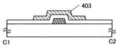
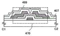
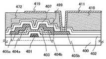
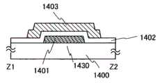
图2A是半导体器件中包含的薄膜晶体管470的平面图,以及图2B是沿图2A的线C1-C2所截取的截面图。薄膜晶体管470是反交错薄膜晶体管,并且在作为具有绝缘表面的衬底的衬底400之上包括栅电极层401、栅绝缘层402、氧化物半导体层403、源电极层405a和漏电极层405b。薄膜晶体管470覆盖有与氧化物半导体层403相接触的绝缘层407。保护绝缘层499层叠在绝缘层407之上。2A is a plan view of a
为了抑制薄膜晶体管470的电特性的变化,特意从氧化物半导体层中去除诸如氢、水分、羟基或氢化物(又称作氢化合物)之类的引起变化的杂质。另外,提供作为氧化物半导体的主成分并且在去除杂质的步骤中还原的氧。因此,得到电学上i型(本征)的高度纯化氧化物半导体层。这样,形成氧化物半导体层403。In order to suppress changes in the electrical characteristics of the
因此,优选的是,氧化物半导体层403中的氢尽可能比较少。氧化物半导体层403中包含的氢的浓度优选地设置为1×10¹⁶/cm3或更小,使得将氧化物半导体层403中包含的氢去除为尽可能接近零。Therefore, it is preferable that hydrogen in the
此外,高纯度氧化物半导体层403中的载流子的数量极小(接近零),并且载流子浓度小于1×10¹⁴/cm3,优选地小于1×1012 /cm3,更优选地为1×1011 /cm3或更小。由于氧化物半导体层403中的载流子的数量如此小,使得截止态电流能够在薄膜晶体管470中降低。截止态电流量越小则越好。薄膜晶体管470的沟道宽度(w)的每1 μm的电流值为100 aA/μm或更小,优选地为10 aA/μm或更小,更优选地为1 aA/μm或更小。此外,薄膜晶体管470没有pn结,并且没有被热载流子退化;因此,薄膜晶体管470的电特性没有受到pn结和退化影响。In addition, the number of carriers in the high-purity
为了降低诸如氢、水分、羟基或氢化物之类的杂质,在氧化物半导体层的形成之后,在氮气氛或者在诸如稀有气体(例如氩或氦)之类的惰性气体气氛中或者在降低的压力下、在暴露氧化物半导体层的状态中以200℃至700℃、优选地以350℃至700℃、更优选地以450℃至700℃来执行热处理(用于脱水或脱氢的热处理)。因此,降低氧化物半导体层中包含的水分。随后,在氧的气氛、氧和氮的气氛或者空气(超干空气)(露点优选地低于或等于-40℃,更优选地低于或等于-50℃)气氛中执行冷却。In order to reduce impurities such as hydrogen, moisture, hydroxyl groups, or hydrides, after the formation of the oxide semiconductor layer, in a nitrogen atmosphere or in an inert gas atmosphere such as a rare gas (such as argon or helium) or in a reduced Heat treatment (heat treatment for dehydration or dehydrogenation) is performed under pressure at 200°C to 700°C, preferably at 350°C to 700°C, more preferably at 450°C to 700°C in a state where the oxide semiconductor layer is exposed . Therefore, the moisture contained in the oxide semiconductor layer is reduced. Subsequently, cooling is performed in an atmosphere of oxygen, an atmosphere of oxygen and nitrogen, or air (ultra-dry air) (dew point preferably lower than or equal to -40°C, more preferably lower than or equal to -50°C).
作为脱水或脱氢处理,膜中包含的水分通过在氮气氛或惰性气体气氛或者在降低的压力下的热处理来降低。然后,作为用于提供氧的处理,在氧的气氛、氧和氮的气氛或者空气(超干空气)(露点优选地低于或等于-40℃,更优选地低于或等于-50℃)气氛中执行冷却。借助于这样得到的氧化物半导体层403,薄膜晶体管470的电特性得到改进。此外,能够实现能够大规模生产的具有高性能的薄膜晶体管。As dehydration or dehydrogenation treatment, moisture contained in the film is reduced by heat treatment in a nitrogen atmosphere or an inert gas atmosphere or under reduced pressure. Then, as a treatment for supplying oxygen, in an atmosphere of oxygen, an atmosphere of oxygen and nitrogen, or air (ultra-dry air) (the dew point is preferably lower than or equal to -40°C, more preferably lower than or equal to -50°C) Cooling is performed in atmosphere. With the
此外,降低了不仅在氧化物半导体层403而且还在栅绝缘层402以及氧化物半导体层403和设置成与其接触的上、下膜之间的界面(具体来说是氧化物半导体层403与栅绝缘层402之间的界面以及氧化物半导体层403与绝缘层407之间的界面)中存在的诸如水分之类的杂质。In addition, not only the
因此,为了可以尽可能少地包含氢、羟基和水分,优选的是,在形成栅绝缘层402和绝缘层407中脱附并且排出诸如氢或水分之类的杂质。此外,为了使脱附到衬底400的诸如氢或水分之类的杂质被脱附和排出,优选地在形成栅绝缘层402、氧化物半导体层403和绝缘层407之前执行预热。Therefore, in order that hydrogen, hydroxyl group, and moisture may be contained as little as possible, it is preferable to desorb and discharge impurities such as hydrogen or moisture in forming
包括沟道形成区的氧化物半导体层403可使用具有半导体特性的氧化物材料来形成。作为氧化物半导体层,能够使用任意下列氧化物半导体膜:诸如In-Sn-Ga-Zn-O膜之类的四元金属氧化物;诸如In-Ga-Zn-O膜、In-Sn-Zn-O膜、In-Al-Zn-O膜、Sn-Ga-Zn-O膜、Al-Ga-Zn-O膜和Sn-Al-Zn-O膜之类的三元金属氧化物;诸如In-Zn-O膜、Sn-Zn-O膜、Al-Zn-O膜、Zn-Mg-O膜、Sn-Mg-O膜或In-Mg-O膜之类的二元金属氧化物;In-O膜;Sn-O膜;Zn-O膜;或者能够使用类似的氧化物半导体。氧化物半导体膜可包含SiO2。The
作为氧化物半导体层,能够使用由InMO3(ZnO)m(m>0)所表示的薄膜。在这里,M表示从Ga、Al、Mn或Co中选取的一种或多种金属元素。例如,M能够是Ga、Ga和Al、Ga和Mn、Ga和Co等。其组成式由InMO3(ZnO)m(m>0)来表示、其中至少包含Ga作为M的氧化物半导体膜称作以上所述的In-Ga-Zn-O氧化物半导体,并且其薄膜又称作In-Ga-Zn-O膜。As the oxide semiconductor layer, a thin film represented by InMO3 (ZnO)m (m>0) can be used. Here, M represents one or more metal elements selected from Ga, Al, Mn or Co. For example, M can be Ga, Ga and Al, Ga and Mn, Ga and Co, and the like. An oxide semiconductor film whose composition formula is represented by InMO3 (ZnO)m (m > 0), in which at least Ga is contained as M, is called the above-mentioned In-Ga-Zn-O oxide semiconductor, and its thin film is also It is called an In-Ga-Zn-O film.
图40是包括背栅电极并且使用氧化物半导体的双栅薄膜晶体管的纵向截面图。氧化物半导体(OS)层隔着栅绝缘膜(GI)设置在栅电极(GE1)之上,并且源电极(S)和漏电极(D)设置在其之上。绝缘层设置成覆盖源电极(S)和漏电极(D)。背栅电极(GE2)设置在绝缘层之上与栅电极(GE1)重叠的区域中。40 is a longitudinal sectional view of a double-gate thin film transistor including a back gate electrode and using an oxide semiconductor. An oxide semiconductor (OS) layer is provided over the gate electrode (GE1) via a gate insulating film (GI), and a source electrode (S) and a drain electrode (D) are provided thereover. An insulating layer is provided to cover the source electrode (S) and the drain electrode (D). A back gate electrode (GE2) is disposed over the insulating layer in a region overlapping the gate electrode (GE1).
图41示出沿图40所示的A-A’截面的能带图(示意图)。图41中,黑点(●)表示电子,而白点表示空穴。图41示出其中正电压(VD>0)施加到漏电极但没有电压施加到栅电极(VG>0)的情况(由虚线示出)以及其中正电压(VD>0)施加到漏电极并且正电压(VG>0)施加到栅电极的情况(由实线示出)。当没有电压施加到栅电极时,载流子(电子)因高电位势垒而没有从电极注入到氧化物半导体侧,从而引起其中没有电流流动的截止态。相反,当正电压施加到栅极时,电位势垒降低,从而引起其中电流流动的导通态。FIG. 41 shows an energy band diagram (schematic diagram) along the AA' section shown in FIG. 40 . In FIG. 41, black dots (•) represent electrons, and white dots represent holes. Figure 41 shows the case (shown by dashed lines) where a positive voltage (VD >0) is applied to the drain electrode but no voltage is applied to the gate electrode (VG >0) and where a positive voltage (VD >0) is applied to The drain electrode and the case where a positive voltage (VG > 0) is applied to the gate electrode (shown by the solid line). When no voltage is applied to the gate electrode, carriers (electrons) are not injected from the electrode to the oxide semiconductor side due to a high potential barrier, causing an off state in which no current flows. Conversely, when a positive voltage is applied to the gate, the potential barrier is lowered, causing a conduction state in which current flows.
图42A和图42B是沿图40所示的B-B’截面的能带图(示意图)。图42A示出一种其中正电位(+VG)施加到栅电极(GE1)的状态,即,薄膜晶体管处于导通态的状态,其中载流子(电子)在源电极与漏电极之间流动。图42B示出其中负电位(-VG)施加到栅电极(GE1)的状态,即,其中薄膜晶体管处于截止态的情况(其中少数载流子没有流动的状态)。42A and 42B are energy band diagrams (schematic diagrams) along the BB' section shown in FIG. 40 . FIG. 42A shows a state in which a positive potential (+VG ) is applied to the gate electrode (GE1), that is, a state in which the thin film transistor is in an on state with carriers (electrons) between the source electrode and the drain electrode. flow. FIG. 42B shows a state in which a negative potential (-VG ) is applied to the gate electrode (GE1), that is, a case in which the thin film transistor is in an off state (a state in which minority carriers do not flow).
图43示出真空能级与金属的功函数(φM)之间的关系以及真空能级与氧化物半导体的电子亲合势(χ)之间的关系。FIG. 43 shows the relationship between the vacuum level and the work function (φM ) of the metal and the relationship between the vacuum level and the electron affinity (χ) of the oxide semiconductor.
在正常温度下,金属中的电子简并化,并且费米能级位于导带中。常规氧化物半导体层属于n型,并且费米能级(EF)在带隙的中间远离本征费米能级(Ei),并且位于更接近导带。注意,已知的是,氢的一部分是氧化物半导体中的施主,并且是使氧化物半导体作为n型半导体的一个因素。At normal temperatures, the electrons in metals are degenerate, and the Fermi level is located in the conduction band. A conventional oxide semiconductor layer belongs to the n type, and the Fermi level (EF ) is far from the intrinsic Fermi level (Ei ) in the middle of the band gap, and is located closer to the conduction band. Note that it is known that a part of hydrogen is a donor in an oxide semiconductor, and is a factor for making an oxide semiconductor an n-type semiconductor.
相反,按照本发明的氧化物半导体是通过从氧化物半导体中去除作为n型杂质的氢以及增加纯度以使得尽可能多地没有包含除了氧化物半导体的主要成分之外的杂质所得到的本征(i型)或基本上本征氧化物半导体膜。换言之,按照本发明的氧化物半导体是高度纯化的本征(i型)氧化物半导体膜或者不是通过添加杂质而是通过尽可能多地去除诸如氢、水、羟基或氢化物之类的杂质所得到的接近高度纯化的本征氧化物半导体膜的氧化物半导体膜。这样,费米能级(EF)能够处于与本征费米能级(Ei)相同的能级。In contrast, the oxide semiconductor according to the present invention is intrinsically obtained by removing hydrogen as an n-type impurity from the oxide semiconductor and increasing the purity so as not to contain impurities other than the main components of the oxide semiconductor as much as possible. (i-type) or substantially intrinsic oxide semiconductor film. In other words, the oxide semiconductor according to the present invention is a highly purified intrinsic (i-type) oxide semiconductor film or obtained not by adding impurities but by removing impurities such as hydrogen, water, hydroxyl groups, or hydrides as much as possible. The obtained oxide semiconductor film is close to a highly purified intrinsic oxide semiconductor film. In this way, the Fermi level (EF ) can be at the same energy level as the intrinsic Fermi level (Ei ).
据说,氧化物半导体的电子亲合势(χ)在其带隙(Eg)为3.15 eV的情况下为4.3 eV。源电极和漏电极中包含的钛(Ti)的功函数大致等于氧化物半导体的电子亲合势(χ)。在那种情况下,在金属与氧化物半导体之间的界面处没有形成肖特基电子势垒。It is said that the electron affinity (χ) of an oxide semiconductor is 4.3 eV when its band gap (Eg ) is 3.15 eV. The work function of titanium (Ti) contained in the source electrode and the drain electrode is approximately equal to the electron affinity (χ) of the oxide semiconductor. In that case, no Schottky electron barrier is formed at the interface between the metal and the oxide semiconductor.
在这种情况下,如图42A所示,电子沿栅绝缘膜与高纯度氧化物半导体之间的界面处的能量上稳定的氧化物半导体的最低部分移动。In this case, as shown in FIG. 42A , electrons move along the lowest portion of the energetically stable oxide semiconductor at the interface between the gate insulating film and the high-purity oxide semiconductor.
图42B中,当负电位施加到栅电极(GE1)时,作为少数载流子的空穴的数量大致为零;因此,电流值变为尽可能接近零的值。In FIG. 42B, when a negative potential is applied to the gate electrode (GE1), the number of holes as minority carriers is approximately zero; therefore, the current value becomes a value as close to zero as possible.
例如,甚至当薄膜晶体管具有1×104 μm的沟道宽度W以及3 μm的沟道长度时,也能够得到10-13 A或更低的截止态电流以及0.1 V/dec.的亚阈值(S值)(栅绝缘膜的厚度为100 nm)。For example, even when a thin film transistor has a channel width W of 1×104 μm and a channel length of 3 μm, an off-state current of 10−13 A or less and a subthreshold of 0.1 V/dec. ( S value) (the thickness of the gate insulating film is 100 nm).
如上所述,氧化物半导体经过高度纯化,使得尽可能少地包含除了氧化物半导体的主要成分之外的杂质,由此能够得到薄膜晶体管的有利操作。As described above, the oxide semiconductor is highly purified so that impurities other than the main components of the oxide semiconductor are contained as little as possible, whereby favorable operation of the thin film transistor can be obtained.
虽然使用作为薄膜晶体管470的单栅薄膜晶体管来给出描述,但是可根据需要形成包括多个沟道形成区的多栅薄膜晶体管。Although the description has been given using a single-gate thin film transistor as the
在这个实施例中,包含In-Ga-Zn-O的半导体膜用作氧化物半导体层403。In this embodiment, a semiconductor film containing In-Ga-Zn-O is used as the
图1A至图1D是示出图2A和图2B所示的薄膜晶体管470的制造工序的截面图。1A to 1D are cross-sectional views showing the manufacturing process of the
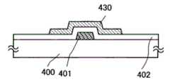
图1A中,栅电极层401设置在作为具有绝缘表面的衬底的衬底400之上。所形成的栅电极的边缘部分优选地具有渐窄的形状,因为其上层叠的栅绝缘层的覆盖率能够得到改进。注意,抗蚀剂掩模可通过喷墨方法来形成。通过喷墨方法来形成抗蚀剂掩模不需要光掩模;因此,制造成本能够降低。In FIG. 1A, a
虽然对于能够用作具有绝缘表面的衬底400的衬底没有具体限制,然而必要的是,衬底至少具有耐受后来执行的热处理的充分耐热性。例如,能够使用采用钡硼硅酸盐玻璃、铝硼硅酸盐玻璃等等所形成的玻璃衬底。Although there is no particular limitation on the substrate that can be used as the
在使用玻璃衬底并且用以后来执行热处理的温度较高的情况下,优选地使用其应变点大于或等于730℃的玻璃衬底。作为玻璃衬底,例如使用诸如铝硅酸盐玻璃、铝硼硅酸盐玻璃或钡硼硅酸盐玻璃之类的玻璃材料。注意,通过包含比氧化硼更大量的氧化钡(BaO),得到更实用的耐热玻璃衬底。因此,优选地使用包含使得BaO的量比B2O3要大的BaO和B2O3的玻璃衬底。In the case where a glass substrate is used and the temperature at which heat treatment is performed later is high, it is preferable to use a glass substrate whose strain point is greater than or equal to 730°C. As the glass substrate, for example, a glass material such as aluminosilicate glass, aluminoborosilicate glass or barium borosilicate glass is used. Note that by including a larger amount of barium oxide (BaO) than boron oxide, a more practical heat-resistant glass substrate is obtained. Therefore, it is preferable to use a glass substrate containing BaO and B2 O3 such that the amount of BaO is larger than that of B2 O3 .
注意,作为上述玻璃衬底,可使用采用诸如陶瓷衬底、石英衬底或蓝宝石衬底之类的绝缘体所形成的衬底。备选地,可使用晶化玻璃等。又备选地,能够适当地使用塑料衬底等。Note that, as the above-mentioned glass substrate, a substrate formed using an insulator such as a ceramic substrate, a quartz substrate, or a sapphire substrate can be used. Alternatively, crystallized glass or the like can be used. Still alternatively, a plastic substrate or the like can be suitably used.
用作基底膜的绝缘膜可设置在衬底400与栅电极层401之间。基底膜具有防止杂质元素从衬底400扩散的功能,并且能够形成为具有使用氮化硅膜、氧化硅膜、氮氧化硅膜和氧氮化硅膜中的一个或多个的单层结构或分层结构。An insulating film serving as a base film may be provided between the
栅电极层401能够在使用诸如钼、钛、铬、钽、钨、铝、铜、钕或钪之类的金属材料或者包含这些材料的任一种作为主要成分的合金材料的单层或叠层中形成。The
例如,作为栅电极层401的二层结构,下列结构是优选的:铝层以及层叠在其上的钼层的二层结构,铜层以及层叠在其上的钼层的二层结构,铜层以及层叠在其上的氮化钛层或氮化钽层的二层结构,以及氮化钛层和钼层的二层结构。作为三层结构,钨层或氮化钨层、铝和硅的合金或者铝和钛的合金层以及氮化钛层或钛层的层叠结构是优选的。注意,栅电极层能够使用具有透光性质的导电膜来形成。作为具有透光性质的导电膜的一个示例,能够给出透明导电氧化物等。For example, as the two-layer structure of the
随后,栅绝缘层402在栅电极层401之上形成。Subsequently, a
栅绝缘层402能够通过等离子体CVD方法、溅射方法等等形成为具有使用氧化硅层、氮化硅层、氧氮化硅层、氮氧化硅层、氧化铝层、氮化铝层、氧氮化铝层、氮氧化铝层和氧化铪层的任一个的单层结构或分层结构。注意,优选的是,栅绝缘层402中没有包含大量氢。在氧化硅膜通过溅射方法来形成的情况下,硅靶或石英靶用作靶,并且氧气体或者氧和氩的混合气体用作溅射气体。The
栅绝缘层402可具有一种结构,其中从栅电极层401侧来层叠氮化硅层和氧化硅层。例如,通过溅射方法来形成作为第一栅绝缘层的厚度为50 nm至200 nm(包括两端)的氮化硅层(SiNy(y>0)),并且在第一栅绝缘层之上层叠作为第二栅绝缘层的厚度为5 nm至300 nm(包括两端)的氧化硅层(SiOx(x>0));这样,形成厚度为100 nm的栅绝缘层。栅绝缘层402的厚度可根据薄膜晶体管所需的特性来适当设置,并且可以是大约350 nm至400 nm。The
此外,为了可能在栅绝缘层402和氧化物半导体膜中尽可能少地包含氢、羟基和水分,优选的是,其上形成栅电极层401的衬底400或者其上形成直到栅绝缘层402的层的衬底400在溅射设备的预热室中经过预热作为用于膜形成的预处理,使得脱附和排出吸附于衬底400的诸如氢和水分之类的杂质。注意,作为排空单元,低温泵优选地设置在预热室中。还要注意,这种预热处理在一些情况下能够省略。此外,这种预热可类似地在形成绝缘层407之前对其上形成了直到源电极层405a和漏电极层405b的层的衬底400来执行。In addition, in order to contain hydrogen, hydroxyl groups, and moisture as little as possible in the
然后,氧化物半导体膜在栅绝缘层402之上形成为2 nm至200 nm(包括两端)的厚度。Then, an oxide semiconductor film is formed to a thickness of 2 nm to 200 nm (both inclusive) over the
注意,在氧化物半导体膜通过溅射方法来形成之前,栅绝缘层402的表面上的灰尘优选地通过其中引入氩气体并且生成等离子体的反向溅射被去除。反向溅射指的是一种方法,其中,在没有将电压施加到靶侧的情况下,RF电源用于在氩气氛中将电压施加到衬底侧,使得等离子体在衬底附近生成,以便修正表面。注意,代替氩气氛,可使用氮气氛、氦气氛、氧气氛等。Note that before the oxide semiconductor film is formed by a sputtering method, dust on the surface of the
氧化物半导体膜通过溅射方法来形成。作为氧化物半导体膜,能够使用任意下列氧化物半导体膜:诸如In-Sn-Ga-Zn-O膜之类的四元金属氧化物;诸如In-Ga-Zn-O膜、In-Sn-Zn-O膜、In-Al-Zn-O膜、Sn-Ga-Zn-O膜、Al-Ga-Zn-O膜和Sn-Al-Zn-O膜之类的三元金属氧化物;诸如In-Zn-O膜、Sn-Zn-O膜、Al-Zn-O膜、Zn-Mg-O膜、Sn-Mg-O膜或In-Mg-O膜之类的二元金属氧化物;In-O膜;Sn-O膜;Zn-O膜;等等。在这个实施例中,氧化物半导体膜通过溅射方法、借助于In-Ga-Zn-O基氧化物半导体膜形成靶来形成。氧化物半导体膜能够通过溅射方法在稀有气体(通常为氩)气氛、氧气氛或者稀有气体(通常为氩)和氧的气氛中形成。在使用溅射方法的情况下,包含2 wt%至10 wt%(包括两端)的SiO2的靶可用于膜形成。The oxide semiconductor film is formed by a sputtering method. As the oxide semiconductor film, any of the following oxide semiconductor films can be used: quaternary metal oxides such as In-Sn-Ga-Zn-O films; Ternary metal oxides such as -O film, In-Al-Zn-O film, Sn-Ga-Zn-O film, Al-Ga-Zn-O film and Sn-Al-Zn-O film; such as In - Binary metal oxides such as Zn-O film, Sn-Zn-O film, Al-Zn-O film, Zn-Mg-O film, Sn-Mg-O film or In-Mg-O film; In -O film; Sn-O film; Zn-O film; etc. In this embodiment, an oxide semiconductor film is formed by a sputtering method by means of an In-Ga-Zn-O-based oxide semiconductor film-forming target. The oxide semiconductor film can be formed by a sputtering method in a rare gas (usually argon) atmosphere, an oxygen atmosphere, or a rare gas (usually argon) and oxygen atmosphere. In the case of using the sputtering method, a target containing 2 wt % to 10 wt % (both inclusive) of SiO2 can be used for film formation.
作为用于形成氧化物半导体膜的溅射气体,优选地使用高纯度气体,其中诸如氢、水、羟基或氢化物之类的杂质降低到杂质浓度级由单位“ppm”或“ppb”来表示的程度。As a sputtering gas for forming an oxide semiconductor film, it is preferable to use a high-purity gas in which impurities such as hydrogen, water, hydroxyl groups, or hydrides are reduced to an impurity concentration level expressed by the unit "ppm" or "ppb" Degree.
作为用于通过溅射方法来形成氧化物半导体膜的靶,能够使用包含氧化锌作为其主要成分的金属氧化物的靶。作为金属氧化物靶的另一个示例,能够使用包含In、Ga和Zn的氧化物半导体膜形成靶(其中组成比为In2O3:Ga2O3:ZnO=1:1:1 [摩尔比],In:Ga:Zn=1:1:0.5 [原子比])。作为包含In、Ga和Zn的氧化物半导体膜形成靶,能够使用组成比为In:Ga:Zn=1:1:1 [原子比]或In:Ga:Zn=1:1:2[原子比]的靶。氧化物半导体膜形成靶的填充率为90%至100%(包括两端),优选地为95%至99.9%(包括两端)。通过使用具有高填充率的氧化物半导体膜形成靶,所形成的氧化物半导体膜成为密集膜。As a target for forming an oxide semiconductor film by a sputtering method, a target of a metal oxide containing zinc oxide as its main component can be used. As another example of the metal oxide target, an oxide semiconductor film formation target containing In, Ga, and Zn (wherein the composition ratio is In2 O3 :Ga2 O3 :ZnO=1:1:1 [molar ratio ], In:Ga:Zn=1:1:0.5 [atomic ratio]). As an oxide semiconductor film formation target containing In, Ga, and Zn, a composition ratio of In:Ga:Zn=1:1:1 [atomic ratio] or In:Ga:Zn=1:1:2 [atomic ratio] can be used. ] target. The filling rate of the oxide semiconductor film formation target is 90% to 100% (both inclusive), preferably 95% to 99.9% (both inclusive). By using an oxide semiconductor film formation target having a high filling factor, the formed oxide semiconductor film becomes a dense film.
衬底保持在控制为降低的压力的处理室中,并且衬底温度设置为100℃至600℃(包括两端)、优选地为200℃至400℃(包括两端)。膜形成在加热衬底的同时执行,由此所形成的氧化物半导体膜中包含的杂质的浓度能够降低。另外,通过溅射引起的损坏能够减小。在去除处理室中剩余的水分的同时,引入去除了氢和水分的溅射气体,以便使用金属氧化物作为靶在衬底400之上形成氧化物半导体膜。为了去除处理室中的剩余水分,优选地使用吸附真空泵。例如,优选地使用低温泵、离子泵或钛升华泵。排空单元能够是提供有冷阱的涡轮泵。从借助于低温泵执行了排空的沉积室,例如,排出氢原子、诸如水(H2O)之类的包含氢原子的化合物(更优选地还有包含碳原子的化合物)等;因此,在沉积室中形成的氧化物半导体膜中包含的杂质的浓度能够降低。The substrate is kept in a process chamber controlled to a reduced pressure, and the substrate temperature is set at 100°C to 600°C inclusive, preferably 200°C to 400°C inclusive. Film formation is performed while heating the substrate, whereby the concentration of impurities contained in the formed oxide semiconductor film can be reduced. In addition, damage caused by sputtering can be reduced. While removing moisture remaining in the process chamber, a sputtering gas from which hydrogen and moisture are removed is introduced to form an oxide semiconductor film over the
在形成氧化物半导体膜的情况下,优选地使用诸如低温泵之类的排空单元,以便防止在形成与氧化物半导体膜相接触的膜之前和之后的步骤中以及在形成氧化物半导体膜之前和之后的步骤中混入处理室中(不用说,包括用于形成氧化物半导体膜的处理室)作为杂质的剩余水分。In the case of forming an oxide semiconductor film, an evacuation unit such as a cryopump is preferably used in order to prevent the and residual moisture mixed in the processing chamber (including, needless to say, the processing chamber for forming the oxide semiconductor film) as impurities in the subsequent steps.
作为膜形成条件的一个示例,衬底与靶之间的距离为100 mm,压力为0.6 Pa,直流(DC)电源为0.5 kW,以及气氛为氧气氛(氧流率的比例为100%)。优选的是使用脉冲直流(DC)电源,因为能够降低粉状物质(又称作粒子或灰尘),并且膜厚度能够是均匀的。氧化物半导体膜的厚度优选地为5 nm至30 nm(包括两端)。由于适当厚度取决于所使用的氧化物半导体材料,所以厚度能够根据材料来适当地确定。As an example of film formation conditions, the distance between the substrate and the target is 100 mm, the pressure is 0.6 Pa, the direct current (DC) power supply is 0.5 kW, and the atmosphere is an oxygen atmosphere (the ratio of the oxygen flow rate is 100%). It is preferable to use a pulsed direct current (DC) power supply because powdery matter (also known as particles or dust) can be reduced and the film thickness can be uniform. The thickness of the oxide semiconductor film is preferably 5 nm to 30 nm (both inclusive). Since an appropriate thickness depends on the oxide semiconductor material used, the thickness can be appropriately determined according to the material.
溅射方法的示例包括:RF溅射方法,其中高频电力用于溅射电源;DC溅射方法;以及脉冲DC溅射方法,其中以脉冲方式来施加偏压。RF溅射方法主要用于形成绝缘膜的情况,而DC溅射方法主要用于形成金属膜的情况。Examples of the sputtering method include: an RF sputtering method in which high-frequency power is used for a sputtering power source; a DC sputtering method; and a pulsed DC sputtering method in which a bias voltage is applied in a pulsed manner. The RF sputtering method is mainly used in the case of forming an insulating film, and the DC sputtering method is mainly used in the case of forming a metal film.
另外,还存在多源溅射设备,其中能够设置不同材料的多个靶。通过多源溅射设备,不同材料的膜能够形成为层叠在同一室中,或者多种材料的膜能够通过在同一室中同时放电来形成。In addition, there are also multi-source sputtering devices in which a plurality of targets of different materials can be set. With a multi-source sputtering apparatus, films of different materials can be formed to be laminated in the same chamber, or films of a plurality of materials can be formed by simultaneous discharge in the same chamber.
备选地,能够使用提供有室内部的磁体系统并且用于磁控管溅射方法的溅射设备或者用于ECR溅射方法、其中使用借助于微波所生成的等离子体而没有使用辉光放电的溅射设备。Alternatively, it is possible to use a sputtering device provided with a magnet system inside the chamber and used for a magnetron sputtering method or for an ECR sputtering method in which a plasma generated by means of microwaves is used without using a glow discharge sputtering equipment.
此外,作为使用溅射方法的膜形成方法,能够使用其中靶物质和溅射气体成分在膜形成期间相互起化学反应以形成其化合物薄膜的反应溅射方法或者其中电压在膜形成期间还施加到衬底的偏压溅射方法。In addition, as a film forming method using a sputtering method, it is possible to use a reactive sputtering method in which a target substance and sputtering gas components chemically react with each other during film formation to form a compound thin film thereof or in which a voltage is also applied to Substrate bias sputtering method.
然后,通过光刻步骤将氧化物半导体膜处理成岛状氧化物半导体层430(参见图1A)。用于形成岛状氧化物半导体层430的抗蚀剂掩模可使用喷墨方法来形成。通过喷墨方法来形成抗蚀剂掩模不需要光掩模;因此,制造成本能够降低。Then, the oxide semiconductor film is processed into an island-shaped
注意,氧化物半导体膜的蚀刻可以是干式蚀刻,而无需局限于湿式蚀刻。Note that etching of the oxide semiconductor film may be dry etching without being limited to wet etching.
蚀刻条件(例如蚀刻剂、蚀刻时间和温度)根据材料来适当地调整,使得材料能够蚀刻成预期形状。Etching conditions such as etchant, etching time, and temperature are appropriately adjusted according to the material so that the material can be etched into a desired shape.
在栅绝缘层402中形成接触孔的情况下,可在形成氧化物半导体层430中执行该步骤。This step may be performed in forming the
为了降低诸如氢、水分、羟基或氢化物之类的杂质,在氮气氛或者诸如稀有气体(例如氩或氦)之类的惰性气体气氛中或者在降低的压力下以200℃至700℃(或者衬底的应变点)、优选地以350℃至700℃、更优选地以450℃至700℃来对氧化物半导体层430执行热处理(用于脱水或脱氢的热处理,又称作第一热处理)。因此,减少氧化物半导体层中包含的水分。In order to reduce impurities such as hydrogen, moisture, hydroxyl groups, or hydrides, in a nitrogen atmosphere or an inert gas atmosphere such as a rare gas (such as argon or helium) or under reduced pressure at 200°C to 700°C (or strain point of the substrate), preferably at 350° C. to 700° C., more preferably at 450° C. to 700° C., to perform heat treatment on the oxide semiconductor layer 430 (heat treatment for dehydration or dehydrogenation, also referred to as first heat treatment ). Therefore, moisture contained in the oxide semiconductor layer is reduced.
随后,在氧的气氛、氧和氮的气氛或者空气(露点优选地低于或等于-40℃,更优选地低于或等于-50℃)气氛中冷却氧化物半导体层。这样,得到高度纯化的i型(本征)氧化物半导体层。因此,得到电学上i型(本征)的高度纯化氧化物半导体膜。这样,形成氧化物半导体层403(参见图1B)。Subsequently, the oxide semiconductor layer is cooled in an atmosphere of oxygen, an atmosphere of oxygen and nitrogen, or an atmosphere of air (the dew point is preferably lower than or equal to -40°C, more preferably lower than or equal to -50°C). In this way, a highly purified i-type (intrinsic) oxide semiconductor layer is obtained. Thus, an electrically i-type (intrinsic) highly purified oxide semiconductor film is obtained. In this way, the
对氧化物半导体(IGZO)表面的氧的吸附能量通过第一原理计算来计算。注意,由Accelrys Software Inc.生产的第一原理计算的软件CASTEP用于第一原理计算。通过从O2的内能与IGZO的内能之和(E(O2)+E(IGZO))中减去O2吸附到其中的IGZO的内能,来确定吸附能量(Ead),即,吸附能量(Ead)定义为Ead=(E(O2)+E(IGZO))-E(O2吸附到其中的IGZO)。计算结果表明,氧的吸附是放热反应,并且放热能量为1.46 eV。The adsorption energy of oxygen on the surface of the oxide semiconductor (IGZO) was calculated by first-principles calculation. Note that CASTEP, a software for first-principle calculation produced by Accelrys Software Inc., was used for the first-principle calculation. The adsorption energy (Ead ) was determined by subtracting the internal energy of IGZO into whichO2 was adsorbed, from the sum of the internal energy ofO2 and that of IGZO (E(O2 )+E(IGZO)), i.e. , the adsorption energy (Ead ) is defined as Ead =(E(O2 )+E(IGZO))−E(IGZO into which O2 is adsorbed). The calculation results show that the adsorption of oxygen is an exothermic reaction, and the exothermic energy is 1.46 eV.
当氢分子存在时,氢分子与氧分子之间的氧化反应、即表示为“2H2+O2→2H2O”的氧化反应因用于脱水或脱氢的热处理而可能发生。如果通过氧的吸附所得到的能量用于氧化反应并且因而氧化反应发生,则存在H2不能离开IGZO并且可能保留在IGZO中的问题。因此,无法对IGZO执行充分脱水或脱氢处理。When hydrogen molecules exist, an oxidation reaction between hydrogen molecules and oxygen molecules, that is, an oxidation reaction expressed as "2H2 +O2 →2H2 O", may occur due to heat treatment for dehydration or dehydrogenation. If the energy obtained by the adsorption of oxygen is used for the oxidation reaction and thus the oxidation reaction takes place, there is a problem thatH cannot leave the IGZO and may remain in the IGZO. Therefore, sufficient dehydration or dehydrogenation treatment cannot be performed on IGZO.
因此,为了防止产生水的反应,优选的是通过下列过程来形成电学上i型的高度纯化氧化物半导体层:通过在氮气氛或者诸如稀有气体(例如氩或氦)之类的惰性气体气氛中或者在降低的压力下对氧化物半导体层执行脱水或脱氢处理,然后在氧的气氛或者空气(露点优选地低于或等于-40℃,更优选地低于或等于-50℃)气氛中执行冷却,以便提供作为氧化物半导体的主要成分的氧。Therefore, in order to prevent a water-generating reaction, it is preferable to form an electrically i-type highly purified oxide semiconductor layer by forming an electrically i-type highly purified oxide semiconductor layer in a nitrogen atmosphere or an inert gas atmosphere such as a rare gas (eg, argon or helium). Or dehydration or dehydrogenation treatment is performed on the oxide semiconductor layer under reduced pressure, and then in an atmosphere of oxygen or air (the dew point is preferably lower than or equal to -40°C, more preferably lower than or equal to -50°C) Cooling is performed so as to supply oxygen as a main component of the oxide semiconductor.
在这个实施例中,将衬底引入作为一种热处理设备的电炉中,在氮气氛中以450℃对氧化物半导体层执行一小时热处理,并且在氧气氛中执行冷却。In this embodiment, the substrate was introduced into an electric furnace as a heat treatment device, heat treatment was performed on the oxide semiconductor layer at 450° C. for one hour in a nitrogen atmosphere, and cooling was performed in an oxygen atmosphere.
本发明的一个特征是使氧化物半导体层经过在氮气氛或者诸如稀有气体(例如氩或氦)之类的惰性气体气氛中或者在降低的压力下的用于脱水或脱氢处理的热处理以及经过在氧的气氛、氧和氮的气氛或者空气(露点优选地低于或等于-40℃,更优选地低于或等于-50℃)气氛中的用于提供氧的处理的冷却步骤。A feature of the present invention is to subject the oxide semiconductor layer to heat treatment for dehydration or dehydrogenation treatment in a nitrogen atmosphere or an inert gas atmosphere such as a rare gas (for example, argon or helium) or under reduced pressure and to undergo A cooling step for the treatment to provide oxygen in an atmosphere of oxygen, an atmosphere of oxygen and nitrogen, or an atmosphere of air (dew point preferably lower than or equal to -40°C, more preferably lower than or equal to -50°C).
脱水或脱氢处理以及用于提供氧的处理中的氧化物半导体层(和衬底)的温度状态是上升状态、恒定状态和下降状态。气体(气氛)可在下列定时的任一个从氮或者诸如稀有气体(例如氩或氦)之类的惰性气体切换到氧和氮或者空气(露点优选地低于或等于-40℃,更优选地低于或等于-50℃):在氧化物半导体层的温度处于恒定状态的时候,在氧化物半导体层的温度下降开始的时候,以及在氧化物半导体层的温度处于下降状态的时候。The temperature states of the oxide semiconductor layer (and the substrate) in the dehydration or dehydrogenation treatment and the treatment for supplying oxygen are a rising state, a constant state, and a falling state. The gas (atmosphere) can be switched from nitrogen or an inert gas such as a rare gas (eg argon or helium) to oxygen and nitrogen or air (dew point preferably lower than or equal to -40°C, more preferably lower than or equal to -50° C.): when the temperature of the oxide semiconductor layer is in a constant state, when the temperature drop of the oxide semiconductor layer starts, and when the temperature of the oxide semiconductor layer is in a falling state.
注意,热处理设备并不局限于电炉,而是可包括用于通过来自诸如电阻加热元件之类的加热元件的热传导或热辐射来加热待处理对象的任何装置。例如,能够使用诸如GRTA(气体快速热退火)设备或LRTA(灯快速热退火)设备之类的RTA(快速热退火)设备。LRTA设备是用于通过从诸如卤素灯、金属卤化物灯、氙弧灯、碳弧灯、高压钠灯或高压水银灯之类的灯所发射的光(电磁波)的辐射来加热待处理对象的设备。GRTA设备是用于使用高温气体的热处理的设备。作为气体,使用诸如氮之类或者诸如氩之类的稀有气体等的不会通过热处理来与待处理对象发生反应的惰性气体。Note that the heat treatment apparatus is not limited to an electric furnace, but may include any device for heating an object to be treated by heat conduction or heat radiation from a heating element such as a resistance heating element. For example, RTA (rapid thermal annealing) equipment such as GRTA (gas rapid thermal annealing) equipment or LRTA (lamp rapid thermal annealing) equipment can be used. The LRTA apparatus is an apparatus for heating an object to be treated by radiation of light (electromagnetic waves) emitted from a lamp such as a halogen lamp, metal halide lamp, xenon arc lamp, carbon arc lamp, high-pressure sodium lamp, or high-pressure mercury lamp. GRTA equipment is equipment used for heat treatment using high-temperature gas. As the gas, an inert gas that does not react with an object to be processed by heat treatment such as nitrogen or a rare gas such as argon is used.
例如,用于脱水或脱氢的热处理能够采用GRTA,其中将衬底移入加热到650℃至700℃的高温的惰性气体中,并且在其中加热数分钟,然后将衬底移出加热到高温的惰性气体。通过GRTA,能够实现短时间段的高温热处理。For example, heat treatment for dehydration or dehydrogenation can employ GRTA, in which the substrate is moved into an inert gas heated to a high temperature of 650°C to 700°C and heated therein for several minutes, and then the substrate is moved out of the inert gas heated to a high temperature. gas. By GRTA, high-temperature heat treatment for a short period of time can be realized.
注意,优选的是,在用于脱水或脱氢处理的热处理中,诸如氢、水分、羟基或氢化物之类的杂质没有包含在氮或者诸如氦、氖或氩之类的惰性气体中。优选的是,引入热处理设备中的氮或者诸如氦、氖或氩之类的稀有气体的纯度为6N(99.9999%)或更高、优选地为7N(99.99999%)或更高(也就是说,杂质浓度为1 ppm或更低,优选地为0.1 ppm或更低)。Note that it is preferable that impurities such as hydrogen, moisture, hydroxyl groups or hydrides are not contained in nitrogen or an inert gas such as helium, neon or argon in heat treatment for dehydration or dehydrogenation treatment. It is preferable that nitrogen or a rare gas such as helium, neon or argon introduced into the heat treatment apparatus has a purity of 6N (99.9999%) or higher, preferably 7N (99.99999%) or higher (that is, The impurity concentration is 1 ppm or less, preferably 0.1 ppm or less).
在这里,使用电炉601的加热方法参照图3描述为氧化物半导体层430的热处理的一种模式。Here, the heating method using the
图3是电炉601的示意图。加热器603设置在室602外部,并且加热室602。在室602内部,设置了其中设置衬底604的基座605。向/从室602传递衬底604。另外,室602提供有气体供应单元606和排空单元607。通过气体供应单元606,将气体引入室602中。排空单元607排空室602的内部,或者降低室602中的压力。注意,电炉601的温度上升特性优选地设置为从0.1℃/min至20℃/min。电炉601的温度降低特性优选地设置为从0.1℃/min至15℃/min。FIG. 3 is a schematic diagram of an
气体供应单元606包括气体供应源611a、气体供应源611b、压力调整阀612a、压力调整阀612b、提纯设备613a、提纯设备613b、质量流控制器(mass flow controller)614a、质量流控制器614b、截止阀615a和截止阀615b。在这个实施例中,优选的是,提纯设备613a和提纯设备613b设置在气体供应源611a和611b与室602之间。通过提纯设备613a和提纯设备613b,从气体供应源611a和气体供应源611b引入室602的气体中的诸如氢、水分、羟基或氢化物之类的杂质能够由提纯设备613a和提纯设备613b去除,使得能够抑制诸如氢、水分、羟基或氢化物之类的杂质进入室602。The
在这个实施例中,氮或稀有气体从气体供应源611a和气体供应源611b引入室602,使得室的内部设置为氮或稀有气体气氛。在加热到200℃至700℃(或者衬底604的应变点)、优选地为350℃至700℃、更优选地为450℃至700℃的温度的室602中,加热在衬底604之上形成的氧化物半导体层430,由此氧化物半导体层430能够脱水或脱氢。In this embodiment, nitrogen or a rare gas is introduced into the
备选地,以200℃至700℃(或者衬底604的应变点)、优选地以350℃至700℃、更优选地以450℃至700℃来加热由排空单元降低了压力的室602。在这种室602中,加热在衬底604之上形成的氧化物半导体层430,由此氧化物半导体层430能够经过脱水或脱氢。Alternatively, the
随后,停止将氮或稀有气体从气体供应源611a引入室602,并且关断加热器。然后,氧或者氧和氮从气体供应源611b引入室602中,并且缓慢地冷却加热设备的室602。也就是说,室602的内部设置成氧气氛,并且缓慢地冷却衬底604。在这里,优选的是,从气体供应源611b引入室602的氧没有包含诸如水和氢之类的杂质。另外,优选的是,从气体供应源611b引入室602的氧的纯度为6N(99.9999%)或更低、优选地为7N(99.99999%)(即,氧的杂质浓度为1 ppm,优选地为0.1 ppm)或更低。Subsequently, introduction of nitrogen or a rare gas from the
虽然在空气气氛而不是氧的气氛或者氧和氮的气氛中对氧化物半导体层执行冷却,但是优选的是,诸如水和氢之类的杂质没有包含在引入室602的空气中,并且使用露点优选地低于或等于-40℃、更优选地低于或等于-50℃的超干空气。Although the cooling of the oxide semiconductor layer is performed in an air atmosphere instead of an oxygen atmosphere or an oxygen and nitrogen atmosphere, it is preferable that impurities such as water and hydrogen are not contained in the air introduced into the
氧化物半导体层被加热以经过脱水或脱氢,并且在氧的气氛、氧和氮的气氛或者空气(露点优选地低于或等于-40℃,更优选地低于或等于-50℃)气氛中冷却氧化物半导体层。因此,得到电学上i型(本征)的高度纯化氧化物半导体膜。这样,能够形成氧化物半导体层403。The oxide semiconductor layer is heated to undergo dehydration or dehydrogenation, and is heated in an atmosphere of oxygen, an atmosphere of oxygen and nitrogen, or an atmosphere of air (the dew point is preferably lower than or equal to -40°C, more preferably lower than or equal to -50°C). cooling the oxide semiconductor layer. Thus, an electrically i-type (intrinsic) highly purified oxide semiconductor film is obtained. In this way, the
注意,关断用于加热室602的加热器的定时可与氧或稀有气体与氧、氧和氮或者空气气氛之间的切换定时是相同的。氮或稀有气体与氧、氧和氮或空气气氛之间的切换定时可比关断加热器的定时更早或更迟,只要在脱水或脱氢处理之后执行切换。Note that the timing of turning off the heater for heating the
因此,后来完成的薄膜晶体管的可靠性能够得到提高。Therefore, the reliability of a thin film transistor completed later can be improved.
注意,在降低的压力下执行热处理的情况下,氧和氮或空气气氛(超干空气)可在热处理之后引入室602中,压力可返回到大气压力,然后执行冷却。Note that in the case of performing heat treatment under reduced pressure, oxygen and nitrogen or an air atmosphere (ultra dry air) may be introduced into the
另外,当氧从气体供应源611b引入室602时,氮和诸如氦、氖或氩之类的稀有气体中的一个或两者可引入室602。Additionally, one or both of nitrogen and a rare gas such as helium, neon, or argon may be introduced into the
如果加热设备具有多室结构,则热处理和冷却处理能够在不同室中执行。通常,在填充有氮或稀有气体并且以200℃至700℃(或者衬底604的应变点)、优选地以350℃至700℃、更优选地以450℃至700℃加热的第一室中加热衬底之上的氧化物半导体层。随后,通过引入了氮或稀有气体的传递室,经过了热处理的衬底移入填充有氧、氧和氮或空气气氛(超干空气)的第二室,并且执行冷却处理。通过这些步骤,产量能够提高。If the heating device has a multi-chamber structure, heat treatment and cooling treatment can be performed in different chambers. Typically, in a first chamber filled with nitrogen or a noble gas and heated at 200°C to 700°C (or the strain point of the substrate 604), preferably at 350°C to 700°C, more preferably at 450°C to 700°C The oxide semiconductor layer over the substrate is heated. Subsequently, through the transfer chamber into which nitrogen or a rare gas is introduced, the heat-treated substrate is moved into a second chamber filled with oxygen, oxygen and nitrogen, or an air atmosphere (ultra-dry air), and cooling treatment is performed. Through these steps, yield can be improved.
此外,用于提供氧的处理以及用于氧化物半导体层的脱水或脱氢处理的热处理可对尚未处理成岛状氧化物半导体层的氧化物半导体膜执行。在那种情况下,在用于脱水或脱氢处理的热处理以及用于提供氧的处理之后,从处理设备中取出衬底,并且执行光刻步骤。In addition, treatment for supplying oxygen and heat treatment for dehydration or dehydrogenation treatment of the oxide semiconductor layer may be performed on the oxide semiconductor film that has not been processed into the island-shaped oxide semiconductor layer. In that case, after heat treatment for dehydration or dehydrogenation treatment and treatment for supplying oxygen, the substrate is taken out from the processing apparatus, and a photolithography step is performed.
对氧化物半导体层具有脱水或脱氢的作用的热处理可在下列定时的任一个执行:在形成氧化物半导体层之后;以及在源电极和漏电极层叠在氧化物半导体层之上之后。The heat treatment having a dehydration or dehydrogenation effect on the oxide semiconductor layer may be performed at any one of the following timings: after the oxide semiconductor layer is formed; and after the source electrode and the drain electrode are stacked over the oxide semiconductor layer.
此外,在栅绝缘层402中形成接触孔的情况下,该步骤可在对氧化物半导体层430执行脱水或脱氢处理之前或之后执行。Also, in the case of forming a contact hole in the
随后,将要作为源电极层和漏电极层(包括在与源电极层和漏电极层相同的层中形成的布线)的导电膜在栅绝缘层402和氧化物半导体层403之上形成。导电膜可通过溅射方法或真空蒸镀方法来形成。作为将要成为源电极层和漏电极层(包括在与源电极层和漏电极层相同的层中形成的布线)的导电膜的材料,能够给出从Al、Cr、Cu、Ta、Ti、Mo或W中选取的元素、包含任意这些元素作为成分的合金、组合地包含任意这些元素的合金等。此外,诸如Cr、Ta、Ti、Mo或W之类的难熔金属层可层叠在诸如Al或Cu之类的金属层的一侧或两侧上。此外,可使用添加了诸如Si、Ti、Ta、W、Mo、Cr、Nd、Sc或Y之类的用于防止Al膜中生成小丘和触须的元素的Al材料,从而引起耐热性的改进。Subsequently, a conductive film to be a source electrode layer and a drain electrode layer (including wiring formed in the same layer as the source electrode layer and the drain electrode layer) is formed over the
导电膜可具有单层结构或者两层或更多层的分层结构。例如,能够给出包含硅的铝膜的单层结构、其中钛膜层叠在铝膜之上的二层结构、其中钛膜、铝膜和钛膜按照所示顺序层叠的三层结构等。The conductive film may have a single-layer structure or a layered structure of two or more layers. For example, a single-layer structure of an aluminum film containing silicon, a two-layer structure in which a titanium film is stacked on an aluminum film, a three-layer structure in which a titanium film, an aluminum film, and a titanium film are stacked in the order shown, and the like can be given.
备选地,将要作为源电极层和漏电极层(包括在与源电极层和漏电极层相同的层中形成的布线)的导电膜可使用导电金属氧化物来形成。作为导电金属氧化物,能够使用氧化铟(In2O3)、氧化锡(SnO2)、氧化锌(ZnO)、氧化铟和氧化锡的合金(In2O3-SnO2,缩写成ITO)、氧化铟和氧化锌的合金(In2O3-ZnO)或者任意包含硅或氧化硅的金属氧化物材料。Alternatively, a conductive film to be a source electrode layer and a drain electrode layer (including wiring formed in the same layer as the source electrode layer and the drain electrode layer) may be formed using a conductive metal oxide. As the conductive metal oxide, indium oxide (In2 O3 ), tin oxide (SnO2 ), zinc oxide (ZnO), an alloy of indium oxide and tin oxide (In2 O3 -SnO2 , abbreviated as ITO) can be used , an alloy of indium oxide and zinc oxide (In2 O3 —ZnO), or any metal oxide material containing silicon or silicon oxide.
在形成导电膜之后执行热处理的情况下,优选的是,导电膜具有足够高以耐受热处理的耐热性。In the case where heat treatment is performed after forming the conductive film, it is preferable that the conductive film has heat resistance high enough to withstand the heat treatment.
抗蚀剂掩模通过光刻步骤在导电膜之上形成。有选择地执行蚀刻,使得形成源电极层405a和漏电极层405b。然后,去除抗蚀剂掩模(参见图1C)。A resist mask is formed over the conductive film by a photolithography step. Etching is selectively performed so that the
紫外线、KrF激光束或者ArF激光束用于在光刻步骤中形成抗蚀剂掩模的曝光。后来将要形成的薄膜晶体管的沟道长度L取决于氧化物半导体层403之上彼此相邻的源电极层的底部与漏电极层的底部之间的距离的宽度。注意,在沟道长度L小于25 nm的情况下执行曝光时,具有数纳米至数十纳米的极短波长的远紫外线用于在光刻步骤中形成抗蚀剂掩模的曝光。采用远紫外线的曝光产生高分辨率和大景深。相应地,以后将要形成的薄膜晶体管的沟道长度L能够设置为10 nm至1000 nm(包括两端)。因此,电路的操作速度能够增加,并且截止态电流也明显较小,使得能够实现低功率消耗。Ultraviolet rays, KrF laser beams, or ArF laser beams are used for exposure to form a resist mask in a photolithography step. The channel length L of a thin film transistor to be formed later depends on the width of the distance between the bottom of the source electrode layer and the bottom of the drain electrode layer adjacent to each other over the
注意,各材料和蚀刻条件经过适当调整,使得氧化物半导体层403在蚀刻导电膜时没有被去除。Note that each material and etching conditions are properly adjusted so that the
在这个实施例中,Ti膜用作导电膜;In-Ga-Zn-O基氧化物半导体用作氧化物半导体层403;以及氨过氧化氢混合物(31 wt%的过氧化氢水:28 wt%的氨水:水=5:2:2)用作蚀刻剂。In this embodiment, a Ti film is used as the conductive film; an In-Ga-Zn-O-based oxide semiconductor is used as the
注意,在光刻步骤中,在一些情况下,蚀刻氧化物半导体层403的一部分,由此可形成具有凹槽(凹陷部分)的氧化物半导体层。此外,用于形成源电极层405a和漏电极层405b的抗蚀剂掩模可通过喷墨方法来形成。通过喷墨方法来形成抗蚀剂掩模不需要光掩模;因此,制造成本能够降低。Note that in the photolithography step, in some cases, a part of the
此外,氧化物导电层可在氧化物半导体层与源电极层和漏电极层之间形成。用于形成源电极层和漏电极层的氧化物导电层和金属层能够连续形成。氧化物导电层能够用作源区和漏区。In addition, an oxide conductive layer may be formed between the oxide semiconductor layer and the source and drain electrode layers. The oxide conductive layer and the metal layer for forming the source electrode layer and the drain electrode layer can be continuously formed. The oxide conductive layer can serve as source and drain regions.
当氧化物导电层作为源区和漏区设置在氧化物半导体层与源和漏电极层之间时,源区和漏区能够具有较低电阻,并且晶体管能够高速工作。When the oxide conductive layer is provided between the oxide semiconductor layer and the source and drain electrode layers as the source and drain regions, the source and drain regions can have lower resistance, and the transistor can operate at high speed.
为了减少光刻步骤中使用的光掩模的数量并且减少光刻步骤的数量,蚀刻步骤可借助于作为可透射光以具有多个强度的曝光掩模的多色调(multi-tone)掩模来执行。借助于多色调掩模所形成的抗蚀剂掩模具有多个厚度并且还能够通过蚀刻来改变形状,因此,抗蚀剂掩模能够在多个蚀刻步骤中用于处理为不同图案。因此,与至少两种或更多种不同图案对应的抗蚀剂掩模能够通过一个多色调掩模来形成。因此,曝光掩模的数量能够减少,并且对应光刻步骤的数量也能够减少,由此能够实现过程的简化。In order to reduce the number of photomasks used in the photolithography step and to reduce the number of photolithography steps, the etching step can be performed by means of a multi-tone mask that is an exposure mask that can transmit light to have multiple intensities. implement. A resist mask formed by means of a multi-tone mask has multiple thicknesses and can also be changed in shape by etching, so the resist mask can be used in multiple etching steps for processing into different patterns. Therefore, a resist mask corresponding to at least two or more different patterns can be formed by one multi-tone mask. Therefore, the number of exposure masks can be reduced, and the number of corresponding photolithography steps can also be reduced, whereby process simplification can be achieved.
通过采用诸如N2O、N2或Ar之类的气体的等离子体处理,可去除吸附于氧化物半导体层的外露部分的表面的水。等离子体处理也可使用氧和氩的混合气体来执行。Water adsorbed to the surface of the exposed portion of the oxide semiconductor layer can be removed by plasma treatment using a gas such as N2 O, N2 , or Ar. Plasma treatment can also be performed using a mixed gas of oxygen and argon.
随后,用作保护绝缘膜的绝缘层407形成为与氧化物半导体层403的一部分相接触。Subsequently, an insulating
绝缘层407能够适当地使用诸如溅射方法之类的用以使诸如水或氢之类的杂质没有进入绝缘层407的方法来形成为至少1 nm的厚度。当氢包含在绝缘层407中时,引起氢进入氧化物半导体层或者通过氢抽取氧化物半导体层中的氧,由此使氧化物半导体层的背沟道的电阻较低(具有n型导电性),使得可能形成寄生沟道。因此,重要的是,采用其中没有使用氢的膜形成方法,以便形成包含尽可能少的氢的绝缘层407。The insulating
在这个实施例中,200 nm厚的氧化硅膜通过溅射方法作为绝缘层407来形成。膜形成中的衬底温度可高于或等于室温且低于或等于300℃,并且在这个实施例中为100℃。通过溅射方法形成氧化硅膜能够在稀有气体(通常为氩)气氛、氧气氛或者稀有气体(通常为氩)和氧的气氛中执行。作为靶,可使用氧化硅靶或硅靶。例如,借助于硅靶,氧化硅能够在氧和氮的气氛中通过溅射方法来形成。作为绝缘层407,使用没有包含诸如水分、氢离子和OH-之类的杂质的无机绝缘膜。通常使用氧化硅膜、氧氮化硅膜、氧化铝膜、氧氮化铝膜等。In this embodiment, a 200 nm thick silicon oxide film is formed as the insulating
在那种情况下,优选地在去除处理室中剩余的水分时形成绝缘层407。这用于防止氢、羟基或水分包含在氧化物半导体层403和绝缘层407中。In that case, the insulating
为了去除处理室中的剩余水分,优选地使用吸附真空泵。例如,优选地使用低温泵、离子泵或钛升华泵。排空单元能够是提供有冷阱的涡轮泵。从借助于低温泵执行了排空的沉积室,排出氢原子、诸如水(H2O)之类的包含氢原子的化合物等;因此,在沉积室中形成的绝缘层407中包含的杂质的浓度能够降低。In order to remove residual moisture in the treatment chamber, an adsorption vacuum pump is preferably used. For example, cryopumps, ion pumps, or titanium sublimation pumps are preferably used. The evacuation unit can be a turbo pump provided with a cold trap. From the deposition chamber whose evacuation was performed by means of a cryopump, hydrogen atoms, compounds containing hydrogen atoms such as water (H2 O), and the like are discharged; therefore, the amount of impurities contained in the insulating
作为用于形成绝缘层407的溅射气体,优选地使用高纯度气体,其中诸如氢、水、羟基或氢化物之类的杂质降低到杂质浓度级由单位“ppm”或“ppb”来表示的程度。As the sputtering gas for forming the insulating
随后,可在惰性气体气氛或氧气体气氛中执行热处理(第二热处理)(优选地以200℃至400℃(包括两端),例如以250℃至350℃(包括两端))。例如,热处理在氮气氛中以250℃执行1小时。热处理在氧化物半导体层的一部分(沟道形成区)与绝缘层407相接触的同时执行加热。Subsequently, heat treatment (second heat treatment) may be performed in an inert gas atmosphere or an oxygen gas atmosphere (preferably at 200°C to 400°C inclusive, for example at 250°C to 350°C inclusive). For example, heat treatment is performed at 250° C. for 1 hour in a nitrogen atmosphere. The heat treatment performs heating while a part of the oxide semiconductor layer (channel formation region) is in contact with the insulating
通过上述工序,形成包括氧化物半导体层403的薄膜晶体管470,氧化物半导体层403在氮气氛或惰性气体气氛中或者在降低的压力下经过作为脱水或脱氢处理所执行的热处理以降低膜中的诸如氢、水分、羟基或氢化物之类的杂质,然后在氧的气氛、氧和氮的气氛或空气(露点优选地低于或等于-40℃,更优选地低于或等于-50℃)气氛中经过作为用于提供氧的处理所执行的冷却。Through the above-described processes, the
当具有多个缺陷的氧化硅层用作绝缘层时,通过在形成氧化硅层之后执行的热处理,氧化物半导体层中包含的诸如氢、水分、羟基或氢化物之类的杂质能够扩散到绝缘层,使得氧化物半导体层中的杂质能够进一步降低。When a silicon oxide layer having a plurality of defects is used as an insulating layer, impurities such as hydrogen, moisture, hydroxyl group, or hydride contained in the oxide semiconductor layer can be diffused into the insulating layer by heat treatment performed after forming the silicon oxide layer. layer, so that impurities in the oxide semiconductor layer can be further reduced.
保护绝缘层可在绝缘层407之上形成。例如,氮化硅膜通过RF溅射方法来形成。由于RF溅射方法允许高生产率,所以它优选地用作保护绝缘层的膜形成方法。作为保护绝缘层,使用没有包含诸如水分、氢离子和OH-之类的杂质并且阻止这些杂质从外部进入的无机绝缘膜;使用氮化硅膜、氮化铝膜、氮氧化硅膜、氮氧化铝膜等。在这个实施例中,保护绝缘层499使用氮化硅膜作为保护绝缘层来形成(参见图1D)。A protective insulating layer may be formed over the insulating
在这个实施例中,作为保护绝缘层499,通过将其上形成了直到绝缘层407的层的衬底400加热到100℃至400℃的温度,引入去除了氢和水分的包含高纯度氮的溅射气体,并且使用硅半导体的靶,来形成氮化硅膜。在这种情况下,优选地在去除处理室中剩余的水分时形成保护绝缘层499,与绝缘层407相似。In this embodiment, as the protective insulating
在形成保护绝缘层之后,还可在空气中以100℃至200℃(包括两端)来执行1小时至30小时(包括两端)热处理。这种热处理可在固定加热温度下执行。备选地,加热温度的下列变化可重复进行多次:加热温度从室温增加到100℃至200℃的温度,然后降低到室温。此外,这种热处理可在形成绝缘层之前以降低的压力来执行。在降低的压力下,热处理时间能够缩短。After forming the protective insulating layer, heat treatment may also be performed in air at 100° C. to 200° C. (both inclusive) for 1 hour to 30 hours inclusive. This heat treatment can be performed at a fixed heating temperature. Alternatively, the following change in the heating temperature may be repeated a plurality of times: the heating temperature is increased from room temperature to a temperature of 100°C to 200°C, and then decreased to room temperature. In addition, such heat treatment may be performed under reduced pressure before forming the insulating layer. At reduced pressure, the heat treatment time can be shortened.
用于脱水或脱氢的热处理对氧化物半导体层来执行,并且因此氧化物半导体层改变成氧缺陷类型,由此得到n型(n-型、n+1型等)氧化物半导体层。然后,所得到的氧化物半导体层在氧的气氛、氧和氮的气氛或者空气(露点优选地低于或等于-40℃,更优选地低于或等于-50℃)气氛中冷却,由此将氧提供给氧化物半导体层。因此,氧化物半导体层经过高度纯化,由此得到i型氧化物半导体层。借助于这样得到的i型氧化物半导体层,能够制造和提供包括具有优良电特性的极可靠薄膜晶体管的半导体器件。Heat treatment for dehydration or dehydrogenation is performed on the oxide semiconductor layer, and thus the oxide semiconductor layer is changed into an oxygen vacancy type, thereby obtaining an n-type (n− type, n+1 type, etc.) oxide semiconductor layer. Then, the obtained oxide semiconductor layer is cooled in an atmosphere of oxygen, an atmosphere of oxygen and nitrogen, or an atmosphere of air (the dew point is preferably lower than or equal to -40°C, more preferably lower than or equal to -50°C), whereby Oxygen is supplied to the oxide semiconductor layer. Therefore, the oxide semiconductor layer is highly purified, whereby an i-type oxide semiconductor layer is obtained. With the help of the i-type oxide semiconductor layer thus obtained, it is possible to manufacture and provide a semiconductor device including an extremely reliable thin film transistor having excellent electrical characteristics.
(实施例2)(Example 2)
将参照图8A至图8D以及图9A和图9B来描述半导体器件以及用于制造半导体器件的方法。与实施例1中所述相同的部分或者具有与实施例1中所述的相似的功能的一部分能够按照与实施例1中所述的相似的方式来形成,并且与实施例1的相似的步骤能够按照与实施例中所述的相似的方式来执行;因此省略重复描述。A semiconductor device and a method for manufacturing the semiconductor device will be described with reference to FIGS. 8A to 8D and FIGS. 9A and 9B . The same part as described in
图9A是半导体器件中包含的薄膜晶体管460的平面图,以及图9B是沿图9A的线D1-D2的截面图。薄膜晶体管460是底栅薄膜晶体管,并且在作为具有绝缘表面的衬底的衬底450之上包括栅电极层451、栅绝缘层452、源或漏电极层455a和455b以及氧化物半导体层453。薄膜晶体管460覆盖有与氧化物半导体层453相接触的绝缘层457。In-Ga-Zn-O基膜用于氧化物半导体层453。9A is a plan view of a
在薄膜晶体管460中,栅绝缘层452存在于包括薄膜晶体管460的整个区域,并且栅电极层451设置在栅绝缘层452与作为具有绝缘表面的衬底的衬底450之间。在栅绝缘层452之上,设置了源或漏电极层455a和455b。此外,在栅绝缘层452和源或漏电极层455a、455b之上,设置了氧化物半导体层453。在这个实施例中,源或漏电极层455a和455b延伸到氧化物半导体层453的周边之外。In the
为了抑制薄膜晶体管460的电特性的变化,特意从氧化物半导体层中去除诸如氢、水分、羟基或氢化物(又称作氢化合物)之类的引起变化的杂质。另外,提供作为氧化物半导体的主成分并且在去除杂质的步骤中还原的氧。因此,得到电学上i型(本征)的高度纯化氧化物半导体层。这样,形成氧化物半导体层453。In order to suppress changes in the electrical characteristics of the
因此,优选的是,氧化物半导体层453中的氢尽可能比较少。氧化物半导体层453中包含的氢的浓度优选地设置为1×10¹⁶ /cm3或更小,使得将氧化物半导体层453中包含的氢去除为尽可能接近零。Therefore, it is preferable that hydrogen in the
此外,高纯度氧化物半导体层453中的载流子的数量极小(接近零),并且载流子浓度小于1×10¹⁴ /cm3,优选地小于1×1012 /cm3,更优选地为1×1011 /cm3或更小。由于氧化物半导体层453中的载流子的数量如此小,使得截止态电流能够在薄膜晶体管460中降低。截止态电流量越小则越好。薄膜晶体管460的沟道宽度(w)的每1 μm的电流值为100 aA/μm或更小,优选地为10 aA/μm或更小,更优选地为1 aA/μm或更小。此外,薄膜晶体管460没有pn结,并且没有被热载流子退化;因此,薄膜晶体管460的电特性没有受到pn结和退化影响。In addition, the number of carriers in the high-purity
为了降低诸如氢、水分、羟基或氢化物之类的杂质,在氧化物半导体层的形成之后,在氮气氛或者在诸如稀有气体(例如氩或氦)之类的惰性气体气氛中或者在降低的压力下、在暴露氧化物半导体层的状态中以200℃至700℃、优选地以350℃至700℃、更优选地以450℃至700℃来执行热处理(用于脱水或脱氢的热处理)。由此,减少氧化物半导体层中包含的水分。随后,在氧的气氛、氧和氮的气氛或者空气(超干空气)(露点优选地低于或等于-40℃,更优选地低于或等于-50℃)气氛中执行冷却。In order to reduce impurities such as hydrogen, moisture, hydroxyl groups, or hydrides, after the formation of the oxide semiconductor layer, in a nitrogen atmosphere or in an inert gas atmosphere such as a rare gas (such as argon or helium) or in a reduced Heat treatment (heat treatment for dehydration or dehydrogenation) is performed under pressure at 200°C to 700°C, preferably at 350°C to 700°C, more preferably at 450°C to 700°C in a state where the oxide semiconductor layer is exposed . Thus, moisture contained in the oxide semiconductor layer is reduced. Subsequently, cooling is performed in an atmosphere of oxygen, an atmosphere of oxygen and nitrogen, or air (ultra-dry air) (dew point preferably lower than or equal to -40°C, more preferably lower than or equal to -50°C).
作为脱水或脱氢处理,膜中包含的水分通过在氮气氛或惰性气体气氛或者在降低的压力下的热处理来降低。然后,作为用于提供氧的处理,在氧的气氛、氧和氮的气氛或者空气(超干空气)(露点优选地低于或等于-40℃,更优选地低于或等于-50℃)气氛中执行冷却。借助于这样得到的氧化物半导体层453,薄膜晶体管460的电特性得到改进。此外,能够实现能够大规模生产的具有高性能的薄膜晶体管。As dehydration or dehydrogenation treatment, moisture contained in the film is reduced by heat treatment in a nitrogen atmosphere or an inert gas atmosphere or under reduced pressure. Then, as a treatment for supplying oxygen, in an atmosphere of oxygen, an atmosphere of oxygen and nitrogen, or air (ultra-dry air) (the dew point is preferably lower than or equal to -40°C, more preferably lower than or equal to -50°C) Cooling is performed in atmosphere. With the
此外,降低了不仅在氧化物半导体层453而且还在栅绝缘层452以及氧化物半导体层453和设置成与其接触的上、下膜之间的界面(具体来说是氧化物半导体层453与栅绝缘层452之间的界面以及氧化物半导体层453与绝缘层457之间的界面)中存在的诸如水分之类的杂质。In addition, not only the
图8A至图8D是示出图9A和图9B所示的薄膜晶体管460的制造工序的截面图。8A to 8D are cross-sectional views showing the manufacturing process of the
栅电极层451设置在作为具有绝缘表面的衬底的衬底450之上。用作基底膜的绝缘膜可设置在衬底450与栅电极层451之间。栅电极层451能够使用与实施例1中所述的栅电极层401相似的材料来形成。The
栅绝缘层452在栅电极层451之上形成。栅绝缘层452能够按照与实施例1中所述的栅绝缘层402相似的方式来形成。A
导电膜在栅绝缘层452之上形成,并且通过光刻步骤来处理成岛状源或漏电极层455a和455b(参见图8A)。源或漏电极层455a和455b能够按照与实施例1中所述的源电极层405a和漏电极层405b相似的方式来形成。A conductive film is formed over the
然后,氧化物半导体膜在栅绝缘层452和源或漏电极层455a、455b之上形成。在这个实施例中,氧化物半导体膜通过溅射方法、借助于In-Ga-Zn-O基氧化物半导体膜形成靶来形成。通过光刻步骤将氧化物半导体膜形成图案为岛状氧化物半导体层483(参见图8B)。Then, an oxide semiconductor film is formed over the
在那种情况下,优选地在去除处理室中剩余的水分时形成氧化物半导体膜。这用于防止氢、羟基或水分包含在氧化物半导体膜中。In that case, the oxide semiconductor film is preferably formed while removing moisture remaining in the processing chamber. This serves to prevent hydrogen, hydroxyl groups, or moisture from being contained in the oxide semiconductor film.
为了去除处理室中的剩余水分,优选地使用吸附真空泵。例如,优选地使用低温泵、离子泵或钛升华泵。排空单元能够是提供有冷阱的涡轮泵。从借助于低温泵执行了排空的沉积室,排出氢原子、诸如水(H2O)之类的包含氢原子的化合物等;因此,在沉积室中形成的氧化物半导体膜中包含的杂质的浓度能够降低。In order to remove residual moisture in the treatment chamber, an adsorption vacuum pump is preferably used. For example, cryopumps, ion pumps, or titanium sublimation pumps are preferably used. The evacuation unit can be a turbo pump provided with a cold trap. From the deposition chamber in which evacuation is performed by means of a cryopump, hydrogen atoms, compounds containing hydrogen atoms such as water (H2 O), and the like are discharged; therefore, impurities contained in the oxide semiconductor film formed in the deposition chamber concentration can be reduced.
作为用于形成氧化物半导体膜的溅射气体,优选地使用高纯度气体,其中诸如氢、水、羟基或氢化物之类的杂质降低到杂质浓度级由单位“ppm”或“ppb”来表示的程度。As a sputtering gas for forming an oxide semiconductor film, it is preferable to use a high-purity gas in which impurities such as hydrogen, water, hydroxyl groups, or hydrides are reduced to an impurity concentration level expressed by the unit "ppm" or "ppb" Degree.
然后,为了降低诸如氢、水分、羟基或氢化物之类的杂质,在氮气氛或者诸如稀有气体(例如氩或氦)之类的惰性气体气氛中或者在降低的压力下以200℃至700℃、优选地以350℃至700℃、更优选地以450℃至700℃对氧化物半导体层483执行热处理。由此,减少氧化物半导体层中包含的水分。Then, in order to reduce impurities such as hydrogen, moisture, hydroxyl groups, or hydrides, in a nitrogen atmosphere or an inert gas atmosphere such as a rare gas (such as argon or helium) or under reduced pressure at 200°C to 700°C , performing heat treatment on the oxide semiconductor layer 483 preferably at 350° C. to 700° C., more preferably at 450° C. to 700° C. Thus, moisture contained in the oxide semiconductor layer is reduced.
随后,在氧的气氛、氧和氮的气氛或者空气(露点优选地低于或等于-40℃,更优选地低于或等于-50℃)气氛中冷却被加热氧化物半导体层。因此,得到电学上i型(本征)的高度纯化氧化物半导体层。这样,形成氧化物半导体层453(参见图8C)。Subsequently, the heated oxide semiconductor layer is cooled in an atmosphere of oxygen, an atmosphere of oxygen and nitrogen, or an atmosphere of air (the dew point is preferably lower than or equal to -40°C, more preferably lower than or equal to -50°C). Thus, an electrically i-type (intrinsic) highly purified oxide semiconductor layer is obtained. In this way, the
在这个实施例中,将衬底引入作为热处理设备之一的电炉中,在氮气氛中以450℃对氧化物半导体层执行一小时热处理,并且在氧气氛中执行冷却。In this embodiment, the substrate was introduced into an electric furnace as one of heat treatment devices, heat treatment was performed on the oxide semiconductor layer at 450° C. for one hour in a nitrogen atmosphere, and cooling was performed in an oxygen atmosphere.
本发明的一个特征在于,氧化物半导体层经过在氮气氛或者诸如稀有气体(例如氩或氦)之类的惰性气体气氛中或者在降低的压力下的用于脱水或脱氢处理的热处理,并且经过在氧的气氛、氧和氮的气氛或者空气(露点优选地低于或等于-40℃,更优选地低于或等于-50℃)气氛中的用于提供氧的处理的冷却步骤。A feature of the present invention resides in that the oxide semiconductor layer is subjected to heat treatment for dehydration or dehydrogenation treatment in a nitrogen atmosphere or an inert gas atmosphere such as a rare gas (for example, argon or helium) or under reduced pressure, and A cooling step for oxygen supply treatment in an atmosphere of oxygen, an atmosphere of oxygen and nitrogen, or an atmosphere of air (dew point preferably lower than or equal to -40°C, more preferably lower than or equal to -50°C).
脱水或脱氢处理以及用于提供氧的处理中的氧化物半导体层(和衬底)的温度状态是上升状态、恒定状态和下降状态。气体(气氛)可在下列定时的任一个从氮或者诸如稀有气体(例如氩或氦)之类的惰性气体切换到氧和氮或者空气(露点优选地低于或等于-40℃,更优选地低于或等于-50℃):在氧化物半导体层的温度处于恒定状态的时候,在氧化物半导体层的温度下降开始的时候,以及在氧化物半导体层的温度处于下降状态的时候。The temperature states of the oxide semiconductor layer (and the substrate) in the dehydration or dehydrogenation treatment and the treatment for supplying oxygen are a rising state, a constant state, and a falling state. The gas (atmosphere) can be switched from nitrogen or an inert gas such as a rare gas (eg argon or helium) to oxygen and nitrogen or air (dew point preferably lower than or equal to -40°C, more preferably lower than or equal to -50° C.): when the temperature of the oxide semiconductor layer is in a constant state, when the temperature drop of the oxide semiconductor layer starts, and when the temperature of the oxide semiconductor layer is in a falling state.
随后,用作保护绝缘膜的绝缘层457形成为与氧化物半导体层453相接触。Subsequently, an insulating
绝缘层457能够适当地使用诸如溅射方法之类的用以使诸如水或氢之类的杂质没有进入绝缘层457的方法来形成为至少1 nm的厚度。当氢包含在绝缘层457中时,引起氢进入氧化物半导体层或者通过氢抽取氧化物半导体层中的氧,由此使氧化物半导体层的背沟道的电阻较低(具有n型导电性),使得可能形成寄生沟道。因此,重要的是,采用其中没有使用氢的膜形成方法,以便形成包含尽可能少的氢的绝缘层457。The insulating
在这个实施例中,200 nm厚的氧化硅膜通过溅射方法作为绝缘层457来形成。膜形成中的衬底温度可高于或等于室温且低于或等于300℃,并且在这个实施例中为100℃。通过溅射方法形成氧化硅膜能够在稀有气体(通常为氩)气氛、氧气氛或者稀有气体(通常为氩)和氧的气氛中执行。作为靶,可使用氧化硅靶或硅靶。例如,借助于硅靶,氧化硅能够在氧和氮的气氛中通过溅射方法来形成。作为绝缘层457,使用没有包含诸如水分、氢离子和OH-之类的杂质的无机绝缘膜。通常使用氧化硅膜、氧氮化硅膜、氧化铝膜、氧氮化铝膜等。In this embodiment, a 200 nm thick silicon oxide film is formed as the insulating
在那种情况下,优选地在去除处理室中剩余的水分时形成绝缘层457。这用于防止氢、羟基或水分包含在氧化物半导体层453和绝缘层457中。In that case, the insulating
为了去除处理室中的剩余水分,优选地使用吸附真空泵。例如,优选地使用低温泵、离子泵或钛升华泵。排空单元能够是提供有冷阱的涡轮泵。从借助于低温泵执行了排空的沉积室,排出氢原子、诸如水(H2O)之类的包含氢原子的化合物等;因此,在沉积室中形成的绝缘层457中包含的杂质的浓度能够降低。In order to remove residual moisture in the treatment chamber, an adsorption vacuum pump is preferably used. For example, cryopumps, ion pumps, or titanium sublimation pumps are preferably used. The evacuation unit can be a turbo pump provided with a cold trap. From the deposition chamber whose evacuation is performed by means of a cryopump, hydrogen atoms, compounds containing hydrogen atoms such as water (H2 O), and the like are discharged; therefore, the amount of impurities contained in the insulating
作为用于绝缘层457的膜形成的溅射气体,优选地使用高纯度气体,其中诸如氢、水、羟基或氢化物之类的杂质降低到杂质浓度级由单位“ppm”或“ppb”来表示的水平。As the sputtering gas used for the film formation of the insulating
随后,可在惰性气体气氛或氧气体气氛中执行热处理(第二热处理(优选地以200℃至400℃(包括两端),例如以250℃至350℃(包括两端))。例如,热处理在氮气氛中以250℃执行1小时。在热处理中,氧化物半导体层在与绝缘层457相接触的同时被加热。Subsequently, heat treatment may be performed in an inert gas atmosphere or an oxygen gas atmosphere (second heat treatment (preferably at 200°C to 400°C inclusive, for example at 250°C to 350°C inclusive). For example, heat treatment This is performed in a nitrogen atmosphere for 1 hour at 250° C. In the heat treatment, the oxide semiconductor layer is heated while being in contact with the insulating
通过上述工序,形成包括氧化物半导体层453的薄膜晶体管460,氧化物半导体层453在氮气氛或惰性气体气氛中或者在降低的压力下经过作为脱水或脱氢处理的热处理以降低膜中的诸如氢、水分、羟基或氢化物之类的杂质,然后在氧的气氛、氧和氮的气氛或空气(露点优选地低于或等于-40℃,更优选地低于或等于-50℃)气氛中经过作为用于提供氧的处理的冷却(参见图8D)。Through the above-described processes, the
保护绝缘层可在绝缘层457之上形成。例如,氮化硅膜通过RF溅射方法来形成。由于RF溅射方法允许高生产率,所以它优选地用作保护绝缘层的膜形成方法。作为保护绝缘层,使用没有包含诸如水分、氢离子和OH-之类的杂质并且阻止这些杂质从外部进入的无机绝缘膜;使用氮化硅膜、氮化铝膜、氮氧化硅膜、氮氧化铝膜等。A protective insulating layer may be formed over the insulating
在形成绝缘层457之后(或者在形成保护绝缘层之后),还可在空气中以100℃至200℃(包括两端)来执行1小时至30小时(包括两端)热处理。这种热处理可在固定加热温度下执行。备选地,加热温度的下列变化可重复进行多次:加热温度从室温增加到100℃至200℃的温度,然后降低到室温。此外,这种热处理可在形成绝缘层之前以降低的压力来执行。在降低的压力下,热处理时间能够缩短。After the insulating
用于脱水或脱氢的热处理对氧化物半导体层来执行,并且因此氧化物半导体层改变成氧缺陷类型,由此得到n型(n-型、n+型等)氧化物半导体层。然后,所得到的氧化物半导体层在氧的气氛、氧和氮的气氛或者空气(露点优选地低于或等于-40℃,更优选地低于或等于-50℃)气氛中冷却,由此将氧提供给氧化物半导体层。因此,氧化物半导体层经过高度纯化,由此得到i型氧化物半导体层。借助于这样得到的i型氧化物半导体层,能够提供包括具有优良电特性的极可靠薄膜晶体管的半导体器件。Heat treatment for dehydration or dehydrogenation is performed on the oxide semiconductor layer, and thus the oxide semiconductor layer is changed into an oxygen vacancy type, thereby obtaining an n-type (n− type, n+ type, etc.) oxide semiconductor layer. Then, the obtained oxide semiconductor layer is cooled in an atmosphere of oxygen, an atmosphere of oxygen and nitrogen, or an atmosphere of air (the dew point is preferably lower than or equal to -40°C, more preferably lower than or equal to -50°C), whereby Oxygen is supplied to the oxide semiconductor layer. Therefore, the oxide semiconductor layer is highly purified, whereby an i-type oxide semiconductor layer is obtained. With the thus obtained i-type oxide semiconductor layer, a semiconductor device including an extremely reliable thin film transistor having excellent electrical characteristics can be provided.
这个实施例能够与实施例1自由结合。This embodiment can be freely combined with
(实施例3)(Example 3)
这个实施例使用图34A、图34B和图34C来描述沟道阻止类型(channel-stop-type)薄膜晶体管的示例。图34C示出薄膜晶体管的顶视图的示例,它沿虚线Z1-Z2的截面图对应于图34B。与实施例1中所述相同的部分或者具有与实施例1中所述的相似的功能的一部分能够按照与实施例1中所述的相似的方式来形成,并且与实施例1的相似的步骤能够按照与实施例中所述的相似的方式来执行;因此省略重复描述。This embodiment describes an example of a channel-stop-type thin film transistor using FIGS. 34A , 34B, and 34C. FIG. 34C shows an example of a top view of a thin film transistor, and its cross-sectional view along the dotted line Z1-Z2 corresponds to FIG. 34B. The same part as described in
如同图34A中那样,栅电极层1401在衬底1400之上形成。随后,氧化物半导体层在覆盖栅电极层1401的栅绝缘层1402之上形成。As in FIG. 34A , a
在这个实施例中,通过溅射方法所形成的Sn-Zn-O基氧化物半导体层用于氧化物半导体层1403。In this embodiment, a Sn—Zn—O based oxide semiconductor layer formed by a sputtering method is used for the
用于脱水或脱氢的热处理紧接形成氧化物半导体膜之后或者将氧化物半导体膜处理为岛状之后执行。Heat treatment for dehydration or dehydrogenation is performed immediately after forming the oxide semiconductor film or after processing the oxide semiconductor film into an island shape.
为了降低诸如氢、水分、羟基或氢化物之类的杂质,在氮气氛或者在诸如稀有气体(例如氩或氦)之类的惰性气体气氛中或者在降低的压力下、在暴露氧化物半导体层的状态中以200℃至700℃、优选地以350℃至700℃、更优选地以450℃至700℃来执行热处理(用于脱水或脱氢的热处理)。因此,降低氧化物半导体膜中包含的水分。随后,在氧的气氛、氧和氮的气氛或者空气(超干空气)(露点优选地低于或等于-40℃,更优选地低于或等于-50℃)气氛中执行冷却。因此,得到电学上i型(本征)的高度纯化氧化物半导体膜。这样,形成氧化物半导体层1403(参见图34A)。In order to reduce impurities such as hydrogen, moisture, hydroxyl groups, or hydrides, the oxide semiconductor layer is exposed in a nitrogen atmosphere or in an inert gas atmosphere such as a rare gas (such as argon or helium) or under reduced pressure. Heat treatment (heat treatment for dehydration or dehydrogenation) is performed at 200°C to 700°C, preferably at 350°C to 700°C, more preferably at 450°C to 700°C in a state of being. Therefore, the moisture contained in the oxide semiconductor film is reduced. Subsequently, cooling is performed in an atmosphere of oxygen, an atmosphere of oxygen and nitrogen, or air (ultra-dry air) (dew point preferably lower than or equal to -40°C, more preferably lower than or equal to -50°C). Thus, an electrically i-type (intrinsic) highly purified oxide semiconductor film is obtained. In this way, the
作为脱水或脱氢处理,在氮气氛或惰性气体气氛中或者在降低的压力下执行热处理,由此降低膜中的诸如氢、水分、羟基或氢化物之类的杂质。然后,作为用于提供氧的处理,在氧的气氛、氧和氮的气氛或者空气(超干空气)气氛(露点优选地低于或等于-40℃,更优选地低于或等于-50℃)中执行冷却。借助于这样得到的氧化物半导体层,薄膜晶体管的电特性得到改进。此外,能够实现能够大规模生产的具有高性能的薄膜晶体管。As dehydration or dehydrogenation treatment, heat treatment is performed in a nitrogen atmosphere or an inert gas atmosphere or under reduced pressure, thereby reducing impurities such as hydrogen, moisture, hydroxyl groups, or hydrides in the film. Then, as a treatment for supplying oxygen, in an atmosphere of oxygen, an atmosphere of oxygen and nitrogen, or an atmosphere of air (ultra-dry air) (the dew point is preferably lower than or equal to -40°C, more preferably lower than or equal to -50°C ) to perform cooling. With the oxide semiconductor layer thus obtained, the electrical characteristics of the thin film transistor are improved. In addition, a thin film transistor with high performance capable of mass production can be realized.
随后,沟道保护层1418设置成与氧化物半导体层1403相接触。氧化物半导体层1403之上的沟道保护层1418能够防止形成源区或漏区的后一步骤中的损坏(例如,因蚀刻中的等离子体或蚀刻剂引起的厚度的减小)。相应地,薄膜晶体管1430的可靠性能够得到提高。Subsequently, a channel
此外,在脱水或脱氢之后,沟道保护层1418能够在没有暴露于空气的情况下连续形成。没有暴露于空气的连续膜形成使得有可能得到叠层之间的界面,该界面没有受到大气成分或者漂浮在空气中的诸如水或烃之类的杂质元素污染。因此,能够降低薄膜晶体管的特性的变化。In addition, after dehydration or dehydrogenation, the channel
沟道保护层1418能够使用氧化物绝缘材料(例如氧化硅、氧氮化硅或者氮氧化硅)来形成。作为用于形成沟道保护层1418的方法,能够使用溅射方法。沟道保护层1418通过蚀刻沉积的膜来处理。在这个实施例中,氧化硅膜通过溅射方法来形成,然后使用通过光刻所形成的掩模来蚀刻,由此得到沟道保护层1418。The channel
随后,源电极层1405a和漏电极层1405b在沟道保护层1418和氧化物半导体层1403之上形成;因此制造薄膜晶体管1430(参见图34B)。源电极层1405a和漏电极层1405b能够按照与实施例1中所述的源电极层405a和漏电极层405b相似的方式来形成。Subsequently, a
此外,在形成沟道保护层1418的形成之后,薄膜晶体管1430在氮气氛或空气气氛中(在空气中)经过热处理(优选地在高于或等于150℃且低于350℃的温度下)。例如,热处理在氮气氛中以250℃执行1小时。在这种热处理中,加热在与沟道保护层1418相接触的条件下的氧化物半导体层1403;因此,薄膜晶体管1430的电特性的变化能够减小。不存在对热处理(优选地在高于或等于150℃且低于350℃的温度下)的定时的具体限制,只要它在形成沟道保护层1418之后执行。当热处理还用作另一个步骤、例如用于形成用作平面化膜的绝缘层中的热处理或者用于降低透明导电膜的电阻的热处理时,步骤的数量没有增加。In addition, after the formation of the
用于脱水或脱氢的热处理对氧化物半导体层来执行,并且因此氧化物半导体层改变成氧缺陷类型,由此得到n型(n-型、n+型等)氧化物半导体层。然后,所得到的氧化物半导体层在氧的气氛、氧和氮的气氛或者空气(露点优选地低于或等于-40℃,更优选地低于或等于-50℃)气氛中冷却,由此将氧提供给氧化物半导体层。因此,氧化物半导体层经过高度纯化,由此得到i型氧化物半导体层。借助于这样得到的i型氧化物半导体层,能够制造和提供包括具有优良电特性的极可靠薄膜晶体管的半导体器件。Heat treatment for dehydration or dehydrogenation is performed on the oxide semiconductor layer, and thus the oxide semiconductor layer is changed into an oxygen vacancy type, thereby obtaining an n-type (n− type, n+ type, etc.) oxide semiconductor layer. Then, the obtained oxide semiconductor layer is cooled in an atmosphere of oxygen, an atmosphere of oxygen and nitrogen, or an atmosphere of air (the dew point is preferably lower than or equal to -40°C, more preferably lower than or equal to -50°C), whereby Oxygen is supplied to the oxide semiconductor layer. Therefore, the oxide semiconductor layer is highly purified, whereby an i-type oxide semiconductor layer is obtained. With the help of the i-type oxide semiconductor layer thus obtained, it is possible to manufacture and provide a semiconductor device including an extremely reliable thin film transistor having excellent electrical characteristics.
这个实施例能够适当地结合任意其它实施例中所述的结构来实现。This embodiment can be implemented in combination with the structures described in any other embodiments as appropriate.
(实施例4)(Example 4)
将参照图10A至图10D、图11A至图11C、图12以及图13A1、图13A2、图13B1和图13B2来描述包括薄膜晶体管的半导体器件的制造工序。A manufacturing process of a semiconductor device including a thin film transistor will be described with reference to FIGS.
图10A中,作为具有透光性质的衬底100,能够使用钡硼硅酸盐盐玻璃、铝硼硅酸盐盐玻璃的玻璃衬底。In FIG. 10A , as the
随后,导电层完全在衬底100的表面之上形成,然后执行第一光刻步骤以形成抗蚀剂掩模。然后,通过蚀刻去除不必要的部分,使得形成布线和电极(包括栅电极层101的栅极布线、电容器布线和第一端子121)。这时,执行蚀刻,使得栅电极层101的至少端部具有渐窄的形状。Subsequently, a conductive layer is formed completely over the surface of the
包括栅电极层101的栅极布线、电容器布线108和端子部分的第一端子121能够适当地使用与用于实施例1中所述的栅电极层401相同的材料来形成。当栅电极层101使用耐热导电材料来形成时,可使用任意下列材料:从钛(Ti)、钽(Ta)、钨(W)、钼(Mo)、铬(Cr)、钕(Nd)和钪(Sc)中选取的元素;包含任意上述这些元素作为成分的合金;结合地包含这些元素的合金,以及包含任意上述这些元素作为成分的氮化物。The gate wiring including the
随后,栅绝缘层102在栅电极层101的整个表面之上形成。Subsequently, a
例如,作为栅绝缘层102,氧化硅膜通过溅射方法形成为100 nm的厚度。不用说,栅绝缘层102并不局限于这种氧化硅膜,而是可形成为具有使用诸如氧氮化硅膜、氮化硅膜、氧化铝膜或氧化铪膜之类的另一种绝缘膜的单层结构或者叠层结构。For example, as the
然后,氧化物半导体膜在栅绝缘层102之上形成为大于或等于2 nm且小于或等于200 nm的厚度。在这个实施例中,氧化物半导体膜通过溅射方法、借助于In-Ga-Zn-O基氧化物半导体膜形成靶来形成。Then, an oxide semiconductor film is formed over the
在那种情况下,优选地在去除处理室中剩余的水分时形成氧化物半导体膜。这用于防止氢、羟基或水分包含在氧化物半导体膜中。In that case, the oxide semiconductor film is preferably formed while removing moisture remaining in the processing chamber. This serves to prevent hydrogen, hydroxyl groups, or moisture from being contained in the oxide semiconductor film.
为了去除处理室中的剩余水分,优选地使用吸附真空泵。例如,优选地使用低温泵、离子泵或钛升华泵。排空单元能够是提供有冷阱的涡轮泵。从借助于低温泵执行了排空的沉积室,排出氢原子、诸如水(H2O)之类的包含氢原子的化合物等;因此,在沉积室中形成的氧化物半导体膜中包含的杂质的浓度能够降低。In order to remove residual moisture in the treatment chamber, an adsorption vacuum pump is preferably used. For example, cryopumps, ion pumps, or titanium sublimation pumps are preferably used. The evacuation unit can be a turbo pump provided with a cold trap. From the deposition chamber in which evacuation is performed by means of a cryopump, hydrogen atoms, compounds containing hydrogen atoms such as water (H2 O), and the like are discharged; therefore, impurities contained in the oxide semiconductor film formed in the deposition chamber concentration can be reduced.
作为用于形成氧化物半导体膜的溅射气体,优选地使用高纯度气体,其中诸如氢、水、羟基或氢化物之类的杂质降低到杂质浓度级由单位“ppm”或“ppb”来表示的程度。As a sputtering gas for forming an oxide semiconductor film, it is preferable to use a high-purity gas in which impurities such as hydrogen, water, hydroxyl groups, or hydrides are reduced to an impurity concentration level expressed by the unit "ppm" or "ppb" Degree.
然后,在第二光刻步骤中将氧化物半导体膜处理为岛状氧化物半导体层133。例如,通过使用磷酸、醋酸和硝酸的混合溶液的蚀刻去除不必要的部分,使得形成氧化物半导体层133(参见图10A)。注意,这里的蚀刻并不局限于湿式蚀刻,而是也可执行干式蚀刻。Then, the oxide semiconductor film is processed into island-shaped oxide semiconductor layers 133 in a second photolithography step. For example, unnecessary portions are removed by etching using a mixed solution of phosphoric acid, acetic acid, and nitric acid, so that the
作为用于干式蚀刻的蚀刻气体,优选地使用包含氯的气体(氯基气体,例如氯(Cl2)、氯化硼(BCl3)、氯化硅(SiCl4)或四氯化碳(CCl4))。As an etching gas for dry etching, preferably used is a chlorine-containing gas (chlorine-based gas such as chlorine (Cl2 ), boron chloride (BCl3 ), silicon chloride (SiCl4 ), or carbon tetrachloride ( CCl4 )).
备选地,包含氟的气体(氟基气体,例如四氟化碳(CF4)、六氟化硫(SF6)、三氟化氮(NF3)或者三氟甲烷(CHF3))的气体、溴化氢(HBr)、氧(O2)、添加了诸如氦(He)或氩(Ar)之类的稀有气体的任意这些气体等等能够用作用于干式蚀刻的气体。Alternatively, the gas containing fluorine (fluorine-based gas such as carbon tetrafluoride (CF4 ), sulfur hexafluoride (SF6 ), nitrogen trifluoride (NF3 ), or trifluoromethane (CHF3 )) Gas, hydrogen bromide (HBr), oxygen (O2 ), any of these gases to which a rare gas such as helium (He) or argon (Ar) is added, or the like can be used as the gas for dry etching.
作为干式蚀刻方法,能够使用平行板RIE(反应离子蚀刻)方法、ICP(电感耦合等离子体)蚀刻方法等。为了将膜蚀刻成预期形状,蚀刻条件(施加到线圈形状电极的电量、施加到衬底侧的电极的电量和衬底侧的电极的温度等)经过适当调整。As the dry etching method, a parallel plate RIE (Reactive Ion Etching) method, an ICP (Inductively Coupled Plasma) etching method, or the like can be used. In order to etch the film into a desired shape, etching conditions (amount of electric power applied to the coil-shaped electrode, electric power applied to the electrode on the substrate side, temperature of the electrode on the substrate side, etc.) are appropriately adjusted.
作为用于湿式蚀刻的蚀刻剂,能够使用磷酸、醋酸和硝酸的混合溶液、氨过氧化氢混合物(31 wt%的过氧化氢水:28 wt%的氨水:水=5:2:2)等。另外,还可使用ITO07N(由KANTO CHEMICAL CO., INC.生产)。As an etchant for wet etching, a mixed solution of phosphoric acid, acetic acid, and nitric acid, an ammonia hydrogen peroxide mixture (31 wt % hydrogen peroxide water: 28 wt % ammonia water: water = 5:2:2), etc. . Alternatively, ITO07N (manufactured by KANTO CHEMICAL CO., INC.) can also be used.
湿式蚀刻中使用的蚀刻剂通过清洗连同蚀刻掉的材料一起去除。包含蚀刻剂和蚀刻掉的材料的废液可经过纯化,并且材料可再使用。当氧化物半导体层中包含的诸如铟之类的材料在蚀刻之后从废液中被收集并且再使用时,能够有效地使用资源,并且能够降低成本。The etchant used in wet etching is removed by cleaning along with the etched material. The waste liquid containing etchant and etched material can be purified and the material can be reused. When a material such as indium contained in the oxide semiconductor layer is collected from waste liquid after etching and reused, resources can be used efficiently and costs can be reduced.
蚀刻条件(例如蚀刻剂、蚀刻时间和温度)根据材料来适当地调整,使得材料能够蚀刻成预期形状。Etching conditions such as etchant, etching time, and temperature are appropriately adjusted according to the material so that the material can be etched into a desired shape.
随后,为了降低诸如氢、水分、羟基或氢化物之类的杂质,在氮气氛或者诸如稀有气体(例如氩或氦)之类的惰性气体气氛中或者在降低的压力下以200℃至700℃、优选地以350℃至700℃、更优选地以450℃至700℃对氧化物半导体层133执行热处理(用于脱水或脱氢的热处理)。由此,减少氧化物半导体层中包含的水分。Subsequently, in order to reduce impurities such as hydrogen, moisture, hydroxyl groups, or hydrides, in a nitrogen atmosphere or an inert gas atmosphere such as a rare gas (such as argon or helium) or under reduced pressure at 200°C to 700°C , heat treatment (heat treatment for dehydration or dehydrogenation) is performed on the
随后,在氧的气氛、氧和氮的气氛或者空气(露点优选地低于或等于-40℃,更优选地低于或等于-50℃)气氛中冷却被加热氧化物半导体层。因此,得到电学上i型(本征)的高度纯化氧化物半导体层。这样,形成氧化物半导体层103(参见图10B)。Subsequently, the heated oxide semiconductor layer is cooled in an atmosphere of oxygen, an atmosphere of oxygen and nitrogen, or an atmosphere of air (the dew point is preferably lower than or equal to -40°C, more preferably lower than or equal to -50°C). Thus, an electrically i-type (intrinsic) highly purified oxide semiconductor layer is obtained. In this way, the
在这个实施例中,将衬底引入作为热处理设备之一的电炉中,氧化物半导体层经受在氮气氛中以450℃所执行的一小时热处理,并且经过氧气氛中的冷却。In this embodiment, the substrate was introduced into an electric furnace as one of heat treatment equipment, the oxide semiconductor layer was subjected to heat treatment performed at 450° C. for one hour in a nitrogen atmosphere, and cooled in an oxygen atmosphere.
本发明的一个特征在于,氧化物半导体层经过在氮气氛或者诸如稀有气体(例如氩或氦)之类的惰性气体气氛中或者在降低的压力下的用于脱水或脱氢处理的热处理,并且经过在氧的气氛、氧和氮的气氛或者空气(露点优选地低于或等于-40℃,更优选地低于或等于-50℃)气氛中的用于提供氧的处理的冷却步骤。A feature of the present invention resides in that the oxide semiconductor layer is subjected to heat treatment for dehydration or dehydrogenation treatment in a nitrogen atmosphere or an inert gas atmosphere such as a rare gas (for example, argon or helium) or under reduced pressure, and A cooling step for oxygen supply treatment in an atmosphere of oxygen, an atmosphere of oxygen and nitrogen, or an atmosphere of air (dew point preferably lower than or equal to -40°C, more preferably lower than or equal to -50°C).
脱水或脱氢处理以及用于提供氧的处理中的氧化物半导体层(和衬底)的温度状态是上升状态、恒定状态和下降状态。气体(气氛)可在下列定时的任一个从氮或者诸如稀有气体(例如氩或氦)之类的惰性气体切换到氧和氮或者空气(露点优选地低于或等于-40℃,更优选地低于或等于-50℃):在氧化物半导体层的温度处于恒定状态的时候,在氧化物半导体层的温度下降开始的时候,以及在氧化物半导体层的温度处于下降状态的时候。The temperature states of the oxide semiconductor layer (and the substrate) in the dehydration or dehydrogenation treatment and the treatment for supplying oxygen are a rising state, a constant state, and a falling state. The gas (atmosphere) can be switched from nitrogen or an inert gas such as a rare gas (eg argon or helium) to oxygen and nitrogen or air (dew point preferably lower than or equal to -40°C, more preferably lower than or equal to -50° C.): when the temperature of the oxide semiconductor layer is in a constant state, when the temperature drop of the oxide semiconductor layer starts, and when the temperature of the oxide semiconductor layer is in a falling state.
随后,导电膜132使用金属材料采用溅射方法或真空蒸镀方法在氧化物半导体层103之上形成(参见图10C)。Subsequently, a
对于导电膜132的材料,能够适当地使用与实施例1中所述的源电极层405a和漏电极层405b相似的材料。For the material of the
在形成导电膜132之后执行热处理的情况下,优选的是,导电膜具有足够高以耐受热处理的耐热性。In the case where heat treatment is performed after the
随后,执行第三光刻步骤。形成抗蚀剂掩模,并且通过蚀刻去除不必要的部分,使得形成源电极层105a或漏电极层105b和第二端子122(参见图10D)。这时,将湿式蚀刻或干式蚀刻用作蚀刻方法。例如,当铝膜或铝合金膜用作导电膜132时,能够执行使用磷酸、醋酸和硝酸的混合溶液的湿式蚀刻。备选地,导电膜132可通过使用氨过氧化氢混合物(31 wt%的过氧化氢水:28 wt%的氨水:水=5:2:2)的湿式蚀刻来蚀刻,以便形成源电极层105a和漏电极层105b。在这个蚀刻步骤中,还可蚀刻氧化物半导体层103的外露区域的一部分,使得可形成具有凹陷部分的氧化物半导体层。Subsequently, a third photolithography step is performed. A resist mask is formed, and unnecessary portions are removed by etching, so that the
在第三光刻步骤中,使用与源电极层105a或漏电极层105b相同的材料来形成的第二端子122留在端子部分中。注意,第二端子122电连接到源极布线(源极布线包括源电极层105a和105a)。In the third photolithography step, the
此外,通过使用采用多色调掩模来形成的具有多个厚度(通常两个不同厚度)的区域的抗蚀剂掩模,能够减少抗蚀剂掩模的数量,从而导致简化的工序和更低的成本。Furthermore, by using a resist mask having regions of multiple thicknesses (typically two different thicknesses) formed using a multi-tone mask, the number of resist masks can be reduced, resulting in simplified processes and lower the cost of.
然后,去除抗蚀剂掩模,并且保护绝缘层107形成为覆盖栅绝缘层102、氧化物半导体层103和源电极层105a或漏电极层105b。Then, the resist mask is removed, and a protective
绝缘层107能够适当地使用诸如溅射方法之类的用以使诸如水或氢之类的杂质没有进入绝缘层107的方法来形成为至少1 nm的厚度。当氢包含在绝缘层107中时,引起氢进入氧化物半导体层或者通过氢抽取氧化物半导体层中的氧,由此使氧化物半导体层的背沟道的电阻较低(具有n型导电性),使得可能形成寄生沟道。因此,重要的是,采用其中没有使用氢的膜形成方法,以便形成包含尽可能少的氢的绝缘层107。The insulating
在这个实施例中,200 nm厚的氧化硅膜通过溅射方法作为绝缘层107来形成。膜形成中的衬底温度可高于或等于室温且低于或等于300℃,并且在这个实施例中为100℃。通过溅射方法形成氧化硅膜能够在稀有气体(通常为氩)气氛、氧气氛或者稀有气体(通常为氩)和氧的气氛中执行。作为靶,可使用氧化硅靶或硅靶。例如,借助于硅靶,氧化硅能够在氧和氮的气氛中通过溅射方法来形成。作为绝缘层107,使用没有包含诸如水分、氢离子和OH-之类的杂质的无机绝缘膜。通常使用氧化硅膜、氧氮化硅膜、氧化铝膜、氧氮化铝膜等。In this embodiment, a 200 nm thick silicon oxide film is formed as the insulating
在那种情况下,优选地在去除处理室中剩余的水分时形成绝缘层107。这用于防止氢、羟基或水分包含在氧化物半导体层103和绝缘层107中。In that case, the insulating
为了去除处理室中的剩余水分,优选地使用吸附真空泵。例如,优选地使用低温泵、离子泵或钛升华泵。排空单元能够是提供有冷阱的涡轮泵。从借助于低温泵执行了排空的沉积室,排出氢原子、诸如水(H2O)之类的包含氢原子的化合物等;因此,在沉积室中形成的绝缘层107中包含的杂质的浓度能够降低。In order to remove residual moisture in the treatment chamber, an adsorption vacuum pump is preferably used. For example, cryopumps, ion pumps, or titanium sublimation pumps are preferably used. The evacuation unit can be a turbo pump provided with a cold trap. From the deposition chamber whose evacuation is performed by means of a cryopump, hydrogen atoms, compounds containing hydrogen atoms such as water (H2 O), and the like are discharged; therefore, the impurities contained in the insulating
作为用于绝缘层107的膜形成的溅射气体,优选地使用高纯度气体,其中诸如氢、水、羟基或氢化物之类的杂质降低到杂质浓度级由单位“ppm”或“ppb”来表示的程度。As the sputtering gas used for the film formation of the insulating
然后,热处理可在形成绝缘层107之后执行。可在惰性气体气氛或氧气体气氛中执行热处理(第二热处理)(优选地以200℃至400℃(包括两端),例如以250℃至350℃(包括两端))。例如,热处理在氮气氛中以250℃执行1小时。热处理在氧化物半导体层与绝缘层107相接触的同时执行加热。Then, heat treatment may be performed after the insulating
通过该工序,能够制造薄膜晶体管170(参见图11A)。Through this process, the
随后,执行第四光刻步骤以形成抗蚀剂掩模。蚀刻绝缘层107以形成达到漏电极层105b的接触孔125。另外,达到第二端子122的接触孔127以及达到连接端子121的接触孔126也在这个蚀刻步骤中形成。在这个阶段的截面图如图11B所示。Subsequently, a fourth photolithography step is performed to form a resist mask. The insulating
随后,透光导电膜在去除抗蚀剂掩模之后形成。作为透光导电膜的材料,能够使用氧化铟(In2O3)、氧化锡(SnO2)、氧化锌(ZnO)、氧化铟和氧化锡的合金(In2O3-SnO2,缩写成ITO)、氧化铟和氧化锌的合金(In2O3-ZnO)或者任意包含硅或氧化硅的金属氧化物材料。Subsequently, a light-transmitting conductive film is formed after removing the resist mask. As the material of the light-transmitting conductive film, indium oxide (In2 O3 ), tin oxide (SnO2 ), zinc oxide (ZnO), an alloy of indium oxide and tin oxide (In2 O3 -SnO2 , abbreviated as ITO), an alloy of indium oxide and zinc oxide (In2 O3 —ZnO), or any metal oxide material containing silicon or silicon oxide.
随后,执行第五光刻步骤以形成抗蚀剂掩模。然后,蚀刻掉不必要的部分,使得形成像素电极层110。Subsequently, a fifth photolithography step is performed to form a resist mask. Then, unnecessary portions are etched away so that the
在这个第五光刻步骤中,存储电容器采用电容器布线108和像素电极层110来形成,其中电容器部分中的栅绝缘层102和绝缘层107用作电介质。In this fifth photolithography step, a storage capacitor is formed using the
另外,在第五光刻步骤中,第一端子121和第二端子122覆盖有抗蚀剂掩模,并且透明导电膜128和129留在端子部分中。透明导电膜128和129用作连接到FPC的电极或布线。在第一端子121之上形成的透明导电膜128是用作栅极布线的输入端子的连接端子电极。在第二端子122之上形成的透明导电膜129是用作源极布线的输入端子的连接端子电极。In addition, in the fifth photolithography step, the
然后,去除抗蚀剂掩模。在这个阶段的截面图如图11C所示。注意,这个阶段中的平面图对应于图12。Then, the resist mask is removed. A cross-sectional view at this stage is shown in Fig. 11C. Note that the floor plan at this stage corresponds to Figure 12.
图13A1和图13A2分别是在这个阶段的栅极布线端子部分的截面图和平面图。图13A1对应于沿图13A2的线E1-E2所截取的截面图。图13A1中,在保护绝缘膜154之上形成的透明导电膜155是用作输入端子的连接端子电极。此外,在图13A1的端子部分中,使用与栅极布线相同的材料所形成的第一端子151以及使用与源极布线相同的材料所形成的连接电极153隔着栅绝缘层152相互重叠,并且通过透明导电膜155相互电连接。注意,图11C中透明导电膜128与第一端子121相接触的一部分对应于图13A1中透明导电膜155与第一端子151相接触的一部分。13A1 and 13A2 are respectively a sectional view and a plan view of the gate wiring terminal portion at this stage. FIG. 13A1 corresponds to a cross-sectional view taken along line E1 - E2 of FIG. 13A2 . In FIG. 13A1, a transparent
图13B1和图13B2分别是与图11C所示不同的源极布线端子部分的截图和平面图。图13B1对应于沿图13B2的线F1-F2所截取的截面图。图13B1中,在保护绝缘膜154之上形成的透明导电膜155是用作输入端子的连接端子电极。此外,图13B1中,在端子部分,使用与栅极布线相同的材料所形成的电极层156位于电连接到源极布线的第二端子150下面并且隔着栅绝缘层152与其重叠。电极层156没有电连接到第二端子150,以及如果电极156的电位设置成与第二端子150不同的电位、例如浮动、GND或0 V,则能够形成防止噪声或静电的电容器。第二端子150隔着保护绝缘膜154电连接到透明导电膜155。13B1 and 13B2 are a cross section and a plan view, respectively, of a source wiring terminal portion different from that shown in FIG. 11C . FIG. 13B1 corresponds to a cross-sectional view taken along line F1 - F2 of FIG. 13B2 . In FIG. 13B1, a transparent
多个栅极布线、源极布线和电容器布线层根据像素密度来设置。此外在端子部分中,处于与栅极布线相同的电位的第一端子、处于与源极布线相同的电位的第二端子、处于与电容器布线相同的电位的第三端子等各设置多个。各端子的数量可以是任何数量,并且端子的数量可由专业人员适当地确定。A plurality of gate wiring, source wiring, and capacitor wiring layers are arranged according to pixel density. Also, in the terminal portion, a plurality of first terminals at the same potential as the gate wiring, second terminals at the same potential as the source wiring, third terminals at the same potential as the capacitor wiring, and the like are each provided in plural. The number of terminals may be any number, and the number of terminals can be appropriately determined by a professional.
通过这五个光刻步骤,存储电容器以及包括底栅交错薄膜晶体管的薄膜晶体管170的像素薄膜晶体管部分能够使用五个光掩模来完成。通过在设置成矩阵形式的像素部分的各像素中设置薄膜晶体管和存储电容器,能够得到用于制造有源矩阵显示装置的衬底之一。在本说明书中,为了方便起见,这种衬底称作有源矩阵衬底。Through these five photolithography steps, the storage capacitor and the pixel thin film transistor portion including the bottom gate interleaved
在制造有源矩阵液晶显示装置的情况下,有源矩阵衬底和设置有对电极(counter electrode)的对衬底(counter substrate)隔着液晶层相互接合。注意,电连接到对衬底上的对电极的公共电极设置在有源矩阵衬底之上,并且电连接到公共电极的第四端子设置在端子部分中。第四端子设置成使得公共电极设置为诸如GND电位或0 V之类的固定电位。In the case of manufacturing an active matrix liquid crystal display device, an active matrix substrate and a counter substrate provided with a counter electrode (counter electrode) are bonded to each other via a liquid crystal layer. Note that a common electrode electrically connected to the counter electrode on the counter substrate is provided over the active matrix substrate, and a fourth terminal electrically connected to the common electrode is provided in the terminal portion. The fourth terminal is set such that the common electrode is set to a fixed potential such as GND potential or 0 V.
备选地,像素电极可隔着保护绝缘膜和栅绝缘层与相邻像素的栅极布线重叠,以便形成存储电容器而无需电容器布线。Alternatively, the pixel electrode may overlap the gate wiring of an adjacent pixel via a protective insulating film and a gate insulating layer, so as to form a storage capacitor without capacitor wiring.
本说明书中公开的薄膜晶体管包括用于沟道形成区并且具有优良动态特性的氧化物半导体膜;因此,这能够与这些驱动方法相结合。The thin film transistor disclosed in this specification includes an oxide semiconductor film for a channel formation region and has excellent dynamic characteristics; therefore, this can be combined with these driving methods.
在制造发光显示装置中,有机发光元件的一个电极(又称作阴极)设置成低电源电位、如GND或0 V;因此,端子部分设置有用于将阴极设置成低电源电位、如GND或0 V的第四端子。又在制造发光显示装置中,除了源极布线和栅极布线之外,还设置电源线。相应地,端子部分设置有电连接到电源线的第五端子。In manufacturing a light-emitting display device, one electrode (also referred to as a cathode) of an organic light-emitting element is set to a low power supply potential, such as GND or 0 V; The fourth terminal of V. Also in manufacturing a light-emitting display device, a power supply line is provided in addition to source wiring and gate wiring. Accordingly, the terminal portion is provided with a fifth terminal electrically connected to the power line.
用于脱水或脱氢的热处理对氧化物半导体层来执行,并且因此氧化物半导体层改变成氧缺陷类型,由此得到n型(n-型、n+型等)氧化物半导体层。然后,所得到的氧化物半导体层在氧的气氛、氧和氮的气氛或者空气(露点优选地低于或等于-40℃,更优选地低于或等于-50℃)气氛中冷却,由此将氧提供给氧化物半导体层。因此,氧化物半导体层经过高度纯化,由此得到i型氧化物半导体层。借助于这样得到的i型氧化物半导体层,能够提供包括具有优良电特性的极可靠薄膜晶体管的半导体器件。Heat treatment for dehydration or dehydrogenation is performed on the oxide semiconductor layer, and thus the oxide semiconductor layer is changed into an oxygen vacancy type, thereby obtaining an n-type (n− type, n+ type, etc.) oxide semiconductor layer. Then, the obtained oxide semiconductor layer is cooled in an atmosphere of oxygen, an atmosphere of oxygen and nitrogen, or an atmosphere of air (the dew point is preferably lower than or equal to -40°C, more preferably lower than or equal to -50°C), whereby Oxygen is supplied to the oxide semiconductor layer. Therefore, the oxide semiconductor layer is highly purified, whereby an i-type oxide semiconductor layer is obtained. With the thus obtained i-type oxide semiconductor layer, a semiconductor device including an extremely reliable thin film transistor having excellent electrical characteristics can be provided.
这个实施例能够适当地结合任意其它实施例中所述的结构来实现。This embodiment can be implemented in combination with the structures described in any other embodiments as appropriate.
(实施例5)(Example 5)
这个实施例描述用于制造半导体器件的方法的另一个示例。This embodiment describes another example of a method for manufacturing a semiconductor device.
图38示出用于对氧化物半导体执行脱水或脱氢以及用于提供氧的处理的热处理设备的示例。热处理设备在向/从其中传递保持设置有氧化物半导体膜的衬底250的衬底卡匣(cassette)260a的加载室251与向/从其中传递衬底卡匣260b的卸载室254之间包括用于脱水或脱氢处理的处理室252以及用于提供氧的处理的处理室253。注意,处理室252设置有作为加热单元的灯光源258。FIG. 38 shows an example of a heat treatment apparatus for performing dehydration or dehydrogenation on an oxide semiconductor and a treatment for supplying oxygen. The heat treatment apparatus includes between a
排真空单元(vacuum evacuation unit)259连接到加载室251、处理室252和处理室253,以及通过排空管来排空加载室251、处理室252和处理室253中的气体。加载室251、处理室252和处理室253之间的选择通过切换阀的开启和闭合来进行。其中使氢和水分降低到使得浓度级由单位“ppb”来表示的程度的高纯度气体通过供气管从气体供应单元提供给加载室251、处理室252、处理室253和卸载室254。A
遮挡板256a设置在加载室251与处理室252之间,遮挡板256b设置在处理室252与处理室253之间,以及遮挡板256c设置在处理室253与卸载室254之间。遮挡板随同向/从室传递衬底250而开启和闭合。The shielding plate 256 a is disposed between the
将保持衬底的衬底卡匣260a传递到加载室251。加载室251采用排真空单元259来排空,使得压力降低。然后,将氮气体或惰性气体提供给加载室251。类似地,处理室252采用排真空单元259来排空,使得压力降低。然后,将氮气体或惰性气体提供给处理室252。The
从衬底卡匣260a中取出衬底250,并且通过开启遮挡板256a将衬底250传递给具有氮气氛或惰性气体气氛的处理室252。借助于灯光源258,在氮气氛或惰性气体气氛中以200℃至700℃、优选地以350℃至700℃、更优选地以450℃至700℃来执行热处理(用于脱水或脱氢的热处理)。由此,减少氧化物半导体膜中包含的诸如水分之类的杂质。注意,用于脱水或脱氢的热处理可在降低的压力下执行。The
随后,处理室253采用排真空单元259来排空,使得压力降低。然后,将氧气体、包含氧和氮的气体(例如N2O气体)或超干空气(露点优选地低于或等于-40℃,更优选地低于或等于-50℃)提供给处理室253。随后,通过开启遮挡板256a将经过热处理的衬底250传递到具有氧的气氛、氧和氮的气氛或超干空气气氛的处理室253,并且在氧的气氛、氧和氮的气氛或超干空气气氛中执行冷却。通过在氧的气氛、氧和氮的气氛或超干空气气氛中执行冷却,将氧提供给氧化物半导体膜。因此,能够得到电学上i型(本征)的高纯度氧化物半导体膜。Subsequently, the
随后,开启遮挡板256c,之后接着将经过用于提供氧的处理的衬底250传递到卸载室254。衬底250保持在衬底卡匣260b中。如同处理室253那样,将包含氧和氮的气体(例如N2O气体)或超干空气提供给卸载室254,卸载室254的气氛是氧、氧和氮或者超干空气(露点优选地低于或等于-40℃,更优选地低于或等于-50℃)。Subsequently, the
这样,用于脱水或脱氢的热处理以及用于提供氧的处理能够借助于图38所示的热处理设备对氧化物半导体层来执行。In this way, heat treatment for dehydration or dehydrogenation and treatment for supplying oxygen can be performed on the oxide semiconductor layer by means of the heat treatment apparatus shown in FIG. 38 .
借助于经过这样高度纯化的氧化物半导体膜,能够提供具有稳定电特性的极可靠半导体器件。With such a highly purified oxide semiconductor film, an extremely reliable semiconductor device having stable electrical characteristics can be provided.
这个实施例能够适当地结合任意其它实施例中所述的结构来实现。This embodiment can be implemented in combination with the structures described in any other embodiments as appropriate.
(实施例6)(Example 6)
这个实施例描述用于制造半导体器件的方法的另一个示例。This embodiment describes another example of a method for manufacturing a semiconductor device.
图39示出用于对氧化物半导体执行脱水或脱氢以及用于提供氧的处理的热处理设备的示例。热处理设备包括衬底卡匣传递室200和热处理室201。在衬底卡匣传递室200中,向/从室传递保持提供有氧化物半导体膜的衬底208的衬底卡匣206。在热处理室201中,在多个衬底208存放于所保持的衬底卡匣206的状态中将清洁空气引入其中,并且执行热处理。FIG. 39 shows an example of a heat treatment apparatus for performing dehydration or dehydrogenation and treatment for supplying oxygen on an oxide semiconductor. The heat treatment apparatus includes a substrate
排真空单元214连接到衬底卡匣传递室200,并且通过排空管210来排出衬底卡匣传递室200中的气体。氮气体或惰性气体通过供气管212从气体供应单元(1)216提供给衬底卡匣传递室200。The
闸阀204设置在衬底卡匣传递室200与热处理室201之间。闸式阀随同向/从室传递衬底卡匣206而开启和闭合。传递到热处理室201的衬底卡匣206保持在清洗槽202中。The
供气管220连接到热处理室201,使得氮气体或惰性气体从气体供应单元(1)216来提供,并且氧气体从气体供应单元(2)218来提供。其中氢和水分降低到使得浓度级由单位“ppb”来表示的高纯度气体从气体供应单元(1)216和气体供应单元(2)218来提供。The
提供给热处理室201的气体采用加热器222来加热,并且采用风扇224吹入清洗槽202。吹入清洗槽202的气体中的微粒由过滤器226去除。The gas supplied to the
虽然处理室201设计成使得气体在其中循环,但是气体的一部分通过排空管228从热处理室201中排出。待排出的气体的量按照附连到排空管228的管道232的开启程度来控制。已排出气体中诸如水分之类的杂质采用气体提纯设备(gas refining apparatus)230再次去除,并且返回到供气管220。注意,气体的一部分由排空单元234来排放。Although the
用于脱水或脱氢的热处理以及用于提供氧的处理能够借助于图39所示的热处理设备对氧化物半导体层来执行。Heat treatment for dehydration or dehydrogenation and treatment for supplying oxygen can be performed on the oxide semiconductor layer by means of the heat treatment apparatus shown in FIG. 39 .
借助于经过这样高度纯化的氧化物半导体膜,能够提供具有稳定电特性的极可靠半导体器件。With such a highly purified oxide semiconductor film, an extremely reliable semiconductor device having stable electrical characteristics can be provided.
这个实施例能够适当地结合任意其它实施例中所述的结构来实现。This embodiment can be implemented in combination with the structures described in any other embodiments as appropriate.
(实施例7)(Example 7)
这个实施例给出其过程与实施例1部分不同的制造方法的示例。在这个实施例中,用于脱水或脱氢的热处理在形成源电极层405a和漏电极层405b之后执行的示例如图31A至图31D所示。注意,与图1A至图1D相似的部分由相同参考标号来表示。This embodiment gives an example of a manufacturing method whose process is partly different from that of
按照与实施例1相似的方式,在具有绝缘表面的衬底400之上,形成栅电极层401、栅绝缘层402和氧化物半导体层430(参见图31A)。In a similar manner to
源电极层405a和漏电极层405b在氧化物半导体层430之上形成(参见图31B)。The
随后,作为脱水或脱氢处理,在惰性气体(例如氮、氦、氖或氩)的气氛中或者在降低的压力下对氧化物半导体层430、源电极层405a和漏电极层405b执行热处理。这种热处理降低氧化物半导体层430的电阻,使得得到低电阻氧化物半导体层。然后,作为用于提供氧的处理,在氧的气氛、氧和氮的气氛或空气(露点优选地低于或等于-40℃,更优选地低于或等于-50℃)气氛中缓慢地冷却被加热氧化物半导体层。对氧化物半导体层的外露部分执行用于提供氧的处理;因此,使半导体层495的一部分进入氧过剩状态。相应地,与栅电极层401重叠的沟道形成区496成为i型,并且与源电极层405a重叠的高电阻源区497a以及与漏电极层405b重叠的高电阻漏区497b以自调整(self-aligning)方式来形成(参见图31C)。Subsequently, heat treatment is performed on the
注意,作为源电极层405a和漏电极层405b,优选地使用具有足以耐受热处理的耐热性的材料、例如钨或钼。Note that, as the
随后,通过溅射方法或PCVD方法,绝缘层407形成为与半导体层495相接触。保护绝缘层499层叠在绝缘层407之上。在这个实施例中,氧化硅层通过溅射方法作为绝缘层407来形成,并且氮化硅层通过溅射方法作为保护绝缘层499来形成。Subsequently, the insulating
通过该过程,形成薄膜晶体管494(参见图31D)。Through this process, a
通过在与漏电极层405b(和源电极层405a)重叠的氧化物半导体层中形成高电阻漏区497b(或高电阻源区497a),晶体管的可靠性能够得到提高。具体来说,通过形成高电阻漏区497b,导电率能够从漏电极层405b到高电阻漏区497b和沟道形成区496逐渐改变。因此,在采用连接到用于提供高电源电位VDD的布线的漏电极层405b来执行操作的情况下,高电阻漏区用作缓冲器,并且即使高电场施加在栅电极层401与漏电极层405b之间,也没有局部施加高电场,使得薄膜晶体管的耐受电压能够得到改进。By forming the high-
借助于经过这样高度纯化的氧化物半导体层,能够提供具有稳定电特性的极可靠半导体器件。With such a highly purified oxide semiconductor layer, an extremely reliable semiconductor device having stable electrical characteristics can be provided.
这个实施例能够适当地结合任意其它实施例来实现。This embodiment can be implemented in combination with any other embodiments as appropriate.
(实施例8)(Embodiment 8)
将参照图32来描述半导体器件以及制造半导体器件的方法。与实施例1中所述相同的部分或者具有与实施例1中所述的相似的功能的一部分能够按照与实施例1中所述的相似的方式来形成,并且与实施例1的相似的步骤能够按照与实施例中所述的相似的方式来执行;因此省略重复描述。A semiconductor device and a method of manufacturing the semiconductor device will be described with reference to FIG. 32 . The same part as described in
图32所示的薄膜晶体管471是一个示例,其中导电层409设置成隔着绝缘膜与栅电极层401和氧化物半导体层403的沟道区重叠。The thin film transistor 471 shown in FIG. 32 is an example in which the conductive layer 409 is provided so as to overlap the
图32是半导体器件中包含的薄膜晶体管471的截面图。薄膜晶体管471是底栅薄膜晶体管,并且在作为具有绝缘表面的衬底的衬底400之上包括栅电极层401、栅绝缘层402、氧化物半导体层403、源电极层405a、漏电极层405b、绝缘层407、保护绝缘层499和导电层409。导电层409设置在保护绝缘层499之上,以使得与栅电极层401重叠。FIG. 32 is a cross-sectional view of a thin film transistor 471 included in the semiconductor device. The thin film transistor 471 is a bottom gate thin film transistor, and includes a
导电层409能够使用与栅电极层401、源电极层405a或漏电极层405b相似的材料、通过与其相似的方法来形成。在设置像素电极层的情况下,导电层409可使用与像素电极层相似的材料、通过与其相似的方法来形成。在这个实施例中,导电层409使用钛膜、铝膜和钛膜的叠层来形成。The conductive layer 409 can be formed using a material similar to that of the
导电层409可具有与栅电极层401相同的电位,或者具有与栅电极层401不同的电位,并且能够用作第二栅电极层。此外,导电层409可处于浮动状态。The conductive layer 409 may have the same potential as the
通过在与氧化物半导体层403重叠的位置中设置导电层409,在用于检查薄膜晶体管的可靠性的偏置温度应力测试(BT测试)中,能够使BT测试之前与之后之间的薄膜晶体管471的阈值电压的偏移量较小。具体来说,在衬底温度增加到150℃之后将-20 V的电压施加到栅极的负BT测试中,能够抑制阈值电压的偏移。By providing the conductive layer 409 in a position overlapping with the
这个实施例能够适当地结合其它实施例来实现。This embodiment can be implemented in combination with other embodiments as appropriate.
(实施例9)(Example 9)
将参照图33来描述半导体器件以及用于制造半导体器件的方法。与实施例1中所述相同的部分或者具有与实施例1中所述的相似的功能的一部分能够按照与实施例1中所述的相似的方式来形成,并且与实施例1的相似的步骤能够按照与实施例中所述的相似的方式来执行;因此省略重复描述。A semiconductor device and a method for manufacturing the semiconductor device will be described with reference to FIG. 33 . The same part as described in
图33所示的薄膜晶体管472是一个示例,其中导电层419设置成隔着绝缘层407、保护绝缘层409和绝缘层410与栅电极层401和氧化物半导体层403的沟道区重叠。
图33是半导体器件中包含的薄膜晶体管472的截面图。薄膜晶体管472是底栅薄膜晶体管,并且在作为具有绝缘表面的衬底的衬底400之上包括栅电极层401、栅绝缘层402、氧化物半导体层403、源电极层405a、漏电极层405b、绝缘层407、绝缘层410和导电层419。导电层419设置在绝缘层410之上,以便与栅电极层401重叠。FIG. 33 is a cross-sectional view of a
在这个实施例的薄膜晶体管中,用作平面化膜的绝缘层410层叠在保护绝缘层499之上,在绝缘层407、保护绝缘层499和绝缘层410中形成并且达到漏电极层405b的开口中形成导电膜,以及将导电膜蚀刻成具有预期形状,使得形成导电层419和像素电极层411。这样,导电层419能够在形成像素电极层411的过程中形成。在这个实施例中,包含氧化硅的氧化铟-氧化锡合金(包含氧化硅的In-Sn-O基氧化物)用于像素电极层411和导电层419。In the thin film transistor of this embodiment, the insulating
备选地,导电层419可使用与栅电极层401、源电极层405a和漏电极层405b相似的材料和制造方法来形成。Alternatively, the
导电层419可具有与栅电极层401相同的电位,或者具有与栅电极层401不同的电位。备选地,导电层419和401可具有不同的电位。导电层419能够用作第二栅电极层。此外,导电层419可处于浮动状态。The
另外,通过在与氧化物半导体层403重叠的部分中设置导电层419,在用于检查薄膜晶体管的可靠性的偏置温度应力测试中,能够降低BT测试之前与之后之间的薄膜晶体管472的阈值电压的偏移量。In addition, by providing the
这个实施例能够适当地结合任意其它实施例来实现。This embodiment can be implemented in combination with any other embodiments as appropriate.
(实施例10)(Example 10)
将参照图35A和图35B来描述半导体器件以及用于制造半导体器件的方法。与实施例3中所述相同的部分或者具有与实施例3中所述的相似的功能的一部分能够按照与实施例3中所述的相似的方式来形成,并且与实施例3的相似的步骤能够按照与实施例中所述的相似的方式来执行;因此省略重复描述。A semiconductor device and a method for manufacturing the semiconductor device will be described with reference to FIGS. 35A and 35B . The same part as described in
图35A所示的薄膜晶体管1431是具有一种结构的示例,在该结构中,导电层1409设置成隔着沟道保护层1418和绝缘层1407与栅电极层1401和氧化物半导体层1403的沟道区重叠。A
图35A是半导体器件中包含的薄膜晶体管1431的截面图。薄膜晶体管1431是底栅薄膜晶体管,并且在具有绝缘表面的衬底1400之上包括栅电极层1401、栅绝缘层1402、氧化物半导体层1403、源电极层1405a、漏电极层1405b、绝缘层1407和导电层1409。导电层1409设置成隔着绝缘层1409与栅电极层1401重叠。FIG. 35A is a cross-sectional view of a
导电层1409能够使用与栅电极层1401、源电极层1405a或漏电极层1405b相似的材料、通过与其相似的方法来形成。在设置像素电极层的情况下,导电层1409可使用与像素电极层相似的材料、通过与其相似的方法来形成。在这个实施例中,钛膜、铝膜和钛膜的叠层用作导电层1409。The
导电层1409可具有与栅电极层1401相同的电位,或者具有与栅电极层1401不同的电位,并且能够用作第二栅电极层。此外,导电层1409可处于浮动状态。The
另外,通过在与氧化物半导体层1403重叠的部分中设置导电层1409,在用于检查薄膜晶体管的可靠性的偏置温度应力测试(以下称作BT测试)中,能够使BT测试之前与之后之间的薄膜晶体管1431的阈值电压的偏移量较小。In addition, by providing the
图35B示出与图35A部分不同的示例。与图35A所示的相同的部分以及具有与图35A所示的相似的功能的步骤或部分能够按照与图35A所示的相似的方式来进行;因此,省略重复描述。FIG. 35B shows an example that is partially different from FIG. 35A. The same parts as those shown in FIG. 35A and steps or parts having similar functions to those shown in FIG. 35A can be performed in a similar manner to those shown in FIG. 35A ; therefore, repeated descriptions are omitted.
图35B所示的薄膜晶体管1432是具有一种结构的示例,在该结构中,导电层1409设置成与栅电极层1401和氧化物半导体层1403的沟道区重叠,其中在导电层1409与栅电极层1401之间夹入沟道保护层1418、绝缘层1407和绝缘层1408。The
图35B中,用作平面化膜的绝缘层1408层叠在绝缘层1407之上。In FIG. 35B , an insulating
与图35A相似,导电层1409设置在与图35B的结构的氧化物半导体层1403重叠的部分中,由此,在用于检查薄膜晶体管的可靠性的偏置温度应力测试中,能够降低BT测试之前与之后之间的薄膜晶体管1432的阈值电压的偏移量。Similar to FIG. 35A , a
这个实施例能够适当地结合任意其它实施例中所述的结构来实现。This embodiment can be implemented in combination with the structures described in any other embodiments as appropriate.
(实施例11)(Example 11)
在这个实施例中,将参照图36来描述与实施例1部分不同的结构的示例。与实施例1中所述相同的部分或者具有与实施例1中所述的相似的功能的一部分能够按照与实施例1中所述的相似的方式来形成,并且与实施例1的相似的步骤能够按照与实施例中所述的相似的方式来执行;因此省略重复描述。In this embodiment, an example of a structure partially different from
描述一个示例,其中在图36所示的结构中,源区(又称作N+层或缓冲层)设置在氧化物半导体层403与源电极层之间,并且漏区(又称作N+层或缓冲层)设置在氧化物半导体层与漏电极层之间。例如,具有n型导电性的氧化物半导体层用于源区和漏区。在这个实施例中,源区404a或漏区404b使用In-Ga-Zn-O基膜来形成。An example is described in which, in the structure shown in FIG. 36 , the source region (also called N+ layer or buffer layer) is provided between the
另外,在氧化物半导体层用于薄膜晶体管473的源区404a和漏区404b的情况下,氧化物半导体层优选地比用于沟道形成区的氧化物半导体层403要薄,并且优选地具有比氧化物半导体层403要高的导电率(电传导率)。In addition, in the case where an oxide semiconductor layer is used for the
此外,氧化物导电层可在氧化物半导体层与源和漏电极层之间作为源区或漏区来形成。用于形成源和漏电极的氧化物导电层和金属层可连续形成。In addition, an oxide conductive layer may be formed as a source region or a drain region between the oxide semiconductor layer and the source and drain electrode layers. The oxide conductive layer and the metal layer for forming source and drain electrodes may be continuously formed.
当氧化物导电层作为源区和漏区设置在氧化物半导体层与源和漏电极层之间时,源区和漏区能够具有较低电阻,并且晶体管能够高速工作。有效的是将氧化物导电层用于源区和漏区,以便改进外围电路(驱动器电路)的频率特性。这是因为,与金属电极(例如Ti)与氧化物半导体层之间的接触相比,金属电极(例如Ti)与氧化物导电层之间的接触能够降低接触电阻。When the oxide conductive layer is provided between the oxide semiconductor layer and the source and drain electrode layers as the source and drain regions, the source and drain regions can have lower resistance, and the transistor can operate at high speed. It is effective to use an oxide conductive layer for the source region and the drain region in order to improve the frequency characteristics of the peripheral circuit (driver circuit). This is because the contact between the metal electrode (such as Ti) and the oxide conductive layer can reduce the contact resistance compared with the contact between the metal electrode (such as Ti) and the oxide semiconductor layer.
在这个实施例中,在将氧化物半导体层处理为岛状氧化物半导体层之后,在氮气氛或者诸如稀有气体(例如氩或氦)之类的惰性气体气氛中或者在降低的压力下以200℃至700℃、优选地以350℃至700℃、更优选地以450℃至700℃对氧化物半导体层执行热处理。此后,在氧的气氛、氧和氮的气氛或者空气(露点优选地低于或等于-40℃,更优选地低于或等于-50℃)气氛中执行冷却。氧化物半导体层在某种气氛中经过热处理并且在该气氛中经过冷却,由此氧化物半导体层能够经过脱水或脱氢处理以及用于提供氧的处理。因此,能够得到电学上i型(本征)的高纯度氧化物半导体层。这样,能够形成氧化物半导体层403。In this embodiment, after processing the oxide semiconductor layer into an island-shaped oxide semiconductor layer, in a nitrogen atmosphere or an inert gas atmosphere such as a rare gas (for example, argon or helium) or under reduced pressure at 200 The heat treatment is performed on the oxide semiconductor layer at 350° C. to 700° C. to 700° C., preferably 350° C. to 700° C., more preferably 450° C. to 700° C. Thereafter, cooling is performed in an atmosphere of oxygen, an atmosphere of oxygen and nitrogen, or an atmosphere of air (the dew point is preferably lower than or equal to -40°C, more preferably lower than or equal to -50°C). The oxide semiconductor layer is heat-treated in a certain atmosphere and cooled in the atmosphere, whereby the oxide semiconductor layer can be subjected to dehydration or dehydrogenation treatment and treatment for supplying oxygen. Therefore, an electrically i-type (intrinsic) high-purity oxide semiconductor layer can be obtained. In this way, the
此外,在形成绝缘层407之后,薄膜晶体管473可在氮气氛或空气气氛中(在空气中)经过热处理(优选地在高于或等于150℃且低于350℃的温度下)。例如,热处理在氮气氛中以250℃执行1小时。通过热处理,氧化物半导体层403在与绝缘层407相接触的同时被加热。因此,能够减小薄膜晶体管470的电特性的变化。In addition, after the insulating
这个实施例能够适当地结合任意其它实施例中所述的结构来实现。This embodiment can be implemented in combination with the structures described in any other embodiments as appropriate.
(实施例12)(Example 12)
这个实施例描述一个示例,其中在参照图23的截面来看时,氧化物半导体层由氮化物绝缘层包围。图23所示的薄膜晶体管与实施例1中所述的薄膜晶体管相同,除了顶面的形状和氧化物绝缘层的端部的位置以及栅绝缘层的结构之外。因此,与实施例1中所述相同的部分或者具有与实施例1中所述的相似的功能的一部分能够按照与实施例1中所述的相似的方式来形成,并且与实施例1的相似的步骤能够按照与实施例中所述的相似的方式来执行;因此省略重复描述。This embodiment describes an example in which an oxide semiconductor layer is surrounded by a nitride insulating layer when viewed with reference to the cross section of FIG. 23 . The thin film transistor shown in FIG. 23 is the same as the thin film transistor described in
图23所示的薄膜晶体管650是底栅薄膜晶体管,并且在具有绝缘表面的衬底394之上包括栅电极层391、使用氮化物绝缘层所形成的栅绝缘层652a、使用氧化物绝缘层所形成的栅绝缘层652b、氧化物半导体层392、源电极层395a和漏电极层395b。另外,薄膜晶体管650覆盖有与氧化物半导体层392相接触的氧化物绝缘层656。使用氮化物绝缘层所形成的保护绝缘层653还设置在氧化物绝缘层656之上。保护绝缘层653与使用氮化物绝缘层所形成的栅绝缘层652a相接触。The
在这个实施例的薄膜晶体管650中,栅绝缘层具有叠层结构,其中氮化物绝缘层和氧化物绝缘层层叠在栅电极层之上。此外,在形成使用氮化物绝缘层来形成的保护绝缘层653之前,有选择地去除氧化物绝缘层656和栅绝缘层652b,以便暴露使用氮化物绝缘层来形成的栅绝缘层652a。In the
至少氧化物半导体层656的顶面的面积和栅绝缘层652b的顶面的面积比氧化物半导体层392的顶面要大,并且氧化物绝缘层656的顶面和栅绝缘层652b的顶面优选地覆盖薄膜晶体管650。At least the area of the top surface of the
此外,作为氮化物绝缘层的保护绝缘层653覆盖氧化物绝缘层656的顶面以及氧化物绝缘层656和栅绝缘层652b的侧表面,并且与使用氮化物绝缘层所形成的栅绝缘层652a相接触。In addition, the protective insulating
对于使用氮化物绝缘层来形成的保护绝缘层653和栅绝缘层652a,使用没有包含诸如水分、氢离子和OH-之类的杂质并且阻止杂质从外部进入的无机绝缘膜:例如,使用通过溅射方法或等离子体CVD方法所得到的氮化硅膜、氧氮化硅膜、氮化铝膜、氧氮化铝膜。For the protective insulating
在这个实施例中,作为使用氮化物绝缘层所形成的保护绝缘层653,厚度为100 nm的氮化硅层通过RF溅射方法来形成,以使得覆盖氧化物半导体层392的底面、顶面和侧表面。In this embodiment, as the protective insulating
通过图23所示的结构,氧化物半导体层中诸如氢、水分、羟基或氢化物之类的杂质通过设置成包围并且接触氧化物半导体层的栅绝缘层652b和氧化物绝缘层656来减少,并且能够防止形成保护绝缘层653之后在制造工序中水分从外部进入,因为氧化物半导体层还由各使用氮化物绝缘层来形成的栅绝缘层652a和保护绝缘层652包围。此外,甚至在装置作为触摸屏、例如作为显示装置来完成之后,也能够长期防止水分从外部进入;因此,装置的长期可靠性能够得到提高。With the structure shown in FIG. 23, impurities such as hydrogen, moisture, hydroxyl group, or hydride in the oxide semiconductor layer are reduced by providing the
在这个实施例中,描述一个薄膜晶体管由氮化物绝缘层包围的结构,但是,本发明的一个实施例并不局限于这种结构。多个薄膜晶体管可由氮化物绝缘层包围,或者像素部分中的多个薄膜晶体管可共同由氮化物绝缘层包围。其中保护绝缘层653和栅绝缘层652a相互接触的区域可形成为使得至少包围有源矩阵衬底的像素部分的周边。In this embodiment, a structure in which a thin film transistor is surrounded by a nitride insulating layer is described, however, an embodiment of the present invention is not limited to this structure. A plurality of thin film transistors may be surrounded by a nitride insulating layer, or a plurality of thin film transistors in the pixel portion may be collectively surrounded by a nitride insulating layer. A region where the protective insulating
这个实施例能够适当地结合任意其它实施例来实现。This embodiment can be implemented in combination with any other embodiments as appropriate.
(实施例13)(Example 13)
在这个实施例中,下面将描述一个示例,其中驱动器电路的至少一部分和设置在像素部分中的薄膜晶体管在一个衬底之上形成。In this embodiment, an example will be described below in which at least a part of a driver circuit and a thin film transistor provided in a pixel portion are formed over one substrate.
设置在像素部分中的薄膜晶体管能够按照实施例1至4的任一个来形成。此外,实施例1至10的任一个中所述的薄膜晶体管是n沟道TFT。因此,驱动器电路之中能够使用n沟道TFT来形成的驱动器电路的一部分在与用于像素部分的薄膜晶体管相同的衬底之上形成。The thin film transistor provided in the pixel portion can be formed according to any one of
图19A是有源矩阵显示装置的框图的一个示例。像素部分5301、第一扫描线驱动器电路5302、第二扫描线驱动器电路5303和信号线驱动器电路5304在显示装置的衬底5300之上形成。在像素部分5301中,设置从信号线驱动器电路5304所延伸的多个信号线,并且设置从第一扫描线驱动器电路5302和第二扫描线驱动器电路5303所延伸的多个扫描线。注意,包括显示元件的像素在扫描线和信号线彼此相交的相应区域中设置成矩阵。此外,显示装置中的衬底5300通过诸如柔性印刷电路(FPC)之类的连接部分连接到定时控制电路5305(又称作控制器或控制器IC)。FIG. 19A is an example of a block diagram of an active matrix display device. A
图19A中,第一扫描线驱动器电路5302、第二扫描线驱动器电路5303和信号线驱动器电路5304在与像素部分5301相同的衬底5300之上形成。相应地,设置在外部的驱动器电路等的组件的数量减少,使得能够实现成本的降低。此外,如果驱动器电路设置在衬底5300外部,则布线需要延长,并且布线连接的数量会增加,但是如果驱动器电路设置在衬底5300之上,则布线连接的数量能够减少。因此,能够实现可靠性和成品率的提高。In FIG. 19A, a first scanning
注意,作为一个示例,定时控制电路5305例如向第一扫描线驱动器电路5302提供第一扫描线驱动器电路启动信号(GSP1)和扫描线驱动器电路时钟信号(GCK1)。定时控制电路5305例如向第二扫描线驱动器电路5303提供第二扫描线驱动器电路启动信号(GSP2)(又称作启动脉冲)和扫描线驱动器电路时钟信号(GCK2)。此外,定时控制电路5305向信号线驱动器电路5304提供信号线驱动器电路启动信号(SSP)、信号线驱动器电路时钟信号(SCK)、视频信号数据(DATA,又简单地称作视频信号)和锁存信号(LAT)。注意,各时钟信号可以是其周期不同的多个时钟信号,或者可连同反相时钟信号(inverted clock signal)(CKB)一起提供。注意,能够省略第一扫描线驱动器电路5302和第二扫描线驱动器电路5303其中之一。Note that, as an example, the
图19B示出一种结构,其中各具有低驱动频率的电路(例如第一扫描线驱动器电路5302和第二扫描线驱动器电路5303)在设置有像素部分5301的衬底5300之上形成,并且信号线驱动器电路5304在与提供有像素部分5301的衬底不同的另一个衬底之上形成。通过这种结构,在衬底5300之上形成的驱动器电路能够通过使用其场效应迁移率比使用单晶半导体所形成的晶体管要低的薄膜晶体管来构成。相应地,能够实现显示装置的大小的增加、步骤数量的减少、成本的降低、成品率的提高等。19B shows a structure in which circuits each having a low driving frequency (such as a first scan
实施例1至10中所述的薄膜晶体管是n沟道TFT。图20A和图20B中,描述使用n沟道TFT所形成的信号线驱动器电路的结构和操作的示例。The thin film transistors described in
信号线驱动器电路包括移位寄存器5601和开关电路5602。开关电路5602包括多个开关电路5602_1至5602_N(N为自然数)。开关电路5602_1至5602_N各包括多个薄膜晶体管5603_1至5603_k(k为自然数)。将阐述其中薄膜晶体管5603_1至5603_k是n沟道TFT的情况。The signal line driver circuit includes a
将通过使用开关电路5602_1作为示例来描述信号线驱动器电路的连接关系。薄膜晶体管5603_1至5603_k的第一端子分别连接到布线5604_1至5604_k。薄膜晶体管5603_1至5603_k的第二端子分别连接到信号线S1至Sk。薄膜晶体管5603_1至5603_k的栅极连接到布线5604_1。The connection relationship of the signal line driver circuit will be described by using the switch circuit 5602_1 as an example. First terminals of the thin film transistors 5603_1 to 5603_k are connected to wirings 5604_1 to 5604_k, respectively. Second terminals of the thin film transistors 5603_1 to 5603_k are connected to signal lines S1 to Sk, respectively. The gates of the thin film transistors 5603_1 to 5603_k are connected to the wiring 5604_1.
移位寄存器5601具有按照顺序向布线5605_1至5605_N输出H电平信号(又称作H信号或高电源电位电平)以及按照顺序选择开关电路5602_1至5602_N的功能。The
开关电路5602_1具有控制布线5604_1至5604_k与信号线S1至Sk之间的电连续性(第一端子与第二端子之间的电连续性)的功能,即,控制是否向信号线S1至Sk提供布线5604_1至5604_k的电位的功能。这样,开关电路5602_1用作选择器。此外,薄膜晶体管5603_1至5603_k各具有控制布线5604_1至5604_k与其相应信号线S1至Sk之间的电连续性的功能,即,向其相应信号线S1至Sk提供布线5604_1至5604_k的电位的功能。这样,薄膜晶体管5603_1至5603_k的每个用作开关。The switch circuit 5602_1 has a function of controlling electrical continuity between the wirings 5604_1 to 5604_k and the signal lines S1 to Sk (electrical continuity between the first terminal and the second terminal), that is, controls whether to supply power to the signal lines S1 to Sk. The function of the potential of wiring 5604_1 to 5604_k. In this way, the switch circuit 5602_1 functions as a selector. Further, the thin film transistors 5603_1 to 5603_k each have a function of controlling electrical continuity between the wirings 5604_1 to 5604_k and their corresponding signal lines S1 to Sk, that is, a function of supplying the potential of the wirings 5604_1 to 5604_k to their corresponding signal lines S1 to Sk. In this way, each of the thin film transistors 5603_1 to 5603_k functions as a switch.
注意,将视频信号数据(DATA)输入到布线5604_1至5604_k的每个。在许多情况下,视频信号数据(DATA)是与图像数据或图像信号对应的模拟信号。Note that video signal data (DATA) is input to each of the wirings 5604_1 to 5604_k. In many cases, video signal data (DATA) is an analog signal corresponding to image data or image signals.
接下来,参照图20B的时序图来描述图20A中的信号线驱动器电路的操作。图20B示出信号Sout_1至Sout_N和信号Vdata_1至Vdata_k的示例。信号Sout_1至Sout_N是移位寄存器5601的输出信号的示例,以及信号Vdata_1至Vdata_k是输入到布线5604_1至5604_k的信号的示例。注意,信号线驱动器电路的一个操作期间对应于显示装置中的一个栅极选择期间。例如,一个栅极选择期间分为期间T1至TN。期间T1至TN是用于将视频信号数据(DATA)写到属于所选行的像素的期间。Next, the operation of the signal line driver circuit in FIG. 20A is described with reference to the timing chart of FIG. 20B . FIG. 20B shows an example of signals Sout_1 to Sout_N and signals Vdata_1 to Vdata_k. Signals Sout_1 to Sout_N are examples of output signals of the
在期间T1至TN中,移位寄存器5601向布线5605_1至5605_N依次输出H电平信号。例如,在期间T1,移位寄存器5601向布线5605_1输出H电平信号。然后,薄膜晶体管5603_1至5603_k导通,使得布线5604_1至5604_k和信号线S1至Sk具有电连续性。在这种情况下,Data(S1)至Data(Sk)分别输入到布线5604_1至5604_k。Data(S1)至Data(Sk)分别通过薄膜晶体管5603_1至5603_k输入到所选行中的第一至第k列的像素。这样,在期间T1至TN中,视频信号数据(DATA)依次写到每k列的所选行中的像素。During periods T1 to TN, the
通过将视频信号数据(DATA)写到每多个列的像素,能够降低视频信号数据(DATA)的数量或者布线的数量。因此,能够减少连到外部电路的连接。通过将视频信号写入每多列的像素,能够延长写入时间,并且能够防止视频信号的不充分写入。By writing the video signal data (DATA) to pixels every plural columns, the amount of video signal data (DATA) or the number of wirings can be reduced. Therefore, connections to external circuits can be reduced. By writing video signals to pixels in every plurality of columns, it is possible to extend the writing time and prevent insufficient writing of video signals.
注意,包括实施例1至10的任一个中所述的薄膜晶体管的电路能够用作移位寄存器5601和开关电路5602。在这种情况下,移位寄存器5601中包含的所有晶体管能够形成为仅具有N沟道或P沟道。Note that a circuit including the thin film transistor described in any one of
接下来描述的是扫描线驱动器电路的构成。扫描线驱动器电路包括移位寄存器。在一些情况下,扫描线驱动器电路还可包括电平移位器、缓冲器等。在扫描线驱动电路中,当时钟信号(CLK)和起始脉冲信号(SP)输入到移位寄存器时,生成选择信号。所生成的选择信号由缓冲器来缓冲和放大,并且将所产生的信号提供给对应扫描线。一行的像素中的晶体管的栅电极连接到扫描线。由于一行的像素中的晶体管必须同时导通,所以使用能够提供大电流的缓冲器。Next described is the configuration of the scanning line driver circuit. The scan line driver circuit includes a shift register. In some cases, the scan line driver circuit may further include a level shifter, a buffer, and the like. In the scanning line driving circuit, when a clock signal (CLK) and a start pulse signal (SP) are input to the shift register, a selection signal is generated. The generated selection signal is buffered and amplified by the buffer, and the generated signal is supplied to a corresponding scan line. The gate electrodes of the transistors in the pixels of one row are connected to the scanning line. Since the transistors in the pixels of one row must be turned on at the same time, a buffer capable of supplying a large current is used.
将参照图21A至图21D以及图22A和图22B来描述用于扫描线驱动器电路和/或信号线驱动器电路的一部分的移位寄存器的一个实施例。One embodiment of a shift register used for a part of a scan line driver circuit and/or a signal line driver circuit will be described with reference to FIGS. 21A to 21D and FIGS. 22A and 22B .
参照图21A至图21D以及图22A和图22B来描述扫描线驱动器电路和/或信号线驱动器电路中的移位寄存器。移位寄存器包括第一至第N脉冲输出电路10_1至10_N(N为3或更大的自然数)(参见图21 A)。向图21A所示的移位寄存器的第一至第N脉冲输出电路10_1至10_N提供来自第一布线11的第一时钟信号CK1、来自第二布线12的第二时钟信号CK2、来自第三布线13的第三时钟信号CK3以及来自第四布线14的第四时钟信号CK4。启动脉冲SP1(第一启动脉冲)从第五布线15输入到第一脉冲输出电路10_1。向第二或后级的第n脉冲输出电路10_n(n为大于或等于2且小于或等于N的自然数)输入来自前级的脉冲输出电路的信号(这种信号称作前级信号OUT(n-1))(n为大于或等于2的自然数)。来自第一脉冲输出电路10_1两级之后的第三脉冲输出电路10_3的信号输入到第一脉冲输出电路10_1。类似地,向第二或后级的第n脉冲输出电路10_n输入来自接着下一级的级的第(n+2)脉冲输出电路10_(n+2)的信号(这种信号称作后级信号OUT(n+2))。因此,相应级的脉冲输出电路输出将要输入到相应后级的脉冲输出电路和/或前级之前的级的脉冲输出电路的第一输出信号(OUT(1)(SR)至OUT(N)(SR))以及将要输入到另一个布线的第二输出信号(OUT(1)至OUT(N))等。注意,如图21A所示,后级信号OUT(n+2)没有输入到移位寄存器的最后两级;作为一个示例,第二启动脉冲SP2和第三启动脉冲SP3还可分别从第六布线16和第七布线17输入到移位寄存器的最后两级。备选地,可使用另外在移位寄存器内部生成的信号。例如,可设置没有促进对像素部分的脉冲输出的第(n+1)脉冲输出电路10_(n+1)和第(n+2)脉冲输出电路10_(n+2)(这类电路又称作哑级(dummy stage)),使得与第二启动脉冲(SP2)和第三启动脉冲(SP3)对应的信号在哑级中生成。The shift register in the scan line driver circuit and/or the signal line driver circuit is described with reference to FIGS. 21A to 21D and FIGS. 22A and 22B . The shift register includes first to Nth pulse output circuits 10_1 to 10_N (N is a natural number of 3 or more) (see FIG. 21A ). The first clock signal CK1 from the
注意,时钟信号(CK)是每隔一定间隔在H电平与L电平(又称作L信号或者低电源电位电平的信号)之间交替的信号。第一至第四时钟信号(CK1)至(CK4)依次延迟1/4周期(即,它们相互90°异相)。在这个实施例中,通过使用第一至第四时钟信号(CK1)至(CK4),执行脉冲输出电路的驱动的控制等。按照时钟信号输入到其中的驱动器电路,时钟信号又称作GCLK或SCLK;但是,使用CK作为时钟信号进行描述。在这个实施例模式中,通过使用第一至第四时钟信号(CK1)至(CK4),执行脉冲输出电路的驱动的控制等。虽然时钟信号按照对其输入时钟信号的驱动器电路来用作GCK或SCK,但是时钟信号在这里描述为CK。Note that the clock signal (CK) is a signal that alternates between H level and L level (also referred to as an L signal or a signal at a low power supply potential level) at regular intervals. The first to fourth clock signals ( CK1 ) to ( CK4 ) are sequentially delayed by 1/4 cycle (ie, they are 90° out of phase with each other). In this embodiment, by using the first to fourth clock signals ( CK1 ) to ( CK4 ), control of driving of the pulse output circuit and the like are performed. The clock signal is also referred to as GCLK or SCLK according to the driver circuit to which the clock signal is input; however, description is made using CK as the clock signal. In this embodiment mode, by using the first to fourth clock signals ( CK1 ) to ( CK4 ), control of driving of the pulse output circuit and the like are performed. Although the clock signal is used as GCK or SCK according to the driver circuit to which the clock signal is input, the clock signal is described here as CK.
第一输入端子21、第二输入端子22和第三输入端子23电连接到第一至第四布线11至14的任一个。例如,图21A中,第一脉冲输出电路10_1的第一输入端子21电连接到第一布线11,第一脉冲输出电路10_1的第二输入端子22电连接到第二布线12,以及第一脉冲输出电路10_1的第三输入端子23电连接到第三布线13。第二脉冲输出电路10_2的第一输入端子21电连接到第二布线12,第二脉冲输出电路10_2的第二输入端子22电连接到第三布线13,以及第二脉冲输出电路10_2的第三输入端子23电连接到第四布线14。The
第一至第N脉冲输出电路10_1至10_N的每个包括第一输入端子21、第二输入端子22、第三输入端子23、第四输入端子24、第五输入端子25、第一输出端子26以及第二输出端子27(参见图21B)。在第一脉冲输出电路10_1中,第一时钟信号CK1输入到第一输入端子21,第二时钟信号CK2输入到第二输入端子22,第三时钟信号CK3输入到第三输入端子23,启动脉冲输入到第四输入端子24,后级信号OUT(3)输入到第五输入端子25,第一输出信号OUT(1)(SR)从第一输出端子26输出,以及第二输出信号OUT(1)从第二输出端子27输出。Each of the first to Nth pulse output circuits 10_1 to 10_N includes a
接下来参照图21D来描述脉冲输出电路的特定电路结构的示例。An example of a specific circuit configuration of the pulse output circuit is described next with reference to FIG. 21D.
第一脉冲输出电路10_1包括第一至第十一晶体管31至41(参见图21D)。除了上述第一至第五输入端子21至25、第一输出端子26和第二输出端子27之外,信号或电源电位还从对其提供第一高电源电位VDD的电源线51、对其提供第二高电源电位VCC的电源线52以及对其提供低电源电位VSS的电源线53提供给第一至第十一晶体管31至41。图21D中的电源线的电源电位的关系如下:第一高电源电位VDD>第二高电源电位VCC>≈低电源电位VSS。注意,第一至第四时钟信号(CK1)至(CK4)各为每隔一定间隔在H电平与L电平之间进行交替的信号;H电平的时钟信号是VDD,而L电平的时钟信号是VSS。注意,当电源线52的电位VCC设置为低于电源线51的电位VDD时,施加到晶体管的栅电极的电位能够降低,而没有影响操作;因此,能够降低晶体管的阈值的偏移,并且能够抑制退化。The first pulse output circuit 10_1 includes first to
图21D中,第一晶体管31的第一端子电连接到电源线51,第一晶体管31的第二端子电连接到第九晶体管39的第一端子,以及第一晶体管31的栅电极电连接到第四输入端子24。第二晶体管32的第一端子电连接到电源线53,第二晶体管32的第二端子电连接到第九晶体管39的第一端子,以及第二晶体管32的栅电极电连接到第四晶体管34的栅电极。第三晶体管33的第一端子电连接到第一输入端子21,以及第三晶体管33的第二端子电连接到第一输入端子26。第四晶体管34的第一端子电连接到电源线53,以及第四晶体管34的第二端子电连接到第一输出端子26。第五晶体管35的第一端子电连接到电源线53,第五晶体管35的第二端子电连接到第二晶体管32的栅电极和第四晶体管34的栅电极,以及第五晶体管35的栅电极电连接到第四输入端子24。第六晶体管36的第一端子电连接到电源线52,第六晶体管36的第二端子电连接到第二晶体管32的栅电极和第四晶体管34的栅电极,以及第六晶体管36的栅电极电连接到第五输入端子25。第七晶体管37的第一端子电连接到电源线52,第七晶体管37的第二端子电连接到第八晶体管38的第二端子,以及第七晶体管37的栅电极电连接到第三输入端子23。第八晶体管38的第一端子电连接到第二晶体管32的栅电极和第四晶体管34的栅电极,以及第八晶体管38的栅电极电连接到第二输入端子22。第九晶体管39的第一端子电连接到第一晶体管31的第二端子和第二晶体管32的第二端子,第九晶体管39的第二端子电连接到第三晶体管33的栅电极和第十晶体管40的栅电极,以及第九晶体管39的栅电极电连接到电源线52。第十晶体管40的第一端子电连接到第一输入端子21,第十晶体管40的第二端子电连接到第二输出端子27,以及第十晶体管40的栅电极电连接到第九晶体管39的第二端子。第十一晶体管41的第一端子电连接到电源线53,第十一晶体管41的第二端子电连接到第二输出端子27,以及第十一晶体管41的栅电极电连接到第二晶体管32的栅电极和第四晶体管34的栅电极。In FIG. 21D, the first terminal of the
图21D中,其中第三晶体管33的栅电极、第十晶体管40的栅电极和第九晶体管39的第二端子相连接,称作结点A。另外,其中第二晶体管32的栅电极、第四晶体管34的栅电极、第五晶体管35的第二端子、第六晶体管36的第二端子、第八晶体管38的第一端子和第十一晶体管41的栅电极称作结点B(参见图22A))。In FIG. 21D , the gate electrode of the
图22A中,示出在图21D所示的脉冲输出电路应用于第一脉冲输出电路10_1时向/从第一至第五输入端子21至25、第一输出端子26和第二输出端子27输入/输出的信号。In FIG. 22A, when the pulse output circuit shown in FIG. 21D is applied to the first pulse output circuit 10_1, input to/from the first to
具体来说,第一时钟信号CK1输入到第一输入端子21,第二时钟信号CK2输入到第二输入端子22,第三时钟信号CK3输入到第三输入端子23,启动脉冲输入到第四输入端子24,后级信号OUT(3)输入到第五输入端子25,第一输出信号OUT(1)(SR)从第一输出端子26输出,以及第二输出信号OUT(1)从第二输出端子27输出。Specifically, the first clock signal CK1 is input to the
注意,薄膜晶体管是具有栅极、漏极和源极至少三个端子的元件。薄膜晶体管具有一种半导体,其中沟道区在与栅极重叠的区域中形成,并且通过沟道区在漏极与源极之间流动的电流能够通过控制栅极的电位来控制。在这里,由于薄膜晶体管的源极和漏极可根据晶体管的结构、操作条件等等而互换,所以难以确定哪一个是源极而哪一个是漏极。因此,在一些情况下,用作源极或漏极的区域不称作源极或漏极。在那种情况下,例如,这类区域可称作第一端子或第二端子。Note that a thin film transistor is an element having at least three terminals of a gate, a drain, and a source. A thin film transistor has a semiconductor in which a channel region is formed in a region overlapping a gate, and a current flowing between a drain and a source through the channel region can be controlled by controlling the potential of the gate. Here, since the source and drain of the thin film transistor may be interchanged depending on the structure of the transistor, operating conditions, etc., it is difficult to determine which is the source and which is the drain. Therefore, a region serving as a source or a drain is not called a source or a drain in some cases. In that case, for example, such a region may be referred to as a first terminal or a second terminal.
在这里,图22B是包括图22A所示的多个脉冲输出电路的移位寄存器的时序图。注意,当移位寄存器包含在扫描线驱动器电路中时,图22B中的期间61和期间62分别对应于垂直回扫期间和栅极选择期间。Here, FIG. 22B is a timing chart of a shift register including a plurality of pulse output circuits shown in FIG. 22A. Note that when the shift register is included in the scanning line driver circuit,
注意,如图22A所示,通过设置其栅极提供有第二电源电位VCC的第九晶体管39,在自举操作(bootstrap operation)之前和之后得到下面描述的优点。Note that, as shown in FIG. 22A , by providing the
在没有其栅极提供有第二电源电位VCC的第九晶体管39的情况下,如果结点A的电位通过自举操作来升高,则作为第一晶体管31的第二端子的源极的电位增加到高于第一电源电位VDD的值。然后,第一晶体管31的源极切换到第一端子,即,电源线51侧上的端子。因此,在第一晶体管31中,施加大偏压,并且相当大的应力施加在栅极与源极之间以及栅极与漏极之间,这会引起晶体管的退化。通过设置其栅电极提供有第二电源电位VCC的第九晶体管39,结点A的电位通过自举操作来升高,但是能够防止第一晶体管31的第二端子的电位的增加。换言之,通过提供第九晶体管39,施加在第一晶体管31的栅极与源极之间的负偏压能够降低。相应地,通过这个实施例的电路配置,施加在第一晶体管31的栅极与源极之间的负偏压能够降低,使得能够进一步抑制因应力引起的第一晶体管31的退化。In the absence of the
注意,第九晶体管39设置成使得通过第一端子和第二端子连接在第一晶体管31的第二端子与第三晶体管33的栅极之间。在使用这个实施例中所述的包括多个脉冲输出电路的移位寄存器时,在具有比扫描线驱动器电路更多的级的信号线驱动器电路中,第九晶体管39能够省略,这因为减少晶体管的数量而是有利的。Note that the
当氧化物半导体用于第一至第十一晶体管31至41的半导体层时,薄膜晶体管的截止电流能够降低,导通电流和场效应迁移率能够增加,并且退化程度能够降低;因此,电路中的故障能够减少。使用氧化物半导体所形成的晶体管通过将高电位施加到栅电极而引起的退化程度比使用非晶硅所形成的晶体管要小。因此,甚至当第一电源电位VDD提供给对其提供第二电源电位VCC的电源线时,能够执行类似操作,并且能够降低设置在电路中的电源线的数量,使得能够使电路小型化。When an oxide semiconductor is used for the semiconductor layers of the first to
注意,即使布线连接改变成使得从第三输入端子23提供给第七晶体管37的栅电极的时钟信号以及从第二输入端子22提供给第八晶体管38的栅电极的时钟信号分别是从第二输入端子22提供给第七晶体管37的栅电极的时钟信号以及从第三输入端子23提供给第八晶体管38的栅电极的时钟信号,也能够得到类似效果。注意,在图22A所示的移位寄存器中,在第七晶体管37和第八晶体管38均导通之后,第七晶体管37截止,而第八晶体管38仍然导通,然后,第七晶体管37仍然截止,而第八晶体管38截止。因此,通过第二输入端子22和第三输入端子23的电位的下降而引起的结点B的电位的下降由于第七晶体管37的栅电极的电位的下降以及第八晶体管38的栅电极的电位的下降而发生两次。另一方面,在图22A所示的移位寄存器中的第七晶体管37和第八晶体管38的状态改变成使得第七晶体管37和第八晶体管38均导通时,第七晶体管37则导通而第八晶体管38截止,然后第七晶体管37和第八晶体管38截止,通过第八晶体管38的栅电极的电位的下降使通过第二输入端子22和第三输入端子23的电位的下降而引起的结点B的电位的下降次数减少为一次。因此,其中时钟信号CK3从第三输入端子23提供给第七晶体管37的栅电极以及时钟信号CK2从第二输入端子22提供给第八晶体管38的栅电极的连接关系是优选的。那是因为能够降低结点B的电位的变化次数,由此能够降低噪声。Note that even if the wiring connection is changed so that the clock signal supplied from the
这样,在第一输出端子26和第二输出端子27的电位保持在L电平的期间中,H电平信号定期提供给结点B;相应地,能够抑制脉冲输出电路的故障。Thus, during the period in which the potentials of the
通过该过程,能够制造作为半导体器件的极可靠显示装置。Through this process, an extremely reliable display device as a semiconductor device can be manufactured.
这个实施例能够适当地结合任意其它实施例中所述的结构来实现。This embodiment can be implemented in combination with the structures described in any other embodiments as appropriate.
(实施例14)(Example 14)
制造薄膜晶体管,并且具有显示功能的半导体器件(又称作显示装置)能够在像素部分以及还在驱动器电路中使用薄膜晶体管来制造。此外,驱动器电路的部分或全部能够使用薄膜晶体管在与像素部分相同的衬底之上形成,由此能够得到面板上系统。Thin film transistors are manufactured, and a semiconductor device having a display function (also referred to as a display device) can be manufactured using thin film transistors in a pixel portion and also in a driver circuit. Also, part or all of the driver circuit can be formed over the same substrate as the pixel part using thin film transistors, whereby a system-on-panel can be obtained.
显示装置包括显示元件。作为显示元件,能够使用液晶元件(又称作液晶显示元件)或发光元件(又称作发光显示元件)。发光元件在其范畴内包括其亮度通过电流或电压来控制的元件,并且在其范畴内具体包括无机电致发光(EL)元件、有机EL元件等。此外,能够使用其对比度通过电效应、如电子墨水来改变的显示介质。The display device includes a display element. As a display element, a liquid crystal element (also called a liquid crystal display element) or a light emitting element (also called a light emitting display element) can be used. The light emitting element includes within its category an element whose luminance is controlled by current or voltage, and specifically includes within its category an inorganic electroluminescent (EL) element, an organic EL element, and the like. Furthermore, it is possible to use a display medium whose contrast is changed by an electric effect, such as electronic ink.
另外,显示装置包括其中密封了显示元件的面板以及其中包括控制器的IC等安装到面板上的模块。与显示元件在用于制造显示装置的过程中尚未完成的一个实施例对应的元件衬底设置有用于将电流提供给多个像素的每个中的显示元件的部件。具体来说,元件衬底可处于仅设置有显示元件的像素电极的状态、形成将要作为像素电极的导电膜之后但在蚀刻导电膜以形成像素电极之前的状态或者其它状态的任一种。In addition, the display device includes a panel in which a display element is sealed and a module in which an IC including a controller and the like are mounted on the panel. An element substrate corresponding to an embodiment in which a display element has not yet been completed in a process for manufacturing a display device is provided with a part for supplying electric current to the display element in each of a plurality of pixels. Specifically, the element substrate may be in any of a state where only the pixel electrodes of the display elements are provided, a state after forming a conductive film to be a pixel electrode but before etching the conductive film to form a pixel electrode, or other states.
注意,本说明书中的显示装置表示图像显示装置、显示装置或者光源(包括照明装置)。此外,显示装置在其范畴内包括下列模块的任一个:诸如柔性印刷电路(FPC)、带式自动接合(TAB)带或者带载封装(TCP)之类的连接器与其附连的模块;具有在其端部设置了印刷电路板的TAB带或TCP的模块;以及具有通过玻璃上芯片(COG)方法直接安装到显示元件上的集成电路(IC)的模块。Note that a display device in this specification means an image display device, a display device, or a light source (including a lighting device). Furthermore, the display device includes within its category any one of the following modules: a module to which a connector such as a flexible printed circuit (FPC), a tape automated bonding (TAB) tape, or a tape carrier package (TCP) is attached; A module having a TAB tape or a TCP of a printed circuit board provided at its end; and a module having an integrated circuit (IC) directly mounted on a display element by a chip-on-glass (COG) method.
将参照图15A至图15C来描述作为半导体器件的一个实施例的液晶显示面板的外观和截面。图15A和图15C是面板的平面图,在各面板中,薄膜晶体管4010和4011以及液晶元件4013在第一衬底4001与第二衬底4006之间采用密封材料4005来密封。图15B是沿图15 A或图15C中的线M-N所截取的截面图。The appearance and cross section of a liquid crystal display panel as one example of a semiconductor device will be described with reference to FIGS. 15A to 15C . 15A and 15C are plan views of panels in which
密封材料4005设置成使得包围设置在第一衬底4001之上的像素部分4002和扫描线驱动器电路4004。第二衬底4006设置在像素部分4002和扫描线驱动器电路4004之上。因此,像素部分4002和扫描线驱动器电路4004连同液晶层4008一起由第一衬底4001、密封材料4005和第二衬底4006来密封。在单独制备的衬底之上使用单晶半导体膜或多晶半导体膜所形成的信号线驱动器电路4003安装在与第一衬底4001之上由密封材料4005所包围的区域不同的区域中。The sealing
注意,没有具体限制单独形成的驱动器电路的连接方法,并且能够使用COG方法、导线接合方法、TAB方法等。图15A示出通过COG方法来安装信号线驱动器电路4003的示例,以及图15C示出通过TAB方法来安装信号线驱动器电路4003的示例。Note that the connection method of the individually formed driver circuits is not particularly limited, and a COG method, a wire bonding method, a TAB method, or the like can be used. FIG. 15A shows an example of mounting the signal
设置在第一衬底4001之上的像素部分4002和扫描线驱动器电路4004各包括多个薄膜晶体管,并且像素部分4002中包含的薄膜晶体管4010以及扫描线驱动器电路4004中包含的薄膜晶体管4011在图15B中作为一个示例示出。绝缘层4041、4042和4021设置在薄膜晶体管4010和4011之上。The
实施例1至10的薄膜晶体管的任一个能够适当地用作薄膜晶体管4010和4011,并且它们能够使用与实施例1至10的薄膜晶体管相似的步骤和材料来形成。作为脱水或脱氢处理,在氮气氛或惰性气体气氛中或者在降低的压力下执行热处理,由此降低膜中包含的水分。然后,作为用于提供氧的处理,在氧的气氛、氧和氮的气氛或者空气(露点优选地低于或等于-40℃,更优选地低于或等于-50℃)气氛中执行冷却。这样得到的氧化物半导体膜用于薄膜晶体管4010和4011。因此,薄膜晶体管4010和4011是具有稳定电特性的极可靠薄膜晶体管。Any of the thin film transistors of
导电层4040设置在绝缘层4021之上,以使得与驱动器电路的薄膜晶体管4011的氧化物半导体层中的沟道形成区重叠。导电层4040设置成使得与氧化物半导体层的沟道形成区重叠,由此能够降低在BT测试之前和之后之间的薄膜晶体管4011的阈值电压的变化量。此外,导电层4040的电位可与薄膜晶体管4011的栅电极层的电位相同或不同。导电层4040还能够用作第二栅电极层。备选地,导电层4040的电位可以是GND或0 V,或者导电层4040可处于浮动状态。The
另外,液晶元件4013的像素电极层4030电连接到薄膜晶体管4010的源电极层或漏电极层。液晶元件4013的对电极层4031在第二衬底4006上形成。其中像素电极层4030、对电极层4031和液晶层4008相互重叠的一部分对应于液晶元件4013。注意,像素电极层4030和对电极层4031提供有用作取向膜的绝缘层4032和绝缘层4033,并且液晶层4008隔着绝缘层4032和4033夹在像素电极层4030与对电极层4031之间。In addition, the pixel electrode layer 4030 of the
注意,透光衬底能够用作第一衬底4001和第二衬底4006;能够使用玻璃、陶瓷或塑料。作为塑料,能够使用玻璃纤维增强塑料(FRP)板、聚氟乙烯膜、聚酯膜或丙烯酸树脂膜。Note that light-transmitting substrates can be used as the
参考标号4035表示通过有选择地蚀刻绝缘膜来得到并且设置成控制像素电极层4030与对电极层4031之间的距离(单元间隙)的柱状隔离件。备选地,还可使用球形隔离件。另外,对电极层4031电连接到在与薄膜晶体管4010相同的衬底之上形成的公共电位线。借助于公共连接部分,对电极层4031和公共电位线能够通过设置在一对衬底之间的导电粒子相互电连接。注意,导电粒子包含在密封材料4005中。
备选地,可使用对其不需要取向膜的呈现蓝相的液晶。蓝相是就在胆甾型相在胆甾型液晶的温度增加的同时变成各向同性相之前生成的液晶相位之一。由于蓝相在窄温度范围中生成,所以包含5 wt%或以上的手性试剂的液晶组成用于液晶层4008,以便改进温度范围。包括呈现蓝相的液晶和手性试剂的液晶组成具有1毫秒或以下的短响应时间,并且具有光学各向异性。因此,不需要取向过程,并且视角相关性比较小。另外,由于不一定设置取向膜,所以(并且)摩擦处理变得不需要。因此,能够防止摩擦处理所引起的静电放电损坏,并且在制造工序中能够降低液晶显示装置的缺陷和损坏。因此,液晶显示装置的产率能够提高。具体来说,使用氧化物半导体层的薄膜晶体管具有如下可能性:薄膜晶体管的电特性可通过静电的影响而明显波动,并且偏离设计范围。因此,更有效的是将呈现蓝相的液晶材料用于包括使用氧化物半导体层的薄膜晶体管的液晶显示装置。Alternatively, a liquid crystal exhibiting a blue phase for which an alignment film is not required may be used. The blue phase is one of liquid crystal phases generated just before the cholesteric phase becomes an isotropic phase while the temperature of the cholesteric liquid crystal is increased. Since the blue phase is generated in a narrow temperature range, a liquid crystal composition containing 5 wt % or more of a chiral agent is used for the
注意,除了透射液晶显示装置之外,这个实施例还能够应用于透反射液晶显示装置。Note that this embodiment can also be applied to a transflective liquid crystal display device in addition to a transmissive liquid crystal display device.
描述液晶显示装置的一个示例,其中起偏振片设置在衬底的外表面(观看者侧)上,并且用于显示元件的着色层和电极层设置在衬底的内表面上;但是,起偏振片可设置在衬底的内表面上。起偏振片和着色层的层叠结构并不局限于这个实施例,而是可根据起偏振片和着色层的材料以及制造工序的条件来适当地设置。此外,用作黑色矩阵的遮光膜可设置在除了显示部分之外的部分中。An example of a liquid crystal display device is described in which a polarizing plate is provided on the outer surface (viewer side) of a substrate, and a colored layer and an electrode layer for a display element are provided on an inner surface of the substrate; however, the polarizing The flakes may be disposed on the inner surface of the substrate. The lamination structure of the polarizing plate and the colored layer is not limited to this embodiment, but can be appropriately set according to the materials of the polarizing plate and the colored layer and the conditions of the manufacturing process. In addition, a light-shielding film serving as a black matrix may be provided in a portion other than the display portion.
在薄膜晶体管4011和4010之上,绝缘层4041形成为与氧化物半导体层相接触。绝缘层4041可使用与实施例1中所述的绝缘层407相似的材料和方法来形成。在这个实施例中,氧化硅层通过参照实施例1的溅射方法作为绝缘层4041来形成。保护绝缘层4042在绝缘层4041上形成并且与其接触。保护绝缘层4042能够按照与实施例1中所述的保护绝缘层499相似的方式来形成;例如,能够使用氮化硅层。另外,为了降低因薄膜晶体管引起的表面粗糙度,保护绝缘层4042覆盖有用作平面化绝缘膜的绝缘层4021。Over the
形成作为平面化绝缘膜的绝缘层4021。作为绝缘层4021,能够使用诸如聚酰亚胺、丙烯酸、苯并环丁烯、聚酰胺或环氧树酯之类的具有耐热性的有机材料。除了这类有机材料之外,还有可能使用低介电常数材料(低k材料)、硅氧烷基树脂、磷硅酸玻璃(PSG)、硼磷硅玻璃(BPSG)等。注意,可绝缘层4021可通过层叠使用这些材料所形成的多个绝缘膜来形成。An insulating layer 4021 is formed as a planarizing insulating film. As the insulating layer 4021, an organic material having heat resistance such as polyimide, acrylic, benzocyclobutene, polyamide, or epoxy can be used. In addition to such organic materials, it is also possible to use low dielectric constant materials (low-k materials), siloxane-based resins, phosphosilicate glass (PSG), borophosphosilicate glass (BPSG), and the like. Note that the insulating possible layer 4021 can be formed by laminating a plurality of insulating films formed using these materials.
对于用于形成平面化绝缘层4021的方法没有具体限制,并且绝缘层4021能够根据其材料、通过诸如溅射方法、SOG方法、旋涂方法、浸涂方法、喷涂或者微滴排放方法(例如喷墨方法、丝网印刷或胶印)之类的方法或者采用诸如刮刀、辊涂机、幕涂机或刮刀式涂布机之类的工具来形成。绝缘层4021的烘焙步骤还充当半导体层的退火,由此能够有效地制造半导体器件。There is no particular limitation on the method for forming the planarization insulating layer 4021, and the insulating layer 4021 can be formed by a method such as a sputtering method, an SOG method, a spin coating method, a dip coating method, spray coating, or a droplet discharge method (for example, spray coating) depending on its material. ink method, screen printing, or offset printing) or with tools such as a doctor blade, roll coater, curtain coater, or knife coater. The baking step of the insulating layer 4021 also serves as annealing of the semiconductor layer, thereby enabling efficient manufacture of a semiconductor device.
能够使用诸如包含氧化钨的氧化铟、包含氧化钨的氧化锌、包含氧化钛的氧化铟、包含氧化钛的氧化铟锡、氧化铟锡(以下称作ITO)、氧化铟锌或者添加了氧化硅的氧化铟锡之类的透光导电材料来形成像素电极层4030和对电极层4031。Indium oxide containing tungsten oxide, zinc oxide containing tungsten oxide, indium oxide containing titanium oxide, indium tin oxide containing titanium oxide, indium tin oxide (hereinafter referred to as ITO), indium zinc oxide, or silicon oxide-added The pixel electrode layer 4030 and the
包含导电高分子(又称作导电聚合物)的导电组成能够用于像素电极层4030和对电极层4031。使用导电成分所形成的像素电极优选地在波长550 nm具有小于或等于10000欧姆每方块(ohms per square)的表面电阻以及大于或等于70%的透射率。此外,导电合成物中包含的导电高分子的电阻率优选地为小于或等于0.1 Ω·cm。A conductive composition including a conductive polymer (also referred to as a conductive polymer) can be used for the pixel electrode layer 4030 and the
作为导电高分子,能够使用所谓的π电子共轭导电高分子。例如,能够给出聚苯胺或其衍生物、聚吡咯或其衍生物、聚噻吩或其衍生物、它们的两种或更多种的共聚物等等。As the conductive polymer, a so-called π-electron conjugated conductive polymer can be used. For example, polyaniline or a derivative thereof, polypyrrole or a derivative thereof, polythiophene or a derivative thereof, a copolymer of two or more thereof, and the like can be given.
此外,各种信号和电位从FPC 4018提供给单独形成的信号线驱动器电路4003、扫描线驱动器电路4004或像素部分4002。In addition, various signals and potentials are supplied from the
端子电极4015使用与液晶元件4013中包含的像素电极层4030相同的导电膜来形成,并且端子电极4016使用与薄膜晶体管4010和4011中包含的源和漏电极层相同的导电膜来形成。The
连接端子电极4015通过各向异性导电膜4019电连接到FPC 4018中包含的端子。The
注意,图15A至图15C示出一个示例,其中信号线驱动器电路4003单独形成并且安装在第一衬底4001上;但是,本发明并不局限于此。扫描线驱动器电路可单独形成然后再安装,或者只有信号线驱动器电路的部分或者扫描线驱动器电路的部分可单独形成然后再安装。Note that FIGS. 15A to 15C show an example in which the signal
适当地设置黑色矩阵(遮光层)、诸如起偏振构件之类的光学构件(光学衬底)、延迟(retardation)构件或者抗反射构件等。例如,可通过使用起偏振衬底和延迟衬底来采用圆偏振。另外,背光源、侧光源等可用作光源。A black matrix (light shielding layer), an optical member (optical substrate) such as a polarizing member, a retardation member or an antireflection member, and the like are appropriately provided. For example, circular polarization can be employed by using a polarizing substrate and a retardation substrate. In addition, a backlight, a side light, or the like may be used as the light source.
在有源矩阵液晶显示装置中,驱动设置成矩阵形式的像素电极,以便在屏幕上形成显示图案。具体来说,电压施加在所选像素电极与对应于像素电极的对电极之间,使得在光学上调制设置在像素电极与对电极之间的液晶层,并且这个光学调制由观察者识别为显示图案。In an active matrix liquid crystal display device, pixel electrodes arranged in a matrix form are driven to form a display pattern on a screen. Specifically, a voltage is applied between the selected pixel electrode and the counter electrode corresponding to the pixel electrode, so that the liquid crystal layer disposed between the pixel electrode and the counter electrode is optically modulated, and this optical modulation is recognized by the observer as displaying pattern.
在显示运动图像中,液晶显示装置的问题在于,液晶分子本身的长响应时间引起运动图像的余像或模糊。为了改进液晶显示装置的运动图像特性,采用称作插黑的驱动方法,其中每隔一个帧期间在整个屏幕上显示黑色。In displaying moving images, liquid crystal display devices have a problem in that the long response time of liquid crystal molecules themselves causes afterimages or blurring of moving images. In order to improve the moving image characteristics of the liquid crystal display device, a driving method called black insertion is employed in which black is displayed on the entire screen every other frame period.
此外,可采用所谓的双帧速率驱动(double-frame rate driving)的驱动技术,其中垂直同步频率高达常规垂直同步频率的1.5倍或以上、优选地为2倍或以上,由此改进响应速度。In addition, a driving technique of so-called double-frame rate driving can be employed in which the vertical synchronization frequency is as high as 1.5 times or more, preferably 2 times or more, the conventional vertical synchronization frequency, thereby improving the response speed.
进一步备选地,为了改进液晶显示装置的运动图像特性,可采用一种驱动方法,其中多个LED(发光二极管)或者多个EL光源用于形成作为背光源的表面光源,并且表面光源的各光源在一个帧期间中按照脉冲方式来单独驱动。作为表面光源,可使用三种或更多种LED,或者还可使用发射白光的LED。由于能够单独控制多个LED,所以LED的光发射定时能够与光学调制液晶层的定时同步。按照这种驱动方法,LED能够部分截止;因此,特别是在显示具有显示黑色的较大部分的图像的情况下,能够得到降低功率消耗的效果。Further alternatively, in order to improve the moving image characteristics of the liquid crystal display device, a driving method may be employed in which a plurality of LED (Light Emitting Diode) or a plurality of EL light sources are used to form a surface light source as a backlight, and each of the surface light sources The light sources are individually driven in a pulsed manner within one frame period. As the surface light source, three or more kinds of LEDs may be used, or LEDs emitting white light may also be used. Since a plurality of LEDs can be individually controlled, the timing of light emission of the LEDs can be synchronized with the timing of optically modulating the liquid crystal layer. According to this driving method, the LED can be partially turned off; therefore, especially in the case of displaying an image having a large portion showing black, an effect of reducing power consumption can be obtained.
通过组合这些驱动方法,与常规液晶显示装置相比,液晶显示装置的显示特性、如运动图像特性能够得到改进。By combining these driving methods, the display characteristics of the liquid crystal display device, such as moving image characteristics, can be improved compared with conventional liquid crystal display devices.
由于薄膜晶体管因静电等而易于毁坏,所以保护电路优选地还设置在与像素部分或驱动器电路相同的衬底之上。保护电路优选地使用包括氧化物半导体层的非线性元件来形成。例如,保护电路设置在像素部分与扫描线输入端子之间以及像素部分与信号线输入端子之间。在这个实施例中,设置多个保护电路,以使得防止像素晶体管等在因静电等引起的浪涌电压施加到扫描线、信号线和电容器总线线路时的毁坏。因此,保护电路形成为使得当浪涌电压施加到保护电路时,向公共布线释放电荷。此外,保护电路包括隔着扫描线相互平行设置的非线性元件。非线性元件包括诸如二极管之类的二端元件或者诸如晶体管之类的三端元件。例如,非线性元件能够通过与像素部分中设置的薄膜晶体管相同的步骤来形成,并且能够通过将栅极端子连接到非线性元件的漏极端子,使其具有与二极管相同的性质。Since thin film transistors are easily destroyed by static electricity or the like, the protection circuit is preferably also provided over the same substrate as the pixel portion or the driver circuit. The protection circuit is preferably formed using a nonlinear element including an oxide semiconductor layer. For example, protection circuits are provided between the pixel portion and the scan line input terminal and between the pixel portion and the signal line input terminal. In this embodiment, a plurality of protection circuits are provided so that pixel transistors and the like are prevented from being destroyed when a surge voltage due to static electricity or the like is applied to the scanning lines, signal lines, and capacitor bus lines. Therefore, the protection circuit is formed such that when a surge voltage is applied to the protection circuit, charges are discharged to the common wiring. In addition, the protection circuit includes non-linear elements arranged in parallel to each other across the scanning lines. Non-linear elements include two-terminal elements such as diodes or three-terminal elements such as transistors. For example, a nonlinear element can be formed by the same steps as a thin film transistor provided in a pixel portion, and can have the same properties as a diode by connecting a gate terminal to a drain terminal of the nonlinear element.
图25示出一个示例,其中液晶显示模块使用按照本说明书中公开的制造方法制造的TFT衬底2600作为半导体器件来形成。FIG. 25 shows an example in which a liquid crystal display module is formed using a TFT substrate 2600 manufactured by the manufacturing method disclosed in this specification as a semiconductor device.
图25示出液晶显示模块的一个示例,其中TFT衬底2600和对衬底2601采用密封材料2602相互固定,并且包括TFT等的像素部分2603、包括液晶层的显示元件2604和着色层2605设置在衬底之间以形成显示区。另外,TFT衬底2600和对衬底2601分别提供有起偏振片2607和起偏振片2606。着色层2605是执行彩色显示所需的。在RGB系统中,为像素提供与红、绿和蓝的颜色对应的着色层。起偏振片2606和2607以及扩散片2613设置在TFT衬底2600和对衬底2601的外部。光源包括冷阴极管2610和反射片2611,以及电路衬底2612通过柔性线路板2609连接到TFT衬底2600的布线电路部分2608,并且包括诸如控制电路或电源电路之类的外部电路。起偏振片和液晶层可隔着延迟片来层叠。25 shows an example of a liquid crystal display module in which a TFT substrate 2600 and a counter substrate 2601 are fixed to each other using a sealing material 2602, and a pixel portion 2603 including a TFT or the like, a display element 2604 including a liquid crystal layer, and a colored layer 2605 are provided on between the substrates to form the display area. In addition, the TFT substrate 2600 and the counter substrate 2601 are provided with a polarizing plate 2607 and a polarizing plate 2606, respectively. The coloring layer 2605 is required to perform color display. In the RGB system, pixels are provided with coloring layers corresponding to the colors red, green and blue. Polarizing plates 2606 and 2607 and a diffusion plate 2613 are provided on the outside of the TFT substrate 2600 and the counter substrate 2601 . The light source includes a cold cathode tube 2610 and a reflector 2611, and a circuit substrate 2612 connected to a wiring circuit portion 2608 of the TFT substrate 2600 through a flexible circuit board 2609, and includes external circuits such as a control circuit or a power circuit. A polarizing plate and a liquid crystal layer may be laminated with a retardation plate interposed therebetween.
对于液晶显示模块,能够使用扭转向列(TN)模式、共面转换(IPS)模式、边缘场转换(FFS)模式、轴向对称取向微单元(ASM)模式、光学补偿双折射(OCB)模式、铁电液晶(FLC)模式、反铁电液晶(AFLC)模式等。For LCD modules, Twisted Nematic (TN) mode, In-Plane Switching (IPS) mode, Fringe Field Switching (FFS) mode, Axisymmetric Alignment Microcell (ASM) mode, Optically Compensated Birefringence (OCB) mode can be used , Ferroelectric liquid crystal (FLC) mode, antiferroelectric liquid crystal (AFLC) mode, etc.
因此,对于本说明书中公开的半导体器件中没有具体限制,并且能够使用包括TN液晶、OCB液晶、STN液晶、VA液晶、ECB液晶、GH液晶、聚合物扩散液晶、盘状液晶等的液晶。特别是,利用垂直取向(VA)模式的诸如透射液晶显示装置之类的通常的黑色液晶面板是优选的。给出作为垂直取向模式的一些示例。例如,能够使用多畴垂直取向(MVA)模式、图案垂直取向(PVA)模式、高级超视图(ASV)模式等。Therefore, there are no particular limitations on the semiconductor device disclosed in this specification, and liquid crystals including TN liquid crystals, OCB liquid crystals, STN liquid crystals, VA liquid crystals, ECB liquid crystals, GH liquid crystals, polymer diffused liquid crystals, discotic liquid crystals, and the like can be used. In particular, a generally black liquid crystal panel such as a transmissive liquid crystal display device utilizing a vertical alignment (VA) mode is preferable. Some examples are given as vertical orientation modes. For example, a multi-domain vertical alignment (MVA) mode, a pattern vertical alignment (PVA) mode, an advanced super view (ASV) mode, etc. can be used.
本发明能够应用于VA液晶显示装置。VA液晶显示装置具有一种形式,其中控制液晶显示元件的液晶分子的取向。在VA液晶显示装置中,液晶分子在没有施加电压时相对于面板表面沿垂直方向取向。此外,能够使用用以将像素分为某些区域(子像素)并且将液晶分子在其相应区域中沿不同方向取向的称作多畴或多畴设计的方法。The present invention can be applied to VA liquid crystal display devices. The VA liquid crystal display device has a form in which the orientation of liquid crystal molecules of a liquid crystal display element is controlled. In a VA liquid crystal display device, liquid crystal molecules are aligned in a vertical direction with respect to a panel surface when no voltage is applied. Furthermore, a method called multi-domain or multi-domain design to divide a pixel into certain regions (sub-pixels) and align liquid crystal molecules in different directions in their respective regions can be used.
通过上述结构,能够制造作为半导体器件的极可靠液晶显示面板。With the above structure, it is possible to manufacture an extremely reliable liquid crystal display panel as a semiconductor device.
这个实施例能够适当地结合任意其它实施例中所述的结构来实现。This embodiment can be implemented in combination with the structures described in any other embodiments as appropriate.
(实施例15)(Example 15)
将描述作为半导体器件的电子纸的一个示例。One example of electronic paper as a semiconductor device will be described.
半导体器件能够用于电子纸,其中电子墨水由电连接到开关元件的元件来驱动。电子纸又称作电泳显示装置(电泳显示器),并且是有利的,因为它具有与普通纸张相同等级的可读性,具有比其它显示装置更低的功率消耗,并且能够使它薄而轻便。The semiconductor device can be used for electronic paper in which electronic ink is driven by elements electrically connected to switching elements. Electronic paper is also called an electrophoretic display device (electrophoretic display), and is advantageous because it has the same level of readability as plain paper, has lower power consumption than other display devices, and can be made thin and light.
电泳显示器能够具有各种模式。电泳显示器包含散布于溶剂或溶解物中的多个微囊,并且每个微囊包含带正电的第一粒子和带负电的第二粒子。通过将电场施加到微囊,微囊中的粒子沿彼此相反的方向移动,并且仅显示在一侧所采集的粒子的颜色。注意,第一粒子和第二粒子各包含着色剂,并且在没有电场时不移动。此外,第一粒子和第二粒子具有不同颜色(可以是无色的)。Electrophoretic displays can have various modes. The electrophoretic display comprises a plurality of microcapsules dispersed in a solvent or a solute, and each microcapsule comprises positively charged first particles and negatively charged second particles. By applying an electric field to the microcapsules, the particles in the microcapsules move in opposite directions to each other, and only the color of the particles collected on one side is displayed. Note that the first particles and the second particles each contain a colorant, and do not move in the absence of an electric field. Furthermore, the first particles and the second particles have different colors (may be colorless).
因此,电泳显示器是利用所谓的介电泳效应的显示器,通过介电泳效应,具有高介电常数的物质移动到高电场区域。电泳显示器不要求对于液晶显示装置是必要的起偏振片和对衬底。Therefore, the electrophoretic display is a display utilizing the so-called dielectrophoretic effect by which a substance having a high dielectric constant moves to a high electric field region. Electrophoretic displays do not require polarizing plates and counter substrates that are necessary for liquid crystal display devices.
其中上述微囊散布于溶剂中的溶液称作电子墨水。电子墨水能够印刷到玻璃、塑料、布匹、纸张等之上。通过使用滤色器或者包含色素的颗粒,彩色显示器也是可能的。A solution in which the above microcapsules are dispersed in a solvent is called electronic ink. E-ink can be printed onto glass, plastic, cloth, paper, and more. Color displays are also possible by using color filters or particles containing pigments.
另外,如果多个微囊适当地设置在有源矩阵衬底之上以便夹入两个电极之间,则有源矩阵显示装置能够完成,并且显示能够通过向微囊施加电场来执行。例如,能够使用通过实施例1至4的任一个中所述的薄膜晶体管所得到的有源矩阵衬底。In addition, if a plurality of microcapsules are properly disposed over the active matrix substrate so as to be sandwiched between two electrodes, an active matrix display device can be completed, and display can be performed by applying an electric field to the microcapsules. For example, an active matrix substrate obtained by the thin film transistor described in any one of
注意,微囊中的第一粒子和第二粒子可使用从导电材料、绝缘材料、半导体材料、磁性材料、液晶材料、铁电材料、电致发光材料、电致变色材料和磁泳材料中选取的单一材料来形成,或者使用任意这些材料的合成材料来形成。Note that the first particle and the second particle in the microcapsule can be selected from conductive materials, insulating materials, semiconductor materials, magnetic materials, liquid crystal materials, ferroelectric materials, electroluminescent materials, electrochromic materials and magnetophoretic materials. Formed from a single material of any of these materials, or from a composite of any of these materials.
图14示出作为半导体器件的一个示例的有源矩阵电子纸。半导体器件中使用的薄膜晶体管581能够按照与实施例1中所述的薄膜晶体管相似的方式来制造。实施例2至4的任一个中所述的薄膜晶体管也能够用作这个实施例的薄膜晶体管581。FIG. 14 shows active matrix electronic paper as one example of a semiconductor device. The
作为脱水或脱氢处理,在氮气氛或惰性气体气氛中或者在降低的压力下执行热处理,由此减少膜中包含的水分。然后,作为用于提供氧的处理,在氧的气氛、氧和氮的气氛或者空气(露点优选地低于或等于-40℃,更优选地低于或等于-50℃)气氛中执行冷却。这样得到的氧化物半导体层用于薄膜晶体管581。因此,薄膜晶体管581是具有稳定电特性的极可靠薄膜晶体管。As dehydration or dehydrogenation treatment, heat treatment is performed in a nitrogen atmosphere or an inert gas atmosphere or under reduced pressure, thereby reducing moisture contained in the film. Then, as a treatment for supplying oxygen, cooling is performed in an atmosphere of oxygen, an atmosphere of oxygen and nitrogen, or an atmosphere of air (the dew point is preferably lower than or equal to -40°C, more preferably lower than or equal to -50°C). The oxide semiconductor layer thus obtained is used for the
图14的电子纸是使用扭转球显示系统的显示装置的一个示例。扭转球显示系统采用一种方法,其中各以黑色和白色着色的球形粒子设置在作为用于显示元件的电极层的第一电极层与第二电极层之间,并且电位差在第一电极层与第二电极层之间生成,以便控制球形粒子的取向,从而进行显示。The electronic paper of FIG. 14 is an example of a display device using a twist ball display system. The twisted ball display system adopts a method in which spherical particles each colored in black and white are placed between a first electrode layer and a second electrode layer as electrode layers for a display element, and the potential difference between the first electrode layer It is generated between the second electrode layer in order to control the orientation of the spherical particles for display.
在衬底580之上设置的薄膜晶体管581是底栅薄膜晶体管,并且覆盖有与氧化物半导体层相接触的绝缘膜583。薄膜晶体管581的源或漏电极层通过绝缘层585中形成的开口与第一电极层587相接触,由此薄膜晶体管581电连接到第一电极层587。在第一电极层587与第二电极层588之间设置球形粒子589。各球形粒子589包括黑色区域590a、白色区域590b以及填充有液体并围绕黑色区域590a和白色区域594b而设置的空腔594。球形粒子589的周边填充有诸如树脂之类的填充物595(参见图14)。第一电极层587对应于像素电极,而第二电极层588对应于公共电极。第二电极层588电连接到设置在与薄膜晶体管581相同的衬底之上的公共电位线。借助于公共连接部分,第二电极层588能够通过设置在衬底对之间的导电粒子电连接到公共电位线。The
此外,还能够使用电泳元件代替扭转球。使用直径大约为10 μm至200 μm、其中封装透明液体、正充电白色微粒和负充电黑色微粒的微囊。在设置于第一电极层与第二电极层之间的微囊中,当电场由第一电极层和第二电极层来施加时,白色微粒和黑色微粒移动到相对侧,使得能够显示白色或黑色。使用这种原理的显示元件是电泳显示元件,并且一般称作电子纸。电泳显示元件具有比液晶显示元件要高的反射率,因此辅助光是不必要的,功率消耗较低,并且甚至在昏暗位置也能够识别显示部分。另外,甚至当没有向显示部分提供电力时,也能够保持曾经已经显示的图像。相应地,即使具有显示功能的半导体器件(可简单地称作显示装置或者提供有显示装置的半导体器件)远离电波源,也能够存储所显示的图像。Furthermore, it is also possible to use electrophoretic elements instead of twisting balls. Microcapsules with a diameter of approximately 10 μm to 200 μm enclosing a transparent liquid, positively charged white particles, and negatively charged black particles are used. In the microcapsule provided between the first electrode layer and the second electrode layer, when an electric field is applied by the first electrode layer and the second electrode layer, white particles and black particles move to opposite sides, enabling display of white or black. A display element using this principle is an electrophoretic display element, and is generally called electronic paper. The electrophoretic display element has higher reflectance than the liquid crystal display element, so auxiliary light is unnecessary, power consumption is low, and the display portion can be recognized even in a dark place. In addition, even when power is not supplied to the display section, an image that has been displayed once can be maintained. Accordingly, even if a semiconductor device having a display function (which may be simply referred to as a display device or a semiconductor device provided with a display device) is far away from an electric wave source, a displayed image can be stored.
通过上述工序,能够制造作为半导体器件的极可靠电子纸。Through the above-described processes, extremely reliable electronic paper as a semiconductor device can be manufactured.
这个实施例能够适当地结合任意其它实施例中所述的结构来实现。This embodiment can be implemented in combination with the structures described in any other embodiments as appropriate.
(实施例16)(Example 16)
将描述作为半导体器件的发光显示装置的一个示例。作为显示装置中包含的显示元件,在这里描述利用电致发光的发光元件。利用电致发光的发光元件按照发光材料是有机化合物还是无机化合物来分类。一般来说,前一种称作有机EL元件,而后一种称作无机EL元件。One example of a light emitting display device as a semiconductor device will be described. As a display element included in a display device, a light emitting element utilizing electroluminescence is described here. Light-emitting elements utilizing electroluminescence are classified according to whether the light-emitting material is an organic compound or an inorganic compound. Generally, the former is called an organic EL element, and the latter is called an inorganic EL element.
在有机EL元件中,通过向发光元件施加电压,电子和空穴从一对电极单独注入包含发光有机化合物的层,并且电流流动。载流子(即电子和空穴)复合,并且因而激发发光有机化合物。发光有机化合物从激发状态返回到基态,由此发光。由于这种机制,这个发光元件称作电流激发发光元件。In an organic EL element, by applying a voltage to a light-emitting element, electrons and holes are individually injected from a pair of electrodes into a layer containing a light-emitting organic compound, and a current flows. The charge carriers (ie, electrons and holes) recombine, and thus excite the light emitting organic compound. The light-emitting organic compound returns from an excited state to a ground state, thereby emitting light. Due to this mechanism, this light-emitting element is called a current-excited light-emitting element.
无机EL元件按照其元件结构分为分散类型无机EL元件和薄膜无机EL元件。分散类型无机EL元件具有发光层,其中发光材料的颗粒在粘合剂中分散,并且其发光机制是利用施主能级和受主能级的施主-受主复合类型光发射。薄膜无机EL元件具有一种结构,其中发光层夹在介电层之间,并且其光发射机制是利用金属离子的内壳电子跃迁的局部类型光发射,其中介电层又夹在电极之间。注意,在这里使用有机EL元件作为发光元件来进行描述。Inorganic EL elements are classified into dispersion-type inorganic EL elements and thin-film inorganic EL elements according to their element structures. The dispersion-type inorganic EL element has a light-emitting layer in which particles of a light-emitting material are dispersed in a binder, and its light-emitting mechanism is a donor-acceptor recombination type light emission utilizing a donor level and an acceptor level. Thin-film inorganic EL elements have a structure in which a light-emitting layer is sandwiched between dielectric layers, and its light emission mechanism is a localized type of light emission utilizing inner-shell electron transitions of metal ions, in which the dielectric layer is in turn sandwiched between electrodes . Note that description is made here using an organic EL element as a light emitting element.
图17作为半导体器件的一个示例来示出数字时间灰度驱动(digital time grayscale driving)能够适用的像素结构的一个示例。FIG. 17 shows an example of a pixel structure to which digital time grayscale driving can be applied as an example of a semiconductor device.
描述数字时间灰度驱动能够适用的像素的结构和操作。这里描述一个示例,其中一个像素包括在沟道形成区中使用氧化物半导体层的两个n沟道晶体管。Describes the structure and operation of pixels to which digital time grayscale driving can be applied. An example is described here in which one pixel includes two n-channel transistors using an oxide semiconductor layer in a channel formation region.
像素6400包括开关晶体管6401、驱动器晶体管6402、发光元件6404和电容器6403。开关晶体管6401的栅极连接到扫描线6406,开关晶体管6401的第一电极(源电极和漏电极其中之一)连接到信号线6405,并且开关晶体管6401的第二电极(源电极和漏电极中的另一个)连接到驱动器晶体管6402的栅极。驱动晶体管6402的栅极通过电容器6403连接到电源线6407,驱动晶体管6402的第一电极连接到电源线6407,并且驱动晶体管6402的第二电极连接到发光元件6404的第一电极(像素电极)。发光元件6404的第二电极对应于公共电极6408。公共电极6408电连接到设置在与公共电极6408相同的衬底之上的公共电位线。The
发光元件6404的第二电极(公共电极6408)设置成低电源电位。注意,低电源电位是参考设置到电源线6407的高电源电位满足低电源电位<高电源电位的电位。作为低电源电位,例如可采用GND、0 V等。高电源电势与低电源电势之间的电位差施加到发光元件6404,并且将电流提供给发光元件6404,使得发光元件6404发光。在这里,为了使发光元件6404发光,各电位设置成使得高电源电位与低电源电位之间的电位差高于或等于发光元件6404的正向阈值电压。The second electrode (common electrode 6408) of the
注意,驱动晶体管6402的栅电容可用作电容器6403的替代,使得可省略电容器6403。驱动晶体管6402的栅电容可在沟道区与栅电极之间形成。Note that the gate capacitance of the
在电压-输入电压驱动方法的情况下,将视频信号输入到驱动器晶体管6402的栅极,使得驱动器晶体管6402处于充分导通或截止的两种状态的任一种。也就是说,驱动器晶体管6402工作在线性区域。由于驱动器晶体管6402工作在线性区域,所以比电源线6407要高的电压施加到驱动器晶体管6402的栅极。注意,高于或等于下列值的电压施加到信号线6405:电源线电压+驱动晶体管6402的Vth。In the case of the voltage-input voltage driving method, a video signal is input to the gate of the
在执行模拟灰度驱动而不是数字时间灰度驱动的情况下,能够通过改变信号输入来使用与图17中相同的像素结构。In the case of performing analog grayscale driving instead of digital time grayscale driving, the same pixel structure as in FIG. 17 can be used by changing the signal input.
在执行模拟灰度驱动的情况下,高于或等于下列值的电压施加到驱动器晶体管6402的栅极:发光元件6404的正向电压+驱动器晶体管6402的Vth。发光元件6404的正向电压表示以其来得到预期亮度的电压,并且至少包括正向阈值电压。通过输入视频信号以使驱动器晶体管6402能够工作在饱和区域,能够将电流提供给发光元件6404。为了在饱和区域操作驱动器晶体管6402,电源线6407的电位设置成高于驱动器晶体管6402的栅极电位。当使用模拟视频信号时,有可能按照视频信号将电流提供给发光元件6404,并且执行模拟灰度驱动。In the case of performing analog grayscale driving, a voltage higher than or equal to the following value is applied to the gate of the driver transistor 6402: forward voltage of the
注意,图17所示的像素结构并不局限于此。例如,开关、电阻器、电容器、晶体管、逻辑电路等可添加到图17所示的像素。Note that the pixel structure shown in FIG. 17 is not limited thereto. For example, switches, resistors, capacitors, transistors, logic circuits, etc. may be added to the pixels shown in FIG. 17 .
接下来将参照图18A至图18C来描述发光元件的结构。在这里,以n沟道驱动器TFT为例来描述像素的截面结构。用于图18A至图18C所示的半导体器件的驱动器TFT 7001、7011和7021能够按照与实施例1中所述的薄膜晶体管相似的方式来制造。备选地,实施例2至4中所述的薄膜晶体管的任一个能够用作TFT 7001、7011和7021。Next, the structure of the light emitting element will be described with reference to FIGS. 18A to 18C . Here, an n-channel driver TFT is taken as an example to describe the cross-sectional structure of a pixel.
作为脱水或脱氢处理,在氮气氛或惰性气体气氛中或者在降低的压力下执行热处理,由此减少膜中包含的水分。然后,作为用于提供氧的处理,在氧的气氛、氧和氮的气氛或者空气(露点优选地低于或等于-40℃,更优选地低于或等于-50℃)气氛中执行冷却。这样得到的氧化物半导体层用于TFT 7001、7011和7021。因此,TFT 7001、7011和7021是具有稳定电特性的极可靠薄膜晶体管。As dehydration or dehydrogenation treatment, heat treatment is performed in a nitrogen atmosphere or an inert gas atmosphere or under reduced pressure, thereby reducing moisture contained in the film. Then, as a treatment for supplying oxygen, cooling is performed in an atmosphere of oxygen, an atmosphere of oxygen and nitrogen, or an atmosphere of air (the dew point is preferably lower than or equal to -40°C, more preferably lower than or equal to -50°C). The oxide semiconductor layer thus obtained is used for
为了抽取发光元件的光发射,要求阳极和阴极中的至少一个是透明的。薄膜晶体管和发光元件在衬底之上形成。发光元件能够具有:顶部发光结构,其中光发射通过与衬底相对的表面来抽取;底部发光结构,其中光发射通过衬底侧上的表面来抽取;或者双重发光结构,其中光发射通过与衬底相对的表面和衬底侧上的表面来抽取。像素结构能够适用于具有这些发光结构的任一种的发光元件。In order to extract the light emission of the light emitting element, at least one of the anode and the cathode is required to be transparent. Thin film transistors and light emitting elements are formed over the substrate. The light-emitting element can have a top emission structure in which light emission is extracted through the surface opposite to the substrate; a bottom emission structure in which light emission is extracted through the surface on the substrate side; or a dual emission structure in which light emission is extracted through the surface opposite to the substrate. The surface opposite to the bottom and the surface on the substrate side are extracted. The pixel structure can be applied to a light-emitting element having any of these light-emitting structures.
将参照图18A来描述具有顶部发光结构的发光元件。A light emitting element having a top emission structure will be described with reference to FIG. 18A.
图18A是在驱动器TFT 7001是n沟道TFT并且光从发光元件7002发射到阳极7005侧的情况下的像素的截面图。图18A中,发光元件7002的阴极7003电连接到驱动器TFT 7001,并且发光层7004和阳极7005按照这个顺序层叠在阴极7003之上。阴极7003能够使用各种导电材料来形成,只要阴极7003是具有低功函数并且反射光的导电膜。例如,优选地使用Ga、Al、MgAg、AlLi等。发光层7004可使用单层或者层叠的多层来形成。当发光层7004使用多层来形成时,通过将电子注入层、电子传输层、发光层、空穴传输层和空穴注入层按照这个顺序层叠在阴极7003之上,来形成发光层7004。不需要形成所有这些层。使用诸如包含氧化钨的氧化铟、包含氧化钨的氧化铟锌、包含氧化钛的氧化铟、包含氧化钛的氧化铟锡、氧化铟锡(以下称作ITO)、氧化铟锌或者添加了氧化硅的氧化铟锡的膜之类的透光导电膜来形成阳极7005。18A is a sectional view of a pixel in the case where the
发光元件7002对应于其中发光层7004夹在阴极7003与阳极7005之间的区域。在图18A所示的像素的情况下,光从发光元件7002发送到阳极7005侧,如箭头所示。A
接下来将参照图18B来描述具有底部发光结构的发光元件。图18B是在驱动器TFT 7011是n沟道TFT并且光从发光元件7012发射到阴极7013侧的情况下的像素的截面图。图18B中,发光元件7012的阴极7013在电连接驱动器TFT 7011的透光导电膜7017之上形成,并且发光层7014和阳极7015按照这个顺序层叠在阴极7013之上。当阳极7015具有透光性质时,用于反射或遮挡光的遮光膜7016可形成为覆盖阳极7015。如同图18A的情况中那样,各种材料能够用于阴极7013,只要阴极7013使用具有低功函数的导电材料来形成。阴极7013形成为具有能够透射光的厚度(优选地为大约5 nm至30 nm)。例如,厚度为20 nm的铝膜能够用作阴极7013。如同图18A的情况中那样,发光层7014可使用单层或者层叠的多层来形成。阳极7015无需透射光,而是如图18A的情况中那样能够使用透光导电材料来形成。作为遮光膜7016,例如能够使用反射光的金属等;但是并不局限于金属膜。例如,也能够使用添加了黑色素的树脂等。Next, a light emitting element having a bottom emission structure will be described with reference to FIG. 18B . 18B is a cross-sectional view of a pixel in the case where the
发光元件7012对应于其中发光层7014夹在阴极7013与阳极7015之间的区域。在图18B所示的像素的情况下,光从发光元件7012发射到阴极7013侧,如箭头所示。A
接下来将参照图18C来描述具有双重发光结构的发光元件。图18C中,发光元件7022的阴极7023在电连接驱动器TFT 7021的透光导电膜7027之上形成,并且发光层7024和阳极7025按照这个顺序层叠在阴极7023之上。如同图18A的情况中那样,各种材料能够用于阴极7023,只要阴极7023使用具有低功函数的导电材料来形成。阴极7023形成为具有能够透射光的厚度。例如,厚度为20 nm的铝膜能够用作阴极7023。此外,如同图18A的情况中那样,发光层7024可使用单层或者层叠的多层来形成。阳极7025可如图18A的情况中那样使用透光导电材料来形成。Next, a light emitting element having a double light emitting structure will be described with reference to FIG. 18C. In FIG. 18C, a
发光元件7022对应于其中阴极7023、发光层7024和阳极7025相互重叠的区域。在图18C所示的像素的情况下,光从发光元件7022发射到阳极7025侧和阴极7023侧,如箭头所示。A
注意,虽然有机EL元件在这里描述为发光元件,但是无机EL元件也能够作为发光元件来提供。Note that although an organic EL element is described here as a light emitting element, an inorganic EL element can also be provided as a light emitting element.
注意,描述其中控制发光元件的驱动的薄膜晶体管(驱动器TFT)连接到发光元件的示例;但是可采用一种结构,其中用于电流控制的TFT连接在驱动器TFT与发光元件之间。Note that an example is described in which a thin film transistor (driver TFT) controlling driving of the light emitting element is connected to the light emitting element; however, a structure may be employed in which a TFT for current control is connected between the driver TFT and the light emitting element.
注意,半导体器件的结构并不局限于图18A至图18C所示的那些结构,而是能够基于本说明书中公开的技术按照各种方式来修改。Note that the structure of the semiconductor device is not limited to those shown in FIGS. 18A to 18C but can be modified in various ways based on the technology disclosed in this specification.
接下来,将参照图16A和图16B来描述发光显示面板(又称作发光面板)的外观和截面。图16A是其中在第一衬底之上形成的薄膜晶体管和发光元件采用密封材料密封在第一衬底与第二衬底之间的面板的平面图。图16B是沿图16A的线H-I所截取的截面图。Next, the appearance and cross-section of a light emitting display panel (also referred to as a light emitting panel) will be described with reference to FIGS. 16A and 16B . 16A is a plan view of a panel in which thin film transistors and light emitting elements formed over a first substrate are sealed between the first substrate and the second substrate with a sealing material. FIG. 16B is a cross-sectional view taken along line H-I of FIG. 16A.
密封材料4505设置成使得包围设置在第一衬底4501之上的像素部分4502、信号线驱动器电路4503a和4503b以及扫描线驱动器电路4504a和4504b。另外,第二衬底4506设置在像素部分4502、信号线驱动器电路4503a和4503b以及扫描线驱动器电路4504a和4504b之上。相应地,像素部分4502、信号线驱动器电路4503a和4503b以及扫描线驱动器电路4504a和4504b连同填充物4507一起通过第一衬底4501、密封材料4505和第二衬底4506来密封。这样,优选的,面板采用保护膜(例如层压膜或紫外线固化树脂膜)或者具有高气密和极小除气的覆盖材料来封装(密封),使得面板没有暴露于外部空气。The sealing
在第一衬底4501之上形成的像素部分4502、信号线驱动器电路4503a和4503b以及扫描线驱动器电路4504a和4504b各包括多个薄膜晶体管,并且像素部分4502中包含的薄膜晶体管4510以及信号线驱动器电路4503a中包含的薄膜晶体管4509在图16B中作为示例示出。The
实施例1至10的薄膜晶体管的任一个能够适当地用作薄膜晶体管4509和4510,并且它们能够使用与实施例1至10的薄膜晶体管相似的步骤和材料来形成。作为脱水或脱氢处理,在氮气氛或惰性气体气氛中或者在降低的压力下执行热处理,由此降低膜中包含的水分。然后,作为用于提供氧的处理,在氧的气氛、氧和氮的气氛或者空气(露点优选地低于或等于-40℃,更优选地低于或等于-50℃)气氛中执行冷却。这样得到的氧化物半导体膜用于薄膜晶体管4509和4510。因此,薄膜晶体管4509和4510是具有稳定电特性的极可靠薄膜晶体管。Any of the thin film transistors of
注意,用于驱动器电路的薄膜晶体管4509具有其中导电层设置成使得与薄膜晶体管中的氧化物半导体层的沟道形成区重叠的结构。在这个实施例中,薄膜晶体管4509和4510是n沟道薄膜晶体管。Note that the
导电层4540设置在绝缘层4542之上,以使得与用于驱动器电路的薄膜晶体管4509的氧化物半导体层的沟道形成区重叠。导电层4540设置成使得重叠氧化物半导体层的沟道形成区,由此能够降低在BT测试之前和之后之间的薄膜晶体管4509的阈值电压的变化量。此外,导电层4540的电位可与薄膜晶体管4509的栅电极层的电位相同或不同。导电层4540还能够用作第二栅电极层。备选地,导电层4540的电位可以是GND或0 V,或者导电层4540可处于浮动状态。The
另外,导电层4540用于阻挡外部电场(具体来说是阻挡静电),使得外部电场没有影响内部(包括薄膜晶体管的电路部分)。导电层4540的阻挡功能能够防止因诸如静电之类的外部电场的影响引起的薄膜晶体管的电特性的变化。In addition, the
此外,绝缘层4542形成为覆盖薄膜晶体管4510的氧化物半导体层。薄膜晶体管4510的源电极层或漏电极层在薄膜晶体管之上设置的绝缘层4542和绝缘层4551中形成的开口中电连接到布线层4550。布线层4550形成为与第一电极4517相接触,并且薄膜晶体管4510通过布线层4550电连接到第一电极4517。In addition, the insulating
绝缘层4542可使用与实施例1中所述的绝缘层407相似的材料和方法来形成。The insulating
滤色器层4545在绝缘层4551之上形成,以使得与发光元件4511的发光区域重叠。The color filter layer 4545 is formed over the insulating
此外,为了降低滤色器层4545的表面粗糙度,滤色器层4545覆盖有用作平面化绝缘膜的覆盖层4543。Furthermore, in order to reduce the surface roughness of the color filter layer 4545, the color filter layer 4545 is covered with an overcoat layer 4543 serving as a planarization insulating film.
此外,绝缘层4544在覆盖层4543之上形成。绝缘层4544可按照与实施例1中所述的保护绝缘层499相似的方式来形成,并且例如氮化硅膜可通过溅射方法来形成。In addition, an insulating
参考标号4511表示发光元件,并且作为发光元件4511中包含的像素电极的第一电极4517通过布线层4550电连接到薄膜晶体管4510的源电极层或漏电极层。注意,发光元件4511并不局限于第一电极层4517、电致发光层4512和第二电极4513的层叠结构。发光元件4511的结构能够根据从发光元件4511抽取光的方向等等适当地改变。
隔壁4520使用有机树脂膜、无机绝缘膜或有机聚硅氧烷来形成。特别优选的是,隔壁4520使用光敏材料来形成,以便在第一电极4517之上具有开口部分,使得开口部分的侧壁作为具有连续曲率的斜面来形成。The
电致发光层4512可使用单层或者层叠的多层来形成。The electroluminescent layer 4512 may be formed using a single layer or stacked multiple layers.
为了防止氧、氢、水分、二氧化碳等等进入发光元件4511,保护膜可在第二电极层4513和隔壁4520之上形成。作为保护膜,能够形成氮化硅膜、氮化氧化硅膜、DLC膜等。In order to prevent oxygen, hydrogen, moisture, carbon dioxide, etc. from entering the
另外,各种信号和电位从FPC 4518a和4518b提供给信号线驱动器电路4503a和4503b、扫描线驱动器电路4504a和4504b或者像素部分4502。In addition, various signals and potentials are supplied from the
连接端子电极4515使用与发光元件4511中包含的第一电极层4517相同的导电膜来形成,并且端子电极4516使用与薄膜晶体管4509中包含的源和漏电极层相同的导电膜来形成。The
连接端子电极4515通过各向异性导电膜4519电连接到FPC 4518a中包含的端子。The
第一衬底4501和第二衬底4506在位于从发光元件4511抽取光的方向的情况下需要具有透光性质。在那种情况下,诸如玻璃板、塑料板、聚酯膜或丙烯酸膜之类的透光材料用于第一衬底4501和第二衬底4506。The
作为填充物4507,除了氮或者诸如氩之类的惰性气体之外,还能够使用紫外线固化树脂或热固树脂。例如,能够使用聚氯乙烯(PVC)、丙烯酸、聚酰亚胺、环氧树脂、硅树脂、聚乙烯醇缩丁醛(PVB)或乙烯醋酸乙烯酯(EVA)。例如,氮可用于填充物。As the
另外,在需要时,诸如起偏振片、圆偏振片(包括椭圆偏振片)或延迟片(四分之一波片或半波片)之类的光学膜可适当地设置在发光元件的发光表面上。此外,起偏振片或圆偏振片可提供有抗反射膜。例如,能够执行防眩光处理,通过该处理,反射光能够通过表粗糙度来扩散,以使得降低眩光。In addition, an optical film such as a polarizing plate, a circular polarizing plate (including an elliptically polarizing plate), or a retardation plate (a quarter-wave plate or a half-wave plate) can be properly provided on the light-emitting surface of the light-emitting element when necessary. superior. In addition, a polarizing plate or a circular polarizing plate may be provided with an antireflection film. For example, anti-glare processing can be performed by which reflected light can be diffused by surface roughness so that glare is reduced.
密封材料能够使用丝网印刷方法、喷墨设备或配送设备来沉积。作为密封材料,通常能够使用包含可见光固化树脂、紫外线固化树脂或者热固树脂的材料。此外,可包含填充物。The sealing material can be deposited using screen printing methods, inkjet equipment or dispensing equipment. As the sealing material, generally, a material containing a visible light curable resin, an ultraviolet curable resin, or a thermosetting resin can be used. Additionally, fillers may be included.
信号线驱动器电路4503a和4503b以及扫描线驱动器电路4504a和4504b可作为使用单晶半导体膜或者多晶半导体膜在单独制备的衬底之上形成的驱动器电路来安装。备选地,只有信号线驱动器电路或其一部分或者只有扫描线驱动器电路或其一部分可单独形成并且安装。这个实施例并不局限于图16A和图16B所示的结构。The signal
通过上述工序,能够制造作为半导体器件的极可靠的发光显示装置(显示面板)。Through the above-described steps, an extremely reliable light-emitting display device (display panel) as a semiconductor device can be manufactured.
这个实施例能够适当地结合其它实施例中所述的结构的任一个来实现。This embodiment can be implemented in combination with any of the structures described in the other embodiments as appropriate.
(实施例17)(Example 17)
本说明书中公开的半导体器件能够适用于电子纸。电子纸能够用于各种领域的电子装置,只要它们显示数据。例如,电子纸能够应用于电子书籍(电子书)阅读器、海报、诸如列车之类的车辆中的广告、诸如信用卡之类的各种卡的显示器。这类电子装置的示例如图26和图27所示。The semiconductor device disclosed in this specification can be applied to electronic paper. Electronic paper can be used for electronic devices in various fields as long as they display data. For example, electronic paper can be applied to electronic book (electronic book) readers, posters, advertisements in vehicles such as trains, displays of various cards such as credit cards. Examples of such electronic devices are shown in FIGS. 26 and 27 .
图26示出使用电子纸所形成的海报2631。在广告介质是印刷纸张的情况下,广告由人力取代;但是,当使用本说明书中公开的电子纸时,广告显示能够在短时间内改变。此外,能够在没有显示缺陷的情况下得到稳定图像。注意,海报可无线地传送和接收数据。FIG. 26 shows a
图27示出作为电子书阅读器的示例的电子书阅读器2700。例如,电子书阅读器2700包括两个壳体,即壳体2701和壳体2703。壳体2701和壳体2703与铰链2711相结合,使得电子书阅读器2700能够采用铰链2711作为轴来开启和闭合。通过这种结构,电子书阅读器2700能够像纸书一样进行操作。FIG. 27 shows an
显示部分2705和显示部分2707分别结合在壳体2701和壳体2703中。显示部分2705和显示部分2707可显示一个图像或者不同图像。在其中显示部分2705和显示部分2707显示不同图像的情况下,例如右侧的显示部分(图27中的显示部分2705)能够显示文本,而左侧的显示部分(图27中的显示部分2707)能够显示图形。A
图27示出其中壳体2701提供有操作部分等的一个示例。例如,壳体2701提供有电源开关2721、操作按键2723、扬声器2725等。通过操作按键2723能够翻页。注意,键盘、指针装置等也可设置在其上设置显示部分的壳体的表面。此外,外部连接端子(耳机端子、USB端子、能够连接到例如AC适配器和USB缆线等各种缆线的端子等等)、记录介质插入部分等等可设置在壳体的背面或侧表面上。此外,电子书阅读器2700可具有电子词典的功能。FIG. 27 shows an example in which a
电子书阅读器2700可无线传送和接收数据。通过无线通信,预期书籍数据等等能够从电子书籍服务器购买和下载。The
(实施例18)(Example 18)
本说明书中公开的半导体器件可适用于各种电子装置(包括游戏机)。电子装置的示例是电视机(又称作电视或电视接收器)、计算机等的监视器、诸如数码相机或数码摄像机之类的照相装置、数码相框、移动电话手机(又称作移动电话或移动电话装置)、便携游戏控制台、便携信息终端、音频再现装置、诸如弹球盘机之类的大型游戏机等。The semiconductor device disclosed in this specification can be applied to various electronic devices (including game machines). Examples of electronic devices are television sets (also known as televisions or television receivers), monitors of computers, etc., photographic devices such as digital cameras or digital video cameras, digital photo frames, mobile phone handsets (also known as mobile phones or mobile telephone devices), portable game consoles, portable information terminals, audio reproduction devices, large game machines such as pachinko machines, etc.
图28A示出电视机的一个示例。在电视机9600中,显示部分9603结合在壳体9601中。显示部分9603能够显示图像。在这里,壳体9601由支架9605来支承。Fig. 28A shows an example of a television. In the
电视机9600能够采用壳体9601的操作开关或者独立遥控器9610来操作。频道和音量能够采用遥控器9610的操作按键9609来控制,使得能够控制显示部分9603显示的图像。此外,遥控器9610可提供有显示部分9607,用于显示从遥控器9610所输出的数据。The
注意,电视机9600提供有接收器、调制解调器等。借助于接收器,能够接收一般电视广播。此外,当电视机9600采用有线或无线通过调制解调器连接到通信网络时,能够执行单向(从发送器到接收器)或双向(在发送器与接收器之间或者在接收器之间)信息通信。Note that the
图28B示出数码相框的一个示例。例如,在数码相框9700中,显示部分9703结合到壳体9701中。显示部分9703能够显示各种图像。例如,显示部分9703能够显示采用数码相机等拍摄的图像数据,并且用作普通相框。Fig. 28B shows an example of a digital photo frame. For example, in a
注意,数码相框9700提供有操作部分、外部连接部分(例如USB端子、能够连接到诸如USB缆线之类的各种缆线的端子等)、记录介质插入部分等等。虽然这些组件可设置在其上设置了显示部分的表面,但对于数码相框9700的设计,优选的是将它们设置在侧表面或背面。例如,将存储采用数码相机所拍摄的图像的数据的存储器插入数码相框的记录介质插入部分,由此图像数据可被传递以及然后在显示部分9703上显示。Note that the
数码相框9700可配置成无线传送和接收数据。可采用其中无线传递预期图像数据以便显示的该结构。The
图29A示出便携游戏机,并且包括两个壳体,即壳体9881和壳体9891,它们与接合部分9893连接,使得便携游戏机能够开启或折叠。显示部分9882和显示部分9883分别结合在壳体9881和壳体9891中。此外,图29A所示的便携游戏机提供有扬声器部分9884、记录介质插入部分9886、LED灯9890、输入部件(操作按键9885、连接端子9887、传感器9888(具有测量力、位移、位置、速度、加速度、角速度、转数、距离、光、液体、磁、温度、化学物质、声音、时间、硬度、电场、电流、电压、电力、辐射射线、流率、湿度、梯度、振动、气味或红外线)和话筒9889)等等。不用说,便携游戏机的结构并不局限于以上所述,而是能够采用提供有本说明书中公开的至少一个半导体器件的其它结构。便携游戏机可适当地包括其它辅助设备。图29A所示的便携游戏机具有读取记录介质中存储的程序或数据以将它在显示部分显示的功能,以及通过无线通信与另一个便携游戏机共享信息的功能。注意,图29A所示的便携游戏机的功能并不局限于以上所述的那些功能,而是便携游戏机能够具有各种功能。FIG. 29A shows a portable game machine, and includes two casings, a
图29B示出作为大型游戏机的投币式游戏机的一个示例。在投币式游戏机9900中,显示部分9903结合在壳体9901中。另外, 投币式游戏机9900包括例如起动杆或停止开关、投币孔、扬声器等操作部件。不用说, 投币式游戏机9900的结构并不局限于以上所述,而是能够采用提供有本说明书中公开的至少一个半导体器件的其它结构。投币式游戏机9900可适当地包括其它辅助设备。FIG. 29B shows an example of a slot machine as a jumbo game machine. In the
图30A是示出便携计算机的一个示例的透视图。FIG. 30A is a perspective view showing an example of a portable computer.
图30A的便携计算机中,通过闭合连接顶部壳体9301和底部壳体9302的铰链单元,具有显示部分9303的顶部壳体9301和具有键盘9304的底部壳体9302能够相互重叠。因此,图30A所示的便携计算机方便携带。此外,在将键盘用于输入数据的情况下,铰链单元开启,以使得用户能够看着显示部分9303来输入数据。In the portable computer of FIG. 30A, by closing the hinge unit connecting the
除了键盘9304之外,底部壳体9302还包括能够用以执行输入的指针装置9306。此外,当显示部分9303是触控输入面板时,输入能够通过触摸显示部分的一部分来执行。底部壳体9302包括算术功能部分,例如CPU或硬盘。另外,底部壳体9302包括外部连接端口9305,例如符合USB通信标准的通信缆线等的另一个装置插入其中。In addition to the
顶部壳体9301还包括显示部分9307,显示部分9307能够通过在顶部壳体9301中滑动而存放在其中。这样,能够实现大显示屏幕。另外,用户能够调整可存放显示部分9307的屏幕的取向。当可存放显示部分9307是触控输入面板时,输入能够通过触摸可存放显示部分的一部分来执行。The
显示部分9303或者可存放显示部分9307使用液晶显示面板、采用有机发光元件或无机发光元件的发光显示面板等的图像显示装置来形成。The
另外,图30A中的便携计算机可提供有接收器等,并且因而能够接收电视广播,以便在显示部分显示图像。用户能够通过滑动和展现显示部分9307并且调整其角度,采用显示部分9307的整个屏幕来观看电视广播,其中连接顶部壳体9301和底部壳体9302的铰链闭合。在这种情况下,铰链单元没有开启,并且没有在显示部分9303上执行显示。另外,仅执行用于显示电视广播的电路的启动。因此,可消耗最少功率,这对于其电池容量受限的便携计算机是有用的。In addition, the portable computer in FIG. 30A may be provided with a receiver or the like, and thus be capable of receiving television broadcasts in order to display images on the display portion. The user can watch a TV broadcast using the entire screen of the
图30B是示出用户能够像手表一样佩戴在手腕上的移动电话的一个示例的透视图。FIG. 30B is a perspective view showing an example of a mobile phone that a user can wear on a wrist like a watch.
移动电话采用主体来形成,其中主体包括:通信装置,至少包括电话功能和电池;带部分,使主体能够在手腕上佩戴;调整部分9205,用于将边带部分调整成适合手腕;显示部分9201;扬声器9207;以及话筒9208。The mobile phone is formed using a main body, wherein the main body includes: a communication device including at least a telephone function and a battery; a strap portion enabling the main body to be worn on the wrist; an adjustment portion 9205 for adjusting the side strap portion to fit the wrist; a display portion 9201 ; speaker 9207 ; and microphone 9208 .
另外,主体包括操作开关9203。操作开关9203例如用作用于在推按开关时启动因特网的程序的按钮以及用于接通电源的开关、用于转换显示器的开关、用于指示开始拍摄图像的开关等,并且能够被使用以对应于各功能。In addition, the main body includes an operation switch 9203 . The operation switch 9203 is used, for example, as a button for starting a program of the Internet when the switch is pushed, a switch for turning on the power, a switch for switching the display, a switch for instructing to start capturing an image, etc., and can be used to correspond to for each function.
用户能够通过采用手指、输入笔等等触摸显示部分9201,通过操纵操作开关9203,或者通过将语音输入话筒9208,来将数据输入到这个移动电话。注意,在显示部分9201显示的所显示按钮9202如图30B所示。能够通过采用手指等触摸所显示按钮9202来执行输入。The user can input data to this mobile phone by touching the display portion 9201 with a finger, a stylus, or the like, by manipulating the operation switch 9203 , or by inputting voice into the microphone 9208 . Note that the displayed button 9202 displayed on the display portion 9201 is as shown in FIG. 30B. Input can be performed by touching the displayed button 9202 with a finger or the like.
此外,主体包括相机部分9206,其中包括具有将通过相机镜头形成的对象的图像转换成电子图像信号的图像拾取部件。注意,不一定提供照相装置部分。In addition, the main body includes a camera portion 9206 including an image pickup part having an image that converts an image of a subject formed through a camera lens into an electronic image signal. Note that the camera section is not necessarily provided.
图30B所示的移动电话提供有电视广播的接收器等,并且能够通过接收电视广播在显示部分9201显示图像。另外,图30B所示的移动电话提供有诸如存储器之类的存储器装置等,并且能够在存储器中记录电视广播。图30B所示的移动电话可具有收集诸如GPS之类的位置信息的功能。The mobile phone shown in FIG. 30B is provided with a receiver of television broadcasting, etc., and can display an image on the display portion 9201 by receiving the television broadcast. In addition, the mobile phone shown in FIG. 30B is provided with a memory device such as a memory, etc., and is capable of recording television broadcasts in the memory. The mobile phone shown in FIG. 30B may have a function of collecting location information such as GPS.
液晶显示面板、使用有机发光元件或无机发光元件的发光显示面板等的图像显示装置用作显示部分9201。图30B所示的移动电话小巧轻便,并且因而具有有限电池容量。因此,能够以低功率消耗来驱动的面板优选地用作显示部分9201的显示装置。An image display device such as a liquid crystal display panel, a light-emitting display panel using an organic light-emitting element or an inorganic light-emitting element is used as the display portion 9201 . The mobile phone shown in FIG. 30B is small and light, and thus has limited battery capacity. Therefore, a panel that can be driven with low power consumption is preferably used as the display device of the display portion 9201 .
注意,图30B示出佩戴于手腕的电子装置;但是这个实施例并不局限于此,只要采用便携形状。Note that FIG. 30B shows an electronic device worn on a wrist; but this embodiment is not limited thereto as long as it takes a portable shape.
[示例1][Example 1]
在这个示例中,制造本发明的一个实施例的薄膜晶体管,并且示出电特性评估的结果。In this example, a thin film transistor of one embodiment of the present invention was manufactured, and the results of electrical characteristic evaluation are shown.
将描述用于制造这个示例的薄膜晶体管的方法。作为基膜,厚度为150 nm的氧氮化硅膜通过CVD方法在玻璃衬底之上形成。作为栅电极层,厚度为150 nm的钨膜通过溅射方法在氧氮化硅膜之上形成。作为栅绝缘层,厚度为100 nm的氧氮化硅膜通过溅射方法在栅电极层之上形成。A method for manufacturing the thin film transistor of this example will be described. As a base film, a silicon oxynitride film with a thickness of 150 nm was formed on the glass substrate by the CVD method. As a gate electrode layer, a tungsten film with a thickness of 150 nm was formed on the silicon oxynitride film by a sputtering method. As a gate insulating layer, a silicon oxynitride film with a thickness of 100 nm was formed over the gate electrode layer by a sputtering method.
在氩和氧的气氛(氩:氧=30 sccm:15 sccm)中、在如下条件下使用In-Ga-Zn-O基氧化物半导体膜形成靶(In2O3:Ga2O3:ZnO=1:1:1[摩尔比],In:Ga:Zn = 1:1:0.5 [原子比])在栅绝缘层之上形成厚度为50 nm的半导体膜:衬底与靶之间的距离为60 mm,压力为0.4 Pa,以及RF电源为0.5 kW。执行蚀刻,由此形成岛状半导体层。In an atmosphere of argon and oxygen (argon:oxygen = 30 sccm:15 sccm), an In-Ga-Zn-O-based oxide semiconductor film formation target (In2 O3 :Ga2 O3 :ZnO =1:1:1 [molar ratio], In:Ga:Zn = 1:1:0.5 [atomic ratio]) Form a semiconductor film with a thickness of 50 nm on the gate insulating layer: the distance between the substrate and the target is 60 mm, the pressure is 0.4 Pa, and the RF power is 0.5 kW. Etching is performed, thereby forming island-shaped semiconductor layers.
半导体层的温度在氮气氛中升高1.5小时,并且以450℃执行一小时加热。然后,在空气气氛中执行冷却。The temperature of the semiconductor layer was raised in a nitrogen atmosphere for 1.5 hours, and heating was performed at 450° C. for one hour. Then, cooling is performed in an air atmosphere.
作为源电极层和漏电极层,钛膜(厚度为50 nm)、铝膜(厚度为200 nm)和钛膜(厚度为50 nm)通过溅射方法堆叠在半导体层之上。As the source and drain electrode layers, a titanium film (50 nm in thickness), an aluminum film (200 nm in thickness) and a titanium film (50 nm in thickness) were stacked on top of the semiconductor layer by a sputtering method.
作为绝缘层,厚度为300 nm的氧化硅膜在氩和氧的气氛(氩:氧 = 40 sccm:10sccm)中、在如下条件下在半导体层、源电极层和漏电极之上形成:衬底与靶之间的距离为60 mm,压力为0.4 Pa,以及RF电源为1.5 kW。As an insulating layer, a silicon oxide film with a thickness of 300 nm was formed in an atmosphere of argon and oxygen (argon:oxygen = 40 sccm:10 sccm) over the semiconductor layer, source electrode layer, and drain electrode under the following conditions: substrate The distance to the target is 60 mm, the pressure is 0.4 Pa, and the RF power is 1.5 kW.
随后,在氮气氛中以250℃执行一小时加热。Subsequently, heating was performed at 250° C. for one hour in a nitrogen atmosphere.
通过该过程,形成这个示例的薄膜晶体管。注意,薄膜晶体管中包含的半导体层具有3 μm的沟道长度(L)以及50 μm的沟道宽度(W)。Through this process, the thin film transistor of this example was formed. Note that the semiconductor layer included in the thin film transistor has a channel length (L) of 3 μm and a channel width (W) of 50 μm.
作为用于检查薄膜晶体管的可靠性的方法,存在偏置温度应力测试(以下称作BT测试)。BT测试是一种加速测试,并且通过长期使用而引起的薄膜晶体管的特性的变化能够通过这种方法立刻评估。具体来说,在BT测试之前与之后之间的薄膜晶体管的阈值电压的偏移量是检查可靠性的重要指标。由于BT测试之前与之后之间的阈值电压的差较小,所以薄膜晶体管具有更高的可靠性。As a method for checking the reliability of thin film transistors, there is a bias temperature stress test (hereinafter referred to as BT test). The BT test is an accelerated test, and changes in characteristics of thin film transistors caused by long-term use can be immediately evaluated by this method. Specifically, the shift amount of the threshold voltage of the thin film transistor between before and after the BT test is an important index for checking reliability. Since the difference in threshold voltage between before and after the BT test is smaller, the thin film transistor has higher reliability.
具体来说,其上形成薄膜晶体管的衬底的温度(衬底温度)保持为常数值,并且在薄膜晶体管的源极和漏极设置成相同电位时,与源极和漏极的电位不同的电位在一定期间施加到薄膜晶体管的栅极。衬底温度可按照测试目的适当地确定。施加到栅极的电位高于源极和漏极的电位的BT测试称作+BT测试,而施加到栅极的电位低于源极和漏极的电位的BT测试称作-BT测试。Specifically, the temperature of the substrate on which the thin film transistor is formed (substrate temperature) is kept at a constant value, and when the source and drain of the thin film transistor are set to the same potential, the A potential is applied to the gate of the thin film transistor for a certain period. The substrate temperature can be appropriately determined according to the purpose of the test. A BT test in which the potential applied to the gate is higher than that of the source and drain is called a +BT test, and a BT test in which the potential applied to the gate is lower than that of the source and drain is called a -BT test.
BT测试的测试强度能够按照衬底温度、施加到栅绝缘膜的电场强度的强度以及施加电场的时间来确定。施加到栅绝缘膜的电场的强度按照通过将栅极与源极和漏极之间的电位差除以栅绝缘膜的厚度所得到的值来确定。例如,当施加到厚度为100 nm的栅绝缘膜的电场的强度调整为2 MV/cm时,电位差设置为20 V。The test intensity of the BT test can be determined in accordance with the substrate temperature, the intensity of the electric field intensity applied to the gate insulating film, and the time of applying the electric field. The strength of the electric field applied to the gate insulating film is determined by a value obtained by dividing the potential difference between the gate and the source and drain by the thickness of the gate insulating film. For example, when the intensity of the electric field applied to the gate insulating film having a thickness of 100 nm is adjusted to 2 MV/cm, the potential difference is set to 20 V.
将描述示例1的薄膜晶体管的BT测试的结果。The results of the BT test of the thin film transistor of Example 1 will be described.
注意,电压指的是两个点的电位之间的差,而电位指的是在静电场中的给定点处的单位电荷的静电能量(电位能量)。注意,一般来说,一点的电位与参考电位(例如地电位)之间的差只是称作电位或电压,并且电位和电压在许多情况下用作同义词。因此,在本说明书中,电位可改述为电压,而电压可改述为电位,除非另加说明。Note that voltage refers to the difference between potentials of two points, and potential refers to electrostatic energy (potential energy) per unit charge at a given point in an electrostatic field. Note that, in general, the difference between the potential of a point and a reference potential (such as ground potential) is simply referred to as potential or voltage, and potential and voltage are used as synonyms in many cases. Therefore, in this specification, potential may be rephrased as voltage, and voltage may be rephrased as potential unless otherwise specified.
在BT测试中,-BT测试在如下条件下执行:使得衬底温度为150℃,施加到栅绝缘膜的电场强度为2 MV/cm,以及用于施加的时间期间为一小时。In the BT test, the -BT test was performed under conditions such that the substrate temperature was 150° C., the electric field intensity applied to the gate insulating film was 2 MV/cm, and the time period for application was one hour.
首先描述-BT测试。为了测量经过BT测试的薄膜晶体管的初始特性,在如下条件下测量源极-漏极电流(以下称作漏极电流(Id)):衬底温度设置为40℃,源极与漏极之间的电压(以下称作漏极电压(Vd))设置为1 V和10 V,以及源极与栅极之间的电压(以下称作栅极电压)在-20 V至+20 V的范围之内变化。也就是说,测量Vg-Id特性。但是,如果不存在特定问题,则测量可在室温(25℃)或更低的温度下执行。First describe - BT test. In order to measure the initial characteristics of the BT-tested thin film transistors, the source-drain current (hereinafter referred to as the drain current (Id )) was measured under the following conditions: the substrate temperature was set at 40°C, the distance between the source and drain The voltage between (hereinafter referred to as the drain voltage (Vd )) is set to 1 V and 10 V, and the voltage between the source and the gate (hereinafter referred to as the gate voltage) is set between -20 V to +20 V change within the range. That is, Vg -Id characteristics are measured. However, if there is no specific problem, the measurement can be performed at room temperature (25° C.) or lower.
随后,在衬底温度增加到150℃之后,薄膜晶体管的源极和漏极的电位设置为0 V。然后,施加电压,使得施加到栅绝缘膜的电场的强度为2 MV/cm。由于薄膜晶体管中的栅绝缘层的厚度在这里为100 nm,所以使-20 V的电压保持施加到栅极一小时。电压施加的时间在这里为一小时;但是,时间可按照目的适当地确定。Subsequently, after the substrate temperature was increased to 150 °C, the potentials of the source and drain of the thin film transistor were set to 0 V. Then, a voltage was applied so that the intensity of the electric field applied to the gate insulating film was 2 MV/cm. Since the thickness of the gate insulating layer in the thin film transistor is 100 nm here, a voltage of -20 V was kept applied to the gate for one hour. The time of voltage application is here one hour; however, the time can be appropriately determined according to the purpose.
随后,衬底温度降低到40℃,同时电压施加在栅极与源极和漏极之间。这时,如果电压的施加在衬底温度完全降低之前停止,则在BT测试中给予薄膜晶体管的损坏因剩余热量而修复;因此,在施加电压时,衬底温度必须降低。在衬底温度降低到40℃之后,电压的施加停止。严格来说,降低温度的时间必须加入电压施加的时间;但是,由于温度实际上能够在数分钟之内降低到40℃,所以这被认为是错误范围,并且降低温度的时间没有加入施加的时间。Subsequently, the substrate temperature was lowered to 40°C while voltage was applied between the gate and the source and drain. At this time, if the application of the voltage is stopped before the substrate temperature is completely lowered, the damage given to the thin film transistor in the BT test is repaired by remaining heat; therefore, the substrate temperature must be lowered when the voltage is applied. After the substrate temperature was lowered to 40°C, the application of the voltage was stopped. Strictly speaking, the time to lower the temperature must be added to the time of voltage application; however, since the temperature can actually be lowered to 40°C within minutes, this is considered an error range, and the time to lower the temperature is not added to the time of application .
Vg-Id特性则在与初始特性的测量相同的条件下测量,并且得到-BT测试之后的Vg-Id特性。The Vg -Id characteristic was measured under the same conditions as the measurement of the initial characteristic, and the Vg -Id characteristic after the -BT test was obtained.
注意,在BT测试中,重要的是对尚未执行BT测试的薄膜晶体管执行BT测试。例如,在对执行了+BT测试的薄膜晶体管执行-BT测试时,-BT测试的结果因首先已经执行的+BT测试而无法正确评估。此外,对于其中对执行了+BT测试的薄膜晶体管执行+BT测试的情况同样适用。注意,这并不适用于考虑到这些影响而特意重复进行BT测试的情况。Note that in the BT test, it is important to perform the BT test on thin film transistors that have not yet performed the BT test. For example, when a -BT test is performed on a thin film transistor on which a +BT test is performed, the result of the -BT test cannot be correctly evaluated due to the +BT test that has been performed first. In addition, the same applies to the case where the +BT test is performed on the thin film transistor on which the +BT test is performed. Note that this does not apply to cases where BT testing is intentionally repeated to account for these effects.
图24示出BT测试之前和之后的薄膜晶体管的Vg-Id特性。图24中,水平轴表示以对数标度示出的栅极电压(Vg),以及垂直轴表示以对数标度示出的漏电极电流(Id)。FIG. 24 shows the Vg -Id characteristics of the thin film transistor before and after the BT test. In FIG. 24 , the horizontal axis represents the gate voltage (Vg ) shown on a logarithmic scale, and the vertical axis represents the drain electrode current (Id ) shown on a logarithmic scale.
图24示出-BT测试之前和之后的薄膜晶体管的Vg-Id特性。初始特性(Vd = 1 V,10 V)表示-BT测试之前的薄膜晶体管的Vg-Id特性,以及-BT(Vd = 1 V,10 V)表示-BT测试之后的薄膜晶体管的Vg-Id特性。FIG. 24 shows Vg -Id characteristics of thin film transistors before and after -BT testing. Initial characteristics (Vd = 1 V, 10 V) represent the Vg -Id characteristics of the thin film transistors before the -BT test, and -BT (Vd = 1 V, 10 V) represent the V g -I d characteristics of the thin film transistors after the -BT test Vg -Id characteristics.
图24表明,与初始特性(Vd = 1 V,10 V)的阈值电压相比,很难观测到-BT(Vd = 1 V,10 V)的阈值电压的偏移。相应地,由于在BT测试中很难观测到阈值电压的偏移,所以这个示例的薄膜晶体管在BT测试中确定为具有高可靠性的薄膜晶体管。Figure 24 shows that a shift in the threshold voltage of -BT (Vd = 1 V, 10 V) was hardly observed compared with that of the initial characteristics (Vd = 1 V, 10 V). Accordingly, since the shift of the threshold voltage was hardly observed in the BT test, the thin film transistor of this example was determined to be a thin film transistor with high reliability in the BT test.
本申请基于2009年11月20日向日本专利局提交的序号为2009-264768的日本专利申请,通过引用将其完整内容结合于此。This application is based on Japanese Patent Application Serial No. 2009-264768 filed with Japan Patent Office on November 20, 2009, the entire contents of which are hereby incorporated by reference.
Claims (13)
Applications Claiming Priority (2)
| Application Number | Priority Date | Filing Date | Title |
|---|---|---|---|
| JP2009264768 | 2009-11-20 | ||
| JP2009-264768 | 2009-11-20 |
Related Parent Applications (1)
| Application Number | Title | Priority Date | Filing Date |
|---|---|---|---|
| CN201080052375.2ADivisionCN102598285B (en) | 2009-11-20 | 2010-10-25 | Method for manufacturing semiconductor device |
Publications (2)
| Publication Number | Publication Date |
|---|---|
| CN103151266Atrue CN103151266A (en) | 2013-06-12 |
| CN103151266B CN103151266B (en) | 2016-08-03 |
Family
ID=44059526
Family Applications (2)
| Application Number | Title | Priority Date | Filing Date |
|---|---|---|---|
| CN201080052375.2AActiveCN102598285B (en) | 2009-11-20 | 2010-10-25 | Method for manufacturing semiconductor device |
| CN201310055161.6AActiveCN103151266B (en) | 2009-11-20 | 2010-10-25 | The method being used for producing the semiconductor devices |
Family Applications Before (1)
| Application Number | Title | Priority Date | Filing Date |
|---|---|---|---|
| CN201080052375.2AActiveCN102598285B (en) | 2009-11-20 | 2010-10-25 | Method for manufacturing semiconductor device |
Country Status (6)
| Country | Link |
|---|---|
| US (5) | US8193031B2 (en) |
| JP (9) | JP5656326B2 (en) |
| KR (3) | KR101370301B1 (en) |
| CN (2) | CN102598285B (en) |
| TW (5) | TWI609433B (en) |
| WO (1) | WO2011062043A1 (en) |
Cited By (2)
| Publication number | Priority date | Publication date | Assignee | Title |
|---|---|---|---|---|
| CN108300968A (en)* | 2017-01-11 | 2018-07-20 | 株式会社爱发科 | Film build method and vacuum treatment installation |
| CN114035711A (en)* | 2021-10-22 | 2022-02-11 | 上海交通大学 | External trigger touch sensing array and preparation method thereof |
Families Citing this family (110)
| Publication number | Priority date | Publication date | Assignee | Title |
|---|---|---|---|---|
| US11975546B2 (en) | 2008-06-13 | 2024-05-07 | Kateeva, Inc. | Gas enclosure assembly and system |
| US12064979B2 (en) | 2008-06-13 | 2024-08-20 | Kateeva, Inc. | Low-particle gas enclosure systems and methods |
| US10434804B2 (en) | 2008-06-13 | 2019-10-08 | Kateeva, Inc. | Low particle gas enclosure systems and methods |
| US12018857B2 (en) | 2008-06-13 | 2024-06-25 | Kateeva, Inc. | Gas enclosure assembly and system |
| KR102011616B1 (en) | 2009-06-30 | 2019-08-16 | 가부시키가이샤 한도오따이 에네루기 켄큐쇼 | Method for manufacturing semiconductor device |
| KR101810699B1 (en) | 2009-06-30 | 2018-01-25 | 가부시키가이샤 한도오따이 에네루기 켄큐쇼 | Method for manufacturing semiconductor device |
| KR101791370B1 (en) | 2009-07-10 | 2017-10-27 | 가부시키가이샤 한도오따이 에네루기 켄큐쇼 | Semiconductor device |
| KR101291488B1 (en) | 2009-10-21 | 2013-07-31 | 가부시키가이샤 한도오따이 에네루기 켄큐쇼 | Semiconductor device |
| KR101370301B1 (en)* | 2009-11-20 | 2014-03-05 | 가부시키가이샤 한도오따이 에네루기 켄큐쇼 | Method for manufacturing semiconductor device |
| KR102241766B1 (en) | 2009-12-04 | 2021-04-19 | 가부시키가이샤 한도오따이 에네루기 켄큐쇼 | Semiconductor device and manufacturing method thereof |
| KR101797253B1 (en) | 2009-12-04 | 2017-11-13 | 가부시키가이샤 한도오따이 에네루기 켄큐쇼 | Semiconductor device and manufacturing method thereof |
| KR101511076B1 (en) | 2009-12-08 | 2015-04-10 | 가부시키가이샤 한도오따이 에네루기 켄큐쇼 | Semiconductor device and manufacturing method thereof |
| WO2011108382A1 (en)* | 2010-03-05 | 2011-09-09 | Semiconductor Energy Laboratory Co., Ltd. | Method for manufacturing semiconductor device |
| CN105390402B (en)* | 2010-04-23 | 2018-09-07 | 株式会社半导体能源研究所 | The manufacturing method of semiconductor device and semiconductor device |
| WO2011145634A1 (en) | 2010-05-21 | 2011-11-24 | Semiconductor Energy Laboratory Co., Ltd. | Semiconductor device |
| KR101808198B1 (en) | 2010-05-21 | 2017-12-12 | 가부시키가이샤 한도오따이 에네루기 켄큐쇼 | Method for manufacturing semiconductor device |
| KR20130077839A (en)* | 2010-05-21 | 2013-07-09 | 가부시키가이샤 한도오따이 에네루기 켄큐쇼 | Semiconductor device and method of manufacturing the same |
| US8642380B2 (en) | 2010-07-02 | 2014-02-04 | Semiconductor Energy Laboratory Co., Ltd. | Manufacturing method of semiconductor device |
| WO2012029596A1 (en)* | 2010-09-03 | 2012-03-08 | Semiconductor Energy Laboratory Co., Ltd. | Method for manufacturing semiconductor device |
| WO2012081591A1 (en) | 2010-12-17 | 2012-06-21 | Semiconductor Energy Laboratory Co., Ltd. | Oxide material and semiconductor device |
| JP6023453B2 (en)* | 2011-04-15 | 2016-11-09 | 株式会社半導体エネルギー研究所 | Storage device |
| KR20140003315A (en)* | 2011-06-08 | 2014-01-09 | 가부시키가이샤 한도오따이 에네루기 켄큐쇼 | Sputtering target, method for manufacturing sputtering target, and method for forming thin film |
| US8643008B2 (en)* | 2011-07-22 | 2014-02-04 | Semiconductor Energy Laboratory Co., Ltd. | Semiconductor device |
| JP6116149B2 (en)* | 2011-08-24 | 2017-04-19 | 株式会社半導体エネルギー研究所 | Semiconductor device |
| JP5832399B2 (en) | 2011-09-16 | 2015-12-16 | 株式会社半導体エネルギー研究所 | Light emitting device |
| JP2013084333A (en)* | 2011-09-28 | 2013-05-09 | Semiconductor Energy Lab Co Ltd | Shift register circuit |
| JP2013087962A (en)* | 2011-10-13 | 2013-05-13 | Panasonic Corp | Heating cooker |
| KR20130043063A (en) | 2011-10-19 | 2013-04-29 | 가부시키가이샤 한도오따이 에네루기 켄큐쇼 | Semiconductor device and manufacturing method thereof |
| KR101935464B1 (en)* | 2011-10-26 | 2019-01-07 | 삼성디스플레이 주식회사 | Color filter and color filter array panel |
| US8829528B2 (en)* | 2011-11-25 | 2014-09-09 | Semiconductor Energy Laboratory Co., Ltd. | Semiconductor device including groove portion extending beyond pixel electrode |
| JP6259575B2 (en)* | 2012-02-23 | 2018-01-10 | 株式会社半導体エネルギー研究所 | Method for manufacturing semiconductor device |
| JP6257900B2 (en)* | 2012-02-23 | 2018-01-10 | 株式会社半導体エネルギー研究所 | Method for manufacturing semiconductor device |
| KR102064643B1 (en)* | 2012-03-30 | 2020-01-08 | 호야 가부시키가이샤 | Substrate for mask blank, substrate with multilayer reflective film, transmissive mask blank, reflective mask blank, transmissive mask, reflective mask, and method for manufacturing semiconductor device |
| US9099578B2 (en) | 2012-06-04 | 2015-08-04 | Nusola, Inc. | Structure for creating ohmic contact in semiconductor devices and methods for manufacture |
| US8999773B2 (en)* | 2012-04-05 | 2015-04-07 | Semiconductor Energy Laboratory Co., Ltd. | Processing method of stacked-layer film and manufacturing method of semiconductor device |
| US8860023B2 (en) | 2012-05-01 | 2014-10-14 | Semiconductor Energy Laboratory Co., Ltd. | Semiconductor device |
| KR20210109658A (en)* | 2012-05-10 | 2021-09-06 | 가부시키가이샤 한도오따이 에네루기 켄큐쇼 | Semiconductor device |
| KR20250009548A (en)* | 2012-05-10 | 2025-01-17 | 가부시키가이샤 한도오따이 에네루기 켄큐쇼 | Semiconductor device |
| CN104380474B (en)* | 2012-06-22 | 2017-06-13 | 夏普株式会社 | Semiconductor device and its manufacture method |
| JP2014041344A (en)* | 2012-07-27 | 2014-03-06 | Semiconductor Energy Lab Co Ltd | Method for driving liquid crystal display device |
| KR20140026257A (en)* | 2012-08-23 | 2014-03-05 | 가부시키가이샤 한도오따이 에네루기 켄큐쇼 | Display device |
| CN104620390A (en)* | 2012-09-13 | 2015-05-13 | 株式会社半导体能源研究所 | Semiconductor device |
| TWI637517B (en)* | 2012-10-24 | 2018-10-01 | 半導體能源研究所股份有限公司 | Semiconductor device and method of manufacturing same |
| JP6317059B2 (en)* | 2012-11-16 | 2018-04-25 | 株式会社半導体エネルギー研究所 | Semiconductor device and display device |
| JP6121149B2 (en)* | 2012-11-28 | 2017-04-26 | 富士フイルム株式会社 | Oxide semiconductor element, manufacturing method of oxide semiconductor element, display device, and image sensor |
| CN103177970A (en)* | 2013-02-26 | 2013-06-26 | 上海大学 | Method for manufacturing oxide thin-film transistor |
| TWI493370B (en)* | 2013-03-05 | 2015-07-21 | Univ Nat Chiao Tung | Eco hold time fixing method |
| JP2014175503A (en) | 2013-03-08 | 2014-09-22 | Kobe Steel Ltd | Oxide for semiconductor layer of thin film transistor, thin film transistor, and display apparatus |
| WO2014145294A2 (en)* | 2013-03-15 | 2014-09-18 | Nusola Inc. | Manufacturing equipment for photovoltaic devices and methods |
| TWI809474B (en)* | 2013-05-16 | 2023-07-21 | 日商半導體能源研究所股份有限公司 | Semiconductor device |
| US9035301B2 (en) | 2013-06-19 | 2015-05-19 | Semiconductor Energy Laboratory Co., Ltd. | Imaging device |
| JP6326270B2 (en)* | 2013-06-28 | 2018-05-16 | 株式会社神戸製鋼所 | Thin film transistor and manufacturing method thereof |
| CN104282567B (en)* | 2013-07-05 | 2017-05-03 | 上海和辉光电有限公司 | Method for manufacturing IGZO layer and TFT |
| JP5454727B1 (en)* | 2013-07-10 | 2014-03-26 | 日新電機株式会社 | Method for manufacturing thin film transistor |
| JP6410496B2 (en)* | 2013-07-31 | 2018-10-24 | 株式会社半導体エネルギー研究所 | Multi-gate transistor |
| TWI635750B (en) | 2013-08-02 | 2018-09-11 | 半導體能源研究所股份有限公司 | Camera device and working method thereof |
| JP6345544B2 (en)* | 2013-09-05 | 2018-06-20 | 株式会社半導体エネルギー研究所 | Method for manufacturing semiconductor device |
| JP6433757B2 (en)* | 2013-10-31 | 2018-12-05 | 株式会社半導体エネルギー研究所 | Semiconductor devices, display devices, electronic equipment |
| TW201531775A (en)* | 2013-12-24 | 2015-08-16 | 富士軟片股份有限公司 | Optical sheet and display device |
| US10468279B2 (en) | 2013-12-26 | 2019-11-05 | Kateeva, Inc. | Apparatus and techniques for thermal treatment of electronic devices |
| KR102307190B1 (en) | 2014-01-21 | 2021-09-30 | 카티바, 인크. | Apparatus and techniques for electronic device encapsulation |
| EP3882961B1 (en) | 2014-04-30 | 2023-07-26 | Kateeva, Inc. | Gas cushion apparatus and techniques for substrate coating |
| US9722090B2 (en)* | 2014-06-23 | 2017-08-01 | Semiconductor Energy Laboratory Co., Ltd. | Semiconductor device including first gate oxide semiconductor film, and second gate |
| KR102295874B1 (en)* | 2014-07-24 | 2021-08-31 | 엘지디스플레이 주식회사 | Display device |
| US10153268B2 (en)* | 2014-08-12 | 2018-12-11 | Corning Incorporated | Organic surface treatments for display glasses to reduce ESD |
| CN104319279B (en)* | 2014-11-10 | 2017-11-14 | 京东方科技集团股份有限公司 | Array base palte and its manufacture method, display device |
| JP2016119465A (en)* | 2014-12-18 | 2016-06-30 | 株式会社半導体エネルギー研究所 | Manufacturing method of crystalline semiconductor film and semiconductor device |
| KR20170101233A (en)* | 2014-12-26 | 2017-09-05 | 가부시키가이샤 한도오따이 에네루기 켄큐쇼 | Method for producing sputtering target |
| JP6539464B2 (en)* | 2015-03-19 | 2019-07-03 | 国立大学法人東北大学 | Semiconductor device manufacturing method |
| KR102391347B1 (en)* | 2015-04-09 | 2022-04-28 | 삼성디스플레이 주식회사 | Thin film transistor array substrate and display apparatus using the same |
| CN104992951A (en)* | 2015-06-19 | 2015-10-21 | 深圳市华星光电技术有限公司 | Array substrate, manufacturing method thereof and display panel |
| CN105097668A (en)* | 2015-06-30 | 2015-11-25 | 京东方科技集团股份有限公司 | Display substrate and manufacturing method thereof and display device |
| US10115828B2 (en) | 2015-07-30 | 2018-10-30 | Ricoh Company, Ltd. | Field-effect transistor, display element, image display device, and system |
| KR102473677B1 (en)* | 2015-08-17 | 2022-12-02 | 삼성디스플레이 주식회사 | Liquid crystal display |
| US10388608B2 (en)* | 2015-08-28 | 2019-08-20 | Hitachi Chemical Company, Ltd. | Semiconductor device and method for manufacturing same |
| CN105137660A (en)* | 2015-09-25 | 2015-12-09 | 京东方科技集团股份有限公司 | Device and method for removing impurities in optical alignment film |
| CN105204216A (en)* | 2015-10-29 | 2015-12-30 | 深圳市华星光电技术有限公司 | PDLC (polymer dispersed liquid crystal) display panel and production method thereof and liquid crystal display unit |
| EP3377234A4 (en) | 2015-11-16 | 2019-08-07 | Kateeva, Inc. | SYSTEMS AND METHODS FOR THERMALLY PROCESSING A SUBSTRATE |
| US10224224B2 (en) | 2017-03-10 | 2019-03-05 | Micromaterials, LLC | High pressure wafer processing systems and related methods |
| CN106646982B (en)* | 2017-03-21 | 2019-09-17 | 京东方科技集团股份有限公司 | Display panel and its manufacturing method and display device |
| US10847360B2 (en) | 2017-05-25 | 2020-11-24 | Applied Materials, Inc. | High pressure treatment of silicon nitride film |
| US10622214B2 (en) | 2017-05-25 | 2020-04-14 | Applied Materials, Inc. | Tungsten defluorination by high pressure treatment |
| CN110678973B (en) | 2017-06-02 | 2023-09-19 | 应用材料公司 | Dry stripping of boron carbide hard masks |
| US10276411B2 (en) | 2017-08-18 | 2019-04-30 | Applied Materials, Inc. | High pressure and high temperature anneal chamber |
| WO2019036157A1 (en) | 2017-08-18 | 2019-02-21 | Applied Materials, Inc. | High pressure and high temperature anneal chamber |
| US10714400B2 (en)* | 2017-08-30 | 2020-07-14 | Micron Technology, Inc. | Methods of forming semiconductor structures comprising thin film transistors including oxide semiconductors |
| JP7274461B2 (en) | 2017-09-12 | 2023-05-16 | アプライド マテリアルズ インコーポレイテッド | Apparatus and method for manufacturing semiconductor structures using protective barrier layers |
| US10643867B2 (en) | 2017-11-03 | 2020-05-05 | Applied Materials, Inc. | Annealing system and method |
| CN117936420A (en) | 2017-11-11 | 2024-04-26 | 微材料有限责任公司 | Gas delivery system for high pressure processing chamber |
| JP7330181B2 (en) | 2017-11-16 | 2023-08-21 | アプライド マテリアルズ インコーポレイテッド | High-pressure steam annealing treatment equipment |
| KR20200075892A (en) | 2017-11-17 | 2020-06-26 | 어플라이드 머티어리얼스, 인코포레이티드 | Condenser system for high pressure treatment systems |
| KR102649241B1 (en) | 2018-01-24 | 2024-03-18 | 어플라이드 머티어리얼스, 인코포레이티드 | Seam healing using high pressure annealing |
| SG11202008256WA (en) | 2018-03-09 | 2020-09-29 | Applied Materials Inc | High pressure annealing process for metal containing materials |
| US10714331B2 (en) | 2018-04-04 | 2020-07-14 | Applied Materials, Inc. | Method to fabricate thermally stable low K-FinFET spacer |
| US10950429B2 (en) | 2018-05-08 | 2021-03-16 | Applied Materials, Inc. | Methods of forming amorphous carbon hard mask layers and hard mask layers formed therefrom |
| US10566188B2 (en) | 2018-05-17 | 2020-02-18 | Applied Materials, Inc. | Method to improve film stability |
| US10704141B2 (en) | 2018-06-01 | 2020-07-07 | Applied Materials, Inc. | In-situ CVD and ALD coating of chamber to control metal contamination |
| US10748783B2 (en) | 2018-07-25 | 2020-08-18 | Applied Materials, Inc. | Gas delivery module |
| US10675581B2 (en) | 2018-08-06 | 2020-06-09 | Applied Materials, Inc. | Gas abatement apparatus |
| CN111101142B (en)* | 2018-10-26 | 2021-05-18 | 中国科学院金属研究所 | Construction method of graphical integrated high-efficiency photocatalytic decomposition water system |
| JP7153533B2 (en)* | 2018-10-30 | 2022-10-14 | 株式会社ジャパンディスプレイ | Display device |
| CN112640065B (en) | 2018-10-30 | 2024-10-01 | 应用材料公司 | Method for etching structures for semiconductor applications |
| WO2020101935A1 (en) | 2018-11-16 | 2020-05-22 | Applied Materials, Inc. | Film deposition using enhanced diffusion process |
| WO2020117462A1 (en) | 2018-12-07 | 2020-06-11 | Applied Materials, Inc. | Semiconductor processing system |
| JP7213787B2 (en)* | 2018-12-18 | 2023-01-27 | 芝浦メカトロニクス株式会社 | Deposition equipment |
| TW202038326A (en) | 2019-01-11 | 2020-10-16 | 日商索尼半導體解決方案公司 | Etching method of oxide semiconductor film |
| US11901222B2 (en) | 2020-02-17 | 2024-02-13 | Applied Materials, Inc. | Multi-step process for flowable gap-fill film |
| CN116547192A (en) | 2020-11-25 | 2023-08-04 | Agc株式会社 | Fender liner, manufacturing method thereof, and vehicle |
| US20230031333A1 (en)* | 2021-07-30 | 2023-02-02 | Taiwan Semiconductor Manufacturing Company, Ltd. | Device level thermal dissipation |
| US20240118329A1 (en)* | 2022-10-05 | 2024-04-11 | Taiwan Semiconductor Manufacturing Company Limited | Electrostatic field strength measurement |
Citations (6)
| Publication number | Priority date | Publication date | Assignee | Title |
|---|---|---|---|---|
| US20080038882A1 (en)* | 2006-08-09 | 2008-02-14 | Kazushige Takechi | Thin-film device and method of fabricating the same |
| WO2008126879A1 (en)* | 2007-04-09 | 2008-10-23 | Canon Kabushiki Kaisha | Light-emitting apparatus and production method thereof |
| WO2008133456A1 (en)* | 2007-04-25 | 2008-11-06 | Lg Chem, Ltd. | Thin film transistor and method for preparing the same |
| WO2009041713A2 (en)* | 2007-09-26 | 2009-04-02 | Canon Kabushiki Kaisha | Method for manufacturing an oxide semiconductor field-effect transistor |
| WO2009081885A1 (en)* | 2007-12-25 | 2009-07-02 | Idemitsu Kosan Co., Ltd. | Oxide semiconductor field effect transistor and method for manufacturing the same |
| WO2009084537A1 (en)* | 2007-12-27 | 2009-07-09 | Nippon Mining & Metals Co., Ltd. | Process for producing thin film of a-igzo oxide |
Family Cites Families (196)
| Publication number | Priority date | Publication date | Assignee | Title |
|---|---|---|---|---|
| JPS60198861A (en) | 1984-03-23 | 1985-10-08 | Fujitsu Ltd | Thin film transistor |
| JPH0244256B2 (en) | 1987-01-28 | 1990-10-03 | Kagaku Gijutsucho Mukizaishitsu Kenkyushocho | INGAZN2O5DESHIMESARERUROTSUHOSHOKEINOSOJOKOZOOJUSURUKAGOBUTSUOYOBISONOSEIZOHO |
| JPS63210023A (en) | 1987-02-24 | 1988-08-31 | Natl Inst For Res In Inorg Mater | Compound having a hexagonal layered structure represented by InGaZn↓4O↓7 and its manufacturing method |
| JPH0244258B2 (en) | 1987-02-24 | 1990-10-03 | Kagaku Gijutsucho Mukizaishitsu Kenkyushocho | INGAZN3O6DESHIMESARERUROTSUHOSHOKEINOSOJOKOZOOJUSURUKAGOBUTSUOYOBISONOSEIZOHO |
| JPH0244260B2 (en) | 1987-02-24 | 1990-10-03 | Kagaku Gijutsucho Mukizaishitsu Kenkyushocho | INGAZN5O8DESHIMESARERUROTSUHOSHOKEINOSOJOKOZOOJUSURUKAGOBUTSUOYOBISONOSEIZOHO |
| JPH0244262B2 (en) | 1987-02-27 | 1990-10-03 | Kagaku Gijutsucho Mukizaishitsu Kenkyushocho | INGAZN6O9DESHIMESARERUROTSUHOSHOKEINOSOJOKOZOOJUSURUKAGOBUTSUOYOBISONOSEIZOHO |
| JPH0244263B2 (en) | 1987-04-22 | 1990-10-03 | Kagaku Gijutsucho Mukizaishitsu Kenkyushocho | INGAZN7O10DESHIMESARERUROTSUHOSHOKEINOSOJOKOZOOJUSURUKAGOBUTSUOYOBISONOSEIZOHO |
| JPH0669919B2 (en) | 1989-03-28 | 1994-09-07 | 住友セメント株式会社 | Manufacturing method of superconducting ceramic thin film |
| JPH05251705A (en) | 1992-03-04 | 1993-09-28 | Fuji Xerox Co Ltd | Thin-film transistor |
| JP3479375B2 (en) | 1995-03-27 | 2003-12-15 | 科学技術振興事業団 | Metal oxide semiconductor device in which a pn junction is formed with a thin film transistor made of a metal oxide semiconductor such as cuprous oxide, and methods for manufacturing the same |
| JP3605932B2 (en) | 1995-03-31 | 2004-12-22 | セイコーエプソン株式会社 | Method for manufacturing MIM type nonlinear element |
| KR100394896B1 (en) | 1995-08-03 | 2003-11-28 | 코닌클리케 필립스 일렉트로닉스 엔.브이. | A semiconductor device including a transparent switching element |
| JP3625598B2 (en)* | 1995-12-30 | 2005-03-02 | 三星電子株式会社 | Manufacturing method of liquid crystal display device |
| JPH09283464A (en)* | 1996-04-09 | 1997-10-31 | Mitsubishi Electric Corp | Method for manufacturing semiconductor device |
| JP3372028B2 (en)* | 1998-06-15 | 2003-01-27 | 松下電器産業株式会社 | Plasma display panel, manufacturing method and manufacturing apparatus |
| JP4170454B2 (en) | 1998-07-24 | 2008-10-22 | Hoya株式会社 | Article having transparent conductive oxide thin film and method for producing the same |
| JP2000114479A (en)* | 1998-10-01 | 2000-04-21 | Toshiba Corp | Method of forming conductive film and method of forming capacitor using the same |
| JP2000150861A (en)* | 1998-11-16 | 2000-05-30 | Tdk Corp | Oxide thin film |
| JP3276930B2 (en) | 1998-11-17 | 2002-04-22 | 科学技術振興事業団 | Transistor and semiconductor device |
| JP2000173945A (en) | 1998-12-02 | 2000-06-23 | Sharp Corp | Vertical heat treatment equipment for semiconductor substrates |
| JP2000357586A (en) | 1999-06-15 | 2000-12-26 | Sharp Corp | Method of manufacturing thin film EL element and thin film EL element |
| TW460731B (en)* | 1999-09-03 | 2001-10-21 | Ind Tech Res Inst | Electrode structure and production method of wide viewing angle LCD |
| JP3460649B2 (en)* | 1999-11-19 | 2003-10-27 | 住友金属工業株式会社 | Method for manufacturing semiconductor device |
| JP2001308335A (en)* | 2000-04-24 | 2001-11-02 | Matsushita Electric Ind Co Ltd | Method of manufacturing thin film transistor and display device |
| JP4089858B2 (en) | 2000-09-01 | 2008-05-28 | 国立大学法人東北大学 | Semiconductor device |
| JP4540201B2 (en) | 2000-09-13 | 2010-09-08 | 独立行政法人産業技術総合研究所 | Method for manufacturing semiconductor device having ZnO-based oxide semiconductor layer |
| KR20020038482A (en)* | 2000-11-15 | 2002-05-23 | 모리시타 요이찌 | Thin film transistor array, method for producing the same, and display panel using the same |
| JP3997731B2 (en)* | 2001-03-19 | 2007-10-24 | 富士ゼロックス株式会社 | Method for forming a crystalline semiconductor thin film on a substrate |
| JP2002289859A (en) | 2001-03-23 | 2002-10-04 | Minolta Co Ltd | Thin film transistor |
| JP4090716B2 (en)* | 2001-09-10 | 2008-05-28 | 雅司 川崎 | Thin film transistor and matrix display device |
| JP3925839B2 (en) | 2001-09-10 | 2007-06-06 | シャープ株式会社 | Semiconductor memory device and test method thereof |
| JP4164562B2 (en) | 2002-09-11 | 2008-10-15 | 独立行政法人科学技術振興機構 | Transparent thin film field effect transistor using homologous thin film as active layer |
| WO2003040441A1 (en)* | 2001-11-05 | 2003-05-15 | Japan Science And Technology Agency | Natural superlattice homologous single crystal thin film, method for preparation thereof, and device using said single crystal thin film |
| JP4083486B2 (en)* | 2002-02-21 | 2008-04-30 | 独立行政法人科学技術振興機構 | Method for producing LnCuO (S, Se, Te) single crystal thin film |
| JP3819793B2 (en)* | 2002-03-15 | 2006-09-13 | 三洋電機株式会社 | Film-forming method and semiconductor device manufacturing method |
| CN1445821A (en)* | 2002-03-15 | 2003-10-01 | 三洋电机株式会社 | Forming method of ZnO film and ZnO semiconductor layer, semiconductor element and manufacturing method thereof |
| JP3933591B2 (en)* | 2002-03-26 | 2007-06-20 | 淳二 城戸 | Organic electroluminescent device |
| JP3695416B2 (en)* | 2002-04-11 | 2005-09-14 | 昭和電工株式会社 | Boron phosphide-based semiconductor layer, manufacturing method thereof, and boron phosphide-based semiconductor element |
| US7189992B2 (en) | 2002-05-21 | 2007-03-13 | State Of Oregon Acting By And Through The Oregon State Board Of Higher Education On Behalf Of Oregon State University | Transistor structures having a transparent channel |
| US7339187B2 (en)* | 2002-05-21 | 2008-03-04 | State Of Oregon Acting By And Through The Oregon State Board Of Higher Education On Behalf Of Oregon State University | Transistor structures |
| JP2004022625A (en)* | 2002-06-13 | 2004-01-22 | Murata Mfg Co Ltd | Semiconductor device and method of manufacturing the semiconductor device |
| US7105868B2 (en)* | 2002-06-24 | 2006-09-12 | Cermet, Inc. | High-electron mobility transistor with zinc oxide |
| US7067843B2 (en)* | 2002-10-11 | 2006-06-27 | E. I. Du Pont De Nemours And Company | Transparent oxide semiconductor thin film transistors |
| US20040112735A1 (en)* | 2002-12-17 | 2004-06-17 | Applied Materials, Inc. | Pulsed magnetron for sputter deposition |
| JP2004235180A (en)* | 2003-01-28 | 2004-08-19 | Sanyo Electric Co Ltd | Semiconductor device and manufacturing method thereof |
| JP4166105B2 (en) | 2003-03-06 | 2008-10-15 | シャープ株式会社 | Semiconductor device and manufacturing method thereof |
| JP2004273732A (en) | 2003-03-07 | 2004-09-30 | Sharp Corp | Active matrix substrate and manufacturing method thereof |
| JP2004311965A (en) | 2003-03-26 | 2004-11-04 | Canon Inc | Method for manufacturing photovoltaic element |
| JP4526776B2 (en) | 2003-04-02 | 2010-08-18 | 株式会社半導体エネルギー研究所 | LIGHT EMITTING DEVICE AND ELECTRONIC DEVICE |
| JP4108633B2 (en) | 2003-06-20 | 2008-06-25 | シャープ株式会社 | THIN FILM TRANSISTOR, MANUFACTURING METHOD THEREOF, AND ELECTRONIC DEVICE |
| US7262463B2 (en)* | 2003-07-25 | 2007-08-28 | Hewlett-Packard Development Company, L.P. | Transistor including a deposited channel region having a doped portion |
| US7824498B2 (en) | 2004-02-24 | 2010-11-02 | Applied Materials, Inc. | Coating for reducing contamination of substrates during processing |
| US7297977B2 (en)* | 2004-03-12 | 2007-11-20 | Hewlett-Packard Development Company, L.P. | Semiconductor device |
| CN1998087B (en) | 2004-03-12 | 2014-12-31 | 独立行政法人科学技术振兴机构 | Amorphous oxide and thin film transistor |
| US7145174B2 (en)* | 2004-03-12 | 2006-12-05 | Hewlett-Packard Development Company, Lp. | Semiconductor device |
| US7282782B2 (en)* | 2004-03-12 | 2007-10-16 | Hewlett-Packard Development Company, L.P. | Combined binary oxide semiconductor device |
| JP2005268724A (en)* | 2004-03-22 | 2005-09-29 | Sony Corp | Electronic element and method for manufacturing same |
| TW200541079A (en) | 2004-06-04 | 2005-12-16 | Adv Lcd Tech Dev Ct Co Ltd | Crystallizing method, thin-film transistor manufacturing method, thin-film transistor, and display device |
| US7211825B2 (en)* | 2004-06-14 | 2007-05-01 | Yi-Chi Shih | Indium oxide-based thin film transistors and circuits |
| JP2006100760A (en)* | 2004-09-02 | 2006-04-13 | Casio Comput Co Ltd | Thin film transistor and manufacturing method thereof |
| US7285501B2 (en)* | 2004-09-17 | 2007-10-23 | Hewlett-Packard Development Company, L.P. | Method of forming a solution processed device |
| US7382421B2 (en) | 2004-10-12 | 2008-06-03 | Hewlett-Packard Development Company, L.P. | Thin film transistor with a passivation layer |
| US7298084B2 (en)* | 2004-11-02 | 2007-11-20 | 3M Innovative Properties Company | Methods and displays utilizing integrated zinc oxide row and column drivers in conjunction with organic light emitting diodes |
| EP2453481B1 (en)* | 2004-11-10 | 2017-01-11 | Canon Kabushiki Kaisha | Field effect transistor with amorphous oxide |
| KR100953596B1 (en)* | 2004-11-10 | 2010-04-21 | 캐논 가부시끼가이샤 | Light emitting device |
| US7863611B2 (en)* | 2004-11-10 | 2011-01-04 | Canon Kabushiki Kaisha | Integrated circuits utilizing amorphous oxides |
| JP5126729B2 (en) | 2004-11-10 | 2013-01-23 | キヤノン株式会社 | Image display device |
| JP5126730B2 (en)* | 2004-11-10 | 2013-01-23 | キヤノン株式会社 | Method for manufacturing field effect transistor |
| JP5138163B2 (en) | 2004-11-10 | 2013-02-06 | キヤノン株式会社 | Field effect transistor |
| US7829444B2 (en) | 2004-11-10 | 2010-11-09 | Canon Kabushiki Kaisha | Field effect transistor manufacturing method |
| JP5118810B2 (en) | 2004-11-10 | 2013-01-16 | キヤノン株式会社 | Field effect transistor |
| US7453065B2 (en)* | 2004-11-10 | 2008-11-18 | Canon Kabushiki Kaisha | Sensor and image pickup device |
| US7791072B2 (en)* | 2004-11-10 | 2010-09-07 | Canon Kabushiki Kaisha | Display |
| AU2005302964B2 (en)* | 2004-11-10 | 2010-11-04 | Canon Kabushiki Kaisha | Field effect transistor employing an amorphous oxide |
| JP5094019B2 (en) | 2005-01-21 | 2012-12-12 | 株式会社半導体エネルギー研究所 | Method for manufacturing semiconductor device |
| US7579224B2 (en) | 2005-01-21 | 2009-08-25 | Semiconductor Energy Laboratory Co., Ltd. | Method for manufacturing a thin film semiconductor device |
| TWI505473B (en)* | 2005-01-28 | 2015-10-21 | Semiconductor Energy Lab | Semiconductor device, electronic device, and method of manufacturing semiconductor device |
| TWI445178B (en)* | 2005-01-28 | 2014-07-11 | Semiconductor Energy Lab | Semiconductor device, electronic device, and method of manufacturing semiconductor device |
| US7858451B2 (en)* | 2005-02-03 | 2010-12-28 | Semiconductor Energy Laboratory Co., Ltd. | Electronic device, semiconductor device and manufacturing method thereof |
| US7948171B2 (en)* | 2005-02-18 | 2011-05-24 | Semiconductor Energy Laboratory Co., Ltd. | Light emitting device |
| US20060197092A1 (en)* | 2005-03-03 | 2006-09-07 | Randy Hoffman | System and method for forming conductive material on a substrate |
| US8681077B2 (en)* | 2005-03-18 | 2014-03-25 | Semiconductor Energy Laboratory Co., Ltd. | Semiconductor device, and display device, driving method and electronic apparatus thereof |
| US7544967B2 (en)* | 2005-03-28 | 2009-06-09 | Massachusetts Institute Of Technology | Low voltage flexible organic/transparent transistor for selective gas sensing, photodetecting and CMOS device applications |
| US7645478B2 (en)* | 2005-03-31 | 2010-01-12 | 3M Innovative Properties Company | Methods of making displays |
| US8300031B2 (en)* | 2005-04-20 | 2012-10-30 | Semiconductor Energy Laboratory Co., Ltd. | Semiconductor device comprising transistor having gate and drain connected through a current-voltage conversion element |
| JP2006302679A (en)* | 2005-04-21 | 2006-11-02 | Seiko Epson Corp | Method for forming conductive film and method for manufacturing electronic device |
| JP2006344849A (en)* | 2005-06-10 | 2006-12-21 | Casio Comput Co Ltd | Thin film transistor |
| US7691666B2 (en)* | 2005-06-16 | 2010-04-06 | Eastman Kodak Company | Methods of making thin film transistors comprising zinc-oxide-based semiconductor materials and transistors made thereby |
| US7402506B2 (en)* | 2005-06-16 | 2008-07-22 | Eastman Kodak Company | Methods of making thin film transistors comprising zinc-oxide-based semiconductor materials and transistors made thereby |
| US7507618B2 (en) | 2005-06-27 | 2009-03-24 | 3M Innovative Properties Company | Method for making electronic devices using metal oxide nanoparticles |
| KR100711890B1 (en)* | 2005-07-28 | 2007-04-25 | 삼성에스디아이 주식회사 | OLED display and manufacturing method thereof |
| JP2007041260A (en) | 2005-08-03 | 2007-02-15 | Fujifilm Holdings Corp | Liquid crystal display element |
| JP2007059128A (en)* | 2005-08-23 | 2007-03-08 | Canon Inc | Organic EL display device and manufacturing method thereof |
| JP4870404B2 (en)* | 2005-09-02 | 2012-02-08 | 財団法人高知県産業振興センター | Thin film transistor manufacturing method |
| JP4870403B2 (en)* | 2005-09-02 | 2012-02-08 | 財団法人高知県産業振興センター | Thin film transistor manufacturing method |
| JP4280736B2 (en)* | 2005-09-06 | 2009-06-17 | キヤノン株式会社 | Semiconductor element |
| JP4560502B2 (en) | 2005-09-06 | 2010-10-13 | キヤノン株式会社 | Field effect transistor |
| JP4850457B2 (en)* | 2005-09-06 | 2012-01-11 | キヤノン株式会社 | Thin film transistor and thin film diode |
| JP5116225B2 (en)* | 2005-09-06 | 2013-01-09 | キヤノン株式会社 | Manufacturing method of oxide semiconductor device |
| JP2007073705A (en)* | 2005-09-06 | 2007-03-22 | Canon Inc | Oxide semiconductor channel thin film transistor and method for manufacturing the same |
| EP1770788A3 (en) | 2005-09-29 | 2011-09-21 | Semiconductor Energy Laboratory Co., Ltd. | Semiconductor device having oxide semiconductor layer and manufacturing method thereof |
| JP5078246B2 (en) | 2005-09-29 | 2012-11-21 | 株式会社半導体エネルギー研究所 | Semiconductor device and manufacturing method of semiconductor device |
| JP5064747B2 (en) | 2005-09-29 | 2012-10-31 | 株式会社半導体エネルギー研究所 | Semiconductor device, electrophoretic display device, display module, electronic device, and method for manufacturing semiconductor device |
| JP2007115808A (en)* | 2005-10-19 | 2007-05-10 | Toppan Printing Co Ltd | Transistor |
| JP5037808B2 (en)* | 2005-10-20 | 2012-10-03 | キヤノン株式会社 | Field effect transistor using amorphous oxide, and display device using the transistor |
| CN101577231B (en)* | 2005-11-15 | 2013-01-02 | 株式会社半导体能源研究所 | Semiconductor device and method of manufacturing the same |
| JP5250929B2 (en) | 2005-11-30 | 2013-07-31 | 凸版印刷株式会社 | Transistor and manufacturing method thereof |
| TWI292281B (en)* | 2005-12-29 | 2008-01-01 | Ind Tech Res Inst | Pixel structure of active organic light emitting diode and method of fabricating the same |
| US7867636B2 (en)* | 2006-01-11 | 2011-01-11 | Murata Manufacturing Co., Ltd. | Transparent conductive film and method for manufacturing the same |
| JP4977478B2 (en)* | 2006-01-21 | 2012-07-18 | 三星電子株式会社 | ZnO film and method of manufacturing TFT using the same |
| US7576394B2 (en)* | 2006-02-02 | 2009-08-18 | Kochi Industrial Promotion Center | Thin film transistor including low resistance conductive thin films and manufacturing method thereof |
| US7977169B2 (en)* | 2006-02-15 | 2011-07-12 | Kochi Industrial Promotion Center | Semiconductor device including active layer made of zinc oxide with controlled orientations and manufacturing method thereof |
| KR20070101595A (en)* | 2006-04-11 | 2007-10-17 | 삼성전자주식회사 | ZnO TFT |
| KR100785038B1 (en) | 2006-04-17 | 2007-12-12 | 삼성전자주식회사 | Amorphous ZnO based Thin Film Transistor |
| US20070252928A1 (en)* | 2006-04-28 | 2007-11-01 | Toppan Printing Co., Ltd. | Structure, transmission type liquid crystal display, reflection type display and manufacturing method thereof |
| JP2007311404A (en)* | 2006-05-16 | 2007-11-29 | Fuji Electric Holdings Co Ltd | Thin film transistor manufacturing method |
| JP5028033B2 (en) | 2006-06-13 | 2012-09-19 | キヤノン株式会社 | Oxide semiconductor film dry etching method |
| JP4999400B2 (en)* | 2006-08-09 | 2012-08-15 | キヤノン株式会社 | Oxide semiconductor film dry etching method |
| JP5127183B2 (en) | 2006-08-23 | 2013-01-23 | キヤノン株式会社 | Thin film transistor manufacturing method using amorphous oxide semiconductor film |
| JP5128792B2 (en) | 2006-08-31 | 2013-01-23 | 財団法人高知県産業振興センター | Thin film transistor manufacturing method |
| JP4332545B2 (en)* | 2006-09-15 | 2009-09-16 | キヤノン株式会社 | Field effect transistor and manufacturing method thereof |
| JP5164357B2 (en)* | 2006-09-27 | 2013-03-21 | キヤノン株式会社 | Semiconductor device and manufacturing method of semiconductor device |
| JP4274219B2 (en)* | 2006-09-27 | 2009-06-03 | セイコーエプソン株式会社 | Electronic devices, organic electroluminescence devices, organic thin film semiconductor devices |
| US7622371B2 (en)* | 2006-10-10 | 2009-11-24 | Hewlett-Packard Development Company, L.P. | Fused nanocrystal thin film semiconductor and method |
| US7511343B2 (en)* | 2006-10-12 | 2009-03-31 | Xerox Corporation | Thin film transistor |
| JP4741453B2 (en) | 2006-11-22 | 2011-08-03 | 本田技研工業株式会社 | Body floor structure |
| US7772021B2 (en)* | 2006-11-29 | 2010-08-10 | Samsung Electronics Co., Ltd. | Flat panel displays comprising a thin-film transistor having a semiconductive oxide in its channel and methods of fabricating the same for use in flat panel displays |
| JP2008140684A (en)* | 2006-12-04 | 2008-06-19 | Toppan Printing Co Ltd | Color EL display and manufacturing method thereof |
| US8120114B2 (en)* | 2006-12-27 | 2012-02-21 | Intel Corporation | Transistor having an etch stop layer including a metal compound that is selectively formed over a metal gate |
| KR101303578B1 (en)* | 2007-01-05 | 2013-09-09 | 삼성전자주식회사 | Etching method of thin film |
| US8207063B2 (en)* | 2007-01-26 | 2012-06-26 | Eastman Kodak Company | Process for atomic layer deposition |
| TWI478347B (en)* | 2007-02-09 | 2015-03-21 | Idemitsu Kosan Co | A thin film transistor, a thin film transistor substrate, and an image display device, and an image display device, and a semiconductor device |
| KR101312259B1 (en) | 2007-02-09 | 2013-09-25 | 삼성전자주식회사 | Thin film transistor and method for forming the same |
| KR101410926B1 (en)* | 2007-02-16 | 2014-06-24 | 삼성전자주식회사 | Thin film transistor and manufacturing method thereof |
| JP5196870B2 (en) | 2007-05-23 | 2013-05-15 | キヤノン株式会社 | Electronic device using oxide semiconductor and method for manufacturing the same |
| WO2008105347A1 (en)* | 2007-02-20 | 2008-09-04 | Canon Kabushiki Kaisha | Thin-film transistor fabrication process and display device |
| JP2008235871A (en)* | 2007-02-20 | 2008-10-02 | Canon Inc | Thin film transistor forming method and display device |
| US8436349B2 (en) | 2007-02-20 | 2013-05-07 | Canon Kabushiki Kaisha | Thin-film transistor fabrication process and display device |
| JP5121254B2 (en)* | 2007-02-28 | 2013-01-16 | キヤノン株式会社 | Thin film transistor and display device |
| KR100851215B1 (en)* | 2007-03-14 | 2008-08-07 | 삼성에스디아이 주식회사 | Thin film transistor and organic light emitting display device using same |
| CN102593161B (en)* | 2007-03-20 | 2014-11-05 | 出光兴产株式会社 | Semiconductor device |
| WO2008117739A1 (en)* | 2007-03-23 | 2008-10-02 | Idemitsu Kosan Co., Ltd. | Semiconductor device, polycrystalline semiconductor thin film, process for producing polycrystalline semiconductor thin film, field effect transistor, and process for producing field effect transistor |
| JP5244331B2 (en) | 2007-03-26 | 2013-07-24 | 出光興産株式会社 | Amorphous oxide semiconductor thin film, manufacturing method thereof, thin film transistor manufacturing method, field effect transistor, light emitting device, display device, and sputtering target |
| JP5197058B2 (en)* | 2007-04-09 | 2013-05-15 | キヤノン株式会社 | Light emitting device and manufacturing method thereof |
| US7795613B2 (en)* | 2007-04-17 | 2010-09-14 | Toppan Printing Co., Ltd. | Structure with transistor |
| KR101325053B1 (en)* | 2007-04-18 | 2013-11-05 | 삼성디스플레이 주식회사 | Thin film transistor substrate and manufacturing method thereof |
| KR20080094300A (en)* | 2007-04-19 | 2008-10-23 | 삼성전자주식회사 | Thin film transistors and methods of manufacturing the same and flat panel displays comprising thin film transistors |
| KR101334181B1 (en)* | 2007-04-20 | 2013-11-28 | 삼성전자주식회사 | Thin Film Transistor having selectively crystallized channel layer and method of manufacturing the same |
| CN101663762B (en)* | 2007-04-25 | 2011-09-21 | 佳能株式会社 | Oxynitride semiconductor |
| JP5408842B2 (en)* | 2007-04-27 | 2014-02-05 | キヤノン株式会社 | Light emitting device and manufacturing method thereof |
| KR20080099084A (en)* | 2007-05-08 | 2008-11-12 | 삼성전자주식회사 | Thin film transistor and method of manufacturing the same |
| JP5215589B2 (en) | 2007-05-11 | 2013-06-19 | キヤノン株式会社 | Insulated gate transistor and display device |
| JP5294651B2 (en) | 2007-05-18 | 2013-09-18 | キヤノン株式会社 | Inverter manufacturing method and inverter |
| KR101345376B1 (en) | 2007-05-29 | 2013-12-24 | 삼성전자주식회사 | Fabrication method of ZnO family Thin film transistor |
| EP2153468B1 (en) | 2007-05-31 | 2010-12-01 | Canon Kabushiki Kaisha | Manufacturing method of thin film transistor using oxide semiconductor |
| JP5242083B2 (en) | 2007-06-13 | 2013-07-24 | 出光興産株式会社 | Crystalline oxide semiconductor and thin film transistor using the same |
| KR20080111693A (en) | 2007-06-19 | 2008-12-24 | 삼성모바일디스플레이주식회사 | Method for manufacturing polycrystalline silicon layer, thin film transistor formed using same, method for manufacturing same, and organic light emitting display device comprising the same |
| US7682882B2 (en)* | 2007-06-20 | 2010-03-23 | Samsung Electronics Co., Ltd. | Method of manufacturing ZnO-based thin film transistor |
| US20090001881A1 (en) | 2007-06-28 | 2009-01-01 | Masaya Nakayama | Organic el display and manufacturing method thereof |
| JP2009031750A (en) | 2007-06-28 | 2009-02-12 | Fujifilm Corp | Organic EL display device and manufacturing method thereof |
| JP2009041713A (en) | 2007-08-10 | 2009-02-26 | Nissan Motor Co Ltd | Vehicle air-conditioning clutch control device |
| KR101576813B1 (en) | 2007-08-17 | 2015-12-11 | 가부시키가이샤 한도오따이 에네루기 켄큐쇼 | Display device |
| JPWO2009034953A1 (en)* | 2007-09-10 | 2010-12-24 | 出光興産株式会社 | Thin film transistor |
| JP4759598B2 (en) | 2007-09-28 | 2011-08-31 | キヤノン株式会社 | THIN FILM TRANSISTOR, MANUFACTURING METHOD THEREOF, AND DISPLAY DEVICE USING THE SAME |
| JP2009099847A (en) | 2007-10-18 | 2009-05-07 | Canon Inc | THIN FILM TRANSISTOR, ITS MANUFACTURING METHOD, AND DISPLAY DEVICE |
| JP2009134274A (en) | 2007-10-30 | 2009-06-18 | Semiconductor Energy Lab Co Ltd | Liquid crystal display and method for manufacturing the same |
| JP2009128761A (en) | 2007-11-27 | 2009-06-11 | Sharp Corp | Substrate device, manufacturing method thereof, and display device |
| KR101270174B1 (en) | 2007-12-03 | 2013-05-31 | 삼성전자주식회사 | Method of manufacturing oxide semiconductor thin film transistor |
| JP5213422B2 (en) | 2007-12-04 | 2013-06-19 | キヤノン株式会社 | Oxide semiconductor element having insulating layer and display device using the same |
| CN101897031B (en)* | 2007-12-13 | 2013-04-17 | 出光兴产株式会社 | Field-effect transistor using oxide semiconductor and manufacturing method thereof |
| US8202365B2 (en)* | 2007-12-17 | 2012-06-19 | Fujifilm Corporation | Process for producing oriented inorganic crystalline film, and semiconductor device using the oriented inorganic crystalline film |
| WO2009093625A1 (en)* | 2008-01-23 | 2009-07-30 | Idemitsu Kosan Co., Ltd. | Field-effect transistor, method for manufacturing field-effect transistor, display device using field-effect transistor, and semiconductor device |
| JP5217564B2 (en)* | 2008-03-28 | 2013-06-19 | カシオ計算機株式会社 | Method for manufacturing light emitting device |
| JP5325446B2 (en)* | 2008-04-16 | 2013-10-23 | 株式会社日立製作所 | Semiconductor device and manufacturing method thereof |
| KR100963104B1 (en) | 2008-07-08 | 2010-06-14 | 삼성모바일디스플레이주식회사 | Thin film transistor, its manufacturing method, and flat panel display device comprising thin film transistor |
| US7812346B2 (en) | 2008-07-16 | 2010-10-12 | Cbrite, Inc. | Metal oxide TFT with improved carrier mobility |
| TWI469354B (en) | 2008-07-31 | 2015-01-11 | Semiconductor Energy Lab | Semiconductor device and method of manufacturing same |
| JP5608347B2 (en) | 2008-08-08 | 2014-10-15 | 株式会社半導体エネルギー研究所 | Semiconductor device and manufacturing method of semiconductor device |
| US8129718B2 (en) | 2008-08-28 | 2012-03-06 | Canon Kabushiki Kaisha | Amorphous oxide semiconductor and thin film transistor using the same |
| US9082857B2 (en) | 2008-09-01 | 2015-07-14 | Semiconductor Energy Laboratory Co., Ltd. | Semiconductor device comprising an oxide semiconductor layer |
| JP4623179B2 (en)* | 2008-09-18 | 2011-02-02 | ソニー株式会社 | Thin film transistor and manufacturing method thereof |
| JP5451280B2 (en)* | 2008-10-09 | 2014-03-26 | キヤノン株式会社 | Wurtzite crystal growth substrate, manufacturing method thereof, and semiconductor device |
| EP2184783B1 (en) | 2008-11-07 | 2012-10-03 | Semiconductor Energy Laboratory Co, Ltd. | Semiconductor device and method for manufacturing the same |
| KR101609727B1 (en) | 2008-12-17 | 2016-04-07 | 삼성디스플레이 주식회사 | Thin film transistor substrate and method of fabricating thereof |
| TWI431130B (en)* | 2008-12-19 | 2014-03-21 | Applied Materials Inc | Copper black copper iron ore transparent P-type semiconductor manufacturing and application method |
| TWI489628B (en) | 2009-04-02 | 2015-06-21 | Semiconductor Energy Lab | Semiconductor device and method of manufacturing same |
| WO2011001881A1 (en) | 2009-06-30 | 2011-01-06 | Semiconductor Energy Laboratory Co., Ltd. | Method for manufacturing semiconductor device |
| KR101810699B1 (en)* | 2009-06-30 | 2018-01-25 | 가부시키가이샤 한도오따이 에네루기 켄큐쇼 | Method for manufacturing semiconductor device |
| KR101732859B1 (en) | 2009-06-30 | 2017-05-04 | 가부시키가이샤 한도오따이 에네루기 켄큐쇼 | Method for manufacturing semiconductor device |
| KR102011616B1 (en) | 2009-06-30 | 2019-08-16 | 가부시키가이샤 한도오따이 에네루기 켄큐쇼 | Method for manufacturing semiconductor device |
| KR102503687B1 (en) | 2009-07-03 | 2023-02-27 | 가부시키가이샤 한도오따이 에네루기 켄큐쇼 | Method for manufacturing semiconductor device |
| KR101476817B1 (en) | 2009-07-03 | 2014-12-26 | 가부시키가이샤 한도오따이 에네루기 켄큐쇼 | Display device including transistor and manufacturing method thereof |
| JP5663214B2 (en) | 2009-07-03 | 2015-02-04 | 株式会社半導体エネルギー研究所 | Method for manufacturing semiconductor device |
| KR101857405B1 (en) | 2009-07-10 | 2018-05-11 | 가부시키가이샤 한도오따이 에네루기 켄큐쇼 | Semiconductor device and method for manufacturing the same |
| KR101370301B1 (en)* | 2009-11-20 | 2014-03-05 | 가부시키가이샤 한도오따이 에네루기 켄큐쇼 | Method for manufacturing semiconductor device |
| KR101808198B1 (en)* | 2010-05-21 | 2017-12-12 | 가부시키가이샤 한도오따이 에네루기 켄큐쇼 | Method for manufacturing semiconductor device |
- 2010
- 2010-10-25KRKR1020137003025Apatent/KR101370301B1/enactiveActive
- 2010-10-25KRKR1020127015830Apatent/KR20120106766A/ennot_activeCeased
- 2010-10-25CNCN201080052375.2Apatent/CN102598285B/enactiveActive
- 2010-10-25WOPCT/JP2010/069244patent/WO2011062043A1/enactiveApplication Filing
- 2010-10-25KRKR1020177037836Apatent/KR101995704B1/enactiveActive
- 2010-10-25CNCN201310055161.6Apatent/CN103151266B/enactiveActive
- 2010-11-16JPJP2010255472Apatent/JP5656326B2/enactiveActive
- 2010-11-17USUS12/948,222patent/US8193031B2/enactiveActive
- 2010-11-18TWTW106100741Apatent/TWI609433B/enactive
- 2010-11-18TWTW099139774Apatent/TWI492314B/enactive
- 2010-11-18TWTW101126953Apatent/TWI492316B/enactive
- 2010-11-18TWTW106127130Apatent/TWI642114B/enactive
- 2010-11-18TWTW104112848Apatent/TWI578406B/enactive
- 2012
- 2012-05-09USUS13/467,408patent/US8592251B2/enactiveActive
- 2012-10-22JPJP2012232537Apatent/JP5674745B2/enactiveActive
- 2013
- 2013-11-19USUS14/083,485patent/US9093262B2/enactiveActive
- 2014
- 2014-12-22JPJP2014258434Apatent/JP6008932B2/enactiveActive
- 2015
- 2015-07-22USUS14/805,599patent/US9461181B2/enactiveActive
- 2016
- 2016-09-13JPJP2016178502Apatent/JP6163242B2/ennot_activeExpired - Fee Related
- 2016-09-15USUS15/265,936patent/US10186619B2/enactiveActive
- 2017
- 2017-06-16JPJP2017118353Apatent/JP6391773B2/enactiveActive
- 2018
- 2018-08-21JPJP2018154621Apatent/JP6561185B2/enactiveActive
- 2019
- 2019-07-22JPJP2019134504Apatent/JP6739600B2/enactiveActive
- 2020
- 2020-07-21JPJP2020124341Apatent/JP6999757B2/enactiveActive
- 2021
- 2021-12-22JPJP2021208112Apatent/JP7289904B2/enactiveActive
Patent Citations (6)
| Publication number | Priority date | Publication date | Assignee | Title |
|---|---|---|---|---|
| US20080038882A1 (en)* | 2006-08-09 | 2008-02-14 | Kazushige Takechi | Thin-film device and method of fabricating the same |
| WO2008126879A1 (en)* | 2007-04-09 | 2008-10-23 | Canon Kabushiki Kaisha | Light-emitting apparatus and production method thereof |
| WO2008133456A1 (en)* | 2007-04-25 | 2008-11-06 | Lg Chem, Ltd. | Thin film transistor and method for preparing the same |
| WO2009041713A2 (en)* | 2007-09-26 | 2009-04-02 | Canon Kabushiki Kaisha | Method for manufacturing an oxide semiconductor field-effect transistor |
| WO2009081885A1 (en)* | 2007-12-25 | 2009-07-02 | Idemitsu Kosan Co., Ltd. | Oxide semiconductor field effect transistor and method for manufacturing the same |
| WO2009084537A1 (en)* | 2007-12-27 | 2009-07-09 | Nippon Mining & Metals Co., Ltd. | Process for producing thin film of a-igzo oxide |
Cited By (4)
| Publication number | Priority date | Publication date | Assignee | Title |
|---|---|---|---|---|
| CN108300968A (en)* | 2017-01-11 | 2018-07-20 | 株式会社爱发科 | Film build method and vacuum treatment installation |
| CN108300968B (en)* | 2017-01-11 | 2022-02-01 | 株式会社爱发科 | Film forming method and vacuum processing apparatus |
| CN114035711A (en)* | 2021-10-22 | 2022-02-11 | 上海交通大学 | External trigger touch sensing array and preparation method thereof |
| CN114035711B (en)* | 2021-10-22 | 2023-08-08 | 上海交通大学 | External trigger touch sensor array and preparation method thereof |
Also Published As
Similar Documents
| Publication | Publication Date | Title |
|---|---|---|
| JP7289904B2 (en) | Manufacturing method of semiconductor device | |
| KR101747523B1 (en) | Method for manufacturing semiconductor device | |
| CN102473729A (en) | Method for manufacturing semiconductor device |
Legal Events
| Date | Code | Title | Description |
|---|---|---|---|
| C06 | Publication | ||
| PB01 | Publication | ||
| C10 | Entry into substantive examination | ||
| SE01 | Entry into force of request for substantive examination | ||
| C14 | Grant of patent or utility model | ||
| GR01 | Patent grant |