CN103136068A - Nonvolatile memory with error correction function for page copy operation and method thereof - Google Patents
Nonvolatile memory with error correction function for page copy operation and method thereofDownload PDFInfo
- Publication number
- CN103136068A CN103136068ACN2013100472826ACN201310047282ACN103136068ACN 103136068 ACN103136068 ACN 103136068ACN 2013100472826 ACN2013100472826 ACN 2013100472826ACN 201310047282 ACN201310047282 ACN 201310047282ACN 103136068 ACN103136068 ACN 103136068A
- Authority
- CN
- China
- Prior art keywords
- page
- input
- error correction
- source
- error
- Prior art date
- Legal status (The legal status is an assumption and is not a legal conclusion. Google has not performed a legal analysis and makes no representation as to the accuracy of the status listed.)
- Granted
Links
Images


Classifications
- G—PHYSICS
- G06—COMPUTING OR CALCULATING; COUNTING
- G06F—ELECTRIC DIGITAL DATA PROCESSING
- G06F12/00—Accessing, addressing or allocating within memory systems or architectures
- G06F12/02—Addressing or allocation; Relocation
- G06F12/06—Addressing a physical block of locations, e.g. base addressing, module addressing, memory dedication
- G—PHYSICS
- G06—COMPUTING OR CALCULATING; COUNTING
- G06F—ELECTRIC DIGITAL DATA PROCESSING
- G06F11/00—Error detection; Error correction; Monitoring
- G06F11/07—Responding to the occurrence of a fault, e.g. fault tolerance
- G06F11/08—Error detection or correction by redundancy in data representation, e.g. by using checking codes
- G06F11/10—Adding special bits or symbols to the coded information, e.g. parity check, casting out 9's or 11's
- G06F11/1008—Adding special bits or symbols to the coded information, e.g. parity check, casting out 9's or 11's in individual solid state devices
- G06F11/1068—Adding special bits or symbols to the coded information, e.g. parity check, casting out 9's or 11's in individual solid state devices in sector programmable memories, e.g. flash disk
- G—PHYSICS
- G11—INFORMATION STORAGE
- G11C—STATIC STORES
- G11C16/00—Erasable programmable read-only memories
- G11C16/02—Erasable programmable read-only memories electrically programmable
- G11C16/06—Auxiliary circuits, e.g. for writing into memory
- G11C16/10—Programming or data input circuits
- G—PHYSICS
- G11—INFORMATION STORAGE
- G11C—STATIC STORES
- G11C16/00—Erasable programmable read-only memories
- G11C16/02—Erasable programmable read-only memories electrically programmable
- G11C16/06—Auxiliary circuits, e.g. for writing into memory
- G11C16/26—Sensing or reading circuits; Data output circuits
Landscapes
- Engineering & Computer Science (AREA)
- Theoretical Computer Science (AREA)
- Physics & Mathematics (AREA)
- General Engineering & Computer Science (AREA)
- General Physics & Mathematics (AREA)
- Quality & Reliability (AREA)
- Techniques For Improving Reliability Of Storages (AREA)
- Read Only Memory (AREA)
- For Increasing The Reliability Of Semiconductor Memories (AREA)
Abstract
Translated fromChineseDescription
Translated fromChinese本申请是申请日为2004年4月5日、申请号为201110008910.0、发明名称为“用于页复制操作的可纠错的非易失性存储器及其方法”的发明专利申请的分案申请。This application is a divisional application of an invention patent application with a filing date of April 5, 2004, an application number of 201110008910.0, and an invention title of "Error-correctable non-volatile memory for page copy operations and its method".
技术领域technical field
本发明一般涉及非易失性闪存,更具体地,涉及具有错误校正功能的用于可靠的页复制操作的闪存及其操作方法。The present invention relates generally to non-volatile flash memory, and more particularly, to a flash memory with error correction function for reliable page copy operation and a method of operating the same.
背景技术Background technique
闪存一般应用于用于移动通信,游戏设置,等等中使用的电子设备的大容量存储子系统中。这种子系统通常实现为能够插到多主机系统中的可移动存储卡或实现为主机系统内不可移动的嵌入式存储器。在两种实现中,该子系统包括一个或多个快闪设备并且通常还包括一个子系统控制器。Flash memory is generally used in mass storage subsystems for electronic devices used in mobile communications, game settings, and the like. This subsystem is usually implemented as a removable memory card that can be plugged into a multi-host system or as non-removable embedded memory within the host system. In both implementations, the subsystem includes one or more flash devices and typically also includes a subsystem controller.
闪存是由一个或更多个晶体管单元阵列组成,每个单元能够非易失性地存储一个或更多位的数据。因此,闪存不需要电源来保持其中被编程的数据。然而一旦被编程,一个单元在能够用新的数据值重新编程之前必须进行擦除。这些单元阵列被划分成组用于提供读、编程和擦除功能的有效实现。用于大容量存储器的典型的闪存结构是将大的单元组排列到可擦除块中。每个块进一步被划分成一个或更多个作为读和编程功能的基本单元的可寻址扇区。Flash memory consists of an array of one or more transistor cells, each capable of non-volatile storage of one or more bits of data. Therefore, flash memory does not require power to retain the data programmed therein. Once programmed, however, a cell must be erased before it can be reprogrammed with new data values. These cell arrays are divided into groups to provide efficient implementation of read, program and erase functions. A typical flash memory structure for mass storage is to arrange large groups of cells into erasable blocks. Each block is further divided into one or more addressable sectors as the basic unit for read and program functions.
闪存基本上具有它们自己的读,写(或编程),和擦除功能操作。闪存进一步扩展它们的职能来执行页复制操作(或复录操作)。该页复制操作是将存储在一个分配了特定地址的页中的数据录制到分配了另一个地址的另一个页中。在页复制过程中,存储在特定地址页中的数据被转移到一个页缓冲器,然后保留在页缓冲器中的数据被写到分配了另一个地址的另一个页中,该过程通过一个编程过程完成而不用从闪存中读出该数据。该页复制功能不需要读出要被写入的数据和从闪存的外部源下载要被写入的数据,其有利于提高与子系统控制器结合的系统数据速度。Flash memories basically have their own read, write (or program), and erase functional operations. Flash memories further extend their capabilities to perform page copy operations (or copy operations). The page copy operation is to record data stored in one page assigned a specific address to another page assigned another address. In the page copy process, the data stored in a page at a specific address is transferred to a page buffer, and then the data remaining in the page buffer is written to another page assigned another address through a program The process is completed without reading the data from flash memory. The page copy function eliminates the need to read out and download the data to be written from an external source to the flash memory, which facilitates increased system data speed in conjunction with the subsystem controller.
然而,不幸的是,可能发生被复制和被写的页本身具有错误位的情况。如图1中所示,假设页PG4被复制而页PGn-3被写入,每一页都具有一个错误位,存储在页PG4中的数据被转移到页缓冲器10然后从页缓冲器10写到页PGn-3中。作为页复制操作的结果,页PGn-3中包括两个错误位。因为多数的用作卡型存储器中的子系统控制器的闪存控制器通常仅仅设计用于校正页中一位的错误,这种一页中两位的错误在磁带复录操作完成后可能不能被纠正。Unfortunately, however, it can happen that the copied and written page itself has erroneous bits. As shown in Figure 1, assuming that page PG4 is copied and page PGn-3 is written, each page has an error bit, the data stored in page PG4 is transferred to
虽然闪存控制器可以被装备得具有处理甚至每页具有两位的错误的错误校正功能,但它将使电路结构变得非常复杂并降低存储控制系统的操作效率。Although the flash memory controller can be equipped with an error correction function to handle errors even with two bits per page, it will make the circuit structure very complicated and reduce the operation efficiency of the memory control system.
本发明的实施例致力于解决现有技术的这些和其他局限性。Embodiments of the present invention address these and other limitations of the prior art.
发明内容Contents of the invention
本发明的实施例提供了一种能够通过页复制操作保持数据完整的非易失性存储器,以及其方法。这样的非易失性存储器在页复制操作过程中能防止错误位的录制。Embodiments of the present invention provide a nonvolatile memory capable of maintaining data integrity through a page copy operation, and a method thereof. Such non-volatile memory prevents recording of erroneous bits during page copy operations.
根据本发明的一个方面,一种非易失性存储器包括:存储数据的多个页;页缓冲器,用于通过页暂时存储数据;一个电路(circuit),用于校正所述多个页的特定一页中源数据的位错误;线路(circuitry),被配置得适于提供源数据到所述电路以及用于从所述电路提供改正数据到页缓冲器;复制电路,配置得适于将源数据复制到页缓冲器并且将改正数据从页缓冲器存储到另一个页。According to an aspect of the present invention, a nonvolatile memory includes: a plurality of pages for storing data; a page buffer for temporarily storing data through the pages; a circuit for correcting the pages of the plurality of pages. Bit errors of source data in a particular page; circuitry configured to provide source data to said circuitry and for providing corrected data from said circuitry to a page buffer; replica circuitry configured to adapt The source data is copied to the page buffer and the correction data is stored from the page buffer to another page.
该电路从源数据产生新的校验位并且比较该新校验位与旧校验位。此外,该设备包括一个用于产生组成源数据的一个字节的位的列校验位的电路;以及一个用于产生源数据的字节的行校验位的电路。The circuit generates a new check bit from the source data and compares the new check bit with the old check bit. In addition, the apparatus includes a circuit for generating a column check bit of bits constituting a byte of the source data; and a circuit for generating a row check bit of the byte of the source data.
在实施例中,一种非易失性存储器包括:由用于存储数据的多个页组成的一个数据域;第一电路,其配置得适于将第一校验位存储到数据域的预定区域中,该第一校验位在页的编程操作过程中被产生;页缓冲器,用于通过页暂时存储数据;第二电路,其配置得适于将存储在所述多个页的特定一页中的源数据复制到页缓冲器中;第三电路,其配置得适于从存储在页缓冲器中的源数据产生第二校验位;以及第四电路,其配置得适于响应于第一校验位和第二校验位的比较结果将源数据的改正数据转移到页缓冲器。进一步包括一个用于将保留在页缓冲器中的改正数据存储到所述多个页的另外一页中的第五电路。In an embodiment, a non-volatile memory includes: a data field consisting of a plurality of pages for storing data; a first circuit configured to store a first parity bit into a predetermined In the area, the first parity bit is generated during the programming operation of the page; the page buffer is used to temporarily store data through the page; the second circuit is configured to be suitable for storing the specific source data in a page is copied into the page buffer; a third circuit configured to generate a second parity bit from the source data stored in the page buffer; and a fourth circuit configured to respond to The corrected data of the source data is transferred to the page buffer based on the comparison result of the first parity bit and the second parity bit. Further comprising a fifth circuit for storing the correction data retained in the page buffer in another one of the plurality of pages.
在实施例中,一种将特定页的源数据转移到具有通过页暂存数据的页缓冲器的非易失性存储器中的另一页的方法,该源数据包含旧校验位,该方法包括下面步骤:存储源数据到页缓冲器;从存储在页缓冲器中的源数据产生新校验位;比较该旧校验位与该新校验位;响应于比较结果创建源数据的修改后的数据;以及通过页缓冲器将修改后的数据移动到另一个页。根据该实施例,可以通过存储器外部的比较结果通知一个错误状况。In an embodiment, a method of transferring a particular page of source data containing old parity bits to another page in a non-volatile memory having a page buffer that stages data through the page, the method comprising the steps of: storing source data into a page buffer; generating a new parity bit from the source data stored in the page buffer; comparing the old parity bit with the new parity bit; creating a modification of the source data in response to the comparison result the modified data; and moving the modified data to another page through the page buffer. According to this embodiment, an error condition can be signaled by a comparison result outside the memory.
在该实施例中,一种非易失性存储器包括:由存储数据的多个页组成的一个数据存储域;页缓冲器,用于存储所述多个页的特定一页的数据,其与该数据存储域相连;以及与页缓冲器相连的错误校正电路包括:一个位错误检测器,其配置得适于检测特定页的数据的一个位错误;以及一个位错误校正器,其配置得适于修改位错误。该位错误检测器包括:一个用于从存储在页缓冲器中的数据创建新校验位的校验位产生器;以及一个用于通过比较数据的新校验位和旧校验位而产生错误地址信息的比较器。In this embodiment, a non-volatile memory includes: a data storage domain composed of a plurality of pages storing data; a page buffer for storing data of a specific page of the plurality of pages, which is connected with The data storage domain is connected; and the error correction circuit connected to the page buffer includes: a bit error detector configured to detect a bit error of data of a specific page; and a bit error corrector configured to suitably for correcting bit errors. The bit error detector includes: a parity generator for creating a new parity bit from data stored in the page buffer; Comparator for error address information.
位错误校正器通过参照该错误地址信息来校正数据并将修改后的数据传送到页缓冲器。该转换后的数据被转录到特定页和另一个页中。The bit error corrector corrects data by referring to the erroneous address information and transfers the modified data to the page buffer. The converted data is transcribed into a specific page and another page.
以下通过结合附图对示范性实施例的详细描述本发明将被更好地理解。The present invention will be better understood through the following detailed description of exemplary embodiments in conjunction with the accompanying drawings.
附图说明Description of drawings
通过对本发明优选实施例的更详细的描述本发明的上述以及其他特征和优点将会更加明显,如附图中所示的同一附图标记指示所有不同视图的同一部分。附图不必要由比例决定,而是设置用于强调本发明的原理:The above and other features and advantages of the present invention will be more apparent from a more detailed description of preferred embodiments of the invention, as shown in the drawings, where like reference numerals indicate like parts throughout the different views. The drawings are not necessarily to scale, but rather are arranged to emphasize the principles of the invention:
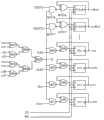
图1是显示了一个传统的与非(NAND)闪存设备中页复制备份特征的框图。FIG. 1 is a block diagram showing page copy backup features in a conventional NAND flash memory device.
图2是显示了根据本发明的实施例具有错误校正的页复制备份特征的框图。FIG. 2 is a block diagram illustrating a page copy backup feature with error correction according to an embodiment of the present invention.
图3是显示了根据本发明的实施例一个错误校正电路的框图。FIG. 3 is a block diagram showing an error correction circuit according to an embodiment of the present invention.
图4是显示了用于在页缓冲器和图3的错误校正电路之间执行数据传输的门电路的电路图。FIG. 4 is a circuit diagram showing gate circuits for performing data transfer between a page buffer and the error correction circuit of FIG. 3 .
图5是在页缓冲器和图3的错误校正电路之间数据传输的时序图。FIG. 5 is a timing diagram of data transfer between the page buffer and the error correction circuit of FIG. 3 .
图6是显示了根据本发明的实施例产生列和行校验位的程序的表格。Figure 6 is a table showing the procedure for generating column and row parity bits according to an embodiment of the present invention.
图7是显示了用于产生图6所示的列校验位的电路的电路图。FIG. 7 is a circuit diagram showing a circuit for generating the column parity bit shown in FIG. 6 .
图8是显示了用于产生图6所示的行校验位的电路的电路图。FIG. 8 is a circuit diagram showing a circuit for generating the row parity bit shown in FIG. 6 .
图9是在页缓冲器与错误校正电路之间的数据传输中使用的信号的时序图。FIG. 9 is a timing diagram of signals used in data transfer between the page buffer and the error correction circuit.
具体实施方式Detailed ways
将被理解的是优选实施例的描述仅仅是说明性的而并不是用于限定意义的。在下面的详细描述中,许多具体细节被说明用于提供对本发明更彻底的理解。然而,显而易见的是,即使没有这些具体细节对于本领域的技术人员而言本发明也是可以被实施的。It should be understood that the description of preferred embodiments is illustrative only and not in a limiting sense. In the following detailed description, numerous specific details are set forth in order to provide a more thorough understanding of the present invention. It will be apparent, however, that the present invention may be practiced by one skilled in the art without these specific details.
应用于本发明的闪存被体现在一NAND闪存上,适于嵌入在便携式电子设备中例如集成电路卡,其中许多的存储单元以串的模式被排列,这些串耦合到以行和列的矩阵布置的多个字线和位线。The flash memory applied to the present invention is embodied on a NAND flash memory, suitable for embedding in a portable electronic device such as an integrated circuit card, wherein a plurality of memory cells are arranged in a pattern of strings coupled to a matrix arranged in rows and columns multiple word lines and bit lines.
根据本发明的实施例NAND闪存具有一个被分为由地址指定的多个页的存储单元阵列。每一页由耦合到一个字线和一个个地耦合到多个位线的数个存储单元构成。该页是读和写的单位。A NAND flash memory according to an embodiment of the present invention has a memory cell array divided into a plurality of pages designated by addresses. Each page is made up of a number of memory cells coupled to a word line and individually coupled to bit lines. The page is the unit of reading and writing.
根据本发明的实施例NAND闪存被设计用于执行如下功能操作,例如擦除以删除存储在存储单元中的数据,编程以在存储单元中写数据,从存储器中读出数据(也就是,一个读出操作),在完成擦除和编程后验证以检查存储单元状态,以及页复制以不使用读出操作而将一页中的数据录制到另一页中。According to an embodiment of the present invention, NAND flash memory is designed to perform the following functional operations, such as erasing to delete data stored in memory cells, programming to write data in memory cells, and reading data from memory (that is, a read operation), verify after completion of erase and programming to check memory cell status, and page copy to record data from one page into another page without using read operation.
根据本发明的实施例NAND闪存包括一个用于暂时存储在编程,读出或页复制操作过程中要从存储单元读出的或从存储器外部下载的数据的页缓冲器电路。还包括用于选择具有从外部供给地址的页或存储单元的缓冲器和解码器,用于检测数据值的读出放大器,用于从/到存储单元阵列转移数据到/从输入/输出信道的门线路,和用于管理其中的操作的控制电路。The NAND flash memory according to the embodiment of the present invention includes a page buffer circuit for temporarily storing data to be read from memory cells or downloaded from outside the memory during programming, reading or page copying operations. Also included are buffers and decoders for selecting pages or memory cells with addresses supplied from the outside, sense amplifiers for detecting data values, transfer of data from/to memory cell arrays to/from input/output channels gate circuits, and control circuits for managing operations therein.
本发明的实施例包括一个与页复制功能结合的错误校正操作。Embodiments of the present invention include an error correction operation combined with a page copy function.
在该实施例中,术语“读出”用于指从存储器中读出数据的操作,也就是数据从存储器单元中移出存储器的状态。术语“复制”用于指转移特定页的数据到页缓冲器中的操作,以及“转录”用于指将保持在页缓冲器中的数据移动到另一个页中的操作。此外,“源数据”用于指具有错误位的被复制的数据,“修正(或纠正或改正)数据”用于指没有错误位的被转录的数据。In this embodiment, the term "read" is used to refer to the operation of reading data from the memory, that is, the state in which data is moved out of the memory cells from the memory cells. The term "copy" is used to refer to an operation of transferring data of a specific page into a page buffer, and "transcription" is used to refer to an operation of moving data held in a page buffer to another page. Also, "source data" is used to refer to copied data with erroneous bits, and "correction (or correction or correction) data" is used to refer to transcribed data without erroneous bits.
现在,结合图2至图9解释本发明的实用实施例。Now, a practical embodiment of the present invention is explained with reference to FIGS. 2 to 9 .
图2显示了根据本发明的实施例在页复制操作模式过程中校正一个位错误的示意特征。首先,存储在,例如,页PG4中的数据,即源数据,通过读操作(该读操作与用在当前说明中其他处的读出操作不同)被加载到页缓冲器10中,这被称为“复制”操作。存储在页缓冲器10中的该数据,也就是,页PG4的源数据(下文所指的“源页”)在它们被写入到另一页(例如,PGn-3;下文称为“转录页”)之前被输入到错误校正电路20来修正包含在源数据中的一个位错误。由错误校正电路20修改后的数据被转移回页缓冲器10中然后写入到页PGn-3中。结果,页PGn-3可以确保源数据中不包含错误位,防止通过源数据转录错误位。FIG. 2 shows schematic features of correcting a bit error during a page copy mode of operation according to an embodiment of the present invention. First, the data stored in, for example, page PG4, i.e. the source data, is loaded into the
即使将被转录的页PGn-4有自己的错误位,已知的错误校正功能可以修改其中单个的位错误。有关页复制操作过程中错误校正过程的细节将在下文中描述。Even if the page PGn-4 to be transcribed has its own erroneous bits, individual bit errors are corrected by known error correction functions. Details about the error correction process during the page copy operation will be described below.
图3显示了在页复制操作过程中用于处理错误校正的功能结构。参照图3,一旦暂时存储在页缓冲器10中的源数据De被提供给错误校正电路20时,比较器50比较旧校验位OP和在复制操作过程中由校验位产生器40产生的新校验位NP,该旧校验位是在先前的编程(或写)循环过程中被创建并且被存储在存储器的预定域中。该新校验位NP是用于校正一个位错误的校验数据,也就是在页复制操作过程中由源数据产生的一个累进位错误。该旧校验位和新校验位,OP和NP,通过相同的方式被产生。在比较了该旧校验位OP与该新校验位NP之后,涉及累进位错误的页地址的信息信号Ae由比较器50产生。该错误的地址信息信号Ae应用于一个错误校正逻辑电路60来修改该位错误。改正数据Dc与控制信号CNT一起从错误校正逻辑电路60转移到页缓冲器10。校验位产生和比较的细节将在下文进行描述。Figure 3 shows the functional structure for handling error correction during a page copy operation. Referring to FIG. 3, once the source data De temporarily stored in the
图4是锁存和列解码块LDB0~LDBm-1的电路图,该锁存和列解码块LDB0~LDBm-1被安排在页缓冲和读出(sensing)逻辑块12(包括在页缓冲器10中)与输入/输出线I/O0~I/On-1之间,用于转移源数据和校正数据。参照图4,分配到特定地址的源页(例如,PG4)的源数据通过每个都与输入/输出线I/O0~I/On-1相对应的锁存和列解码块LDB0~LDBm-1从页缓冲和读出块12转移到错误校正电路20。该锁存和列解码块LDB0~LDBm-1同样通过页缓冲和读出块12转移由错误校正电路20提供的改正数据Dc到转录页(例如,PGn-1)。Fig. 4 is the circuit diagram of latch and column decoding block LDB0~LDBm-1, and this latch and column decoding block LDB0~LDBm-1 are arranged in page buffer and read (sensing) logical block 12 (included in
源页PG4的源数据De通过页缓冲和检测块12读出并被存储到每个与位线BL0~BLn-1相对应的锁存器LCH0~LCHn-1中。响应于列门信号YA0~YAn-1(主要的)和YB0~YBk-1(次要的)暂留在存储器LCH0~LCHn-1中的源数据顺序地以位为单位通过列门(或Y-门)AG0~AGn-1和BG0~BGk-1转移到输入/输出线I/O0~I/On-1,如图5中所示,其可以被称作“错误数据输出”的操作状态。例如,当列门信号YA0和YB0都处于高电平有效时,与位线BL0相对应的源数据位通过输入/输出线I/O0被转移到错误校正电路20。The source data De of the source page PG4 is read through the page buffer and detection block 12 and stored in each of the latches LCH0 ˜ LCHn- 1 corresponding to the bit lines BL0 ˜BLn- 1 . In response to the column gate signals YA0~YAn-1 (primary) and YB0~YBk-1 (secondary), the source data remaining in the memory LCH0~LCHn-1 sequentially pass through the column gate (or Y -gates) AG0~AGn-1 and BG0~BGk-1 are transferred to the input/output lines I/O0~I/On-1, as shown in FIG. 5, which can be called the operation state of "error data output" . For example, when the column gate signals YA0 and YB0 are both active high, the source data bit corresponding to the bit line BL0 is transferred to the
改正数据Dc通过输入/输出线I/O0~I/On-1从错误校正电路20转移到每个都与位线BL0~BLn-1相连接的锁存器LCH0~LCHn-1,其可以被称为“改正数据的输入”的操作状态。例如,当列门信号YA0和YB0都处于高电平有效时,与位线BL0相对应的改正数据位通过输入/输出线I/O0转移到页缓冲器10(也就是,页缓冲和读出块12)。经由编程过程暂时存储在锁存器中的改正数据Dc被写入到转录页PGn-1中。The correction data Dc is transferred from the
图6显示了根据本发明的实施例产生新校验位NP的一个实用方式。先前存储在存储器预定域中的旧校验位OP是由一个在先的编程操作产生的。用于产生校验位的已知技术被简单划分为两种方式:一种是串行方式,另一种是并行方式。本发明的实施例使用该串行方式用以节省拓扑电路区域,但两种中的另一种实施方式也是可接受的。FIG. 6 shows a practical way to generate a new parity bit NP according to an embodiment of the present invention. The old parity bits OP previously stored in predetermined fields of the memory were generated by a previous programming operation. Known techniques for generating parity bits are simply divided into two ways: one is serial and the other is parallel. Embodiments of the present invention use this serial approach to save topological circuit area, but the other implementation of the two is also acceptable.
说明从中建立校验位的源数据De由8位的512字节组成,该校验位被分类为列校验位和行校验位。列校验位由一个字节的8位而获得,而行校验位由512字节获得。It is stated that the source data De from which the check digits are built consists of 512 bytes of 8 bits, which are classified into column check digits and row check digits. The column parity bit is obtained from 8 bits of a byte, and the row parity bit is obtained from 512 bytes.
列校验位和行校验位可以由图7和图8中分别所示的电路构成,两个电路都包括在图4所示的校验位产生器40中。列校验位和行校验位的产生是通过处理具有二进制组合的异或(XOR)逻辑链来完成的,用以从位或字节包中获得一个位错误。The column parity bit and the row parity bit can be constituted by the circuits shown in FIG. 7 and FIG. 8 respectively, and both circuits are included in the
现在参照图6和图7以b及下面的表1来描述关于从8位b0-b7创建列校验位的过程。Referring now to Figures 6 and 7 and b and Table 1 below, the process for creating a column parity bit from 8 bits b0-b7 is described.
[表1][Table 1]


字符“*”代表从相关位的结合获得比较结果的XOR运算符。因此,XOR逻辑完整的运算等式在下面被总结,每一个用于6位的列校验位。The character "*" represents the XOR operator that obtains the comparison result from the combination of the relevant bits. Therefore, the complete operational equations of the XOR logic are summarized below, each for a 6-bit column parity bit.
CP1=b7*b5*b3*b1CP1=b7*b5*b3*b1
nCP1=b6*b4*b2*b0nCP1=b6*b4*b2*b0
CP2=b7*b6*b3*b2CP2=b7*b6*b3*b2
nCP2=b5*b4*b1*b0nCP2=b5*b4*b1*b0
CP4=b7*b6*b5*b4CP4=b7*b6*b5*b4
nCP4=b3*b2*b1*b0nCP4=b3*b2*b1*b0
参照图7,为产生每个列校验位而执行的算法结合与4个XOR门XR和一个触发器FF相关。每个输入/输出线与每个数据位相对应。列校验位nCP4从接收XOR门XR19的输出的触发器FF6产生。门XR19接收XOR门XR13的输出和从触发器FF6反馈的列校验位nCP4。门XR13接收XOR门XR1和XR2的输出。输入/输出线I/O2和I/O3与门XR2的输入端连接,而输入/输出线I/O0和I/O1与门XR1的输入端连接。与nCP4互补的列校验位CP4是由接收XOR门XR20的输出的触发器FF5产生。门XR20接收XOR门XR14的输出和从触发器FF5反馈的列校验位CP4。门XR14接收XOR门XR3和XR4的输出。输入/输出线I/O4和I/O5与门XR3的输入端连接,而输入/输出线I/O6和I/O7与门XR4的输入端连接。Referring to FIG. 7, the algorithm performed for generating each column parity bit is associated with four XOR gates XR and one flip-flop FF. Each input/output line corresponds to each data bit. Column parity bit nCP4 is generated from flip-flop FF6 receiving the output of XOR gate XR19. The gate XR19 receives the output of the XOR gate XR13 and the column parity bit nCP4 fed back from the flip-flop FF6. Gate XR13 receives the outputs of XOR gates XR1 and XR2. Input/output lines I/O2 and I/O3 are connected to the input of gate XR2, and input/output lines I/O0 and I/O1 are connected to the input of gate XR1. The column parity bit CP4 complementary to nCP4 is generated by flip-flop FF5 receiving the output of XOR gate XR20. The gate XR20 receives the output of the XOR gate XR14 and the column parity bit CP4 fed back from the flip-flop FF5. Gate XR14 receives the outputs of XOR gates XR3 and XR4. Input/output lines I/O4 and I/O5 are connected to the input of gate XR3, and input/output lines I/O6 and I/O7 are connected to the input of gate XR4.
列校验位nCP2是由接收XOR门XR21的输出的触发器FF4产生。门XR21接收XOR门XR15的输出和从触发器FF4反馈的列校验位nCP2。门XR15接收XOR门XR5和XR6的输出。输入/输出线I/O0和I/O1与门XR5的输入端连接,而输入/输出线I/O4和I/O5与门XR6的输入端连接。与nCP2互补的列校验位CP2是由接收XOR门XR22的输出的触发器FF3产生。门XR22接收XOR门XR16的输出和从触发器FF3反馈的列校验位CP2。门XR16接收XOR门XR7和XR8的输出。输入/输出线I/O2和I/O3与门XR7的输入端连接,而输入/输出线I/O6和I/O7与门XR8的输入端连接。The column parity bit nCP2 is generated by the flip-flop FF4 receiving the output of the XOR gate XR21. The gate XR21 receives the output of the XOR gate XR15 and the column parity bit nCP2 fed back from the flip-flop FF4. Gate XR15 receives the outputs of XOR gates XR5 and XR6. Input/output lines I/O0 and I/O1 are connected to the input of gate XR5, and input/output lines I/O4 and I/O5 are connected to the input of gate XR6. Column parity bit CP2 complementary to nCP2 is generated by flip-flop FF3 receiving the output of XOR gate XR22. The gate XR22 receives the output of the XOR gate XR16 and the column parity bit CP2 fed back from the flip-flop FF3. Gate XR16 receives the outputs of XOR gates XR7 and XR8. Input/output lines I/O2 and I/O3 are connected to the input of gate XR7, while input/output lines I/O6 and I/O7 are connected to the input of gate XR8.
列校验位nCP1是由接收XOR门XR23的输出的触发器FF2产生。门XR23接收XOR门XR17的输出和从触发器FF2反馈的列校验位nCP1。门XR17接收XOR门XR9和XR10的输出。输入/输出线I/O0和I/O2与门XR9的输入端连接,而输入/输出线I/O4和I/O6与门XR10的输入端连接。与nCP2互补的列校验位CP1是由接收XOR门XR24的输出的触发器FF1产生。门XR24接收XOR门XR18的输出和从触发器FF1反馈的列校验位CP1。门XR18接收XOR门XR11和XR12的输出。输入/输出线I/O1和I/O3与门XR11的输入端连接,而输入/输出线I/O5和I/O7与门XR12的输入端连接。The column parity bit nCP1 is generated by the flip-flop FF2 receiving the output of the XOR gate XR23. The gate XR23 receives the output of the XOR gate XR17 and the column parity bit nCP1 fed back from the flip-flop FF2. Gate XR17 receives the outputs of XOR gates XR9 and XR10. Input/output lines I/O0 and I/O2 are connected to the input of gate XR9, while input/output lines I/O4 and I/O6 are connected to the input of gate XR10. Column parity bit CP1 complementary to nCP2 is generated by flip-flop FF1 receiving the output of XOR gate XR24. The gate XR24 receives the output of the XOR gate XR18 and the column parity bit CP1 fed back from the flip-flop FF1. Gate XR18 receives the outputs of XOR gates XR11 and XR12. The input/output lines I/O1 and I/O3 are connected to the input terminal of the gate XR11, and the input/output lines I/O5 and I/O7 are connected to the input terminal of the gate XR12.
时钟信号CLK和复位信号RST共同应用于触发器FF1~FF6。因此,触发器FF1~FF6响应于时钟信号CLK每个循环的上升沿输出列校验位。到位于其对应触发器之前的XOR门的每个列校验位的反馈输入(例如,NCP4从FF6到XR19)用于检测源数据中当前位和下一位之间的变化(也就是,检测在页复制操作过程中的累进位错误)然后采用产生校验位的串行方式来管理它。The clock signal CLK and the reset signal RST are jointly applied to the flip-flops FF1˜FF6. Therefore, the flip-flops FF1˜FF6 output column parity bits in response to the rising edge of each cycle of the clock signal CLK. The feedback input to each column parity bit of the XOR gate preceding its corresponding flip-flop (for example, NCP4 from FF6 to XR19) is used to detect changes between the current bit and the next bit in the source data (that is, to detect cumulative bit errors during page copy operations) and then manage it in a serial fashion that generates parity bits.
作为产生列校验位的一个实用的例子,列校验位CP1,CP2和nCP4被设置为“1”,假设位b3为一个错误位。As a practical example of generating column parity bits, column parity bits CP1, CP2 and nCP4 are set to "1", assuming that bit b3 is an error bit.
从512字节产生行校验位将参照图6和图8以及下面的表2进行描述。表2安排了用于XOR算法实现的字节结合以获得与源数据的512字节相对的行校验位LP1,nLP1,LP2,nLP2,LP4,nLP4…,LP512和nLP512(LP1~nLP512;18位)。Generation of row parity bits from 512 bytes will be described with reference to FIGS. 6 and 8 and Table 2 below. Table 2 arranges the combination of bytes used for XOR algorithm realization to obtain row parity bits LP1, nLP1, LP2, nLP2, LP4, nLP4..., LP512 and nLP512 (LP1~nLP512; 18 relative to 512 bytes of source data) bits).
[表2][Table 2]


在表2中,字符“*”表示由相应位的结合获得比较结果的XOR运算符,而“^B”表示用于它们相对应字节的8位的XOR操作的结果(例如,在第512字节个中^B512=b7*b6*b5*b4*b3*b2*b1*b0)。因子^B在下文中被称作“字节校验单元”。因此,表2中XOR逻辑的完整的运算等式在下面被总结,每一个用于18位的行校验位。In Table 2, the character "*" represents the XOR operator that obtains the comparison result by combining the corresponding bits, and "^B" represents the result of the XOR operation for the 8 bits of their corresponding bytes (for example, at 512 Among the bytes ^B512=b7*b6*b5*b4*b3*b2*b1*b0). The factor ^B is hereinafter referred to as a "Byte Check Unit". Therefore, the complete operational equations for the XOR logic in Table 2 are summarized below, each for an 18-bit row parity bit.
LP1=^B512*^B510*…*^B256*^B254*…*^B4*^B2LP1=^B512*^B510*…*^B256*^B254*…*^B4*^B2
nLP2=^B511*^B509*…*^B255*^B253*…*^B3*^B1nLP2=^B511*^B509*…*^B255*^B253*…*^B3*^B1
LP2=^B512*^B511*…*^B256*^B255*…*^B4*^B3LP2=^B512*^B511*…*^B256*^B255*…*^B4*^B3
nLP2=^B510*^B509*…*^B254*^B253*…*^B2*^B1nLP2=^B510*^B509*…*^B254*^B253*…*^B2*^B1
LP4=^B512*^B511*^B510*^B509*…*^B256*^B255*LP4=^B512*^B511*^B510*^B509*…*^B256*^B255*
^B254*^B253*…*^B8*^B7*^B6*^B5^B254*^B253*…*^B8*^B7*^B6*^B5
nLP4=^B508*^B507*^B506*^B505*…*^B252*^B251*nLP4=^B508*^B507*^B506*^B505*…*^B252*^B251*
^B250*^B249*…*^B4*^B3*^B2*^B1^B250*^B249*…*^B4*^B3*^B2*^B1
………………………………
LP512=^B512*^B511*^B510*^B509*…*^B260*^B259LP512=^B512*^B511*^B510*^B509*…*^B260*^B259
*^B258*^257*^B258*^257
nLP512=^B256*^B255*^B254*^B253*…*^B4*^B3nLP512=^B256*^B255*^B254*^B253*…*^B4*^B3
*^B2*^B1*^B2*^B1
参照图8,用于每个字节的字节校验单元^B通过XOR门XR31~XR37首先获得。字节校验单元^B由门XR37产生。门XR37接收门XR35和XR36的输出。门XR35接收门XR31和XR32的输出,而门XR36接收门XR33和XR34的输出。门XR31的输入端与输入/输出线I/O0和I/O1连接,而门XR32的输入端与输入/输出线I/O2和I/O3连接。门XR33的输入端与输入/输出线I/O4和I/O5连接,而门XR34的输入端与输入/输出线I/O6和I/O7连接。Referring to FIG. 8, the byte check unit ^B for each byte is first obtained through XOR gates XR31~XR37. The byte check unit ^B is produced by gate XR37. Gate XR37 receives the outputs of gates XR35 and XR36. Gate XR35 receives the outputs of gates XR31 and XR32, while gate XR36 receives the outputs of gates XR33 and XR34. The input terminal of the gate XR31 is connected to the input/output lines I/O0 and I/O1, and the input terminal of the gate XR32 is connected to the input/output lines I/O2 and I/O3. The input terminal of the gate XR33 is connected to the input/output lines I/O4 and I/O5, and the input terminal of the gate XR34 is connected to the input/output lines I/O6 and I/O7.
门XR37的输出,^B,分为18条路线用于产生18个行校验位LP1~nLP512,共同地施加到NAND门ND1~ND18的输入端。如果与它们对应字节的8位中有错误位,该字节校验单元^B被设置为“1”。NAND门ND1~ND18每一个响应时钟控制信号nCLK1,CLK1,nCLK2,CLK2,…,nCLK512和CLK512(nCLK1~CLK512;18ea)来控制从字节校验单元^B到行校验位的位路径。NAND门ND1~ND18的输出端与XOR门XR1~XR18的输入端分别连接。门XR1~XR18还分别接收从接收门XR1~XR18的输出的触发器FF1~FF18反馈到此的行校验位NLP1~LP18。The output of gate XR37, ^B, is divided into 18 routes for generating 18 row parity bits LP1~nLP512, which are commonly applied to the input terminals of NAND gates ND1~ND18. If there is an error bit in the 8 bits corresponding to them, the byte check unit ^B is set to "1". NAND gates ND1~ND18 each respond to clock control signals nCLK1, CLK1, nCLK2, CLK2, . The output ends of the NAND gates ND1-ND18 are respectively connected to the input ends of the XOR gates XR1-XR18. The gates XR1~XR18 also respectively receive the row parity bits NLP1~LP18 fed back here from the flip-flops FF1~FF18 receiving the outputs of the gates XR1~XR18.
由于时钟信号CLK和复位信号RST共同施加于触发器FF1~FF18,触发器FF1~FF18响应于时钟信号CLK每个周期的上升沿输出行校验位。到位于其对应触发器之前的XOR门的每个列校验位的反馈输入例如,LP512从FF1018到XR1018)用于检测源数据中当前位和下一位之间的变化(也就是,用于检测在页复制操作过程中的累进位错误)然后采用产生行校验位的串行方式来管理它。作为行校验位产生的实用的例子,如果字节B3有一个错误位,行校验位nLP1,LP2,nLP4,…,nLP512将被设置为“1”。Since the clock signal CLK and the reset signal RST are applied to the flip-flops FF1-FF18, the flip-flops FF1-FF18 output the row parity bit in response to the rising edge of each cycle of the clock signal CLK. The feedback input to each column parity bit of the XOR gate preceding its corresponding flip-flop (for example, LP512 from FF1018 to XR1018) is used to detect the change between the current bit and the next bit in the source data (that is, for detects progressive bit errors during page copy operations) and manages it in a serial fashion by generating row parity bits. As a practical example of row parity generation, if byte B3 has an error bit, row parity bits nLP1, LP2, nLP4, . . . , nLP512 will be set to "1".
图9的时序图显示了用于从页缓冲器10到错误校正电路20转移源数据的列门信号和时钟控制信号的脉冲状态,与图4至图8中电路的操作相结合。图9中所示的传输过程示例性地通过图4中所示的锁存和列解码块LDB1执行。The timing diagram of FIG. 9 shows pulse states of column gate signals and clock control signals for transferring source data from
参照图9,由于对于次要的列门信号YB0处于高电平使能状态主要的列门信号YA0~YAn-1连续的处于高电平有效状态,与位线BL0~BLn-1相对应的数据位通过其对应的输入/输出线I/O0~I/On-1被顺序地转移到错误校正电路20。通过相同的方式,根据对于次要的列门信号YB0~YBk-1的每一个有效状态的主要的列门信号YA0~YAn-1的顺序有效状态,源数据的所有512字节通过输入/输出线I/O0~I/ON-1被转移到错误校正电路20。Referring to FIG. 9, since the main column gate signals YA0~YAn-1 are continuously in the high-level active state for the secondary column gate signal YB0 in the high-level enable state, the corresponding bit lines BL0~BLn-1 The data bits are sequentially transferred to the
在错误校正电路20中,响应于时钟信号CLK的周期振荡,图7中所示的列校验位产生器的触发器FF1~FF6输出列校验位CP1~nCP4。同时,从时钟信号CLK分离出来的的时钟控制信号CLK1~nCLK512使位路径能够通过图8中所示的行校验位产生器的NAND门ND1~ND18传导,而行校验位产生器的触发器FF1~FF18输出18位的行校验位LP1~nLP512。In the
新校验位NP的位数是24,它是由8个列校验位CP1~nCP4和18个行校验位LP1~nLP512组成的,它与存储在闪存的预定域中的旧校验位OP相同。用于执行具有错误校正的页复制操作的完整的顺序如下所述。The number of digits of the new parity bit NP is 24, which is composed of 8 column parity bits CP1~nCP4 and 18 row parity bits LP1~nLP512, which are stored in the predetermined field of the flash memory. OP is the same. The complete sequence for performing a page copy operation with error correction is as follows.
首先,在编程期间产生旧校验位OP并存储在存储器的预定域中。然后,如图6至图8中所示的电路和上述的步骤产生新校验位NP。旧校验位和新校验位通过24位相互比较。First, the old parity bit OP is generated during programming and stored in a predetermined field of the memory. Then, the circuits shown in FIGS. 6 to 8 and the above steps generate a new parity bit NP. The old check digit and the new check digit are compared with each other by 24 bits.
在通过校验位比较器50比较旧校验位OP与新校验位NP的过程中,如果旧校验位和新校验位的所有24位相同(也就是,旧校验位与新校验位XOR操作的结果为“0”),则认为没有错误位。另一方面,当旧校验位和新校验位之间12位(24位的一半)的比较结果为“1”时,认为有一位错误。该一位的错误由校正逻辑电路60来修改。另外,只有当24位中的一位的比较结果为“1”时,才认为是在该页被复制时源数据中已经包含的一个单独的错误。除了上述情况,其他情况的比较结果可以认为有多于两位的错误位。In the process of comparing the old parity bit OP with the new parity bit NP by the
这样的位错误情况可以通过用户响应于一个命令而得以识别。进一步,它可以执行转录改正数据到源页和转录页。Such bit error conditions can be identified by the user in response to a command. Further, it can perform transcribing correction data to the source page and transcribing the page.
根据本发明的实施例,错误校正电路可以嵌入在闪存中。According to an embodiment of the present invention, error correction circuits may be embedded in flash memory.
如上所述,由于源页的源数据中包含的错误位在被写入到转录页之前由错误校正电路检测并修改,它可以防止源数据中的错误位被录制到转录页中。As described above, since the error bits contained in the source data of the source page are detected and corrected by the error correction circuit before being written into the transcription page, it can prevent the error bits in the source data from being recorded into the transcription page.
此外,根据本发明的闪存有效的消除了在页复制操作过程中产生的一个累进位错误。In addition, the flash memory according to the present invention effectively eliminates a progressive bit error generated during the page copy operation.
并且,根据上述的实施例,在页复制操作过程中不需要用于校正错误的缓冲部件,因为基本上在普通闪存中采用的页缓冲器,可有效地用于协助操作而不需要额外的修改。Also, according to the above-described embodiments, a buffer unit for correcting errors is not required during a page copy operation, because the page buffer basically employed in a general flash memory can be effectively used to assist the operation without additional modification .
虽然本发明的优选实施例被公开以用于说明目的,本领域的技术人员将认识到,在不脱离本发明所附权利要求中所描述的精神和范围下,各种修改,增加和替代都是可能的。Although the preferred embodiment of the present invention has been disclosed for illustrative purposes, those skilled in the art will recognize that various modifications, additions and substitutions can be made without departing from the spirit and scope of the present invention as described in the appended claims. It is possible.
本申请要求申请日为2003年4月3日的韩国专利申请NO.2003-21114的优先权,其全部内容在这里结合作为参考。This application claims priority from Korean Patent Application No. 2003-21114 filed on Apr. 3, 2003, the entire contents of which are incorporated herein by reference.
Claims (14)
Translated fromChineseApplications Claiming Priority (3)
| Application Number | Priority Date | Filing Date | Title |
|---|---|---|---|
| KR21114/03 | 2003-04-03 | ||
| KR1020030021114AKR100543447B1 (en) | 2003-04-03 | 2003-04-03 | Flash memory device with error correction |
| CN2004100477591ACN1551244B (en) | 2003-04-03 | 2004-04-05 | Error correctable nonvolatile memory for page copy operation and method thereof |
Related Parent Applications (1)
| Application Number | Title | Priority Date | Filing Date |
|---|---|---|---|
| CN2004100477591ADivisionCN1551244B (en) | 2003-04-03 | 2004-04-05 | Error correctable nonvolatile memory for page copy operation and method thereof |
Publications (2)
| Publication Number | Publication Date |
|---|---|
| CN103136068Atrue CN103136068A (en) | 2013-06-05 |
| CN103136068B CN103136068B (en) | 2017-05-31 |
Family
ID=32844907
Family Applications (3)
| Application Number | Title | Priority Date | Filing Date |
|---|---|---|---|
| CN2011100089100APendingCN102034545A (en) | 2003-04-03 | 2004-04-05 | Nonvolatile memory with page copy capability and method thereof |
| CN201310047282.6AExpired - LifetimeCN103136068B (en) | 2003-04-03 | 2004-04-05 | For page replicate operation can error correction nonvolatile memory and its method |
| CN2004100477591AExpired - LifetimeCN1551244B (en) | 2003-04-03 | 2004-04-05 | Error correctable nonvolatile memory for page copy operation and method thereof |
Family Applications Before (1)
| Application Number | Title | Priority Date | Filing Date |
|---|---|---|---|
| CN2011100089100APendingCN102034545A (en) | 2003-04-03 | 2004-04-05 | Nonvolatile memory with page copy capability and method thereof |
Family Applications After (1)
| Application Number | Title | Priority Date | Filing Date |
|---|---|---|---|
| CN2004100477591AExpired - LifetimeCN1551244B (en) | 2003-04-03 | 2004-04-05 | Error correctable nonvolatile memory for page copy operation and method thereof |
Country Status (6)
| Country | Link |
|---|---|
| US (3) | US7296128B2 (en) |
| EP (1) | EP1465203B1 (en) |
| JP (1) | JP2004311010A (en) |
| KR (1) | KR100543447B1 (en) |
| CN (3) | CN102034545A (en) |
| DE (1) | DE602004003275T2 (en) |
Cited By (2)
| Publication number | Priority date | Publication date | Assignee | Title |
|---|---|---|---|---|
| CN106775454A (en)* | 2016-11-21 | 2017-05-31 | 建荣半导体(深圳)有限公司 | A kind of method and its device for managing bad column address |
| CN107203435A (en)* | 2016-03-17 | 2017-09-26 | 三星电子株式会社 | The operating method of non-volatile memory devices and the non-volatile memory devices |
Families Citing this family (129)
| Publication number | Priority date | Publication date | Assignee | Title |
|---|---|---|---|---|
| US7881133B2 (en)* | 2003-11-11 | 2011-02-01 | Samsung Electronics Co., Ltd. | Method of managing a flash memory and the flash memory |
| JP4237648B2 (en)* | 2004-01-30 | 2009-03-11 | 株式会社東芝 | Nonvolatile semiconductor memory device |
| US7466597B2 (en)* | 2004-09-09 | 2008-12-16 | Samsung Electronics Co., Ltd. | NAND flash memory device and copyback program method for same |
| US7849381B2 (en)* | 2004-12-21 | 2010-12-07 | Sandisk Corporation | Method for copying data in reprogrammable non-volatile memory |
| US7379368B2 (en)* | 2005-02-25 | 2008-05-27 | Frankfurt Gmbh, Llc | Method and system for reducing volatile DRAM power budget |
| KR100626393B1 (en) | 2005-04-07 | 2006-09-20 | 삼성전자주식회사 | Nonvolatile Memory Device and Its Multi-Page Copyback Method |
| KR100669352B1 (en)* | 2005-09-07 | 2007-01-16 | 삼성전자주식회사 | NAND flash memory device capable of performing error detection and data reloading operations during copy back program operation |
| KR101197556B1 (en)* | 2006-01-09 | 2012-11-09 | 삼성전자주식회사 | Device and method capable of verifying program operation of non-volatile memory and memory card including the same |
| EP1808863A1 (en)* | 2006-01-16 | 2007-07-18 | Deutsche Thomson-Brandt Gmbh | Method and apparatus for recording high-speed input data into a matrix of memory devices |
| JP4956230B2 (en)* | 2006-04-10 | 2012-06-20 | 株式会社東芝 | Memory controller |
| JP4908083B2 (en)* | 2006-06-30 | 2012-04-04 | 株式会社東芝 | Memory controller |
| JP5378664B2 (en)* | 2006-08-28 | 2013-12-25 | 三星電子株式会社 | Flash memory device having multi-page copyback function and block replacement method thereof |
| KR100755718B1 (en) | 2006-09-04 | 2007-09-05 | 삼성전자주식회사 | Apparatus and method for managing run-time bad blocks in multi-level cell flash memory |
| JP2008077810A (en)* | 2006-09-25 | 2008-04-03 | Toshiba Corp | Nonvolatile semiconductor memory device |
| JP4655034B2 (en)* | 2006-12-25 | 2011-03-23 | Tdk株式会社 | Memory controller, flash memory system, and flash memory control method |
| KR100882841B1 (en)* | 2007-06-19 | 2009-02-10 | 삼성전자주식회사 | Memory system capable of detecting bit error due to read disturbance and its reading method |
| KR100898673B1 (en) | 2007-08-08 | 2009-05-22 | 주식회사 하이닉스반도체 | Flash memory device and its operation method |
| US8055852B2 (en) | 2007-08-15 | 2011-11-08 | Micron Technology, Inc. | Memory device and method having on-board processing logic for facilitating interface with multiple processors, and computer system using same |
| US8291174B2 (en) | 2007-08-15 | 2012-10-16 | Micron Technology, Inc. | Memory device and method having on-board address protection system for facilitating interface with multiple processors, and computer system using same |
| US7822911B2 (en)* | 2007-08-15 | 2010-10-26 | Micron Technology, Inc. | Memory device and method with on-board cache system for facilitating interface with multiple processors, and computer system using same |
| KR101425957B1 (en)* | 2007-08-21 | 2014-08-06 | 삼성전자주식회사 | Ecc control circuit and multi channel memory system icluding the same |
| US9582417B2 (en)* | 2007-08-30 | 2017-02-28 | Virident Systems, Llc | Memory apparatus and methods thereof for preventing read errors on weak pages in a non-volatile memory system |
| US8443260B2 (en)* | 2007-12-27 | 2013-05-14 | Sandisk Il Ltd. | Error correction in copy back memory operations |
| US8762620B2 (en) | 2007-12-27 | 2014-06-24 | Sandisk Enterprise Ip Llc | Multiprocessor storage controller |
| US9594679B2 (en) | 2008-05-01 | 2017-03-14 | Sandisk Il Ltd. | Flash cache flushing method and system |
| JP2010009141A (en) | 2008-06-24 | 2010-01-14 | Toshiba Corp | Data transfer method |
| CN101615420B (en)* | 2008-06-26 | 2014-01-08 | 威刚科技股份有限公司 | Flash memory storage device with data correction function |
| TWI382422B (en)* | 2008-07-11 | 2013-01-11 | Genesys Logic Inc | Storage device for refreshing data pages of flash memory based on error correction code and method for the same |
| KR101030146B1 (en)* | 2008-08-29 | 2011-04-18 | 서울대학교산학협력단 | Flash-based storage using page buffer as write cache and method of use |
| US8433845B2 (en) | 2009-04-08 | 2013-04-30 | Google Inc. | Data storage device which serializes memory device ready/busy signals |
| US8205037B2 (en)* | 2009-04-08 | 2012-06-19 | Google Inc. | Data storage device capable of recognizing and controlling multiple types of memory chips operating at different voltages |
| CN102576330B (en)* | 2009-06-12 | 2015-01-28 | 提琴存储器公司 | Storage system with persistent garbage collection mechanism |
| US8214700B2 (en)* | 2009-10-28 | 2012-07-03 | Sandisk Technologies Inc. | Non-volatile memory and method with post-write read and adaptive re-write to manage errors |
| CN101699406B (en)* | 2009-11-12 | 2011-12-14 | 威盛电子股份有限公司 | Data storage system and method |
| TWI417887B (en)* | 2009-12-02 | 2013-12-01 | Via Tech Inc | Data storage system and method |
| CN102117230B (en)* | 2009-12-31 | 2013-01-09 | 群联电子股份有限公司 | Data writing method, flash memory controller and flash memory storage device |
| US8365041B2 (en) | 2010-03-17 | 2013-01-29 | Sandisk Enterprise Ip Llc | MLC self-raid flash data protection scheme |
| US10026458B2 (en) | 2010-10-21 | 2018-07-17 | Micron Technology, Inc. | Memories and methods for performing vector atomic memory operations with mask control and variable data length and data unit size |
| US20120110244A1 (en)* | 2010-11-02 | 2012-05-03 | Micron Technology, Inc. | Copyback operations |
| JP2012133843A (en)* | 2010-12-21 | 2012-07-12 | Toshiba Corp | Semiconductor storage device |
| US8560922B2 (en) | 2011-03-04 | 2013-10-15 | International Business Machines Corporation | Bad block management for flash memory |
| US8589775B2 (en)* | 2011-03-14 | 2013-11-19 | Infineon Technologies Ag | Error tolerant flip-flops |
| US20120324156A1 (en)* | 2011-06-17 | 2012-12-20 | Naveen Muralimanohar | Method and system of organizing a heterogeneous memory architecture |
| US8909982B2 (en) | 2011-06-19 | 2014-12-09 | Sandisk Enterprise Ip Llc | System and method for detecting copyback programming problems |
| US8910020B2 (en) | 2011-06-19 | 2014-12-09 | Sandisk Enterprise Ip Llc | Intelligent bit recovery for flash memory |
| US9158621B2 (en) | 2011-08-29 | 2015-10-13 | Sandisk Technologies Inc. | System and method of copying data |
| US8938658B2 (en) | 2011-11-07 | 2015-01-20 | Sandisk Enterprise Ip Llc | Statistical read comparison signal generation for memory systems |
| US8924815B2 (en) | 2011-11-18 | 2014-12-30 | Sandisk Enterprise Ip Llc | Systems, methods and devices for decoding codewords having multiple parity segments |
| US8954822B2 (en) | 2011-11-18 | 2015-02-10 | Sandisk Enterprise Ip Llc | Data encoder and decoder using memory-specific parity-check matrix |
| US9048876B2 (en) | 2011-11-18 | 2015-06-02 | Sandisk Enterprise Ip Llc | Systems, methods and devices for multi-tiered error correction |
| US9223649B2 (en)* | 2012-02-15 | 2015-12-29 | Sandisk Technologies Inc. | System and method of sending correction data to a buffer of a non-volatile memory |
| US8625386B2 (en)* | 2012-03-22 | 2014-01-07 | Seiko Epson Corporation | Non-volatile memory device, circuit board, printing material container and printer |
| US9699263B1 (en) | 2012-08-17 | 2017-07-04 | Sandisk Technologies Llc. | Automatic read and write acceleration of data accessed by virtual machines |
| US8996951B2 (en) | 2012-11-15 | 2015-03-31 | Elwha, Llc | Error correction with non-volatile memory on an integrated circuit |
| US9501398B2 (en) | 2012-12-26 | 2016-11-22 | Sandisk Technologies Llc | Persistent storage device with NVRAM for staging writes |
| US9612948B2 (en) | 2012-12-27 | 2017-04-04 | Sandisk Technologies Llc | Reads and writes between a contiguous data block and noncontiguous sets of logical address blocks in a persistent storage device |
| US9239751B1 (en) | 2012-12-27 | 2016-01-19 | Sandisk Enterprise Ip Llc | Compressing data from multiple reads for error control management in memory systems |
| US9003264B1 (en) | 2012-12-31 | 2015-04-07 | Sandisk Enterprise Ip Llc | Systems, methods, and devices for multi-dimensional flash RAID data protection |
| US9454420B1 (en) | 2012-12-31 | 2016-09-27 | Sandisk Technologies Llc | Method and system of reading threshold voltage equalization |
| US9214965B2 (en) | 2013-02-20 | 2015-12-15 | Sandisk Enterprise Ip Llc | Method and system for improving data integrity in non-volatile storage |
| US9329928B2 (en) | 2013-02-20 | 2016-05-03 | Sandisk Enterprise IP LLC. | Bandwidth optimization in a non-volatile memory system |
| US9870830B1 (en) | 2013-03-14 | 2018-01-16 | Sandisk Technologies Llc | Optimal multilevel sensing for reading data from a storage medium |
| US9009576B1 (en) | 2013-03-15 | 2015-04-14 | Sandisk Enterprise Ip Llc | Adaptive LLR based on syndrome weight |
| US9236886B1 (en) | 2013-03-15 | 2016-01-12 | Sandisk Enterprise Ip Llc | Universal and reconfigurable QC-LDPC encoder |
| US9367246B2 (en) | 2013-03-15 | 2016-06-14 | Sandisk Technologies Inc. | Performance optimization of data transfer for soft information generation |
| US9136877B1 (en) | 2013-03-15 | 2015-09-15 | Sandisk Enterprise Ip Llc | Syndrome layered decoding for LDPC codes |
| US9244763B1 (en) | 2013-03-15 | 2016-01-26 | Sandisk Enterprise Ip Llc | System and method for updating a reading threshold voltage based on symbol transition information |
| US9092350B1 (en) | 2013-03-15 | 2015-07-28 | Sandisk Enterprise Ip Llc | Detection and handling of unbalanced errors in interleaved codewords |
| US9170941B2 (en) | 2013-04-05 | 2015-10-27 | Sandisk Enterprises IP LLC | Data hardening in a storage system |
| US10049037B2 (en) | 2013-04-05 | 2018-08-14 | Sandisk Enterprise Ip Llc | Data management in a storage system |
| US9159437B2 (en) | 2013-06-11 | 2015-10-13 | Sandisk Enterprise IP LLC. | Device and method for resolving an LM flag issue |
| US9384126B1 (en) | 2013-07-25 | 2016-07-05 | Sandisk Technologies Inc. | Methods and systems to avoid false negative results in bloom filters implemented in non-volatile data storage systems |
| US9524235B1 (en) | 2013-07-25 | 2016-12-20 | Sandisk Technologies Llc | Local hash value generation in non-volatile data storage systems |
| US9043517B1 (en) | 2013-07-25 | 2015-05-26 | Sandisk Enterprise Ip Llc | Multipass programming in buffers implemented in non-volatile data storage systems |
| US9639463B1 (en) | 2013-08-26 | 2017-05-02 | Sandisk Technologies Llc | Heuristic aware garbage collection scheme in storage systems |
| US9361221B1 (en) | 2013-08-26 | 2016-06-07 | Sandisk Technologies Inc. | Write amplification reduction through reliable writes during garbage collection |
| US9442670B2 (en) | 2013-09-03 | 2016-09-13 | Sandisk Technologies Llc | Method and system for rebalancing data stored in flash memory devices |
| US9519577B2 (en) | 2013-09-03 | 2016-12-13 | Sandisk Technologies Llc | Method and system for migrating data between flash memory devices |
| US9158349B2 (en) | 2013-10-04 | 2015-10-13 | Sandisk Enterprise Ip Llc | System and method for heat dissipation |
| US9323637B2 (en) | 2013-10-07 | 2016-04-26 | Sandisk Enterprise Ip Llc | Power sequencing and data hardening architecture |
| US9442662B2 (en) | 2013-10-18 | 2016-09-13 | Sandisk Technologies Llc | Device and method for managing die groups |
| US9298608B2 (en) | 2013-10-18 | 2016-03-29 | Sandisk Enterprise Ip Llc | Biasing for wear leveling in storage systems |
| US9436831B2 (en) | 2013-10-30 | 2016-09-06 | Sandisk Technologies Llc | Secure erase in a memory device |
| US9263156B2 (en) | 2013-11-07 | 2016-02-16 | Sandisk Enterprise Ip Llc | System and method for adjusting trip points within a storage device |
| US9244785B2 (en) | 2013-11-13 | 2016-01-26 | Sandisk Enterprise Ip Llc | Simulated power failure and data hardening |
| US9152555B2 (en) | 2013-11-15 | 2015-10-06 | Sandisk Enterprise IP LLC. | Data management with modular erase in a data storage system |
| US9703816B2 (en) | 2013-11-19 | 2017-07-11 | Sandisk Technologies Llc | Method and system for forward reference logging in a persistent datastore |
| US9520197B2 (en) | 2013-11-22 | 2016-12-13 | Sandisk Technologies Llc | Adaptive erase of a storage device |
| US9280429B2 (en) | 2013-11-27 | 2016-03-08 | Sandisk Enterprise Ip Llc | Power fail latching based on monitoring multiple power supply voltages in a storage device |
| US9122636B2 (en) | 2013-11-27 | 2015-09-01 | Sandisk Enterprise Ip Llc | Hard power fail architecture |
| US9520162B2 (en) | 2013-11-27 | 2016-12-13 | Sandisk Technologies Llc | DIMM device controller supervisor |
| US9250676B2 (en) | 2013-11-29 | 2016-02-02 | Sandisk Enterprise Ip Llc | Power failure architecture and verification |
| US9582058B2 (en) | 2013-11-29 | 2017-02-28 | Sandisk Technologies Llc | Power inrush management of storage devices |
| US9092370B2 (en) | 2013-12-03 | 2015-07-28 | Sandisk Enterprise Ip Llc | Power failure tolerant cryptographic erase |
| US9235245B2 (en) | 2013-12-04 | 2016-01-12 | Sandisk Enterprise Ip Llc | Startup performance and power isolation |
| US9129665B2 (en) | 2013-12-17 | 2015-09-08 | Sandisk Enterprise Ip Llc | Dynamic brownout adjustment in a storage device |
| US9549457B2 (en) | 2014-02-12 | 2017-01-17 | Sandisk Technologies Llc | System and method for redirecting airflow across an electronic assembly |
| US9497889B2 (en) | 2014-02-27 | 2016-11-15 | Sandisk Technologies Llc | Heat dissipation for substrate assemblies |
| US9703636B2 (en) | 2014-03-01 | 2017-07-11 | Sandisk Technologies Llc | Firmware reversion trigger and control |
| US9348377B2 (en) | 2014-03-14 | 2016-05-24 | Sandisk Enterprise Ip Llc | Thermal isolation techniques |
| US9519319B2 (en) | 2014-03-14 | 2016-12-13 | Sandisk Technologies Llc | Self-supporting thermal tube structure for electronic assemblies |
| US9485851B2 (en) | 2014-03-14 | 2016-11-01 | Sandisk Technologies Llc | Thermal tube assembly structures |
| US9448876B2 (en) | 2014-03-19 | 2016-09-20 | Sandisk Technologies Llc | Fault detection and prediction in storage devices |
| US9390814B2 (en) | 2014-03-19 | 2016-07-12 | Sandisk Technologies Llc | Fault detection and prediction for data storage elements |
| US9454448B2 (en) | 2014-03-19 | 2016-09-27 | Sandisk Technologies Llc | Fault testing in storage devices |
| US9626399B2 (en) | 2014-03-31 | 2017-04-18 | Sandisk Technologies Llc | Conditional updates for reducing frequency of data modification operations |
| US9626400B2 (en) | 2014-03-31 | 2017-04-18 | Sandisk Technologies Llc | Compaction of information in tiered data structure |
| US9390021B2 (en) | 2014-03-31 | 2016-07-12 | Sandisk Technologies Llc | Efficient cache utilization in a tiered data structure |
| US9697267B2 (en) | 2014-04-03 | 2017-07-04 | Sandisk Technologies Llc | Methods and systems for performing efficient snapshots in tiered data structures |
| US10656842B2 (en) | 2014-05-30 | 2020-05-19 | Sandisk Technologies Llc | Using history of I/O sizes and I/O sequences to trigger coalesced writes in a non-volatile storage device |
| US9093160B1 (en) | 2014-05-30 | 2015-07-28 | Sandisk Technologies Inc. | Methods and systems for staggered memory operations |
| US10372613B2 (en) | 2014-05-30 | 2019-08-06 | Sandisk Technologies Llc | Using sub-region I/O history to cache repeatedly accessed sub-regions in a non-volatile storage device |
| US10114557B2 (en) | 2014-05-30 | 2018-10-30 | Sandisk Technologies Llc | Identification of hot regions to enhance performance and endurance of a non-volatile storage device |
| US10146448B2 (en) | 2014-05-30 | 2018-12-04 | Sandisk Technologies Llc | Using history of I/O sequences to trigger cached read ahead in a non-volatile storage device |
| US9703491B2 (en) | 2014-05-30 | 2017-07-11 | Sandisk Technologies Llc | Using history of unaligned writes to cache data and avoid read-modify-writes in a non-volatile storage device |
| US10656840B2 (en) | 2014-05-30 | 2020-05-19 | Sandisk Technologies Llc | Real-time I/O pattern recognition to enhance performance and endurance of a storage device |
| US8891303B1 (en) | 2014-05-30 | 2014-11-18 | Sandisk Technologies Inc. | Method and system for dynamic word line based configuration of a three-dimensional memory device |
| US10162748B2 (en) | 2014-05-30 | 2018-12-25 | Sandisk Technologies Llc | Prioritizing garbage collection and block allocation based on I/O history for logical address regions |
| US9070481B1 (en) | 2014-05-30 | 2015-06-30 | Sandisk Technologies Inc. | Internal current measurement for age measurements |
| US9645749B2 (en) | 2014-05-30 | 2017-05-09 | Sandisk Technologies Llc | Method and system for recharacterizing the storage density of a memory device or a portion thereof |
| US9652381B2 (en) | 2014-06-19 | 2017-05-16 | Sandisk Technologies Llc | Sub-block garbage collection |
| US9443601B2 (en) | 2014-09-08 | 2016-09-13 | Sandisk Technologies Llc | Holdup capacitor energy harvesting |
| US9478314B2 (en)* | 2014-09-15 | 2016-10-25 | Macronix International Co., Ltd. | Memory utilizing bundle-level status values and bundle status circuits |
| KR102248207B1 (en) | 2014-10-30 | 2021-05-06 | 삼성전자주식회사 | Storage device and operating method thereof |
| KR102023121B1 (en)* | 2014-10-31 | 2019-11-04 | 에스케이하이닉스 주식회사 | Memory device which corrects error and method of correcting error |
| KR102336458B1 (en)* | 2015-07-30 | 2021-12-08 | 삼성전자주식회사 | Non-volatile memory device and test system therof |
| US9619321B1 (en)* | 2015-10-08 | 2017-04-11 | Seagate Technology Llc | Internal copy-back with read-verify |
| US10853170B2 (en)* | 2018-09-06 | 2020-12-01 | Texas Instruments Incorporated | ECC protected storage |
| US12436689B1 (en) | 2024-07-02 | 2025-10-07 | Macronix International Co., Ltd. | Memory device and detection method for defeated status of memory cell |
Citations (2)
| Publication number | Priority date | Publication date | Assignee | Title |
|---|---|---|---|---|
| US6266273B1 (en)* | 2000-08-21 | 2001-07-24 | Sandisk Corporation | Method and structure for reliable data copy operation for non-volatile memories |
| US6339546B1 (en)* | 1999-09-17 | 2002-01-15 | Hitachi, Ltd. | Storage device counting error correction |
Family Cites Families (30)
| Publication number | Priority date | Publication date | Assignee | Title |
|---|---|---|---|---|
| JPS52129334A (en)* | 1976-04-23 | 1977-10-29 | Nec Corp | Memor |
| US4358848A (en)* | 1980-11-14 | 1982-11-09 | International Business Machines Corporation | Dual function ECC system with block check byte |
| US4453251A (en)* | 1981-10-13 | 1984-06-05 | Burroughs Corporation | Error-correcting memory with low storage overhead and fast correction mechanism |
| JPH05128882A (en)* | 1991-11-06 | 1993-05-25 | Mitsubishi Electric Corp | Data processing device |
| JPH05174496A (en)* | 1991-12-25 | 1993-07-13 | Sony Corp | Id signal processor for digital recorder |
| KR950003013B1 (en)* | 1992-03-30 | 1995-03-29 | 삼성전자 주식회사 | Eeprom with error correcting circuit |
| US5657332A (en)* | 1992-05-20 | 1997-08-12 | Sandisk Corporation | Soft errors handling in EEPROM devices |
| US5532962A (en)* | 1992-05-20 | 1996-07-02 | Sandisk Corporation | Soft errors handling in EEPROM devices |
| US5343426A (en)* | 1992-06-11 | 1994-08-30 | Digital Equipment Corporation | Data formater/converter for use with solid-state disk memory using storage devices with defects |
| US5459742A (en)* | 1992-06-11 | 1995-10-17 | Quantum Corporation | Solid state disk memory using storage devices with defects |
| US5754753A (en)* | 1992-06-11 | 1998-05-19 | Digital Equipment Corporation | Multiple-bit error correction in computer main memory |
| JPH08153045A (en)* | 1994-11-30 | 1996-06-11 | Nec Corp | Memory control circuit |
| US5838614A (en)* | 1995-07-31 | 1998-11-17 | Lexar Microsystems, Inc. | Identification and verification of a sector within a block of mass storage flash memory |
| KR0172366B1 (en)* | 1995-11-10 | 1999-03-30 | 김광호 | Read and program method of nonvolatile semiconductor memory device and circuit thereof |
| DE69716233T2 (en)* | 1996-08-16 | 2003-02-20 | Tokyo Electron Device Ltd., Yokohama | SEMICONDUCTOR MEMORY ARRANGEMENT WITH ERROR DETECTION AND CORRECTION |
| US5978952A (en)* | 1996-12-31 | 1999-11-02 | Intel Corporation | Time-distributed ECC scrubbing to correct memory errors |
| JPH10302485A (en)* | 1997-04-28 | 1998-11-13 | Hitachi Inf Technol:Kk | Information processing device having flash memory |
| JPH10340575A (en)* | 1997-06-04 | 1998-12-22 | Sony Corp | External memory device, its controller and data transmission/reception device |
| JP3173438B2 (en)* | 1997-06-04 | 2001-06-04 | ソニー株式会社 | Memory card and mounting device |
| US6040997A (en)* | 1998-03-25 | 2000-03-21 | Lexar Media, Inc. | Flash memory leveling architecture having no external latch |
| JP2001006379A (en)* | 1999-06-16 | 2001-01-12 | Fujitsu Ltd | Flash memory with copy and move functions |
| JP4165990B2 (en)* | 1999-12-20 | 2008-10-15 | Tdk株式会社 | MEMORY CONTROLLER, FLASH MEMORY SYSTEM PROVIDED WITH MEMORY CONTROLLER, AND METHOD FOR WRITEING DATA TO FLASH MEMORY |
| US6728913B1 (en)* | 2000-02-25 | 2004-04-27 | Advanced Micro Devices, Inc. | Data recycling in memory |
| US7356752B2 (en)* | 2000-03-14 | 2008-04-08 | Comtech Telecommunications Corp. | Enhanced turbo product codes |
| US6941505B2 (en)* | 2000-09-12 | 2005-09-06 | Hitachi, Ltd. | Data processing system and data processing method |
| JP2002351685A (en)* | 2001-05-22 | 2002-12-06 | Sankyo Seiki Mfg Co Ltd | Data updating method and controller for nonvolatile memory |
| JP2003030993A (en)* | 2001-07-17 | 2003-01-31 | Toshiba Corp | Semiconductor storage device |
| US6775728B2 (en)* | 2001-11-15 | 2004-08-10 | Intel Corporation | Method and system for concurrent handler execution in an SMI and PMI-based dispatch-execution framework |
| JP3802411B2 (en)* | 2001-12-20 | 2006-07-26 | 株式会社東芝 | Data copy method for nonvolatile semiconductor memory device |
| JP4236485B2 (en)* | 2003-03-06 | 2009-03-11 | Tdk株式会社 | MEMORY CONTROLLER, FLASH MEMORY SYSTEM PROVIDED WITH MEMORY CONTROLLER, AND FLASH MEMORY CONTROL METHOD |
- 2003
- 2003-04-03KRKR1020030021114Apatent/KR100543447B1/ennot_activeExpired - Fee Related
- 2004
- 2004-03-29JPJP2004095529Apatent/JP2004311010A/enactivePending
- 2004-03-30EPEP04007598Apatent/EP1465203B1/ennot_activeExpired - Lifetime
- 2004-03-30DEDE602004003275Tpatent/DE602004003275T2/ennot_activeExpired - Lifetime
- 2004-04-02USUS10/817,061patent/US7296128B2/ennot_activeExpired - Lifetime
- 2004-04-05CNCN2011100089100Apatent/CN102034545A/enactivePending
- 2004-04-05CNCN201310047282.6Apatent/CN103136068B/ennot_activeExpired - Lifetime
- 2004-04-05CNCN2004100477591Apatent/CN1551244B/ennot_activeExpired - Lifetime
- 2007
- 2007-10-18USUS11/874,821patent/US20080163030A1/ennot_activeAbandoned
- 2012
- 2012-06-01USUS13/486,387patent/US20120239866A1/ennot_activeAbandoned
Patent Citations (2)
| Publication number | Priority date | Publication date | Assignee | Title |
|---|---|---|---|---|
| US6339546B1 (en)* | 1999-09-17 | 2002-01-15 | Hitachi, Ltd. | Storage device counting error correction |
| US6266273B1 (en)* | 2000-08-21 | 2001-07-24 | Sandisk Corporation | Method and structure for reliable data copy operation for non-volatile memories |
Cited By (4)
| Publication number | Priority date | Publication date | Assignee | Title |
|---|---|---|---|---|
| CN107203435A (en)* | 2016-03-17 | 2017-09-26 | 三星电子株式会社 | The operating method of non-volatile memory devices and the non-volatile memory devices |
| CN107203435B (en)* | 2016-03-17 | 2021-10-22 | 三星电子株式会社 | Nonvolatile memory device and method of operating the same |
| CN106775454A (en)* | 2016-11-21 | 2017-05-31 | 建荣半导体(深圳)有限公司 | A kind of method and its device for managing bad column address |
| CN106775454B (en)* | 2016-11-21 | 2019-07-19 | 建荣半导体(深圳)有限公司 | A kind of method and device thereof managing bad column address |
Also Published As
| Publication number | Publication date |
|---|---|
| EP1465203A1 (en) | 2004-10-06 |
| CN1551244A (en) | 2004-12-01 |
| US20040202034A1 (en) | 2004-10-14 |
| US20080163030A1 (en) | 2008-07-03 |
| US20120239866A1 (en) | 2012-09-20 |
| US7296128B2 (en) | 2007-11-13 |
| DE602004003275T2 (en) | 2007-05-31 |
| CN103136068B (en) | 2017-05-31 |
| CN102034545A (en) | 2011-04-27 |
| CN1551244B (en) | 2013-05-01 |
| KR100543447B1 (en) | 2006-01-23 |
| EP1465203B1 (en) | 2006-11-22 |
| JP2004311010A (en) | 2004-11-04 |
| KR20040086923A (en) | 2004-10-13 |
| DE602004003275D1 (en) | 2007-01-04 |
Similar Documents
| Publication | Publication Date | Title |
|---|---|---|
| CN103136068B (en) | For page replicate operation can error correction nonvolatile memory and its method | |
| KR100921763B1 (en) | Structure and Method for Efficient Data Verification of Nonvolatile Memory | |
| US9229802B2 (en) | Non-systematic coded error correction | |
| US9117530B2 (en) | Preserving data from adjacent word lines while programming binary non-volatile storage elements | |
| US8719662B2 (en) | Memory device with error detection | |
| US7254049B2 (en) | Method of comparison between cache and data register for non-volatile memory | |
| JP2006107710A (en) | Integrated circuit memory device and method capable of detecting presence or absence of program error due to power failure | |
| US7697347B2 (en) | Non-volatile memory device and method of driving the same | |
| US8347183B2 (en) | Flash memory device using ECC algorithm and method of operating the same | |
| JP7018089B2 (en) | Semiconductor storage device and readout method | |
| US7471562B2 (en) | Method and apparatus for accessing nonvolatile memory with read error by changing read reference | |
| CN112017724B (en) | Memory system and method for correcting errors in the memory system | |
| TWI410974B (en) | Multi-state memory having data recovery after program fail | |
| CN101002279A (en) | Semiconductor device and method for writing data in semiconductor device | |
| KR100634432B1 (en) | NAND flash memory device and error detection method for detecting errors during copyback program operation | |
| US7773421B2 (en) | Method and apparatus for accessing memory with read error by changing comparison | |
| KR20220112169A (en) | Semiconductor apparatus and continuous readout method | |
| JP2007179480A (en) | Memory controller and flash memory system |
Legal Events
| Date | Code | Title | Description |
|---|---|---|---|
| C06 | Publication | ||
| PB01 | Publication | ||
| C10 | Entry into substantive examination | ||
| SE01 | Entry into force of request for substantive examination | ||
| GR01 | Patent grant | ||
| GR01 | Patent grant | ||
| CX01 | Expiry of patent term | Granted publication date:20170531 | |
| CX01 | Expiry of patent term |