CN103095120A - Hybrid Compensation Circuit and Method for Power Converter - Google Patents
Hybrid Compensation Circuit and Method for Power ConverterDownload PDFInfo
- Publication number
- CN103095120A CN103095120ACN2011103841787ACN201110384178ACN103095120ACN 103095120 ACN103095120 ACN 103095120ACN 2011103841787 ACN2011103841787 ACN 2011103841787ACN 201110384178 ACN201110384178 ACN 201110384178ACN 103095120 ACN103095120 ACN 103095120A
- Authority
- CN
- China
- Prior art keywords
- signal
- hybrid
- frequency
- feedback signal
- compensation method
- Prior art date
- Legal status (The legal status is an assumption and is not a legal conclusion. Google has not performed a legal analysis and makes no representation as to the accuracy of the status listed.)
- Granted
Links
Images


Classifications
- G—PHYSICS
- G05—CONTROLLING; REGULATING
- G05F—SYSTEMS FOR REGULATING ELECTRIC OR MAGNETIC VARIABLES
- G05F1/00—Automatic systems in which deviations of an electric quantity from one or more predetermined values are detected at the output of the system and fed back to a device within the system to restore the detected quantity to its predetermined value or values, i.e. retroactive systems
- G05F1/10—Regulating voltage or current
- H—ELECTRICITY
- H02—GENERATION; CONVERSION OR DISTRIBUTION OF ELECTRIC POWER
- H02M—APPARATUS FOR CONVERSION BETWEEN AC AND AC, BETWEEN AC AND DC, OR BETWEEN DC AND DC, AND FOR USE WITH MAINS OR SIMILAR POWER SUPPLY SYSTEMS; CONVERSION OF DC OR AC INPUT POWER INTO SURGE OUTPUT POWER; CONTROL OR REGULATION THEREOF
- H02M1/00—Details of apparatus for conversion
- H02M1/0003—Details of control, feedback or regulation circuits
- H02M1/0025—Arrangements for modifying reference values, feedback values or error values in the control loop of a converter
- Y—GENERAL TAGGING OF NEW TECHNOLOGICAL DEVELOPMENTS; GENERAL TAGGING OF CROSS-SECTIONAL TECHNOLOGIES SPANNING OVER SEVERAL SECTIONS OF THE IPC; TECHNICAL SUBJECTS COVERED BY FORMER USPC CROSS-REFERENCE ART COLLECTIONS [XRACs] AND DIGESTS
- Y02—TECHNOLOGIES OR APPLICATIONS FOR MITIGATION OR ADAPTATION AGAINST CLIMATE CHANGE
- Y02B—CLIMATE CHANGE MITIGATION TECHNOLOGIES RELATED TO BUILDINGS, e.g. HOUSING, HOUSE APPLIANCES OR RELATED END-USER APPLICATIONS
- Y02B70/00—Technologies for an efficient end-user side electric power management and consumption
- Y02B70/10—Technologies improving the efficiency by using switched-mode power supplies [SMPS], i.e. efficient power electronics conversion e.g. power factor correction or reduction of losses in power supplies or efficient standby modes
Landscapes
- Engineering & Computer Science (AREA)
- Physics & Mathematics (AREA)
- Electromagnetism (AREA)
- General Physics & Mathematics (AREA)
- Radar, Positioning & Navigation (AREA)
- Automation & Control Theory (AREA)
- Power Engineering (AREA)
- Amplifiers (AREA)
- Analogue/Digital Conversion (AREA)
Abstract
Translated fromChinese
Description
Translated fromChinese技术领域technical field
本发明系有关一种电源转换器,特别是关于一种电源转换器的补偿电路及方法。The invention relates to a power converter, in particular to a compensation circuit and method for the power converter.
背景技术Background technique
在电源转换器的反馈回路中,需要补偿电路对相位边限(phase margin)进行补偿以使回路稳定。传统的类比式补偿电路包括如图1所示的EA型补偿电路10或图2所示的gm型补偿电路14。参照图1,EA型补偿电路10包括误差放大器12,电容C1及电阻R3串联在误差放大器12的反相输入端及输出端之间,电阻R4与电容C1及电阻R3并联,误差放大器12放大反馈信号Vfb及参考值Vref之间的差值产生信号Vcomp以供电源转换器稳定输出电压Vo,电阻R3、R4及电容C1用以补偿信号Vcomp。在某些应用中,图1的电阻R4可以省略。参照图2,gm型补偿电路14包括转导放大器16,电阻R3及电容C1串联在转导放大器16的输出端及地端GND之间,电容C2与电阻R3及电容C1并联,转导放大器将反馈信号Vfb与参考值Vref之间的差值转换为电流Icomp,电阻R3及电容C1、C2根据电流Icomp产生补偿的信号Vcomp。使用外接式补偿电路需要占用控制IC的一支接脚,为了减少接脚数量,有越来越多的方案将补偿电路整合到IC中,例如美国专利号7,504,888。一般而言,gm型补偿电路14较容易整合在集成电路(IC)中,但是这些方案也有许多限制,一般来说,高切换频率直流对直流电源转换器的控制IC由于极点及零点大于10KHz,因此较容易将补偿电路整合到IC中。而在低频宽应用中,例如功率因数修正(Power Factor Correction;PFC)电源转换器或是其他类似PFC的控制IC或电源转换器,补偿电路14需要大电容C1及C2,但是因为成本及面积的考量,大电容C1及C2很难全部整合到IC中。更具体而言,PFC电源转换器的输入电压为具有60Hz交流频率的交流电压,因此其控制IC需要低增益及低频的极点及零点来达成低频宽回路以滤除交流频率,因此补偿电路14需要大电容C1及C2来进行补偿,使信号Vcomp的变化较缓慢,才能滤除该交流频率。然而在IC中无法实现符合需求的大电容C1及C2,因此需要使用一支接脚外接大电容C1及C2,若想要缩小电容C1及C2使其可以整合到IC中,则需要将电流Icomp降到奈(nano)安培等级或皮(pico)安培等级,但是如此小的电流很容易受到制程影响而无法准确控制,因此难以实现。In the feedback loop of the power converter, a compensation circuit is required to compensate the phase margin to stabilize the loop. The traditional analog compensation circuit includes the EA
由于类比式补偿电路不易整合,因此有不少数字式补偿电路被提出,例如美国专利号7,743,266及7,894,218,这些数字式补偿电路虽然可以整合在PFC电源转换器的控制IC中,但是通常需要复杂的数字信号处理(Digital Signal Processing;DSP)演算法,因而需要占用较大的晶片面积,导致成本上升及晶片尺寸增加。另一方面,变化缓慢的信号Vcomp会造成电源转换器无法快速反应负载暂态,导致输出电压Vo发生大的电压落差(drop)或过冲(overshoot)。Because the analog compensation circuit is not easy to integrate, many digital compensation circuits have been proposed, such as US Patent Nos. 7,743,266 and 7,894,218. Although these digital compensation circuits can be integrated in the control IC of the PFC power converter, they usually require complex Digital Signal Processing (DSP) algorithms need to occupy a large chip area, resulting in increased cost and increased chip size. On the other hand, the slowly changing signal Vcomp will cause the power converter to fail to quickly respond to the load transient, resulting in a large voltage drop or overshoot of the output voltage Vo.
发明内容Contents of the invention
本发明的目的之一,在于提出一种结合类比及数字电路的混合式补偿电路及方法。One of the objectives of the present invention is to provide a hybrid compensation circuit and method combining analog and digital circuits.
本发明的目的之一,在于提出一种整合在IC中以减少接脚的混合式补偿电路及方法。One of the objectives of the present invention is to provide a hybrid compensation circuit and method integrated in an IC to reduce pins.
本发明的目的之一,在于提出一种减少晶片面积及成本的混合式补偿电路。One of the objectives of the present invention is to provide a hybrid compensation circuit that reduces chip area and cost.
本发明的目的之一,在于提出一种改善负载暂态的混合式补偿电路及方法。One of the objectives of the present invention is to provide a hybrid compensation circuit and method for improving load transient state.
本发明的目的之一,在于提出一种具有二极点及一零点的混合式补偿电路。One of the objectives of the present invention is to provide a hybrid compensation circuit with two poles and one zero.
根据本发明,一种电源转换器的混合式补偿电路包括数字信号产生器根据与该电源转换器的输出电压相关的反馈信号及参考值产生数字信号,数字类比转换器将该数字信号转换为类比的第一信号,注入偏移器根据可变偏移值偏移该第一信号产生第二信号,以及低通滤波器滤除该第二信号的高频成分产生第三信号供该电源转换器稳定该输出电压。According to the present invention, a hybrid compensation circuit for a power converter includes a digital signal generator that generates a digital signal based on a feedback signal and a reference value related to the output voltage of the power converter, and a digital-to-analog converter that converts the digital signal into an analog The first signal is injected into the offsetter to offset the first signal according to the variable offset value to generate a second signal, and the high-frequency component of the second signal is filtered by a low-pass filter to generate a third signal for the power converter stabilize the output voltage.
根据本发明,一种电源转换器的混合式补偿方法包括根据与该电源转换器的输出电压相关的反馈信号及参考值产生数字信号,将该数字信号转换为类比的第一信号,提供随该反馈信号与该参考值之间的差值改变的可变偏移值,根据该可变偏移值偏移该第一信号产生第二信号,以及滤除该第二信号的高频成分产生第三信号供该电源转换器稳定该输出电压。According to the present invention, a hybrid compensation method for a power converter includes generating a digital signal based on a feedback signal related to the output voltage of the power converter and a reference value, converting the digital signal into an analog first signal, and providing The difference between the feedback signal and the reference value is changed by a variable offset value, the first signal is offset according to the variable offset value to generate a second signal, and the high frequency component of the second signal is filtered to generate a second signal. Three signals are provided for the power converter to stabilize the output voltage.
藉该数字信号产生器及该数字类比转换器提供第一极点,该注入偏移器提供零点,该低通滤波器提供第二极点,该混合式补偿电路可以模拟类比式补偿电路的功能,因此可以取代类比式补偿电路,而且不需要大电容,可以轻易地整合到电源转换器的控制IC中,减少控制IC的接脚数量。With the digital signal generator and the digital-to-analog converter providing the first pole, the injection shifter providing the zero, and the low-pass filter providing the second pole, the hybrid compensation circuit can simulate the function of the analog compensation circuit, so It can replace the analog compensation circuit, and does not require a large capacitor, and can be easily integrated into the control IC of the power converter, reducing the number of pins of the control IC.
由于该混合式补偿电路系结合类比及数字电路,因此相对于数字式补偿电路来说,其电路较简单,也不需要复杂的DSP演算法,因而能减少晶片面积及成本。Since the hybrid compensation circuit combines analog and digital circuits, compared with the digital compensation circuit, its circuit is simpler and does not require complex DSP algorithms, thereby reducing chip area and cost.
在电源转换器发生负载暂态时,该混合式补偿电路可以立即将该数字信号调升到最大值或调降到最小值,或是将该数字信号以最快频率调升或调降,因此可以改善负载暂态响应。When the load transient occurs in the power converter, the hybrid compensation circuit can immediately increase or decrease the digital signal to the maximum value or decrease to the minimum value, or increase or decrease the digital signal at the fastest frequency, so Can improve load transient response.
附图说明Description of drawings
图1系传统的EA型补偿电路;Figure 1 is a traditional EA type compensation circuit;
图2系传统的gm型补偿电路;Fig. 2 is a traditional gm type compensation circuit;
图3系根据本发明的混合式补偿电路;Fig. 3 is a hybrid compensation circuit according to the present invention;
图4系图3的混合式补偿电路的第一实施例;Fig. 4 is the first embodiment of the hybrid compensation circuit of Fig. 3;
图5系图2的转导放大器的电流-电压特性曲线;Fig. 5 is the current-voltage characteristic curve of the transconductance amplifier of Fig. 2;
图6系图4的第一信号Va1的电压变化率dVa1/dt对电压Vref1-Vfb1的特性曲线;Fig. 6 is the characteristic curve of the voltage change rate dVa1/dt of the first signal Va1 of Fig. 4 versus the voltage Vref1-Vfb1;
图7系图3的混合式补偿电路的第二实施例;Fig. 7 is the second embodiment of the hybrid compensation circuit of Fig. 3;
图8系图7的时脉信号及脉冲信号的时序图;Fig. 8 is the timing diagram of the clock signal and the pulse signal of Fig. 7;
图9系图7的第一信号Va1的电压变化率dVa1/dt对电压Vref1-Vfb1的特性曲线;Fig. 9 is a characteristic curve of the voltage change rate dVa1/dt of the first signal Va1 of Fig. 7 versus the voltage Vref1-Vfb1;
图10系图3的混合式补偿电路的第三实施例;以及Fig. 10 is the third embodiment of the hybrid compensation circuit of Fig. 3; and
图11系使用图2的gm型类比式补偿电路及本发明的混合式补偿电路产生的电源转换器的输出电压和信号Vcomp。FIG. 11 shows the output voltage and signal Vcomp of the power converter generated by using the gm-type analog compensation circuit of FIG. 2 and the hybrid compensation circuit of the present invention.
主要元件符号说明:Description of main component symbols:
10 EA型补偿电路10 EA type compensation circuit
12 误差放大器12 Error Amplifier
14 gm型补偿电路14 gm type compensation circuit
16 转导放大器16 transduction amplifier
20 混合式补偿电路20 hybrid compensation circuit
22 数字信号产生器22 digital signal generator
24 数字类比转换器24 Digital to Analog Converters
26 偏移注入器26 Offset Injector
28 低通滤波器28 low pass filter
30 比较器30 comparators
32 反相器32 Inverter
34 磁滞比较器34 hysteresis comparator
36 磁滞比较器36 hysteresis comparator
38 运算转导放大器38 Operational transconductance amplifier
40 振荡器40 oscillators
42 控制器42 controller
44 升降计数器44 up and down counter
46 电流源46 current source
48 电流源48 current source
50 电流源50 current source
52 电流源52 current source
54 电阻Rof的第一端54 The first end of the resistor Rof
56 电阻Rof的第二端56 The second end of the resistor Rof
60 多工器60 multiplexers
62 比较器62 comparators
64 脉冲产生器64 pulse generators
70 比较器70 Comparator
72 比较器72 Comparator
74 比较器74 Comparator
76 比较器76 Comparator
78 比较器78 comparator
80 控制器80 controllers
82 除频器82 frequency divider
84 除频器84 frequency divider
86 除频器86 frequency divider
88 除频器88 frequency divider
90 运算放大器90 operational amplifier
92 电源转换器的输出电压92 Output voltage of the power converter
94 电源转换器的输出电压94 The output voltage of the power converter
96 反馈信号96 Feedback signal
98 反馈信号98 Feedback signal
具体实施方式Detailed ways
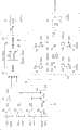
参照图3,根据本发明的混合式补偿电路20可以应用在各种类型的电源转换器,例如直流对直流电源转换器及PFC电源转换器。在混合式补偿电路20中,数字信号产生器22根据与电源转换器的输出电压相关的反馈信号Vfb1及参考值Vref1产生数字信号Sd,数字类比转换器(Digital-to-Analog Converter;DAC)24将数字信号Sd转换为类比的第一信号Va1,偏移注入器(offset injector)26提供可变偏移值偏移第一信号Va1产生第二信号Va2,低通滤波器(Low Pass Filter;LPF)28滤除第二信号Va2的高频成分产生第三信号Vcomp供稳定电源转换器的输出电压。混合式补偿电路20系模拟如图2所示的gm型补偿电路14。众所周知,gm型补偿电路14提供二极点及一零点,混合式补偿电路20同样可以提供二极点及一零点,详言之,数字信号产生器22及DAC 24可视为第一极点产生器提供第一极点,偏移注入器26可视为零点产生器提供零点,LPF 28可视为第二极点产生器提供第二极点。Referring to FIG. 3 , the
图4系混合式补偿电路20的第一实施例。为了实现低频的第一极点,使用数字信号产生器22及DAC 24模拟gm型补偿电路14的转导放大器16。图4的数字信号产生器22包括比较器30比较反馈信号Vfb1及参考值Vref1产生比较信号Sc1,反相器32将比较信号Sc1反相产生信号Sc2给控制器42,振荡器40提供时脉信号Clk给控制器42及升降计数器44,控制器42因应时脉信号Clk对信号Sc2取样,当取样结果表示反馈信号Vfb1大于参考值Vref1时,控制器42发出控制信号Down给升降计数器44以调降数字信号Sd一个位元,进而调降电源转换器的输出功率。当取样结果表示反馈信号Vfb1低于参考值Vref1时,控制器42发出控制信号Up给升降计数器44以调升数字信号Sd一个位元,进而调升电源转换器的输出功率。升降计数器44根据时脉信号Clk取样控制器42所输出的控制信号Up及Down以调整数字信号Sd。DAC 24将数字信号Sd转换为第一信号Va1。DAC 24系相当常见的电路,其内部电路及操作于此不再赘述。在时脉信号Clk为低频时,取样的频率较低,数字信号Sd的变化较缓慢,导致混合式补偿电路20输出的第三信号Vcomp变化缓慢,此效果如同gm型补偿电路14使用大电容C1及C2一样。FIG. 4 shows a first embodiment of the
在电源转换器发生负载暂态时,若混合式补偿电路20输出的第三信号Vcomp仍缓慢变化,将无法快速反应,造成输出电压Vo发生大的电压落差或过冲。为了改善此问题,图4的数字信号产生器22还包括磁滞比较器34比较反馈信号Vfb1及临界值VH1产生比较信号SH给控制器42,磁滞比较器36比较反馈信号Vfb1及临界值VL1产生比较信号SL给控制器42,以及运算转导放大器38放大反馈信号Vfb1及参考值Vref1之间的差值ΔV产生频率调整信号Sfm给振荡器40以调整时脉信号Clk的频率。当反馈信号Vfb1及参考值Vref1之间的差值ΔV增加时,频率调整信号Sfm将调高时脉信号Clk的频率以加快取样频率,进而加快数字信号Sd的变化以及加快第三信号Vcomp的扭转率(slew rate),当反馈信号Vfb1大于临界值VH1或小于临界值VL1时,磁滞比较器34或36送出比较信号SL或SH给振荡器40,以使时脉信号Clk的频率上升至最大值,进而使数字信号Sd以最大频率调升或调降。此外,在反馈信号Vfb1大于临界值VH1时,控制器42亦根据比较信号SL发出控制信号Down_limit给升降计数器44,使该升降计数器44以最大频率将数字信号Sd调降到最小值以提高第三信号Vcomp的扭转率,使电源转换器的输出功率快速减少,使输出电压快速地下降至预设准位。同样的,在反馈信号Vfb1小于临界值VL1时,控制器42根据比较信号SH发出控制信号Up_limit给升降计数器44,使该升降计数器44以最大频率将数字信号Sd调升到最大值,因而提高第三信号Vcomp的扭转率,使电源转换器的输出功率上升,使输出电压快速上升到预设准位。在其他实施例中,当反馈信号VFB1大于或小于临界值VH1或VL1时,使升降计数器44也可以立即将数字信号Sd调升到最小值或最大值。在发生负载暂态时,反馈信号Vfb1及参考值Vref1之间的差值ΔV增加,故控制器42及升降计数器44的取样频率加快,因此加快第三信号Vcomp的扭转率(slew rate),而且在反馈信号Vfb1大于临界值VH1或小于临界值VL1时可以使数字信号Sd立即或以最快频率下降到最小值或上升到最大值,故能有效改善电源转换器的负载暂态响应。When the load transient occurs in the power converter, if the third signal Vcomp output by the
图2的转导放大器16的电流-电压特性曲线如图5所示,从图2可得The current-voltage characteristic curve of the
Ce×Vcomp=Icomp×T, 公式1Ce×Vcomp=Icomp×T, Formula 1
其中Ce为电容C1及C2的等效电容,T为产生电流Icomp的时间。从公式1可进一步推得Where Ce is the equivalent capacitance of the capacitors C1 and C2, and T is the time for generating the current Icomp. It can be further deduced from formula 1 that
Icomp/Ce=Vcomp/T, 公式2Icomp/Ce=Vcomp/T,
由公式2可知电流Icomp及电容Ce决定一电压变化率dVcomp/dt,又电容Ce为定值,故电流Icomp正比于电压变化率dVcomp/dt,因此图5的Y轴也可以视为电压变化率dVcomp/dt。图3的数字信号产生器22及DAC 24模拟转导放大器16也可以得到类似的电压变化率,例如图6系图4的DAC 24的第一信号Va1的电压变化率dVa1/dt(即扭转率)对电压Vref1-Vfb1的特性曲线,反馈信号Vfb1在临界值VL1和VH1之间时和图5的曲线是一样的,在两端则有迟滞区域,当反馈信号Vfb1上升到大于临界值VH1时,数字信号Sd以最快取样频率被调降,故第一信号Va1具有最快负向电压变化率-dVa1/dt_max,直到反馈信号Vfb1下降到小于磁滞临界值Vhy2,第一信号Va1的电压变化率dVa1/dt才回到原来的水准;同样的,当反馈信号Vfb1下降到小于临界值VL1时,数字信号Sd以最快时脉信号Clk的频率被调升,故第一信号Va1具有最快正向电压变化率dVa1/dt_max,直到反馈信号Vfb1上升到大于磁滞临界值Vhy1,第一信号Va1的电压变化率dVa1/dt才回到原来的水准。From
在图4的实施例中,偏移注入器26包括电流源46及开关M1串联在电源端Vcc及电阻Rof的第一端54之间,电流源48及开关M2串联在电阻Rof的第一端54及地端GND之间,电流源50及开关M3串联在电源端Vcc及电阻Rof的第二端56之间,电流源52及开关M4串联在电阻Rof的第二端56及地端GND之间。开关M1及M4受控于来自控制器42的控制信号Down,开关M2及M3受控于来自控制器42的控制信号Up,藉控制开关M1、M2、M3及M4,可以决定电阻Rof上电流Iof的方向。电流源46、48、50及52根据来自运算转导放大器38的频率调整信号Sfm决定电流Iof的大小,进而决定可变偏移值Vof以偏移第一信号Va1产生第二信号Va2。由于频率调整信号Sfm系与反馈信号Vfb1及参考值Vref1之间的差值ΔV有关,因此可变偏移值Vof亦随差值ΔV变化。在其他实施例中,电流源46、48、50及52亦可改为根据其他与差值ΔV相关的信号来决定电流Iof。图4的低通滤波器28包括由电阻Rf及电容Cf组成的RC滤波器,对第二信号Va2滤波产生第三信号Vcomp。从控制回路的物理意义来看,gm补偿电路14的零点系作为相位领先(phase lead)补偿,而第二极点则类似低通滤波器,因此本发明的混合式补偿电路20利用偏移注入器44提供瞬间的电压变化来模拟零点的作用,并以RC滤波器实现第二极点。In the embodiment of FIG. 4 , the offset
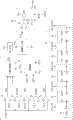
图7系图3的混合式补偿电路20的第二实施例,数字信号产生器22包括多工器60根据脉冲信号Sp1~Sp5依序将临界值VH1、临界值VH2、参考值Vref1、临界值VL2及临界值VL1提供给比较器62的非反相输入端,其中VH1>VH2>Vref1>VL2>VL1,比较器62的反相输入端接收反馈信号Vfb1,比较器62将反馈信号Vfb1分别比较临界值VH1、VH2、VL1及VL2及参考值Vref1,并将比较信号传送给控制器42,控制器42根据时脉信号Clk及脉冲信号Sp1~Sp5对比较器62所输出的比较信号取样,据以决定控制信号Up或Down给升降计数器44以调升或调降数字信号Sd,控制器42亦根据比较结果判断反馈信号Vfb1是否大于最大的临界值VH1或小于最小的临界值VL1,若反馈信号Vfb1大于临界值VH1,控制器42发出控制信号Down_limit使升降计数器44立即或以最大频率将数字信号Sd调降至最小值以加大第三信号Vcomp的扭转率,若反馈信号Vfb1小于临界值VL1,控制器42发出控制信号Up_limit使升降计数器44立即或以最大频率将数字信号Sd调升至最大值以加大第三信号Vcomp的扭转率。控制器42也根据比较结果决定频率调整信号Sfm给振荡器40以调整时脉信号Clk的频率,当反馈信号Vfb1与参考值Vref1之间的差值越大时,时脉信号Clk的频率越高,以加大第三信号Vcomp的扭转率,改善负载暂态响应。当反馈信号Vfb1大于临界值VH1或小于临界值VL1时,频率调整信号Sfm将使时脉信号Clk的频率调升至最大值,以加快控制器42及升降计数器44的取样频率。脉冲产生器64根据时脉信号Clk产生脉冲信号Sp1~Sp5如图8所示,在时脉信号Clk的每一个周期T内,脉冲产生器64依序产生脉冲信号Sp1~Sp5给多工器60。FIG. 7 is the second embodiment of the
图7的偏移注入器26系将图4的电阻Rof改为由开关控制之可变电阻,其阻值随反馈信号Vfb1及参考值Vref1之间的差值ΔV改变,电流源46、48、50及52提供固定电流,故通过可变电阻Rof的电流Iof系定值。在此实施中,可变电阻Rof包括三个串联的电阻Ra、Rb及Rc,每一个电阻Ra、Rb及Rc各与开关Ma、Mb及Mc并联,根据差值ΔV产生的信号Sa、Sb及Sc分别控制开关Ma、Mb及Mc以调整可变电阻Rof的阻值,进而产生随差值ΔV变化的可变偏移值Vof以偏移第一信号Va1产生第二信号Va2。The offset
图9系图7的DAC 24的第一信号Val的电压变化率dVa1/dt对电压Vref1-Vfb1的特性曲线,当反馈信号Vfb1上升到大于临界值VH1时,数字信号Sd以最快频率被调降,故第一信号Va1具有最快负向电压变化率-dVa1/dt_max,直到反馈信号Vfb1下降到小于临界值VH2,第一信号Va1的电压变化率才回到原来的水准;同样的,当反馈信号Vfb1下降到小于临界值VL1时,数字信号Sd以最快频率被调升,故第一信号Va1具有最快正向电压变化率dVa1/dt_max,直到反馈信号Vfb1上升到大于磁滞临界值VL2,第一信号Va1的变化速度才回到原来的水准。在图7的实施例中,随着设定的临界值个数的增加,图9的特性曲线将趋近于图6的特性曲线。Fig. 9 is the characteristic curve of the voltage change rate dVa1/dt of the first signal Val of the
图10系图3的混合式补偿电路20的第三实施例,数字信号产生器22包括比较器70比较反馈信号Vfb1及临界值VH1产生比较信号SB1,比较器72比较反馈信号Vfb1及临界值VH2产生比较信号SB2,比较器74比较反馈信号Vfb1及参考值Vref1产生比较信号SB3,比较器76比较反馈信号Vfb1及临界值VL2产生比较信号SB4,比较器78比较反馈信号Vfb1及临界值VL1产生比较信号SB5,控制器80根据比较信号SB1、SB2、SB3、SB4及SB5从时脉信号Clk1、Clk2、Clk3、Clk4及Clk5中选择其中一个作为时脉Clk给升降计数器44,当反馈信号Vfb1大于最大的临界值VH1或小于最小的临界值VL1时,控制器80选择频率最高的时脉信号Clk1给升降计数器44,升降计数器44因应时脉信号Clk对比较信号SB3取样,并根据取样结果调升或调降数字信号Sd一个位元,当反馈信号Vfb1大于最大的临界值VH1或小于最小的临界值VL1时,升降计数器44因应比较信号SB1或SB5立即或以最大频频将数字信号Sd调降至最小值或调升至最大值以加大第三信号Vcomp的扭转率,振荡器40提供具有频率f的时脉信号Clk1,除频器82对时脉信号Clk1除频产生具有频率f/2的时脉信号Clk2,除频器84对时脉信号Clk2除频产生具有频率f/4的时脉信号Clk3,除频器86对时脉信号Clk3除频产生具有频率f/8的时脉信号Clk4,除频器88对时脉信号Clk4除频产生具有频率f/16的时脉信号Clk5。在此混合式补偿电路中,DAC 24的第一信号Va1的电压变化率dVa1/dt对数字信号产生器22的输入电压Vfb1的特性曲线如图9所示。FIG. 10 is a third embodiment of the
图10的LPF 28包括低频宽的运算放大器90具有反相输入端接收来自偏移注入器26的第二信号Va2,以及非反相输入端连接LPF 28的输出端Vcomp,电阻R5及补偿电容C3串联在运算放大器90的输出端及LPF 28的输出端Vcomp之间,用以稳定第三信号Vcomp,晶体管M5连接在电源端Vcc及LPF 28的输出端Vcomp之间,晶体管M5的闸极连接运算放大器90的输出端,电阻R6连接在LPF 28的输出端Vcomp及地端GND之间。The
图11显示本发明的功效,使用图2的gm型类比式补偿电路14产生的电源转换器的输出电压Vo和信号Vcomp分别如波形92及96所示,使用本发明的混合式补偿电路20产生的电源转换器的输出电压Vo和第三信号Vcomp分别如波形94及98所示,其几乎与使用gm型类比式补偿电路14的效果相同,而且在时间t1所示的负载暂态发生时,也有良好的暂态响应,故混合式补偿电路20确实可以取代传统的类比式补偿电路14。混合式补偿电路20可以降低时脉信号Clk的频率来达成类比式补偿电路14中大电容C1及C2稳定信号Vcomp的功效,因此混合式补偿电路20无需使用大电容C1及C2,可以轻易的整合到控制IC中以减少接脚数量。混合式补偿电路20系混合类比电路及数字电路,因此相对于数字式补偿电路来说,混合式补偿电路20较简单,故占用较少的晶片面积,而且无需使用复杂DSP演算法,可简化设计及降低成本。Fig. 11 shows the effectiveness of the present invention. The output voltage Vo and signal Vcomp of the power converter generated by the gm type
Claims (30)
Applications Claiming Priority (2)
| Application Number | Priority Date | Filing Date | Title |
|---|---|---|---|
| TW100140680 | 2011-11-08 | ||
| TW100140680ATWI452810B (en) | 2011-11-08 | 2011-11-08 | Mixed mode compensation circuit and method for a power converter |
Publications (2)
| Publication Number | Publication Date |
|---|---|
| CN103095120Atrue CN103095120A (en) | 2013-05-08 |
| CN103095120B CN103095120B (en) | 2016-04-13 |
Family
ID=48207364
Family Applications (1)
| Application Number | Title | Priority Date | Filing Date |
|---|---|---|---|
| CN201110384178.7AActiveCN103095120B (en) | 2011-11-08 | 2011-11-28 | Hybrid Compensation Circuit and Method for Power Converter |
Country Status (3)
| Country | Link |
|---|---|
| US (1) | US9104216B2 (en) |
| CN (1) | CN103095120B (en) |
| TW (1) | TWI452810B (en) |
Cited By (2)
| Publication number | Priority date | Publication date | Assignee | Title |
|---|---|---|---|---|
| CN104868701A (en)* | 2014-02-21 | 2015-08-26 | 立锜科技股份有限公司 | Hybrid compensation circuit of power converter |
| CN105991011A (en)* | 2015-01-22 | 2016-10-05 | 立锜科技股份有限公司 | Control circuit and method for programming output voltage of power converter |
Families Citing this family (14)
| Publication number | Priority date | Publication date | Assignee | Title |
|---|---|---|---|---|
| US9541929B2 (en)* | 2012-11-08 | 2017-01-10 | Richtek Technology Corporation | Mixed mode compensation circuit |
| US8970260B1 (en)* | 2013-11-21 | 2015-03-03 | Nxp B.V. | Output drivers |
| JP6651697B2 (en)* | 2015-01-26 | 2020-02-19 | 株式会社ソシオネクスト | Electronic circuit, power supply circuit, method for measuring circuit characteristics, and program for calculating amplitude and phase characteristics |
| US9705412B2 (en)* | 2015-02-26 | 2017-07-11 | Stmicroelectronics S.R.L. | Pulsed feedback switching converter |
| TWI587619B (en)* | 2015-06-01 | 2017-06-11 | 立錡科技股份有限公司 | Power converter and switch control unit therein |
| US10782339B2 (en) | 2016-04-29 | 2020-09-22 | Teradyne, Inc. | Method and test system for providing accurate analog signals |
| EP3264311B1 (en)* | 2016-06-28 | 2021-01-13 | Eshard | A protection method and device against a side-channel analysis |
| US10996728B2 (en)* | 2019-01-04 | 2021-05-04 | Sigmasense, Llc. | Power supply signal conditioning system based on drive-sense circuit (DSC) processing |
| US11817785B2 (en)* | 2019-10-31 | 2023-11-14 | Renesas Electronics America Inc. | Device and method for controlling output voltage of a digital-to-analog converter |
| CN110971107A (en)* | 2019-12-20 | 2020-04-07 | 杰华特微电子(杭州)有限公司 | Switch circuit control method, control circuit and switch circuit |
| US11496144B2 (en)* | 2020-11-17 | 2022-11-08 | Centaur Technology, Inc. | Droop reference with programmable filter |
| CN113381617B (en) | 2021-06-29 | 2024-10-18 | 昂宝电子(上海)有限公司 | Constant voltage switching power supply and control chip and method thereof |
| TWI813070B (en)* | 2021-11-16 | 2023-08-21 | 瑞昱半導體股份有限公司 | Power supplying circuit and power supplying method |
| US12199627B2 (en)* | 2022-01-23 | 2025-01-14 | Samsung Display Co., Ltd. | Multi-purpose compensation circuits for high-speed receivers |
Citations (3)
| Publication number | Priority date | Publication date | Assignee | Title |
|---|---|---|---|---|
| US20020125872A1 (en)* | 2001-03-12 | 2002-09-12 | Groom Terry J. | Virtual ripple generation in switch-mode power supplies |
| US20080191678A1 (en)* | 2007-02-08 | 2008-08-14 | Infineon Technologies Austria Ag | Switch-mode converter |
| CN101789762A (en)* | 2010-01-15 | 2010-07-28 | 电子科技大学中山学院 | Configurable Current Pools in Tower Mounted Amplifiers |
Family Cites Families (8)
| Publication number | Priority date | Publication date | Assignee | Title |
|---|---|---|---|---|
| US6100827A (en)* | 1998-09-11 | 2000-08-08 | Ericsson Inc. | Modulation systems and methods that compensate for DC offset introduced by the digital-to-analog converter and/or the low pass filter thereof |
| JP3512156B2 (en)* | 1999-02-17 | 2004-03-29 | 松下電器産業株式会社 | Offset control circuit and offset control method |
| US6215433B1 (en)* | 1999-06-29 | 2001-04-10 | Oak Technology, Inc. | DC insensitive clock generator for optical PRML read channel |
| TW480379B (en)* | 2000-10-11 | 2002-03-21 | Mitsubishi Electric Corp | Offset compensation output control circuit and offset compensation output control method |
| JP3987294B2 (en)* | 2001-03-16 | 2007-10-03 | 株式会社東芝 | Offset compensation circuit |
| US7589983B1 (en)* | 2005-11-10 | 2009-09-15 | Iwatt Inc. | Power converter controller controlled by variable reference voltage generated by dual output digital to analog converter |
| US7973684B2 (en)* | 2008-10-27 | 2011-07-05 | Microchip Technology Incorporated | Self auto-calibration of analog circuits in a mixed signal integrated circuit device |
| JP5588407B2 (en)* | 2011-08-26 | 2014-09-10 | 株式会社東芝 | AD converter and DC-DC converter |
- 2011
- 2011-11-08TWTW100140680Apatent/TWI452810B/enactive
- 2011-11-28CNCN201110384178.7Apatent/CN103095120B/enactiveActive
- 2012
- 2012-11-08USUS13/672,125patent/US9104216B2/enactiveActive
Patent Citations (3)
| Publication number | Priority date | Publication date | Assignee | Title |
|---|---|---|---|---|
| US20020125872A1 (en)* | 2001-03-12 | 2002-09-12 | Groom Terry J. | Virtual ripple generation in switch-mode power supplies |
| US20080191678A1 (en)* | 2007-02-08 | 2008-08-14 | Infineon Technologies Austria Ag | Switch-mode converter |
| CN101789762A (en)* | 2010-01-15 | 2010-07-28 | 电子科技大学中山学院 | Configurable Current Pools in Tower Mounted Amplifiers |
Cited By (3)
| Publication number | Priority date | Publication date | Assignee | Title |
|---|---|---|---|---|
| CN104868701A (en)* | 2014-02-21 | 2015-08-26 | 立锜科技股份有限公司 | Hybrid compensation circuit of power converter |
| CN105991011A (en)* | 2015-01-22 | 2016-10-05 | 立锜科技股份有限公司 | Control circuit and method for programming output voltage of power converter |
| CN105991011B (en)* | 2015-01-22 | 2018-09-18 | 立锜科技股份有限公司 | Control circuit and method for programming output voltage of power converter |
Also Published As
| Publication number | Publication date |
|---|---|
| US20130113450A1 (en) | 2013-05-09 |
| CN103095120B (en) | 2016-04-13 |
| TW201320568A (en) | 2013-05-16 |
| US9104216B2 (en) | 2015-08-11 |
| TWI452810B (en) | 2014-09-11 |
Similar Documents
| Publication | Publication Date | Title |
|---|---|---|
| CN103095120B (en) | Hybrid Compensation Circuit and Method for Power Converter | |
| US10256724B2 (en) | Power supply controller | |
| CN112701889B (en) | Voltage regulator system, and method for ripple cancellation in a voltage regulator system | |
| CN114825926A (en) | Pulse width modulation controller for hybrid converter | |
| CN103683869A (en) | Switching power supply control circuit, switching power supply and control method of switching power supply | |
| TWI434499B (en) | Frequency jitter controller and frequency jitter control method for power converter | |
| CN101753024A (en) | Pwm clock generation system and method to improve transient response of a voltage regulator | |
| US9960675B2 (en) | Feed-forward control system with current estimator | |
| CN104734470A (en) | Constant On-Time Controller | |
| KR20140041108A (en) | Power supply circuit and hysteresis buck converter | |
| CN104868701A (en) | Hybrid compensation circuit of power converter | |
| TW201820067A (en) | Switching regulator synchronous node snubber circuit | |
| US10833665B2 (en) | Phase error correction for clock signals | |
| CN108347102A (en) | Wireless power supply transmitting circuit and control method thereof | |
| CN102468754A (en) | Control circuit and method for current mode control power converter | |
| TWI523391B (en) | Mixed mode compensation circuit | |
| CN106300978A (en) | Voltage converter | |
| US12431802B2 (en) | Multilevel buck converter with valley current mode control and dual slope compensation | |
| CN111796150B (en) | Duty cycle detection circuit and duty cycle detection method | |
| CN106787621B (en) | Compensation circuit and the control circuit for applying it | |
| TWI488418B (en) | Constant on-time controller | |
| CN108696276A (en) | Phase-adjusting circuit, inverter circuit and feed equipment | |
| CN118367760A (en) | Constant-time conduction circuit of equivalent series impedance compensation circuit and voltage conversion equipment | |
| TW202501971A (en) | Multi-level switching converter circuit and multi-level switching conversion method | |
| JP5928184B2 (en) | Power supply device, control circuit, electronic device, and power supply control method |
Legal Events
| Date | Code | Title | Description |
|---|---|---|---|
| C06 | Publication | ||
| PB01 | Publication | ||
| C10 | Entry into substantive examination | ||
| SE01 | Entry into force of request for substantive examination | ||
| C14 | Grant of patent or utility model | ||
| GR01 | Patent grant |