CN103094069A - Pixel structure and manufacturing method thereof - Google Patents
Pixel structure and manufacturing method thereofDownload PDFInfo
- Publication number
- CN103094069A CN103094069ACN2011104007059ACN201110400705ACN103094069ACN 103094069 ACN103094069 ACN 103094069ACN 2011104007059 ACN2011104007059 ACN 2011104007059ACN 201110400705 ACN201110400705 ACN 201110400705ACN 103094069 ACN103094069 ACN 103094069A
- Authority
- CN
- China
- Prior art keywords
- patterned
- transparent conductive
- electrode
- conductive layer
- layer
- Prior art date
- Legal status (The legal status is an assumption and is not a legal conclusion. Google has not performed a legal analysis and makes no representation as to the accuracy of the status listed.)
- Granted
Links
- 238000004519manufacturing processMethods0.000titleclaimsabstractdescription22
- 238000003860storageMethods0.000claimsabstractdescription43
- 239000003990capacitorSubstances0.000claimsabstractdescription36
- 229910052751metalInorganic materials0.000claimsdescription48
- 239000002184metalSubstances0.000claimsdescription48
- 238000000034methodMethods0.000claimsdescription25
- 239000004065semiconductorSubstances0.000claimsdescription23
- 239000010409thin filmSubstances0.000claimsdescription19
- 238000005530etchingMethods0.000claimsdescription16
- 229920002120photoresistant polymerPolymers0.000claimsdescription16
- 238000000059patterningMethods0.000claimsdescription11
- 230000005684electric fieldEffects0.000claimsdescription8
- 239000000758substrateSubstances0.000claimsdescription8
- 239000004973liquid crystal related substanceSubstances0.000claimsdescription7
- 238000000151depositionMethods0.000claims1
- 238000005516engineering processMethods0.000abstractdescription8
- 238000010586diagramMethods0.000description7
- 239000000463materialSubstances0.000description3
- AMGQUBHHOARCQH-UHFFFAOYSA-Nindium;oxotinChemical compound[In].[Sn]=OAMGQUBHHOARCQH-UHFFFAOYSA-N0.000description2
- 238000002834transmittanceMethods0.000description2
- 230000015572biosynthetic processEffects0.000description1
- 230000000694effectsEffects0.000description1
- 150000002500ionsChemical class0.000description1
- 238000012986modificationMethods0.000description1
- 230000004048modificationEffects0.000description1
Images


Classifications
- G—PHYSICS
- G02—OPTICS
- G02F—OPTICAL DEVICES OR ARRANGEMENTS FOR THE CONTROL OF LIGHT BY MODIFICATION OF THE OPTICAL PROPERTIES OF THE MEDIA OF THE ELEMENTS INVOLVED THEREIN; NON-LINEAR OPTICS; FREQUENCY-CHANGING OF LIGHT; OPTICAL LOGIC ELEMENTS; OPTICAL ANALOGUE/DIGITAL CONVERTERS
- G02F1/00—Devices or arrangements for the control of the intensity, colour, phase, polarisation or direction of light arriving from an independent light source, e.g. switching, gating or modulating; Non-linear optics
- G02F1/01—Devices or arrangements for the control of the intensity, colour, phase, polarisation or direction of light arriving from an independent light source, e.g. switching, gating or modulating; Non-linear optics for the control of the intensity, phase, polarisation or colour
- G02F1/13—Devices or arrangements for the control of the intensity, colour, phase, polarisation or direction of light arriving from an independent light source, e.g. switching, gating or modulating; Non-linear optics for the control of the intensity, phase, polarisation or colour based on liquid crystals, e.g. single liquid crystal display cells
- G02F1/133—Constructional arrangements; Operation of liquid crystal cells; Circuit arrangements
- G02F1/1333—Constructional arrangements; Manufacturing methods
- G02F1/1343—Electrodes
- G02F1/134309—Electrodes characterised by their geometrical arrangement
- G02F1/134363—Electrodes characterised by their geometrical arrangement for applying an electric field parallel to the substrate, i.e. in-plane switching [IPS]
- G—PHYSICS
- G02—OPTICS
- G02F—OPTICAL DEVICES OR ARRANGEMENTS FOR THE CONTROL OF LIGHT BY MODIFICATION OF THE OPTICAL PROPERTIES OF THE MEDIA OF THE ELEMENTS INVOLVED THEREIN; NON-LINEAR OPTICS; FREQUENCY-CHANGING OF LIGHT; OPTICAL LOGIC ELEMENTS; OPTICAL ANALOGUE/DIGITAL CONVERTERS
- G02F1/00—Devices or arrangements for the control of the intensity, colour, phase, polarisation or direction of light arriving from an independent light source, e.g. switching, gating or modulating; Non-linear optics
- G02F1/01—Devices or arrangements for the control of the intensity, colour, phase, polarisation or direction of light arriving from an independent light source, e.g. switching, gating or modulating; Non-linear optics for the control of the intensity, phase, polarisation or colour
- G02F1/13—Devices or arrangements for the control of the intensity, colour, phase, polarisation or direction of light arriving from an independent light source, e.g. switching, gating or modulating; Non-linear optics for the control of the intensity, phase, polarisation or colour based on liquid crystals, e.g. single liquid crystal display cells
- G02F1/133—Constructional arrangements; Operation of liquid crystal cells; Circuit arrangements
- G02F1/136—Liquid crystal cells structurally associated with a semi-conducting layer or substrate, e.g. cells forming part of an integrated circuit
- G02F1/1362—Active matrix addressed cells
- G02F1/136213—Storage capacitors associated with the pixel electrode
- H—ELECTRICITY
- H10—SEMICONDUCTOR DEVICES; ELECTRIC SOLID-STATE DEVICES NOT OTHERWISE PROVIDED FOR
- H10D—INORGANIC ELECTRIC SEMICONDUCTOR DEVICES
- H10D86/00—Integrated devices formed in or on insulating or conducting substrates, e.g. formed in silicon-on-insulator [SOI] substrates or on stainless steel or glass substrates
- H10D86/01—Manufacture or treatment
- H10D86/021—Manufacture or treatment of multiple TFTs
- H—ELECTRICITY
- H10—SEMICONDUCTOR DEVICES; ELECTRIC SOLID-STATE DEVICES NOT OTHERWISE PROVIDED FOR
- H10D—INORGANIC ELECTRIC SEMICONDUCTOR DEVICES
- H10D86/00—Integrated devices formed in or on insulating or conducting substrates, e.g. formed in silicon-on-insulator [SOI] substrates or on stainless steel or glass substrates
- H10D86/40—Integrated devices formed in or on insulating or conducting substrates, e.g. formed in silicon-on-insulator [SOI] substrates or on stainless steel or glass substrates characterised by multiple TFTs
- H10D86/481—Integrated devices formed in or on insulating or conducting substrates, e.g. formed in silicon-on-insulator [SOI] substrates or on stainless steel or glass substrates characterised by multiple TFTs integrated with passive devices, e.g. auxiliary capacitors
- H—ELECTRICITY
- H10—SEMICONDUCTOR DEVICES; ELECTRIC SOLID-STATE DEVICES NOT OTHERWISE PROVIDED FOR
- H10D—INORGANIC ELECTRIC SEMICONDUCTOR DEVICES
- H10D86/00—Integrated devices formed in or on insulating or conducting substrates, e.g. formed in silicon-on-insulator [SOI] substrates or on stainless steel or glass substrates
- H10D86/40—Integrated devices formed in or on insulating or conducting substrates, e.g. formed in silicon-on-insulator [SOI] substrates or on stainless steel or glass substrates characterised by multiple TFTs
- H10D86/60—Integrated devices formed in or on insulating or conducting substrates, e.g. formed in silicon-on-insulator [SOI] substrates or on stainless steel or glass substrates characterised by multiple TFTs wherein the TFTs are in active matrices
- G—PHYSICS
- G02—OPTICS
- G02F—OPTICAL DEVICES OR ARRANGEMENTS FOR THE CONTROL OF LIGHT BY MODIFICATION OF THE OPTICAL PROPERTIES OF THE MEDIA OF THE ELEMENTS INVOLVED THEREIN; NON-LINEAR OPTICS; FREQUENCY-CHANGING OF LIGHT; OPTICAL LOGIC ELEMENTS; OPTICAL ANALOGUE/DIGITAL CONVERTERS
- G02F2201/00—Constructional arrangements not provided for in groups G02F1/00 - G02F7/00
- G02F2201/40—Arrangements for improving the aperture ratio
Landscapes
- Physics & Mathematics (AREA)
- Nonlinear Science (AREA)
- Engineering & Computer Science (AREA)
- Crystallography & Structural Chemistry (AREA)
- Mathematical Physics (AREA)
- Chemical & Material Sciences (AREA)
- General Physics & Mathematics (AREA)
- Optics & Photonics (AREA)
- Microelectronics & Electronic Packaging (AREA)
- Power Engineering (AREA)
- Geometry (AREA)
- Liquid Crystal (AREA)
- Manufacturing & Machinery (AREA)
Abstract
Translated fromChineseDescription
Translated fromChinese技术领域technical field
本发明涉及一种液晶显示器的像素结构及其制造方法,具体而言是一种可提高面板开口率的像素结构及其制造方法。The invention relates to a pixel structure of a liquid crystal display and a manufacturing method thereof, in particular to a pixel structure capable of increasing the aperture ratio of a panel and a manufacturing method thereof.
背景技术Background technique
一般液晶显示器的像素结构中,必须配置储存电容来储存像素数据至下次更新的时间。所述储存电容通常是由两金属层夹置而形成,由于所述两金属层系不透光,因此所述储存电容的配置必须牺牲面板的开口率,使得开口率降低。In the pixel structure of a general liquid crystal display, a storage capacitor must be configured to store the pixel data until the next update time. The storage capacitor is usually formed by sandwiching two metal layers. Since the two metal layers are opaque, the configuration of the storage capacitor must sacrifice the aperture ratio of the panel, so that the aperture ratio is reduced.
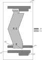
图1显示的是现有的像素结构的俯视图。图1所示的像素结构为一种平面内转换(in plane switching, IPS)架构的像素结构。所述像素结构由闸极线111及数据线151交错而形成,所述像素结构包含一薄膜晶体管结构19、一像素电极171、一共享电极181及一储存电容10。所述薄膜晶体管结构19包含一闸极113、一源极152和一汲极153。薄膜晶体管结构19的闸极113电性连接至闸极线111,源极152电性连接至数据线151。像素电极171透过一接触窗161与薄膜晶体管结构19的汲极153电性连接,共享电极181透过另一接触窗(未图示)与共享线112电性连接。像素电极171与共享电极181位在同一层,为IPS架构的电极配置,其两者间形成的电场可使液晶分子偏转。FIG. 1 shows a top view of a conventional pixel structure. The pixel structure shown in FIG. 1 is a pixel structure of an in plane switching (IPS) architecture. The pixel structure is formed by interlacing
储存电容10包含一下电极11和一上电极15,下电极11与上电极15之间设有一绝缘层(未图示),下电极11由共享线112往上下两侧延伸而形成,上电极15自汲极153延伸至下电极11上方。储存电容10的下电极11和上电极15皆为不透光的金属层,如前所述,此储存电容的配置会降低面板的开口率。The
另一方面,在像素结构的设计中,必须维持一定大小的储存电容,储存电容过小会导致馈通电压(feedthrough voltage)过大,而导致画面闪烁的情形发生。而在已知的像素结构中,增加储存电容势必需要增加上电极和下电极的面积,如此会使得开口率降低,而影响面板的品位。On the other hand, in the design of the pixel structure, it is necessary to maintain a certain size of the storage capacitor. If the storage capacitor is too small, the feedthrough voltage will be too large, resulting in flickering of the screen. In the known pixel structure, increasing the storage capacitor will inevitably increase the area of the upper electrode and the lower electrode, which will reduce the aperture ratio and affect the quality of the panel.
因此,如何开发一种像素结构,使其在维持一定大小的储存电容的情形下,能够不降低开口率,或更甚者能够提升开口率,实为目前产业界企须努力的方向。Therefore, how to develop a pixel structure so that it can maintain a certain size of the storage capacitor without reducing the aperture ratio, or even increase the aperture ratio, is the current direction that the industry must strive for.
发明内容Contents of the invention
本发明的第一目的在于提供一种像素结构及其制造方法,在不降低开口率的情形下增加储存电容来降低馈通电压,避免显示画面闪烁的情形发生。The first object of the present invention is to provide a pixel structure and its manufacturing method, which can reduce the feedthrough voltage by increasing the storage capacitance without reducing the aperture ratio, and avoid the flickering of the display screen.
本发明的另一目的在于提供一种像素结构及其制造方法,用以开发一种混合IPS与FFS技术的像素结构。Another object of the present invention is to provide a pixel structure and a manufacturing method thereof, which are used to develop a pixel structure combining IPS and FFS technologies.
为达前述目的,本发明提供一种像素结构的制造方法,包含:形成一图案化第一金属层于一基板上,所述图案化第一金属层包含一共享线及一闸极;形成一图案化第一透明导电层,所述图案化第一透明导电层的一部份覆盖所述共享线,以与所述共享线电性连接;形成一第一绝缘层以覆盖所述图案化第一金属层及所述图案化第一透明导电层;形成一图案化半导体层于所述闸极上方的第一绝缘层上;形成一图案化第二金属层,所述图案化第二金属层包含一源极及一汲极,其中所述源极与汲极分别位于所述图案化半导体层上的部份区域,所述闸极、图案化半导体层、源极及汲极构成一薄膜晶体管结构;形成一第二绝缘层;图案化所述第一绝缘层及所述第二绝缘层,以形成一第一接触窗及一第二接触窗;以及形成一图案化第二透明导电层,其包含一像素电极及一共享电极,其中所述像素电极透过所述第一接触窗与所述薄膜晶体管结构的汲极电性连接,所述共享电极透过所述第二接触窗与所述图案化第一透明导电层电性连接。To achieve the aforementioned purpose, the present invention provides a method for manufacturing a pixel structure, comprising: forming a patterned first metal layer on a substrate, the patterned first metal layer including a shared line and a gate; forming a Patterning the first transparent conductive layer, a part of the patterned first transparent conductive layer covers the shared line, so as to be electrically connected with the shared line; forming a first insulating layer to cover the patterned first A metal layer and the patterned first transparent conductive layer; forming a patterned semiconductor layer on the first insulating layer above the gate; forming a patterned second metal layer, the patterned second metal layer Including a source and a drain, wherein the source and the drain are respectively located in a part of the patterned semiconductor layer, the gate, the patterned semiconductor layer, the source and the drain form a thin film transistor structure; forming a second insulating layer; patterning the first insulating layer and the second insulating layer to form a first contact window and a second contact window; and forming a patterned second transparent conductive layer, It includes a pixel electrode and a shared electrode, wherein the pixel electrode is electrically connected to the drain of the thin film transistor structure through the first contact window, and the shared electrode is connected to the drain electrode through the second contact window. The patterned first transparent conductive layer is electrically connected.
本发明并提供一种像素结构,其是由一闸极线及一数据线所定义,所述像素结构包含:一共享线,提供一共同电压;一图案化第一透明导电层,其与所述共享线电性连接,并具有一第一共享电极,延伸至所述像素结构的显示区;一图案化第二透明导电层,位在所述图案化第一透明导电层上方,所述图案化第二透明导电层具有一像素电极及一第二共享电极;至少一绝缘层,设置于所述图案化第一透明导电层与所述图案化第二透明导电层之间;以及一薄膜晶体管结构,与所述图案化第一透明导电层及所述图案化第二透明导电层设置在相同的基板上,所述薄膜晶体管结构包含一闸极、一源极及一汲极,所述闸极电性连接至所述闸极线,所述源极电性连接至所述数据线;其中所述像素电极电性连接至所述薄膜晶体管结构的汲极,所述第二共享电极电性连接至所述第一共享电极,所述像素电极、第一共享电极及第二共享电极形成的电场会使液晶分子发生偏转,而且所述像素电极与所述第一共享电极间形成一储存电容。The present invention also provides a pixel structure, which is defined by a gate line and a data line, the pixel structure includes: a shared line, providing a common voltage; a patterned first transparent conductive layer, which is connected with the all The shared line is electrically connected, and has a first shared electrode, extending to the display area of the pixel structure; a patterned second transparent conductive layer, located above the patterned first transparent conductive layer, the pattern The second transparent conductive layer has a pixel electrode and a second shared electrode; at least one insulating layer is arranged between the patterned first transparent conductive layer and the patterned second transparent conductive layer; and a thin film transistor The structure is arranged on the same substrate as the patterned first transparent conductive layer and the patterned second transparent conductive layer, the thin film transistor structure includes a gate, a source and a drain, and the gate The electrode is electrically connected to the gate line, the source is electrically connected to the data line; wherein the pixel electrode is electrically connected to the drain of the thin film transistor structure, and the second shared electrode is electrically connected Connected to the first shared electrode, the electric field formed by the pixel electrode, the first shared electrode and the second shared electrode will deflect the liquid crystal molecules, and a storage capacitor is formed between the pixel electrode and the first shared electrode .
为避免画面闪烁,现有技术中需将两金属层所占面积增大,以获得较大的储存电容来降低馈通电压,如此会使得开口率下降。在本发明的像素结构中,储存电容主要是利用两透明导电层来形成,故可在不降低开口率的情形下增加储存电容来降低馈通电压,避免显示画面闪烁的情形发生。另一方面,本发明是一种混合IPS与FFS技术的像素结构,像素电极与第二共享电极类似于IPS架构的电极配置,而像素电极与第一共同电极类似于FFS架构的电极配置。In order to avoid screen flickering, in the prior art, the area occupied by the two metal layers needs to be increased to obtain a larger storage capacitor to reduce the feedthrough voltage, which will reduce the aperture ratio. In the pixel structure of the present invention, the storage capacitor is mainly formed by two transparent conductive layers, so the storage capacitor can be increased without reducing the aperture ratio to reduce the feed-through voltage and avoid the flickering of the display screen. On the other hand, the present invention is a mixed IPS and FFS technology pixel structure, the pixel electrode and the second shared electrode are similar to the electrode configuration of the IPS structure, and the pixel electrode and the first common electrode are similar to the electrode configuration of the FFS structure.
附图说明Description of drawings
下面结合附图和具体实施方式来详细说明本发明;The present invention is described in detail below in conjunction with accompanying drawing and specific embodiment;
图1是现有的像素结构的俯视图。FIG. 1 is a top view of a conventional pixel structure.
图2A是本发明像素结构的制造方法中形成一图案化第一金属层的示意图。2A is a schematic diagram of forming a patterned first metal layer in the manufacturing method of the pixel structure of the present invention.
图2B是图2A中沿A-B、C-D、E-F剖面线所绘制的剖面示意图。FIG. 2B is a schematic cross-sectional view drawn along section lines A-B, C-D, and E-F in FIG. 2A .
图3A是本发明像素结构的制造方法中形成一图案化第一透明导电层的示意图。3A is a schematic diagram of forming a patterned first transparent conductive layer in the manufacturing method of the pixel structure of the present invention.
图3B是图3A中沿A-B、C-D、E-F剖面线所绘制的剖面示意图。Fig. 3B is a schematic cross-sectional view drawn along the section lines A-B, C-D, and E-F in Fig. 3A.
图4A是本发明像素结构的制造方法中形成一图案化半导体层的示意图。FIG. 4A is a schematic diagram of forming a patterned semiconductor layer in the manufacturing method of the pixel structure of the present invention.
图4B是图4A中沿A-B、C-D、E-F剖面线所绘制的剖面示意图。Fig. 4B is a schematic cross-sectional view drawn along the section lines A-B, C-D, and E-F in Fig. 4A.
图5A是本发明像素结构的制造方法中形成一图案化第二金属层的示意图。5A is a schematic diagram of forming a patterned second metal layer in the manufacturing method of the pixel structure of the present invention.
图5B是图5A中沿A-B、C-D、E-F剖面线所绘制的剖面示意图。FIG. 5B is a schematic cross-sectional view drawn along the A-B, C-D, and E-F section lines in FIG. 5A .
图6A是本发明像素结构的制造方法中图案化第一绝缘层及一第二绝缘层的示意图。6A is a schematic diagram of patterning a first insulating layer and a second insulating layer in the manufacturing method of the pixel structure of the present invention.
图6B是图6A中沿A-B、C-D、E-F剖面线所绘制的剖面示意图。FIG. 6B is a schematic cross-sectional view drawn along the A-B, C-D, and E-F section lines in FIG. 6A .
图7A是本发明像素结构的制造方法中形成一图案化第二透明导电层的示意图。7A is a schematic diagram of forming a patterned second transparent conductive layer in the manufacturing method of the pixel structure of the present invention.
图7B是图7A中沿A-B、C-D、E-F剖面线所绘制的剖面示意图。Fig. 7B is a schematic cross-sectional view drawn along the section lines A-B, C-D, and E-F in Fig. 7A.
图8A是本发明另一较佳实施例的像素结构的俯视图。FIG. 8A is a top view of a pixel structure in another preferred embodiment of the present invention.
图8B是图8A所示的像素结构的剖面示意图。FIG. 8B is a schematic cross-sectional view of the pixel structure shown in FIG. 8A .
图8C是图8A中图案化第一透明导电层的示意图。FIG. 8C is a schematic diagram of patterning the first transparent conductive layer in FIG. 8A .
其中:in:
10 储存电容 11 下电极10 Storage Capacitor 11 Lower Electrode
15 上电极 19 薄膜晶体管结构15
111 闸极线 112 共享线
113 闸极 151 资料线113
152 源极 153 汲极152
161 接触窗 171 像素电极161
181 共享电极 25 上电极
21 下电极 28 薄膜晶体管结构21
201 基板 210 图案化第一金属层201
211 闸极线 212 共享线
213 闸极 220 图案化第一透明导电层213
220a 图案化第一透明导电层 230 第一绝缘层220a Patterning the first transparent
240 图案化半导体层 241 半导体通道层240 Patterned semiconductor layer 241 Semiconductor channel layer
242 奥姆接触层 250 图案化第二金属层242
251 资料线 252 源极
253 汲极 260 第二绝缘层253
261 第一接触窗 262 第二接触窗261
270 图案化第二透明导电层 271 像素电极270 Patterning the second transparent
272 共享电极。272 shared electrodes.
具体实施方式Detailed ways
为了使本发明实现的技术手段、创作特征、达成目的与功效易于明白了解,下面结合具体图示,进一步阐述本发明。In order to make the technical means, creative features, goals and effects achieved by the present invention easy to understand, the present invention will be further described below in conjunction with specific illustrations.
本发明一种液晶显示器,包含数个像素结构,本发明的特点在于各像素结构是利用两透明导电层来形成储存电容(storage capacitor, Cst),并且本发明的像素结构是一种混合平面内转换(in plane switching, IPS)技术和边缘场切换(fringe field switching, FFS)技术而实现的像素结构,兹将各像素的具体结构及其制造方法详述如下。A liquid crystal display of the present invention includes several pixel structures. The feature of the present invention is that each pixel structure utilizes two transparent conductive layers to form a storage capacitor (storage capacitor, Cst), and the pixel structure of the present invention is a hybrid in-plane The pixel structure realized by in plane switching (IPS) technology and fringe field switching (FFS) technology, the specific structure and manufacturing method of each pixel are described in detail as follows.
本发明揭露一种像素结构及其制造方法,本发明的像素结构显示于图7A及图7B,其中图7A是本发明的像素结构的俯视图,图7B是本发明的像素结构的剖面示意图。本发明揭露的像素结构的制造方法请参阅图2A至图7B,其中剖面图是沿着A-B、C-D及E-F剖面线所绘制。The present invention discloses a pixel structure and a manufacturing method thereof. The pixel structure of the present invention is shown in FIGS. 7A and 7B , wherein FIG. 7A is a top view of the pixel structure of the present invention, and FIG. 7B is a schematic cross-sectional view of the pixel structure of the present invention. Please refer to FIG. 2A to FIG. 7B for the manufacturing method of the pixel structure disclosed in the present invention, wherein the cross-sectional views are drawn along the A-B, C-D and E-F cross-section lines.
请参阅图2A及图2B,首先,利用第一道微影蚀刻制程(photolithographic etching process, PEP)在基板201上形成一图案化第一金属层210,图案化第一金属层210包含一共享线212和一闸极213。需注意的是,在形成图案化第一金属层210的步骤中,图案化第一金属层210也可以包含一闸极线211,闸极213为闸极线211的一部份,或者闸极线211的一部份用作闸极213,闸极线211与闸极213实质上是电性连接的。闸极线211、共享线212与门极213都是用相同的材料且在同一制程步骤中形成。具体来说,在形成图案化第一金属层210的步骤中,首先沉积一第一金属层于基板201上,而后形成一第一图案化光阻层(未图示)于所述第一金属层上,接着进行蚀刻制程,以形成如图2A所示的共享线212和闸极213,且形成闸极线211,最后再移除所述第一图案化光阻层。Please refer to FIG. 2A and FIG. 2B. First, a patterned
请参阅图3A及图3B,接着,利用第二道微影蚀刻制程,形成一图案化第一透明导电层220,其中图案化第一透明导电层220的一部份覆盖共享线212,与共享线212电性连接。在本发明中,图案化第一透明导电层220是用作像素结构的储存电容的其中一个电极,同时亦用作IPS及FFS架构的共享电极(容后详述)。具体来说,在形成图案化第一透明导电层220的步骤中,首先沉积一第一透明导电层,如铟锡氧化物(indium tin oxide, ITO),而后形成一第二图案化光阻层(未图示)于所述第一透明导电层上,接着进行蚀刻制程,以形成如图3A及图3B所示的图案化第一透明导电层220,最后再移除所述第二图案化光阻层。如图3A所示,图案化第一透明导电层220的一部份与共享线212重叠,并且图案化第一透明导电层220自共享线212的一部份延伸至像素结构的显示区。Please refer to FIG. 3A and FIG. 3B , and then, a second patterned transparent
请参阅图4A及图4B,在形成图案化第一透明导电层220后,接着形成一第一绝缘层230以覆盖上述的图案化第一金属层210及图案化第一透明导电层220,如图4B所示。需注意的是,第一绝缘层230未显示于图4A中。接下来进行第三道微影蚀刻制程,以形成一图案化半导体层240于闸极213上方的第一绝缘层230上。在一实施例中,图案化半导体层240可包含半导体通道层241(又称为主动层)及奥姆接触层242,如图4B所示。在第三道微影蚀刻制程中,可先沉积半导体层240,接着再植入N+离子,或者直接沉积掺杂的半导体材料层于半导体通道层241上,以在半导体通道层241上形成奥姆接触层242。然后,形成第三图案化光阻层(未图示)于奥姆接触层242上,再进行蚀刻制程,保留对应于闸极213上方区域的半导体信道层241及奥姆接触层242,最后再移除所述第三图案化光阻层,便可形成图案化半导体层240。Please refer to FIG. 4A and FIG. 4B, after forming the patterned first transparent
请参阅图5A及图5B,本发明利用第四道微影蚀刻制程形成一图案化第二金属层250,图案化第二金属层250包含一源极252及一汲极253,如图5B所示,其中源极252和汲极253分别位于图案化半导体层240的奥姆接触层242的部份上,闸极213、图案化半导体层240、源极252及汲极253构成一薄膜晶体管结构28。需注意的是,在形成图案化第二金属层250的步骤中,图案化第二金属层250也可以包含一数据线251(如第5A图所示),源极252为数据线251的一部份,或者资料线251的一部份用作源极252,资料线251与源极252实质上是电性连接的。数据线251及源极252都是用相同的材料且在同一制程步骤中形成。在一实施例中,在形成图案化第二金属层250的步骤中,图案化第二金属层250并在第一绝缘层230上从汲极253延伸至共享线212上方的部份区域形成一上电极25,而共享线212的一部份作为一下电极21,如图5A所示,上电极25与下电极21彼此绝缘且构成一电容(容后详述)。具体来说,在形成图案化第二金属层250的步骤中,首先沉积一第二金属层,而后形成一第四图案化光阻层(未图示)于所述第二金属层上,接着进行蚀刻制程,去除部份的第二金属层,以在奥姆接触层242的部份区域上形成源极252及汲极253,且可一并形成数据线251及上电极25,最后再移除所述第四图案化光阻层。Please refer to FIG. 5A and FIG. 5B, the present invention utilizes the fourth lithographic etching process to form a patterned
请参阅图6A及图6B,在形成图案化第二金属层250后,接着沉积形成一第二绝缘层260,然后利用第五道微影蚀刻制程图案化第一绝缘层230及第二绝缘层260,以形成一第一接触窗261及一第二接触窗262,如图6A及图6B所示。需注意的是,第二绝缘层260未显示于图6A中。具体来说,图案化第一绝缘层230及第二绝缘层260的步骤包含:形成一第五图案化光阻层(未图示)于第二绝缘层260上,接着进行蚀刻制程,去除部份的第二绝缘层260及第一绝缘层230,以形成第一接触窗261暴露出图案化第二金属层250中与汲极253电性连接的部份,并形成第二接触窗262以暴露出部份图案化第一透明导电层220,最后再移除所述第五图案化光阻层。在一实施例中,上述图案化第二金属层250中与汲极253电性连接的部份是位于共享线212上方的部份区域。Please refer to FIG. 6A and FIG. 6B. After forming the patterned
请参阅图7A及图7B,本发明最后利用第六道微影蚀刻制程形成一图案化第二透明导电层270,其包含一像素电极271及一共享电极272,其中像素电极271系透过第一接触窗261与所述薄膜晶体管结构28的汲极253电性连接,而共享电极272是透过第二接触窗262与图案化第一透明导电层220电性连接,如图7A及图7 B所示。需注意的是,图7A中被图案化第二透明导电层270覆盖的下方组件以虚线表示。具体来说,在形成图案化第二透明导电层270的步骤中,先沉积一第二透明导电层,如铟锡氧化物,再形成一第六图案化光阻层(未图示)于所述第二透明导电层上,接着进行蚀刻制程,以形成像素电极271及共享电极272,最后再移除所述第六图案化光阻层。如图7A所示,共享电极272具有一U型狭缝,像素电极271具有一U型结构,其U型结构支脚延伸至像素结构的显示区,且位在共享电极272的U型狭缝内。在其它实施例中,共享电极272亦可具有其它类型的狭缝,而像素电极271则具有对应这些类型的狭缝的结构。Please refer to FIG. 7A and FIG. 7B. Finally, the present invention uses the sixth lithographic etching process to form a patterned second transparent
如前所述,图案化第二透明导电层270的共享电极272系与图案化第一透明导电层220电性连接,因此图案化第一透明导电层220的电位与共享电极272相同而可视为另一共同电极。本发明中,像素电极271与共享电极272类似于IPS架构的电极配置,可形成水平电场,而像素电极271与该另一共同电极(即图案化第一透明导电层220)则类似于FFS架构的电极配置,可形成边缘电场,因此本发明是一种混合IPS与FFS技术的像素结构。再者,彼此绝缘设置的图案化第一透明导电层220与图案化第二透明导电层270中的像素电极271是形成本发明的像素结构的储存电容。由于本发明的像素结构的储存电容是由两透明导电层所形成,相较于现有技术中以两金属层夹置来形成储存电容,本发明不会因形成储存电容而影响面板的开口率,因此本发明在不降低开口率的情形下,可有效降低馈通电压(feedthrough voltage),避免画面闪烁。此外,另一方面,共享线212的一部份所形成的下电极21及对应共享线212上方部份区域的图案化第二金属层250所形成的上电极25,两者所构成的电容的电容值亦对本发明上述的储存电容有所贡献。As mentioned above, the shared
本发明另一较佳实施例中,在利用第二道微影蚀刻制程形成图案化第一透明导电层的过程中,可形成如图8C所示的图案化第一透明导电层220a,其对应图案化第二透明导电层270的共享电极272设置有一镂空结构,其有助于增加透光度。除此之外,其余制程与第2、4~7图类似,在此不再赘述。本发明另一较佳实施例的像素结构的上视示意图及剖面示意图分别显示于图8A及图8B。In another preferred embodiment of the present invention, in the process of forming the patterned first transparent conductive layer using the second lithographic etching process, the patterned first transparent
请参阅图7A及图7B,本发明的像素结构由闸极线211及数据线251交错而形成,其是由闸极线211和数据线251所定义。所述像素结构包含一共享线212、一图案化第一透明导电层220、一图案化第二透明导电层270、至少一绝缘层230、260及一薄膜晶体管结构28,这些组件都设置在同一基板201上。闸极线221提供扫描讯号,数据线251提供像素数据,而共享线212则用以提供共同电压。需注意的是,图7A中被图案化第二透明导电层270覆盖的下方组件以虚线表示。Please refer to FIG. 7A and FIG. 7B , the pixel structure of the present invention is formed by interlacing
图案化第一透明导电层220是延伸至所述像素结构的显示区以形成一第一共享电极,所述第一共享电极是与共享线212电性连接。在一实施例中,图案化第一透明导电层220的一部份是与共享线212直接重叠,使得所述第一共享电极电性连接至共享线212。图案化第二透明导电层270位在图案化第一透明导电层220上方,图案化第一透明导电层220与图案化第二透明导电层270之间设置有至少一所述绝缘层230、260。图案化第二透明导电层270形成有一像素电极271及一第二共享电极272。如图7A所示,第二共享电极272具有数个狭缝,像素电极271具有一U型结构,所述U型结构的支脚延伸至所述像素结构的显示区,且位于第二共享电极272的狭缝内。The patterned first transparent
薄膜晶体管结构28包含一闸极213、一源极252及一汲极253,闸极213电性连接至闸极线221,源极253电性连接至数据线251。再者,图案化第二透明导电层270的像素电极271电性连接至薄膜晶体管结构28的汲极253。在一实施例中,图案化第二透明导电层270的像素电极271是透过一第一接触窗261而与薄膜晶体管结构28的汲极253电性连接。图案化第一透明导电层220的第一共享电极电性连接至图案化第二透明导电层270的第二共享电极272,亦即所述第一共享电极与第二共享电极272的电位相同。在一实施例中,图案化第二透明导电层270的第二共同电极272是透过一第二接触窗262而与图案化第一透明导电层220的第一共同电极电性连接。The
本发明中,图案化第二透明导电层270的像素电极271会分别与第一共享电极和第二共享电极272形成电场而使液晶分子发生偏转。详言之,图案化第二透明导电层270中的像素电极271与第二共享电极272类似于IPS架构的电极配置,可形成水平电场;而图案化第二透明导电层270的像素电极271与图案化第一透明导电层220的第一共同电极类似于FFS架构的电极配置,可形成边缘电场,因此本发明是一种混合IPS与FFS技术的像素结构,具有广视角、低耗电及低色偏等优势。In the present invention, the
再者,如前所述,图案化第一透明导电层220与图案化第二透明导电层270设置有至少一所述绝缘层230、260,彼此绝缘设置的像素电极271与所述第一共享电极会形成本发明的像素结构的第一储存电容。此外,本发明的像素结构更包含一金属层,其自薄膜晶体管结构28的汲极253延伸至共享线212上方的部份区域形成一上电极25,而共享线212的部份区域形成一下电极21,上电极25与下电极21会构成本发明的像素结构的第二储存电容。本发明像素结构的储存电容的有效电容值是由第一储存电容与第二储存电容的电容值相加而得。相较于现有技术中仅以两金属层夹置来形成储存电容,本发明是将两金属层所占面积缩小来提高开口率,同时利用两透明导电层形成的电容来补偿因两金属层面积缩小而减少的电容。举例来说,在相同的馈通电压下,储存电容的有效电容值为121fF,图1所示的现有的像素结构其开口率为36.75%,而图7A及图7B所示的本发明像素结构的开口率为41.02%,两者开口率差异达到10%左右,可见本发明的像素结构在不降低储存电容的情形下,能够有效提高开口率。Furthermore, as mentioned above, the patterned first transparent
由上,现有技术中仅以两金属层夹置来形成储存电容,当馈通电压增大时,需要较大的储存电容以避免画面闪烁,而已知需将两金属层所占面积增大以获得较大的储存电容,如此使得开口率下降。本发明的像素结构的储存电容主要是利用两透明导电层来形成,故可在不降低开口率的情形下增加储存电容,馈通电压会因储存电容增加而下降,因此可减轻显示画面闪烁的情形发生。From the above, in the prior art, only two metal layers are sandwiched to form a storage capacitor. When the feed-through voltage increases, a larger storage capacitor is required to avoid screen flickering, and it is known that the area occupied by the two metal layers needs to be increased. In order to obtain a larger storage capacitance, the aperture ratio is reduced. The storage capacitance of the pixel structure of the present invention is mainly formed by two transparent conductive layers, so the storage capacitance can be increased without reducing the aperture ratio, and the feedthrough voltage will decrease due to the increase of the storage capacitance, so the flickering of the display screen can be reduced. Situation happens.
此外,在一实施例中,共享线212、闸极线211与薄膜晶体管28的闸极213可在同一制程中形成,因而共享线212、闸极线211与闸极213位在同一层。在一实施例中,闸极213与闸极线211可在同一制程中形成,源极252与资料线251可在另一制程中形成,因而闸极213与闸极线211位在同一层,而源极252与资料线251同属于另一层。在另一实施例中,薄膜晶体管结构28更包含一半导体层240,如前所述,半导体层240包含一半导体通道层241及一奥姆接触层242。In addition, in one embodiment, the
本发明另一较佳实施例中,可形成如图8C所示的图案化第一透明导电层220a作为所述第一共享电极,其对应图案化第二透明导电层270的第二共享电极272设置有一镂空结构,其有助于增加透光度。本发明另一较佳实施例的像素结构的俯视图及剖面示意图分别显示于图8A及图8B。In another preferred embodiment of the present invention, the patterned first transparent
综上所述,虽然本发明已用较佳实施例揭露如上,然其并非用以限定本发明,本发明所属技术领域中具有通常知识者,在不脱离本发明之精神和范围内,当可作各种之更动与润饰,因此本发明之保护范围当视后附之申请专利范围所界定者为准。In summary, although the present invention has been disclosed as above with preferred embodiments, it is not intended to limit the present invention. Those with ordinary knowledge in the technical field of the present invention can, without departing from the spirit and scope of the present invention, Various changes and modifications are made, so the scope of protection of the present invention should be defined by the scope of the appended patent application.
Claims (10)
Translated fromChineseApplications Claiming Priority (2)
| Application Number | Priority Date | Filing Date | Title |
|---|---|---|---|
| TW100140628ATWI474092B (en) | 2011-11-07 | 2011-11-07 | Pixel structure and its manufacturing method |
| TW100140628 | 2011-11-07 |
Publications (2)
| Publication Number | Publication Date |
|---|---|
| CN103094069Atrue CN103094069A (en) | 2013-05-08 |
| CN103094069B CN103094069B (en) | 2016-04-20 |
Family
ID=48206503
Family Applications (1)
| Application Number | Title | Priority Date | Filing Date |
|---|---|---|---|
| CN201110400705.9AActiveCN103094069B (en) | 2011-11-07 | 2011-12-06 | Pixel structure |
Country Status (3)
| Country | Link |
|---|---|
| US (1) | US9081241B2 (en) |
| CN (1) | CN103094069B (en) |
| TW (1) | TWI474092B (en) |
Cited By (5)
| Publication number | Priority date | Publication date | Assignee | Title |
|---|---|---|---|---|
| CN103353695A (en)* | 2013-06-28 | 2013-10-16 | 北京京东方光电科技有限公司 | Array substrate and display device |
| CN103700671A (en)* | 2013-12-24 | 2014-04-02 | 华映视讯(吴江)有限公司 | Pixel array substrate and display panel |
| CN104423107A (en)* | 2013-08-29 | 2015-03-18 | 乐金显示有限公司 | Liquid crystal display device and febrication method thereof |
| WO2016045423A1 (en)* | 2014-09-23 | 2016-03-31 | Boe Technology Group Co., Ltd. | Array substrate, fabrication method thereof and display device |
| CN107578700A (en)* | 2017-08-03 | 2018-01-12 | 友达光电股份有限公司 | Pixel structure |
Families Citing this family (3)
| Publication number | Priority date | Publication date | Assignee | Title |
|---|---|---|---|---|
| KR102262431B1 (en) | 2015-02-03 | 2021-06-08 | 삼성디스플레이 주식회사 | Liquid crystal display |
| CN105116642B (en)* | 2015-09-24 | 2018-07-17 | 京东方科技集团股份有限公司 | Array substrate and preparation method thereof, display device |
| CN107229168A (en)* | 2017-06-01 | 2017-10-03 | 昆山龙腾光电有限公司 | The array base palte and display device of display panel |
Citations (4)
| Publication number | Priority date | Publication date | Assignee | Title |
|---|---|---|---|---|
| US20010050745A1 (en)* | 2000-06-07 | 2001-12-13 | Biing-Der Liu | In-plane switching liquid crystal displaying device and method of fabricating the same |
| CN1619393A (en)* | 2003-11-11 | 2005-05-25 | Lg.菲利浦Lcd株式会社 | Coplanar switching mode liquid crystal display device and manufacturing method thereof |
| US20060145990A1 (en)* | 2004-12-31 | 2006-07-06 | Lg.Philips Lcd Co., Ltd. | In-plane switching mode liquid crystal display device |
| CN101470308A (en)* | 2007-12-25 | 2009-07-01 | 瀚宇彩晶股份有限公司 | Liquid crystal display with high aperture ratio |
Family Cites Families (13)
| Publication number | Priority date | Publication date | Assignee | Title |
|---|---|---|---|---|
| KR100344844B1 (en)* | 1998-07-07 | 2002-11-18 | 엘지.필립스 엘시디 주식회사 | A Liquid Crystal Display Device And The Method For Manufacturing The Same |
| CN100371813C (en)* | 2003-10-14 | 2008-02-27 | Lg.菲利浦Lcd株式会社 | Liquid crystal display panel in in-plane switching liquid crystal display device and manufacturing method thereof |
| KR101127822B1 (en)* | 2004-12-24 | 2012-03-26 | 엘지디스플레이 주식회사 | Thin film transistor substrate of horizontal electric field and fabricating method thereof |
| KR20060078713A (en) | 2004-12-30 | 2006-07-05 | 엘지.필립스 엘시디 주식회사 | Transverse electric field liquid crystal display device |
| JP4385993B2 (en)* | 2005-05-10 | 2009-12-16 | 三菱電機株式会社 | Liquid crystal display device and manufacturing method thereof |
| EP1793266B1 (en)* | 2005-12-05 | 2017-03-08 | Semiconductor Energy Laboratory Co., Ltd. | Transflective Liquid Crystal Display with a Horizontal Electric Field Configuration |
| TWI545380B (en)* | 2006-05-16 | 2016-08-11 | 半導體能源研究所股份有限公司 | Liquid crystal display device and semiconductor device |
| KR101254828B1 (en)* | 2007-10-05 | 2013-04-15 | 엘지디스플레이 주식회사 | Liquid crystal display device |
| TWI356263B (en)* | 2007-11-30 | 2012-01-11 | Hannstar Display Corp | Liquid crystal display with high aperture ratio |
| JP5771365B2 (en) | 2009-11-23 | 2015-08-26 | 三星ディスプレイ株式會社Samsung Display Co.,Ltd. | Medium and small liquid crystal display |
| KR101735386B1 (en)* | 2010-06-25 | 2017-05-30 | 엘지디스플레이 주식회사 | Liquid crystal display device having touch sensor embedded therein, method for driving the same and method for fabricating the same |
| KR101866946B1 (en)* | 2010-11-02 | 2018-06-14 | 삼성디스플레이 주식회사 | Thin film transistor array panel and the method for manufacturing thereof |
| KR101298613B1 (en)* | 2010-12-27 | 2013-08-26 | 엘지디스플레이 주식회사 | Method for fabricating array substrate for in plane switching mode liquid crystal display device |
- 2011
- 2011-11-07TWTW100140628Apatent/TWI474092B/enactive
- 2011-12-06CNCN201110400705.9Apatent/CN103094069B/enactiveActive
- 2012
- 2012-01-20USUS13/355,481patent/US9081241B2/enactiveActive
Patent Citations (4)
| Publication number | Priority date | Publication date | Assignee | Title |
|---|---|---|---|---|
| US20010050745A1 (en)* | 2000-06-07 | 2001-12-13 | Biing-Der Liu | In-plane switching liquid crystal displaying device and method of fabricating the same |
| CN1619393A (en)* | 2003-11-11 | 2005-05-25 | Lg.菲利浦Lcd株式会社 | Coplanar switching mode liquid crystal display device and manufacturing method thereof |
| US20060145990A1 (en)* | 2004-12-31 | 2006-07-06 | Lg.Philips Lcd Co., Ltd. | In-plane switching mode liquid crystal display device |
| CN101470308A (en)* | 2007-12-25 | 2009-07-01 | 瀚宇彩晶股份有限公司 | Liquid crystal display with high aperture ratio |
Cited By (10)
| Publication number | Priority date | Publication date | Assignee | Title |
|---|---|---|---|---|
| CN103353695A (en)* | 2013-06-28 | 2013-10-16 | 北京京东方光电科技有限公司 | Array substrate and display device |
| WO2014206052A1 (en)* | 2013-06-28 | 2014-12-31 | 北京京东方光电科技有限公司 | Array substrate and display device |
| CN103353695B (en)* | 2013-06-28 | 2015-12-09 | 北京京东方光电科技有限公司 | A kind of array base palte and display device |
| US9488881B2 (en) | 2013-06-28 | 2016-11-08 | Boe Technology Group Co., Ltd. | Array substrate and display device |
| CN104423107A (en)* | 2013-08-29 | 2015-03-18 | 乐金显示有限公司 | Liquid crystal display device and febrication method thereof |
| CN104423107B (en)* | 2013-08-29 | 2017-08-22 | 乐金显示有限公司 | Liquid crystal disply device and its preparation method |
| CN103700671A (en)* | 2013-12-24 | 2014-04-02 | 华映视讯(吴江)有限公司 | Pixel array substrate and display panel |
| WO2016045423A1 (en)* | 2014-09-23 | 2016-03-31 | Boe Technology Group Co., Ltd. | Array substrate, fabrication method thereof and display device |
| US10418383B2 (en) | 2014-09-23 | 2019-09-17 | Boe Technology Group Co., Ltd. | Array substrate, fabrication method thereof and display device |
| CN107578700A (en)* | 2017-08-03 | 2018-01-12 | 友达光电股份有限公司 | Pixel structure |
Also Published As
| Publication number | Publication date |
|---|---|
| TWI474092B (en) | 2015-02-21 |
| US20130112983A1 (en) | 2013-05-09 |
| TW201319701A (en) | 2013-05-16 |
| US9081241B2 (en) | 2015-07-14 |
| CN103094069B (en) | 2016-04-20 |
Similar Documents
| Publication | Publication Date | Title |
|---|---|---|
| CN103094069B (en) | Pixel structure | |
| US7978294B2 (en) | Liquid crystal display device | |
| US8218117B2 (en) | Liquid crystal display and method of manufacturing the same | |
| KR101321218B1 (en) | Tft substrate and method for manufacture thereof | |
| CN100580536C (en) | Array substrate of liquid crystal display device and manufacturing method thereof | |
| CN102881688B (en) | Array substrate, display panel and array substrate manufacturing method | |
| US20120050643A1 (en) | Array substrate, liquid crystal panel and liquid crystal display | |
| CN100362414C (en) | Coplanar switching mode liquid crystal display device and manufacturing method thereof | |
| JP4999875B2 (en) | Multi-domain liquid crystal display device | |
| CN102200665B (en) | High light transmittance in-plane switching liquid crystal display device and manufacture method thereof | |
| JP2003195330A (en) | Liquid crystal display | |
| US9097951B2 (en) | Thin film transistor array substrate and method for manufacturing the same, and liquid crystal display device | |
| WO2017054394A1 (en) | Array substrate and manufacturing method therefor, and display device | |
| US9978880B2 (en) | Display device | |
| CN103488012B (en) | Pixel structure, manufacturing method of pixel structure, and active element array substrate | |
| CN105867692B (en) | Array substrate, manufacturing method, display panel and electronic device | |
| JP2011081385A (en) | Fringe field switching mode liquid crystal display device and method for fabricating the same | |
| US20230178560A1 (en) | Thin-film transistor and method for manufacturing same, and array substrate and display panel | |
| US20120217493A1 (en) | Thin film transistor array panel and manufacturing method thereof | |
| KR20120115837A (en) | Fringe field switching type thin film transistor substrate and manufacturing method thereof | |
| US20120169984A1 (en) | Display substrate and method of manufacturing the same | |
| WO2015087585A1 (en) | Liquid crystal display device | |
| TWI417627B (en) | Pixel structure | |
| KR102042530B1 (en) | Thin film transistor array substrate and method of fabricating the same | |
| CN114779547B (en) | Display substrate, preparation method thereof and display device |
Legal Events
| Date | Code | Title | Description |
|---|---|---|---|
| C06 | Publication | ||
| PB01 | Publication | ||
| C10 | Entry into substantive examination | ||
| SE01 | Entry into force of request for substantive examination | ||
| C14 | Grant of patent or utility model | ||
| GR01 | Patent grant |