CN103077950A - Silicon radio frequency device on insulator and manufacturing method thereof - Google Patents
Silicon radio frequency device on insulator and manufacturing method thereofDownload PDFInfo
- Publication number
- CN103077950A CN103077950ACN2013100416370ACN201310041637ACN103077950ACN 103077950 ACN103077950 ACN 103077950ACN 2013100416370 ACN2013100416370 ACN 2013100416370ACN 201310041637 ACN201310041637 ACN 201310041637ACN 103077950 ACN103077950 ACN 103077950A
- Authority
- CN
- China
- Prior art keywords
- silicon
- layer
- radio frequency
- deep
- dielectric layer
- Prior art date
- Legal status (The legal status is an assumption and is not a legal conclusion. Google has not performed a legal analysis and makes no representation as to the accuracy of the status listed.)
- Pending
Links
- 239000012212insulatorSubstances0.000titleclaimsabstractdescription56
- XUIMIQQOPSSXEZ-UHFFFAOYSA-NSiliconChemical compound[Si]XUIMIQQOPSSXEZ-UHFFFAOYSA-N0.000titleclaimsabstractdescription40
- 229910052710siliconInorganic materials0.000titleclaimsabstractdescription40
- 239000010703siliconSubstances0.000titleclaimsabstractdescription40
- 238000004519manufacturing processMethods0.000titleclaimsabstractdescription21
- 239000000758substrateSubstances0.000claimsabstractdescription36
- 238000002955isolationMethods0.000claimsabstractdescription24
- 238000000034methodMethods0.000claimsabstractdescription16
- 229910021420polycrystalline siliconInorganic materials0.000claimsdescription13
- 229920005591polysiliconPolymers0.000claimsdescription13
- 238000005530etchingMethods0.000claimsdescription11
- 238000000206photolithographyMethods0.000claimsdescription7
- 230000008054signal transmissionEffects0.000abstractdescription3
- 238000010586diagramMethods0.000description3
- 230000004048modificationEffects0.000description3
- 238000012986modificationMethods0.000description3
- 238000009776industrial productionMethods0.000description2
- 125000006850spacer groupChemical group0.000description2
- QVGXLLKOCUKJST-UHFFFAOYSA-Natomic oxygenChemical compound[O]QVGXLLKOCUKJST-UHFFFAOYSA-N0.000description1
- 230000007547defectEffects0.000description1
- 230000000694effectsEffects0.000description1
- 230000010354integrationEffects0.000description1
- 229910052760oxygenInorganic materials0.000description1
- 239000001301oxygenSubstances0.000description1
- 230000003071parasitic effectEffects0.000description1
- 239000004065semiconductorSubstances0.000description1
Images


Classifications
- H—ELECTRICITY
- H10—SEMICONDUCTOR DEVICES; ELECTRIC SOLID-STATE DEVICES NOT OTHERWISE PROVIDED FOR
- H10D—INORGANIC ELECTRIC SEMICONDUCTOR DEVICES
- H10D62/00—Semiconductor bodies, or regions thereof, of devices having potential barriers
- H10D62/10—Shapes, relative sizes or dispositions of the regions of the semiconductor bodies; Shapes of the semiconductor bodies
- H10D62/113—Isolations within a component, i.e. internal isolations
- H10D62/115—Dielectric isolations, e.g. air gaps
- H—ELECTRICITY
- H01—ELECTRIC ELEMENTS
- H01L—SEMICONDUCTOR DEVICES NOT COVERED BY CLASS H10
- H01L21/00—Processes or apparatus adapted for the manufacture or treatment of semiconductor or solid state devices or of parts thereof
- H01L21/70—Manufacture or treatment of devices consisting of a plurality of solid state components formed in or on a common substrate or of parts thereof; Manufacture of integrated circuit devices or of parts thereof
- H01L21/71—Manufacture of specific parts of devices defined in group H01L21/70
- H01L21/76—Making of isolation regions between components
- H01L21/762—Dielectric regions, e.g. EPIC dielectric isolation, LOCOS; Trench refilling techniques, SOI technology, use of channel stoppers
- H01L21/7624—Dielectric regions, e.g. EPIC dielectric isolation, LOCOS; Trench refilling techniques, SOI technology, use of channel stoppers using semiconductor on insulator [SOI] technology
- H01L21/76264—SOI together with lateral isolation, e.g. using local oxidation of silicon, or dielectric or polycristalline material refilled trench or air gap isolation regions, e.g. completely isolated semiconductor islands
- H01L21/76283—Lateral isolation by refilling of trenches with dielectric material
- H—ELECTRICITY
- H10—SEMICONDUCTOR DEVICES; ELECTRIC SOLID-STATE DEVICES NOT OTHERWISE PROVIDED FOR
- H10D—INORGANIC ELECTRIC SEMICONDUCTOR DEVICES
- H10D30/00—Field-effect transistors [FET]
- H10D30/60—Insulated-gate field-effect transistors [IGFET]
- H10D30/67—Thin-film transistors [TFT]
- H—ELECTRICITY
- H10—SEMICONDUCTOR DEVICES; ELECTRIC SOLID-STATE DEVICES NOT OTHERWISE PROVIDED FOR
- H10D—INORGANIC ELECTRIC SEMICONDUCTOR DEVICES
- H10D30/00—Field-effect transistors [FET]
- H10D30/60—Insulated-gate field-effect transistors [IGFET]
- H10D30/67—Thin-film transistors [TFT]
- H10D30/674—Thin-film transistors [TFT] characterised by the active materials
- H10D30/6741—Group IV materials, e.g. germanium or silicon carbide
- H10D30/6743—Silicon
- H10D30/6744—Monocrystalline silicon
Landscapes
- Engineering & Computer Science (AREA)
- Physics & Mathematics (AREA)
- Condensed Matter Physics & Semiconductors (AREA)
- General Physics & Mathematics (AREA)
- Manufacturing & Machinery (AREA)
- Computer Hardware Design (AREA)
- Microelectronics & Electronic Packaging (AREA)
- Power Engineering (AREA)
- Element Separation (AREA)
Abstract
Translated fromChineseDescription
Translated fromChinese技术领域technical field
本发明涉及半导体技术领域,尤其涉及一种绝缘体上硅射频器件及其制造方法。The invention relates to the technical field of semiconductors, in particular to a silicon-on-insulator radio frequency device and a manufacturing method thereof.
背景技术Background technique
绝缘体上硅(Silicon on Insulator,SOI)的结构特点是在有源层和衬底层之间插入埋氧层,以隔断二者的电气连接。所述SOI和体硅在电路结构的上的主要区别在于,硅基器件或电路制作在外延层上,器件和衬底直接产生电气连接,高低压单元之间、有源层和衬底之间的隔离通过反偏PN结完成,而SOI电路的有源层、衬底、高低压单元之间都通过绝缘层完全隔开,各部分的电气连接被完全消除。这一结构特点为SOI带来了寄生效应小、速度快、功耗低、集成度高、抗反射能力强等诸多优点。The structural feature of Silicon on Insulator (SOI) is that a buried oxide layer is inserted between the active layer and the substrate layer to isolate the electrical connection between the two. The main difference between SOI and bulk silicon in terms of circuit structure is that silicon-based devices or circuits are fabricated on the epitaxial layer, and the device and the substrate are directly electrically connected, between high and low voltage units, between the active layer and the substrate The isolation of the SOI circuit is completed through the reverse bias PN junction, while the active layer, substrate, and high and low voltage units of the SOI circuit are completely separated by an insulating layer, and the electrical connection of each part is completely eliminated. This structural feature brings many advantages such as small parasitic effect, fast speed, low power consumption, high integration, and strong anti-reflection ability to SOI.
但是,在传统的绝缘体上硅射频器件中,放大的射频信号将改变基底的电学特性,导致信号失真。同时,所述传统的绝缘体上硅射频器件的制造方法局限性大、成本高,不适于产业化生产。However, in conventional silicon-on-insulator RF devices, the amplified RF signal will change the electrical properties of the substrate, resulting in signal distortion. At the same time, the traditional silicon-on-insulator radio frequency device manufacturing method has large limitations and high cost, and is not suitable for industrial production.
故针对现有技术存在的问题,本案设计人凭借从事此行业多年的经验,积极研究改良,于是有了本发明一种绝缘体上硅射频器件及其制造方法。Therefore, aiming at the problems existing in the prior art, the designer of this case relied on years of experience in this industry to actively research and improve, so there is a silicon-on-insulator radio frequency device and its manufacturing method of the present invention.
发明内容Contents of the invention
本发明是针对现有技术中,传统的绝缘体上硅射频器件放大的射频信号将改变基底的电学特性,导致信号失真。同时,所述传统的绝缘体上硅射频器件的制造方法局限性大、成本高,不适于产业化生产等缺陷提供一种绝缘体上硅射频器件。The invention aims at that in the prior art, the radio frequency signal amplified by the traditional silicon-on-insulator radio frequency device will change the electrical characteristics of the substrate, resulting in signal distortion. At the same time, the traditional silicon-on-insulator radio frequency device manufacturing method has great limitations, high cost, and is not suitable for industrial production. A silicon-on-insulator radio frequency device is provided.
本发明的又一目的是针对现有技术之缺陷,提供一种绝缘体上硅射频器件的制造方法。Yet another object of the present invention is to provide a method for manufacturing a silicon-on-insulator radio frequency device for the defects of the prior art.
为了解决上述问题,本发明提供一种绝缘体上硅射频器件,所述绝缘体上硅射频器件包括:硅基衬底,所述硅基衬底用于支撑所述绝缘体上硅射频器件;埋氧层,所述埋氧层设置在所述硅基衬底上;器件层,所述器件层为硅层,设置在所述埋氧层之异于所述硅基衬底一侧,所述器件层并具有器件区和用于器件隔离的浅沟槽隔离;第一介质层,所述第一介质层覆盖所述器件层;第二介质层,所述第二介质层设置在所述第一介质层之异于所述器件层一侧;以及深埋沟道,所述深埋沟道贯穿设置于所述埋氧层、器件层和第一介质层,并介于所述器件层的浅沟槽隔离之间。In order to solve the above problems, the present invention provides a silicon-on-insulator radio frequency device. The silicon-on-insulator radio frequency device includes: a silicon-based substrate for supporting the silicon-on-insulator radio frequency device; a buried oxide layer , the buried oxide layer is arranged on the silicon-based substrate; the device layer, the device layer is a silicon layer, arranged on the side of the buried oxide layer different from the silicon-based substrate, the device layer And have a device area and shallow trench isolation for device isolation; a first dielectric layer, the first dielectric layer covers the device layer; a second dielectric layer, the second dielectric layer is arranged on the first dielectric layer The layer is different from the side of the device layer; and a deep buried channel, the deep buried channel is arranged through the buried oxide layer, the device layer and the first dielectric layer, and is interposed between the shallow trench of the device layer Slot isolation between.
可选地,所述深埋沟道至所述硅基衬底与所述埋氧层之第一分界面纵向延伸至所述第一介质层与所述第二介质层之第二分界面。Optionally, the deep buried channel extends longitudinally from the first interface between the silicon-based substrate and the buried oxide layer to the second interface between the first dielectric layer and the second dielectric layer.
可选地,所述深埋沟道为体型。Optionally, the deep-buried trench is bulk-shaped.
可选地,所述深埋沟道为“凹”型。Optionally, the deep-buried channel is of a "concave" type.
可选地,所述深埋沟道为间隔条状布置结构。Optionally, the deep-buried channel is a structure arranged in spacer stripes.
可选地,所述深埋沟道具有5个条状布置结构。Optionally, the deep-buried channel has 5 strip structures.
可选地,所述深埋沟道的外向间距优选地为15~120μm。Optionally, the outward pitch of the deep-buried channel is preferably 15-120 μm.
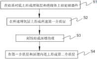
为实现本发明之又一目的,本发明提供一种绝缘体上硅射频器件的制造方法,所述方法包括:To achieve another object of the present invention, the present invention provides a method for manufacturing a silicon-on-insulator radio frequency device, the method comprising:
执行步骤S1:在所述硅基衬底上形成所述埋氧层和绝缘体上硅射频器件;Executing step S1: forming the buried oxide layer and a silicon-on-insulator radio frequency device on the silicon-based substrate;
执行步骤S2:在所述器件层之异于所述埋氧层的一侧设置第一介质层;Executing step S2: setting a first dielectric layer on the side of the device layer different from the buried oxide layer;
执行步骤S3:光刻、刻蚀所述埋氧层、器件层和第一介质层,并进行多晶硅填充、回刻,以形成所述深埋沟道;Executing step S3: photolithography, etching the buried oxide layer, the device layer and the first dielectric layer, and performing polysilicon filling and etching back to form the deep buried channel;
执行步骤S4:在所述第一介质层和所述深埋沟道之异于所述器件层的一侧设置第二介质层,获得所述绝缘体上硅射频器件。Executing step S4: setting a second dielectric layer on a side different from the device layer between the first dielectric layer and the deep-buried channel to obtain the silicon-on-insulator radio frequency device.
可选地,形成所述绝缘体上硅射频器件的步骤进一步包括,提供硅基衬底,所述硅基衬底用于支撑所述绝缘体上硅射频器件;在所述硅基衬底上设置埋氧层;在所述埋氧层之异于所述硅基衬底一侧设置器件层,所述器件层为硅层,所述器件层并具有器件区和用于器件隔离的浅沟槽隔离。Optionally, the step of forming the silicon-on-insulator radio frequency device further includes providing a silicon-based substrate for supporting the silicon-on-insulator radio frequency device; setting a buried Oxygen layer; a device layer is provided on the side of the buried oxide layer different from the silicon-based substrate, the device layer is a silicon layer, and the device layer has a device region and a shallow trench isolation for device isolation .
可选地,所述器件层的器件区设置p型阱、在所述p型阱两侧分别设置第一n型掺杂区和第二n型掺杂区,以及在所述p型阱之异于所述第一n型掺杂区和第二n型掺杂区的一侧设置所述多晶硅层。Optionally, a p-type well is set in the device region of the device layer, a first n-type doped region and a second n-type doped region are respectively set on both sides of the p-type well, and between the p-type well The polysilicon layer is provided on a side different from the first n-type doped region and the second n-type doped region.
可选地,形成所述深埋沟道的步骤进一步包括,光刻、刻蚀所述埋氧层、器件层和第一介质层,形成深埋沟道图案,所述深埋沟道图案贯穿设置于所述埋氧层、器件层和第一介质层,并介于所述器件层的浅沟槽隔离之间;在所述深埋沟道图案内进行多晶硅填充;对所述冗余的多晶硅进行回刻处理,以形成所述深埋沟道。Optionally, the step of forming the deep buried channel further includes photolithography, etching the buried oxide layer, the device layer and the first dielectric layer to form a deep buried channel pattern, and the deep buried channel pattern penetrates It is arranged on the buried oxide layer, the device layer and the first dielectric layer, and is between the shallow trench isolation of the device layer; polysilicon filling is performed in the deep buried channel pattern; the redundant The polysilicon is etched back to form the deep buried channel.
综上所述,本发明所述绝缘体上硅射频器件改善信号传输特性,避免了信号失真,且所述绝缘体上硅射频器件的制造方法简便,成本低,工艺局限性小。In summary, the silicon-on-insulator radio frequency device of the present invention improves signal transmission characteristics and avoids signal distortion, and the manufacturing method of the silicon-on-insulator radio frequency device is simple, low in cost, and has small process limitations.
附图说明Description of drawings
图1~图3所示为本发明具有不同结构的深埋沟道之绝缘体上硅射频器件的结构示意图;Fig. 1~Fig. 3 shows the structural representation of the silicon-on-insulator radio frequency device of the deep-buried channel with different structures of the present invention;
图4所示为本发明绝缘体上硅射频器件的制造方法流程图。Fig. 4 is a flowchart of a method for manufacturing a silicon-on-insulator radio frequency device according to the present invention.
图5~图8所示为本发明所述绝缘体上硅射频器件的制造分步结构示意图。5 to 8 are schematic diagrams showing the step-by-step manufacturing structure of the silicon-on-insulator radio frequency device of the present invention.
具体实施方式Detailed ways
为详细说明本发明创造的技术内容、构造特征、所达成目的及功效,下面将结合实施例并配合附图予以详细说明。In order to illustrate the technical content, structural features, achieved goals and effects of the present invention in detail, the following will be described in detail in conjunction with the embodiments and accompanying drawings.
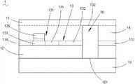
请参阅图1,图1所示为本发明绝缘体上硅射频器件的结构示意图。所述绝缘体上硅射频器件1包括硅基衬底11,所述硅基衬底11用于支撑所述绝缘体上硅射频器件1;埋氧层12,所述埋氧层12设置在所述硅基衬底11上;器件层13,所述器件层13为硅层,设置在所述埋氧层12之异于所述硅基衬底12一侧,所述器件层13并具有器件区131和用于器件隔离的浅沟槽隔离132;第一介质层14,所述第一介质层14覆盖所述器件层13;第二介质层15,所述第二介质层15设置在所述第一介质层14之异于所述器件层13一侧;以及深埋沟道16,所述深埋沟道16贯穿设置于所述埋氧层12、器件层13和第一介质层14,并介于所述器件层13的浅沟槽隔离132之间。Please refer to FIG. 1 . FIG. 1 is a schematic structural diagram of a silicon-on-insulator radio frequency device according to the present invention. The silicon-on-insulator radio frequency device 1 includes a silicon-based
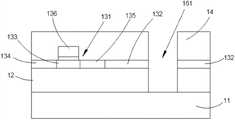
其中,所述器件层13的器件区131可设置p型阱133、在所述p型阱133两侧分别设置第一n型掺杂区134和第二n型掺杂区135,以及在所述p型阱133之异于所述第一n型掺杂区134和第二n型掺杂区135的一侧设置所述多晶硅层136。作为本发明的具体实施方式,所述深埋沟道16贯穿设置于所述埋氧层12、器件层13和第一介质层14,并介于所述器件层13的浅沟槽隔离132之间。具体地,所述深埋沟道16呈体状,并至所述硅基衬底11与所述埋氧层12之第一分界面101纵向延伸至所述第一介质层14与所述第二介质层15之第二分界面102。所述深埋沟道16的外向间距优选地为15~120μm。Wherein, the
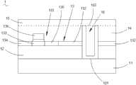
作为本领域的技术人员,不难理解地,所述深埋沟道16可以呈“凹”型,如图2所示。所述深埋沟道16也可呈间隔条状布置,如图3所示。所述深埋沟道16的外向间距优选地为15~120μm。As a person skilled in the art, it is not difficult to understand that the deep-buried
请参阅图4,并结合参阅5~图8,图4所示为本发明绝缘体上硅射频器件的制造方法流程图。图5~图8所示为本发明所述绝缘体上硅射频器件的制造分步结构示意图。在本实施例中,仅以所述深埋沟道16呈体状结构为例进行阐述,所述绝缘体上硅射频器件的制造方法,包括:Please refer to FIG. 4 , and refer to FIG. 5 to FIG. 8 in combination. FIG. 4 is a flow chart of a method for manufacturing a silicon-on-insulator radio frequency device according to the present invention. 5 to 8 are schematic diagrams showing the step-by-step manufacturing structure of the silicon-on-insulator radio frequency device of the present invention. In this embodiment, it is only described by taking the bulk structure of the deep-buried
执行步骤S1:在所述硅基衬底11上形成所述埋氧层12和所述绝缘体上硅射频器件1;Executing step S1: forming the buried
具体地,形成所述绝缘体上硅射频器件1的步骤进一步包括,Specifically, the step of forming the silicon-on-insulator radio frequency device 1 further includes,
一、提供硅基衬底11,所述硅基衬底11用于支撑所述绝缘体上硅射频器件1;1. Provide a silicon-based
二、在所述硅基衬底11上设置埋氧层12;2. Setting a buried
三、在所述埋氧层12之异于所述硅基衬底12一侧设置器件层13,所述器件层13为硅层,所述器件层13并具有器件区131和用于器件隔离的浅沟槽隔离132;3. A
其中,所述器件层13的器件区131可设置p型阱133、在所述p型阱133两侧分别设置第一n型掺杂区134和第二n型掺杂区135,以及在所述p型阱133之异于所述第一n型掺杂区134和第二n型掺杂区135的一侧设置所述多晶硅层136。Wherein, the
执行步骤S2:在所述器件层13之异于所述埋氧层12的一侧设置第一介质层14;Executing step S2: setting the first
执行步骤S3:光刻、刻蚀所述埋氧层12、器件层13和第一介质层14,并进行多晶硅17填充、回刻,以形成所述深埋沟道16;Executing step S3: photolithography, etching the buried
具体地,形成所述深埋沟道16的步骤进一步包括,Specifically, the step of forming the deep buried
一、光刻、刻蚀所述埋氧层12、器件层13和第一介质层14,形成深埋沟道图案161,所述深埋沟道图案161贯穿设置于所述埋氧层12、器件层13和第一介质层14,并介于所述器件层13的浅沟槽隔离132之间;1. Photolithography and etching the buried
二、在所述深埋沟道图案161内进行多晶硅17填充;2. Filling the deep buried
三、对所述冗余的多晶硅17进行回刻处理,以形成所述深埋沟道16。3. Etching back the
作为本发明的具体实施方式,所述深埋沟道16呈体状,贯穿设置于所述埋氧层12、器件层13和第一介质层14,并介于所述器件层13的浅沟槽隔离132之间。具体地,所述深埋沟道16至所述硅基衬底11与所述埋氧层12之第一分界面101纵向延伸至所述第一介质层14与所述第二介质层15之第二分界面102。所述深埋沟道16的外向间距优选地为15~120μm。As a specific embodiment of the present invention, the deep buried
执行步骤S4:在所述第一介质层14和所述深埋沟道16之异于所述器件层13的一侧设置第二介质层15,获得所述绝缘体上硅射频器件1。Executing step S4: disposing a
明显地,作为本领域的技术人员,不难理解地,所述深埋沟道16可以呈如图2所示的“凹”型,也可呈如图3所示的间隔条状布置。所述深埋沟道16的外向间距相应地优选为15~120μm。当所述深埋沟道16呈“凹”型,或呈间隔条状布置时,所述绝缘体上硅射频器件的制造方法仅在形成所述深埋沟道16时的光刻、刻蚀图案不同。为获得不同形状的深埋沟道16,本领域的技术人员结合传统工艺便可实现,在此不予赘述。类似地,所述深埋沟道16呈间隔条状布置时,所述条状结构数量包括但不限于图3所示的5个。Obviously, as a person skilled in the art, it is not difficult to understand that the deep-buried
综上所述,本发明所述绝缘体上硅射频器件改善信号传输特性,避免了信号失真,且所述绝缘体上硅射频器件的制造方法简便,成本低,工艺局限性小。In summary, the silicon-on-insulator radio frequency device of the present invention improves signal transmission characteristics and avoids signal distortion, and the manufacturing method of the silicon-on-insulator radio frequency device is simple, low in cost, and has small process limitations.
本领域技术人员均应了解,在不脱离本发明的精神或范围的情况下,可以对本发明进行各种修改和变型。因而,如果任何修改或变型落入所附权利要求书及等同物的保护范围内时,认为本发明涵盖这些修改和变型。Those skilled in the art will appreciate that various modifications and variations can be made in the present invention without departing from the spirit or scope of the invention. Therefore, if any modification or variation falls within the scope of protection of the appended claims and their equivalents, the present invention is deemed to cover such modification and variation.
Claims (11)
Translated fromChinesePriority Applications (2)
| Application Number | Priority Date | Filing Date | Title |
|---|---|---|---|
| CN2013100416370ACN103077950A (en) | 2013-02-01 | 2013-02-01 | Silicon radio frequency device on insulator and manufacturing method thereof |
| US14/142,200US9012996B2 (en) | 2013-02-01 | 2013-12-27 | Silicon-on-insulator radio-frequency device and method of forming the same |
Applications Claiming Priority (1)
| Application Number | Priority Date | Filing Date | Title |
|---|---|---|---|
| CN2013100416370ACN103077950A (en) | 2013-02-01 | 2013-02-01 | Silicon radio frequency device on insulator and manufacturing method thereof |
Publications (1)
| Publication Number | Publication Date |
|---|---|
| CN103077950Atrue CN103077950A (en) | 2013-05-01 |
Family
ID=48154431
Family Applications (1)
| Application Number | Title | Priority Date | Filing Date |
|---|---|---|---|
| CN2013100416370APendingCN103077950A (en) | 2013-02-01 | 2013-02-01 | Silicon radio frequency device on insulator and manufacturing method thereof |
Country Status (2)
| Country | Link |
|---|---|
| US (1) | US9012996B2 (en) |
| CN (1) | CN103077950A (en) |
Families Citing this family (4)
| Publication number | Priority date | Publication date | Assignee | Title |
|---|---|---|---|---|
| CN103077949B (en)* | 2013-01-28 | 2016-09-14 | 上海华虹宏力半导体制造有限公司 | Silicon radio frequency device on insulator and preparation method thereof |
| CN115332153A (en) | 2017-12-29 | 2022-11-11 | 联华电子股份有限公司 | Semiconductor element and manufacturing method thereof |
| CN110021559B (en) | 2018-01-09 | 2021-08-24 | 联华电子股份有限公司 | Semiconductor device and method of making the same |
| US11658223B2 (en) | 2020-10-19 | 2023-05-23 | United Microelectronics Corp. | Semiconductor structure |
Citations (4)
| Publication number | Priority date | Publication date | Assignee | Title |
|---|---|---|---|---|
| JPH08222710A (en)* | 1995-02-17 | 1996-08-30 | Mitsubishi Electric Corp | Semiconductor device |
| CN1705132A (en)* | 2004-05-27 | 2005-12-07 | 中国科学院微电子研究所 | Integrated structure of insulator silicon radio frequency integrated circuit and manufacturing method |
| CN101840935A (en)* | 2010-05-17 | 2010-09-22 | 电子科技大学 | SOI (Silicon-on-insulator) MOSFET lateral (metal-oxide-semiconductor field effect transistor) device |
| US20120038024A1 (en)* | 2010-08-10 | 2012-02-16 | International Business Machines Corporation | Low harmonic rf switch in soi |
Family Cites Families (1)
| Publication number | Priority date | Publication date | Assignee | Title |
|---|---|---|---|---|
| US6429477B1 (en)* | 2000-10-31 | 2002-08-06 | International Business Machines Corporation | Shared body and diffusion contact structure and method for fabricating same |
- 2013
- 2013-02-01CNCN2013100416370Apatent/CN103077950A/enactivePending
- 2013-12-27USUS14/142,200patent/US9012996B2/enactiveActive
Patent Citations (4)
| Publication number | Priority date | Publication date | Assignee | Title |
|---|---|---|---|---|
| JPH08222710A (en)* | 1995-02-17 | 1996-08-30 | Mitsubishi Electric Corp | Semiconductor device |
| CN1705132A (en)* | 2004-05-27 | 2005-12-07 | 中国科学院微电子研究所 | Integrated structure of insulator silicon radio frequency integrated circuit and manufacturing method |
| CN101840935A (en)* | 2010-05-17 | 2010-09-22 | 电子科技大学 | SOI (Silicon-on-insulator) MOSFET lateral (metal-oxide-semiconductor field effect transistor) device |
| US20120038024A1 (en)* | 2010-08-10 | 2012-02-16 | International Business Machines Corporation | Low harmonic rf switch in soi |
Also Published As
| Publication number | Publication date |
|---|---|
| US20140217503A1 (en) | 2014-08-07 |
| US9012996B2 (en) | 2015-04-21 |
Similar Documents
| Publication | Publication Date | Title |
|---|---|---|
| CN106409825B (en) | The semiconductor devices and radio-frequency module formed on High resistivity substrate | |
| US9543190B2 (en) | Method of fabricating semiconductor device having a trench structure penetrating a buried layer | |
| US9780164B2 (en) | Silicon-on-insulator radio frequency device and silicon-on-insulator substrate | |
| US9466729B1 (en) | Etch stop region based fabrication of bonded semiconductor structures | |
| CN113284806B (en) | Ring gate device, source-drain preparation method thereof, device preparation method and electronic equipment | |
| TW201842668A (en) | Heterojunction bipolar transistor with stress material for improved mobility | |
| CN109994491A (en) | HV Complementary Bipolar Transistor with Lateral Collector on SOI | |
| CN103077950A (en) | Silicon radio frequency device on insulator and manufacturing method thereof | |
| CN105161500A (en) | Insulator-on-silicon (SOI) radio-frequency device structure | |
| CN114464675A (en) | Composite gate IGBT device structure and preparation method thereof | |
| CN103441131A (en) | Partially-depleted silicon-on-insulator device structure | |
| CN104810334B (en) | Semiconductor device | |
| CN106257671A (en) | The semiconductor device formed on High resistivity substrate and radio-frequency module | |
| US9653344B2 (en) | Device isolation structure and manufacture method | |
| CN104362091B (en) | The manufacture method of double trench field-effect pipes | |
| US9171952B2 (en) | Low gate-to-drain capacitance fully merged finFET | |
| CN107316864B (en) | Transient Voltage Suppressor and preparation method thereof | |
| CN104658907B (en) | Manufacturing method of reverse-resistance type insulated gate bipolar transistor | |
| CN104347419B (en) | A kind of ESD protective device and preparation method thereof | |
| CN104167432B (en) | Radio-frequency LDMOS device edge isolation structure and manufacturing method | |
| CN105047720B (en) | Silicon-on-insulator RF switching devices structure | |
| CN104766889A (en) | Silicon-on-insulator RF switching device structure | |
| CN106876440A (en) | Reduce substrat structure of SOI substrate capacity effect and preparation method thereof | |
| JP6102823B2 (en) | Method for evaluating SOI substrate | |
| CN103413777A (en) | Deep groove filling structure and manufacturing method thereof |
Legal Events
| Date | Code | Title | Description |
|---|---|---|---|
| C06 | Publication | ||
| PB01 | Publication | ||
| ASS | Succession or assignment of patent right | Owner name:SHANGHAI HUAHONG GRACE SEMICONDUCTOR MANUFACTURING Free format text:FORMER OWNER: HONGLI SEMICONDUCTOR MANUFACTURE CO LTD, SHANGHAI Effective date:20140506 | |
| C41 | Transfer of patent application or patent right or utility model | ||
| TA01 | Transfer of patent application right | Effective date of registration:20140506 Address after:201203 Shanghai city Zuchongzhi road Pudong New Area Zhangjiang hi tech Park No. 1399 Applicant after:Shanghai Huahong Grace Semiconductor Manufacturing Corporation Address before:201203 Shanghai Guo Shou Jing Road, Pudong New Area Zhangjiang hi tech Park No. 818 Applicant before:Hongli Semiconductor Manufacture Co., Ltd., Shanghai | |
| C10 | Entry into substantive examination | ||
| SE01 | Entry into force of request for substantive examination | ||
| RJ01 | Rejection of invention patent application after publication | Application publication date:20130501 | |
| RJ01 | Rejection of invention patent application after publication |