CN103069502A - Etch patterning of nanostructure transparent conductors - Google Patents
Etch patterning of nanostructure transparent conductorsDownload PDFInfo
- Publication number
- CN103069502A CN103069502ACN2011800228101ACN201180022810ACN103069502ACN 103069502 ACN103069502 ACN 103069502ACN 2011800228101 ACN2011800228101 ACN 2011800228101ACN 201180022810 ACN201180022810 ACN 201180022810ACN 103069502 ACN103069502 ACN 103069502A
- Authority
- CN
- China
- Prior art keywords
- conductive
- nanowires
- resistivity
- acid
- etching
- Prior art date
- Legal status (The legal status is an assumption and is not a legal conclusion. Google has not performed a legal analysis and makes no representation as to the accuracy of the status listed.)
- Pending
Links
- 239000004020conductorSubstances0.000titleclaimsabstractdescription103
- 239000002086nanomaterialSubstances0.000titledescription36
- 238000000059patterningMethods0.000titledescription33
- 238000005530etchingMethods0.000claimsabstractdescription114
- 239000000203mixtureSubstances0.000claimsabstractdescription42
- 239000002253acidSubstances0.000claimsabstractdescription41
- 238000009472formulationMethods0.000claimsabstractdescription28
- 238000007650screen-printingMethods0.000claimsabstractdescription11
- 239000002070nanowireSubstances0.000claimsdescription150
- 238000000034methodMethods0.000claimsdescription86
- 229910052751metalInorganic materials0.000claimsdescription70
- 239000002184metalSubstances0.000claimsdescription70
- 229920000642polymerPolymers0.000claimsdescription38
- -1poly(2-acrylamido-2-methyl-1-propanesulfonic acid)Polymers0.000claimsdescription36
- XLYOFNOQVPJJNP-UHFFFAOYSA-NwaterSubstancesOXLYOFNOQVPJJNP-UHFFFAOYSA-N0.000claimsdescription35
- 238000002834transmittanceMethods0.000claimsdescription24
- GRYLNZFGIOXLOG-UHFFFAOYSA-NNitric acidChemical compoundO[N+]([O-])=OGRYLNZFGIOXLOG-UHFFFAOYSA-N0.000claimsdescription15
- 229910017604nitric acidInorganic materials0.000claimsdescription15
- 150000007513acidsChemical class0.000claimsdescription13
- ORTQZVOHEJQUHG-UHFFFAOYSA-Lcopper(II) chlorideChemical compoundCl[Cu]ClORTQZVOHEJQUHG-UHFFFAOYSA-L0.000claimsdescription13
- 239000012670alkaline solutionSubstances0.000claimsdescription12
- 229910021592Copper(II) chlorideInorganic materials0.000claimsdescription9
- NBIIXXVUZAFLBC-UHFFFAOYSA-NPhosphoric acidChemical compoundOP(O)(O)=ONBIIXXVUZAFLBC-UHFFFAOYSA-N0.000claimsdescription8
- 230000002378acidificating effectEffects0.000claimsdescription8
- 239000004952PolyamideSubstances0.000claimsdescription7
- RBTARNINKXHZNM-UHFFFAOYSA-Kiron trichlorideChemical groupCl[Fe](Cl)ClRBTARNINKXHZNM-UHFFFAOYSA-K0.000claimsdescription7
- 229920002647polyamidePolymers0.000claimsdescription7
- 229910021578Iron(III) chlorideInorganic materials0.000claimsdescription6
- 229910001507metal halideInorganic materials0.000claimsdescription6
- 150000005309metal halidesChemical class0.000claimsdescription6
- 238000000137annealingMethods0.000claimsdescription5
- 239000002798polar solventSubstances0.000claimsdescription5
- 229920001798poly[2-(acrylamido)-2-methyl-1-propanesulfonic acid] polymerPolymers0.000claimsdescription4
- 235000011007phosphoric acidNutrition0.000claims2
- 239000000853adhesiveSubstances0.000claims1
- 230000001070adhesive effectEffects0.000claims1
- 239000000758substrateSubstances0.000abstractdescription73
- 239000011159matrix materialSubstances0.000description97
- 239000010410layerSubstances0.000description86
- 239000010408filmSubstances0.000description85
- BQCADISMDOOEFD-UHFFFAOYSA-NSilverChemical compound[Ag]BQCADISMDOOEFD-UHFFFAOYSA-N0.000description55
- 239000002042Silver nanowireSubstances0.000description42
- 230000003287optical effectEffects0.000description39
- 239000000243solutionSubstances0.000description39
- 229920000139polyethylene terephthalatePolymers0.000description36
- 239000005020polyethylene terephthalateSubstances0.000description36
- HEMHJVSKTPXQMS-UHFFFAOYSA-MSodium hydroxideChemical compound[OH-].[Na+]HEMHJVSKTPXQMS-UHFFFAOYSA-M0.000description27
- 238000010438heat treatmentMethods0.000description26
- VEXZGXHMUGYJMC-UHFFFAOYSA-NHydrochloric acidChemical compoundClVEXZGXHMUGYJMC-UHFFFAOYSA-N0.000description22
- 230000008569processEffects0.000description22
- 230000005540biological transmissionEffects0.000description19
- 239000001866hydroxypropyl methyl celluloseSubstances0.000description18
- 229920003088hydroxypropyl methyl cellulosePolymers0.000description18
- UFVKGYZPFZQRLF-UHFFFAOYSA-Nhydroxypropyl methyl celluloseChemical compoundOC1C(O)C(OC)OC(CO)C1OC1C(O)C(O)C(OC2C(C(O)C(OC3C(C(O)C(O)C(CO)O3)O)C(CO)O2)O)C(CO)O1UFVKGYZPFZQRLF-UHFFFAOYSA-N0.000description18
- 235000010979hydroxypropyl methyl celluloseNutrition0.000description18
- 239000011241protective layerSubstances0.000description17
- 239000002904solventSubstances0.000description17
- 239000006185dispersionSubstances0.000description15
- 239000000976inkSubstances0.000description15
- 239000002245particleSubstances0.000description15
- 230000008859changeEffects0.000description14
- 238000000151depositionMethods0.000description14
- 239000000463materialSubstances0.000description14
- 229920002120photoresistant polymerPolymers0.000description14
- 239000007800oxidant agentSubstances0.000description13
- 239000004814polyurethaneSubstances0.000description13
- 229910052709silverInorganic materials0.000description13
- 239000004332silverSubstances0.000description13
- WEVYAHXRMPXWCK-UHFFFAOYSA-NAcetonitrileChemical compoundCC#NWEVYAHXRMPXWCK-UHFFFAOYSA-N0.000description12
- 230000036961partial effectEffects0.000description12
- 239000004094surface-active agentSubstances0.000description12
- 230000001965increasing effectEffects0.000description11
- 229910044991metal oxideInorganic materials0.000description11
- 150000004706metal oxidesChemical class0.000description11
- 229920002635polyurethanePolymers0.000description11
- QTBSBXVTEAMEQO-UHFFFAOYSA-NAcetic acidChemical compoundCC(O)=OQTBSBXVTEAMEQO-UHFFFAOYSA-N0.000description10
- 239000011521glassSubstances0.000description10
- 239000012286potassium permanganateSubstances0.000description10
- ZWEHNKRNPOVVGH-UHFFFAOYSA-N2-ButanoneChemical compoundCCC(C)=OZWEHNKRNPOVVGH-UHFFFAOYSA-N0.000description9
- 239000007788liquidSubstances0.000description9
- 238000006116polymerization reactionMethods0.000description9
- 230000002829reductive effectEffects0.000description9
- 238000012360testing methodMethods0.000description9
- 239000011248coating agentSubstances0.000description8
- 238000000576coating methodMethods0.000description8
- 230000008021depositionEffects0.000description8
- 238000011068loading methodMethods0.000description8
- 239000012528membraneSubstances0.000description8
- 239000000178monomerSubstances0.000description8
- 239000004417polycarbonateSubstances0.000description8
- 229920000515polycarbonatePolymers0.000description8
- MHAJPDPJQMAIIY-UHFFFAOYSA-NHydrogen peroxideChemical compoundOOMHAJPDPJQMAIIY-UHFFFAOYSA-N0.000description7
- 150000003839saltsChemical class0.000description7
- UHOVQNZJYSORNB-UHFFFAOYSA-NBenzeneChemical compoundC1=CC=CC=C1UHOVQNZJYSORNB-UHFFFAOYSA-N0.000description6
- LYCAIKOWRPUZTN-UHFFFAOYSA-NEthylene glycolChemical compoundOCCOLYCAIKOWRPUZTN-UHFFFAOYSA-N0.000description6
- 239000004372Polyvinyl alcoholSubstances0.000description6
- YXFVVABEGXRONW-UHFFFAOYSA-NTolueneChemical compoundCC1=CC=CC=C1YXFVVABEGXRONW-UHFFFAOYSA-N0.000description6
- ZMANZCXQSJIPKH-UHFFFAOYSA-NTriethylamineChemical compoundCCN(CC)CCZMANZCXQSJIPKH-UHFFFAOYSA-N0.000description6
- QVGXLLKOCUKJST-UHFFFAOYSA-Natomic oxygenChemical compound[O]QVGXLLKOCUKJST-UHFFFAOYSA-N0.000description6
- 235000019447hydroxyethyl celluloseNutrition0.000description6
- 229920000609methyl cellulosePolymers0.000description6
- 239000001923methylcelluloseSubstances0.000description6
- 235000010981methylcelluloseNutrition0.000description6
- 229910052760oxygenInorganic materials0.000description6
- 239000001301oxygenSubstances0.000description6
- 229920000058polyacrylatePolymers0.000description6
- 229920000098polyolefinPolymers0.000description6
- 229920002451polyvinyl alcoholPolymers0.000description6
- 235000019422polyvinyl alcoholNutrition0.000description6
- 238000002360preparation methodMethods0.000description6
- 239000007787solidSubstances0.000description6
- 239000004034viscosity adjusting agentSubstances0.000description6
- CBENFWSGALASAD-UHFFFAOYSA-NOzoneChemical compound[O-][O+]=OCBENFWSGALASAD-UHFFFAOYSA-N0.000description5
- KDLHZDBZIXYQEI-UHFFFAOYSA-NPalladiumChemical compound[Pd]KDLHZDBZIXYQEI-UHFFFAOYSA-N0.000description5
- 239000004642PolyimideSubstances0.000description5
- 239000000654additiveSubstances0.000description5
- 239000011230binding agentSubstances0.000description5
- 229920001940conductive polymerPolymers0.000description5
- 229920001577copolymerPolymers0.000description5
- 230000001590oxidative effectEffects0.000description5
- 229920000647polyepoxidePolymers0.000description5
- 229920001721polyimidePolymers0.000description5
- 229920001296polysiloxanePolymers0.000description5
- 239000000126substanceSubstances0.000description5
- CWSZBVAUYPTXTG-UHFFFAOYSA-N5-[6-[[3,4-dihydroxy-6-(hydroxymethyl)-5-methoxyoxan-2-yl]oxymethyl]-3,4-dihydroxy-5-[4-hydroxy-3-(2-hydroxyethoxy)-6-(hydroxymethyl)-5-methoxyoxan-2-yl]oxyoxan-2-yl]oxy-6-(hydroxymethyl)-2-methyloxane-3,4-diolChemical compoundO1C(CO)C(OC)C(O)C(O)C1OCC1C(OC2C(C(O)C(OC)C(CO)O2)OCCO)C(O)C(O)C(OC2C(OC(C)C(O)C2O)CO)O1CWSZBVAUYPTXTG-UHFFFAOYSA-N0.000description4
- 229920002134Carboxymethyl cellulosePolymers0.000description4
- 229920000663Hydroxyethyl cellulosePolymers0.000description4
- KFZMGEQAYNKOFK-UHFFFAOYSA-NIsopropanolChemical compoundCC(C)OKFZMGEQAYNKOFK-UHFFFAOYSA-N0.000description4
- PXHVJJICTQNCMI-UHFFFAOYSA-NNickelChemical compound[Ni]PXHVJJICTQNCMI-UHFFFAOYSA-N0.000description4
- 239000004793PolystyreneSubstances0.000description4
- KWYUFKZDYYNOTN-UHFFFAOYSA-MPotassium hydroxideChemical compound[OH-].[K+]KWYUFKZDYYNOTN-UHFFFAOYSA-M0.000description4
- XECAHXYUAAWDEL-UHFFFAOYSA-Nacrylonitrile butadiene styreneChemical compoundC=CC=C.C=CC#N.C=CC1=CC=CC=C1XECAHXYUAAWDEL-UHFFFAOYSA-N0.000description4
- 239000004676acrylonitrile butadiene styreneSubstances0.000description4
- 229920000122acrylonitrile butadiene styrenePolymers0.000description4
- 229910052799carbonInorganic materials0.000description4
- 229920002678cellulosePolymers0.000description4
- 229920002313fluoropolymerPolymers0.000description4
- 229930195733hydrocarbonNatural products0.000description4
- WQYVRQLZKVEZGA-UHFFFAOYSA-NhypochloriteChemical compoundCl[O-]WQYVRQLZKVEZGA-UHFFFAOYSA-N0.000description4
- 229910001510metal chlorideInorganic materials0.000description4
- 239000002105nanoparticleSubstances0.000description4
- 238000005325percolationMethods0.000description4
- 229920003207poly(ethylene-2,6-naphthalate)Polymers0.000description4
- 229920002492poly(sulfone)Polymers0.000description4
- 229920000728polyesterPolymers0.000description4
- 239000011112polyethylene naphthalateSubstances0.000description4
- 229920002223polystyrenePolymers0.000description4
- 239000004800polyvinyl chlorideSubstances0.000description4
- 238000007639printingMethods0.000description4
- SQGYOTSLMSWVJD-UHFFFAOYSA-Nsilver(1+) nitrateChemical compound[Ag+].[O-]N(=O)=OSQGYOTSLMSWVJD-UHFFFAOYSA-N0.000description4
- 238000004528spin coatingMethods0.000description4
- 239000000725suspensionSubstances0.000description4
- WGTYBPLFGIVFAS-UHFFFAOYSA-Mtetramethylammonium hydroxideChemical compound[OH-].C[N+](C)(C)CWGTYBPLFGIVFAS-UHFFFAOYSA-M0.000description4
- 239000000230xanthan gumSubstances0.000description4
- 229920001285xanthan gumPolymers0.000description4
- 235000010493xanthan gumNutrition0.000description4
- 229940082509xanthan gumDrugs0.000description4
- 229910018072Al 2 O 3Inorganic materials0.000description3
- NLZUEZXRPGMBCV-UHFFFAOYSA-NButylhydroxytolueneChemical compoundCC1=CC(C(C)(C)C)=C(O)C(C(C)(C)C)=C1NLZUEZXRPGMBCV-UHFFFAOYSA-N0.000description3
- RYGMFSIKBFXOCR-UHFFFAOYSA-NCopperChemical compound[Cu]RYGMFSIKBFXOCR-UHFFFAOYSA-N0.000description3
- 229910021591Copper(I) chlorideInorganic materials0.000description3
- 229920000265PolyparaphenylenePolymers0.000description3
- 229910004298SiO 2Inorganic materials0.000description3
- 229910021607Silver chlorideInorganic materials0.000description3
- 229910000147aluminium phosphateInorganic materials0.000description3
- 239000010949copperSubstances0.000description3
- 229910052802copperInorganic materials0.000description3
- OXBLHERUFWYNTN-UHFFFAOYSA-Mcopper(I) chlorideChemical compound[Cu]ClOXBLHERUFWYNTN-UHFFFAOYSA-M0.000description3
- 238000009792diffusion processMethods0.000description3
- 239000003822epoxy resinSubstances0.000description3
- 235000019441ethanolNutrition0.000description3
- 238000001704evaporationMethods0.000description3
- 230000008020evaporationEffects0.000description3
- 238000002474experimental methodMethods0.000description3
- 239000012530fluidSubstances0.000description3
- 150000004820halidesChemical class0.000description3
- 238000004519manufacturing processMethods0.000description3
- 238000005259measurementMethods0.000description3
- 229910001092metal group alloyInorganic materials0.000description3
- 150000002739metalsChemical class0.000description3
- HKZLPVFGJNLROG-UHFFFAOYSA-Msilver monochlorideChemical compound[Cl-].[Ag+]HKZLPVFGJNLROG-UHFFFAOYSA-M0.000description3
- 239000010409thin filmSubstances0.000description3
- GPRLSGONYQIRFK-MNYXATJNSA-NtritonChemical compound[3H+]GPRLSGONYQIRFK-MNYXATJNSA-N0.000description3
- 229920002554vinyl polymerPolymers0.000description3
- ARXJGSRGQADJSQ-UHFFFAOYSA-N1-methoxypropan-2-olChemical compoundCOCC(C)OARXJGSRGQADJSQ-UHFFFAOYSA-N0.000description2
- LCZVSXRMYJUNFX-UHFFFAOYSA-N2-[2-(2-hydroxypropoxy)propoxy]propan-1-olChemical compoundCC(O)COC(C)COC(C)COLCZVSXRMYJUNFX-UHFFFAOYSA-N0.000description2
- ZRYCRPNCXLQHPN-UHFFFAOYSA-N3-hydroxy-2-methylbenzaldehydeChemical compoundCC1=C(O)C=CC=C1C=OZRYCRPNCXLQHPN-UHFFFAOYSA-N0.000description2
- CSCPPACGZOOCGX-UHFFFAOYSA-NAcetoneChemical compoundCC(C)=OCSCPPACGZOOCGX-UHFFFAOYSA-N0.000description2
- VHUUQVKOLVNVRT-UHFFFAOYSA-NAmmonium hydroxideChemical compound[NH4+].[OH-]VHUUQVKOLVNVRT-UHFFFAOYSA-N0.000description2
- IJGRMHOSHXDMSA-UHFFFAOYSA-NAtomic nitrogenChemical compoundN#NIJGRMHOSHXDMSA-UHFFFAOYSA-N0.000description2
- 239000004215Carbon black (E152)Substances0.000description2
- 229920002284Cellulose triacetatePolymers0.000description2
- 239000004971Cross linkerSubstances0.000description2
- 229920002943EPDM rubberPolymers0.000description2
- 206010073306Exposure to radiationDiseases0.000description2
- 239000004354Hydroxyethyl celluloseSubstances0.000description2
- CTQNGGLPUBDAKN-UHFFFAOYSA-NO-XyleneChemical compoundCC1=CC=CC=C1CCTQNGGLPUBDAKN-UHFFFAOYSA-N0.000description2
- 239000002033PVDF binderSubstances0.000description2
- 229920001609Poly(3,4-ethylenedioxythiophene)Polymers0.000description2
- 239000004962Polyamide-imideSubstances0.000description2
- 239000004695Polyether sulfoneSubstances0.000description2
- 239000004697PolyetherimideSubstances0.000description2
- 239000004698PolyethyleneSubstances0.000description2
- 239000004743PolypropyleneSubstances0.000description2
- 229920001328Polyvinylidene chloridePolymers0.000description2
- VYPSYNLAJGMNEJ-UHFFFAOYSA-NSilicium dioxideChemical compoundO=[Si]=OVYPSYNLAJGMNEJ-UHFFFAOYSA-N0.000description2
- WYURNTSHIVDZCO-UHFFFAOYSA-NTetrahydrofuranChemical compoundC1CCOC1WYURNTSHIVDZCO-UHFFFAOYSA-N0.000description2
- NNLVGZFZQQXQNW-ADJNRHBOSA-N[(2r,3r,4s,5r,6s)-4,5-diacetyloxy-3-[(2s,3r,4s,5r,6r)-3,4,5-triacetyloxy-6-(acetyloxymethyl)oxan-2-yl]oxy-6-[(2r,3r,4s,5r,6s)-4,5,6-triacetyloxy-2-(acetyloxymethyl)oxan-3-yl]oxyoxan-2-yl]methyl acetateChemical compoundO([C@@H]1O[C@@H]([C@H]([C@H](OC(C)=O)[C@H]1OC(C)=O)O[C@H]1[C@@H]([C@@H](OC(C)=O)[C@H](OC(C)=O)[C@@H](COC(C)=O)O1)OC(C)=O)COC(=O)C)[C@@H]1[C@@H](COC(C)=O)O[C@@H](OC(C)=O)[C@H](OC(C)=O)[C@H]1OC(C)=ONNLVGZFZQQXQNW-ADJNRHBOSA-N0.000description2
- 238000005299abrasionMethods0.000description2
- 238000010521absorption reactionMethods0.000description2
- DHKHKXVYLBGOIT-UHFFFAOYSA-Nacetaldehyde Diethyl AcetalNatural productsCCOC(C)OCCDHKHKXVYLBGOIT-UHFFFAOYSA-N0.000description2
- 150000001241acetalsChemical class0.000description2
- 150000001252acrylic acid derivativesChemical class0.000description2
- NIXOWILDQLNWCW-UHFFFAOYSA-Nacrylic acid groupChemical groupC(C=C)(=O)ONIXOWILDQLNWCW-UHFFFAOYSA-N0.000description2
- 150000001298alcoholsChemical class0.000description2
- 239000003513alkaliSubstances0.000description2
- 229910052782aluminiumInorganic materials0.000description2
- XAGFODPZIPBFFR-UHFFFAOYSA-NaluminiumChemical compound[Al]XAGFODPZIPBFFR-UHFFFAOYSA-N0.000description2
- 235000011114ammonium hydroxideNutrition0.000description2
- ROOXNKNUYICQNP-UHFFFAOYSA-Nammonium persulfateChemical compound[NH4+].[NH4+].[O-]S(=O)(=O)OOS([O-])(=O)=OROOXNKNUYICQNP-UHFFFAOYSA-N0.000description2
- 150000001450anionsChemical class0.000description2
- 238000013459approachMethods0.000description2
- 239000003849aromatic solventSubstances0.000description2
- 239000002585baseSubstances0.000description2
- 230000009286beneficial effectEffects0.000description2
- 230000015572biosynthetic processEffects0.000description2
- 230000000903blocking effectEffects0.000description2
- 238000009835boilingMethods0.000description2
- 239000002041carbon nanotubeSubstances0.000description2
- 239000001768carboxy methyl celluloseSubstances0.000description2
- 235000010948carboxy methyl celluloseNutrition0.000description2
- 239000008112carboxymethyl-celluloseSubstances0.000description2
- 239000001913celluloseSubstances0.000description2
- 229920002301cellulose acetatePolymers0.000description2
- 238000006243chemical reactionMethods0.000description2
- 150000001875compoundsChemical class0.000description2
- 230000001276controlling effectEffects0.000description2
- 238000005260corrosionMethods0.000description2
- 230000007797corrosionEffects0.000description2
- 125000004122cyclic groupChemical group0.000description2
- 150000001925cycloalkenesChemical class0.000description2
- 230000003247decreasing effectEffects0.000description2
- 239000008367deionised waterSubstances0.000description2
- 229910021641deionized waterInorganic materials0.000description2
- 230000001419dependent effectEffects0.000description2
- 238000007598dipping methodMethods0.000description2
- 238000004090dissolutionMethods0.000description2
- 238000001035dryingMethods0.000description2
- 230000000694effectsEffects0.000description2
- 239000012777electrically insulating materialSubstances0.000description2
- 238000005516engineering processMethods0.000description2
- 230000007613environmental effectEffects0.000description2
- 239000004811fluoropolymerSubstances0.000description2
- PCHJSUWPFVWCPO-UHFFFAOYSA-NgoldChemical compound[Au]PCHJSUWPFVWCPO-UHFFFAOYSA-N0.000description2
- 229910052737goldInorganic materials0.000description2
- 239000010931goldSubstances0.000description2
- 238000007756gravure coatingMethods0.000description2
- 229910052736halogenInorganic materials0.000description2
- 150000002367halogensChemical class0.000description2
- 150000002430hydrocarbonsChemical class0.000description2
- 229910052739hydrogenInorganic materials0.000description2
- 150000002576ketonesChemical class0.000description2
- 238000003475laminationMethods0.000description2
- 239000004973liquid crystal related substanceSubstances0.000description2
- 230000008018meltingEffects0.000description2
- 238000002844meltingMethods0.000description2
- 150000002736metal compoundsChemical class0.000description2
- 239000007769metal materialSubstances0.000description2
- 238000002156mixingMethods0.000description2
- 239000002071nanotubeSubstances0.000description2
- 229910052759nickelInorganic materials0.000description2
- 239000012299nitrogen atmosphereSubstances0.000description2
- 230000009972noncorrosive effectEffects0.000description2
- 150000007530organic basesChemical class0.000description2
- 230000003647oxidationEffects0.000description2
- 238000007254oxidation reactionMethods0.000description2
- 229910052763palladiumInorganic materials0.000description2
- 229920001568phenolic resinPolymers0.000description2
- 239000005011phenolic resinSubstances0.000description2
- 238000000206photolithographyMethods0.000description2
- 238000009832plasma treatmentMethods0.000description2
- BASFCYQUMIYNBI-UHFFFAOYSA-NplatinumChemical compound[Pt]BASFCYQUMIYNBI-UHFFFAOYSA-N0.000description2
- 229920000636poly(norbornene) polymerPolymers0.000description2
- 229920000548poly(silane) polymerPolymers0.000description2
- 229920002239polyacrylonitrilePolymers0.000description2
- 229920002312polyamide-imidePolymers0.000description2
- 229920006393polyether sulfonePolymers0.000description2
- 229920001601polyetherimidePolymers0.000description2
- 229920000573polyethylenePolymers0.000description2
- 229920005597polymer membranePolymers0.000description2
- 229920000193polymethacrylatePolymers0.000description2
- 229920000306polymethylpentenePolymers0.000description2
- 239000011116polymethylpenteneSubstances0.000description2
- 229920005862polyolPolymers0.000description2
- 150000003077polyolsChemical class0.000description2
- 229920001155polypropylenePolymers0.000description2
- 229920000734polysilsesquioxane polymerPolymers0.000description2
- 239000005077polysulfideSubstances0.000description2
- 229920001021polysulfidePolymers0.000description2
- 150000008117polysulfidesPolymers0.000description2
- 229920001343polytetrafluoroethylenePolymers0.000description2
- 239000004810polytetrafluoroethyleneSubstances0.000description2
- 229920000915polyvinyl chloridePolymers0.000description2
- 229920002102polyvinyl toluenePolymers0.000description2
- 239000005033polyvinylidene chlorideSubstances0.000description2
- 229920002981polyvinylidene fluoridePolymers0.000description2
- 238000012805post-processingMethods0.000description2
- 239000000843powderSubstances0.000description2
- 238000012545processingMethods0.000description2
- 239000000047productSubstances0.000description2
- 229920005573silicon-containing polymerPolymers0.000description2
- 150000003378silverChemical class0.000description2
- 229910001961silver nitrateInorganic materials0.000description2
- AYKOTYRPPUMHMT-UHFFFAOYSA-Nsilver;hydrateChemical compoundO.[Ag]AYKOTYRPPUMHMT-UHFFFAOYSA-N0.000description2
- VWDWKYIASSYTQR-UHFFFAOYSA-Nsodium nitrateChemical compound[Na+].[O-][N+]([O-])=OVWDWKYIASSYTQR-UHFFFAOYSA-N0.000description2
- 239000007921spraySubstances0.000description2
- 230000003746surface roughnessEffects0.000description2
- 229920003051synthetic elastomerPolymers0.000description2
- 239000005061synthetic rubberSubstances0.000description2
- 238000001771vacuum depositionMethods0.000description2
- 238000009736wettingMethods0.000description2
- 239000008096xyleneSubstances0.000description2
- NIXOWILDQLNWCW-UHFFFAOYSA-MAcrylateChemical compound[O-]C(=O)C=CNIXOWILDQLNWCW-UHFFFAOYSA-M0.000description1
- WKBOTKDWSSQWDR-UHFFFAOYSA-NBromine atomChemical compound[Br]WKBOTKDWSSQWDR-UHFFFAOYSA-N0.000description1
- OKTJSMMVPCPJKN-UHFFFAOYSA-NCarbonChemical compound[C]OKTJSMMVPCPJKN-UHFFFAOYSA-N0.000description1
- VEXZGXHMUGYJMC-UHFFFAOYSA-MChloride anionChemical compound[Cl-]VEXZGXHMUGYJMC-UHFFFAOYSA-M0.000description1
- XDTMQSROBMDMFD-UHFFFAOYSA-NCyclohexaneChemical compoundC1CCCCC1XDTMQSROBMDMFD-UHFFFAOYSA-N0.000description1
- 208000036829Device dislocationDiseases0.000description1
- 239000004593EpoxySubstances0.000description1
- LFQSCWFLJHTTHZ-UHFFFAOYSA-NEthanolChemical compoundCCOLFQSCWFLJHTTHZ-UHFFFAOYSA-N0.000description1
- IAYPIBMASNFSPL-UHFFFAOYSA-NEthylene oxideChemical compoundC1CO1IAYPIBMASNFSPL-UHFFFAOYSA-N0.000description1
- 229910004373HOAcInorganic materials0.000description1
- DGAQECJNVWCQMB-PUAWFVPOSA-MIlexoside XXIXChemical compoundC[C@@H]1CC[C@@]2(CC[C@@]3(C(=CC[C@H]4[C@]3(CC[C@@H]5[C@@]4(CC[C@@H](C5(C)C)OS(=O)(=O)[O-])C)C)[C@@H]2[C@]1(C)O)C)C(=O)O[C@H]6[C@@H]([C@H]([C@@H]([C@H](O6)CO)O)O)O.[Na+]DGAQECJNVWCQMB-PUAWFVPOSA-M0.000description1
- 229910018068Li 2 OInorganic materials0.000description1
- WHNWPMSKXPGLAX-UHFFFAOYSA-NN-Vinyl-2-pyrrolidoneChemical compoundC=CN1CCCC1=OWHNWPMSKXPGLAX-UHFFFAOYSA-N0.000description1
- 241000935974Paralichthys dentatusSpecies0.000description1
- GOOHAUXETOMSMM-UHFFFAOYSA-NPropylene oxideChemical compoundCC1CO1GOOHAUXETOMSMM-UHFFFAOYSA-N0.000description1
- QAOWNCQODCNURD-UHFFFAOYSA-LSulfateChemical compound[O-]S([O-])(=O)=OQAOWNCQODCNURD-UHFFFAOYSA-L0.000description1
- ULUAUXLGCMPNKK-UHFFFAOYSA-NSulfobutanedioic acidChemical classOC(=O)CC(C(O)=O)S(O)(=O)=OULUAUXLGCMPNKK-UHFFFAOYSA-N0.000description1
- NINIDFKCEFEMDL-UHFFFAOYSA-NSulfurChemical compound[S]NINIDFKCEFEMDL-UHFFFAOYSA-N0.000description1
- 239000012963UV stabilizerSubstances0.000description1
- 230000003213activating effectEffects0.000description1
- 239000012790adhesive layerSubstances0.000description1
- 230000002411adverseEffects0.000description1
- 238000005054agglomerationMethods0.000description1
- 230000002776aggregationEffects0.000description1
- 150000008044alkali metal hydroxidesChemical class0.000description1
- PNEYBMLMFCGWSK-UHFFFAOYSA-Naluminium oxideInorganic materials[O-2].[O-2].[O-2].[Al+3].[Al+3]PNEYBMLMFCGWSK-UHFFFAOYSA-N0.000description1
- 150000001412aminesChemical group0.000description1
- 239000000908ammonium hydroxideSubstances0.000description1
- 229910001870ammonium persulfateInorganic materials0.000description1
- 239000003963antioxidant agentSubstances0.000description1
- 239000007864aqueous solutionSubstances0.000description1
- 238000000149argon plasma sinteringMethods0.000description1
- 125000003118aryl groupChemical group0.000description1
- 230000008901benefitEffects0.000description1
- 239000007844bleaching agentSubstances0.000description1
- GDTBXPJZTBHREO-UHFFFAOYSA-NbromineSubstancesBrBrGDTBXPJZTBHREO-UHFFFAOYSA-N0.000description1
- 229910052794bromiumInorganic materials0.000description1
- 238000003486chemical etchingMethods0.000description1
- 150000003841chloride saltsChemical class0.000description1
- 150000001805chlorine compoundsChemical group0.000description1
- 239000010941cobaltSubstances0.000description1
- 229910017052cobaltInorganic materials0.000description1
- GUTLYIVDDKVIGB-UHFFFAOYSA-Ncobalt atomChemical compound[Co]GUTLYIVDDKVIGB-UHFFFAOYSA-N0.000description1
- 230000001010compromised effectEffects0.000description1
- 239000002322conducting polymerSubstances0.000description1
- 238000004132cross linkingMethods0.000description1
- 229960003280cupric chlorideDrugs0.000description1
- 238000007766curtain coatingMethods0.000description1
- 238000010586diagramMethods0.000description1
- KZHJGOXRZJKJNY-UHFFFAOYSA-Ndioxosilane;oxo(oxoalumanyloxy)alumaneChemical compoundO=[Si]=O.O=[Si]=O.O=[Al]O[Al]=O.O=[Al]O[Al]=O.O=[Al]O[Al]=OKZHJGOXRZJKJNY-UHFFFAOYSA-N0.000description1
- 238000003618dip coatingMethods0.000description1
- 238000009826distributionMethods0.000description1
- NLEBIOOXCVAHBD-QKMCSOCLSA-Ndodecyl beta-D-maltosideChemical compoundO[C@@H]1[C@@H](O)[C@H](OCCCCCCCCCCCC)O[C@H](CO)[C@H]1O[C@@H]1[C@H](O)[C@@H](O)[C@H](O)[C@@H](CO)O1NLEBIOOXCVAHBD-QKMCSOCLSA-N0.000description1
- 238000010894electron beam technologyMethods0.000description1
- 238000005370electroosmosisMethods0.000description1
- 230000002708enhancing effectEffects0.000description1
- 125000003700epoxy groupChemical group0.000description1
- 150000002170ethersChemical class0.000description1
- 230000001747exhibiting effectEffects0.000description1
- 239000004744fabricSubstances0.000description1
- 239000000835fiberSubstances0.000description1
- 230000004313glareEffects0.000description1
- 239000002241glass-ceramicSubstances0.000description1
- LNEPOXFFQSENCJ-UHFFFAOYSA-NhaloperidolChemical compoundC1CC(O)(C=2C=CC(Cl)=CC=2)CCN1CCCC(=O)C1=CC=C(F)C=C1LNEPOXFFQSENCJ-UHFFFAOYSA-N0.000description1
- XMBWDFGMSWQBCA-UHFFFAOYSA-Nhydrogen iodideChemical compoundIXMBWDFGMSWQBCA-UHFFFAOYSA-N0.000description1
- 238000011065in-situ storageMethods0.000description1
- AMGQUBHHOARCQH-UHFFFAOYSA-Nindium;oxotinChemical compound[In].[Sn]=OAMGQUBHHOARCQH-UHFFFAOYSA-N0.000description1
- 239000004615ingredientSubstances0.000description1
- 239000003112inhibitorSubstances0.000description1
- 230000000977initiatory effectEffects0.000description1
- 229910010272inorganic materialInorganic materials0.000description1
- 239000011147inorganic materialSubstances0.000description1
- 239000012212insulatorSubstances0.000description1
- 230000003993interactionEffects0.000description1
- PNDPGZBMCMUPRI-UHFFFAOYSA-NiodineChemical compoundIIPNDPGZBMCMUPRI-UHFFFAOYSA-N0.000description1
- 230000001678irradiating effectEffects0.000description1
- 238000002955isolationMethods0.000description1
- 230000000670limiting effectEffects0.000description1
- 230000007774longtermEffects0.000description1
- WPBNNNQJVZRUHP-UHFFFAOYSA-Lmanganese(2+);methyl n-[[2-(methoxycarbonylcarbamothioylamino)phenyl]carbamothioyl]carbamate;n-[2-(sulfidocarbothioylamino)ethyl]carbamodithioateChemical compound[Mn+2].[S-]C(=S)NCCNC([S-])=S.COC(=O)NC(=S)NC1=CC=CC=C1NC(=S)NC(=O)OCWPBNNNQJVZRUHP-UHFFFAOYSA-L0.000description1
- 229910021645metal ionInorganic materials0.000description1
- 238000012986modificationMethods0.000description1
- 230000004048modificationEffects0.000description1
- 229910003465moissaniteInorganic materials0.000description1
- 229910052863mulliteInorganic materials0.000description1
- 239000002120nanofilmSubstances0.000description1
- 239000002073nanorodSubstances0.000description1
- 229910052757nitrogenInorganic materials0.000description1
- 229920003986novolacPolymers0.000description1
- NRNFFDZCBYOZJY-UHFFFAOYSA-Np-quinodimethaneChemical compoundC=C1C=CC(=C)C=C1NRNFFDZCBYOZJY-UHFFFAOYSA-N0.000description1
- 238000012856packingMethods0.000description1
- 230000035515penetrationEffects0.000description1
- 150000002978peroxidesChemical class0.000description1
- 125000000864peroxy groupChemical groupO(O*)*0.000description1
- JRKICGRDRMAZLK-UHFFFAOYSA-Lpersulfate groupChemical groupS(=O)(=O)([O-])OOS(=O)(=O)[O-]JRKICGRDRMAZLK-UHFFFAOYSA-L0.000description1
- 238000005554picklingMethods0.000description1
- 229920003023plasticPolymers0.000description1
- 239000004033plasticSubstances0.000description1
- 239000002985plastic filmSubstances0.000description1
- 229920006255plastic filmPolymers0.000description1
- 229910052697platinumInorganic materials0.000description1
- 229920003229poly(methyl methacrylate)Polymers0.000description1
- 229920000767polyanilinePolymers0.000description1
- 229920000015polydiacetylenePolymers0.000description1
- 229920006254polymer filmPolymers0.000description1
- 239000003505polymerization initiatorSubstances0.000description1
- 229920013636polyphenyl ether polymerPolymers0.000description1
- 229920001955polyphenylene etherPolymers0.000description1
- 229920000123polythiophenePolymers0.000description1
- 229920000036polyvinylpyrrolidonePolymers0.000description1
- 239000001267polyvinylpyrrolidoneSubstances0.000description1
- 235000013855polyvinylpyrrolidoneNutrition0.000description1
- USHAGKDGDHPEEY-UHFFFAOYSA-Lpotassium persulfateChemical compound[K+].[K+].[O-]S(=O)(=O)OOS([O-])(=O)=OUSHAGKDGDHPEEY-UHFFFAOYSA-L0.000description1
- 239000002244precipitateSubstances0.000description1
- 230000001376precipitating effectEffects0.000description1
- 239000003755preservative agentSubstances0.000description1
- 230000002335preservative effectEffects0.000description1
- 238000002203pretreatmentMethods0.000description1
- 230000001681protective effectEffects0.000description1
- 230000009467reductionEffects0.000description1
- 230000001105regulatory effectEffects0.000description1
- 238000009877renderingMethods0.000description1
- 238000007753roll-to-roll coating processMethods0.000description1
- 230000035945sensitivityEffects0.000description1
- 229910010271silicon carbideInorganic materials0.000description1
- 239000000377silicon dioxideSubstances0.000description1
- 238000002791soakingMethods0.000description1
- 229910052708sodiumInorganic materials0.000description1
- 239000011734sodiumSubstances0.000description1
- 235000010344sodium nitrateNutrition0.000description1
- GGCZERPQGJTIQP-UHFFFAOYSA-Nsodium;9,10-dioxoanthracene-2-sulfonic acidChemical compound[Na+].C1=CC=C2C(=O)C3=CC(S(=O)(=O)O)=CC=C3C(=O)C2=C1GGCZERPQGJTIQP-UHFFFAOYSA-N0.000description1
- 239000011343solid materialSubstances0.000description1
- 238000007711solidificationMethods0.000description1
- 230000008023solidificationEffects0.000description1
- 238000010129solution processingMethods0.000description1
- 239000012453solvateSubstances0.000description1
- 238000001228spectrumMethods0.000description1
- 238000005507sprayingMethods0.000description1
- 239000003381stabilizerSubstances0.000description1
- 239000010421standard materialSubstances0.000description1
- 238000011272standard treatmentMethods0.000description1
- 150000005846sugar alcoholsPolymers0.000description1
- BDHFUVZGWQCTTF-UHFFFAOYSA-Nsulfonic acidChemical classOS(=O)=OBDHFUVZGWQCTTF-UHFFFAOYSA-N0.000description1
- 229910052717sulfurInorganic materials0.000description1
- 239000011593sulfurSubstances0.000description1
- 150000003467sulfuric acid derivativesChemical class0.000description1
- 238000005987sulfurization reactionMethods0.000description1
- 238000004381surface treatmentMethods0.000description1
- 238000003786synthesis reactionMethods0.000description1
- YLQBMQCUIZJEEH-UHFFFAOYSA-NtetrahydrofuranNatural productsC=1C=COC=1YLQBMQCUIZJEEH-UHFFFAOYSA-N0.000description1
- 229910052723transition metalInorganic materials0.000description1
- 150000003624transition metalsChemical class0.000description1
- 238000005406washingMethods0.000description1
- 239000002699waste materialSubstances0.000description1
- 238000001039wet etchingMethods0.000description1
Images


Classifications
- H—ELECTRICITY
- H01—ELECTRIC ELEMENTS
- H01B—CABLES; CONDUCTORS; INSULATORS; SELECTION OF MATERIALS FOR THEIR CONDUCTIVE, INSULATING OR DIELECTRIC PROPERTIES
- H01B11/00—Communication cables or conductors
- H—ELECTRICITY
- H05—ELECTRIC TECHNIQUES NOT OTHERWISE PROVIDED FOR
- H05K—PRINTED CIRCUITS; CASINGS OR CONSTRUCTIONAL DETAILS OF ELECTRIC APPARATUS; MANUFACTURE OF ASSEMBLAGES OF ELECTRICAL COMPONENTS
- H05K3/00—Apparatus or processes for manufacturing printed circuits
- H05K3/02—Apparatus or processes for manufacturing printed circuits in which the conductive material is applied to the surface of the insulating support and is thereafter removed from such areas of the surface which are not intended for current conducting or shielding
- H05K3/06—Apparatus or processes for manufacturing printed circuits in which the conductive material is applied to the surface of the insulating support and is thereafter removed from such areas of the surface which are not intended for current conducting or shielding the conductive material being removed chemically or electrolytically, e.g. by photo-etch process
- B—PERFORMING OPERATIONS; TRANSPORTING
- B82—NANOTECHNOLOGY
- B82Y—SPECIFIC USES OR APPLICATIONS OF NANOSTRUCTURES; MEASUREMENT OR ANALYSIS OF NANOSTRUCTURES; MANUFACTURE OR TREATMENT OF NANOSTRUCTURES
- B82Y10/00—Nanotechnology for information processing, storage or transmission, e.g. quantum computing or single electron logic
- C—CHEMISTRY; METALLURGY
- C23—COATING METALLIC MATERIAL; COATING MATERIAL WITH METALLIC MATERIAL; CHEMICAL SURFACE TREATMENT; DIFFUSION TREATMENT OF METALLIC MATERIAL; COATING BY VACUUM EVAPORATION, BY SPUTTERING, BY ION IMPLANTATION OR BY CHEMICAL VAPOUR DEPOSITION, IN GENERAL; INHIBITING CORROSION OF METALLIC MATERIAL OR INCRUSTATION IN GENERAL
- C23F—NON-MECHANICAL REMOVAL OF METALLIC MATERIAL FROM SURFACE; INHIBITING CORROSION OF METALLIC MATERIAL OR INCRUSTATION IN GENERAL; MULTI-STEP PROCESSES FOR SURFACE TREATMENT OF METALLIC MATERIAL INVOLVING AT LEAST ONE PROCESS PROVIDED FOR IN CLASS C23 AND AT LEAST ONE PROCESS COVERED BY SUBCLASS C21D OR C22F OR CLASS C25
- C23F1/00—Etching metallic material by chemical means
- C23F1/02—Local etching
- C—CHEMISTRY; METALLURGY
- C23—COATING METALLIC MATERIAL; COATING MATERIAL WITH METALLIC MATERIAL; CHEMICAL SURFACE TREATMENT; DIFFUSION TREATMENT OF METALLIC MATERIAL; COATING BY VACUUM EVAPORATION, BY SPUTTERING, BY ION IMPLANTATION OR BY CHEMICAL VAPOUR DEPOSITION, IN GENERAL; INHIBITING CORROSION OF METALLIC MATERIAL OR INCRUSTATION IN GENERAL
- C23F—NON-MECHANICAL REMOVAL OF METALLIC MATERIAL FROM SURFACE; INHIBITING CORROSION OF METALLIC MATERIAL OR INCRUSTATION IN GENERAL; MULTI-STEP PROCESSES FOR SURFACE TREATMENT OF METALLIC MATERIAL INVOLVING AT LEAST ONE PROCESS PROVIDED FOR IN CLASS C23 AND AT LEAST ONE PROCESS COVERED BY SUBCLASS C21D OR C22F OR CLASS C25
- C23F1/00—Etching metallic material by chemical means
- C23F1/10—Etching compositions
- C23F1/14—Aqueous compositions
- C23F1/16—Acidic compositions
- C23F1/30—Acidic compositions for etching other metallic material
- H—ELECTRICITY
- H01—ELECTRIC ELEMENTS
- H01B—CABLES; CONDUCTORS; INSULATORS; SELECTION OF MATERIALS FOR THEIR CONDUCTIVE, INSULATING OR DIELECTRIC PROPERTIES
- H01B1/00—Conductors or conductive bodies characterised by the conductive materials; Selection of materials as conductors
- H01B1/20—Conductive material dispersed in non-conductive organic material
- H01B1/22—Conductive material dispersed in non-conductive organic material the conductive material comprising metals or alloys
- H—ELECTRICITY
- H01—ELECTRIC ELEMENTS
- H01B—CABLES; CONDUCTORS; INSULATORS; SELECTION OF MATERIALS FOR THEIR CONDUCTIVE, INSULATING OR DIELECTRIC PROPERTIES
- H01B12/00—Superconductive or hyperconductive conductors, cables, or transmission lines
- H—ELECTRICITY
- H01—ELECTRIC ELEMENTS
- H01B—CABLES; CONDUCTORS; INSULATORS; SELECTION OF MATERIALS FOR THEIR CONDUCTIVE, INSULATING OR DIELECTRIC PROPERTIES
- H01B17/00—Insulators or insulating bodies characterised by their form
- H01B17/02—Suspension insulators; Strain insulators
- H—ELECTRICITY
- H01—ELECTRIC ELEMENTS
- H01B—CABLES; CONDUCTORS; INSULATORS; SELECTION OF MATERIALS FOR THEIR CONDUCTIVE, INSULATING OR DIELECTRIC PROPERTIES
- H01B19/00—Apparatus or processes specially adapted for manufacturing insulators or insulating bodies
- H—ELECTRICITY
- H01—ELECTRIC ELEMENTS
- H01B—CABLES; CONDUCTORS; INSULATORS; SELECTION OF MATERIALS FOR THEIR CONDUCTIVE, INSULATING OR DIELECTRIC PROPERTIES
- H01B5/00—Non-insulated conductors or conductive bodies characterised by their form
- H—ELECTRICITY
- H01—ELECTRIC ELEMENTS
- H01B—CABLES; CONDUCTORS; INSULATORS; SELECTION OF MATERIALS FOR THEIR CONDUCTIVE, INSULATING OR DIELECTRIC PROPERTIES
- H01B7/00—Insulated conductors or cables characterised by their form
- H—ELECTRICITY
- H01—ELECTRIC ELEMENTS
- H01B—CABLES; CONDUCTORS; INSULATORS; SELECTION OF MATERIALS FOR THEIR CONDUCTIVE, INSULATING OR DIELECTRIC PROPERTIES
- H01B9/00—Power cables
- H—ELECTRICITY
- H05—ELECTRIC TECHNIQUES NOT OTHERWISE PROVIDED FOR
- H05K—PRINTED CIRCUITS; CASINGS OR CONSTRUCTIONAL DETAILS OF ELECTRIC APPARATUS; MANUFACTURE OF ASSEMBLAGES OF ELECTRICAL COMPONENTS
- H05K1/00—Printed circuits
- H05K1/02—Details
- H05K1/09—Use of materials for the conductive, e.g. metallic pattern
- H05K1/092—Dispersed materials, e.g. conductive pastes or inks
- H05K1/097—Inks comprising nanoparticles and specially adapted for being sintered at low temperature
- H—ELECTRICITY
- H10—SEMICONDUCTOR DEVICES; ELECTRIC SOLID-STATE DEVICES NOT OTHERWISE PROVIDED FOR
- H10F—INORGANIC SEMICONDUCTOR DEVICES SENSITIVE TO INFRARED RADIATION, LIGHT, ELECTROMAGNETIC RADIATION OF SHORTER WAVELENGTH OR CORPUSCULAR RADIATION
- H10F77/00—Constructional details of devices covered by this subclass
- H10F77/20—Electrodes
- H10F77/244—Electrodes made of transparent conductive layers, e.g. transparent conductive oxide [TCO] layers
- H—ELECTRICITY
- H05—ELECTRIC TECHNIQUES NOT OTHERWISE PROVIDED FOR
- H05K—PRINTED CIRCUITS; CASINGS OR CONSTRUCTIONAL DETAILS OF ELECTRIC APPARATUS; MANUFACTURE OF ASSEMBLAGES OF ELECTRICAL COMPONENTS
- H05K2201/00—Indexing scheme relating to printed circuits covered by H05K1/00
- H05K2201/02—Fillers; Particles; Fibers; Reinforcement materials
- H05K2201/0203—Fillers and particles
- H05K2201/0242—Shape of an individual particle
- H05K2201/026—Nanotubes or nanowires
Landscapes
- Chemical & Material Sciences (AREA)
- Engineering & Computer Science (AREA)
- Nanotechnology (AREA)
- Metallurgy (AREA)
- Organic Chemistry (AREA)
- Mechanical Engineering (AREA)
- Materials Engineering (AREA)
- General Chemical & Material Sciences (AREA)
- Chemical Kinetics & Catalysis (AREA)
- Dispersion Chemistry (AREA)
- Microelectronics & Electronic Packaging (AREA)
- Physics & Mathematics (AREA)
- Crystallography & Structural Chemistry (AREA)
- Theoretical Computer Science (AREA)
- Mathematical Physics (AREA)
- Manufacturing & Machinery (AREA)
- Spectroscopy & Molecular Physics (AREA)
- Manufacturing Of Electric Cables (AREA)
- Non-Insulated Conductors (AREA)
- Compositions Of Macromolecular Compounds (AREA)
- ing And Chemical Polishing (AREA)
Abstract
Translated fromChinese
Description
Translated fromChinese相关申请的引用References to related applications
本申请根据35U.S.C.§119(e)要求于2010年3月23日提交的第61/316,770号美国临时专利申请以及于2010年10月8日提交的第61/391,564号美国临时专利申请的权益,通过引用将这些申请全部并入本文。This application is based on 35 U.S.C. §119(e) requirements of U.S. Provisional Patent Application No. 61/316,770, filed March 23, 2010, and U.S. Provisional Patent Application No. 61/391,564, filed October 8, 2010 Interest, these applications are hereby incorporated by reference in their entirety.
发明背景Background of the invention
相关技术描述Related technical description
透明导体是指涂布在高透射率的表面或衬底上的传导薄膜。透明导体可被制造为具有表面传导性,同时保持适当的光学透明度。这种表面传导的透明导体被广泛用作平面液晶显示器、触摸面板、电致发光器件以及薄膜光电池中的透明电极,并且用作防静电层及电磁波屏蔽层。Transparent conductors refer to conductive films coated on high transmittance surfaces or substrates. Transparent conductors can be fabricated with surface conductivity while maintaining appropriate optical clarity. Such surface-conducting transparent conductors are widely used as transparent electrodes in flat liquid crystal displays, touch panels, electroluminescent devices, and thin-film photovoltaic cells, and as antistatic layers and electromagnetic wave shielding layers.
目前,例如氧化铟锡(ITO)的真空沉积金属氧化物,是向电介质表面(例如玻璃和聚合物膜)提供光学透明性和导电性的行业标准材料。然而,金属氧化物膜在弯曲或受到其它物理应力时较脆弱且易于损坏。它们还需要较高的沉积温度和/或高退火温度,以达到高传导率水平。对于某些易于吸收水分的衬底、例如塑料和有机衬底(诸如聚碳酸酯)上时,金属氧化物膜恰当地粘合也会存在问题。因此,金属氧化物膜在柔性衬底上的应用受到严重限制。此外,真空沉积是昂贵的工艺并需要专门的设备。此外,真空沉积工艺不利于形成构图和电路。这通常导致需要昂贵的构图工艺,如光刻。Vacuum-deposited metal oxides, such as indium tin oxide (ITO), are currently the industry standard materials for imparting optical transparency and electrical conductivity to dielectric surfaces such as glass and polymer films. However, metal oxide films are fragile and easily damaged when bent or otherwise subjected to physical stress. They also require higher deposition temperatures and/or high annealing temperatures to achieve high conductivity levels. Proper adhesion of metal oxide films can also be problematic on certain substrates that tend to absorb moisture, such as plastics and organic substrates such as polycarbonate. Therefore, the application of metal oxide films on flexible substrates is severely limited. Furthermore, vacuum deposition is an expensive process and requires specialized equipment. In addition, the vacuum deposition process is not conducive to forming patterns and circuits. This often results in the need for expensive patterning processes such as photolithography.
传导聚合物也已经被用作光学透明电导体。然而,与金属氧化物膜相比,传导聚合物通常具有较低的传导率值和较高的光学吸收(尤其是在可见光波长),并且可能缺乏化学稳定性和长期稳定性。Conductive polymers have also been used as optically transparent electrical conductors. However, conducting polymers typically have lower conductivity values and higher optical absorption (especially at visible wavelengths) than metal oxide films, and may lack chemical and long-term stability.
因此,在本领域中仍亟需提供具有理想的电学、光学和力学性质的透明导体,尤其是适于任何衬底并可以以低成本、高产量的工艺制造及构图的透明导体。Therefore, there is still an urgent need in the art to provide transparent conductors with ideal electrical, optical and mechanical properties, especially transparent conductors that are suitable for any substrate and can be fabricated and patterned with low-cost, high-yield processes.
发明简述Brief description of the invention
描述了构图的透明导体,其包括涂布在衬底上的传导层。更具体地,可以通过在传导层上丝网印刷蚀刻剂而对透明导体进行构图。因此,一实施方案涉及对透明导体进行构图的方法,其包括(1)提供包含多条互相连接的金属纳米线的透明导体;(2)在透明导体上根据图案丝网印刷酸性蚀刻制剂;以及(3)通过根据图案蚀刻而提供构图的透明导体,所述图案界定了蚀刻区和未蚀刻区。A patterned transparent conductor comprising a conductive layer coated on a substrate is described. More specifically, the transparent conductor can be patterned by screen printing an etchant on the conductive layer. Accordingly, one embodiment is directed to a method of patterning a transparent conductor comprising (1) providing a transparent conductor comprising a plurality of interconnected metal nanowires; (2) screen printing an acidic etching formulation on the transparent conductor according to a pattern; and (3) Provide a patterned transparent conductor by etching according to a pattern defining etched regions and unetched regions.
在另一实施方案中,该方法还包括用碱性溶液冲洗构图的透明导体。In another embodiment, the method further includes rinsing the patterned transparent conductor with an alkaline solution.
在另一实施方案中,描述了可丝网印刷的蚀刻制剂,其适用于被直接印刷到透明导体上,该透明导体可被开发成构图的导体。更具体地,可丝网印刷的蚀刻剂包含:(1)一种或多种酸;(2)耐酸聚合物;(3)极性溶剂;其中所述可丝网印刷的蚀刻制剂具有5,000-150,000cP的粘度。In another embodiment, screen printable etching formulations are described that are suitable for being printed directly onto transparent conductors that can be developed into patterned conductors. More specifically, the screen printable etchant comprises: (1) one or more acids; (2) acid resistant polymers; (3) polar solvents; wherein the screen printable etchant has a 5,000- Viscosity of 150,000cP.
在另一实施方案中,可丝网印刷的蚀刻剂还包含金属卤化物。In another embodiment, the screen printable etchant further comprises a metal halide.
在多个实施方案中,耐酸聚合物是聚酰胺或聚(2-丙烯酰氨基-2-甲基-1-丙磺酸)。In various embodiments, the acid resistant polymer is polyamide or poly(2-acrylamido-2-methyl-1-propanesulfonic acid).
附图简要说明Brief description of the drawings
在附图中,相同的标号表示相似的元件或动作。附图中元件的尺寸和相对位置未必按比例画出。例如,各种元件的形状和角度并未按比例画出,并且有些元件被任意地放大或放置以提高附图的易读性。此外,所画的元件的具体形状并非旨在传达关于该具体元件的实际形状的任何信息,而只是为了便于在附图中的识别而选取。In the drawings, the same reference numerals indicate similar elements or actions. The sizes and relative positions of elements in the drawings are not necessarily drawn to scale. For example, the shapes and angles of various elements are not drawn to scale, and some elements are arbitrarily enlarged or positioned to improve drawing legibility. Furthermore, the specific shape of a drawn element is not intended to convey any information about the actual shape of that particular element, but has been chosen merely for ease of identification in the drawings.
图1示出包含涂敷在衬底上的纳米结构传导层的透明导体的实例。Figure 1 shows an example of a transparent conductor comprising a nanostructured conductive layer coated on a substrate.
图2示出包含嵌入基质的多条金属纳米线的透明导体的实例。Figure 2 shows an example of a transparent conductor comprising a plurality of metal nanowires embedded in a matrix.
图3示出具有保护层的基于纳米线的透明导体的实例,所述保护层具有嵌入其中的多个传导颗粒。Figure 3 shows an example of a nanowire-based transparent conductor with a protective layer having a plurality of conductive particles embedded therein.
图4示出本公开的实施方案,其中沿贯穿传导膜样品中心的线印刷蚀刻制剂。Figure 4 shows an embodiment of the present disclosure in which an etching formulation is printed along a line running through the center of a conductive film sample.
图5示出在传导膜上印刷的贯穿线图案以形成未蚀刻和传导方格。Figure 5 shows a pattern of through lines printed on a conductive film to form unetched and conductive squares.
图6示出使用实施例9的光刻胶构图的用线构图的传导膜。FIG. 6 shows a line-patterned conductive film patterned using the photoresist of Example 9. FIG.
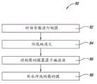
图7是例示一实施方案方法的流程图。Figure 7 is a flow diagram illustrating a method of an embodiment.
图8示出使用一实施方案的光刻胶构图方法的构图的膜的薄层电阻变化。Figure 8 shows the sheet resistance variation of a patterned film using the photoresist patterning method of an embodiment.
图9示出使用一实施方案的光刻胶构图方法的构图的膜的薄层电阻变化。Figure 9 shows the sheet resistance variation of a patterned film using the photoresist patterning method of an embodiment.
发明详述Detailed description of the invention
某些实施方案描述了对可包含金属纳米线的稀疏网络的纳米结构透明导体进行构图的方法。Certain embodiments describe methods of patterning nanostructured transparent conductors that may comprise sparse networks of metallic nanowires.
传导纳米结构conductive nanostructure
如本文所使用的,“传导纳米结构”或“纳米结构”通常是指导电的纳米尺寸的结构,该结构的至少一个维度(即,宽度或直径)小于500nm,并且更典型地,小于100nm或50nm。在多个实施方案中,纳米结构的宽度或直径在10至40nm、20至40nm、5至20nm、10至30nm、40至60nm、50至70nm的范围内。As used herein, "conducting nanostructure" or "nanostructure" generally refers to an electrically conductive nanoscale structure having at least one dimension (i.e., width or diameter) of less than 500 nm, and more typically, less than 100 nm or 50nm. In various embodiments, the width or diameter of the nanostructures is in the range of 10 to 40 nm, 20 to 40 nm, 5 to 20 nm, 10 to 30 nm, 40 to 60 nm, 50 to 70 nm.
纳米结构可以为任何形状或几何结构。一种定义给定纳米结构的几何结构的方法是通过其“长宽比”,“长宽比”是指纳米结构的长度与宽度(或直径)的比率。在某些实施方案中,纳米结构为各向同性形状(即,长宽比=1)。典型的各向同性或基本各向同性的纳米结构包括纳米颗粒。在优选的实施方案中,纳米结构为各向异性形状(即,长宽比≠1)。各向异性的纳米结构通常具有沿其长度的纵轴。示例性各向异性的纳米结构包括纳米线(具有至少10的长宽比,更典型地至少50的长宽比的实心纳米结构)、纳米棒(具有小于10的长宽比的实心纳米结构)以及纳米管(中空纳米结构)。Nanostructures can be of any shape or geometry. One way to define the geometry of a given nanostructure is by its "aspect ratio," which refers to the ratio of the nanostructure's length to width (or diameter). In certain embodiments, the nanostructures are isotropic in shape (ie, aspect ratio = 1). Typical isotropic or substantially isotropic nanostructures include nanoparticles. In preferred embodiments, the nanostructures are anisotropic in shape (ie, aspect ratio≠1). Anisotropic nanostructures typically have a longitudinal axis along their length. Exemplary anisotropic nanostructures include nanowires (solid nanostructures having an aspect ratio of at least 10, more typically at least 50), nanorods (solid nanostructures having an aspect ratio of less than 10) and nanotubes (hollow nanostructures).
在长度方向上,各向异性的纳米结构(例如,纳米线)的长度超过500nm,或超过1μm或者超过10μm。在多个实施方案中,纳米结构的长度在5至30μm的范围内、或在15至50μm的范围内、在25至75μm、30至60μm、40至80μm或50至100μm的范围内。In the length direction, the length of the anisotropic nanostructure (eg, nanowire) exceeds 500 nm, or exceeds 1 μm, or exceeds 10 μm. In various embodiments, the nanostructures have a length in the range of 5 to 30 μm, or in the range of 15 to 50 μm, in the range of 25 to 75 μm, 30 to 60 μm, 40 to 80 μm, or 50 to 100 μm.
纳米结构可以为任何传导材料。更典型地,纳米结构可由金属材料形成,金属材料包括单质金属(例如,过渡金属)或金属化合物(例如,金属氧化物)。金属材料也可以为双金属材料或金属合金,其包括两种或多种金属。适当的金属包括但不限于银、金、铜、镍、镀金的银、铂以及钯。应该注意,虽然本公开主要描述了纳米线(例如,银纳米线),但是同样也可采用以上定义的任何纳米结构。The nanostructures can be any conductive material. More typically, nanostructures may be formed from metallic materials, including elemental metals (eg, transition metals) or metal compounds (eg, metal oxides). Metallic materials may also be bimetallic materials or metal alloys, which include two or more metals. Suitable metals include, but are not limited to, silver, gold, copper, nickel, gold-plated silver, platinum, and palladium. It should be noted that while this disclosure primarily describes nanowires (eg, silver nanowires), any nanostructure defined above may equally be employed.
适当的纳米线的长宽比范围通常为10至100,000。更大的长宽比可利于得到透明导体层,这是因为更大的长宽比能够使更有效的传导网络形成,同时对于高透明度允许线的总密度更低。也就是说,当使用长宽比高的传导纳米线时,实现传导网络的纳米线的密度可足够低,以使得传导网络基本透明。Suitable nanowires typically have aspect ratios in the range of 10 to 100,000. A larger aspect ratio can be beneficial to obtain a transparent conductor layer because a larger aspect ratio enables a more efficient conductive network to form while allowing a lower overall density of lines for high transparency. That is, when high aspect ratio conductive nanowires are used, the density of nanowires implementing the conductive network may be low enough that the conductive network is substantially transparent.
传导纳米线包括金属纳米线和其它具有高长宽比(例如高于10)的传导颗粒。非金属纳米线的实例包括但不限于碳纳米管(CNT)、金属氧化物纳米线、传导聚合物纤维等。Conductive nanowires include metal nanowires and other conductive particles with high aspect ratios (eg, higher than 10). Examples of non-metallic nanowires include, but are not limited to, carbon nanotubes (CNTs), metal oxide nanowires, conductive polymer fibers, and the like.
如本文所用,“金属纳米线”是指包括金属单质、金属合金或金属化合物(包括金属氧化物)的金属线。金属纳米线的至少一个剖面尺寸小于500nm、小于200nm、更优选地小于100nm。如上所述,金属纳米线的长宽比(长度:直径)大于10,优选大于50,更优选大于100。适合的金属纳米线可基于任何金属,包括但不限于:银、金、铜、镍以及镀金的银。As used herein, "metal nanowire" refers to a metal wire including a metal element, a metal alloy, or a metal compound (including metal oxide). At least one cross-sectional dimension of the metal nanowire is less than 500 nm, less than 200 nm, more preferably less than 100 nm. As mentioned above, the metal nanowires have an aspect ratio (length:diameter) greater than 10, preferably greater than 50, more preferably greater than 100. Suitable metal nanowires may be based on any metal including, but not limited to: silver, gold, copper, nickel, and gold-plated silver.
金属纳米线可通过本领域已知的方法制备。具体地,可在存在多元醇(例如乙二醇)和聚乙烯吡咯烷酮的情况下,通过银盐(例如硝酸银)的溶液相还原来合成银纳米线。可根据例如Xia,Y.et al.,Chem.Mater.(2002),14,4736-4745以及Xia,Y.et al.,Nanoletters(2003)3(7),955-960中所描述的方法来准备相同尺寸的银纳米线的大规模生产。Metal nanowires can be prepared by methods known in the art. Specifically, silver nanowires can be synthesized by solution-phase reduction of silver salts such as silver nitrate in the presence of polyalcohols such as ethylene glycol and polyvinylpyrrolidone. According to the methods described in Xia, Y. et al., Chem. Mater. (2002), 14, 4736-4745 and Xia, Y. et al., Nanoletters (2003) 3 (7), 955-960, for example to prepare for mass production of silver nanowires of the same size.
传导层和衬底Conductive Layers and Substrates
作为说明性的实例,图1示出透明导体10,其包括涂布在衬底14上的传导层12。传导层12包括多个金属纳米线16。该金属纳米线16形成传导网络。As an illustrative example, FIG. 1 shows a
图2示出透明导体10’的另一个实例,其中在衬底14上形成传导层12’。传导层12’包括嵌在基质18中的多根金属纳米线16。Figure 2 shows another example of a transparent conductor 10' in which a conductive layer 12' is formed on a
“基质”,在某些语境中又被称为“粘合剂”,是指金属纳米线散布或嵌入其中的固态材料。部分纳米线可从基质材料中突出,从而能够通向(access to)传导网络。基质是金属纳米线的主体并且提供传导层的物理形式。基质保护金属纳米线免受不利的环境因素的影响,如腐蚀和磨损。具体地,基质显著地降低了环境中腐蚀性成分的渗透,如水分、痕量的酸、氧、硫等。A "matrix," also called a "binder" in some contexts, refers to a solid material in which metal nanowires are dispersed or embedded. Portions of the nanowires can protrude from the matrix material, enabling access to the conductive network. The matrix is the body of the metal nanowires and provides the physical form of the conductive layer. The matrix protects the metal nanowires from adverse environmental factors such as corrosion and abrasion. Specifically, the matrix significantly reduces the penetration of corrosive components in the environment, such as moisture, traces of acids, oxygen, sulfur, etc.
此外,基质使传导层具有良好的物理和力学性质。例如,其可附着于衬底。此外,与金属氧化物膜不同,嵌有金属纳米线的聚合物基质或有机基质坚固且柔韧。如本文将更详细讨论的,柔性基质能够以低成本和高产量的工艺制备透明导体。Furthermore, the matrix imparts good physical and mechanical properties to the conductive layer. For example, it can be attached to a substrate. Furthermore, unlike metal oxide films, polymer or organic matrices embedded with metal nanowires are strong and flexible. As will be discussed in more detail herein, flexible substrates enable the fabrication of transparent conductors in a low-cost and high-throughput process.
此外,可通过选择适当的基质材料来调整传导层的光学性质。例如,通过利用具有期望的折射率、组分和厚度的基质,可有效地减少反射损耗和不期望的眩光。Furthermore, the optical properties of the conducting layer can be tuned by choosing an appropriate matrix material. For example, reflection losses and undesired glare can be effectively reduced by utilizing a matrix with a desired refractive index, composition, and thickness.
典型地,基质是光学透明(optically clear)材料。如果在可见光区(400nm-700nm)材料的光透射率至少为80%,则可认为该材料是“光学清晰的”或者“光学透明的”。除另有说明外,本文中描述的透明导体中的所有层(包括衬底和纳米线网络层)都优选为光学透明的。典型地,基质的光学透明度由多种因素确定,包括但不限于:折射率(RI)、厚度、整个厚度的RI连续性、表面(包括界面)反射以及雾度(haze)(由表面粗糙度和/或嵌入的颗粒导致的散射损耗)。Typically, the matrix is an optically clear material. A material is considered "optically clear" or "optically transparent" if it transmits at least 80% of light in the visible region (400nm-700nm). Unless otherwise stated, all layers in the transparent conductors described herein, including the substrate and nanowire network layers, are preferably optically transparent. Typically, the optical clarity of a substrate is determined by a variety of factors, including but not limited to: Refractive Index (RI), thickness, RI continuity through thickness, surface (including interface) reflection, and haze (defined by surface roughness and/or scattering losses due to embedded particles).
在某些实施方案中,基质的厚度为约10nm至5μm、约20nm至1μm或约50nm至200nm。在其它实施方案中,基质的折射率约为1.3至2.5或约为1.35至1.8。In certain embodiments, the matrix has a thickness of about 10 nm to 5 μm, about 20 nm to 1 μm, or about 50 nm to 200 nm. In other embodiments, the matrix has a refractive index of about 1.3 to 2.5 or about 1.35 to 1.8.
在某些实施方案中,基质是聚合物,也称为聚合物基质。光学透明聚合物是本领域公知的。适当的聚合物基质的实例包括但不限于:诸如聚甲基丙烯酸酯(例如聚(甲基丙烯酸甲酯))、聚丙烯酸酯和聚丙烯腈的聚丙烯酸化物;聚乙烯醇;聚酯(例如,聚对苯二甲酸乙二醇酯(PET)、聚萘二甲酸酯和聚碳酸酯);具有高芳香度的聚合物,例如酚醛树脂或甲酚-甲醛


在其他实施方案中,本文描述的聚合物基质包括部分聚合的或部分固化的聚合物。与完全聚合的或完全固化的基质相比,部分固化的基质的交联程度和/或聚合度更低且分子量更小。因此,部分聚合的基质可以在某些条件下蚀刻,并且可能应用传统的光刻法进行构图。在适当的聚合条件下,可以对部分固化的基质进一步固化,从而进行进一步的交联和聚合,以提供比部分固化的基质更高分子量的基质。可以对部分固化的基质进行蚀刻,之后进行进一步固化的步骤,从而提供已构图且完全固化的透明导体膜。适当地部分固化的聚合物的实例包括但不限于:部分固化的丙烯酸酯、硅酮-环氧树脂、硅氧烷、酚醛清漆、环氧树脂、聚氨酯、硅倍半氧烷和聚酰亚胺。In other embodiments, the polymer matrices described herein include partially polymerized or partially cured polymers. A partially cured matrix is less crosslinked and/or polymerized and has a lower molecular weight than a fully polymerized or fully cured matrix. Thus, partially polymerized substrates can be etched under certain conditions and patterned using conventional photolithography. Under appropriate polymerization conditions, the partially cured matrix can be further cured to undergo further crosslinking and polymerization to provide a higher molecular weight matrix than the partially cured matrix. The partially cured matrix can be etched followed by a further curing step to provide a patterned and fully cured transparent conductor film. Examples of suitably partially cured polymers include, but are not limited to: partially cured acrylates, silicone-epoxys, silicones, novolacs, epoxies, polyurethanes, silsesquioxanes and polyimides .
本领域技术人员可以理解,聚合度会影响蚀刻条件(溶液),在该蚀刻条件下部分聚合的基质和/或纳米线可溶解。典型地,聚合度越高,就越难对基质进行蚀刻。Those skilled in the art will understand that the degree of polymerization will affect the etching conditions (solution) under which the partially polymerized matrix and/or nanowires can dissolve. Typically, the higher the degree of polymerization, the more difficult it is to etch the substrate.
优选地,部分固化的基质具有可接受的物理完整度,以保护其中的纳米线。这是所期望的,因为终端用户会进行其自身的构图以及之后的固化,从而获得最终的透明导体膜。Preferably, the partially cured matrix has acceptable physical integrity to protect the nanowires therein. This is expected since the end user will do its own patterning and subsequent curing to obtain the final transparent conductor film.
在其它的实施方案中,基质是无机材料。例如,可以使用基于硅石、莫来石、氧化铝、SiC、MgO-Al2O3-SiO2、Al2O3-SiO2、MgO-Al2O3-SiO2-Li2O或它们的混合物的溶胶-凝胶基质。In other embodiments, the matrix is an inorganic material. For example, silica, mullite, alumina, SiC, MgO-Al2 O3 -SiO2 , Al2 O3 -SiO2 , MgO-Al2 O3 -SiO2 -Li2 O or their The sol-gel matrix of the mixture.
在某些实施方案中,基质自身是传导性的。例如,基质可以是传导聚合物。传导聚合物是本领域公知的,包括但不限于:聚(3,4-乙烯基二氧噻吩)(PEDOT)、聚苯胺、聚噻吩和聚丁二炔。In certain embodiments, the matrix itself is conductive. For example, the matrix can be a conductive polymer. Conductive polymers are well known in the art and include, but are not limited to: poly(3,4-ethylenedioxythiophene) (PEDOT), polyaniline, polythiophene, and polydiacetylene.
“传导层”或“传导膜”是指提供透明导体的传导介质的金属纳米线的网络层。当存在基质时,金属纳米线的网络层与基质的组合也称为“传导层”。因为传导性是通过电荷从一根金属纳米线渗透到另一根金属纳米线而实现的,所以在传导层中必须存在足够的金属纳米线,从而达到电渗透阈值并变为传导性的。传导层的传导率与传导层的电阻率成反比,传导率有时称为薄层电阻,可用本领域公知的方法对表面传导率进行测量。"Conductive layer" or "conductive film" refers to a network layer of metallic nanowires that provides a conductive medium for transparent conductors. When a matrix is present, the combination of the network layer of metal nanowires and the matrix is also referred to as a "conducting layer". Because conductivity is achieved by charge percolation from one metal nanowire to another, enough metal nanowires must be present in the conducting layer to reach the electro-percolation threshold and become conductive. The conductivity of the conductive layer is inversely proportional to the resistivity of the conductive layer, sometimes referred to as sheet resistance, and surface conductivity can be measured by methods known in the art.
同样,当基质存在时,基质必须填充有足够的金属纳米线以变为传导性。如本文中所使用的,“阈值装填量”是指在装填传导层之后金属纳米线按重量的百分比,其中传导层的表面电阻率或面内电阻率不大于约106欧姆/平方(或Ω/□)。更为典型的是,表面电阻率不大于105Ω/□、不大于104Ω/□、不大于1000Ω/□、不大于500Ω/□或者不大于100Ω/□。阈值装填量取决于以下因素,如长宽比、定向度、团聚度以及金属纳米线的电阻率。Also, when a matrix is present, the matrix must be filled with enough metal nanowires to become conductive. As used herein, "threshold loading" refers to the percentage by weight of metal nanowires after loading a conductive layer having a surface or in-plane resistivity of not greater than about 106 ohms/square (or Ω /□). More typically, the surface resistivity is not greater than 105 Ω/□, not greater than 104 Ω/□, not greater than 1000 Ω/□, not greater than 500 Ω/□ or not greater than 100 Ω/□. The threshold loading depends on factors such as aspect ratio, degree of orientation, degree of agglomeration, and resistivity of the metal nanowires.
正如本领域技术人员所理解的那样,通过在其中高度装填任意颗粒,可能使基质的力学和光学性质发生改变或受到损害。有利地,金属纳米线的高长宽比使得对于银纳米线而言,在阈值表面装填量优选为约0.05μg/cm2至约10μg/cm2、更优选为约0.1μg/cm2至约5μg/cm2,更优选为约0.8μg/cm2至约3μg/cm2时形成穿过基质的传导网络。该装填量不影响基质的力学或光学性质。这些数值高度依赖于纳米线的尺寸和空间分散度。有利地,可通过调整金属纳米线的装填量来提供具有可调谐电导率(或表面电阻率)和光学透明度的透明导体。As will be appreciated by those skilled in the art, by highly packing it with arbitrary particles, the mechanical and optical properties of the matrix may be altered or compromised. Advantageously, the high aspect ratio of the metal nanowires is such that for silver nanowires, the threshold surface loading is preferably from about 0.05 μg/cm2 to about 10 μg/cm2 , more preferably from about 0.1 μg/cm2 to about 5 μg/
在某些实施方案中,保护层中的表面传导性可以通过在保护层中加入多个纳米尺寸的传导粒子来建立。如图3所示,在衬底14上沉积基于纳米线的传导层10。传导层10包括纳米线16,纳米线16达到渗透阈值并建立了面内传导性。在传导层10上形成保护层17。在保护层17中嵌入多个传导颗粒17a。有利地,纳米尺寸的传导颗粒在保护层中的装填水平无需达到渗透阈值而呈现表面传导性。传导层保持为当前承载的介质,该介质中的纳米线已经达到电渗透水平。保护层中的传导颗粒由于其与穿过保护层厚度的底部纳米线接触,因而提供表面传导性。In certain embodiments, surface conductivity in the protective layer can be established by incorporating a plurality of nano-sized conductive particles in the protective layer. As shown in FIG. 3 , a nanowire-based
因此,一个实施方案提供了多层结构,包括:衬底;形成在衬底上的传导层,其中传导层包括多根第一金属纳米线,所述多根第一金属线达到电渗透水平;以及形成在传导层上的保护层,保护层含有多个第二传导颗粒,所述多个第二传导颗粒低于电渗透水平。Accordingly, one embodiment provides a multilayer structure comprising: a substrate; a conductive layer formed on the substrate, wherein the conductive layer includes a plurality of first metal nanowires, the plurality of first metal wires achieving an electropermeable level; And a protective layer formed on the conductive layer, the protective layer contains a plurality of second conductive particles, the plurality of second conductive particles is below the electro-osmotic level.
如本文所用,纳米尺寸的传导颗粒是指至少一个维度不大于500nm、且更典型地不大于200nm的传导颗粒。适当的传导粒子的实例包括但不限于:ITO、ZnO、掺杂的ZnO、金属纳米线(包括本文所描述的那些)、金属纳米管、碳纳米管(CNT)等。As used herein, nano-sized conductive particles refer to conductive particles having at least one dimension no greater than 500 nm, and more typically no greater than 200 nm. Examples of suitable conductive particles include, but are not limited to: ITO, ZnO, doped ZnO, metal nanowires (including those described herein), metal nanotubes, carbon nanotubes (CNTs), and the like.
“衬底”或“选择的衬底”是指在其上涂布或层压透明导体的材料。衬底可以是刚性或柔性的。衬底可以是透明的或不透明的。如下文所讨论的,典型地,术语“选择的衬底”连同层压工艺一起使用。适当的刚性衬底包括:例如,玻璃、聚碳酸酯、丙烯酸树脂等。适当的柔性衬底包括但不限于:聚酯(例如聚对苯二甲酸乙二醇酯(PET)、聚萘二甲酸酯和聚碳酸酯)、聚烯烃(例如直链、支链和环状聚烯烃)、聚乙烯化合物(例如聚氯乙烯、聚偏二氯乙烯、聚乙烯醇缩乙醛、聚苯乙烯、聚丙烯酸酯等)、纤维素酯碱(例如三醋酸纤维素、醋酸纤维素)、诸如聚醚砜的聚砜、聚酰亚胺、硅酮以及其它常规聚合物膜。适当衬底的其它实例可以在例如第6,975,067号美国专利中找到。"Substrate" or "selected substrate" means the material on which the transparent conductor is coated or laminated. The substrate can be rigid or flexible. The substrate can be transparent or opaque. As discussed below, typically the term "selected substrate" is used in connection with the lamination process. Suitable rigid substrates include, for example, glass, polycarbonate, acrylic, and the like. Suitable flexible substrates include, but are not limited to: polyesters (such as polyethylene terephthalate (PET), polyethylene naphthalate, and polycarbonate), polyolefins (such as linear, branched, and cyclic polyolefins), polyvinyl compounds (e.g. polyvinyl chloride, polyvinylidene chloride, polyvinyl acetal, polystyrene, polyacrylate, etc.), cellulose ester bases (e.g. cellulose triacetate, cellulose acetate element), polysulfone such as polyethersulfone, polyimide, silicone, and other conventional polymer membranes. Other examples of suitable substrates can be found, for example, in US Patent No. 6,975,067.
典型地,传导层的光学透明度或清晰度可由以下参数定量地限定,包括光透射率和雾度。“光透射率”(或者“透光率”)是指通过介质传输的入射光的百分比。在多个实施方案中,传导层的光透射率至少为80%,并且可高达98%。对于其中的传导层沉积或层压在衬底上的透明导体,整个结构的光透射率可能略有减小。诸如粘合层、防反射层、防眩光层的性能增强层可进一步有助于减小透明导体的总的光透射率。在多个实施方案中,透明导体的光透射率(“T%”)可以是至少50%、至少60%、至少70%或至少80%,并且可以高达至少91%至92%,或至少95%。。Typically, the optical clarity or clarity of the conductive layer can be quantitatively defined by parameters including light transmission and haze. "Light transmission" (or "light transmission") refers to the percentage of incident light that is transmitted through a medium. In various embodiments, the light transmission of the conductive layer is at least 80%, and can be as high as 98%. For transparent conductors in which the conductive layer is deposited or laminated on the substrate, the light transmission of the entire structure may be slightly reduced. Performance enhancing layers such as adhesive layers, anti-reflection layers, anti-glare layers can further contribute to reducing the overall light transmission of the transparent conductor. In various embodiments, the light transmission ("T%") of the transparent conductor can be at least 50%, at least 60%, at least 70%, or at least 80%, and can be as high as at least 91% to 92%, or at least 95%. %. .
雾度(“H%”)是光漫射的指数。雾度是指从入射光中分离出来并在传输的过程中散射的光的数量百分比。光透射在很大程度上是介质的性质,与之不同的是,雾度经常和产品有关,且典型地是由表面粗糙度和介质中的嵌入颗粒或组分不均匀性所导致的。典型地,传导膜的雾度可能明显地受到纳米结构的直径的影响。更大直径的纳米结构(例如,更粗的纳米线)通常与更高的雾度关联。在多个实施方案中,透明导体的雾度不超过10%、不超过8%或不超过5%,并可低至不超过2%、不超过1%,不超过0.5%,或不超过0.25%。Haze ("H%") is an index of light diffusion. Haze is the percentage of light that is separated from incident light and scattered during transmission. Unlike light transmission, which is largely a property of the media, haze is often product-dependent and is typically caused by surface roughness and embedded particles or component inhomogeneities in the media. Typically, the haze of a conductive film can be significantly affected by the diameter of the nanostructures. Larger diameter nanostructures (eg, thicker nanowires) are generally associated with higher haze. In various embodiments, the haze of the transparent conductor is no more than 10%, no more than 8%, or no more than 5%, and can be as low as no more than 2%, no more than 1%, no more than 0.5%, or no more than 0.25 %.
纳米线的沉积和透明导体的制备Deposition of nanowires and preparation of transparent conductors
因此,在某些实施方案中,本文描述了制备透明导体的方法,包括:在衬底上沉积多根金属纳米线,所述金属纳米线分散在流体中;以及通过使该流体干燥而在衬底上形成金属纳米线网络层。Accordingly, in certain embodiments, described herein are methods of making a transparent conductor comprising: depositing a plurality of metal nanowires on a substrate, the metal nanowires being dispersed in a fluid; A metal nanowire network layer is formed on the bottom.
金属纳米线可以如上文所述的那样制备。金属纳米线典型地分散在液体中以便于沉积。应当理解,如本文所用,“沉积”和“涂布”可以互换使用。金属纳米线在其中可形成稳定分散体(也称为“金属纳米线分散体”)的任何非腐蚀性液体都可以使用。优选地,金属纳米线分散在水、酒精、酮、醚、碳氢化合物或芳香族溶剂(苯、甲苯、二甲苯等)中。更优选地,该液体是挥发性的,沸点不超过200°C,不超过150°C或不超过100°C。Metal nanowires can be prepared as described above. Metal nanowires are typically dispersed in a liquid to facilitate deposition. It should be understood that, as used herein, "deposition" and "coating" are used interchangeably. Any non-corrosive liquid in which the metal nanowires can form a stable dispersion (also referred to as a "metal nanowire dispersion") can be used. Preferably, the metal nanowires are dispersed in water, alcohols, ketones, ethers, hydrocarbons or aromatic solvents (benzene, toluene, xylene, etc.). More preferably, the liquid is volatile and has a boiling point of no more than 200°C, no more than 150°C or no more than 100°C.
此外,金属纳米线分散体可含有添加剂和粘合剂以控制粘度、腐蚀性、附着力以及纳米线分散体。适当的添加剂和粘合剂的实例包括但不仅限于,羧甲基纤维素(CMC),2-羟乙基纤维素(HEC),羟丙基甲基纤维素(HPMC),甲基纤维素(MC),聚乙烯醇(PVA),三丙二醇(TPG)和黄原胶(XG),以及诸如乙氧基化物、烷氧基化物、环氧乙烷和环氧丙烷及它们的共聚物、磺酸盐、硫酸盐、二磺酸盐、磺基琥珀酸盐、磷酯以及氟表面活性剂(例如,DuPont的
在一个实例中,按重量计算,纳米线分散体或“油墨”包含0.0025%至0.1%的表面活性剂(例如,对于


分散体中的纳米线浓度可以影响或决定纳米线网络层的参数,诸如厚度、传导率(包括表面传导率)、光透射率以及机械性能。可以调整溶剂的百分比,从而在分散体中提供所需的纳米线浓度。然而,在更优选的实施方案中,其它成分的相对比率可保持不变。具体地,表面活性剂相对于粘度调节剂的比率优选为约80比约0.01;粘度调节剂相对于金属纳米线的比率优选为约5比约0.000625;以及金属纳米线相对于表面活性剂的比率优选为约560比约5。分散体成分的比率可根据使用的衬底及应用方法而修改。对于用于沉积的纳米线分散体,优选的粘度范围为约1至100cP。The nanowire concentration in the dispersion can affect or determine parameters of the nanowire network layer, such as thickness, conductivity (including surface conductivity), light transmission, and mechanical properties. The percentage of solvent can be adjusted to provide the desired concentration of nanowires in the dispersion. However, in more preferred embodiments, the relative ratios of the other ingredients may remain unchanged. Specifically, the ratio of surfactant to viscosity modifier is preferably about 80 to about 0.01; the ratio of viscosity modifier to metal nanowires is preferably about 5 to about 0.000625; and the ratio of metal nanowires to surfactant About 560 to about 5 is preferred. The ratios of the dispersion components can be modified according to the substrate used and the method of application. For nanowire dispersions for deposition, the preferred viscosity range is about 1 to 100 cP.
在沉积之后,液体通过蒸发而除去。蒸发可通过加热(例如烘烤)而加快。产生的纳米线网络层可能需要后处理以使其能够导电。该后处理可以是下述工序,其涉及暴露于热、等离子体、电晕放电、UV臭氧或如下文所述的压力。After deposition, the liquid is removed by evaporation. Evaporation can be accelerated by heating, such as baking. The resulting nanowire network layer may require post-processing to render it conductive. This post-treatment may be a procedure involving exposure to heat, plasma, corona discharge, UV ozone or pressure as described below.
因此,在某些实施方案中,本文描述了制备透明导体的方法,包括:在衬底上沉积多个金属纳米线,所述金属纳米线分散在流体中;通过使流体干燥而在衬底上形成金属纳米线网络层,在该金属纳米线网络层上涂布基质材料,以及使该基质材料固化以形成基质。Accordingly, in certain embodiments, described herein are methods of making a transparent conductor comprising: depositing a plurality of metal nanowires on a substrate, the metal nanowires being dispersed in a fluid; A metal nanowire network layer is formed, a matrix material is coated on the metal nanowire network layer, and the matrix material is cured to form a matrix.
如本文所定义的,“基质材料”是指能够固化为基质的材料或材料的混合物。“使固化”或“固化”是指这样的工艺,其中单体或部分聚合物(少于150个单体)聚合和/或交联以形成固态聚合物基质。适当的聚合条件是本领域公知的,作为实例其包括,对单体进行加热,用可见光或紫外(UV)光、电子束辐射单体,等。此外,同时由去除溶剂造成的聚合物/溶剂体系的“凝固”也在“固化”的意义范围内。As defined herein, "matrix material" means a material or mixture of materials capable of curing into a matrix. "Curing" or "curing" refers to a process in which monomers or portions of polymers (less than 150 monomers) are polymerized and/or crosslinked to form a solid polymer matrix. Suitable polymerization conditions are well known in the art and include, by way of example, heating the monomer, irradiating the monomer with visible or ultraviolet (UV) light, electron beams, and the like. Furthermore, the concomitant "solidification" of the polymer/solvent system resulting from the removal of the solvent is also within the meaning of "curing".
固化程度可以通过选择单体的初始浓度以及交联剂的量来控制。固化程度还可以通过调节固化参数(诸如用于聚合的时间以及发生聚合的温度等等)来操纵。在某些实施方案中,可以对部分固化的基质进行淬火,以停止固化过程。固化程度或聚合度可以通过例如固化聚合物的分子量或者通过位于表示活性化学物的波长处的光学吸收来监控。The degree of cure can be controlled by selecting the initial concentration of monomers and the amount of crosslinker. The degree of cure can also be manipulated by adjusting cure parameters such as the time for polymerization and the temperature at which polymerization occurs, among others. In some embodiments, the partially cured matrix can be quenched to stop the curing process. The degree of cure or polymerization can be monitored by, for example, the molecular weight of the cured polymer or by optical absorption at wavelengths indicative of active chemicals.
因此,在某些实施方案中,基质材料包括可以完全或部分固化的聚合物。光学透明聚合物是本领域公知的。适当的聚合物基质的实例包括但不限于:诸如聚甲基丙烯酸酯、聚丙烯酸酯和聚丙烯腈的聚丙烯酸酯(或“丙烯酸酯”);聚乙烯醇;聚酯(例如,聚对苯二甲酸乙二醇酯(PET)、聚萘二甲酸酯和聚碳酸酯);具有高度芳香性的聚合物,例如酚醛树脂或甲酚-甲醛


在优选的实施方案中,预聚物是可光固化的,即该预聚物通过暴露于辐射而聚合和/或交联。如将会更详细描述的那样,基于可光固化预聚物的基质可通过在选择性区域中暴露于辐射而被构图。在其它的实施方案中,预聚物是可热固化的,其可以通过选择性暴露于热源而被构图。In a preferred embodiment, the prepolymer is photocurable, ie the prepolymer polymerizes and/or crosslinks by exposure to radiation. As will be described in more detail, photocurable prepolymer based substrates can be patterned by exposure to radiation in selected areas. In other embodiments, the prepolymer is thermally curable, which can be patterned by selective exposure to a heat source.
通常,基质材料是液体。基质材料任选包含溶剂。任何能有效地使基质材料溶剂化或分散的非腐蚀性溶剂都可以使用。适当的溶剂的实例包括水、酒精、酮、四氢呋喃、碳氢化合物(例如环己烷)或芳烃溶剂(苯、甲苯、二甲苯等)。更优选地,该溶剂是挥发性的,其沸点不超过200°C、不超过150°C或者不超过100°C。Typically, the matrix material is a liquid. The matrix material optionally contains a solvent. Any non-corrosive solvent effective to solvate or disperse the matrix material can be used. Examples of suitable solvents include water, alcohols, ketones, tetrahydrofuran, hydrocarbons (such as cyclohexane) or aromatic solvents (benzene, toluene, xylene, etc.). More preferably, the solvent is volatile with a boiling point of no more than 200°C, no more than 150°C, or no more than 100°C.
在某些实施方案中,基质材料可包括交联剂、聚合引发剂、稳定剂(例如,包括抗氧化剂、用于更长的产品寿命的UV稳定剂,以及用于更大的搁置寿命的聚合抑制剂)、表面活性剂等。在其它的实施方案中,基质材料可进一步包括防腐剂。In certain embodiments, the matrix material may include crosslinkers, polymerization initiators, stabilizers (e.g., including antioxidants, UV stabilizers for longer product life, and polymerization for greater shelf life). Inhibitors), surfactants, etc. In other embodiments, the matrix material may further include a preservative.
如本文所述,可通过例如板带涂布、湿涂、印刷和层压制备透明导体。As described herein, transparent conductors can be prepared by, for example, tape coating, wet coating, printing, and lamination.
从传导纳米结构制造透明导体公开于,例如,美国专利申请第11/871,767号,通过引用将其整体并入本文。Fabrication of transparent conductors from conductive nanostructures is disclosed, for example, in US Patent Application Serial No. 11/871,767, which is incorporated herein by reference in its entirety.
构图composition
可以通过蚀刻对传导层进行构图。根据传导层的成分,多种蚀刻溶液或“蚀刻剂”可用于溶解并除去传导层在暴露区域中的部分。蚀刻剂可以以任何已知方法应用到待构图的透明导体上,包括使用预定构图的掩模或以预定图案丝网印刷蚀刻剂。The conductive layer can be patterned by etching. Depending on the composition of the conductive layer, a variety of etching solutions or "etches" can be used to dissolve and remove portions of the conductive layer in exposed areas. The etchant may be applied to the transparent conductor to be patterned by any known method, including using a predetermined patterned mask or screen printing the etchant in a predetermined pattern.
在一个实施方案中,可以应用包括硝酸(HNO3)的酸蚀刻溶液。典型地,硝酸为0.01%-40%,更典型地,硝酸为0.01%-10%。酸蚀刻溶液可以进一步包括痕量(例如,约1-100ppm)的高锰酸钾(KMnO4)。在一个实施方案中,酸蚀刻溶液包括约1%的HNO3、1%的NaNO3以及痕量(百万分之几)的高锰酸钾(KMnO4)。蚀刻溶液将金属纳米线转化为可溶的金属盐,该金属盐可以通过清洗而除去。例如,银纳米线可以转化为银盐(Ag+),银盐可以由例如水的溶剂冲洗掉。In one embodiment, an acid etch solution including nitric acid (HNO3 ) may be used. Typically, the nitric acid is 0.01%-40%, more typically, the nitric acid is 0.01%-10%. The acid etching solution may further include potassium permanganate (KMnO4 ) in trace amounts (eg, about 1-100 ppm). In one embodiment, the acid etch solution includes about 1% HNO3 , 1% NaNO3 , and traces (parts per million) of potassium permanganate (KMnO4 ). The etching solution converts the metal nanowires into soluble metal salts, which can be removed by washing. For example, silver nanowires can be converted to silver salts (Ag+ ), which can be washed away by a solvent such as water.
在某些实施方案中,蚀刻溶液不影响或溶解由完全或部分固化的聚合物所组成的基质。可以通过根据所需图案将聚合基质材料沉积并固化在纳米线层上来进行构图。一旦将基质固化(完全或者部分地)以达到可接受的硬度和物理形状,则基质保护嵌在其中的纳米线在随后的蚀刻步骤中不被蚀刻掉。未保护区域(其中,基质材料未聚合或者不存在基质)中的纳米线可以被蚀刻并除去。因此,一个实施方案描述了构图的方法,该方法包括:在衬底上形成传导层,该传导层包括多根纳米线;根据图案在传导层上形成基质,该图案包括由基质保护的纳米线以及未保护的纳米线;以及对传导层进行蚀刻以溶解未保护的纳米线。未保护的纳米线可以被除去或留在适当的位置。In certain embodiments, the etching solution does not affect or dissolve a matrix composed of a fully or partially cured polymer. Patterning can be performed by depositing and curing a polymeric matrix material on the nanowire layer according to the desired pattern. Once the matrix is cured (fully or partially) to an acceptable hardness and physical shape, the matrix protects the nanowires embedded therein from being etched away during subsequent etching steps. Nanowires in unprotected areas (where the matrix material is not polymerized or the matrix is absent) can be etched and removed. Accordingly, one embodiment describes a method of patterning comprising: forming a conductive layer on a substrate, the conductive layer including a plurality of nanowires; forming a matrix on the conductive layer according to a pattern, the pattern including nanowires protected by the matrix and the unprotected nanowires; and etching the conductive layer to dissolve the unprotected nanowires. Unprotected nanowires can be removed or left in place.
已经发现,本文描述的酸蚀刻溶液中的KMnO4的量可影响蚀刻能力。例如,酸蚀刻溶液中的KMnO4的量可影响蚀刻速率。典型地,KMnO4的浓度越高,蚀刻就越快。因此,对酸蚀刻溶液中的KMnO4的浓度的调节可调整蚀刻效率,而无需改变蚀刻溶液的酸度。It has been found that the amount ofKMnO4 in the acid etching solutions described herein can affect the etchability. For example, the amount ofKMnO4 in the acid etch solution can affect the etch rate. Typically, the higher the concentration ofKMnO4 , the faster the etch. Therefore, adjustments to the concentration ofKMnO4 in the acid etching solution can tune the etching efficiency without changing the acidity of the etching solution.
还已经观察到,酸蚀刻溶液中的KMnO4的浓度越高会使得蚀刻溶液越有效地扩散到基质中,这导致纳米线更快或更完全的原位溶解。例如,当蚀刻溶液中的KMnO4小于20ppm时,基质(标准厚度约为150nm)可保护嵌在其中的纳米线免受蚀刻。当KMnO4的量增加至约20ppm,而HNO3和NaNO3的浓度保持不变时,蚀刻溶液扩散到基质(厚度约为150nm)中并将嵌在其中的纳米线溶解。It has also been observed that higher concentrations ofKMnO4 in the acid etching solution lead to more efficient diffusion of the etching solution into the matrix, which leads to faster or more complete in situ dissolution of the nanowires. For example, when theKMnO4 in the etching solution is less than 20ppm, the matrix (standard thickness is about 150nm) can protect the nanowires embedded in it from etching. When the amount ofKMnO4 was increased to about 20 ppm while the concentrations ofHNO3 andNaNO3 were kept constant, the etching solution diffused into the matrix (about 150 nm in thickness) and dissolved the nanowires embedded therein.
较厚的保护层(约1μm)可有效地阻止酸蚀刻溶液的扩散并保护纳米线免受蚀刻,而未由该较厚的保护层保护的纳米线/基质则被酸蚀刻溶液(例如,20ppm的KMnO4、1%的HNO3以及1%的NaNO3)溶解。A thicker protective layer (approximately 1 μm) can effectively block the diffusion of acid etching solution and protect the nanowires from etching, while the nanowires/substrate not protected by this thicker protective layer are blocked by the acid etching solution (e.g., 20ppm KMnO4 , 1% HNO3 and 1% NaNO3 ) dissolved.
因此,在一个实施方案中,可选择能够扩散到基质中并将纳米线溶解的蚀刻溶液。在这些实施方案中,可以使用保护掩模(例如,光刻胶)对基质中包含纳米线的传导层进行蚀刻。因而,可以根据标准的光刻方法来进行构图,通过该光刻方法对暴露区域中的纳米线进行蚀刻。Therefore, in one embodiment, an etching solution can be chosen that is capable of diffusing into the matrix and dissolving the nanowires. In these embodiments, the conductive layer comprising the nanowires in the matrix can be etched using a protective mask (eg, photoresist). Thus, patterning can be performed according to standard photolithographic methods by which the nanowires in the exposed areas are etched.
在另一实施方案中,对暴露区域进行蚀刻包括:利用第一蚀刻剂对暴露区域中的基质进行蚀刻;以及利用第二蚀刻剂对暴露区域中的纳米线进行蚀刻。例如,第一蚀刻剂(例如,过氧化氢)可用于除去基质,从而在暴露区域中使纳米线暴露或脱保护。此后,第二蚀刻剂(诸如本文中所讨论的酸蚀刻溶液)可以用于溶解或除去不再由基质保护的纳米线。In another embodiment, etching the exposed area includes: etching the matrix in the exposed area with a first etchant; and etching the nanowires in the exposed area with a second etchant. For example, a first etchant (eg, hydrogen peroxide) can be used to remove the matrix, thereby exposing or deprotecting the nanowires in the exposed areas. Thereafter, a second etchant, such as the acid etching solution discussed herein, can be used to dissolve or remove the nanowires that are no longer protected by the matrix.
因此,其他实施方案描述了利用掩模对透明导体进行构图的方法。掩模作为较厚的保护层,保护下面的纳米线/基质层。该方法包括:在衬底上形成传导层,该传导层包括基质以及嵌在该基质中的多根导电纳米线;在传导层上放置掩模以限定掩模区域和暴露区域;以及利用酸蚀刻溶液对暴露区域进行蚀刻以形成构图的传导区域。该方法可进一步包括除去所蚀刻的区域以形成图案。Accordingly, other embodiments describe methods of patterning transparent conductors using masks. The mask acts as a thicker protective layer, protecting the underlying nanowire/substrate layer. The method includes: forming a conductive layer on a substrate, the conductive layer including a matrix and a plurality of conductive nanowires embedded in the matrix; placing a mask on the conductive layer to define masked areas and exposed areas; and etching with an acid The solution etches the exposed areas to form patterned conductive areas. The method may further include removing the etched regions to form a pattern.
能够对蚀刻效率产生贡献的其他因素包括但不限于基质的固化程度。例如,给定了相同的蚀刻溶液和相同的单体,由部分固化的聚合物所形成的基质趋于比由完全固化的聚合物所形成的基质更易于溶解。在构图之后,部分固化的基质可经历额外的固化步骤以将基质完全固化。Other factors that can contribute to etch efficiency include, but are not limited to, the degree of curing of the substrate. For example, given the same etching solution and the same monomers, matrices formed from partially cured polymers tend to dissolve more readily than matrices formed from fully cured polymers. After patterning, the partially cured matrix can undergo additional curing steps to fully cure the matrix.
还可以通过在蚀刻之前使透明导体的蚀刻表面活化而实现更有效的蚀刻。这种预处理尤其有益于湿法刻蚀工艺,在该工艺中,液体蚀刻剂与透明导体的蚀刻表面相接触。典型地,透明导体的蚀刻表面可以是纳米线/基质层的顶部表面,或者在某些情况下,可以是保护层的顶部表面。基质层和保护层保护下面的纳米线免受腐蚀成分以及磨损的影响。然而,基质层和保护层的存在会导致液体蚀刻剂较差的湿润。透明导体的蚀刻表面的预处理可以使表面活化并提高其湿润性。因此,液体蚀刻剂能够通向由基质和/或保护层保护的金属纳米线。More efficient etching can also be achieved by activating the etched surface of the transparent conductor prior to etching. This pretreatment is particularly beneficial for wet etch processes in which a liquid etchant is brought into contact with the etched surface of the transparent conductor. Typically, the etched surface of the transparent conductor may be the top surface of the nanowire/matrix layer, or in some cases, the top surface of the protective layer. The matrix layer and protective layer protect the underlying nanowires from corrosive components as well as abrasion. However, the presence of a matrix layer and a protective layer leads to poor wetting by liquid etchant. Pretreatment of etched surfaces of transparent conductors can activate the surface and improve its wettability. Thus, liquid etchant is able to access the metal nanowires protected by the matrix and/or protective layer.
因此,上述的构图方法可以进一步包括:对传导层的蚀刻表面进行预处理,以提高其湿润性。Therefore, the above patterning method may further include: pre-treating the etched surface of the conductive layer to improve its wettability.
湿润性的改变可以通过水接触角测量来评定。水接触角是指液体/蒸汽界面与固体表面(即,蚀刻表面)相交的角度。典型地,水接触角越大,固体表面的湿润越差。如表1所示,根据处理的类型,在表面处理后,水接触角基本上减少约50%至80%。Changes in wettability can be assessed by water contact angle measurements. The water contact angle is the angle at which a liquid/vapour interface intersects a solid surface (ie, an etched surface). Typically, the larger the water contact angle, the poorer the wetting of the solid surface. As shown in Table 1, the water contact angle is substantially reduced by about 50% to 80% after surface treatment, depending on the type of treatment.
表1Table 1

利用强度相同的蚀刻剂,与对未经处理的透明导体进行蚀刻速率相比,对经过表面处理的透明导体进行蚀刻的速率明显提高。因此,可以通过对待蚀刻区域进行预处理而有效地对透明导体膜进行构图。Using an etchant of the same strength, the etching rate of the surface-treated transparent conductor is significantly increased compared to the etching rate of the untreated transparent conductor. Therefore, the transparent conductor film can be effectively patterned by pre-treating the region to be etched.
此外,通过调节蚀刻剂的类型和/或强度,能够产生光学性质基本一致的或具有低可见度图案的经构图的透明导体膜。这些具有低可见度图案的透明导体作为诸如触摸屏的显示器的部件尤其有用。Furthermore, by adjusting the type and/or strength of the etchant, it is possible to produce patterned transparent conductor films with substantially uniform optical properties or low visibility patterns. These transparent conductors with low visibility patterns are especially useful as components of displays such as touch screens.
如本文所使用的,“基本光学一致”、“光学一致”或“光学一致性”是指具有至少两个不同传导性的区域的、经构图的透明导体膜的光学特性,被蚀刻区域的电阻率与未蚀刻区域的电阻率之比至少为103、或至少为104、或至少为105、或至少为106,其中两个区域的光透射率(T%)之差小于5%、或小于4%、或小于3%、或小于2%、或小于1%、或小于0.5%或为零;以及其中两个区域的雾度值(H%)之差小于0.5%、小于0.1%、小于0.07%、小于0.05%、小于0.03%、小于0.01%或为零。将经构图的传导膜的被蚀刻区域与未蚀刻区域之间的光学差异最小化或消除的过程也被称为“低可见度构图”。在这些情况下,可以相信,纳米线不会完全蚀刻掉或溶解,然而已经使蚀刻区域中的纳米线网络的传导性比未蚀刻区域中的纳米线网络的传导性更低。与本文所描述的“低可见度构图”相比,基本或完全溶解传导介质(例如,金属纳米线)的蚀刻工艺导致因光散射的减少而使被蚀刻区域的雾度大大下降,在这种情况下,被蚀刻区域与未蚀刻区域之间的光学差异可足以使被蚀刻图案更清楚地可见。As used herein, "substantially optically consistent", "optical uniform" or "optical uniformity" refers to the optical properties of a patterned transparent conductor film having at least two regions of different conductivity, the resistivity of the etched regions The ratio of the resistivity to the resistivity of the unetched area is at least 103 , or at least 104 , or at least 105 , or at least 106 , wherein the difference in light transmission (T%) of the two areas is less than 5% , or less than 4%, or less than 3%, or less than 2%, or less than 1%, or less than 0.5%, or zero; and the difference between the haze values (H%) of the two areas is less than 0.5%, less than 0.1 %, less than 0.07%, less than 0.05%, less than 0.03%, less than 0.01%, or zero. The process of minimizing or eliminating optical differences between etched and unetched regions of a patterned conductive film is also referred to as "low visibility patterning." In these cases, it is believed that the nanowires do not etch away or dissolve completely, but have made the nanowire network in the etched region less conductive than the nanowire network in the unetched region. Etching processes that substantially or completely dissolve the conductive medium (e.g., metal nanowires) result in a greatly reduced haze in the etched area due to reduced light scattering compared to the "low visibility patterning" described herein, in this case In this case, the optical difference between the etched and unetched areas may be sufficient to make the etched pattern more clearly visible.
因此,在另一实施方案中,可以通过产生非传导性区域或者具有改变的电阻率(不必是非传导性的)的区域而对传导层进行构图,而无需完全毁坏或除去纳米线。这样,被蚀刻区域的光学特性(即,透射率和雾度)的任何改变都可以相对最小,但在被蚀刻的区域中根据预定的图案改变传导介质(即,互连的纳米线网络)的电阻率。更具体地,该实施方案提供的方法包括:在衬底上形成传导层,该传导层包括基质和嵌在其中的导电纳米线的网络;以及处理该传导层的区域,以改变该区域内的导电纳米线网络的电阻率,从而形成经构图的传导层,该传导层包括具有第一电阻率的已处理区域和具有第二电阻率的未处理区域。已处理区域可以但不必是非传导性的。如本文中所用,“非传导性的”是指表面电阻率至少为106Ω/□。在某些实施方案中,第一电阻率与第二电阻率之比至少为1000(即,被蚀刻区域的传导性小于未蚀刻区域的传导性)。在其他一些实施方案中,第一电阻率与第二电阻率之比至少为104、或至少为105、或至少为106。Thus, in another embodiment, the conductive layer can be patterned without completely destroying or removing the nanowires by creating non-conductive regions or regions of altered resistivity (not necessarily non-conductive). In this way, any changes in the optical properties (i.e., transmittance and haze) of the etched area can be relatively minimal, but the conductivity of the conductive medium (i.e., the interconnected nanowire network) is changed according to a predetermined pattern in the etched area. resistivity. More specifically, this embodiment provides a method comprising: forming a conductive layer on a substrate, the conductive layer comprising a matrix and a network of conductive nanowires embedded therein; and treating a region of the conductive layer to alter the resistivity of the conductive nanowire network, thereby forming a patterned conductive layer comprising treated regions having a first resistivity and untreated regions having a second resistivity. The treated area can but need not be non-conductive. As used herein, "non-conductive" means having a surface resistivity of at least 106 Ω/□. In certain embodiments, the ratio of the first resistivity to the second resistivity is at least 1000 (ie, etched regions are less conductive than unetched regions). In other embodiments, the ratio of the first resistivity to the second resistivity is at least 104 , or at least 105 , or at least 106 .
此外,公开了包括衬底和经构图的传导层的透明导体,该传导层具有嵌在基质中的导电纳米线的网络。经构图的传导层限定出透明导体的第一区域以及透明导体的第二区域,在第一区域中,该网络具有第一电阻率,在第二区域中,该网络具有第二电阻率。两个区域之间的光学特性(即,透射率和雾度)的改变或差异相对较小。例如但不限于,第一区域和第二区域的透射率和雾度的差别分别小于0.7%和0.62%,而这两个区域之间的电阻的变化大于约1500Ω/□。Furthermore, a transparent conductor comprising a substrate and a patterned conductive layer having a network of conductive nanowires embedded in a matrix is disclosed. The patterned conductive layer defines a first region of transparent conductor in which the network has a first resistivity and a second region of transparent conductor in which the network has a second resistivity. The change or difference in optical properties (ie, transmittance and haze) between the two regions is relatively small. For example and without limitation, the difference in transmittance and haze of the first and second regions is less than 0.7% and 0.62%, respectively, while the change in resistance between the two regions is greater than about 1500 Ω/□.
如本文所述,可以根据本文描述的构图方法处理或蚀刻光学透明的传导层,而不会影响所处理或所蚀刻的区域的光学性质。如在实施例14中进一步示出的那样,光学性质的改变,包括透射率(T%)和雾度(H%),在构图步骤之前和之后都相对较小,从而所获得的被蚀刻图案具有低可见度。在这种“不可见构图”或“低可见度构图”方法中,传导层在外表上保持光学一致性;但根据预定的图案在未经处理(或未蚀刻)的区域中为传导的,已处理或已蚀刻的区域为非传导的或具有不同且较低的传导率。在本实施方案中,改变纳米线网络的电阻率可以通过以下方法来完成(但不限于):破坏或降低纳米线之间的连接的导电率,或者使纳米线本身成为非传导性的。在一个实施方案中,对导电纳米线网络的处理包括将导电纳米线在化学上转化为非传导性的纳米线或具有更高电阻率的线。这样的化学转化可包括例如氧化、硫化或者任何其他的将纳米线的下层传导材料转化为电绝缘材料的工艺。例如,由单质金属或金属合金(例如银)形成的传导性纳米线可以在该金属转化为电绝缘且不可溶的金属盐(例如,氯化银)时成为非传导性的。在该实施例中,单质银可以被初始地氧化并转化为银粒子(Ag+)。在存在阴离子(例如,Cl-)的情况下,可以为了完成而进一步驱动氧化,带正电的银离子可以与阴离子形成不可溶的盐(AgCl)。易于将金属离子沉淀为不可溶的金属盐的阴离子的其他实例包括,例如溴、碘和硫酸根。As described herein, optically transparent conductive layers may be treated or etched according to the patterning methods described herein without affecting the optical properties of the treated or etched regions. As further shown in Example 14, the changes in optical properties, including transmittance (T%) and haze (H%), are relatively small before and after the patterning step, so that the obtained etched patterns Has low visibility. In this "invisible patterning" or "low visibility patterning" approach, the conductive layer remains optically consistent in appearance; Or the etched area is non-conductive or has a different and lower conductivity. In this embodiment, altering the resistivity of the nanowire network can be accomplished by, but not limited to, disrupting or reducing the conductivity of the connections between the nanowires, or making the nanowires themselves non-conductive. In one embodiment, the treatment of the conductive nanowire network includes chemically converting the conductive nanowires to non-conductive nanowires or wires with higher resistivity. Such chemical conversion may include, for example, oxidation, sulfurization, or any other process that converts the underlying conductive material of the nanowires to an electrically insulating material. For example, conductive nanowires formed from an elemental metal or metal alloy (eg, silver) can become non-conductive when the metal is converted to an electrically insulating and insoluble metal salt (eg, silver chloride). In this embodiment, elemental silver may be initially oxidized and converted into silver particles (Ag+ ). Oxidation can be further driven to completion in the presence of anions (eg, Cl− ), with which positively charged silver ions can form insoluble salts (AgCl). Other examples of anions that readily precipitate metal ions as insoluble metal salts include, for example, bromine, iodine, and sulfate.
适当的氧化剂的实例包括但不限于:过氧化物(例如过氧化氢)、过硫酸盐(例如过硫酸铵)、过氧化合物(例如过氧二硫酸钠或过氧二硫酸钾)、卤素或基于卤素的氧化盐(例如氯盐或次氯酸盐)、氧化金属盐(例如钯盐、锰盐、钴盐、铜盐或银盐)、诸如7,7',8,8'-四氰基对醌二甲烷(TCNQ)的有机氧化剂以及诸如空气、氧气、臭氧等的气体氧化剂。Examples of suitable oxidizing agents include, but are not limited to: peroxides (such as hydrogen peroxide), persulfates (such as ammonium persulfate), peroxy compounds (such as sodium or potassium peroxodisulfate), halogens or Halogen-based oxidizing salts (e.g. chloride or hypochlorite), oxidizing metal salts (e.g. palladium, manganese, cobalt, copper or silver), such as 7,7',8,8'-tetracyano Organic oxidants such as quinodimethane (TCNQ) and gaseous oxidants such as air, oxygen, ozone, etc.
在多种实施方案中,氧化剂浓度、氧化剂类型以及对氧化剂的暴露时间可以决定传导层的化学转换的程度。可能的是,较强的和/或更浓的氧化剂可使得纳米线和基质层溶解。In various embodiments, the oxidant concentration, oxidant type, and exposure time to the oxidant can determine the extent of chemical conversion of the conductive layer. It is possible that stronger and/or more concentrated oxidizing agents may dissolve the nanowires and matrix layer.
在某些实施方案中,除了(或代替)将纳米线的下层材料从传导性转化为低传导性或非传导性,还可能的是,纳米线会在物理上受损害。例如,纳米线会断裂或变短,由此降低了其互连性的水平。因此,相比于未经处理的区域,经处理区域的整体电阻率增加,部分原因是由于形成了电绝缘材料,还有一部分原因是由于破坏了纳米线之间的互连性。应注意的是,纳米线的物理结构的这种改变可仅在微观级别上出现,因此不会影响传导层的宏观外貌(例如,光学性质)。因此,可对本文描述的传导层进行处理,以形成光学上一致的传导图案,如本文所定义的那样。In certain embodiments, in addition to (or instead of) converting the underlying material of the nanowires from conductive to low or non-conductive, it is also possible that the nanowires may be physically damaged. For example, nanowires can break or become shorter, thereby reducing their level of interconnectivity. As a result, the overall resistivity of the treated region increased compared to the untreated region, partly due to the formation of electrically insulating material and partly due to the disruption of interconnectivity between the nanowires. It should be noted that such changes in the physical structure of the nanowires may only occur on a microscopic level, thus not affecting the macroscopic appearance (eg optical properties) of the conducting layer. Accordingly, the conductive layers described herein can be processed to form an optically consistent conductive pattern, as defined herein.
一个实施方案描述了衬底上的经构图的、光学一致的传导膜;在所述衬底上的传导膜,所述传导膜包括多个互连的纳米结构,其中所述传导膜上的图案限定(1)未蚀刻区域,其具有第一电阻率、第一透射率以及第一雾度以及(2)蚀刻区域,其具有第二电阻率、第二透射率以及第二雾度;以及其中所述蚀刻区域的传导性小于所述未蚀刻区域的传导性,并且第一电阻率与第二电阻率之比小于1000;第一透射率(T%)与第二透射率(T%)之差小于5%;并且第一雾度(H%)与第二雾度(H%)之差小于0.5%。One embodiment describes a patterned, optically uniform conductive film on a substrate; a conductive film on the substrate, the conductive film comprising a plurality of interconnected nanostructures, wherein the pattern on the conductive film defining (1) an unetched region having a first resistivity, a first transmittance, and a first haze and (2) an etched region having a second resistivity, a second transmittance, and a second haze; and wherein The conductivity of the etched region is less than that of the unetched region, and the ratio of the first resistivity to the second resistivity is less than 1000; the ratio of the first transmittance (T%) to the second transmittance (T%) The difference is less than 5%; and the difference between the first haze (H%) and the second haze (H%) is less than 0.5%.
在其它多个实施方案中,所述第一电阻率与所述第二电阻率之比至少为104、或至少为105、或至少为106。In other embodiments, the ratio of the first resistivity to the second resistivity is at least 104 , or at least 105 , or at least 106 .
在某些其它实施方案中,第一透射率(T%)与第二透射率(T%)之差小于4%、或小于3%、或小于2%、或小于1%、或小于0.5%或为零。In certain other embodiments, the difference between the first transmittance (T%) and the second transmittance (T%) is less than 4%, or less than 3%, or less than 2%, or less than 1%, or less than 0.5% or zero.
在另一些实施方案中,第一雾度(H%)与第二雾度(H%)之差小于0.1%、小于0.07%、小于0.05%、小于0.03%、小于0.01%或为零。In other embodiments, the difference between the first haze (H%) and the second haze (H%) is less than 0.1%, less than 0.07%, less than 0.05%, less than 0.03%, less than 0.01%, or zero.
选择蚀刻剂以在金属纳米结构(例如,银纳米线)中产生较小切口,以使得至少一些纳米结构断裂成较短的段。虽然小切口破坏纳米结构的传导性并使被蚀刻区域中的传导膜为非传导性或具有较小传导性,但是与未蚀刻区域相比,并未显著地改变被蚀刻区域的光学性质(T%和/或H%)。The etchant is selected to create smaller cuts in the metal nanostructures (eg, silver nanowires) such that at least some of the nanostructures break into shorter segments. Although the small cuts disrupt the conductivity of the nanostructures and make the conductive film in the etched region non-conductive or less conductive, the optical properties of the etched region are not significantly changed compared to the unetched region (T % and/or H%).
合适的蚀刻剂可以是,例如,金属氯化物盐的水溶液,例如氯化铜(II)(CuCl2)或氯化铁(III)(FeCl3)。蚀刻剂还可以包含强酸,例如盐酸或硝酸。可以调整蚀刻剂组分各自的浓度。通常,更高浓度的金属盐和/或强酸导致更高的蚀刻速率。在某些实施方案中,蚀刻溶液包含(w/w%计)约12%-24%的CuCl2和约1.4%-6.8%的HCl,并且蚀刻溶液的剩余部分为水。在其他实施方案中,蚀刻溶液包含(w/w%)约30%的FeCl3和约4%的HCl。A suitable etchant may be, for example, an aqueous solution of a metal chloride salt, such as copper (II) chloride (CuCl2 ) or iron (III) chloride (FeCl3 ). The etchant may also contain strong acids such as hydrochloric acid or nitric acid. The respective concentrations of the etchant components can be adjusted. Generally, higher concentrations of metal salts and/or strong acids result in higher etch rates. In certain embodiments, the etching solution comprises (w/w %) about 12%-24%CuCl2 and about 1.4%-6.8% HCl, and the remainder of the etching solution is water. In other embodiments, the etching solution comprises (w/w %) about 30% FeCl3 and about 4% HCl.
蚀刻的程度可通过被蚀刻区域的电阻率来测定。被蚀刻区域的传导性通常比未蚀刻区域低。例如,被蚀刻区域的电阻率可以为未蚀刻区域的电阻率的至少两倍、至少5倍、至少10倍、至少100倍、至少1000倍、至少104倍、至少105倍或至少106倍。可通过控制蚀刻时间和/或蚀刻剂的强度(即,浓度)来控制蚀刻的各种程度。进行蚀刻的温度也会影响蚀刻的速率和程度。典型地,更高温度下的蚀刻使得蚀刻速度更快。在多个实施方案中,在约20°C和60°C的温度之间进行蚀刻。The extent of etching can be determined by the resistivity of the etched area. Etched areas are generally less conductive than unetched areas. For example, the resistivity of the etched region can be at least twice, at least 5 times, at least 10 times, at least 100 times, at least 1000 times, at least104 times, at least105 times, or at least 106times the resistivity of the unetched region times. Various degrees of etching can be controlled by controlling the etching time and/or the strength (ie, concentration) of the etchant. The temperature at which etching is performed also affects the rate and extent of etching. Typically, etching at a higher temperature results in a faster etch rate. In various embodiments, etching is performed at a temperature between about 20°C and 60°C.
在另一实施方案中,低可见度构图方法包括初始的部分蚀刻步骤和随后的加热步骤。更具体地,该方法包括:根据图案蚀刻传导膜,以提供(1)具有第一中间电阻率的未蚀刻区域以及(2)具有第二中间电阻率的蚀刻区域,其中,第一中间电阻率与第二中间电阻率的第一比率小于1000;以及将传导膜加热以使得蚀刻区域具有第一最终电阻率,而未蚀刻区域具有第二最终电阻率,其中第一最终电阻率与第二最终电阻率的第二比率至少为1000,以及其中蚀刻区域和未蚀刻区域是光学一致的。In another embodiment, the low visibility patterning method includes an initial partial etching step followed by a heating step. More specifically, the method includes etching the conductive film according to a pattern to provide (1) unetched regions having a first intermediate resistivity and (2) etched regions having a second intermediate resistivity, wherein the first intermediate resistivity The first ratio to the second intermediate resistivity is less than 1000; and the conductive film is heated such that the etched regions have a first final resistivity and the unetched regions have a second final resistivity, wherein the first final resistivity is equal to the second final resistivity. The second ratio of resistivities is at least 1000, and wherein the etched and unetched areas are optically identical.
在某些实施方案中,在部分蚀刻步骤之后中间电阻率的第一比率小于5、或小于2,而在加热步骤之后最终电阻率的第二比率至少为104Ω/□、至少105Ω/□、或至少为106Ω/□。因此,如果与加热步骤组合,初始的蚀刻步骤仅可部分地蚀刻至下述程度,即随后的加热步骤可完成蚀刻过程。与蚀刻成完全为非传导性(例如,具有至少为106Ω/□的电阻率)的完全蚀刻相比较,部分蚀刻对纳米结构产生较小损坏,这反映于中间电阻率低于最终电阻率。因此,(部分)蚀刻区域和未蚀刻区域之间的电阻率的第一比率基本小于完全蚀刻应实现的比率(即,第二比率)。然而,纳米结构被部分蚀刻充分地损坏,以使其会被随后的加热过程完全截断,导致被蚀刻区域与未蚀刻区域之间的电阻率的第二比率大于第一比率。In certain embodiments, the first ratio of intermediate resistivity after the partial etching step is less than 5, or less than 2, and the second ratio of final resistivity after the heating step is at least 104 Ω/□, at least 105 Ω /□, or at least 106 Ω/□. Thus, if combined with a heating step, the initial etching step can only partially etch to the extent that a subsequent heating step can complete the etching process. Partial etching produces less damage to the nanostructures compared to full etching to be completely non-conductive (eg, having a resistivity of at least 106 Ω/□), as reflected in the lower intermediate resistivity than the final resistivity . Thus, the first ratio of resistivities between (partially) etched and non-etched regions is substantially smaller than that which should be achieved by complete etching (ie the second ratio). However, the nanostructures are sufficiently damaged by the partial etching that they will be completely truncated by the subsequent heating process, resulting in a second ratio of resistivity between etched and unetched regions that is greater than the first ratio.
“通过加热过程进行蚀刻”是可能的,这是因为当纳米结构的尺寸由部分蚀刻步骤而变得更小(即,更细)时纳米结构对熔化行为的敏感性增加。例如,通过CuCl2溶液的蚀刻减少了沿线长度的极小区域的纳米线直径,因而损坏的纳米线特别容易被“通过加热过程进行蚀刻”完全断裂。"Etching by heating process" is possible because of the increased susceptibility of nanostructures to melting behavior when their size is made smaller (ie finer) by a partial etching step. For example, etching byCuCl2 solution reduces the nanowire diameter in extremely small regions along the length of the wire, thus damaged nanowires are particularly susceptible to complete fracture by "etching by heating process".
由于通常加热步骤在膜传导性上具有相反影响,所以加热步骤引起部分蚀刻的区域具有较小的传导性或为非传导性是意想不到的。如本文所描述的,可采用加热步骤作为后处理步骤,以增加给定样品的膜传导性。另一方面,在经部分蚀刻的膜中,部分蚀刻所产生的损坏意外地改变了纳米结构对熔化行为的敏感性,使得纳米结构容易破损,导致膜传导性降低。It is unexpected that the heating step causes the partially etched regions to be less conductive or non-conductive since the heating step generally has an opposite effect on the film conductivity. As described herein, a heating step can be employed as a post-processing step to increase the membrane conductivity of a given sample. On the other hand, in partially etched films, damage from partial etching unexpectedly alters the sensitivity of the nanostructures to melting behavior, making the nanostructures susceptible to breakage, resulting in reduced film conductivity.
有利地,通过“加热过程进行蚀刻”制备的经构图的传导膜的被蚀刻区域和未蚀刻区域是光学一致的,从而得到低可见度图案。应该理解,部分蚀刻使纳米结构变细为比完全蚀刻更小的程度,从而导致雾度的更小变化。此外,附加的加热步骤使过程更稳定。例如,如果因为任何原因初始的蚀刻步骤没有预料地那么有效,则随后的加热步骤可完成过程,使得传导膜的蚀刻区域具有较低传导性或为非传导性。Advantageously, etched and unetched regions of patterned conductive films prepared by "etching with heat" are optically consistent, resulting in low visibility patterns. It will be appreciated that partial etching thins the nanostructures to a lesser extent than full etching, resulting in a smaller change in haze. Furthermore, the additional heating step makes the process more stable. For example, if for any reason the initial etching step is not as effective as expected, a subsequent heating step can complete the process such that the etched regions of the conductive film are less conductive or non-conductive.
任选地,在形成不可见图案或低可见度图案之前,可通过提高蚀刻表面的湿润性并改变表面能来进行预处理步骤。如所讨论的那样,适当的预处理的实例为氧等离子体和UV臭氧。Optionally, a pretreatment step may be performed by increasing the wettability of the etched surface and changing the surface energy prior to forming the invisible or low visibility pattern. As discussed, examples of suitable pretreatments are oxygen plasma and UV ozone.
丝网印刷screen printing
应用本文公开的任何蚀刻制剂的一种方法是丝网印刷。如本领域技术人员所理解的那样,丝网印刷是将涂布溶液(或“油墨”)应用到衬底上的方法,其使用掩模或丝网来支持模版,该模版通常包括阻断油墨穿过丝网达到衬底的一个或多个部件。通过墨辊、刮板或沿丝网表面移动的其它这类设备强迫油墨穿过丝网,从而允许油墨布置在除对应于模版的油墨阻断部件的区域之外的衬底上。在多个实施方案中,与油墨类似,蚀刻制剂可以丝网印刷到待蚀刻的衬底(例如,透明导体)上。因此,一实施方案提供了方法,其包括(1)提包含多条互相连接的金属纳米线的透明导体;(2)在透明导体上根据图案丝网印刷酸性蚀刻剂;以及(3)通过根据图案的蚀刻提供构图的透明导体,所述图案界定了蚀刻区和未蚀刻区。One method of applying any of the etching formulations disclosed herein is screen printing. As understood by those skilled in the art, screen printing is a method of applying a coating solution (or "ink") to a substrate using a mask or screen to support a stencil, which typically includes a blocking ink One or more components are passed through the wire mesh to the substrate. Ink is forced through the screen by an ink roller, squeegee, or other such device moved along the screen surface, thereby allowing ink to be deposited on the substrate except in areas corresponding to the ink blocking features of the stencil. In various embodiments, like inks, etching formulations can be screen printed onto substrates to be etched (eg, transparent conductors). Accordingly, one embodiment provides a method comprising (1) providing a transparent conductor comprising a plurality of interconnected metal nanowires; (2) screen printing an acid etchant on the transparent conductor according to a pattern; Etching of a pattern that defines etched and unetched regions provides a patterned transparent conductor.
在另一实施方案中,酸性蚀刻剂是本文所述的可丝网印刷的蚀刻制剂。在其他实施方案中,透明导体还包含嵌有互连的金属纳米线的粘合剂。In another embodiment, the acidic etchant is a screen printable etching formulation described herein. In other embodiments, the transparent conductor further comprises a binder embedded with interconnected metal nanowires.
在某些实施方案,由于金属纳米线的结构损伤,蚀刻区不再是传导的。在其他实施方案中,蚀刻区仍然是传导的,但具有比未蚀刻区低的传导性。In certain embodiments, the etched region is no longer conductive due to structural damage to the metal nanowires. In other embodiments, etched regions are still conductive, but have a lower conductivity than unetched regions.
在某些实施方案中,可以选择蚀刻剂以提供具有基本上光学一致外观的已构图的透明导体。更具体地,蚀刻区和未蚀刻区具有基本上相同的光学透射率和雾度。具体地,包含氧化剂和卤化物盐的组合的蚀刻剂可以产生“不可见”或“低可见度”的图案。参见本申请的受让人Cambrios Technologies Inc.的PCT/US2011/25941。In certain embodiments, the etchant can be selected to provide a patterned transparent conductor with a substantially optically consistent appearance. More specifically, the etched and unetched areas have substantially the same optical transmittance and haze. In particular, etchants comprising combinations of oxidizing agents and halide salts can produce "invisible" or "low visibility" patterns. See PCT/US2011/25941 to Cambrios Technologies Inc., the assignee of this application.
在另一实施方案中,该方法还包括退火所述透明导体。In another embodiment, the method further includes annealing the transparent conductor.
在另一实施方案中,该方法还包括冲洗所述构图的透明导体。通常,冲洗可以包括用一种或多种溶剂(例如,水)清洗,在包含一种或多种溶剂的溶剂浴中浸透,或用一种或多种溶剂加压喷雾。在一实施方案中,构图的透明导体用碱性溶液冲洗,然后用水冲洗。碱性溶液或碱溶液可以是pH值>7的任何溶液。这类溶液包括,例如但不限于,碱金属氢氧化物,例如氢氧化钠(NaOH)、氢氧化钾(KOH)、氢氧化铵(NH4OH);以及有机碱,包括叔胺和季胺(例如,氢氧化四甲铵和三乙胺)。如实施例14所示,碱冲洗可以提供具有增强的可靠性和稳定性的构图的透明导体,其通过在使用相同时间后电阻显著更少的改变而证明。In another embodiment, the method further includes rinsing said patterned transparent conductor. In general, rinsing can include rinsing with one or more solvents (eg, water), soaking in a solvent bath containing one or more solvents, or pressurized spraying with one or more solvents. In one embodiment, the patterned transparent conductor is rinsed with an alkaline solution followed by water. An alkaline solution or alkaline solution may be any solution with a pH >7. Such solutions include, for example and without limitation, alkali metal hydroxides, such as sodium hydroxide (NaOH), potassium hydroxide (KOH), ammonium hydroxide (NH4OH ); and organic bases, including tertiary and quaternary amines (eg, tetramethylammonium hydroxide and triethylamine). As shown in Example 14, alkaline rinsing can provide patterned transparent conductors with enhanced reliability and stability, as evidenced by significantly less change in resistance after the same period of use.
蚀刻制剂Etching preparation
本文公开的所有蚀刻剂可以配制成本公开的可丝网印刷的蚀刻剂。通常,而非限制,本公开的可丝网印刷的蚀刻剂可以包含极性溶剂(例如,水或醇),一种或多种酸,并且还可以任选地包含一种或多种金属卤化物(包括金属氯化物),一种或多种表面活性剂和一种或多种聚合物。All etchants disclosed herein can be formulated as screen printable etchants disclosed herein. Typically, without limitation, the screen-printable etchant of the present disclosure may contain a polar solvent (e.g., water or alcohol), one or more acids, and may optionally also contain one or more metal halides. compounds (including metal chlorides), one or more surfactants and one or more polymers.
由于一种或多种酸的存在,蚀刻剂是酸性的。酸可以包括,而不限于,硝酸(HNO3),磷酸(H3PO4),醋酸(HOAc)和盐酸(HCl)。金属氯化物可以包括,而不限于,氯化铁和氯化铜。酸蚀刻剂,即单独为酸或为酸与金属氯化物的组合,蚀刻了金属纳米线(伴有或不伴有粘合剂),使得金属纳米线被结构地损害,从而它们不再是传导性的或比未蚀刻的金属纳米线为更低传导性的。通常,蚀刻制剂包含的总酸量(包括一种或多种酸)为蚀刻制剂总重量的约10%-25%,或25%-40%,或40%-65%,或40%-70%,或45%-75%。An etchant is acidic due to the presence of one or more acids. Acids may include, without limitation, nitric acid (HNO3 ), phosphoric acid (H3 PO4 ), acetic acid (HOAc), and hydrochloric acid (HCl). Metal chlorides may include, without limitation, ferric chloride and copper chloride. An acid etchant, ie acid alone or in combination with a metal chloride, etches the metal nanowires (with or without a binder) so that the metal nanowires are structurally damaged so that they are no longer conductive conductive or less conductive than unetched metal nanowires. Typically, the etching formulation comprises a total acid amount (including one or more acids) of about 10%-25%, or 25%-40%, or 40%-65%, or 40%-70% of the total weight of the etching formulation. %, or 45%-75%.
在某些实施方案中,蚀刻制剂包含的硝酸的量为蚀刻制剂的0.25%-1.25%(w/w),或0.5%-2.5%(w/w),或0.75%-3.75%(w/w),或0.8%-4%(w/w),或1-5%(w/w)。In certain embodiments, the etching formulation comprises nitric acid in an amount of 0.25%-1.25% (w/w), or 0.5%-2.5% (w/w), or 0.75%-3.75% (w/w) of the etching formulation. w), or 0.8%-4% (w/w), or 1-5% (w/w).
在其他实施方案中,蚀刻制剂包含的盐酸的量为蚀刻制剂的0.25%-1.25%(w/w),或0.5%-2.5%(w/w),或0.75%-3.75%(w/w),或0.8%-4%(w/w),或1-5%(w/w)。In other embodiments, the etching formulation comprises hydrochloric acid in an amount of 0.25%-1.25% (w/w), or 0.5%-2.5% (w/w), or 0.75%-3.75% (w/w ), or 0.8%-4% (w/w), or 1-5% (w/w).
诸如一种或多种表面活性剂和/或一种或多种聚合物的添加剂不对蚀刻在化学上起作用。然而,它们在控制或调节蚀刻制剂的流变行为和蚀刻质量中是重要的。例如,在可丝网印刷的蚀刻制剂中使用一种或多种表面活性剂添加剂可以降低蚀刻时间,改善均匀性,减少残余和/或减少废酸洗液。可以在可丝网印刷的蚀刻制剂中使用的表面活性剂的非限制性实例包括可得自3M Corporation的

在可丝网印刷的蚀刻制剂中使用一种或多种聚合物添加剂可以增加蚀刻剂的粘度,使得回流降低,并且蚀刻图案可以精确再现。优选地,使用的聚合物是耐酸性的,使得聚合物本身不分解。可以在可丝网印刷的蚀刻制剂中使用的聚合物的非限制性实例包括PolyAMPS,即聚(2-丙烯酰胺-2-甲基-1-丙磺酸),以及精细聚酰胺粉末固体,名为

可以配制成可丝网印刷的蚀刻剂的其它蚀刻剂包括描述于PCT/US2011/25941中的那些。更具体地,蚀刻剂包含氧化剂和卤化物。在更具体的实施方案中,氧化剂为FeCl3,CuCl2,HNO3,I2,H2O2,或O2,并且卤化物为氯化物或碘化物。氧化剂和卤化物的所有组合都在本公开的范围内。在更具体的实施方案中,蚀刻剂包含FeCl3和HCl,或蚀刻剂包含CuCl2和HCl,或蚀刻剂包含HNO3和HCl。诸如PolyAMPS的耐酸聚合物和精细聚酰胺粉末可以添加到制剂中以调节粘度。Other etchants that may be formulated as screen printable etchants include those described in PCT/US2011/25941. More specifically, the etchant contains an oxidizing agent and a halide. In more specific embodiments, the oxidizing agent isFeCl3 ,CuCl2 ,HNO3 ,I2 ,H2O2, orO2 , and the halide is chloride or iodide. All combinations of oxidizing agents and halides are within the scope of this disclosure. In a more specific embodiment, the etchant comprisesFeCl3 and HCl, or the etchant comprisesCuCl2 and HCl, or the etchant comprisesHNO3 and HCl. Acid-resistant polymers such as PolyAMPS and finely divided polyamide powders can be added to formulations to adjust viscosity.
通过以下非限定性实施例更详细地说明透明导体的结构、其电学和光学性质以及制备方法。The structure of the transparent conductor, its electrical and optical properties and the method of preparation are illustrated in more detail by the following non-limiting examples.
实施例Example
实施例1Example 1
银纳米线的合成Synthesis of silver nanowires
银纳米线通过在聚(乙烯基吡咯烷酮)(PVP)的存在下,将溶解在乙二醇中的硝酸银还原而合成,其按照例如在Y.Sun,B.Gates,B.Mayers,和Y.Xia的“Crystalline silver nanowires by soft solutionprocessing”(“通过软溶液处理的晶体银纳米线”)Nanoletters,(2002),2(2)165-168中描述的“多元醇”方法。在申请人为CambriosTechnologies Corporation的第11/766,552号美国申请中描述的改进方法比传统的“多元醇”方法在较高的产率下生产更均匀的银纳米线。该申请通过引用而全部并入本文。Silver nanowires were synthesized by reducing silver nitrate dissolved in ethylene glycol in the presence of poly(vinylpyrrolidone) (PVP), as described e.g. in Y. Sun, B. Gates, B. Mayers, and Y. The "polyol" approach described in "Crystalline silver nanowires by soft solution processing" by Xia, Nanoletters, (2002), 2(2) 165-168. An improved method described in US application Ser. No. 11/766,552 to Cambrios Technologies Corporation produces more uniform silver nanowires at higher yields than the traditional "polyol" method. This application is hereby incorporated by reference in its entirety.
实施例2Example 2
透明导体的制备Preparation of transparent conductors
厚度为5μm的Autoflex EBG5聚对苯二甲酸乙二醇酯(PET)用作衬底。PET衬底是光学透明的绝缘体。PET衬底的光透射率和雾度在表2中示出。除另有说明外,光透射率使用ASTM D 1003中的方法测量。Autoflex EBG5 polyethylene terephthalate (PET) with a thickness of 5 μm was used as the substrate. PET substrates are optically transparent insulators. The light transmittance and haze of the PET substrates are shown in Table 2. Unless otherwise stated, light transmission is measured using the method in ASTM D 1003.
首先制备银纳米线的水分散体。银纳米线的宽度约为70nm至80nm并且其长度约为8μm。银纳米线(AgNW)的浓度约为该分散体的0.5%w/v,导致光密度约为0.5(在Molecular Devices Spectra Ma×M2板式读数器上测量)。然后通过使纳米线沉淀到衬底上而将分散体涂布在PET衬底上。如本领域技术人员所理解的那样,可以使用其它的涂布技术,例如,由窄通道计量的流动、模具流动、在斜面上的流动等。应进一步理解的是,流体的粘性和剪切行为以及纳米线之间的相互作用能够影响所涂布的纳米线的分布和互连性。First, an aqueous dispersion of silver nanowires is prepared. The silver nanowires have a width of about 70 nm to 80 nm and a length of about 8 μm. The concentration of silver nanowires (AgNW) was about 0.5% w/v of this dispersion, resulting in an optical density of about 0.5 (measured on a Molecular Devices Spectra Ma×M2 plate reader). The dispersion was then coated on a PET substrate by precipitating the nanowires onto the substrate. Other coating techniques may be used, such as flow metered from a narrow channel, die flow, flow over an inclined plane, etc., as will be appreciated by those skilled in the art. It is further understood that the viscous and shear behavior of fluids and interactions between nanowires can affect the distribution and interconnectivity of coated nanowires.
此后,通过水分蒸发而使涂布的银纳米线层干燥。裸银纳米线膜,也称为“网络层”,形成在PET衬底上(AgNW/PET)。光透射率和雾度使用BYK Gardner Haze-gard Plus测量。表面电阻率使用Fluke 175 TrueRMS万用表测量。结果如表2所示。纳米线的互连性以及衬底的面积覆盖也可以在光学或扫描电子显微镜下观察。Thereafter, the coated silver nanowire layer was dried by water evaporation. Bare silver nanowire films, also known as "network layers", were formed on PET substrates (AgNW/PET). Light transmission and haze were measured using a BYK Gardner Haze-gard Plus. Surface resistivity was measured using a Fluke 175 TrueRMS Multimeter. The results are shown in Table 2. The interconnectivity of the nanowires as well as the area coverage of the substrate can also be observed under an optical or scanning electron microscope.
通过在甲基乙基酮(MEK)中混合聚氨酯(PU)(Minwax快干聚氨酯)以形成1:4(v/v)的粘性溶液来制备基质材料。通过旋转涂布,将基质材料涂布在裸露银纳米膜上。本领域中其它的公知方法也可以使用,例如刮片、Meyer杆、涂层取样(draw-down)或幕涂布。基质材料在室温下固化约3小时,在此期间溶剂MEK蒸发且该基质材料硬化。可选地,固化可以在烤炉中进行,例如在50°C下约2小时。The matrix material was prepared by mixing polyurethane (PU) (Minwax fast-drying polyurethane) in methyl ethyl ketone (MEK) to form a 1:4 (v/v) viscous solution. The matrix material was coated on the bare silver nanofilm by spin coating. Other methods known in the art can also be used, such as doctor blade, Meyer rod, draw-down or curtain coating. The matrix material was cured at room temperature for about 3 hours, during which time the solvent MEK evaporated and the matrix material hardened. Alternatively, curing can be performed in an oven, for example at 50° C. for about 2 hours.
从而形成了在PET衬底上的具有传导层的透明导体(AgNW/PU/PET)。基质中银纳米线的传导层的厚度约为100nm。其光学和电学性质被测量且结果在表2中示出。A transparent conductor (AgNW/PU/PET) with a conductive layer on a PET substrate was thus formed. The conductive layer of silver nanowires in the matrix has a thickness of about 100 nm. Its optical and electrical properties were measured and the results are shown in Table 2.
透明导体进一步受到带测试。更具体地,在基质的表面上牢固地涂有3M
通过比较,在如上所述的相同条件下,在PET衬底上形成只有基质的膜(PU/PET)。PU/PET的光学性质(光透射率和雾度)和电学性质也在表2中提供。By way of comparison, a matrix-only film (PU/PET) was formed on a PET substrate under the same conditions as described above. The optical properties (light transmission and haze) and electrical properties of PU/PET are also provided in Table 2.
如表2所示,在PET上只有基质的膜(PU/PET)的光透射率以及雾度值略高于PET衬底。它们同样都不是传导性的。通过比较,PET上的裸银纳米线膜是高度传导的,显示的表面电阻率为60Ω/□。在PET上沉积裸银纳米线膜降低了光透射率而增大了雾度。然而,PET上的裸银纳米线膜仍然被认为是光学透明的,其光透射率大于80%。PET上的裸银纳米线膜的光学和电学性质相当于或优于在PET衬底上形成的金属氧化物膜(如,ITO),ITO的范围通常是从60至400Ω/□。As shown in Table 2, the light transmission and haze values of the substrate-only film on PET (PU/PET) were slightly higher than those of the PET substrate. They are also not conductive. By comparison, the bare silver nanowire film on PET is highly conductive, exhibiting a surface resistivity of 60 Ω/□. Deposition of bare silver nanowire film on PET reduces light transmission and increases haze. However, bare silver nanowire films on PET are still considered to be optically transparent with a light transmission greater than 80%. The optical and electrical properties of bare silver nanowire films on PET are comparable to or better than those of metal oxide films (eg, ITO) formed on PET substrates, with ITO typically ranging from 60 to 400 Ω/□.
如表2进一步所示,基于聚氨酯基质中银纳米线的透明导体的光透射率几乎与PET上的裸银纳米线膜相同,且雾度略高。透明导体的电阻率保持与裸银纳米线膜相同,标志着涂布基质材料并没有干扰银纳米线膜。因此,形成的透明导体是光学透明的,并且表面电阻率相当于或优于在PET衬底上形成的金属氧化物膜(如,ITO)。As further shown in Table 2, the light transmittance of the transparent conductor based on silver nanowires in polyurethane matrix was almost the same as that of the bare silver nanowire film on PET, and the haze was slightly higher. The resistivity of the transparent conductor remained the same as that of the bare silver nanowire film, indicating that the coated matrix material did not interfere with the silver nanowire film. Therefore, the formed transparent conductor is optically transparent and has a surface resistivity comparable to or better than that of metal oxide films (eg, ITO) formed on PET substrates.
此外,带测试不改变透明导体的电阻率或光透射率,只略微增加雾度。Furthermore, the tape test did not change the resistivity or light transmittance of the transparent conductor, only slightly increasing the haze.
表2Table 2
实施例3Example 3
酸-蚀刻(1)acid-etching (1)
传导性银纳米线层首先形成在PET衬底上。根据图案将可UV固化的丙烯酸酯沉积在纳米线层上。允许使基质干燥并使基质部分固化。典型地,基质约50nm-300nm厚。在由基质保护的区域以及未由基质保护的区域中检测表面传导率。A conductive silver nanowire layer was first formed on a PET substrate. A UV-curable acrylate is deposited on the nanowire layer according to a pattern. The matrix was allowed to dry and partially cure. Typically, the matrix is about 50nm-300nm thick. Surface conductivity was measured in areas protected by the matrix as well as in areas not protected by the matrix.
然后将透明导体板暴露至酸蚀刻溶液,其包括1%的HNO3、1%的NaNO3以及5ppm的KMnO4。The transparent conductor plate was then exposed to an acid etching solution comprising 1% HNO3 , 1% NaNO3 and 5 ppm KMnO4 .
在1分钟之内,银纳米线的蚀刻已经从与由基质保护的区域相邻的区域开始。在未由基质保护的区域中,纳米线层的溶解和破裂较明显。Within 1 minute, the etching of the silver nanowires had started from the area adjacent to the area protected by the matrix. Dissolution and rupture of the nanowire layer is more pronounced in areas not protected by the matrix.
进行蚀刻2分钟,更多未保护的银纳米线溶解并出现限定良好的图案。在4分钟后,所有未保护的银纳米线都已被蚀刻,并通过用水冲洗透明导体板而除去。保护的区域保持为传导性的。任选地,在基质保护的区域中的部分固化的基质可进一步固化。Etching was performed for 2 minutes, and more unprotected silver nanowires dissolved and a well-defined pattern emerged. After 4 minutes, all unprotected silver nanowires had been etched and removed by rinsing the transparent conductor plate with water. The protected area remains conductive. Optionally, the partially cured matrix in the areas protected by the matrix can be further cured.
实施例4Example 4
酸-蚀刻(2)acid-etching (2)
除了使用10ppm的KMnO4之外,透明导体板如实施例3中所描述的那样进行制备和构图。未保护的纳米线在蚀刻30秒内被蚀刻掉,并且在蚀刻约1分钟后形成限定良好的图案。并且,存在基质的区域未被蚀刻溶液所蚀刻或干扰。与实施例9类似,保护的区域在蚀刻之后保持为表面传导性的。在经构图的表面的传导区域和非传导区域之间的界面中,纳米线实际上被断开,并且在蚀刻之前,这些被断开的纳米线中延伸至非传导区域中的部分被蚀刻掉。这样,被断开的线的剩余部分的长度比线在蚀刻之前的原始长度更短。Transparent conductor plates were prepared and patterned as described in Example 3, except that 10 ppm ofKMnO4 was used. Unprotected nanowires were etched away within 30 seconds of etching and formed a well-defined pattern after about 1 minute of etching. Also, the region where the matrix is present is not etched or disturbed by the etching solution. Similar to Example 9, the protected areas remained surface conductive after etching. In the interface between the conducting and non-conducting regions of the patterned surface, the nanowires are actually disconnected, and the parts of these disconnected nanowires extending into the non-conducting regions are etched away prior to etching . In this way, the length of the remainder of the broken line is shorter than the original length of the line before etching.
实施例5Example 5
表面预处理surface pretreatment
透明导体样品通过湿法刻蚀工艺进行构图。在蚀刻之前,已经根据图案(物理掩模或光刻掩模)掩盖透明导体并在未掩模的区域中进行表面处理。相比于未处理样品,经表面处理的透明导体以高得多的速率进行蚀刻。The transparent conductor samples were patterned by a wet etching process. Before etching, the transparent conductor is already masked according to a pattern (physical mask or photolithographic mask) and surface treated in the unmasked areas. The surface-treated transparent conductors etched at a much higher rate than the untreated samples.
利用物理掩模:Take advantage of physical masks:
通过以下方式制备透明导体样品,首先在衬底上(包括:聚碳酸酯、玻璃或PET)根据所需的透明度和传导率通过旋转涂布(或者其它沉积方法)形成银纳米线膜。随后,用Addison Clear Wave AC YC-5619硬涂层(通过旋转涂布)涂布银纳米线膜。对硬涂层材料进行烘焙并将其完全地UV固化。Transparent conductor samples were prepared by first forming silver nanowire films on substrates (including: polycarbonate, glass or PET) by spin coating (or other deposition methods) according to the desired transparency and conductivity. Subsequently, the silver nanowire film was coated with Addison Clear Wave AC YC-5619 hard coat (by spin coating). The hard coat material is baked and fully UV cured.
将具有所需图案的掩模(例如,塑料膜)放置在透明导体样品的硬涂层上并与其接触。掩模限定出待蚀刻的区域(未掩模的)。未掩模的区域受到10分钟的O2等离子体处理或10分钟UV臭氧处理。Place a mask (e.g., plastic film) with the desired pattern over and in contact with the hard coat layer of the transparent conductor sample. The mask defines the areas to be etched (unmasked). Unmasked areas were subjected to 10 minO2 plasma treatment or 10 min UV ozone treatment.
将掩模除去,并且在其除去之前将样品浸入100%的Transene AgEtchant Type TFS(Transene的银蚀刻剂型TFS)10秒钟,并在DI中冲洗并风干。The mask was removed and the sample was immersed in 100% Transene AgEtchant Type TFS (Transene's Silver Etchant Type TFS) for 10 seconds before it was removed, rinsed in DI and air dried.
利用光刻掩模:Using a photolithographic mask:
可以用光刻材料取代物理掩模而旋转涂布在银纳米线膜上(具有硬涂层)。当根据所需图案曝光于UV光时,光刻材料固化为掩模。在上述工艺之后,可以对透明导体样品进行表面处理并蚀刻。Photolithographic materials can be used instead of physical masks to spin coat on silver nanowire films (with a hard coat layer). The photoresist material cures into a mask when exposed to UV light according to the desired pattern. After the above process, the transparent conductor sample can be surface treated and etched.
结果:result:
如所示出的那样,分别利用氧等离子体和UV臭氧进行预处理的样品1和样品2在蚀刻进行10秒钟内变为非传导性的(电阻率无穷大)。作为比较,未经处理的样品3在蚀刻进行6分钟后保持为传导性的。As shown,
样品4示出利用稀释的蚀刻剂的不可见构图的工艺。在氧等离子体处理之后,利用5%的Transene Ag Etchant Type TFS(Transene的银蚀刻剂型TFS)进行的构图产生了光学性质基本均匀的经构图的透明导体。应相信,稀释的蚀刻剂已使得透明导体膜变成非传导性的,而并未完全除去纳米线。
样品1-用氧等离子体进行预处理Sample 1 - Pretreatment with Oxygen Plasma

样品2-用UV臭氧进行预处理Sample 2 - Pretreatment with UV Ozone

样品3-未处理Sample 3 - Untreated


样品4-稀释蚀刻剂Sample 4 - Dilute etchant

实施例6Example 6
低可见度构图Low Visibility Composition
制备HPMC、银纳米线和水的悬浮液。将该悬浮液旋转涂布到玻璃衬底上,以形成HPMC基质中的银纳米线的传导薄膜。该传导层为光学透明的,透光度(T%)约为88.1%,雾度(H%)约为2.85%。该传导层还是高度表面传导性的,表面电阻率约为25Ω/□。A suspension of HPMC, silver nanowires and water was prepared. This suspension was spin-coated onto a glass substrate to form a conductive thin film of silver nanowires in a HPMC matrix. The conductive layer was optically clear with a transmittance (T%) of about 88.1% and a haze (H%) of about 2.85%. The conductive layer is also highly surface conductive, with a surface resistivity of about 25Ω/□.
此后,利用氧化剂(例如,具有0.5%的次氯酸盐的漂白溶液)对传导膜区域进行2分钟的处理。然后用水冲洗经处理的膜,并在氮气环境中进行干燥。与未经处理的区域的光学性质相比,膜中经处理的区域显示出基本相同的透射(89.1T%)和雾度(5.85H%)。经处理的区域和未经处理的区域在视觉上是一致的。Thereafter, the conductive membrane area is treated with an oxidizing agent (eg, a bleach solution with 0.5% hypochlorite) for 2 minutes. The treated membrane was then rinsed with water and dried under nitrogen atmosphere. The treated areas of the film showed essentially the same transmission (89.1T%) and haze (5.85H%) compared to the optical properties of the untreated areas. Treated and untreated areas were visually identical.
然而,经处理的区域的表面电阻率增加了几个数量级并且实际上变成了绝缘的。进一步地,银纳米线被破坏或者可能已经转化为不可溶且绝缘的银盐,诸如氯化银。However, the surface resistivity of the treated area increased by several orders of magnitude and became practically insulating. Further, the silver nanowires are destroyed or may have been converted to an insoluble and insulating silver salt, such as silver chloride.
利用更强且更浓的氧化剂(30%的过氧化氢)对基于银纳米线的传导膜进行处理。在经处理的区域中,几乎所有的纳米线和有机HPMC基质都被溶解。在经处理的区域和未经处理的区域中的光学性质明显不同。The silver nanowire-based conductive film was treated with a stronger and more concentrated oxidizing agent (30% hydrogen peroxide). In the treated area, almost all the nanowires and organic HPMC matrix were dissolved. The optical properties are clearly different in the treated and untreated areas.
实施例7Example 7
制备HPMC、银纳米线和水的悬浮液。将该悬浮液旋转涂布到玻璃衬底上以形成HPMC基质中的银纳米线的传导薄膜。传导层为光学透明的,透光度(T%)约为89.1%,雾度(H%)约为3.02%并且表面电阻率约为45Ω/□。A suspension of HPMC, silver nanowires and water was prepared. This suspension was spin-coated onto a glass substrate to form a conductive thin film of silver nanowires in a HPMC matrix. The conductive layer was optically transparent with a transmittance (T%) of about 89.1%, a haze (H%) of about 3.02% and a surface resistivity of about 45Ω/□.
将透明导体的区域浸入具有乙腈(ACN)(0.5mg/ml)的TCNQ溶液,持续不同的时间量,冲洗并在氮气环境中干燥。下面的表3示出了暴露于TCNQ溶液的透明导体区域的透明度、雾度和电阻率如何随暴露的时间量而改变。Areas of transparent conductors were immersed in TCNQ solutions with acetonitrile (ACN) (0.5 mg/ml) for varying amounts of time, rinsed and dried under a nitrogen atmosphere. Table 3 below shows how the clarity, haze, and resistivity of transparent conductor regions exposed to TCNQ solutions change with the amount of time exposed.
表3table 3
如表3所示,经处理的区域(光学特性的变化相对很小)的电阻率变化可以通过改变暴露经处理的区域的时间量来控制。As shown in Table 3, the change in resistivity of the treated area (with relatively little change in optical properties) can be controlled by varying the amount of time the treated area is exposed.
实施例8Example 8
也可依赖于用于处理变化电阻率区域的化学品来控制经处理的区域的电阻率变化。如实施例7中的上述方法制备透明传导样品。将样品区域浸入Pd(AcO)2和ACN(1mg/mL)的溶液,持续不同的时间量。然后用ACN冲洗样品两次并在氮气环境中干燥。下面的表4示出光学特性(透明度和雾度)和电阻率的变化,其随样品暴露于溶液的时间量而变。The change in resistivity of the treated region can also be controlled depending on the chemistry used to treat the region of varying resistivity. Transparent conductive samples were prepared as described above in Example 7. Sample areas were immersed in solutions of Pd(AcO)2 and ACN (1 mg/mL) for varying amounts of time. The samples were then rinsed twice with ACN and dried under nitrogen. Table 4 below shows the change in optical properties (clarity and haze) and resistivity as a function of the amount of time the samples were exposed to the solution.
表4Table 4
如通过比较表3和表4所示出的那样,所暴露区域的电阻率随时间的改变的量可根据该区域所暴露的化学品而变。As shown by comparing Tables 3 and 4, the amount by which the resistivity of an exposed area changes over time can vary depending on the chemical to which the area is exposed.
实施例9Example 9
光刻胶构图方法Photoresist patterning method
将银纳米线分散体制备为由0.2%的HPMC、250ppm的TritonX100和银纳米线组成。将该分散体旋转涂布到衬底上并在180°C烘焙90秒。然后用AZ-3330F光刻胶旋转涂布该纳米线膜,以制成2.5μm的透明传导膜。然后将该透明导体在110°C烘焙60秒。将光掩模放置以与一部分光刻胶层接触,并将透明导体在12mW/cm2的条件下曝光20秒。然后将该导体在110°C烘焙60秒。A silver nanowire dispersion was prepared consisting of 0.2% HPMC, 250 ppm TritonX100 and silver nanowires. The dispersion was spin coated onto a substrate and baked at 180°C for 90 seconds. The nanowire film was then spin-coated with AZ-3330F photoresist to make a 2.5 μm transparent conductive film. The transparent conductor was then baked at 110°C for 60 seconds. A photomask was placed in contact with a portion of the photoresist layer, and the transparent conductor was exposed to 12 mW/cm2 for 20 seconds. The conductor was then baked at 110°C for 60 seconds.
然后用AZ300MIF显影剂对光刻胶进行显影,并对光刻胶进行冲洗并旋转干燥。然后将该导体暴露至Transene银蚀刻剂10秒钟,并对该导体进行冲洗并旋转干燥。然后利用丙酮剥离光刻胶。使用在PGME中2.5%稀释的Polyset PCX35-39B覆盖透明导体,然后在180°C固化45分钟。所产生的经构图的透明导体的线宽为5μm至10μm。利用光刻胶和本文公开的其它构图方法已经得到了更大的图案线宽。例如,已经得到了10μm至300μm以及10μm至50μm的线宽。The photoresist was then developed with AZ300MIF developer, rinsed and spin dried. The conductor was then exposed to Transene silver etchant for 10 seconds and the conductor was rinsed and spin dried. The photoresist is then stripped using acetone. Cover the transparent conductor with Polyset PCX35-39B diluted 2.5% in PGME and cure at 180°C for 45 minutes. The resulting patterned transparent conductors had a line width of 5 μm to 10 μm. Larger pattern linewidths have been obtained using photoresists and other patterning methods disclosed herein. For example, line widths of 10 μm to 300 μm and 10 μm to 50 μm have been obtained.
实施例10Example 10
通过氯化铜蚀刻剂的低可见度构图Low Visibility Patterning by Cupric Chloride Etchant
通过混合240g的CuCl2·2H2O与180g的浓HCl(37%w/w)和580g的水来制备蚀刻剂溶液。CuCl2的最终浓度约为19%,HCl的最终浓度约为6.8%。An etchant solution was prepared by mixing 240 g of CuCl2 ·2H2 O with 180 g of concentrated HCl (37% w/w) and 580 g of water. The final concentration ofCuCl is about 19%, and the final concentration of HCl is about 6.8%.
根据本文所描述的方法制备银纳米线的传导膜。将传导膜蚀刻,并且可观察到,两个区域示出光学性质的较小差异,但被蚀刻区域具有更低的传导性且电阻率约为20,000Ω/sq。Conductive films of silver nanowires were prepared according to the methods described herein. The conductive film was etched and it was observed that the two regions showed a small difference in optical properties, but the etched region was less conductive and had a resistivity of about 20,000 Ω/sq.
实施例11Example 11
低可见度构图-通过加热进行蚀刻Low Visibility Patterning - Etching by Heat
实施例11示出通过将部分蚀刻步骤和随后的加热步骤组合,在传导膜中产生低可见度图案。如本文所讨论的那样,加热通过进一步使被蚀刻区域变为非传导性或较低传导性来完成蚀刻。Example 11 shows that a low visibility pattern is produced in a conductive film by combining a partial etching step followed by a heating step. As discussed herein, heating completes the etch by further rendering the etched area non-conductive or less conductive.
表5示出了加热步骤实际单独地增加膜传导性。在试验A和B中,分别将传导膜(或样品)加热5分钟和30分钟,并且二者的表面电阻率(Rs)减少5%至10%。Table 5 shows that the heating step actually alone increases the membrane conductivity. In Tests A and B, the conductive film (or sample) was heated for 5 minutes and 30 minutes, respectively, and the surface resistivity (Rs ) of both decreased by 5% to 10%.
表5table 5

表6示出加热对部分蚀刻的样品的影响。在列出的三项试验中,利用CuCl2蚀刻剂(如实施例18所描述的)对样品进行化学蚀刻,直至其表面电阻率约为1000Ω/sq。然后在130°C下对样品加热高达5分钟或仅1分钟。在每项试验中,加热步骤足以使样品为非传导性的。换句话说,由蚀刻过程首先导致的对纳米线网络的损坏是通过加热过程完成的。Table 6 shows the effect of heating on partially etched samples. In the three experiments listed, the samples were chemically etched usingCuCl2 etchant (as described in Example 18) to a surface resistivity of approximately 1000 Ω/sq. The samples were then heated at 130°C for up to 5 minutes or only 1 minute. In each test, the heating step was sufficient to render the samples non-conductive. In other words, the damage to the nanowire network that is first caused by the etching process is done through the heating process.
表6Table 6

表7示出如果初始的化学蚀刻步骤不充分,即,对纳米线的损坏不充分;则甚至通过随后的加热步骤也难以使样品具有非传导性。在试验F中,将样品蚀刻直至其电阻从108Ω/sq变化为120Ω/sq。在130°C下进行1分钟的随后的加热也没有改变样品的电阻。在试验G中,将另一样品蚀刻直至其电阻从121Ω/sq变化到198Ω/sq。在130°C下进行随后的加热,持续高达25分钟没有使样品的电阻继续增加;然而,表面电阻没有超过685Ω/sq。这表明为了使加热步骤完成蚀刻,初始的部分蚀刻对导致被蚀刻区域达到阈值电阻率(其由对纳米结构的损坏程度来表示)是重要的。Table 7 shows that if the initial chemical etching step is insufficient, ie the damage to the nanowires is insufficient; it is difficult to make the samples non-conductive even by the subsequent heating step. In Test F, the sample was etched until its resistance changed from 108 Ω/sq to 120 Ω/sq. Subsequent heating at 130° C. for 1 minute also did not change the resistance of the sample. In Test G, another sample was etched until its resistance changed from 121 Ω/sq to 198 Ω/sq. Subsequent heating at 130°C for up to 25 minutes did not further increase the resistance of the sample; however, the sheet resistance did not exceed 685Ω/sq. This suggests that an initial partial etch is important to bring the etched region to a threshold resistivity (as indicated by the degree of damage to the nanostructure) in order for the heating step to complete the etch.
表7Table 7

表8比较了两个经构图的样品的光学性质:试验I中的样品被化学蚀刻(通过CuCl2蚀刻剂)为非传导性的,而试验H中的样品被部分地蚀刻随后进行加热。Table 8 compares the optical properties of the two patterned samples: the sample in Experiment I was chemically etched (byCuCl2 etchant) to be non-conductive, while the sample in Experiment H was partially etched followed by heating.
在试验H中,初始的部分蚀刻将电阻率从105Ω/sq变为602Ω/sq,这使随后的加热步骤足以使样品成为非传导性的。如所示的那样,样品的最终光学性质与初始性质(蚀刻前)几乎一样,即,雾度(H%)之差约为0.01%,透射率(T%)之差为0.1%。样品具有低可见度图案。In Run H, the initial partial etch changed the resistivity from 105 Ω/sq to 602 Ω/sq, which was sufficient for the subsequent heating step to render the sample non-conductive. As shown, the final optical properties of the samples were almost the same as the initial properties (before etching), ie, the difference in haze (H%) was about 0.01%, and the difference in transmission (T%) was 0.1%. The sample has a low visibility pattern.
在试验I中,样品被蚀刻为完全非传导性的。其中,虽然透射率在蚀刻前后保持相同,但是与预蚀刻的雾度值相比较,雾度减少了约0.07%。(与试验H相比较)试验I的膜的蚀刻区域与未蚀刻区域的雾度之间的更大差异使蚀刻区域比试验H的蚀刻区域具有更高的可见性。In Test I, the samples were etched completely non-conductive. Among them, although the transmittance remained the same before and after etching, the haze decreased by about 0.07% compared with the haze value of pre-etching. (Compared to Trial H) The greater difference between the haze of the etched and unetched areas of the film of Trial I gave the etched areas a higher visibility than the etched areas of Trial H.
表8Table 8


实施例12Example 12
在蚀刻由纳米线传导网络形成的传导膜中测试可丝网印刷的蚀刻剂的效能。如本文实施例2所述制备样品2"x2"纳米线传导膜。制备表9中所示蚀刻制剂并如图4所示放置在贯穿传导膜样品30的线20中。表9的第三栏中指示的铝蚀刻包括50%-70%的磷酸,3%-10%的醋酸和1%-5%的硝酸。允许蚀刻剂以表9所示的烘烤温度和时间保留在膜样品上,然后使用DI水冲洗掉。在将蚀刻剂应用到膜上之前,使用Delcom电阻测量设备横穿应用蚀刻剂的线来测量每个样品的薄层电阻。在移除蚀刻剂之后测量这一相同的薄层电阻。从蚀刻之前和之后该薄层电阻的改变可以确定是否已经沿蚀刻线实现电绝缘。电阻测量的结果在下面的表9中示出。此外,表9示出是否观察到蚀刻剂的任何回流。The screen printable etchant was tested for its efficacy in etching a conductive film formed from a conductive network of nanowires.

实施例13Example 13
具有22%的Vestosint 2070和78%的铝蚀刻剂(来自TranseneCompany,Inc.的商品名为“Al Etchant Type A”)、包含50%-70%磷酸、3%-10%醋酸和1%-5%硝酸的蚀刻剂被丝网印刷到根据本文实施例2所述制备的2"×2"传导膜样品上。如图5所示,蚀刻剂可以印刷在交叉线40图案中以形成4个未蚀刻的方格50。样品可以在50°C烤箱烘烤15分钟,然后使用DI水从样品冲洗掉蚀刻剂。蚀刻之前,测量方格之间的有线电阻。蚀刻之后,方格彼此电绝缘。Has 22% Vestosint 2070 and 78% aluminum etchant (trade name "Al Etchant Type A" from Transene Company, Inc.), containing 50%-70% phosphoric acid, 3%-10% acetic acid and 1%-5 % nitric acid etchant was screen printed onto 2" x 2" conductive film samples prepared as described in Example 2 herein. As shown in FIG. 5 , etchant may be printed in the
实施例14Example 14
用于沉积金属纳米线的典型的油墨组合物按重量计包含0.0025%-0.1%的表面活性剂(例如,对于


可以根据纳米线的所需浓度制备油墨组合物,该所需浓度为在衬底上形成的最终传导膜的载荷密度的指数。The ink composition can be prepared according to the desired concentration of nanowires, which is an index of the loading density of the final conductive film formed on the substrate.
衬底可以是纳米线沉积其上的任何材料。衬底可以是刚性的或柔性的。优选地,衬底还为光学透明的,即该材料在可见区(400nm-700nm)的透光率为至少80%。The substrate can be any material on which the nanowires are deposited. The substrate can be rigid or flexible. Preferably, the substrate is also optically transparent, ie the material has a light transmittance of at least 80% in the visible region (400nm-700nm).
刚性衬底的实例包括玻璃,聚碳酸酯,丙烯酸树脂等。具体地,可以使用特种玻璃,如无碱玻璃(例如,硼硅酸盐),低碱玻璃和零膨胀玻璃-陶瓷。特种玻璃特别适合于薄面板显示系统,包括液晶显示器(LCD)。Examples of rigid substrates include glass, polycarbonate, acrylic, etc. Specifically, specialty glasses such as non-alkali glass (eg, borosilicate), low-alkali glass, and zero-expansion glass-ceramic can be used. Specialty glasses are particularly well suited for thin panel display systems, including liquid crystal displays (LCDs).
柔性衬底的实例包括但不限于,聚酯(例如,聚对苯二甲酸乙二醇酯(PET),聚萘二甲酸酯和聚碳酸酯),聚烯烃(例如,直链,支链和环状聚烯烃),聚乙烯类(例如,聚氯乙烯,聚偏二氯乙烯,聚乙烯醇缩醛,聚苯乙烯,聚丙烯酸酯等),纤维素酯基(例如,三醋酸纤维素,醋酸纤维素),如聚醚砜的聚砜,聚酰亚胺,硅酮和其它常规的聚合物膜。Examples of flexible substrates include, but are not limited to, polyesters (e.g., polyethylene terephthalate (PET), polyethylene naphthalate, and polycarbonate), polyolefins (e.g., linear, branched and cyclic polyolefins), polyethylenes (e.g., polyvinyl chloride, polyvinylidene chloride, polyvinyl acetal, polystyrene, polyacrylate, etc.), cellulose ester-based (e.g., cellulose triacetate , cellulose acetate), polysulfone such as polyethersulfone, polyimide, silicone and other conventional polymer membranes.
油墨组合物可以根据例如共同未决的第11/504,822号美国专利申请所述的方法沉积在衬底上。The ink composition can be deposited on the substrate according to methods described, for example, in co-pending US patent application Ser. No. 11/504,822.
作为具体实例,首先制备银纳米线的水分散体,即油墨组合物。油墨组合物按重量计包含0.2%的银纳米线,0.4%的HPMC和0.025%的Triton x100。然后在卷对卷涂布工艺中将油墨狭槽涂布在PET上。As a specific example, an aqueous dispersion of silver nanowires, ie, an ink composition, is firstly prepared. The ink composition contained 0.2% silver nanowires, 0.4% HPMC and 0.025% Triton x100 by weight. The ink is then slot coated onto the PET in a roll-to-roll coating process.
如本领域技术人员所理解的那样,可以利用其他沉积技术,例如通过窄缝通道计量的沉积流,旋转涂布,斜坡流,狭缝涂布,凹版涂布,微凹版涂布,液滴涂布,浸渍涂布等。也可以使用印刷技术将油墨组合物按照图案或不按照图案直接印刷在衬底上。例如,可以利用喷墨打印机,柔性版印刷和丝网印刷。Other deposition techniques such as deposition flow metered through a narrow slot channel, spin coating, ramp flow, slot coating, gravure coating, micro gravure coating, droplet coating can be utilized as understood by those skilled in the art cloth, dip coating, etc. Printing techniques may also be used to print the ink composition directly onto the substrate, with or without a pattern. For example, inkjet printers, flexographic printing and screen printing can be utilized.
涂布和干燥之后,用可获自Addison Clearwave,St.Charles,IL.的ACW 5619将所得的纳米线层在狭槽卷对卷工艺中进行外层涂覆。如图6所示,利用实施例9的光刻胶构图方法用线70对所得的传导膜60进行构图。根据本公开,包括实施例12和13的可丝网印刷的蚀刻剂构图方法,也可以使用其它构图方法以形成构图的膜。如果利用本文公开的可丝网印刷的蚀刻剂对膜进行构图,在印刷蚀刻剂之后,膜可以在80°C退火约105秒。After coating and drying, the resulting nanowire layer was overcoated in a slot roll-to-roll process with ACW 5619 available from Addison Clearwave, St. Charles, IL. As shown in FIG. 6, the resulting conductive film 60 was patterned with lines 70 using the resist patterning method of Embodiment 9. As shown in FIG. In accordance with the present disclosure, including the screen printable etchant patterning methods of Examples 12 and 13, other patterning methods may also be used to form patterned films. If the film is patterned using the screen printable etchant disclosed herein, the film can be annealed at 80°C for about 105 seconds after printing the etchant.
已经确认如果在诸如上文讨论的光刻胶方法或可丝网印刷的蚀刻剂方法中使用酸性蚀刻剂,并且在浴中用水或用加压喷雾冲洗构图的膜,可能降低构图的膜的可靠性。It has been identified that if an acidic etchant is used in a photoresist process such as discussed above or a screen printable etchant process, and the patterned film is rinsed with water in a bath or with a pressurized spray, the reliability of the patterned film may be reduced. sex.
具体地,在标准环境或加热加湿的环境(例如60°C,90%湿度)中,构图的线的由Keithly Instruments sourcemeter测量的薄层电阻可能随时间增加。然而,如果在构图后或构图与退火步骤后将构图的膜暴露于碱溶液,然后用水冲洗,发现构图的线的薄层电阻的增加量降低。Specifically, in a standard environment or a heated and humidified environment (eg, 60°C, 90% humidity), the sheet resistance of the patterned lines measured by a Keithly Instruments sourcemeter may increase over time. However, if the patterned film was exposed to an alkaline solution after patterning or after the patterning and annealing steps, and then rinsed with water, it was found that the increase in sheet resistance of the patterned lines was reduced.
图7是图解根据本公开的方法的流程图。更具体地,首先根据本文公开的丝网印刷方法对传导膜进行构图82。然后,可以进行任选的退火步骤84。然后将构图的传导膜暴露于碱性(碱)溶液86,然后用水冲洗88。FIG. 7 is a flowchart illustrating a method according to the present disclosure. More specifically, the conductive film is first patterned 82 according to the screen printing method disclosed herein. An
在图7的方法中,构图的膜可以暴露于碱性溶液,例如通过将构图的膜放置在碱性溶液浴中,在50°C持续2分钟。碱性溶液可以是具有碱性pH值的任何碱溶液。这类碱溶液包括,例如但不限于,NaOH,氢氧化钾,有机碱,包括氢氧化四甲铵和三乙胺。在暴露于碱性溶液之后,可以在浴中用水或用加压喷雾或其它方式冲洗构图的膜。In the method of FIG. 7, the patterned film may be exposed to an alkaline solution, for example, by placing the patterned film in a bath of alkaline solution at 50° C. for 2 minutes. The alkaline solution can be any alkaline solution with an alkaline pH. Such alkaline solutions include, for example and without limitation, NaOH, potassium hydroxide, organic bases including tetramethylammonium hydroxide and triethylamine. After exposure to the alkaline solution, the patterned film may be rinsed with water in a bath or with a pressurized spray or otherwise.
图8示出使用上文讨论的光刻胶构图方法,构图的膜的薄层电阻的变化。标准处理包括在蚀刻后仅用水冲洗,NaOH处理包括在用水冲洗之前在NaOH浴中冲洗构图的膜2分钟。水冲洗包括用去离子水在约50°C冲洗膜约2分钟。如图所示,在由约18,000Ω至20,000Ω的起始电阻值制备约580小时之后,标准处理的膜上的线的薄层电阻增加8%-10%。然而,NaOH处理的膜上的线的薄层电阻在同一时间段仅增加约2%-4%(从类似的起始电阻)。两种膜都暴露于相同的常规环境和光照条件。Figure 8 shows the change in sheet resistance of patterned films using the photoresist patterning method discussed above. Standard processing included rinsing with water only after etching, and NaOH processing included rinsing the patterned film in a NaOH bath for 2 minutes before rinsing with water. The water rinse involves rinsing the membrane with deionized water at about 50°C for about 2 minutes. As shown, the sheet resistance of the lines on the standard treated film increased by 8%-10% after about 580 hours of preparation from an initial resistance value of about 18,000Ω to 20,000Ω. However, the sheet resistance of the wires on the NaOH-treated film only increased by about 2%-4% (from a similar starting resistance) over the same time period. Both films were exposed to the same general environmental and light conditions.
图9示出使用上文讨论的光刻胶构图方法,构图的膜的薄层电阻的变化。与图8相关的上文讨论的膜不同,图9相关的膜在最终的水冲洗之后放置在60°C和90%湿度的环境中。与图8相关的膜相同,标准处理包括在蚀刻后仅用水冲洗,NaOH处理包括在用水冲洗之前在NaOH浴中冲洗构图的膜2分钟。水冲洗包括用去离子水在约50°C冲洗膜约2分钟。如所示的那样,在由约18,000Ω至20,000Ω的起始电阻制备约380小时之后,标准处理的膜上的线的薄层电阻增加约120%,。然而,NaOH处理的膜上的线的薄层电阻在同一时间段仅增加约85%(从类似的起始电阻)。Figure 9 shows the change in sheet resistance of patterned films using the photoresist patterning method discussed above. Unlike the membranes discussed above in relation to Figure 8, the membranes associated with Figure 9 were placed in an environment at 60°C and 90% humidity after the final water rinse. As with the films associated with Figure 8, the standard treatment consisted of rinsing with water only after etching, and the NaOH treatment consisted of rinsing the patterned film in a NaOH bath for 2 minutes before rinsing with water. The water rinse involves rinsing the membrane with deionized water at about 50°C for about 2 minutes. As shown, the sheet resistance of the lines on the standard treated film increased by about 120% after about 380 hours of preparation from an initial resistance of about 18,000Ω to 20,000Ω. However, the sheet resistance of the wires on the NaOH-treated film only increased by about 85% (from a similar starting resistance) over the same time period.
在本说明书中涉及和/或在申请数据表中列出的、上述所有的美国专利、美国专利申请公开、美国专利申请、国外专利、国外专利申请和非专利公开,通过引用而全部并入本文。All of the aforementioned U.S. Patents, U.S. Patent Application Publications, U.S. Patent Applications, Foreign Patents, Foreign Patent Applications, and Non-Patent Publications referred to in this specification and/or listed in the Application Data Sheet are hereby incorporated by reference in their entirety. .
由前所述将会理解,尽管在此为了达到说明的目的,本文已对本公开的具体实施方案进行了描述,但在不脱离本公开的精神和范围的情况下可进行各种修改。From the foregoing it will be appreciated that, although specific embodiments of the disclosure have been described herein for purposes of illustration, various modifications may be made without departing from the spirit and scope of the disclosure.
Claims (23)
Translated fromChineseApplications Claiming Priority (5)
| Application Number | Priority Date | Filing Date | Title |
|---|---|---|---|
| US31677010P | 2010-03-23 | 2010-03-23 | |
| US61/316,770 | 2010-03-23 | ||
| US39156410P | 2010-10-08 | 2010-10-08 | |
| US61/391,564 | 2010-10-08 | ||
| PCT/US2011/029587WO2011119707A2 (en) | 2010-03-23 | 2011-03-23 | Etch patterning of nanostructure transparent conductors |
Publications (1)
| Publication Number | Publication Date |
|---|---|
| CN103069502Atrue CN103069502A (en) | 2013-04-24 |
Family
ID=44475125
Family Applications (1)
| Application Number | Title | Priority Date | Filing Date |
|---|---|---|---|
| CN2011800228101APendingCN103069502A (en) | 2010-03-23 | 2011-03-23 | Etch patterning of nanostructure transparent conductors |
Country Status (6)
| Country | Link |
|---|---|
| US (1) | US9023217B2 (en) |
| JP (1) | JP5718449B2 (en) |
| KR (1) | KR101778738B1 (en) |
| CN (1) | CN103069502A (en) |
| TW (1) | TWI549900B (en) |
| WO (1) | WO2011119707A2 (en) |
Cited By (8)
| Publication number | Priority date | Publication date | Assignee | Title |
|---|---|---|---|---|
| CN104298391A (en)* | 2013-07-16 | 2015-01-21 | Lg伊诺特有限公司 | Touch window and touch device including the same |
| CN104346015A (en)* | 2013-07-29 | 2015-02-11 | Lg伊诺特有限公司 | Touch window and touch device the same |
| TWI508104B (en)* | 2013-07-09 | 2015-11-11 | Nitto Denko Corp | A method for producing a transparent conductive film and a transparent conductive film |
| CN105453001A (en)* | 2013-07-31 | 2016-03-30 | 3M创新有限公司 | Bonding electronic components to patterned nanowire transparent conductors |
| CN106558487A (en)* | 2015-09-28 | 2017-04-05 | 施乐公司 | Etching method using ink jet printing |
| CN113287202A (en)* | 2019-02-01 | 2021-08-20 | 日本瑞翁株式会社 | Conductive film, method for producing same, electrode, and solar cell |
| CN116445914A (en)* | 2023-02-28 | 2023-07-18 | 北京交通大学 | Nickel-iron alloy mask etching solution, preparation method and preparation method of nickel-iron alloy mask |
| CN117812815A (en)* | 2024-01-17 | 2024-04-02 | 南京罗朗微太电子科技有限公司 | High-light-transmittance low-loss dielectric substrate and device structure and processing method thereof |
Families Citing this family (53)
| Publication number | Priority date | Publication date | Assignee | Title |
|---|---|---|---|---|
| EP2331727B1 (en) | 2008-09-02 | 2013-11-27 | Ramot at Tel-Aviv University Ltd | Metal nanowire thin-films |
| TW201220974A (en)* | 2010-05-21 | 2012-05-16 | Nano Terra Inc | Stencils for high-throughput micron-scale etching of substrates and processes of making and using the same |
| EP2651841A1 (en)* | 2010-12-15 | 2013-10-23 | Sun Chemical Corporation | Printable etchant compositions for etching silver nanowire-based transparent, conductive films |
| WO2012096541A2 (en)* | 2011-01-13 | 2012-07-19 | 주식회사 엘지화학 | Heating element and method for manufacturing same |
| US10494720B2 (en) | 2011-02-28 | 2019-12-03 | Nthdegree Technologies Worldwide Inc | Metallic nanofiber ink, substantially transparent conductor, and fabrication method |
| WO2012118582A1 (en) | 2011-02-28 | 2012-09-07 | Nthdegree Technologies Worldwide Inc. | Metallic nanofiber ink, substantially transparent conductor, and fabrication method |
| US9501179B2 (en)* | 2011-08-04 | 2016-11-22 | Atmel Corporation | Touch sensor for curved or flexible surfaces |
| EP2587564A1 (en)* | 2011-10-27 | 2013-05-01 | Merck Patent GmbH | Selective etching of a matrix comprising silver nanowires or carbon nanotubes |
| JP2015504546A (en)* | 2011-11-04 | 2015-02-12 | カンブリオス テクノロジーズ コーポレイション | Method for reducing diffuse reflection of transparent conductive film based on nanostructure, and touch panel made by the same method |
| CN102516894B (en)* | 2011-11-10 | 2015-07-29 | 郑州中原应用技术研究开发有限公司 | A kind of Special structure film for mirror seat of rear-view mirror in automobile and preparation method thereof |
| KR101305710B1 (en)* | 2011-12-21 | 2013-09-09 | 엘지이노텍 주식회사 | Nano wire composition and method for fabrication transpatent electrode |
| WO2013128458A1 (en) | 2012-03-01 | 2013-09-06 | Ramot At Tel-Aviv University Ltd. | Conductive nanowire films |
| EP2837035A2 (en)* | 2012-04-12 | 2015-02-18 | Sol Voltaics AB | Methods of nanowire functionalization, dispersion and attachment |
| US10029916B2 (en) | 2012-06-22 | 2018-07-24 | C3Nano Inc. | Metal nanowire networks and transparent conductive material |
| US9920207B2 (en) | 2012-06-22 | 2018-03-20 | C3Nano Inc. | Metal nanostructured networks and transparent conductive material |
| TWI460121B (en)* | 2012-07-27 | 2014-11-11 | Univ Nat Taiwan Science Tech | Graphical nanowire array and germanium microstructure |
| US8957322B2 (en) | 2012-12-07 | 2015-02-17 | Cambrios Technologies Corporation | Conductive films having low-visibility patterns and methods of producing the same |
| JP6265968B2 (en)* | 2013-02-20 | 2018-01-24 | 国立大学法人東京工業大学 | Conductive substrate using conductive nanowire network and manufacturing method thereof |
| CN105144346B (en)* | 2013-02-21 | 2017-12-15 | 恩耐公司 | The laser scribing of sandwich construction |
| US8709194B1 (en)* | 2013-02-25 | 2014-04-29 | Eastman Kodak Company | Assembling an electrode device |
| US10020807B2 (en)* | 2013-02-26 | 2018-07-10 | C3Nano Inc. | Fused metal nanostructured networks, fusing solutions with reducing agents and methods for forming metal networks |
| CN104145313A (en)* | 2013-04-05 | 2014-11-12 | 苏州诺菲纳米科技有限公司 | Transparent conducting electrodes with fused metal nanowires, their structural design and methods of fabrication |
| TW201441345A (en)* | 2013-04-16 | 2014-11-01 | Polychem Uv Eb Internat Corp | Aqueous etchant composition containing strong oxide precursor, structure thereof and conductive circuit patterning process |
| WO2015019805A1 (en)* | 2013-08-05 | 2015-02-12 | アルプス電気株式会社 | Light-transmitting conductive member and patterning method thereof |
| TWI518756B (en) | 2013-08-16 | 2016-01-21 | 財團法人工業技術研究院 | Patterned conductive film, method of fabricating the same, and application thereof |
| KR101482780B1 (en)* | 2013-08-29 | 2015-01-15 | (주)탑나노시스 | Manufacturing conductive nanowire film and touch panel including conductive nanowire film manufactured by the same |
| US20150069011A1 (en) | 2013-09-11 | 2015-03-12 | Carestream Health, Inc. | Wet etching patterning compositions and methods |
| DE102013110666B4 (en)* | 2013-09-26 | 2023-05-17 | Pictiva Displays International Limited | Radiation-emitting device and method for producing the same |
| KR102275704B1 (en)* | 2013-10-10 | 2021-07-08 | 엘지디스플레이 주식회사 | Touch panel and manufacturing method thereof |
| WO2015067339A1 (en)* | 2013-11-08 | 2015-05-14 | Merck Patent Gmbh | Method for structuring a transparent conductive matrix comprising silver nano materials |
| US11274223B2 (en) | 2013-11-22 | 2022-03-15 | C3 Nano, Inc. | Transparent conductive coatings based on metal nanowires and polymer binders, solution processing thereof, and patterning approaches |
| JP2015114919A (en)* | 2013-12-12 | 2015-06-22 | Jsr株式会社 | Transparent conductive film, method for producing the same, and display device |
| US11343911B1 (en) | 2014-04-11 | 2022-05-24 | C3 Nano, Inc. | Formable transparent conductive films with metal nanowires |
| WO2015163824A1 (en)* | 2014-04-24 | 2015-10-29 | Nanyang Technological University | Method for forming a transparent conducting polymeric film and its use as a transparent electrode |
| US20150322221A1 (en) | 2014-05-09 | 2015-11-12 | Carestream Health, Inc. | Patterned films and methods |
| US10069271B2 (en) | 2014-06-02 | 2018-09-04 | Nlight, Inc. | Scalable high power fiber laser |
| CN104091761B (en)* | 2014-06-30 | 2017-02-08 | 京东方科技集团股份有限公司 | Patterned film preparation method, display substrate and display device |
| US9183968B1 (en) | 2014-07-31 | 2015-11-10 | C3Nano Inc. | Metal nanowire inks for the formation of transparent conductive films with fused networks |
| KR102242161B1 (en)* | 2014-11-28 | 2021-04-20 | 주식회사 아모그린텍 | Touch Sensor for Touch Screen Panel, Manufacturing Method thereof |
| JP6743136B2 (en) | 2015-09-24 | 2020-08-19 | エヌライト,インコーポレーテッド | Beam Parameter Product (BPP) Control by Changing Fiber to Fiber Angle |
| WO2017091505A1 (en) | 2015-11-23 | 2017-06-01 | Nlight, Inc. | Fine-scale temporal control for laser material processing |
| EP3184669B1 (en) | 2015-12-23 | 2018-07-18 | ATOTECH Deutschland GmbH | Etching solution for copper and copper alloy surfaces |
| WO2017175215A1 (en) | 2016-04-07 | 2017-10-12 | Technology Innovation Momentum Fund (Israel) Limited Partnership | Printing of nanowire films |
| US10730785B2 (en) | 2016-09-29 | 2020-08-04 | Nlight, Inc. | Optical fiber bending mechanisms |
| CN109791252B (en) | 2016-09-29 | 2021-06-29 | 恩耐公司 | Adjustable beam characteristics |
| CN106304626A (en)* | 2016-10-25 | 2017-01-04 | 苏州汉纳材料科技有限公司 | A kind of nonmetal flexible wiring board and preparation method thereof |
| CN110121921A (en) | 2016-12-29 | 2019-08-13 | 3M创新有限公司 | It is used to prepare the method for conductive pattern and the product comprising conductive pattern |
| US11753561B2 (en) | 2017-11-22 | 2023-09-12 | Ppg Industries Ohio, Inc. | Patterning paste |
| KR102147466B1 (en)* | 2018-05-18 | 2020-08-25 | 주식회사 에스지플렉시오 | Conductive Ink and the Fabrication Method of Conductive Film using Thereof |
| CN112752867B (en) | 2018-09-12 | 2024-05-24 | 富士胶片电子材料美国有限公司 | Etching composition |
| TWI819208B (en)* | 2019-04-03 | 2023-10-21 | 英屬維爾京群島商天材創新材料科技股份有限公司 | Electrically conductive film |
| EP3890457A1 (en)* | 2020-03-30 | 2021-10-06 | AT & S Austria Technologie & Systemtechnik Aktiengesellschaft | Anisotropic etching using photosensitive compound |
| CN114959707B (en)* | 2022-05-27 | 2024-06-18 | 重庆赛宝工业技术研究院有限公司 | Etching liquid and preparation method and application thereof |
Citations (5)
| Publication number | Priority date | Publication date | Assignee | Title |
|---|---|---|---|---|
| US5688366A (en)* | 1994-04-28 | 1997-11-18 | Canon Kabushiki Kaisha | Etching method, method of producing a semiconductor device, and etchant therefor |
| US20060264049A1 (en)* | 2005-03-25 | 2006-11-23 | Ittel Steven D | Spin-printing of etchants and modifiers |
| CN101098833A (en)* | 2005-01-11 | 2008-01-02 | 默克专利股份有限公司 | Printable medium for the etching of silicon dioxide and silicon nitride layers |
| CN101208277A (en)* | 2005-07-04 | 2008-06-25 | 默克专利股份公司 | Etching medium for oxide transparent conductive layer |
| CN101589473A (en)* | 2006-10-12 | 2009-11-25 | 凯博瑞奥斯技术公司 | Nanowire-based transparent conductors and their applications |
Family Cites Families (24)
| Publication number | Priority date | Publication date | Assignee | Title |
|---|---|---|---|---|
| US4448637A (en)* | 1981-12-28 | 1984-05-15 | Daicel Chemical Industries, Ltd. | Etching method of conductive film |
| US5391235A (en)* | 1992-03-31 | 1995-02-21 | Canon Kabushiki Kaisha | Solar cell module and method of manufacturing the same |
| US6975067B2 (en) | 2002-12-19 | 2005-12-13 | 3M Innovative Properties Company | Organic electroluminescent device and encapsulation method |
| US7404252B2 (en) | 2004-10-18 | 2008-07-29 | International Business Machines Corporation | Method for fastening two coplanar edges without a weld |
| DE102005007743A1 (en)* | 2005-01-11 | 2006-07-20 | Merck Patent Gmbh | Printable medium for the etching of silicon dioxide and silicon nitride layers |
| EP2477230B1 (en) | 2005-08-12 | 2015-02-25 | Cambrios Technologies Corporation | Nanowires-based transparent conductors on a flexible donor substrate |
| US8454721B2 (en) | 2006-06-21 | 2013-06-04 | Cambrios Technologies Corporation | Methods of controlling nanostructure formations and shapes |
| WO2008147431A2 (en) | 2006-10-12 | 2008-12-04 | Cambrios Technologies Corporation | Functional films formed by highly oriented deposition of nanowires |
| WO2008046011A2 (en) | 2006-10-12 | 2008-04-17 | Cambrios Technologies Corporation | Systems, devices, and methods for controlling electrical and optical properties of transparent conductors based on nanowires |
| US8018568B2 (en) | 2006-10-12 | 2011-09-13 | Cambrios Technologies Corporation | Nanowire-based transparent conductors and applications thereof |
| US20090321113A1 (en) | 2007-04-20 | 2009-12-31 | Cambrios Technologies Corporation | High contrast transparent conductors and methods of forming the same |
| TWI556456B (en) | 2007-04-20 | 2016-11-01 | 坎畢歐科技公司 | Composite transparent conductor and method of forming same |
| FR2918981B1 (en) | 2007-07-20 | 2009-09-04 | Saint Gobain | METHOD FOR SURFACE TEXTURING A GLASS - FUNCTION SUBSTRATE, TEXTURED SURFACE - GLAZED PRODUCT. |
| KR101533970B1 (en)* | 2007-12-21 | 2015-07-06 | 와코 쥰야꾸 고교 가부시키가이샤 | Etching agent, etching method and liquid for preparing etching agent |
| US8815126B2 (en) | 2008-02-26 | 2014-08-26 | Cambrios Technologies Corporation | Method and composition for screen printing of conductive features |
| JP5259368B2 (en)* | 2008-12-15 | 2013-08-07 | 日本写真印刷株式会社 | Conductive nanofiber sheet and method for producing the same |
| US20110024159A1 (en) | 2009-05-05 | 2011-02-03 | Cambrios Technologies Corporation | Reliable and durable conductive films comprising metal nanostructures |
| CN102460600B (en) | 2009-05-05 | 2016-06-01 | 凯博瑞奥斯技术公司 | Reliable and durable conductive films containing metallic nanostructures |
| TW201132990A (en) | 2009-08-24 | 2011-10-01 | Cambrios Technologies Corp | Contact resistance measurement for resistance linearity in nanostructure thin films |
| JP2013502515A (en) | 2009-08-24 | 2013-01-24 | カンブリオス テクノロジーズ コーポレイション | Purification of metal nanostructures to improve haze in transparent conductors made from metal nanostructures |
| SG178527A1 (en) | 2009-08-25 | 2012-03-29 | Cambrios Technologies Corp | Methods for controlling metal nanostructures morphology |
| JP2011060686A (en)* | 2009-09-14 | 2011-03-24 | Konica Minolta Holdings Inc | Method of manufacturing pattern electrode, and pattern electrode |
| SG183092A1 (en) | 2009-12-04 | 2012-09-27 | Cambrios Technologies Corp | Nanostructure-based transparent conductors having increased haze and devices comprising the same |
| WO2011106438A1 (en) | 2010-02-24 | 2011-09-01 | Cambrios Technologies Corporation | Nanowire-based transparent conductors and methods of patterning same |
- 2011
- 2011-03-23CNCN2011800228101Apatent/CN103069502A/enactivePending
- 2011-03-23WOPCT/US2011/029587patent/WO2011119707A2/enactiveApplication Filing
- 2011-03-23JPJP2013501428Apatent/JP5718449B2/enactiveActive
- 2011-03-23USUS13/069,837patent/US9023217B2/enactiveActive
- 2011-03-23KRKR1020127027606Apatent/KR101778738B1/enactiveActive
- 2011-03-23TWTW100109982Apatent/TWI549900B/enactive
Patent Citations (5)
| Publication number | Priority date | Publication date | Assignee | Title |
|---|---|---|---|---|
| US5688366A (en)* | 1994-04-28 | 1997-11-18 | Canon Kabushiki Kaisha | Etching method, method of producing a semiconductor device, and etchant therefor |
| CN101098833A (en)* | 2005-01-11 | 2008-01-02 | 默克专利股份有限公司 | Printable medium for the etching of silicon dioxide and silicon nitride layers |
| US20060264049A1 (en)* | 2005-03-25 | 2006-11-23 | Ittel Steven D | Spin-printing of etchants and modifiers |
| CN101208277A (en)* | 2005-07-04 | 2008-06-25 | 默克专利股份公司 | Etching medium for oxide transparent conductive layer |
| CN101589473A (en)* | 2006-10-12 | 2009-11-25 | 凯博瑞奥斯技术公司 | Nanowire-based transparent conductors and their applications |
Cited By (12)
| Publication number | Priority date | Publication date | Assignee | Title |
|---|---|---|---|---|
| TWI508104B (en)* | 2013-07-09 | 2015-11-11 | Nitto Denko Corp | A method for producing a transparent conductive film and a transparent conductive film |
| CN104298391A (en)* | 2013-07-16 | 2015-01-21 | Lg伊诺特有限公司 | Touch window and touch device including the same |
| CN104298391B (en)* | 2013-07-16 | 2019-09-03 | Lg伊诺特有限公司 | Touch windows and touch devices including them |
| CN104346015A (en)* | 2013-07-29 | 2015-02-11 | Lg伊诺特有限公司 | Touch window and touch device the same |
| CN104346015B (en)* | 2013-07-29 | 2019-02-22 | Lg伊诺特有限公司 | Touch window and touch device including the same |
| CN105453001A (en)* | 2013-07-31 | 2016-03-30 | 3M创新有限公司 | Bonding electronic components to patterned nanowire transparent conductors |
| CN105453001B (en)* | 2013-07-31 | 2018-10-16 | 3M创新有限公司 | Bonding electronic components to patterned nanowire transparent conductors |
| CN106558487A (en)* | 2015-09-28 | 2017-04-05 | 施乐公司 | Etching method using ink jet printing |
| CN106558487B (en)* | 2015-09-28 | 2019-12-17 | 施乐公司 | Etching method using ink jet printing |
| CN113287202A (en)* | 2019-02-01 | 2021-08-20 | 日本瑞翁株式会社 | Conductive film, method for producing same, electrode, and solar cell |
| CN116445914A (en)* | 2023-02-28 | 2023-07-18 | 北京交通大学 | Nickel-iron alloy mask etching solution, preparation method and preparation method of nickel-iron alloy mask |
| CN117812815A (en)* | 2024-01-17 | 2024-04-02 | 南京罗朗微太电子科技有限公司 | High-light-transmittance low-loss dielectric substrate and device structure and processing method thereof |
Also Published As
| Publication number | Publication date |
|---|---|
| KR101778738B1 (en) | 2017-09-14 |
| KR20130053403A (en) | 2013-05-23 |
| WO2011119707A2 (en) | 2011-09-29 |
| TWI549900B (en) | 2016-09-21 |
| TW201200469A (en) | 2012-01-01 |
| US20110253668A1 (en) | 2011-10-20 |
| WO2011119707A3 (en) | 2011-11-10 |
| JP2013525946A (en) | 2013-06-20 |
| JP5718449B2 (en) | 2015-05-13 |
| WO2011119707A9 (en) | 2012-05-10 |
| US9023217B2 (en) | 2015-05-05 |
Similar Documents
| Publication | Publication Date | Title |
|---|---|---|
| CN103069502A (en) | Etch patterning of nanostructure transparent conductors | |
| US20220154025A1 (en) | Method for forming patterned electrically conductive transparent coating including fused metal nanowires | |
| US10438715B2 (en) | Nanostructure, method of preparing the same, and panel units comprising the nanostructure | |
| CN102834936B (en) | Nanowire-based transparent conductors and methods for patterning them | |
| CN102369258B (en) | Agent for removing conductive film and method for removing conductive film | |
| CN105453001B (en) | Bonding electronic components to patterned nanowire transparent conductors | |
| JP6632694B2 (en) | Transparent conductor and process for fabricating the transparent conductor | |
| JP5628768B2 (en) | Manufacturing method of string filler-containing coating | |
| TWI683039B (en) | Manufacturing method of transparent electrode and transparent electrode laminate | |
| KR102360031B1 (en) | nanostructure, preparing method thereof, and panel unit comprising the same | |
| HK1182217A (en) | Etch patterning of transparent conductors with metal nanowires | |
| HK1216050B (en) | Conductive films having low-visibility patterns and methods of producing the same |
Legal Events
| Date | Code | Title | Description |
|---|---|---|---|
| C06 | Publication | ||
| PB01 | Publication | ||
| C10 | Entry into substantive examination | ||
| SE01 | Entry into force of request for substantive examination | ||
| REG | Reference to a national code | Ref country code:HK Ref legal event code:DE Ref document number:1182217 Country of ref document:HK | |
| C02 | Deemed withdrawal of patent application after publication (patent law 2001) | ||
| WD01 | Invention patent application deemed withdrawn after publication | Application publication date:20130424 | |
| REG | Reference to a national code | Ref country code:HK Ref legal event code:WD Ref document number:1182217 Country of ref document:HK |