CN103050405A - DMOS (double-diffused metal oxide semiconductor) device and manufacturing method thereof - Google Patents
DMOS (double-diffused metal oxide semiconductor) device and manufacturing method thereofDownload PDFInfo
- Publication number
- CN103050405A CN103050405ACN2011103125838ACN201110312583ACN103050405ACN 103050405 ACN103050405 ACN 103050405ACN 2011103125838 ACN2011103125838 ACN 2011103125838ACN 201110312583 ACN201110312583 ACN 201110312583ACN 103050405 ACN103050405 ACN 103050405A
- Authority
- CN
- China
- Prior art keywords
- layer
- type
- groove
- dmos device
- side wall
- Prior art date
- Legal status (The legal status is an assumption and is not a legal conclusion. Google has not performed a legal analysis and makes no representation as to the accuracy of the status listed.)
- Granted
Links
- 238000004519manufacturing processMethods0.000titleclaimsabstractdescription36
- 239000004065semiconductorSubstances0.000titleclaimsabstractdescription26
- 229910044991metal oxideInorganic materials0.000titleclaimsdescription5
- 150000004706metal oxidesChemical class0.000titleclaimsdescription5
- 229910021420polycrystalline siliconInorganic materials0.000claimsabstractdescription74
- 229920005591polysiliconPolymers0.000claimsabstractdescription74
- 238000000034methodMethods0.000claimsabstractdescription45
- XUIMIQQOPSSXEZ-UHFFFAOYSA-NSiliconChemical compound[Si]XUIMIQQOPSSXEZ-UHFFFAOYSA-N0.000claimsabstractdescription26
- 229910052710siliconInorganic materials0.000claimsabstractdescription26
- 239000010703siliconSubstances0.000claimsabstractdescription26
- 238000005530etchingMethods0.000claimsabstractdescription22
- 239000000758substrateSubstances0.000claimsabstractdescription10
- 238000001259photo etchingMethods0.000claimsabstract4
- 229910052581Si3N4Inorganic materials0.000claimsdescription26
- HQVNEWCFYHHQES-UHFFFAOYSA-Nsilicon nitrideChemical compoundN12[Si]34N5[Si]62N3[Si]51N64HQVNEWCFYHHQES-UHFFFAOYSA-N0.000claimsdescription26
- 239000002184metalSubstances0.000claimsdescription16
- 229910052751metalInorganic materials0.000claimsdescription16
- 229910052731fluorineInorganic materials0.000claimsdescription2
- 239000011737fluorineSubstances0.000claimsdescription2
- VEXZGXHMUGYJMC-UHFFFAOYSA-MChloride anionChemical compound[Cl-]VEXZGXHMUGYJMC-UHFFFAOYSA-M0.000claims1
- YCKRFDGAMUMZLT-UHFFFAOYSA-NFluorine atomChemical compound[F]YCKRFDGAMUMZLT-UHFFFAOYSA-N0.000claims1
- 238000009825accumulationMethods0.000claims1
- 230000015572biosynthetic processEffects0.000claims1
- 238000002347injectionMethods0.000claims1
- 239000007924injectionSubstances0.000claims1
- 230000000717retained effectEffects0.000claims1
- 210000000746body regionAnatomy0.000abstractdescription63
- 230000008569processEffects0.000abstractdescription17
- 238000000206photolithographyMethods0.000abstractdescription15
- 150000002500ionsChemical class0.000description15
- VYPSYNLAJGMNEJ-UHFFFAOYSA-NSilicium dioxideChemical groupO=[Si]=OVYPSYNLAJGMNEJ-UHFFFAOYSA-N0.000description9
- 230000010354integrationEffects0.000description7
- 239000000463materialSubstances0.000description6
- 238000005468ion implantationMethods0.000description5
- KRHYYFGTRYWZRS-UHFFFAOYSA-NFluoraneChemical compoundFKRHYYFGTRYWZRS-UHFFFAOYSA-N0.000description4
- PXHVJJICTQNCMI-UHFFFAOYSA-NNickelChemical compound[Ni]PXHVJJICTQNCMI-UHFFFAOYSA-N0.000description4
- 238000005516engineering processMethods0.000description4
- 235000012239silicon dioxideNutrition0.000description4
- 239000000377silicon dioxideSubstances0.000description4
- 125000006850spacer groupChemical group0.000description4
- 229910004298SiO 2Inorganic materials0.000description3
- 239000013078crystalSubstances0.000description3
- 238000002513implantationMethods0.000description3
- 238000001459lithographyMethods0.000description3
- 238000012986modificationMethods0.000description3
- 230000004048modificationEffects0.000description3
- 239000010936titaniumSubstances0.000description3
- 230000004888barrier functionEffects0.000description2
- 230000000903blocking effectEffects0.000description2
- 238000005229chemical vapour depositionMethods0.000description2
- 239000000460chlorineSubstances0.000description2
- 238000000151depositionMethods0.000description2
- 238000001312dry etchingMethods0.000description2
- 229920002120photoresistant polymerPolymers0.000description2
- 238000002360preparation methodMethods0.000description2
- 238000004544sputter depositionMethods0.000description2
- ZAMOUSCENKQFHK-UHFFFAOYSA-NChlorine atomChemical compound[Cl]ZAMOUSCENKQFHK-UHFFFAOYSA-N0.000description1
- PXGOKWXKJXAPGV-UHFFFAOYSA-NFluorineChemical compoundFFPXGOKWXKJXAPGV-UHFFFAOYSA-N0.000description1
- BQCADISMDOOEFD-UHFFFAOYSA-NSilverChemical compound[Ag]BQCADISMDOOEFD-UHFFFAOYSA-N0.000description1
- RTAQQCXQSZGOHL-UHFFFAOYSA-NTitaniumChemical compound[Ti]RTAQQCXQSZGOHL-UHFFFAOYSA-N0.000description1
- 229910045601alloyInorganic materials0.000description1
- 239000000956alloySubstances0.000description1
- -1aluminum-silicon-copperChemical compound0.000description1
- 230000008859changeEffects0.000description1
- 229910052801chlorineInorganic materials0.000description1
- 230000003749cleanlinessEffects0.000description1
- 239000012535impuritySubstances0.000description1
- 230000001939inductive effectEffects0.000description1
- 229910052759nickelInorganic materials0.000description1
- 230000003647oxidationEffects0.000description1
- 238000007254oxidation reactionMethods0.000description1
- 230000009467reductionEffects0.000description1
- 229910052709silverInorganic materials0.000description1
- 239000004332silverSubstances0.000description1
- 229910052719titaniumInorganic materials0.000description1
- 238000007740vapor depositionMethods0.000description1
Images


Landscapes
- Insulated Gate Type Field-Effect Transistor (AREA)
Abstract
Translated fromChinese
Description
Translated fromChinese技术领域technical field
本发明涉及半导体芯片制作工艺技术领域,尤其涉及一种双扩散金属氧化物半导体(Double-diffused Metal Oxide Semiconductor,DMOS)器件及其制作方法。The invention relates to the technical field of semiconductor chip manufacturing technology, in particular to a double-diffused metal oxide semiconductor (Double-diffused Metal Oxide Semiconductor, DMOS) device and a manufacturing method thereof.
背景技术Background technique
随着电子技术的发展,电子产品的设计对元器件的要求越来越高。目前,在芯片集成密度最大化的要求下,芯片的尺寸也在不断地按比例缩小,相应地,在制作平面型DMOS器件的工艺过程中,也遇到了越来越多的挑战。要想在一个晶片上做出集成度更高的DMOS器件,就要将构成DMOS器件基本组成单元的元胞做小,相应地,多晶硅的开窗尺寸就必须要减小。With the development of electronic technology, the design of electronic products has higher and higher requirements for components. At present, under the requirement of maximizing the chip integration density, the size of the chip is also continuously reduced in proportion. Correspondingly, more and more challenges are encountered in the process of manufacturing planar DMOS devices. In order to make a DMOS device with a higher integration level on a wafer, the cells constituting the basic unit of the DMOS device must be made smaller. Correspondingly, the opening size of the polysilicon must be reduced.
现有技术中的平面型DMOS器件的制作方法主要包括:The manufacturing method of the planar DMOS device in the prior art mainly includes:
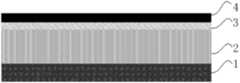
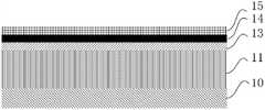
如图1所示,在N型硅衬底1上(N sub)生长一层N型硅外延层2(N Epi)。As shown in Figure 1, a layer of N-type silicon epitaxial layer 2 (N Epi) is grown on an N-type silicon substrate 1 (N sub).
如图2所示,在N型硅半导体外延层2上生长一层用作绝缘层的栅氧化层3,该氧化层为二氧化硅(SiO2),然后在该栅氧化层3上生长一层用作栅极的多晶硅4。As shown in Figure 2, a
利用光刻工艺在所述多晶硅层4上制作一个多晶硅窗口图形,然后通过刻蚀多晶硅得到如图3所示的多晶硅窗口5。A polysilicon window pattern is fabricated on the
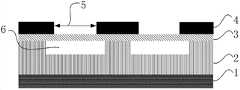
利用多晶硅窗口5做阻挡,在N型硅半导体外延层2上进行离子注入,形成如图4所示的p型体区(P Body)6。Using the
在多晶硅窗口5处采用光刻工艺制作源区(SRC)图形,如图5所示,利用光刻胶(PR)7做阻挡,在p型体区6中进行源区(SRC)的注入,形成源区(SRC)8,图5中有4个源区(SRC)8。At the
如图6所示,利用光刻工艺制作出接触孔(CONT)层形,再刻蚀出接触孔9。As shown in FIG. 6 , a contact hole (CONT) layer is fabricated by using a photolithography process, and then a
上述制作DMOS器件工艺流程中,在分别制作体区(BODY)、源区(SRC)和接触孔(CONT)的过程中,都采用了光刻和刻蚀工艺,导致平面型DMOS器件的制作工艺较复杂。并且,在制作体区(BODY)、源区(SRC)和接触孔(CONT)的过程中,每次使用的光刻技术都要确保多晶硅窗口处的光刻胶7的位置不能太偏,由于光刻对准本身有一定的套准偏差,多晶硅的窗口至少要保持一定的宽度,并且光刻胶7的宽度也不能太窄,因此以上工艺都限制了多晶硅窗口尺寸的进一步减小,导致DMOS器件内元胞的集成度较低,进而使得DMOS器件的性能较低。In the above-mentioned manufacturing process of DMOS devices, photolithography and etching processes are used in the process of respectively manufacturing the body region (BODY), source region (SRC) and contact hole (CONT), resulting in the manufacturing process of planar DMOS devices more complicated. Moreover, in the process of making the body region (BODY), the source region (SRC) and the contact hole (CONT), the photolithography technology used each time must ensure that the position of the
发明内容Contents of the invention
本发明实施例提供了一种DMOS器件及其制作方法,用以简化DMOS器件的制作工艺流程。Embodiments of the present invention provide a DMOS device and a manufacturing method thereof, which are used to simplify the manufacturing process of the DMOS device.
本发明实施例提供的一种DMOS器件的制作方法包括:A method for manufacturing a DMOS device provided in an embodiment of the present invention includes:
在生成了N型硅半导体衬底、N型硅半导体外延层、栅氧化层及多晶硅层之后,在多晶硅层上生长第一介质层,通过光刻及刻蚀将多晶硅层和第一介质层形成凹槽,露出栅氧化层;After the N-type silicon semiconductor substrate, N-type silicon semiconductor epitaxial layer, gate oxide layer and polysilicon layer are formed, the first dielectric layer is grown on the polysilicon layer, and the polysilicon layer and the first dielectric layer are formed by photolithography and etching. Grooves exposing the gate oxide layer;
通过所述凹槽将P型体区注入N型硅半导体外延层,并对P型体区进行驱入;Implanting the P-type body region into the N-type silicon semiconductor epitaxial layer through the groove, and driving the P-type body region;
通过所述凹槽将N型源区注入P型体区中。The N-type source region is injected into the P-type body region through the groove.
本发明实施例提供的一种DMOS器件,该DMOS器件采用上述制作方法制作而成。A DMOS device provided by an embodiment of the present invention is manufactured by using the above manufacturing method.
本发明实施例,在生成了N型硅半导体衬底、N型硅半导体外延层、栅氧化层及多晶硅层之后,在多晶硅层上生长第一介质层,通过光刻及刻蚀将多晶硅层和第一介质层形成凹槽,露出栅氧化层;通过所述凹槽将P型体区注入N型硅半导体外延层,并对P型体区进行驱入;通过所述凹槽将N型源区注入P型体区中,从而在形成N型源区的过程中避免了采用光刻及刻蚀的过程,简化了DMOS器件的制作流程。In the embodiment of the present invention, after the N-type silicon semiconductor substrate, the N-type silicon semiconductor epitaxial layer, the gate oxide layer, and the polysilicon layer are formed, a first dielectric layer is grown on the polysilicon layer, and the polysilicon layer and the polysilicon layer are formed by photolithography and etching. The first dielectric layer forms a groove to expose the gate oxide layer; inject the P-type body region into the N-type silicon semiconductor epitaxial layer through the groove, and drive the P-type body region; The region is implanted into the P-type body region, thereby avoiding the process of photolithography and etching in the process of forming the N-type source region, and simplifying the manufacturing process of the DMOS device.
附图说明Description of drawings
图1为现有技术在硅衬底上生长了外延层时的平面型DMOS器件剖面图;1 is a sectional view of a planar DMOS device when an epitaxial layer is grown on a silicon substrate in the prior art;
图2为现有技术在外延层上生长了绝缘层和多晶硅时的平面型DMOS器件剖面图;2 is a cross-sectional view of a planar DMOS device when an insulating layer and polysilicon are grown on an epitaxial layer in the prior art;
图3为现有技术具有多晶硅窗口的平面型DMOS器件剖面图;3 is a sectional view of a planar DMOS device with a polysilicon window in the prior art;
图4为现有技术具有p型体区的平面型DMOS器件剖面图;4 is a cross-sectional view of a planar DMOS device with a p-type body region in the prior art;
图5为现有技术具有源区的平面型DMOS器件剖面图;5 is a cross-sectional view of a planar DMOS device with a source region in the prior art;
图6为现有技术具有接触孔的平面型DMOS器件剖面图;6 is a cross-sectional view of a planar DMOS device with contact holes in the prior art;
图7为本发明实施例提供的DMOS器件的制作方法的流程图;FIG. 7 is a flowchart of a method for manufacturing a DMOS device provided by an embodiment of the present invention;
图8为本发明实施例提供的硅衬底上生长了外延层的平面型DMOS器件剖面图;8 is a cross-sectional view of a planar DMOS device with an epitaxial layer grown on a silicon substrate provided by an embodiment of the present invention;
图9为本发明实施例提供的外延层上生长了氧化层的平面型DMOS器件剖面图;9 is a cross-sectional view of a planar DMOS device with an oxide layer grown on the epitaxial layer provided by an embodiment of the present invention;
图10为本发明实施例提供的生长了多晶硅的平面型DMOS器件剖面图;10 is a cross-sectional view of a planar DMOS device grown with polysilicon provided by an embodiment of the present invention;
图11为本发明实施例提供的多晶硅上生长了第一介质层的平面型DMOS器件剖面图;11 is a cross-sectional view of a planar DMOS device with a first dielectric layer grown on polysilicon provided by an embodiment of the present invention;
图12为本发明实施例提供的具有多晶硅窗口的平面型DMOS器件剖面图;12 is a cross-sectional view of a planar DMOS device with a polysilicon window provided by an embodiment of the present invention;
图13为本发明实施例提供的具有p型体区的平面型DMOS器件剖面图;13 is a cross-sectional view of a planar DMOS device with a p-type body region provided by an embodiment of the present invention;
图14为本发明实施例提供的p型体区驱入后的平面型DMOS器件剖面图;FIG. 14 is a cross-sectional view of a planar DMOS device after the p-type body region is driven in according to an embodiment of the present invention;
图15为本发明实施例提供的具有源区的平面型DMOS器件剖面图;15 is a cross-sectional view of a planar DMOS device with a source region provided by an embodiment of the present invention;
图16为本发明实施例提供的生长了氮化硅后的平面型DMOS器件剖面图;16 is a cross-sectional view of a planar DMOS device after growing silicon nitride provided by an embodiment of the present invention;
图17为本发明实施例提供的具有深体区的平面型DMOS器件剖面图;17 is a cross-sectional view of a planar DMOS device with a deep body region provided by an embodiment of the present invention;
图18为本发明实施例提供的在氮化硅上生长了第二介质层的平面型DMOS器件剖面图;18 is a cross-sectional view of a planar DMOS device with a second dielectric layer grown on silicon nitride provided by an embodiment of the present invention;
图19为本发明实施例提供的在氮化硅侧壁形成侧墙后的平面型DMOS器件剖面图;FIG. 19 is a cross-sectional view of a planar DMOS device provided by an embodiment of the present invention after sidewalls are formed on silicon nitride sidewalls;
图20为本发明实施例提供的源区内具有p型重掺杂区的平面型DMOS器件剖面图;20 is a cross-sectional view of a planar DMOS device with a p-type heavily doped region in the source region provided by an embodiment of the present invention;
图21为本发明实施例提供的具有制作出接触孔的平面型DMOS器件剖面图;21 is a cross-sectional view of a planar DMOS device with contact holes provided by an embodiment of the present invention;
图22为本发明实施例提供的生长有用于连接源极的金属层的平面型DMOS器件剖面图;FIG. 22 is a cross-sectional view of a planar DMOS device provided with a metal layer used to connect to a source provided by an embodiment of the present invention;
图23为本发明实施例提供的晶背生长有金属层的平面型DMOS器件剖面图。FIG. 23 is a cross-sectional view of a planar DMOS device with a metal layer grown on the crystal back provided by an embodiment of the present invention.
具体实施方式Detailed ways
本发明实施例提供了一种DMOS器件及其制作方法,用以简化DMOS器件的制作工艺流程,减小DMOS器件多晶硅窗口尺寸,提高DMOS器件片内元胞的集成度,进而提高DMOS器件的性能。The embodiment of the present invention provides a DMOS device and a manufacturing method thereof, which are used to simplify the manufacturing process flow of the DMOS device, reduce the size of the polysilicon window of the DMOS device, improve the integration degree of cells in the DMOS device chip, and further improve the performance of the DMOS device. .
本发明实施例多次使用氧化层及氮化硅层刻蚀后形成的侧墙的阻挡作用,采用自对准注入方式,实现了在制作平面型DMOS器件的工艺流程中,省去了在元胞内制作体区、源区、深体区和接触孔的光刻和刻蚀过程,使得在完成同样平面型DMOS器件结构的前提下,简化了制作平面型DMOS器件的工艺流程,提高了芯片内元胞的集成度,降低了DMOS器件的制作成本。The embodiment of the present invention uses the blocking effect of the sidewall formed after the etching of the oxide layer and the silicon nitride layer for many times, adopts the self-aligned implantation method, and realizes that in the process flow of manufacturing the planar DMOS device, the element The photolithography and etching process of making the body region, source region, deep body region and contact hole in the cell simplifies the process flow of making planar DMOS devices and improves the chip efficiency while completing the same planar DMOS device structure. The integration degree of the inner cell reduces the manufacturing cost of the DMOS device.
本发明实施例提供的技术方案,可以适用于平面型DMOS器件的制作。The technical solutions provided by the embodiments of the present invention can be applied to the manufacture of planar DMOS devices.
以下将结合附图对本发明实施例提供的技术方案进行详细的描述。The technical solutions provided by the embodiments of the present invention will be described in detail below in conjunction with the accompanying drawings.
参见图7,本发明实施例提供的一种DMOS器件的制作方法,包括步骤:Referring to FIG. 7, a method for manufacturing a DMOS device provided by an embodiment of the present invention includes steps:
S101、在生成了N型硅半导体衬底、N型硅半导体外延层、栅氧化层及多晶硅层之后,在多晶硅层上生长第一介质层,通过光刻及刻蚀将多晶硅层和第一介质层形成凹槽,露出栅氧化层;S101. After forming the N-type silicon semiconductor substrate, the N-type silicon semiconductor epitaxial layer, the gate oxide layer and the polysilicon layer, grow the first dielectric layer on the polysilicon layer, and combine the polysilicon layer and the first dielectric layer by photolithography and etching The layer forms a groove, exposing the gate oxide layer;
S102、通过所述凹槽将P型体区注入N型硅半导体外延层,并对P型体区进行驱入;S102, implanting the P-type body region into the N-type silicon semiconductor epitaxial layer through the groove, and driving the P-type body region;
S103、通过所述凹槽将N型源区注入P型体区中。S103, injecting the N-type source region into the P-type body region through the groove.
较佳地,通过所述凹槽将N型源区注入P型体区中之后,该方法还包括:Preferably, after injecting the N-type source region into the P-type body region through the groove, the method further includes:
生长氮化硅层,该氮化硅层在所述凹槽的多晶硅层和第一介质层的侧壁形成第一侧墙;growing a silicon nitride layer, the silicon nitride layer forms a first sidewall on the sidewalls of the polysilicon layer and the first dielectric layer in the groove;
通过形成有第一侧墙的凹槽,注入深体区。The deep body region is injected through the recess formed with the first sidewall.
较佳地,注入深体区之后,该方法还包括:Preferably, after injecting into the deep body region, the method further includes:
积淀第二介质层,该第二介质层在凹槽的第一侧墙上形成第二侧墙;depositing a second dielectric layer forming second sidewalls on the first sidewalls of the recess;
对第二介质层进行刻蚀,保留在凹槽的第一侧墙上形成的第二侧墙;Etching the second dielectric layer, retaining the second sidewall formed on the first sidewall of the groove;
通过形成有第二侧墙的凹槽,在N型源区中注入P型重掺杂;Implanting P-type heavy doping into the N-type source region through the groove formed with the second sidewall;
将所述第二侧墙腐蚀掉。The second sidewall is etched away.
较佳地,将所述第二侧墙腐蚀掉之后,该方法还包括:Preferably, after the second side wall is etched away, the method further includes:
对氮化硅层进行刻蚀,保留所述第一侧墙,露出N型源区和P型重掺杂。Etching the silicon nitride layer, retaining the first sidewall, exposing the N-type source region and the P-type heavily doped.
较佳地,露出N型源区和P型重掺杂之后,该方法还包括:Preferably, after exposing the N-type source region and P-type heavy doping, the method further includes:
生长第一金属层,使得DMOS器件的源极和栅极的电性链接;growing the first metal layer to electrically connect the source and gate of the DMOS device;
通过生长第二金属层,形成DMOS器件的漏极。By growing the second metal layer, the drain of the DMOS device is formed.
下面结合DMOS器件结构剖面图给出具体的制作流程介绍。The following is a detailed description of the manufacturing process combined with the structure cross-sectional view of the DMOS device.
本发明实施例提供的一种平面型DMOS器件的制作方法,具体包括:A method for manufacturing a planar DMOS device provided in an embodiment of the present invention specifically includes:
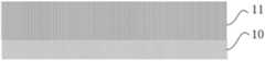
参见图8,在N型硅半导体衬底(N sub)10上生长一层N型硅半导体外延层(N Epi)11。Referring to FIG. 8, a layer of N-type silicon semiconductor epitaxial layer (N Epi) 11 is grown on N-type silicon semiconductor substrate (N sub) 10.
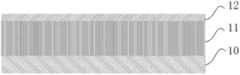
参见图9,采用热氧化方法在所述N型硅半导体外延层(N Epi)11上生长一层厚度为1500埃
采用氢氟酸(HF溶液)剥除掉初始氧化层12,目的是为了保证硅片表面的清洁,此时的DMOS器件结构剖面图如图8所示。The
参见图10,采用热氧化的方式在表面非常干净的外延层11上生长一层厚度在500~

参见图11,将图10所示的DMOS器件放置的在炉管中或者化学气相沉积(Chemical Vapor Deposition,CVD)机台中淀积一层厚度为
淀积该第一介质层15的目的是为了后续在刻蚀氮化硅层时,保证N型源区(N SRC)表面的氮化硅刻蚀掉的同时,多晶硅层表面不露出来,即使得多晶硅(POLY)14与N型源区绝缘,此时的DMOS器件结构的剖面图如图11所示。The purpose of depositing the
参见图12,利用传统的光刻方法在第一介质层15上刻出体区(BODY)的窗口图形,然后采用含氟(F)的气体对第一介质层15上的体区窗口图形进行干法刻蚀,刻蚀出一个以第一介质层15为台阶的窗口,然后采用含氯(Cl)的气体对第一介质层15下面的多晶硅(POLY)14层进行刻蚀,最后刻蚀出如图12所示的以第一介质层15和多晶硅层14为台阶的窗口(即所述的凹槽)20。Referring to FIG. 12, the window pattern of the body region (BODY) is etched on the
参见图13,以第一介质层15和多晶硅14(POLY)形成的窗口20做屏蔽,对窗口20下的N型硅外延层(N Epi)11进行自对准方式的离子注入,注入的离子可以为正三价离子,如B3+,此时在外延层(N Epi)11上通过自对准方式注入的离子形成的区域为如图13所示的DMOS器件的体区(BODY)21,该体区(BODY)21为p型体区(P BODY)。13, the
只有在窗口20的外延层(N Epi)11区域才可以注入离子,其余外延层部分被第一介质层15以及多晶硅(POLY)14阻挡。所述外延层中离子的注入深度,即p型体区的深度,可以根据P型体区的结深而决定,注入离子的深度可以在1μm左右。Ions can be implanted only in the epitaxial layer (NEpi) 11 region of the
将图13所示的具有p型体区21的DMOS器件放置在温度约为1100℃的炉管中,进行p型体区中离子的进一步驱入,使得在p型体区(BODY)21中注入的离子分布均匀,参见图14,形成新的p型体区(BODY)22。Place the DMOS device with the p-type body region 21 shown in FIG. 13 in a furnace tube at a temperature of about 1100° C. to further drive ions in the p-type body region, so that in the p-type body region (BODY) 21 The implanted ions are evenly distributed, as shown in FIG. 14 , and a new p-type body region (BODY) 22 is formed.
参见图15,利用第一介质层15和多晶硅(POLY)14形成的窗口20做屏蔽,在P型体区(BODY)22中进行自对准方式的离子注入,该离子可以为正五价的杂质离子,如P5+。此时在P型体区(BODY)22中注入的离子形成的区域为DMOS器件的N型源区(N SRC)23。Referring to FIG. 15 , using the
同理,由于第一介质层15以及多晶硅(POLY)14的阻挡,只有在窗口20的外延层区域可以注入离子,此次注入离子的深度,即N型源区23的深度,根据N型源区23的结深而决定,深度约在1μm左右。Similarly, due to the barriers of the
参见图16,将图15所示的DMOS器件放置在炉管中生长一层厚度约


参见图17,利用侧墙24,采用自对准方式对p型体区22进行离子注入,在p型体区22和外延层11之间形成如图17所示的深体区(DEEP BODY)25,离子注入的深度约在1μm左右,即深体区25的深度为1μm左右,此步骤形成深体区25的目的是为了提高非嵌位感性开关(Unclamped Inductive Switching,UIS)的能力。Referring to FIG. 17 , using the
参见图18,将图17所示的DMOS器件放置在炉管中或者CVD机台中淀积一层厚度约的介质层(TEOS),此介质层(TEOS)的制备工艺和第一介质层15的制备工艺一致,所形成的介质层(TEOS)为DMOS器件的第二介质层17,此时的DMOS器件结构的剖面图如图18所示。Referring to Fig. 18, place the DMOS device shown in Fig. 17 in a furnace tube or in a CVD machine to deposit a layer with a thickness of about The dielectric layer (TEOS), the preparation process of this dielectric layer (TEOS) is consistent with the preparation process of the
利用第二介质层17在氮化硅16的侧壁形成的侧墙(第二侧墙)26,采用自对准方式在DMOS器件的N型源区(SRC)23中注入P型重掺杂(P+)离子,形成如图19所示的P型重掺杂区域27。Using the sidewall (second sidewall) 26 formed on the sidewall of the
该P型重掺杂离子的浓度要高于N型源区23中的N型源(N SRC)的浓度,目的是要使得此次所注入的P型重掺杂区域27的导电类型由原来的N型变成P型,该P型重掺杂区域27的作用是使得原来的N型源区23变成两个源区。The concentration of the P-type heavily doped ions is higher than the concentration of the N-type source (NSRC) in the N-
另外,也可以先将氮化硅层16之上的第二介质层17刻蚀掉,仅保留第二侧墙26,然后再采用自对准方式在DMOS器件的N型源区23中注入P型重掺杂(P+)离子,形成P型重掺杂区域27。In addition, the
将图19所示的DMOS器件放置在氢氟酸液中腐蚀掉氮化硅16,形成如图20所示的DMOS器件结构。The DMOS device shown in FIG. 19 is placed in hydrofluoric acid solution to etch away the
对覆盖于第一介质层(TEOS)15上的氮化硅层16进行干法刻蚀,参见图21,在多晶硅(POLY)14和第一介质层15的侧壁留有氮化硅材质的侧墙(即所述的第一侧墙)28,同时将多晶硅(POLY)14和第一介质层15窗口之间的硅衬底表面露出来,即将N型源区23的接触孔29露出来。Carry out dry etching to the
此时,在没有经过传统器件制作工艺的光刻步骤的情况下,本发明实施例就已经把需要的源极接触孔29的位置做好了,简化了工艺流程。此时的DMOS器件结构剖面图如图21所示。At this time, without going through the photolithography step of the traditional device manufacturing process, the embodiment of the present invention has already prepared the required position of the
其中,一个侧墙28、一个源极(即N型源区)23和一个作为栅极的多晶硅14,即构成一个DMOS器件基本组成单元的元胞,多晶硅的窗口尺寸决定了元胞的大小,决定了元胞在芯片上的密度,从而决定了元胞的集成度。Wherein, a
参见图21,由于源区之间的深体区注入区域的水平宽度很小,在不考虑该源区之间深体区注入区域的水平宽度的情况下,本发明多晶硅的窗口尺寸至少为:2*氮化硅侧墙28的水平厚度+2*第二介质层17的侧墙的水平厚度,其中氮化硅侧墙28的水平厚度即为氮化硅层的厚度

传统制作工艺多晶硅的窗口尺寸考虑到光刻工艺中光刻机的分辨率(0.5μm)和套准精度(0.15μm),如果源区的最小宽度为0.5μm,则多晶硅的窗口尺寸至少为:2*0.5μm+2*0.15μm+0.5=0.7μm=1.8μm。The window size of polysilicon in the traditional manufacturing process takes into account the resolution (0.5 μm) and registration accuracy (0.15 μm) of the lithography machine in the lithography process. If the minimum width of the source region is 0.5 μm, the window size of polysilicon is at least: 2*0.5 μm+2*0.15 μm+0.5=0.7 μm=1.8 μm.
本发明DMOS器件的制作方法得到的多晶硅开窗尺寸至少减小了1.1μm,并且多晶硅窗口所用的面积也相应减小。元胞密度定义为:多晶硅开窗尺寸+多晶硅线条宽度,对于分辨率为0.5μm光刻机,多晶硅线条宽度最小值为0.5μm。所以,本发明优化后的元胞密度为0.7μm+0.5μm=1.2μm,传统制作工艺得到的元胞密度为1.8μm+0.5μm=2.3μm,可以得到,本发明器件制作工艺优化后的元胞密度提高率为47.8%((2.3-1.2)/2.3=47.8%)。The size of the polysilicon window obtained by the manufacturing method of the DMOS device of the present invention is reduced by at least 1.1 μm, and the area used by the polysilicon window is correspondingly reduced. Cell density is defined as: polysilicon window size + polysilicon line width, for a lithography machine with a resolution of 0.5 μm, the minimum polysilicon line width is 0.5 μm. Therefore, the optimized cell density of the present invention is 0.7 μm + 0.5 μm = 1.2 μm, and the cell density obtained by the traditional manufacturing process is 1.8 μm + 0.5 μm = 2.3 μm, which can be obtained. The increase rate of cell density was 47.8% ((2.3-1.2)/2.3=47.8%).
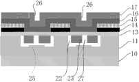
参见图22,采用溅射的方式在整个MOS器件上生长一层厚度约3~4μm的金属层(第一金属层)18,然后利用刻蚀的方法,将分别接触栅极和接触源极的金属层分开,使得源极和栅极保持绝缘,以便进行源极和栅极的电性链接,该金属18的材料可以为铝硅铜(AlSiCu)合金,此时制作好的DMOS器件结构剖面图如图22所示。Referring to FIG. 22 , a metal layer (first metal layer) 18 with a thickness of about 3-4 μm is grown on the entire MOS device by sputtering, and then the metal layer (first metal layer) 18 that is in contact with the gate and the source is respectively etched by etching. The metal layer is separated so that the source and the gate are kept insulated so as to electrically connect the source and the gate. The material of the
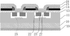
参见图23,将DMOS器件的背部的硅晶片减薄到300μm厚,然后采用溅射或者蒸镀的方式在所述减薄后的DMOS器件的背面先后生长三层不同材料的金属层(第二金属层),作为DMOS器件的晶背19,所述三层金属层的材料分别可以为钛(Ti)、镍(Ni)、银(Ag),其中,最先镀到DMOS器件背面的金属层的材料为Ti,其次为Ni,最后为Ag。此时形成的晶背19即为DMOS器件的漏极,最终制作好的DMOS器件结构剖面图如图23所示。Referring to FIG. 23 , the silicon wafer on the back of the DMOS device is thinned to a thickness of 300 μm, and then three layers of metal layers of different materials are successively grown on the back of the thinned DMOS device by sputtering or vapor deposition (the second Metal layer), as the crystal back 19 of the DMOS device, the materials of the three metal layers can be titanium (Ti), nickel (Ni), silver (Ag) respectively, wherein, the metal layer plated to the back of the DMOS device first The primary material is Ti, followed by Ni, and finally Ag. The crystal back 19 formed at this time is the drain of the DMOS device, and the structure cross-sectional view of the finally fabricated DMOS device is shown in FIG. 23 .
综上所述,本发明实施例提供的一种DMOS器件及其制作方法,在DMOS器件的制作过程中,多次使用了氧化层/氮化硅层刻蚀后形成的侧墙(SPACER)的阻挡作用,实现了体区(BODY)、源区(SRC)和深体区(DEEP BODY)的自对准注入,同时也省去在元胞内进行接触孔的光刻和刻蚀的步骤,使得在完成同样器件结构的前提下,省去了在元胞内制作体区(BODY)、源区(SRC)和深体区(DEEP BODY)的光刻和刻蚀过程,简化了制作DMOS器件的工艺流程,降低了芯片的制作成本。To sum up, in the DMOS device and its manufacturing method provided by the embodiment of the present invention, in the manufacturing process of the DMOS device, the spacer (SPACER) formed after the oxide layer/silicon nitride layer is etched is used multiple times. The blocking effect realizes the self-aligned implantation of the body region (BODY), the source region (SRC) and the deep body region (DEEP BODY), and also saves the steps of photolithography and etching of the contact hole in the cell, Under the premise of completing the same device structure, the photolithography and etching process of making the body region (BODY), source region (SRC) and deep body region (DEEP BODY) in the cell is omitted, which simplifies the manufacture of DMOS devices The technological process reduces the production cost of the chip.
同时,本发明平面型DMOS器件制作工艺减小了单个元胞的尺寸,优化后的元胞密度提高率为47.8%,提高了芯片内元胞集成度,降低了芯片的制作成本。At the same time, the manufacturing process of the planar DMOS device of the present invention reduces the size of a single cell, and the optimized cell density increase rate is 47.8%, which improves the integration of cells in the chip and reduces the manufacturing cost of the chip.
显然,本领域的技术人员可以对本发明进行各种改动和变型而不脱离本发明的精神和范围。这样,倘若本发明的这些修改和变型属于本发明权利要求及其等同技术的范围之内,则本发明也意图包含这些改动和变型在内。Obviously, those skilled in the art can make various changes and modifications to the present invention without departing from the spirit and scope of the present invention. Thus, if these modifications and variations of the present invention fall within the scope of the claims of the present invention and their equivalent technologies, the present invention also intends to include these modifications and variations.
Claims (10)

Priority Applications (1)
| Application Number | Priority Date | Filing Date | Title |
|---|---|---|---|
| CN201110312583.8ACN103050405B (en) | 2011-10-14 | 2011-10-14 | DMOS (double-diffused metal oxide semiconductor) device and manufacturing method thereof |
Applications Claiming Priority (1)
| Application Number | Priority Date | Filing Date | Title |
|---|---|---|---|
| CN201110312583.8ACN103050405B (en) | 2011-10-14 | 2011-10-14 | DMOS (double-diffused metal oxide semiconductor) device and manufacturing method thereof |
Publications (2)
| Publication Number | Publication Date |
|---|---|
| CN103050405Atrue CN103050405A (en) | 2013-04-17 |
| CN103050405B CN103050405B (en) | 2015-06-03 |
Family
ID=48063005
Family Applications (1)
| Application Number | Title | Priority Date | Filing Date |
|---|---|---|---|
| CN201110312583.8AExpired - Fee RelatedCN103050405B (en) | 2011-10-14 | 2011-10-14 | DMOS (double-diffused metal oxide semiconductor) device and manufacturing method thereof |
Country Status (1)
| Country | Link |
|---|---|
| CN (1) | CN103050405B (en) |
Cited By (6)
| Publication number | Priority date | Publication date | Assignee | Title |
|---|---|---|---|---|
| CN104795440A (en)* | 2014-01-17 | 2015-07-22 | 北大方正集团有限公司 | VDMOS (Vertical double-diffused metal oxide semiconductor) and manufacturing method thereof |
| CN104810287A (en)* | 2014-01-26 | 2015-07-29 | 北大方正集团有限公司 | Double-diffusion metal oxide transistor manufacture method and transistor device |
| CN106298482A (en)* | 2015-05-29 | 2017-01-04 | 中芯国际集成电路制造(上海)有限公司 | The forming method of semiconductor structure |
| CN106328524A (en)* | 2015-06-15 | 2017-01-11 | 北大方正集团有限公司 | Manufacturing method of vertical double-diffused MOS device |
| CN113707545A (en)* | 2021-08-18 | 2021-11-26 | 深圳市美浦森半导体有限公司 | Method and device for improving avalanche characteristic of MOSFET (Metal-oxide-semiconductor field Effect transistor) |
| CN117637607A (en)* | 2024-01-24 | 2024-03-01 | 北京智芯微电子科技有限公司 | Method for forming self-aligned contact groove of super-junction semiconductor and super-junction semiconductor structure |
Citations (3)
| Publication number | Priority date | Publication date | Assignee | Title |
|---|---|---|---|---|
| US20040018705A1 (en)* | 2002-04-11 | 2004-01-29 | Colson Paul Frans Marie | Semiconductor structure and method for processing such a structure |
| CN101383287A (en)* | 2008-09-27 | 2009-03-11 | 电子科技大学 | A method of manufacturing a vertical double-diffused metal oxide semiconductor device |
| CN101399227A (en)* | 2007-09-26 | 2009-04-01 | 中国科学院微电子研究所 | Fabrication method of fully self-aligned strip gate power vertical double diffused field effect transistor |
- 2011
- 2011-10-14CNCN201110312583.8Apatent/CN103050405B/ennot_activeExpired - Fee Related
Patent Citations (3)
| Publication number | Priority date | Publication date | Assignee | Title |
|---|---|---|---|---|
| US20040018705A1 (en)* | 2002-04-11 | 2004-01-29 | Colson Paul Frans Marie | Semiconductor structure and method for processing such a structure |
| CN101399227A (en)* | 2007-09-26 | 2009-04-01 | 中国科学院微电子研究所 | Fabrication method of fully self-aligned strip gate power vertical double diffused field effect transistor |
| CN101383287A (en)* | 2008-09-27 | 2009-03-11 | 电子科技大学 | A method of manufacturing a vertical double-diffused metal oxide semiconductor device |
Cited By (8)
| Publication number | Priority date | Publication date | Assignee | Title |
|---|---|---|---|---|
| CN104795440A (en)* | 2014-01-17 | 2015-07-22 | 北大方正集团有限公司 | VDMOS (Vertical double-diffused metal oxide semiconductor) and manufacturing method thereof |
| CN104795440B (en)* | 2014-01-17 | 2018-09-25 | 北大方正集团有限公司 | A kind of VDMOS and preparation method thereof |
| CN104810287A (en)* | 2014-01-26 | 2015-07-29 | 北大方正集团有限公司 | Double-diffusion metal oxide transistor manufacture method and transistor device |
| CN104810287B (en)* | 2014-01-26 | 2019-04-26 | 北大方正集团有限公司 | Fabrication method of double diffused metal oxide transistor and transistor device |
| CN106298482A (en)* | 2015-05-29 | 2017-01-04 | 中芯国际集成电路制造(上海)有限公司 | The forming method of semiconductor structure |
| CN106328524A (en)* | 2015-06-15 | 2017-01-11 | 北大方正集团有限公司 | Manufacturing method of vertical double-diffused MOS device |
| CN113707545A (en)* | 2021-08-18 | 2021-11-26 | 深圳市美浦森半导体有限公司 | Method and device for improving avalanche characteristic of MOSFET (Metal-oxide-semiconductor field Effect transistor) |
| CN117637607A (en)* | 2024-01-24 | 2024-03-01 | 北京智芯微电子科技有限公司 | Method for forming self-aligned contact groove of super-junction semiconductor and super-junction semiconductor structure |
Also Published As
| Publication number | Publication date |
|---|---|
| CN103050405B (en) | 2015-06-03 |
Similar Documents
| Publication | Publication Date | Title |
|---|---|---|
| TWI446416B (en) | High-density trench MOS field-effect transistor with single mask predetermined gate trench and contact trench | |
| JP5551213B2 (en) | Manufacturing method of semiconductor device | |
| US7842574B2 (en) | Method of manufacturing a semiconductor power device | |
| CN103050405B (en) | DMOS (double-diffused metal oxide semiconductor) device and manufacturing method thereof | |
| CN104716177B (en) | A kind of manufacture method for the radio frequency LDMOS device for improving electric leakage | |
| CN104282645A (en) | trench type power semiconductor device and manufacturing method thereof | |
| KR101832334B1 (en) | Semiconductor device and method for fabricating the same | |
| CN109216276B (en) | MOS (Metal oxide semiconductor) tube and manufacturing method thereof | |
| CN105529256B (en) | Semiconductor devices and the method for manufacturing semiconductor devices using alignment layer | |
| CN111755525A (en) | A Trench MOS power device and preparation method thereof | |
| CN113053738A (en) | Split gate type groove MOS device and preparation method thereof | |
| CN113517350A (en) | A low-voltage shielded gate MOSFET device and its manufacturing method | |
| CN108649072A (en) | A kind of groove MOSFET device and its manufacturing method of low on-resistance | |
| CN109755322A (en) | Silicon carbide MOSFET device and preparation method thereof | |
| CN110223959A (en) | The Metal Oxide Semiconductor Field Effect Transistor and preparation method thereof of depth groove | |
| CN104241356B (en) | DMOS device and manufacturing method thereof | |
| TWI524524B (en) | Method and structure of power semiconductor components | |
| CN115000154B (en) | A silicon carbide MOSFET device with an L-shaped vertical source and a manufacturing method thereof | |
| CN103872095B (en) | The groove of p-type LDMOS device and process | |
| CN113921401B (en) | A new type of superjunction and SGT composite MOSFET and its manufacturing method | |
| JP2005516381A (en) | Method for forming narrow trenches in a semiconductor substrate | |
| CN106783606A (en) | Power semiconductor and preparation method thereof | |
| CN111933700B (en) | Power semiconductor device and method for manufacturing the same | |
| CN111987165B (en) | Method for manufacturing lateral double-diffused transistor | |
| CN115312601A (en) | MOSFET device and preparation method thereof |
Legal Events
| Date | Code | Title | Description |
|---|---|---|---|
| C06 | Publication | ||
| PB01 | Publication | ||
| C10 | Entry into substantive examination | ||
| SE01 | Entry into force of request for substantive examination | ||
| C14 | Grant of patent or utility model | ||
| GR01 | Patent grant | ||
| TR01 | Transfer of patent right | ||
| TR01 | Transfer of patent right | Effective date of registration:20220726 Address after:518116 founder Microelectronics Industrial Park, No. 5, Baolong seventh Road, Baolong Industrial City, Longgang District, Shenzhen, Guangdong Province Patentee after:SHENZHEN FOUNDER MICROELECTRONICS Co.,Ltd. Address before:100871, Beijing, Haidian District Cheng Fu Road 298, founder building, 9 floor Patentee before:PEKING UNIVERSITY FOUNDER GROUP Co.,Ltd. Patentee before:SHENZHEN FOUNDER MICROELECTRONICS Co.,Ltd. | |
| CF01 | Termination of patent right due to non-payment of annual fee | ||
| CF01 | Termination of patent right due to non-payment of annual fee | Granted publication date:20150603 |