CN103035527A - Nitrogen passivation of source and drain recesses - Google Patents
Nitrogen passivation of source and drain recessesDownload PDFInfo
- Publication number
- CN103035527A CN103035527ACN2012100408628ACN201210040862ACN103035527ACN 103035527 ACN103035527 ACN 103035527ACN 2012100408628 ACN2012100408628 ACN 2012100408628ACN 201210040862 ACN201210040862 ACN 201210040862ACN 103035527 ACN103035527 ACN 103035527A
- Authority
- CN
- China
- Prior art keywords
- substrate
- groove
- nitrogen
- source
- drain
- Prior art date
- Legal status (The legal status is an assumption and is not a legal conclusion. Google has not performed a legal analysis and makes no representation as to the accuracy of the status listed.)
- Granted
Links
- IJGRMHOSHXDMSA-UHFFFAOYSA-NAtomic nitrogenChemical compoundN#NIJGRMHOSHXDMSA-UHFFFAOYSA-N0.000titleclaimsabstractdescription160
- 229910052757nitrogenInorganic materials0.000titleclaimsabstractdescription80
- 238000002161passivationMethods0.000titleclaimsabstractdescription58
- 239000000758substrateSubstances0.000claimsabstractdescription126
- 238000000034methodMethods0.000claimsabstractdescription122
- 230000008569processEffects0.000claimsdescription89
- 239000004065semiconductorSubstances0.000claimsdescription50
- 229910000577Silicon-germaniumInorganic materials0.000claimsdescription26
- 239000002019doping agentSubstances0.000claimsdescription24
- ZOXJGFHDIHLPTG-UHFFFAOYSA-NBoronChemical compound[B]ZOXJGFHDIHLPTG-UHFFFAOYSA-N0.000claimsdescription16
- 229910052796boronInorganic materials0.000claimsdescription16
- 238000005530etchingMethods0.000claimsdescription16
- 238000000137annealingMethods0.000claimsdescription14
- 230000004888barrier functionEffects0.000claimsdescription14
- 239000007789gasSubstances0.000claimsdescription11
- QJGQUHMNIGDVPM-UHFFFAOYSA-Nnitrogen groupChemical group[N]QJGQUHMNIGDVPM-UHFFFAOYSA-N0.000claimsdescription10
- 230000015572biosynthetic processEffects0.000claimsdescription2
- 238000004519manufacturing processMethods0.000abstractdescription10
- 238000011049fillingMethods0.000abstractdescription4
- 239000010410layerSubstances0.000description123
- 239000000463materialSubstances0.000description30
- 125000006850spacer groupChemical group0.000description22
- LEVVHYCKPQWKOP-UHFFFAOYSA-N[Si].[Ge]Chemical compound[Si].[Ge]LEVVHYCKPQWKOP-UHFFFAOYSA-N0.000description19
- XUIMIQQOPSSXEZ-UHFFFAOYSA-NSiliconChemical compound[Si]XUIMIQQOPSSXEZ-UHFFFAOYSA-N0.000description18
- 229910052710siliconInorganic materials0.000description18
- 239000010703siliconSubstances0.000description18
- 229910052751metalInorganic materials0.000description16
- 239000002184metalSubstances0.000description16
- 230000006870functionEffects0.000description12
- 239000003989dielectric materialSubstances0.000description10
- OKTJSMMVPCPJKN-UHFFFAOYSA-NCarbonChemical compound[C]OKTJSMMVPCPJKN-UHFFFAOYSA-N0.000description9
- 229910052799carbonInorganic materials0.000description9
- VYPSYNLAJGMNEJ-UHFFFAOYSA-NSilicium dioxideChemical compoundO=[Si]=OVYPSYNLAJGMNEJ-UHFFFAOYSA-N0.000description8
- 229910052814silicon oxideInorganic materials0.000description8
- 238000002955isolationMethods0.000description7
- 229910021420polycrystalline siliconInorganic materials0.000description7
- 238000001039wet etchingMethods0.000description7
- 229910052581Si3N4Inorganic materials0.000description6
- 150000004767nitridesChemical class0.000description6
- 229920005591polysiliconPolymers0.000description6
- HQVNEWCFYHHQES-UHFFFAOYSA-Nsilicon nitrideChemical compoundN12[Si]34N5[Si]62N3[Si]51N64HQVNEWCFYHHQES-UHFFFAOYSA-N0.000description6
- 238000005229chemical vapour depositionMethods0.000description5
- 238000000151depositionMethods0.000description5
- 238000001312dry etchingMethods0.000description5
- 229910021332silicideInorganic materials0.000description5
- 230000008901benefitEffects0.000description4
- 230000005669field effectEffects0.000description4
- 238000012545processingMethods0.000description4
- FVBUAEGBCNSCDD-UHFFFAOYSA-Nsilicide(4-)Chemical compound[Si-4]FVBUAEGBCNSCDD-UHFFFAOYSA-N0.000description4
- WGTYBPLFGIVFAS-UHFFFAOYSA-Mtetramethylammonium hydroxideChemical compound[OH-].C[N+](C)(C)CWGTYBPLFGIVFAS-UHFFFAOYSA-M0.000description4
- RYGMFSIKBFXOCR-UHFFFAOYSA-NCopperChemical compound[Cu]RYGMFSIKBFXOCR-UHFFFAOYSA-N0.000description3
- 238000000231atomic layer depositionMethods0.000description3
- 239000010949copperSubstances0.000description3
- 229910052802copperInorganic materials0.000description3
- 238000013461designMethods0.000description3
- 239000007943implantSubstances0.000description3
- 238000002513implantationMethods0.000description3
- 230000001965increasing effectEffects0.000description3
- 238000005468ion implantationMethods0.000description3
- 229910044991metal oxideInorganic materials0.000description3
- 150000004706metal oxidesChemical class0.000description3
- 229920002120photoresistant polymerPolymers0.000description3
- KRHYYFGTRYWZRS-UHFFFAOYSA-NFluoraneChemical compoundFKRHYYFGTRYWZRS-UHFFFAOYSA-N0.000description2
- OAICVXFJPJFONN-UHFFFAOYSA-NPhosphorusChemical compound[P]OAICVXFJPJFONN-UHFFFAOYSA-N0.000description2
- GWEVSGVZZGPLCZ-UHFFFAOYSA-NTitan oxideChemical compoundO=[Ti]=OGWEVSGVZZGPLCZ-UHFFFAOYSA-N0.000description2
- MCMNRKCIXSYSNV-UHFFFAOYSA-NZirconium dioxideChemical compoundO=[Zr]=OMCMNRKCIXSYSNV-UHFFFAOYSA-N0.000description2
- 229910052787antimonyInorganic materials0.000description2
- WATWJIUSRGPENY-UHFFFAOYSA-Nantimony atomChemical compound[Sb]WATWJIUSRGPENY-UHFFFAOYSA-N0.000description2
- 229910052785arsenicInorganic materials0.000description2
- RQNWIZPPADIBDY-UHFFFAOYSA-Narsenic atomChemical compound[As]RQNWIZPPADIBDY-UHFFFAOYSA-N0.000description2
- 239000004020conductorSubstances0.000description2
- 238000005137deposition processMethods0.000description2
- 238000011161developmentMethods0.000description2
- 238000009792diffusion processMethods0.000description2
- 238000009826distributionMethods0.000description2
- 238000005516engineering processMethods0.000description2
- 238000000407epitaxyMethods0.000description2
- 238000011065in-situ storageMethods0.000description2
- 238000004518low pressure chemical vapour depositionMethods0.000description2
- 238000004377microelectronicMethods0.000description2
- 238000000059patterningMethods0.000description2
- 229910052698phosphorusInorganic materials0.000description2
- 239000011574phosphorusSubstances0.000description2
- 238000005240physical vapour depositionMethods0.000description2
- 238000005268plasma chemical vapour depositionMethods0.000description2
- 238000000623plasma-assisted chemical vapour depositionMethods0.000description2
- 238000005498polishingMethods0.000description2
- 229910010271silicon carbideInorganic materials0.000description2
- HBMJWWWQQXIZIP-UHFFFAOYSA-Nsilicon carbideChemical compound[Si+]#[C-]HBMJWWWQQXIZIP-UHFFFAOYSA-N0.000description2
- 239000000126substanceSubstances0.000description2
- WFKWXMTUELFFGS-UHFFFAOYSA-NtungstenChemical compound[W]WFKWXMTUELFFGS-UHFFFAOYSA-N0.000description2
- 239000010937tungstenSubstances0.000description2
- 229910052721tungstenInorganic materials0.000description2
- 238000000038ultrahigh vacuum chemical vapour depositionMethods0.000description2
- 238000000927vapour-phase epitaxyMethods0.000description2
- ITWBWJFEJCHKSN-UHFFFAOYSA-N1,4,7-triazonaneChemical compoundC1CNCCNCCN1ITWBWJFEJCHKSN-UHFFFAOYSA-N0.000description1
- 229910000980Aluminium gallium arsenideInorganic materials0.000description1
- JBRZTFJDHDCESZ-UHFFFAOYSA-NAsGaChemical compound[As]#[Ga]JBRZTFJDHDCESZ-UHFFFAOYSA-N0.000description1
- WKBOTKDWSSQWDR-UHFFFAOYSA-NBromine atomChemical compound[Br]WKBOTKDWSSQWDR-UHFFFAOYSA-N0.000description1
- ZAMOUSCENKQFHK-UHFFFAOYSA-NChlorine atomChemical compound[Cl]ZAMOUSCENKQFHK-UHFFFAOYSA-N0.000description1
- YCKRFDGAMUMZLT-UHFFFAOYSA-NFluorine atomChemical compound[F]YCKRFDGAMUMZLT-UHFFFAOYSA-N0.000description1
- 229910005540GaPInorganic materials0.000description1
- 229910001218Gallium arsenideInorganic materials0.000description1
- 229910004129HfSiOInorganic materials0.000description1
- 229910000673Indium arsenideInorganic materials0.000description1
- GPXJNWSHGFTCBW-UHFFFAOYSA-NIndium phosphideChemical compound[In]#PGPXJNWSHGFTCBW-UHFFFAOYSA-N0.000description1
- 229910010038TiAlInorganic materials0.000description1
- 229910010037TiAlNInorganic materials0.000description1
- ATJFFYVFTNAWJD-UHFFFAOYSA-NTinChemical compound[Sn]ATJFFYVFTNAWJD-UHFFFAOYSA-N0.000description1
- 229910045601alloyInorganic materials0.000description1
- 239000000956alloySubstances0.000description1
- 230000004075alterationEffects0.000description1
- 229910052782aluminiumInorganic materials0.000description1
- XAGFODPZIPBFFR-UHFFFAOYSA-NaluminiumChemical compound[Al]XAGFODPZIPBFFR-UHFFFAOYSA-N0.000description1
- PNEYBMLMFCGWSK-UHFFFAOYSA-Naluminium oxideInorganic materials[O-2].[O-2].[O-2].[Al+3].[Al+3]PNEYBMLMFCGWSK-UHFFFAOYSA-N0.000description1
- GDTBXPJZTBHREO-UHFFFAOYSA-NbromineSubstancesBrBrGDTBXPJZTBHREO-UHFFFAOYSA-N0.000description1
- 229910052794bromiumInorganic materials0.000description1
- 239000003990capacitorSubstances0.000description1
- 239000003795chemical substances by applicationSubstances0.000description1
- 229910052801chlorineInorganic materials0.000description1
- 239000000460chlorineSubstances0.000description1
- 238000004140cleaningMethods0.000description1
- 239000011248coating agentSubstances0.000description1
- 238000000576coating methodMethods0.000description1
- 230000000295complement effectEffects0.000description1
- 150000001875compoundsChemical class0.000description1
- 229910052593corundumInorganic materials0.000description1
- 230000008878couplingEffects0.000description1
- 238000010168coupling processMethods0.000description1
- 238000005859coupling reactionMethods0.000description1
- 230000003247decreasing effectEffects0.000description1
- 238000001035dryingMethods0.000description1
- 238000010894electron beam technologyMethods0.000description1
- 238000009713electroplatingMethods0.000description1
- 229910052731fluorineInorganic materials0.000description1
- 239000011737fluorineSubstances0.000description1
- HZXMRANICFIONG-UHFFFAOYSA-Ngallium phosphideChemical compound[Ga]#PHZXMRANICFIONG-UHFFFAOYSA-N0.000description1
- 229910052732germaniumInorganic materials0.000description1
- GNPVGFCGXDBREM-UHFFFAOYSA-Ngermanium atomChemical compound[Ge]GNPVGFCGXDBREM-UHFFFAOYSA-N0.000description1
- CJNBYAVZURUTKZ-UHFFFAOYSA-Nhafnium(IV) oxideInorganic materialsO=[Hf]=OCJNBYAVZURUTKZ-UHFFFAOYSA-N0.000description1
- 238000010438heat treatmentMethods0.000description1
- 238000003384imaging methodMethods0.000description1
- 238000007654immersionMethods0.000description1
- WPYVAWXEWQSOGY-UHFFFAOYSA-Nindium antimonideChemical compound[Sb]#[In]WPYVAWXEWQSOGY-UHFFFAOYSA-N0.000description1
- RPQDHPTXJYYUPQ-UHFFFAOYSA-Nindium arsenideChemical compound[In]#[As]RPQDHPTXJYYUPQ-UHFFFAOYSA-N0.000description1
- 230000001939inductive effectEffects0.000description1
- 238000001802infusionMethods0.000description1
- 239000012212insulatorSubstances0.000description1
- 239000011229interlayerSubstances0.000description1
- 238000010884ion-beam techniqueMethods0.000description1
- 239000012705liquid precursorSubstances0.000description1
- 229910001092metal group alloyInorganic materials0.000description1
- 238000001451molecular beam epitaxyMethods0.000description1
- 238000005121nitridingMethods0.000description1
- 230000003647oxidationEffects0.000description1
- 238000007254oxidation reactionMethods0.000description1
- 238000000206photolithographyMethods0.000description1
- 238000001020plasma etchingMethods0.000description1
- 238000004151rapid thermal annealingMethods0.000description1
- 239000007787solidSubstances0.000description1
- 238000004528spin coatingMethods0.000description1
- 238000006467substitution reactionMethods0.000description1
- PBCFLUZVCVVTBY-UHFFFAOYSA-Ntantalum pentoxideInorganic materialsO=[Ta](=O)O[Ta](=O)=OPBCFLUZVCVVTBY-UHFFFAOYSA-N0.000description1
- 229910001845yogo sapphireInorganic materials0.000description1
- RUDFQVOCFDJEEF-UHFFFAOYSA-Nyttrium(III) oxideInorganic materials[O-2].[O-2].[O-2].[Y+3].[Y+3]RUDFQVOCFDJEEF-UHFFFAOYSA-N0.000description1
Images


Classifications
- H—ELECTRICITY
- H01—ELECTRIC ELEMENTS
- H01L—SEMICONDUCTOR DEVICES NOT COVERED BY CLASS H10
- H01L21/00—Processes or apparatus adapted for the manufacture or treatment of semiconductor or solid state devices or of parts thereof
- H01L21/02—Manufacture or treatment of semiconductor devices or of parts thereof
- H01L21/02104—Forming layers
- H01L21/02107—Forming insulating materials on a substrate
- H01L21/02109—Forming insulating materials on a substrate characterised by the type of layer, e.g. type of material, porous/non-porous, pre-cursors, mixtures or laminates
- H01L21/02112—Forming insulating materials on a substrate characterised by the type of layer, e.g. type of material, porous/non-porous, pre-cursors, mixtures or laminates characterised by the material of the layer
- H01L21/02123—Forming insulating materials on a substrate characterised by the type of layer, e.g. type of material, porous/non-porous, pre-cursors, mixtures or laminates characterised by the material of the layer the material containing silicon
- H01L21/0217—Forming insulating materials on a substrate characterised by the type of layer, e.g. type of material, porous/non-porous, pre-cursors, mixtures or laminates characterised by the material of the layer the material containing silicon the material being a silicon nitride not containing oxygen, e.g. SixNy or SixByNz
- H—ELECTRICITY
- H01—ELECTRIC ELEMENTS
- H01L—SEMICONDUCTOR DEVICES NOT COVERED BY CLASS H10
- H01L21/00—Processes or apparatus adapted for the manufacture or treatment of semiconductor or solid state devices or of parts thereof
- H01L21/02—Manufacture or treatment of semiconductor devices or of parts thereof
- H01L21/02104—Forming layers
- H01L21/02107—Forming insulating materials on a substrate
- H01L21/02225—Forming insulating materials on a substrate characterised by the process for the formation of the insulating layer
- H01L21/02227—Forming insulating materials on a substrate characterised by the process for the formation of the insulating layer formation by a process other than a deposition process
- H01L21/02247—Forming insulating materials on a substrate characterised by the process for the formation of the insulating layer formation by a process other than a deposition process formation by nitridation, e.g. nitridation of the substrate
- H—ELECTRICITY
- H01—ELECTRIC ELEMENTS
- H01L—SEMICONDUCTOR DEVICES NOT COVERED BY CLASS H10
- H01L21/00—Processes or apparatus adapted for the manufacture or treatment of semiconductor or solid state devices or of parts thereof
- H01L21/02—Manufacture or treatment of semiconductor devices or of parts thereof
- H01L21/02104—Forming layers
- H01L21/02107—Forming insulating materials on a substrate
- H01L21/02225—Forming insulating materials on a substrate characterised by the process for the formation of the insulating layer
- H01L21/02227—Forming insulating materials on a substrate characterised by the process for the formation of the insulating layer formation by a process other than a deposition process
- H01L21/02252—Forming insulating materials on a substrate characterised by the process for the formation of the insulating layer formation by a process other than a deposition process formation by plasma treatment, e.g. plasma oxidation of the substrate
- H—ELECTRICITY
- H10—SEMICONDUCTOR DEVICES; ELECTRIC SOLID-STATE DEVICES NOT OTHERWISE PROVIDED FOR
- H10D—INORGANIC ELECTRIC SEMICONDUCTOR DEVICES
- H10D62/00—Semiconductor bodies, or regions thereof, of devices having potential barriers
- H10D62/01—Manufacture or treatment
- H10D62/021—Forming source or drain recesses by etching e.g. recessing by etching and then refilling
- H—ELECTRICITY
- H10—SEMICONDUCTOR DEVICES; ELECTRIC SOLID-STATE DEVICES NOT OTHERWISE PROVIDED FOR
- H10D—INORGANIC ELECTRIC SEMICONDUCTOR DEVICES
- H10D62/00—Semiconductor bodies, or regions thereof, of devices having potential barriers
- H10D62/10—Shapes, relative sizes or dispositions of the regions of the semiconductor bodies; Shapes of the semiconductor bodies
- H10D62/113—Isolations within a component, i.e. internal isolations
- H10D62/115—Dielectric isolations, e.g. air gaps
- H10D62/116—Dielectric isolations, e.g. air gaps adjoining the input or output regions of field-effect devices, e.g. adjoining source or drain regions
- H—ELECTRICITY
- H10—SEMICONDUCTOR DEVICES; ELECTRIC SOLID-STATE DEVICES NOT OTHERWISE PROVIDED FOR
- H10D—INORGANIC ELECTRIC SEMICONDUCTOR DEVICES
- H10D84/00—Integrated devices formed in or on semiconductor substrates that comprise only semiconducting layers, e.g. on Si wafers or on GaAs-on-Si wafers
- H10D84/01—Manufacture or treatment
- H10D84/0123—Integrating together multiple components covered by H10D12/00 or H10D30/00, e.g. integrating multiple IGBTs
- H10D84/0126—Integrating together multiple components covered by H10D12/00 or H10D30/00, e.g. integrating multiple IGBTs the components including insulated gates, e.g. IGFETs
- H10D84/0165—Integrating together multiple components covered by H10D12/00 or H10D30/00, e.g. integrating multiple IGBTs the components including insulated gates, e.g. IGFETs the components including complementary IGFETs, e.g. CMOS devices
- H10D84/0167—Manufacturing their channels
- H—ELECTRICITY
- H10—SEMICONDUCTOR DEVICES; ELECTRIC SOLID-STATE DEVICES NOT OTHERWISE PROVIDED FOR
- H10D—INORGANIC ELECTRIC SEMICONDUCTOR DEVICES
- H10D84/00—Integrated devices formed in or on semiconductor substrates that comprise only semiconducting layers, e.g. on Si wafers or on GaAs-on-Si wafers
- H10D84/01—Manufacture or treatment
- H10D84/0123—Integrating together multiple components covered by H10D12/00 or H10D30/00, e.g. integrating multiple IGBTs
- H10D84/0126—Integrating together multiple components covered by H10D12/00 or H10D30/00, e.g. integrating multiple IGBTs the components including insulated gates, e.g. IGFETs
- H10D84/0165—Integrating together multiple components covered by H10D12/00 or H10D30/00, e.g. integrating multiple IGBTs the components including insulated gates, e.g. IGFETs the components including complementary IGFETs, e.g. CMOS devices
- H10D84/017—Manufacturing their source or drain regions, e.g. silicided source or drain regions
- H—ELECTRICITY
- H10—SEMICONDUCTOR DEVICES; ELECTRIC SOLID-STATE DEVICES NOT OTHERWISE PROVIDED FOR
- H10D—INORGANIC ELECTRIC SEMICONDUCTOR DEVICES
- H10D84/00—Integrated devices formed in or on semiconductor substrates that comprise only semiconducting layers, e.g. on Si wafers or on GaAs-on-Si wafers
- H10D84/01—Manufacture or treatment
- H10D84/02—Manufacture or treatment characterised by using material-based technologies
- H10D84/03—Manufacture or treatment characterised by using material-based technologies using Group IV technology, e.g. silicon technology or silicon-carbide [SiC] technology
- H10D84/038—Manufacture or treatment characterised by using material-based technologies using Group IV technology, e.g. silicon technology or silicon-carbide [SiC] technology using silicon technology, e.g. SiGe
- H—ELECTRICITY
- H10—SEMICONDUCTOR DEVICES; ELECTRIC SOLID-STATE DEVICES NOT OTHERWISE PROVIDED FOR
- H10D—INORGANIC ELECTRIC SEMICONDUCTOR DEVICES
- H10D30/00—Field-effect transistors [FET]
- H10D30/01—Manufacture or treatment
- H10D30/021—Manufacture or treatment of FETs having insulated gates [IGFET]
- H10D30/027—Manufacture or treatment of FETs having insulated gates [IGFET] of lateral single-gate IGFETs
- H10D30/0275—Manufacture or treatment of FETs having insulated gates [IGFET] of lateral single-gate IGFETs forming single crystalline semiconductor source or drain regions resulting in recessed gates, e.g. forming raised source or drain regions
Landscapes
- Engineering & Computer Science (AREA)
- Physics & Mathematics (AREA)
- Condensed Matter Physics & Semiconductors (AREA)
- General Physics & Mathematics (AREA)
- Manufacturing & Machinery (AREA)
- Computer Hardware Design (AREA)
- Microelectronics & Electronic Packaging (AREA)
- Power Engineering (AREA)
- Plasma & Fusion (AREA)
- Insulated Gate Type Field-Effect Transistor (AREA)
Abstract
Translated fromChinese
Description
Translated fromChinese技术领域technical field
本发明涉及半导体技术领域,更具体地,涉及源极和漏极凹槽的氮钝化。The present invention relates to the field of semiconductor technology, and more particularly, to nitrogen passivation of source and drain grooves.
背景技术Background technique
半导体集成电路(IC)产业经历了快速增长。在IC的发展历程中,通常增加了功能密度(即,每芯片面积上互连器件的数量),而降低了几何尺寸(即,采用制造工艺可以做出的最小元件(或线))。这种按比例缩小工艺通常通过提高生产效率并降低相关成本来提供益处。这样的按比例缩小也增加了加工和制造IC的复杂性,并且为了实现这些进步,需要IC制造方面的相似进展。例如,当半导体器件如金属氧化物半导体场效应晶体管(MOSFET)通过各种技术节点按比例缩小时,采用外延(epi)半导体材料已实现应变的源极/漏极部件(例如,应激源区)从而增强载流子迁移率并改进器件性能。形成具有应激源区的MOSFET通常应用外延生长硅(Si)以形成用于n型器件的凸起的源极和漏极部件,以及应用外延生长硅锗(SiGe)以形成用于p型器件的凸起的源极和漏极部件。已实施在这些源极和漏极部件的形状、结构、和材料方面的各种技术以尝试并进一步改进晶体管器件性能。尽管现有方法大体上适于实现它们的预期目的,但在所有方面尚不是完全令人满意的。The semiconductor integrated circuit (IC) industry has experienced rapid growth. Over the course of IC development, functional density (ie, the number of interconnected devices per chip area) has generally increased while geometry size (ie, the smallest component (or line) that can be made using a manufacturing process) has decreased. This scaling down process generally provides benefits by increasing production efficiency and reducing associated costs. Such scaling down also increases the complexity of processing and manufacturing ICs, and similar advances in IC manufacturing are required to achieve these advances. For example, as semiconductor devices such as metal-oxide-semiconductor field-effect transistors (MOSFETs) are scaled down through various technology nodes, strained source/drain features (e.g., stressed source region ) to enhance carrier mobility and improve device performance. Forming MOSFETs with stressor regions typically employs epitaxially grown silicon (Si) to form raised source and drain features for n-type devices, and epitaxially grown silicon germanium (SiGe) for p-type devices. raised source and drain features. Various techniques in the shape, structure, and materials of these source and drain features have been implemented to try and further improve transistor device performance. While existing methods are generally suitable for their intended purposes, they are not entirely satisfactory in all respects.
发明内容Contents of the invention
为了解决现有技术中所存在的问题,根据本发明的一个方面,提供了一种方法,包括:In order to solve the problems existing in the prior art, according to one aspect of the present invention, a method is provided, including:
提供衬底;provide the substrate;
在所述衬底上方形成栅极结构;forming a gate structure over the substrate;
去除部分所述衬底以在所述衬底中形成第一凹槽和第二凹槽,以使所述栅极结构介于所述第一凹槽和所述第二凹槽之间;removing a portion of the substrate to form a first groove and a second groove in the substrate such that the gate structure is interposed between the first groove and the second groove;
在所述衬底中形成氮钝化层,以使所述第一凹槽和所述第二凹槽被所述衬底的氮钝化表面限定;以及forming a nitrogen passivation layer in the substrate such that the first groove and the second groove are defined by a nitrogen passivated surface of the substrate; and
在所述第一凹槽和所述第二凹槽的氮钝化表面的上方形成掺杂的源极和漏极部件,所述掺杂的源极和漏极部件填充所述第一凹槽和所述第二凹槽。doped source and drain features are formed over nitrogen passivated surfaces of the first and second recesses, the doped source and drain features filling the first recess and the second groove.
在一实施例中,所述在所述半导体衬底中形成所述氮钝化层的步骤包括实施去耦等离子体氮化工艺。In one embodiment, the step of forming the nitrogen passivation layer in the semiconductor substrate includes performing a decoupling plasma nitridation process.
在一实施例中,所述实施所述去耦等离子体氮化工艺的步骤包括将氮掺杂剂注入到所述衬底至小于或者等于约
在一实施例中,所述在所述衬底中形成所述氮钝化层的步骤包括在不实施退火工艺的情况下将氮掺杂剂注入到所述衬底。In one embodiment, the step of forming the nitrogen passivation layer in the substrate includes implanting nitrogen dopants into the substrate without performing an annealing process.
在一实施例中,所述提供所述衬底的步骤包括提供硅衬底;以及所述形成所述氮钝化层的步骤包括优化所述氮钝化层的硅与氮的比率,以使在形成所述掺杂的源极和漏极部件时所述氮钝化层阻止掺杂剂向外扩散。In one embodiment, said step of providing said substrate includes providing a silicon substrate; and said step of forming said nitrogen passivation layer includes optimizing the ratio of silicon to nitrogen of said nitrogen passivation layer such that The nitrogen passivation layer prevents outdiffusion of dopants when forming the doped source and drain features.
在一实施例中,所述在所述氮钝化表面上方形成所述掺杂的源极和漏极部件的步骤包括:在所述氮钝化表面上方外延生长半导体材料;以及掺杂所述半导体材料。In one embodiment, said step of forming said doped source and drain features over said nitrogen passivated surface comprises: epitaxially growing a semiconductor material over said nitrogen passivated surface; and doping said Semiconductor material.
在一实施例中,所述在所述氮钝化表面的上方外延生长所述半导体材料的步骤包括外延生长硅锗。In one embodiment, said step of epitaxially growing said semiconductor material over said nitrogen-passivated surface comprises epitaxially growing silicon germanium.
在一实施例中,所述掺杂所述半导体材料的步骤包括用硼掺杂所述硅锗。In one embodiment, the step of doping the semiconductor material includes doping the silicon germanium with boron.
在一实施例中,所述掺杂所述半导体材料的步骤包括以下之一:在外延生长所述半导体材料时掺杂所述半导体材料;或者,在外延生长所述半导体材料之后掺杂所述半导体材料。In one embodiment, the step of doping the semiconductor material includes one of the following: doping the semiconductor material when epitaxially growing the semiconductor material; or doping the semiconductor material after epitaxially growing the semiconductor material. Semiconductor material.
根据本发明的另一方面,还提供了一种方法,所述方法包括:According to another aspect of the present invention, a method is also provided, the method comprising:
在衬底上方形成栅极结构;forming a gate structure over the substrate;
在所述衬底中形成邻近所述栅极结构的凹槽,其中所述凹槽被所述衬底的表面限定;forming a recess in the substrate adjacent to the gate structure, wherein the recess is defined by a surface of the substrate;
实施去耦等离子体氮化工艺,从而沿着限定所述凹槽的所述衬底的表面形成钝化层;以及在形成所述钝化层之后,在所述凹槽中形成掺杂的、外延半导体部件。performing a decoupled plasma nitridation process to form a passivation layer along the surface of the substrate defining the groove; and after forming the passivation layer, forming a doped, Epitaxial semiconductor components.
在一实施例中,所述实施所述去耦等离子体氮化工艺的步骤包括使用含氮气体,所述含氮气体包括N2。In one embodiment, the step of performing the decoupled plasma nitridation process includes using a nitrogen-containing gas, and the nitrogen-containing gas includes N2 .
在一实施例中,所述实施所述去耦等离子体氮化工艺的步骤包括在约20℃至约25℃的温度下实施所述去耦等离子体氮化工艺。In one embodiment, the step of performing the decoupled plasma nitridation process includes performing the decoupled plasma nitridation process at a temperature of about 20°C to about 25°C.
在一实施例中,所述在所述凹槽中形成所述掺杂的外延半导体部件的步骤包括形成掺杂有硼的外延硅锗部件。In an embodiment, said step of forming said doped epitaxial semiconductor feature in said recess comprises forming a boron-doped epitaxial silicon germanium feature.
在一实施例中,所述形成所述钝化层的步骤包括优化所述钝化层的氮浓度,以使在形成掺杂有硼的外延硅锗部件期间所述钝化层阻止硼扩散至所述衬底中。In one embodiment, the step of forming the passivation layer includes optimizing the nitrogen concentration of the passivation layer such that the passivation layer prevents boron from diffusing to in the substrate.
根据本发明的又一方面,还提供了一种方法,所述方法包括:According to yet another aspect of the present invention, a method is also provided, the method comprising:
在衬底上方形成栅极结构;forming a gate structure over the substrate;
在所述衬底中蚀刻源极凹槽和漏极凹槽,以使所述栅极结构介于所述源极凹槽和所述漏极凹槽之间;etching source and drain recesses in the substrate such that the gate structure is interposed between the source and drain recesses;
在不实施退火工艺的情况下,沿着限定所述源极凹槽和所述漏极凹槽的所述衬底的表面形成氮阻挡层;以及forming a nitrogen barrier layer along a surface of the substrate defining the source groove and the drain groove without performing an annealing process; and
在所述源极凹槽和所述漏极凹槽中形成掺杂的源极和漏极部件,所述掺杂的源极和漏极部件被设置在所述氮阻挡层上。Doped source and drain features are formed in the source and drain recesses, the doped source and drain features being disposed on the nitrogen barrier layer.
在一实施例中,所述沿着限定所述源极凹槽和所述漏极凹槽的所述衬底的表面形成所述氮阻挡层并且不实施退火工艺的步骤包括实施去耦等离子体氮化工艺。In one embodiment, the step of forming the nitrogen barrier layer along the surface of the substrate defining the source groove and the drain groove without performing an annealing process comprises performing a decoupling plasma Nitriding process.
在一实施例中,所述沿着限定所述源极凹槽和所述漏极凹槽的所述衬底的表面形成所述氮阻挡层的步骤包括在整个所述氮阻挡层中形成基本上一致的氮掺杂浓度。In one embodiment, the step of forming the nitrogen barrier layer along the surface of the substrate defining the source groove and the drain groove comprises forming substantially consistent nitrogen doping concentration.
在一实施例中,所述在所述源极凹槽和所述漏极凹槽中形成所述掺杂的源极和漏极部件的步骤包括:在所述源极凹槽和所述漏极凹槽中外延生长硅锗;以及用硼掺杂所述硅锗。In one embodiment, said step of forming said doped source and drain features in said source groove and said drain groove comprises: forming said doped source and drain features in said source groove and said drain growing silicon germanium epitaxially in the pole groove; and doping the silicon germanium with boron.
在本发明的又一方面,还提供了一种集成电路器件,所述集成电路器件包括:衬底;以及栅极结构,被设置在所述衬底上方,其中所述栅极结构介于所述衬底的源极区和漏极区之间,所述源极区和所述漏极区每一个都包括:设置在所述衬底中的氮钝化层;以及设置在所述氮钝化层上的掺杂的外延半导体部件。In yet another aspect of the present invention, an integrated circuit device is provided, and the integrated circuit device includes: a substrate; and a gate structure disposed above the substrate, wherein the gate structure is interposed between the Between the source region and the drain region of the substrate, each of the source region and the drain region includes: a nitrogen passivation layer disposed in the substrate; and a nitrogen passivation layer disposed in the nitrogen passivation layer Doped epitaxial semiconductor components on the layer.
在一实施例中,所述掺杂的外延半导体器件包括掺杂有硼的硅锗。In an embodiment, the doped epitaxial semiconductor device comprises silicon germanium doped with boron.
附图说明Description of drawings
当结合附图进行阅读时,根据下面的详细描述可以更好地理解本发明。应该强调的是,根据工业中的标准实践,各种部件没有按比例绘制并且仅仅用于说明的目的。实际上,为了清楚讨论起见,各种部件的尺寸可以被任意增大或缩小。The present invention is better understood from the following detailed description when read with the accompanying figures. It is emphasized that, in accordance with the standard practice in the industry, various features are not drawn to scale and are used for illustration purposes only. In fact, the dimensions of the various features may be arbitrarily expanded or reduced for clarity of discussion.
图1是根据本发明的各个方面用于制造集成电路器件的方法的流程图;以及,1 is a flowchart of a method for fabricating an integrated circuit device in accordance with various aspects of the present invention; and,
图2至图5是根据图1的方法在各个制造阶段期间的集成电路器件的实施例的各个图解式剖面图。2-5 are various diagrammatic cross-sectional views of an embodiment of an integrated circuit device during various stages of fabrication according to the method of FIG. 1 .
具体实施方式Detailed ways
为实施本发明的不同部件,以下公开的内容提供了许多不同的实施例或实例。下面描述元件和布置的具体实例以简化本发明。当然这些仅仅是实例并不旨在限定。例如,下面描述的第一部件形成在第二部件的上方或者第二部件上可以包括第一部件和第二部件以直接接触的方式形成的实施例,并且也可以包括额外的部件可以形成在第一部件和第二部件之间,使得第一部件和第二部件可以不直接接触的实施例。此外,本发明可以在各个实例中重复参考数字和/或字母。该重复是为了简明和清楚的目的,而且其本身没有规定所讨论的各个实施例和/或结构之间的关系。The following disclosure provides many different embodiments, or examples, for implementing different elements of the invention. Specific examples of components and arrangements are described below to simplify the present disclosure. These are of course merely examples and are not intended to be limiting. For example, the description below that a first component is formed on or on a second component may include an embodiment in which the first component and the second component are formed in direct contact, and may also include an embodiment in which additional components may be formed on the second component. An embodiment between a part and a second part so that the first part and the second part may not be in direct contact. In addition, the present invention may repeat reference numerals and/or letters in each instance. This repetition is for the purposes of brevity and clarity and does not in itself dictate a relationship between the various embodiments and/or structures discussed.
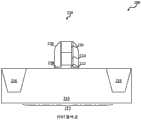
图1是根据本发明各个方面的用于制造集成电路器件的方法100的实施例的流程图。方法100开始于框110,在框110中,在衬底上方形成栅极结构。在框120中,通过例如蚀刻工艺去除部分衬底以形成第一凹槽和第二凹槽,以使栅极结构介于第一凹槽和第二凹槽之间。在框130中,在衬底中形成氮钝化层,以使第一凹槽和第二凹槽被衬底的氮钝化表面限定。在一个实例中,通过去耦等离子体氮化工艺形成氮钝化层。在框140中,在第一凹槽和第二凹槽的氮钝化表面上方形成掺杂的源极和漏极部件,并且所述掺杂的源极和漏极部件填充第一凹槽和第二凹槽。氮钝化的表面可以防止掺杂的源极和漏极部件中的掺杂剂向外扩散至衬底中。方法100可以继续完成集成电路器件的制造。在方法100之前、期间和之后可以提供额外的步骤,并且对于所述方法的其他实施例,所述步骤中的一些步骤可以被替换或者取消。下面的讨论示出了可根据图1的方法100制造的集成电路器件的各个实施例。FIG. 1 is a flowchart of an embodiment of a method 100 for fabricating an integrated circuit device in accordance with various aspects of the present invention. Method 100 begins at
图2至图5是根据图1的方法100在各个制造阶段期间的集成电路器件200的实施例的各个图解式剖面图。出于清楚的目的简化了图2至图5以便更好地理解本发明的发明概念。在所述的实施例中,如下面进一步所讨论的,集成电路器件200包括晶体管器件,具体来说是p-沟道金属氧化物半导体场效应晶体管(PFET)。可选地,集成电路器件200可以是n-沟道金属氧化物半导体场效应晶体管(NFET),在该情况中,在此描述的掺杂结构和材料应结合NFET一起理解(例如,与为NFET器件提供合适沟道的具有相反导电性的掺杂结构和材料一起理解)。集成电路器件200可以进一步包括存储器单元和/或逻辑电路;无源元件如电阻器、电容器、电感器、和/或熔丝;有源元件,如金属氧化物半导体场效应晶体管(MOSFET)、互补金属氧化物半导体晶体管(CMOS)、高电压晶体管、和/或高频率晶体管;其他合适的元件;或者其组合。在集成电路器件200中可以增加其他部件,并且对于集成电路器件200的其他实施例,下面所述的一些部件可以被替换或者去除。2-5 are various diagrammatic cross-sectional views of an embodiment of an
在图2中,提供了衬底210。在所述的实施例中,衬底210是包括硅的半导体衬底。衬底可以是p型或n型衬底。可选地或者另外地,衬底210包括另一元素半导体,如锗;化合物半导体,包括碳化硅、砷化镓、磷化镓、磷化铟、砷化铟、和/或锑化铟;合金半导体,包括SiGe、GaAsP、AlInAs、AlGaAs、GaInAs、GaInP、和/或GaInAsP;或者其组合。在又一个可选实施例中,衬底210是绝缘体上的半导体(SOI)。在其他可选实施例中,衬底210可以包括掺杂的外延层、梯度半导体层、和/或覆在另一不同类型的半导体层上面的半导体层,例如硅锗层上的硅层。In Figure 2, a
衬底210可以包括各种掺杂区,这取决于集成电路器件200(例如p型阱或n型阱)的设计要求。掺杂区可以使用以下掺杂剂掺杂:p型掺杂剂,如硼或BF2;n型掺杂剂,如磷或砷;或其组合。掺杂区可以以P-阱结构、N-阱结构、双阱结构直接形成在衬底210上,或者使用突起的结构直接形成在衬底210上。集成电路器件200包括配置为用于具体器件的器件区212。在所述实施例中,器件区212被配置为用于PFET器件。因此,器件区212可以包括配置为用于PFET器件的掺杂区。器件区212可以被称为PFET器件区。The
在衬底210中形成隔离部件216以隔离衬底210的各个区。例如,隔离部件216将器件区212与其他器件区(如配置成用于NFET器件的器件区)隔离开以及与其他器件(未示出)隔离开。隔离部件216采用隔离技术如硅的局部氧化(LOCOS)和/或浅沟槽隔离(STI)来限定并电隔离各个区。隔离部件216包括氧化硅、氮化硅、氮氧化硅、其他合适的材料、或其组合。通过任何合适的工艺形成隔离部件216。作为一个实例,形成STI包括光刻工艺;在衬底中蚀刻沟槽(例如,通过采用干法蚀刻、湿法蚀刻、或者其组合);以及用一种或多种介电材料填充沟槽(例如,通过采用化学汽相沉积工艺)。例如,经填充的沟槽可以具有多层结构,如填充有氮化硅或氧化硅的热氧化物衬层。在另一实例中,可以采用以下工艺顺序制造STI结构,如:生长焊盘氧化物(pad oxide),在焊盘氧化物上方形成低压化学汽相沉积(LPCVD)氮化物层,使用光刻胶和掩膜在焊盘氧化物和氮化物层中图案化STI开口,在STI开口中的衬底中蚀刻沟槽,可选地生长热氧化物沟槽衬层来改进沟槽界面,用氧化物填充沟槽,采用化学机械抛光(CMP)加工以回蚀刻及平坦化,以及采用氮化物剥离工艺去除氮化物层。Isolation features 216 are formed in the
在PFET器件区212中的衬底210上方设置栅极结构220。在所述的实施例中,栅极结构220包括栅极介电层222、栅极层224(被称为栅电极)、和硬掩膜层226。栅极介电层222、栅极层224、和硬掩膜层226形成栅叠层的栅极结构220。根据PFET器件的设计要求,栅叠层220可以包括其他层。通过沉积工艺、光刻图案化工艺、蚀刻工艺、或其组合形成栅极结构220(例如,栅叠层的各层)。沉积工艺包括化学汽相沉积(CVD)、物理汽相沉积(PVD)、原子层沉积(ALD)、高密度等离子体CVD(HDPCVD)、金属有机CVD(MOCVD)、远程等离子体CVD(RPCVD)、等离子体增强CVD(PECVD)、电镀、其他合适的沉积方法、或其组合。光刻图案化工艺包括光刻胶涂布(如旋转涂布)、软烘焙、掩膜对准、暴露、暴露后烘焙、光刻胶显影、冲洗、干燥(如硬烘焙)、其他合适的工艺、或其组合。可选地,实施光刻暴露工艺或者通过其他适当方法如无掩膜的光刻法、电子束书写、或离子束书写替换光刻暴露工艺。蚀刻工艺包括干法蚀刻、湿法蚀刻、其他蚀刻方法、或其组合。Gate structure 220 is disposed over
在衬底210上方形成栅极介电层222,栅极介电层222包括介电材料如氧化硅、氮氧化硅、氮化硅,高k介电材料,其他合适的介电材料;或其组合。示例性高k介电材料包括HfO2、HfSiO、HfSiON、HfTaO、HfTiO、HfZrO、Ta2O5、TiO2、Al2O3、ZrO2、Y2O3、L2O3、其他合适的材料、或者其组合。栅极介电层222可以包括多层结构。例如,栅极介电层222可以包括界面层以及在界面层上形成的高k介电材料层。示例性界面层可以是通过热处理工艺或ALD工艺形成的生长的氧化硅层。Forming a
在栅极介电层222上方形成栅极层224。在所述实施例中,栅极层224是多晶体硅(多晶硅)层。为达到适当的导电性可以掺杂多晶硅层。可选地,如果要形成伪栅极并在随后的栅极替换工艺中替换该伪栅极,则可以不必掺杂多晶硅。可选地,栅极层224包括具有适当功函数的导电层,因此,栅极层224也可以被称为功函数层。功函数层包括任何合适的材料,以使该层可以被调整成具有适当的功函数以实现增强关联器件的性能。例如,如果期望用于PFET器件的p型功函数金属(p-金属),如在所述实施例中,则导电层可以包括TiN或TaN。另一方面,如果期望用于NFET器件的n型功函数金属(n-金属),则导电层可以包括Ta、TiAl、TiAlN或TaCN。功函数层可以包括掺杂的导电氧化物材料。栅极层224可以包括其他导电材料如铝、铜、钨、金属合金、金属硅化物、其他合适的材料、或其组合。例如,当栅极层224包括功函数层时,可以在功函数层上方形成另一导电层。A
在栅极层224上方形成硬掩膜层226。硬掩膜层226包括氧化硅、氮化硅、氮氧化硅、碳化硅、其他合适的介电材料、或其组合。硬掩膜层226可以具有多层结构。A hard mask layer 226 is formed over the
对于栅极结构220可以形成间隔件衬层228和间隔件230。在所述实施例中,间隔件衬层228包括氧化物材料如氧化硅,以及间隔件230包括氮化物材料如氮化硅。可选地,间隔件230包括另一合适的介电材料如氧化硅、氮氧化硅、或其组合。间隔件衬层228也可以包括另一合适的介电材料。通过合适的工艺形成间隔件衬层228和间隔件230。例如,间隔件衬层228和间隔件230通过以下方式形成:通过在集成电路器件200上方均厚(blanket)沉积第一介电层(氧化硅层)以及在第一介电层上方均厚沉积第二介电层(氮化硅层),然后各向异性地蚀刻以去除介电层从而形成图2中所示出的间隔件衬层228和间隔件230。间隔件衬层228和间隔件230被设置为邻近栅极结构220的栅叠层(栅极介电层222、栅极层224、和硬掩膜层226)的侧壁。在所述实施例中,间隔件230是偏移(也被称为伪)间隔件,其将在后续的加工期间被去除。可选地,间隔件230可以是主间隔件(main spacer)并形成PFET器件的栅极结构的一部分。A
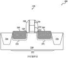
在图3中,在PFET器件区212中的PFET器件的源极区和漏极区中形成凹槽240。在所述实施例中,栅极结构220介于PFET器件的源极区和漏极区之间,并且在源极区和漏极区之间限定沟道区。凹槽240延伸进入衬底210一深度。在一种实例中,凹槽240延伸进入衬底210约60nm至约65nm的深度。在所述实施例中,蚀刻工艺去除部分衬底210以在衬底210上形成凹槽240。蚀刻工艺包括干法蚀刻工艺、湿法蚀刻工艺、或其组合。干法和湿法蚀刻工艺具有能够调整达到凹槽240的期望轮廓的蚀刻参数,如所用的蚀刻剂、蚀刻温度、蚀刻溶液浓度、蚀刻压力、电源功率、RF偏置电压、RF偏置功率、蚀刻剂流速、和其他合适的参数。在实例中,干法蚀刻工艺是等离子体蚀刻工艺,该等离子体蚀刻工艺使用含氟蚀刻剂、含氯蚀刻剂、含溴蚀刻剂、或者其他合适的蚀刻剂。在实例中,湿法蚀刻工艺使用湿法蚀刻溶液,该湿法蚀刻溶液包括:NH4OH、HF(氢氟酸)、TMAH(四甲基氢氧化铵)、其他合适的湿法蚀刻溶液、或其组合。在蚀刻工艺之后,可以实施预清洗工艺,以用HF溶液或其他合适的溶液清洗凹槽240。In FIG. 3 , recesses 240 are formed in the source and drain regions of the PFET devices in
在图4中,实施去耦等离子体氮化工艺250以沿着限定凹槽240的衬底210的表面形成钝化层252。去耦等离子体氮化工艺250使用电感耦合以生成含氮等离子体并将氮引入衬底210中,尤其是沿着限定凹槽240的衬底210的表面,以形成钝化层252。因此,凹槽240被衬底210的氮钝化表面限定。可以调整去耦等离子体氮化工艺250的各种参数如含氮气体、气体流速、温度、时间、电源功率、偏置电压、脉冲射频、和其他合适的参数以达到钝化层252的期望氮剂量和期望氮掺杂剂分布。在一种实例中,去耦等离子体氮化工艺250在约室温(例如,约20℃至约25℃)下将衬底210暴露于流速为约280sccm至约320sccm的含氮气体如N2,持续约90秒至约100秒。在实例中,衬底210暴露于含氮气体约30秒。在实例中,含氮气体的流速为约300sccm。In FIG. 4 , a decoupled
如下面进一步所述的,钝化层252(以及因此限定凹槽240的衬底210的氮钝化表面)提供沿着凹槽240的阻挡层,该阻挡层阻止可在后续掺杂工艺期间使用的掺杂剂如硼掺杂剂向外扩散。钝化层252从限定凹槽240的衬底210的表面向衬底210中延伸一深度。在所述实施例中,该深度小于或者等于约
去耦等离子体氮化工艺250替代通常用于沿着限定凹槽240的衬底210的表面形成碳注入物的碳注入工艺。尽管通过碳注入工艺形成的碳注入物有效地阻止了掺杂剂的向外扩散,但是需要退火工艺来激活碳注入物。这种退火不期望地增加了规定的用于制造集成电路器件200的热预算。通过用如本文所述的去耦等离子体氮化工艺250替代碳注入工艺,在无需实施额外的退火工艺的情况下获得了用于阻止后续加工期间掺杂剂向外扩散的阻挡物。也因此消除了采用碳注入工艺引起的热预算问题。通过实施去耦等离子体氮化工艺250,还降低了制造时间,因为可以去除退火步骤。The decoupled
在图5中,半导体材料被形成在凹槽240中以在PMOS器件区212形成应变结构。半导体材料形成在凹槽240中的源极和漏极部件260。源极和漏极部件260可以可选地被称为凸起的源极和漏极区。在所述实施例中,实施外延(epitaxy or epitaxial(epi))工艺以在凹槽240中沉积半导体材料。外延工艺可以包括选择性外延生长(SEG)工艺、CVD沉积技术(例如,汽相外延(VPE)和/或超高真空CVD(UHV-CVD))、分子束外延、其他合适的外延工艺、或者其组合。外延工艺可以使用气体和/或液体前体,其可以与衬底210的组分相互反应。沉积的半导体材料向PFET器件的沟道区提供压力或应力,以增强器件的载流子迁移率和增强器件性能。在所述的实施例中,通过外延工艺在衬底210的凹槽240中沉积硅锗(SiGe)以形成SiGe源极和漏极部件260。而且,在所述实施例中,源极和漏极部件260掺杂有合适的掺杂剂。例如,SiGe源极和漏极部件掺杂有硼(B)以形成SiGe:B源极和漏极部件。源极和漏极部件260可以掺杂有其他合适的掺杂剂,如碳(C)或锑(Sb)。可选地,源极和漏极部件260是掺杂有锑的硅(Si)源极和漏极部件(Si:Sb源极和漏极部件)。在又一个可选实施例中,源极和漏极部件260是掺杂有碳(C)的硅(Si)源极和漏极部件(Si:C源极和漏极部件)。可以是在外延工艺期间现场掺杂源极和漏极部件260,或者现场不掺杂然后在后续工艺中掺杂源极和漏极部件260。可以通过离子注入工艺、等离子体浸没离子注入(PIII)工艺、气体和/或固体源扩散工艺、其他合适的工艺、或其组合实现掺杂。源极和漏极部件260可以进一步暴露于退火工艺,如快速热退火工艺。In FIG. 5 , semiconductor material is formed in
如上面所注意到的,在源极和漏极部件260和衬底210之间设置的钝化层252提供了沿着凹槽240的阻挡层,所述阻挡层阻止掺杂剂如硼掺杂剂的向外扩散。因此,在源极和漏极部件260的掺杂期间,钝化层252阻止掺杂剂如硼向外扩散至衬底210中,尤其是阻止向外扩散至集成电路器件200的沟道区内(注意:沟道区被限定在PFET器件区212中的源极和漏极区之间,尤其是在栅极结构220下方以及在源极和漏极部件260之间)。钝化层252包括优化用于阻止掺杂剂向外扩散的氮与硅的比率,同时提供用于形成外延生长源极和漏极部件260的合适的衬底表面。优化氮与硅的比率可以依据用于形成源极和漏极部件260的工艺控制得如何。As noted above, the
集成电路器件200可以继续加工以完成制造,如下面所简要讨论的。例如,对于栅极结构220可以形成间隔件。在实例中,在形成源极和漏极部件260之后去除间隔件230(其在所述实施例中充当偏移或伪间隔件),并且随后可以形成用于栅极结构220的间隔件。可以通过n型掺杂剂如磷或砷或者p型掺杂剂如硼的离子注入形成轻掺杂的源极/漏极(LDD)区和/或重掺杂的源极/漏极(HDD)区。LDD和/或HDD区可以比所述实施例中更早地形成。另外,例如在凸起的源极/漏极部件上形成硅化物部件,以减少接触阻力。可以通过包括沉积金属层、退火金属层使得金属层能够与硅反应形成硅化物、然后去除未反应的金属层的工艺在源极和漏极部件上形成硅化物部件。
在衬底上形成层间介电(ILD)层,并且进一步对衬底应用化学机械抛光(CMP)工艺来平坦化衬底。可以在形成ILD层之前在栅极结构220的顶部上形成接触蚀刻停止层(CESL)。在一种实例中,成品器件的栅极层224保留多晶硅。在另一种实例中,多晶硅被去除,在后栅极或栅极替换工艺中用金属替换。在后栅极工艺中,对ILD层实施的CMP工艺继续暴露出栅极结构的硬掩膜层,并且实施蚀刻工艺来去除硬掩膜层和多晶硅,从而形成沟槽。然后用适当的功函数金属(例如p型功函数金属或n型功函数金属)填充沟槽。进一步地,包括金属层和金属层间电介质(IMD)的多层互连(MLI)形成在衬底210上方以电连接集成电路器件200的各种部件或结构。多层互连包括纵向互连件如常规通孔或接触件,以及横向互连件如金属线。各种互连部件可以应用各种导电材料,包括铜、钨和硅化物。在一个实例中,使用镶嵌工艺来形成铜多层互连结构。An interlayer dielectric (ILD) layer is formed on the substrate, and a chemical mechanical polishing (CMP) process is further applied to the substrate to planarize the substrate. A contact etch stop layer (CESL) may be formed on top of the gate structure 220 before forming the ILD layer. In one example, the
集成电路器件200作为一个实例。集成电路器件200可以用于各种应用如数字电路、成像传感器器件、异质半导体器件、动态随机存取存储器(DRAM)单元、单电子晶体管(SET)和/或其他微电子器件(在本文中合起来被称为微电子器件)。而且,本发明的各方面也适用于和/或很容易适应于其他类型晶体管,包括单栅极晶体管、双栅极晶体管和其它多栅极晶体管,并可以使用在许多不同的应用中,包括传感器单元、存储器单元、逻辑单元和其它的单元。
本发明提供实现了许多不同的实施例。不同的实施例可以具有不同的优点,但是没有特定的优点是任何实施例所必需的。在一种实例中,一种方法包括:提供衬底;在衬底上方形成栅极结构;去除部分衬底以在衬底中形成第一凹槽和第二凹槽,以使栅极结构介于第一凹槽和第二凹槽之间;在衬底中形成氮钝化层,以使第一凹槽和第二凹槽被所述衬底的氮钝化表面限定;以及在第一凹槽和第二凹槽的氮钝化表面的上方形成掺杂的源极和漏极部件,该掺杂的源极和漏极部件填充第一凹槽和第二凹槽。形成氮钝化层的步骤可以包括实施去耦等离子体氮化工艺,这可以包括将氮注入到衬底至小于或等于约
在实例中,衬底是硅衬底,并且形成氮钝化层的步骤包括优化氮钝化层的硅与氮的比率,以使在形成掺杂的源极和漏极部件时氮钝化层阻止掺杂剂向外扩散。在氮钝化表面上方形成掺杂的源极和漏极部件的步骤可以包括在氮钝化表面的上方外延生长半导体材料以及掺杂半导体材料。外延生长半导体材料可以是硅锗,并且该硅锗可以掺杂有硼。可以在外延生长半导体材料的同时或者外延生长半导体材料之后实施掺杂半导体材料。In an example, the substrate is a silicon substrate, and the step of forming the nitrogen passivation layer includes optimizing the ratio of silicon to nitrogen of the nitrogen passivation layer such that the nitrogen passivation layer Dopants are prevented from diffusing out. The step of forming doped source and drain features over the nitrogen passivated surface may include epitaxially growing a semiconductor material over the nitrogen passivated surface and doping the semiconductor material. The epitaxially grown semiconductor material may be silicon germanium, and the silicon germanium may be doped with boron. Doping the semiconductor material may be performed simultaneously with the epitaxial growth of the semiconductor material or after the epitaxial growth of the semiconductor material.
在另一实例中,一种方法包括:在衬底上方形成栅极结构;在衬底中形成邻近栅极结构的凹槽,其中该凹槽被衬底的表面限定;实施去耦等离子体氮化工艺,从而沿着限定凹槽的衬底的表面形成钝化层;以及在形成钝化层之后,在凹槽中形成掺杂的、外延半导体部件。去耦等离子体氮化工艺包括使用含氮气体,包括N2。可以在室温下如约20℃至约25℃的温度下实施去耦等离子体氮化工艺。掺杂的外延半导体部件可以包括掺杂有硼的外延硅锗部件。形成钝化层的步骤可以包括优化钝化层的氮浓度,以使在形成掺杂有硼的外延硅锗部件期间钝化层阻止硼扩散至衬底中。In another example, a method includes: forming a gate structure over a substrate; forming a recess in the substrate adjacent the gate structure, wherein the recess is defined by a surface of the substrate; applying a decoupling plasma nitrogen a passivation process to form a passivation layer along the surface of the substrate defining the recess; and after forming the passivation layer, form a doped, epitaxial semiconductor feature in the recess. The decoupled plasma nitridation process involves the use of nitrogen-containing gases, includingN2 . The decoupled plasma nitridation process may be performed at room temperature, eg, at a temperature of about 20°C to about 25°C. The doped epitaxial semiconductor component may comprise a boron-doped epitaxial silicon germanium component. The step of forming the passivation layer may include optimizing the nitrogen concentration of the passivation layer such that the passivation layer prevents boron from diffusing into the substrate during formation of the boron-doped epitaxial silicon germanium feature.
在又一个实例中,一种方法包括:在衬底上方形成栅极结构;在衬底中蚀刻源极凹槽和漏极凹槽,以使栅极结构介于源极凹槽和漏极凹槽之间;在不实施退火工艺的情况下,沿着限定源极凹槽和漏极凹槽的衬底的表面形成氮阻挡层;以及在源极凹槽和漏极凹槽中形成掺杂的源极和漏极部件,该掺杂的源极和漏极部件被设置在氮阻挡层上。在不实施退火工艺的情况下沿着限定源极凹槽和漏极凹槽的衬底的表面形成氮阻挡层可以包括实施去耦等离子体氮化工艺。在整个氮阻挡层中可以具有基本上一致的氮掺杂浓度。形成掺杂的源极和漏极部件的步骤可以包括:在源极凹槽和漏极凹槽中外延生长硅锗;以及用硼掺杂硅锗。在外延生长硅锗的同时或者在外延生长硅锗之后可以用硼掺杂硅锗。In yet another example, a method includes: forming a gate structure over a substrate; etching source and drain recesses in the substrate such that the gate structure is interposed between the source and drain recesses; between the grooves; without performing an annealing process, forming a nitrogen barrier layer along the surface of the substrate defining the source groove and the drain groove; and forming a doping layer in the source groove and the drain groove source and drain features, the doped source and drain features being disposed on the nitrogen barrier layer. Forming the nitrogen barrier layer along the surface of the substrate defining the source and drain grooves without performing an annealing process may include performing a decoupled plasma nitridation process. There may be a substantially uniform nitrogen doping concentration throughout the nitrogen barrier layer. The step of forming the doped source and drain features may include: epitaxially growing silicon germanium in the source groove and the drain groove; and doping the silicon germanium with boron. The silicon germanium may be doped with boron while the silicon germanium is epitaxially grown or after the silicon germanium is epitaxially grown.
在又一个实施例中,一种集成电路器件包括:衬底;以及设置在衬底上方的栅极结构,其中,该栅极结构介于衬底的源极区和漏极区之间。源极区和漏极区包括:设置衬底中的氮钝化层;以及设置在氮钝化层上的掺杂的外延半导体部件。在一个实例中,该掺杂的外延半导体部件包括掺杂有硼的硅锗。上面论述了若干实施例的部件,使得本领域技术人员可以更好地理解本发明的各个方面。本领域技术人员应该理解,可以很容易地使用本发明作为基础来设计或更改其他用于达到与本文所介绍实施例相同的目的和/或实现相同优点的工艺和结构。本领域技术人员也应该意识到,这种等效结构并不背离本发明的精神和范围,并且在不背离本发明的精神和范围的情况下,可以在其中进行多种变化、替换以及改变。In yet another embodiment, an integrated circuit device includes: a substrate; and a gate structure disposed over the substrate, wherein the gate structure is interposed between a source region and a drain region of the substrate. The source and drain regions include: a nitrogen passivation layer disposed in the substrate; and a doped epitaxial semiconductor component disposed on the nitrogen passivation layer. In one example, the doped epitaxial semiconductor component includes silicon germanium doped with boron. The components of several embodiments are discussed above so that those skilled in the art may better understand the various aspects of the invention. Those skilled in the art should understand that the present invention can be easily used as a basis to design or modify other processes and structures for achieving the same purpose and/or realizing the same advantages as the embodiments described herein. Those skilled in the art should also realize that such equivalent structures do not depart from the spirit and scope of the present invention, and that they can make various changes, substitutions and alterations herein without departing from the spirit and scope of the present invention.
Claims (10)

Applications Claiming Priority (2)
| Application Number | Priority Date | Filing Date | Title |
|---|---|---|---|
| US13/267,648 | 2011-10-06 | ||
| US13/267,648US8659089B2 (en) | 2011-10-06 | 2011-10-06 | Nitrogen passivation of source and drain recesses |
Publications (2)
| Publication Number | Publication Date |
|---|---|
| CN103035527Atrue CN103035527A (en) | 2013-04-10 |
| CN103035527B CN103035527B (en) | 2016-05-25 |
Family
ID=48022308
Family Applications (1)
| Application Number | Title | Priority Date | Filing Date |
|---|---|---|---|
| CN201210040862.8AExpired - Fee RelatedCN103035527B (en) | 2011-10-06 | 2012-02-21 | The nitrogen passivation of source electrode and drain recesses |
Country Status (2)
| Country | Link |
|---|---|
| US (1) | US8659089B2 (en) |
| CN (1) | CN103035527B (en) |
Cited By (4)
| Publication number | Priority date | Publication date | Assignee | Title |
|---|---|---|---|---|
| CN110246896A (en)* | 2018-03-07 | 2019-09-17 | 三星电子株式会社 | Semiconductor device and the method for manufacturing the semiconductor device |
| CN111244183A (en)* | 2014-01-24 | 2020-06-05 | 台湾积体电路制造股份有限公司 | Embedded source or drain regions of transistors with lateral extensions |
| WO2024098851A1 (en)* | 2022-11-08 | 2024-05-16 | 长鑫存储技术有限公司 | Semiconductor structure and forming method therefor |
| US12051752B2 (en) | 2014-01-24 | 2024-07-30 | Taiwan Semiconductor Manufacturing Company Ltd. | Embedded source or drain region of transistor with downward tapered region under facet region |
Families Citing this family (14)
| Publication number | Priority date | Publication date | Assignee | Title |
|---|---|---|---|---|
| US20140057399A1 (en)* | 2012-08-24 | 2014-02-27 | International Business Machines Corporation | Using Fast Anneal to Form Uniform Ni(Pt)Si(Ge) Contacts on SiGe Layer |
| US9029208B2 (en)* | 2012-11-30 | 2015-05-12 | International Business Machines Corporation | Semiconductor device with replacement metal gate and method for selective deposition of material for replacement metal gate |
| US9627480B2 (en) | 2014-06-26 | 2017-04-18 | Globalfoundries Inc. | Junction butting structure using nonuniform trench shape |
| US9627512B2 (en)* | 2014-08-13 | 2017-04-18 | Taiwan Semiconductor Manufacturing Company Ltd. | Field effect transistor with non-doped channel |
| US9634140B2 (en) | 2014-11-10 | 2017-04-25 | Samsung Electronics Co., Ltd. | Fabricating metal source-drain stressor in a MOS device channel |
| CN105762106B (en) | 2014-12-18 | 2021-02-19 | 联华电子股份有限公司 | Semiconductor device and manufacturing process thereof |
| US9887277B2 (en)* | 2015-01-23 | 2018-02-06 | Applied Materials, Inc. | Plasma treatment on metal-oxide TFT |
| KR102395071B1 (en) | 2015-05-14 | 2022-05-10 | 삼성전자주식회사 | Semiconductor devices including field effect transistors |
| US20180151733A1 (en)* | 2015-06-19 | 2018-05-31 | Intel Corporation | Carbon-based interface for epitaxially grown source/drain transistor regions |
| EP3311418A4 (en)* | 2015-06-19 | 2019-01-09 | Intel Corporation | REDUCTION OF RESISTANCE IN TRANSISTORS HAVING SOURCE / DRAIN REGIONS OBTAINED BY EPITAXIAL GROWTH |
| US9871100B2 (en) | 2015-07-29 | 2018-01-16 | Taiwan Semiconductor Manufacturing Co., Ltd. | Trench structure of semiconductor device having uneven nitrogen distribution liner |
| KR102502885B1 (en) | 2015-10-06 | 2023-02-23 | 삼성전자주식회사 | Semiconductor devices and methods of manufacturing the same |
| CN107403835B (en)* | 2016-05-19 | 2021-12-14 | 联芯集成电路制造(厦门)有限公司 | Semiconductor device and fabrication process thereof |
| KR102582670B1 (en)* | 2018-07-13 | 2023-09-25 | 삼성전자주식회사 | Semiconductor device |
Citations (3)
| Publication number | Priority date | Publication date | Assignee | Title |
|---|---|---|---|---|
| CN101022084A (en)* | 2006-02-14 | 2007-08-22 | 台湾积体电路制造股份有限公司 | Method of forming semiconductor device |
| CN101290886A (en)* | 2007-04-20 | 2008-10-22 | 中芯国际集成电路制造(上海)有限公司 | Manufacturing method of grid dielectric layer and grid |
| US20090026552A1 (en)* | 2007-07-27 | 2009-01-29 | Da Zhang | Method for forming a transistor having gate dielectric protection and structure |
Family Cites Families (5)
| Publication number | Priority date | Publication date | Assignee | Title |
|---|---|---|---|---|
| US20030157771A1 (en) | 2002-02-20 | 2003-08-21 | Tuung Luoh | Method of forming an ultra-thin gate dielectric by soft plasma nitridation |
| US7964514B2 (en)* | 2006-03-02 | 2011-06-21 | Applied Materials, Inc. | Multiple nitrogen plasma treatments for thin SiON dielectrics |
| US20080194091A1 (en) | 2007-02-13 | 2008-08-14 | Taiwan Semiconductor Manufacturing Co., Ltd. | Method for fabricating nitrided oxide layer |
| US7838887B2 (en) | 2008-04-30 | 2010-11-23 | Taiwan Semiconductor Manufacturing Company, Ltd. | Source/drain carbon implant and RTA anneal, pre-SiGe deposition |
| US20090321809A1 (en)* | 2008-06-30 | 2009-12-31 | Nirmal Ramaswamy | Graded oxy-nitride tunnel barrier |
- 2011
- 2011-10-06USUS13/267,648patent/US8659089B2/enactiveActive
- 2012
- 2012-02-21CNCN201210040862.8Apatent/CN103035527B/ennot_activeExpired - Fee Related
Patent Citations (3)
| Publication number | Priority date | Publication date | Assignee | Title |
|---|---|---|---|---|
| CN101022084A (en)* | 2006-02-14 | 2007-08-22 | 台湾积体电路制造股份有限公司 | Method of forming semiconductor device |
| CN101290886A (en)* | 2007-04-20 | 2008-10-22 | 中芯国际集成电路制造(上海)有限公司 | Manufacturing method of grid dielectric layer and grid |
| US20090026552A1 (en)* | 2007-07-27 | 2009-01-29 | Da Zhang | Method for forming a transistor having gate dielectric protection and structure |
Cited By (4)
| Publication number | Priority date | Publication date | Assignee | Title |
|---|---|---|---|---|
| CN111244183A (en)* | 2014-01-24 | 2020-06-05 | 台湾积体电路制造股份有限公司 | Embedded source or drain regions of transistors with lateral extensions |
| US12051752B2 (en) | 2014-01-24 | 2024-07-30 | Taiwan Semiconductor Manufacturing Company Ltd. | Embedded source or drain region of transistor with downward tapered region under facet region |
| CN110246896A (en)* | 2018-03-07 | 2019-09-17 | 三星电子株式会社 | Semiconductor device and the method for manufacturing the semiconductor device |
| WO2024098851A1 (en)* | 2022-11-08 | 2024-05-16 | 长鑫存储技术有限公司 | Semiconductor structure and forming method therefor |
Also Published As
| Publication number | Publication date |
|---|---|
| US8659089B2 (en) | 2014-02-25 |
| US20130087857A1 (en) | 2013-04-11 |
| CN103035527B (en) | 2016-05-25 |
Similar Documents
| Publication | Publication Date | Title |
|---|---|---|
| CN103035527B (en) | The nitrogen passivation of source electrode and drain recesses | |
| US12342610B2 (en) | Method of manufacturing semiconductor device | |
| US9349831B2 (en) | Integrated circuit device with well controlled surface proximity and method of manufacturing same | |
| CN102610637B (en) | Method of manufacturing strained source/drain structures | |
| US8216906B2 (en) | Method of manufacturing integrated circuit device with well controlled surface proximity | |
| CN102881576B (en) | Self-aligned source and drain electrode structure and manufacture method thereof | |
| CN102637728B (en) | Manufacture the method for strain source/drain structures | |
| US8569139B2 (en) | Method of manufacturing strained source/drain structures | |
| US9082789B2 (en) | Fabrication methods of integrated semiconductor structure | |
| US9246002B2 (en) | Structure and method for semiconductor device | |
| US10163724B2 (en) | Integrated circuit device and method of manufacturing same |
Legal Events
| Date | Code | Title | Description |
|---|---|---|---|
| C06 | Publication | ||
| PB01 | Publication | ||
| C10 | Entry into substantive examination | ||
| SE01 | Entry into force of request for substantive examination | ||
| C14 | Grant of patent or utility model | ||
| GR01 | Patent grant | ||
| CF01 | Termination of patent right due to non-payment of annual fee | ||
| CF01 | Termination of patent right due to non-payment of annual fee | Granted publication date:20160525 |