CN103034365A - Touch control display circuit structure and driving method, array substrate and display device thereof - Google Patents
Touch control display circuit structure and driving method, array substrate and display device thereofDownload PDFInfo
- Publication number
- CN103034365A CN103034365ACN2012105405749ACN201210540574ACN103034365ACN 103034365 ACN103034365 ACN 103034365ACN 2012105405749 ACN2012105405749 ACN 2012105405749ACN 201210540574 ACN201210540574 ACN 201210540574ACN 103034365 ACN103034365 ACN 103034365A
- Authority
- CN
- China
- Prior art keywords
- transistor
- touch
- electrode
- switching transistor
- line
- Prior art date
- Legal status (The legal status is an assumption and is not a legal conclusion. Google has not performed a legal analysis and makes no representation as to the accuracy of the status listed.)
- Granted
Links
Images


Classifications
- G—PHYSICS
- G06—COMPUTING OR CALCULATING; COUNTING
- G06F—ELECTRIC DIGITAL DATA PROCESSING
- G06F3/00—Input arrangements for transferring data to be processed into a form capable of being handled by the computer; Output arrangements for transferring data from processing unit to output unit, e.g. interface arrangements
- G06F3/01—Input arrangements or combined input and output arrangements for interaction between user and computer
- G06F3/03—Arrangements for converting the position or the displacement of a member into a coded form
- G06F3/041—Digitisers, e.g. for touch screens or touch pads, characterised by the transducing means
- G06F3/0416—Control or interface arrangements specially adapted for digitisers
- G—PHYSICS
- G06—COMPUTING OR CALCULATING; COUNTING
- G06F—ELECTRIC DIGITAL DATA PROCESSING
- G06F3/00—Input arrangements for transferring data to be processed into a form capable of being handled by the computer; Output arrangements for transferring data from processing unit to output unit, e.g. interface arrangements
- G06F3/01—Input arrangements or combined input and output arrangements for interaction between user and computer
- G06F3/03—Arrangements for converting the position or the displacement of a member into a coded form
- G06F3/041—Digitisers, e.g. for touch screens or touch pads, characterised by the transducing means
- G06F3/044—Digitisers, e.g. for touch screens or touch pads, characterised by the transducing means by capacitive means
- G06F3/0445—Digitisers, e.g. for touch screens or touch pads, characterised by the transducing means by capacitive means using two or more layers of sensing electrodes, e.g. using two layers of electrodes separated by a dielectric layer
- G—PHYSICS
- G06—COMPUTING OR CALCULATING; COUNTING
- G06F—ELECTRIC DIGITAL DATA PROCESSING
- G06F3/00—Input arrangements for transferring data to be processed into a form capable of being handled by the computer; Output arrangements for transferring data from processing unit to output unit, e.g. interface arrangements
- G06F3/01—Input arrangements or combined input and output arrangements for interaction between user and computer
- G06F3/03—Arrangements for converting the position or the displacement of a member into a coded form
- G06F3/041—Digitisers, e.g. for touch screens or touch pads, characterised by the transducing means
- G06F3/0412—Digitisers structurally integrated in a display
- G—PHYSICS
- G06—COMPUTING OR CALCULATING; COUNTING
- G06F—ELECTRIC DIGITAL DATA PROCESSING
- G06F3/00—Input arrangements for transferring data to be processed into a form capable of being handled by the computer; Output arrangements for transferring data from processing unit to output unit, e.g. interface arrangements
- G06F3/01—Input arrangements or combined input and output arrangements for interaction between user and computer
- G06F3/03—Arrangements for converting the position or the displacement of a member into a coded form
- G06F3/041—Digitisers, e.g. for touch screens or touch pads, characterised by the transducing means
- G06F3/044—Digitisers, e.g. for touch screens or touch pads, characterised by the transducing means by capacitive means
- G—PHYSICS
- G09—EDUCATION; CRYPTOGRAPHY; DISPLAY; ADVERTISING; SEALS
- G09G—ARRANGEMENTS OR CIRCUITS FOR CONTROL OF INDICATING DEVICES USING STATIC MEANS TO PRESENT VARIABLE INFORMATION
- G09G3/00—Control arrangements or circuits, of interest only in connection with visual indicators other than cathode-ray tubes
- G09G3/20—Control arrangements or circuits, of interest only in connection with visual indicators other than cathode-ray tubes for presentation of an assembly of a number of characters, e.g. a page, by composing the assembly by combination of individual elements arranged in a matrix no fixed position being assigned to or needed to be assigned to the individual characters or partial characters
- G09G3/34—Control arrangements or circuits, of interest only in connection with visual indicators other than cathode-ray tubes for presentation of an assembly of a number of characters, e.g. a page, by composing the assembly by combination of individual elements arranged in a matrix no fixed position being assigned to or needed to be assigned to the individual characters or partial characters by control of light from an independent source
- G09G3/36—Control arrangements or circuits, of interest only in connection with visual indicators other than cathode-ray tubes for presentation of an assembly of a number of characters, e.g. a page, by composing the assembly by combination of individual elements arranged in a matrix no fixed position being assigned to or needed to be assigned to the individual characters or partial characters by control of light from an independent source using liquid crystals
- G09G3/3611—Control of matrices with row and column drivers
- G09G3/3648—Control of matrices with row and column drivers using an active matrix
- G—PHYSICS
- G06—COMPUTING OR CALCULATING; COUNTING
- G06F—ELECTRIC DIGITAL DATA PROCESSING
- G06F2203/00—Indexing scheme relating to G06F3/00 - G06F3/048
- G06F2203/041—Indexing scheme relating to G06F3/041 - G06F3/045
- G06F2203/04103—Manufacturing, i.e. details related to manufacturing processes specially suited for touch sensitive devices
- G—PHYSICS
- G09—EDUCATION; CRYPTOGRAPHY; DISPLAY; ADVERTISING; SEALS
- G09G—ARRANGEMENTS OR CIRCUITS FOR CONTROL OF INDICATING DEVICES USING STATIC MEANS TO PRESENT VARIABLE INFORMATION
- G09G2300/00—Aspects of the constitution of display devices
- G09G2300/04—Structural and physical details of display devices
- G09G2300/0439—Pixel structures
- G09G2300/0465—Improved aperture ratio, e.g. by size reduction of the pixel circuit, e.g. for improving the pixel density or the maximum displayable luminance or brightness
- G—PHYSICS
- G09—EDUCATION; CRYPTOGRAPHY; DISPLAY; ADVERTISING; SEALS
- G09G—ARRANGEMENTS OR CIRCUITS FOR CONTROL OF INDICATING DEVICES USING STATIC MEANS TO PRESENT VARIABLE INFORMATION
- G09G2354/00—Aspects of interface with display user
Landscapes
- Engineering & Computer Science (AREA)
- Theoretical Computer Science (AREA)
- General Engineering & Computer Science (AREA)
- Physics & Mathematics (AREA)
- General Physics & Mathematics (AREA)
- Human Computer Interaction (AREA)
- Chemical & Material Sciences (AREA)
- Crystallography & Structural Chemistry (AREA)
- Computer Hardware Design (AREA)
- Liquid Crystal (AREA)
- Devices For Indicating Variable Information By Combining Individual Elements (AREA)
- Control Of Indicators Other Than Cathode Ray Tubes (AREA)
- Position Input By Displaying (AREA)
- Liquid Crystal Display Device Control (AREA)
Abstract
Translated fromChineseDescription
Translated fromChinese技术领域technical field
本发明涉及显示器制造领域,尤其涉及一种触控显示电路结构及其驱动方法、阵列基板和显示装置。The present invention relates to the field of display manufacturing, in particular to a touch display circuit structure and a driving method thereof, an array substrate and a display device.
背景技术Background technique
AD-SDS(Advanced-Super Dimensional Switching,简称为ADS,高级超维场开关)技术显示凭借其宽广的视角、更高的对比率、更高的分辨率及更明亮的颜色呈现,逐渐被消费者所追捧。在ADS模式下,通过同一层平面内狭缝电极边缘所产生的电场以及不同层的狭缝电极层与板状电极层间产生的电场形成多维电场,使液晶盒内狭缝电极间、电极正上方所有取向液晶分子都能够产生旋转,从而提高了液晶工作效率并增大了透光效率。对in cell touch(像素单元内部触控)技术关注将越来越大,目前大部分厂家对于触控技术的实现还是在显示显示装置的出光侧设置一层用于触控的电容薄膜、有少部分厂家在ADS显示模组上使用in cell touch技术,并已经成功量产,但是发明人发现在现有技术中,存在产品制程工艺繁琐,且制成品开口率较低的问题。AD-SDS (Advanced-Super Dimensional Switching, referred to as ADS, Advanced Super Dimensional Field Switch) technology display is gradually adopted by consumers due to its wide viewing angle, higher contrast ratio, higher resolution and brighter color presentation. sought after. In the ADS mode, the electric field generated by the edge of the slit electrode in the same plane and the electric field generated between the slit electrode layer and the plate electrode layer of different layers form a multi-dimensional electric field, so that the slit electrodes in the liquid crystal cell and the electrodes are positive All the aligned liquid crystal molecules above can be rotated, thereby improving the working efficiency of the liquid crystal and increasing the light transmission efficiency. More and more attention will be paid to in cell touch (internal touch control of pixel units). At present, most manufacturers still set a layer of capacitive film for touch control on the light-emitting side of the display device for the realization of touch technology. Some manufacturers have used in cell touch technology on ADS display modules and have successfully mass-produced them. However, the inventors found that in the prior art, the product manufacturing process is cumbersome and the aperture ratio of the finished product is low.
发明内容Contents of the invention
本发明的实施例提供一种触控显示电路结构及其驱动方法、阵列基板和显示装置,能够减少触摸显示产品生产过程中的制程工艺,节约成本,同时能够提高产品开口率增加附加值。Embodiments of the present invention provide a touch display circuit structure and its driving method, an array substrate, and a display device, which can reduce the manufacturing process in the production process of touch display products, save costs, and increase the product aperture ratio to increase added value.
为达到上述目的,本发明的实施例采用如下技术方案:In order to achieve the above object, embodiments of the present invention adopt the following technical solutions:
一方面,提供一种触控显示电路结构,包括触控单元和显示单元;与所述触控单元连接的第一扫描线、第二扫描线、检测信号线、数据线及信号控制线;与所述显示单元连接的栅线和数据线;On the one hand, a touch display circuit structure is provided, including a touch unit and a display unit; a first scan line, a second scan line, a detection signal line, a data line, and a signal control line connected to the touch unit; and Gate lines and data lines connected to the display unit;
其中所述触控单元包括第一开关晶体管、第二开关晶体管、第一电容、触控电极及放大晶体管;Wherein the touch unit includes a first switch transistor, a second switch transistor, a first capacitor, a touch electrode and an amplifying transistor;
所述第一开关晶体管的源极连接所述数据线,所述第一开关晶体管的栅极连接所述信号控制线;The source of the first switching transistor is connected to the data line, and the gate of the first switching transistor is connected to the signal control line;
所述触控电极连接所述第一开关晶体管的漏极;The touch electrode is connected to the drain of the first switch transistor;
所述放大晶体管的栅极连接所述触控电极,所述放大晶体管的源极连接所述第二扫描线;The gate of the amplifying transistor is connected to the touch electrode, and the source of the amplifying transistor is connected to the second scanning line;
所述第二开关晶体管的栅极连接所述第一扫描线,所述第二开关晶体管的源极连接所述放大晶体管的漏极,所述第二开关晶体管的漏极连接所述检测信号线;The gate of the second switching transistor is connected to the first scanning line, the source of the second switching transistor is connected to the drain of the amplification transistor, and the drain of the second switching transistor is connected to the detection signal line ;
所述第一电容的第一极连接所述第二扫描线,所述第一电容的第二极连接所述触控电极。A first pole of the first capacitor is connected to the second scan line, and a second pole of the first capacitor is connected to the touch electrode.
可选的,所述显示单元包括:Optionally, the display unit includes:
第三开关晶体管及第二电容;a third switch transistor and a second capacitor;
其中所述第三开关晶体管的栅极连接所述栅线,所述第三晶体管的源极连接所述数据线;Wherein the gate of the third switching transistor is connected to the gate line, and the source of the third transistor is connected to the data line;
所述第二电容的第一极连接所述第三开关晶体管的漏极,所述第二电容的第二极连接接地端。A first pole of the second capacitor is connected to the drain of the third switch transistor, and a second pole of the second capacitor is connected to a ground terminal.
可选的,所述第一电容的第一极为与所述显示单元的像素电极同层的透明导电材料;所述第一电容的第二极为与所述显示单元的公共电极同层的透明导电材料。Optionally, the first pole of the first capacitor is a transparent conductive material on the same layer as the pixel electrode of the display unit; the second pole of the first capacitor is a transparent conductive material on the same layer as the common electrode of the display unit. Material.
可选的,所述第三开关晶体管为“P”型晶体管或“N型晶体管”。Optionally, the third switch transistor is a "P" type transistor or an "N type transistor".
可选的,所述第一开关晶体管和所述第二开关晶体管为“P”型晶体管或“N型晶体管”;Optionally, the first switch transistor and the second switch transistor are "P" type transistors or "N type transistors";
所述放大晶体管为“P”型晶体管。The amplifying transistor is a "P" type transistor.
一方面,提供一种触控显示电路结构的驱动方法,包括:In one aspect, a method for driving a touch display circuit structure is provided, including:
第一阶段,第一开关晶体管、第二开关晶体管和放大晶体管截止,栅线输入扫描信号、本极数据线输入控制信号控制所述显示单元处于显示状态;In the first stage, the first switching transistor, the second switching transistor and the amplifying transistor are turned off, and the gate line inputs the scanning signal and the local data line inputs the control signal to control the display unit to be in the display state;
第二阶段,所述第一开关晶体管导通,所述第二开关晶体管和所述放大晶体管截止,所述数据线输入重置信号为第一电容的第二极充电,所述栅线输入扫描信号关闭所述显示单元;In the second phase, the first switching transistor is turned on, the second switching transistor and the amplifying transistor are turned off, the data line inputs a reset signal to charge the second electrode of the first capacitor, and the gate line inputs a scanning signal to turn off the display unit;
第三阶段,所述第一开关晶体管截止,所述第二开关晶体管导通,第二扫描线提供耦合脉冲信号,当触控电极受到触摸时,所述第一电容的第二极放电直至所述放大晶体管的栅极和源极的电压差等于所述放大晶体管的阈值电压,所述放大晶体管导通并处于放大状态将所述第二扫描线提供耦合脉冲信号放大输出至检测信号线。In the third stage, the first switch transistor is turned off, the second switch transistor is turned on, and the second scanning line provides a coupling pulse signal. When the touch electrode is touched, the second electrode of the first capacitor discharges until the The voltage difference between the gate and source of the amplifying transistor is equal to the threshold voltage of the amplifying transistor, and the amplifying transistor is turned on and in an amplified state to amplify and output the coupling pulse signal provided by the second scanning line to the detection signal line.
可选的,还包括:Optionally, also include:
所述第一阶段,所述第三开关晶体管导通;In the first stage, the third switch transistor is turned on;
所述第二阶段和所述第三阶段所述第三开关晶体管截止。The third switching transistor is turned off in the second phase and the third phase.
一方面,提供一种阵列基板,其特征在于,所述阵列基板的至少一个像素单元包括上述任一触控显示电路结构。In one aspect, an array substrate is provided, wherein at least one pixel unit of the array substrate includes any touch display circuit structure described above.
可选的,所述检测信号线为所述阵列基板上的一条数据线,包含所述触控显示电路结构的本级像素单元处于所述检测信号线与所述本级像素单元的数据线之间,所述检测信号线为所述本级像素单元的前一级像素单元提供显示驱动信号。Optionally, the detection signal line is a data line on the array substrate, and the current-level pixel unit including the touch display circuit structure is located between the detection signal line and the data line of the current-level pixel unit. During this period, the detection signal line provides a display driving signal for the pixel unit of the previous level of the pixel unit of the current level.
一方面,提供一种显示装置,包括上述的阵列基板。In one aspect, a display device is provided, including the above-mentioned array substrate.
本发明的实施例提供一种触控显示电路结构及其驱动方法、阵列基板和显示装置,将触控结构的电路和显示单元的电路集成在一起,能够通过显示单元的制程流程同时形成本发明实施例提供的触控结构,能够减少触摸显示产品生产过程中的制程工艺,节约成本,同时能够提高产品开口率增加附加值。Embodiments of the present invention provide a touch display circuit structure and its driving method, an array substrate, and a display device. The circuit of the touch structure and the circuit of the display unit are integrated, and the present invention can be simultaneously formed through the process flow of the display unit. The touch control structure provided by the embodiment can reduce the manufacturing process in the production process of the touch display product, save cost, and can increase the aperture ratio of the product and increase the added value.
附图说明Description of drawings
为了更清楚地说明本发明实施例或现有技术中的技术方案,下面将对实施例或现有技术描述中所需要使用的附图作简单地介绍,显而易见地,下面描述中的附图仅仅是本发明的一些实施例,对于本领域普通技术人员来讲,在不付出创造性劳动的前提下,还可以根据这些附图获得其他的附图。In order to more clearly illustrate the technical solutions in the embodiments of the present invention or the prior art, the following will briefly introduce the drawings that need to be used in the description of the embodiments or the prior art. Obviously, the accompanying drawings in the following description are only These are some embodiments of the present invention. Those skilled in the art can also obtain other drawings based on these drawings without creative work.
图1为本发明的实施例提供的一种触控显示电路结构示意图;FIG. 1 is a schematic structural diagram of a touch display circuit provided by an embodiment of the present invention;
图2为本发明的实施例提供的一种触控显示电路结构的驱动信号时序状态示意图;FIG. 2 is a schematic diagram of a driving signal timing state of a touch display circuit structure provided by an embodiment of the present invention;
图3为本发明的实施例提供的一种触控显示电路结构触控电极电压变化示意图;FIG. 3 is a schematic diagram of voltage changes of touch electrodes of a touch display circuit structure provided by an embodiment of the present invention;
图4为本发明的实施例提供的一种阵列基板显示电路结构示意图;FIG. 4 is a schematic structural diagram of an array substrate display circuit provided by an embodiment of the present invention;
图5为本发明的实施例提供的一种显示单元为ADS模式的阵列基板示意图。FIG. 5 is a schematic diagram of an array substrate with a display unit in ADS mode provided by an embodiment of the present invention.
具体实施方式Detailed ways
下面将结合本发明实施例中的附图,对本发明实施例中的技术方案进行清楚、完整地描述,显然,所描述的实施例仅仅是本发明一部分实施例,而不是全部的实施例。基于本发明中的实施例,本领域普通技术人员在没有做出创造性劳动前提下所获得的所有其他实施例,都属于本发明保护的范围。The following will clearly and completely describe the technical solutions in the embodiments of the present invention with reference to the accompanying drawings in the embodiments of the present invention. Obviously, the described embodiments are only some, not all, embodiments of the present invention. Based on the embodiments of the present invention, all other embodiments obtained by persons of ordinary skill in the art without making creative efforts belong to the protection scope of the present invention.
本发明所有实施例中采用的开关晶体管和放大晶体管均可以为薄膜晶体管或场效应管或其他特性相同的器件,由于这里采用的开关晶体管的源极、漏极是对称的,所以其源极、漏极是可以互换的。在本发明实施例中,为区分晶体管除栅极之外的两极,将其中一极称为源极,另一极称为漏极。按附图中的形态规定晶体管的中间端为栅极、信号输入端为源极、信号输出端为漏极。此外本发明实施例所采用的开关晶体管包括P型开关晶体管和N型开关晶体管两种,其中,P型开关晶体管在栅极为低电平时导通,在栅极为高电平时截止,N型开关晶体管为在栅极为高电平时导通,在栅极为低电平时截止;放大晶体管包括P型和N型,其中P型放大晶体管在栅极电压为低电平(栅极电压小于源极电压),且栅极源极的压差的绝对值大于阈值电压时处于放大状态,可以将源极的输入电压放大后在漏极输出;其中N型放大晶体管的栅极电压为高电平(栅极电压大于源极电压),且栅极源极的压差的绝对值大于阈值电压时处于放大状态,可以将源极的输入电压放大后在漏极输出,当然本发明的实施例只是采用了P型的放大晶体管。The switching transistors and amplifying transistors used in all embodiments of the present invention can be thin film transistors or field effect transistors or other devices with the same characteristics. Since the source and drain of the switching transistors used here are symmetrical, the source, Drains are interchangeable. In the embodiment of the present invention, in order to distinguish the two poles of the transistor except the gate, one pole is called the source, and the other pole is called the drain. According to the form in the accompanying drawings, it is stipulated that the middle terminal of the transistor is the gate, the signal input terminal is the source terminal, and the signal output terminal is the drain terminal. In addition, the switching transistors used in the embodiments of the present invention include P-type switching transistors and N-type switching transistors, wherein the P-type switching transistors are turned on when the gate is at a low level, and are turned off when the gate is at a high level, and the N-type switching transistors In order to turn on when the gate is at a high level, and to turn off when the gate is at a low level; the amplifying transistor includes P-type and N-type, wherein the P-type amplifying transistor is at a low level at the gate voltage (the gate voltage is less than the source voltage), And when the absolute value of the voltage difference between the gate and the source is greater than the threshold voltage, it is in an amplified state, and the input voltage of the source can be amplified and then output at the drain; wherein the gate voltage of the N-type amplifying transistor is high level (gate voltage greater than the source voltage), and the absolute value of the gate-source voltage difference is greater than the threshold voltage, it is in an amplified state, and the input voltage of the source can be amplified and then output at the drain. Of course, the embodiment of the present invention only uses a P-type amplifier transistor.
参照图1所示,为本发明的实施例提供的一种触控显示电路结构,包括触控单元1和显示单元2;与触控单元1连接的第一扫描线S1、第二扫描线S2、检测信号线Dn-1、数据线Dn及信号控制线K1;与显示单元2连接的栅线Gn和数据线Dn;Referring to FIG. 1 , a touch display circuit structure provided for an embodiment of the present invention includes a touch unit 1 and a display unit 2; a first scan line S1 and a second scan line S2 connected to the touch unit 1 , detection signal line Dn-1, data line Dn and signal control line K1; gate line Gn and data line Dn connected to the display unit 2;
其中触控单元1包括第一开关晶体管T1、第二开关晶体管T2、第一电容C1、触控电极N1及放大晶体管T3;The touch unit 1 includes a first switch transistor T1, a second switch transistor T2, a first capacitor C1, a touch electrode N1 and an amplifier transistor T3;
第一开关晶体管T1的源极连接数据线Dn,第一开关晶体管T1的栅极连接信号控制线K1;The source of the first switching transistor T1 is connected to the data line Dn, and the gate of the first switching transistor T1 is connected to the signal control line K1;
触控电极N1连接第一开关晶体管T1的漏极;The touch electrode N1 is connected to the drain of the first switching transistor T1;
放大晶体管T3的栅极连接触控电极N1,放大晶体管T3的源极连接第二扫描线S2;The gate of the amplifying transistor T3 is connected to the touch electrode N1, and the source of the amplifying transistor T3 is connected to the second scanning line S2;
第二开关晶体管T2的栅极连接第一扫描线S1,第二开关晶体管T2的源极连接放大晶体管T3的漏极,第二开关晶体管T2的漏极连接检测信号线Dn-1;The gate of the second switching transistor T2 is connected to the first scanning line S1, the source of the second switching transistor T2 is connected to the drain of the amplification transistor T3, and the drain of the second switching transistor T2 is connected to the detection signal line Dn-1;
第一电容C1的第一极连接第二扫描线S2,第一电容C1的第二极连接触控电极N1。A first pole of the first capacitor C1 is connected to the second scan line S2, and a second pole of the first capacitor C1 is connected to the touch electrode N1.
这里第一电容可以在制作显示单元的制程工艺中形成。Here, the first capacitor can be formed during the manufacturing process of the display unit.
优选的,结合制作ADS模式的显示单元2制作第一电容,其中第一电容的一极与制作显示单元的公共电极的同一次构图工艺形成,第一电容的另一极与制作显示单元的像素电极的同一次构图工艺形成,即第一电容的第一极为与显示单元的像素电极同层的透明导电材料;第一电容的第二极为与显示单元的公共电极同层的透明导电材料。即在制作显示单元2的公共电极和像素电极时,保留触控单元1的部分公共电极和部分像素电极,利用触控单元1的公共电极层与像素电极之间的交叠形成第一电容。当然,触控单元1和显示单元2这两个区域的公共电极之间和像素电极之间都是断开的。例如图5,显示单元2的公共电极59为狭缝电极,像素电极55为板状电极。Preferably, the first capacitor is made in combination with the display unit 2 of the ADS mode, wherein one pole of the first capacitor is formed with the same patterning process of making the common electrode of the display unit, and the other pole of the first capacitor is connected to the pixel of the display unit. The electrodes are formed by the same patterning process, that is, the first pole of the first capacitor is a transparent conductive material on the same layer as the pixel electrode of the display unit; the second pole of the first capacitor is a transparent conductive material on the same layer as the common electrode of the display unit. That is, when the common electrode and the pixel electrode of the display unit 2 are manufactured, part of the common electrode and part of the pixel electrode of the touch unit 1 are reserved, and the first capacitance is formed by overlapping between the common electrode layer of the touch unit 1 and the pixel electrode. Certainly, the common electrodes and the pixel electrodes in the two regions of the touch control unit 1 and the display unit 2 are all disconnected. For example, in FIG. 5 , the
当然,其中第一电容的一极可以与制作显示单元的像素电极的同一次构图工艺形成,第一电容的另一极与制作显示单元的公共电极的同一次构图工艺形成。Of course, one pole of the first capacitor can be formed in the same patterning process as the pixel electrode of the display unit, and the other pole of the first capacitor can be formed in the same patterning process as the common electrode of the display unit.
进一步的,触控电极N1与制作显示单元2的像素电极在同一次构图工艺形成,即由显示单元的像素电极同层的透明导电材料构成;且第一电容C1的第二极与触控电极N1通过过孔连接。当然过孔的深度由制作显示单元的公共电极与像素电极之间的距离而定。Further, the touch electrode N1 and the pixel electrode of the display unit 2 are formed in the same patterning process, that is, the pixel electrode of the display unit is formed of the same layer of transparent conductive material; and the second electrode of the first capacitor C1 is connected to the touch electrode N1 is connected through vias. Of course, the depth of the via hole is determined by the distance between the common electrode and the pixel electrode for making the display unit.
进一步的,触控单元1的所有晶体管与显示单元2的晶体管同步形成。Further, all the transistors of the touch control unit 1 are formed synchronously with the transistors of the display unit 2 .
进一步的,第二开关晶体管T2和放大晶体管T3位于触控电极N1的一侧,第一开关晶体管T1位于触控电极N1相对的另一侧。Further, the second switching transistor T2 and the amplifying transistor T3 are located on one side of the touch electrode N1, and the first switching transistor T1 is located on the opposite side of the touch electrode N1.
进一步的,第一扫描线S1、第二扫描线S2、及信号控制线K1均与显示单元2的栅线同步形成;且与栅线平行设置,均位于显示单元2的间隙之间,不影响显示单元2的开口率。其中,如图5所示,显示单元2的栅线可以与显示单元2的栅极52在同一次构图工艺中形成。Further, the first scanning line S1, the second scanning line S2, and the signal control line K1 are all formed synchronously with the grid lines of the display unit 2; Displays the aperture ratio of unit 2. Wherein, as shown in FIG. 5 , the gate line of the display unit 2 and the
进一步的,为了布线需要和信号的输入,同一触控显示电路结构的第一扫描线S1、第二扫描线S2位于靠近第二开关晶体管T2和放大晶体管T3的一侧,即位于栅线Gn的外侧,栅线Gn内侧连接显示单元2的第三开关晶体管T4;信号控制线K1位于靠近第一开关晶体管T1的一侧,即位于栅线Gn+1(未示出)的外侧,栅线Gn+1内侧连接Gn+1行的显示单元。Further, for wiring requirements and signal input, the first scanning line S1 and the second scanning line S2 of the same touch display circuit structure are located on the side close to the second switching transistor T2 and the amplifying transistor T3, that is, on the side of the gate line Gn. Outside, the inside of the gate line Gn is connected to the third switching transistor T4 of the display unit 2; the signal control line K1 is located on the side close to the first switching transistor T1, that is, outside the gate line Gn+1 (not shown), the gate line Gn The +1 inner side is connected to the display unit of the Gn+1 row.
进一步的,第一开关晶体管T1,第二开关晶体管T2以及放大晶体管T3均可以通过制作显示单元2时在触控单元1中保留的数据线层(例如数据线Dn)作为连接线,与其他部件进行连接,并在需要的地方进行过孔连接。例如:第二开关晶体管T2的栅极通过制作显示单元2在触控单元1中保留的数据线层(例如数据线Dn)作为连接线,连接第一扫描线S1,并在需要的地方进行过孔连接。比如,在该连接线靠近第一扫描线S1的一端进行过孔连接。过孔的深度和位置,取决于第一扫描线S1与数据线层的层间距离以及部件之间的位置关系。其中,如图5所示,显示单元2中的数据线层可以与源极56,漏极57在同一次构图工艺中形成。Further, the first switching transistor T1, the second switching transistor T2 and the amplifying transistor T3 can be connected with other components by using the data line layer (such as the data line Dn) reserved in the touch unit 1 when the display unit 2 is manufactured as a connection line. Make connections and make via connections where needed. For example: the gate of the second switching transistor T2 is connected to the first scanning line S1 by making the data line layer (such as the data line Dn) reserved in the touch unit 1 of the display unit 2 as a connection line, and is processed where necessary. hole connection. For example, a via connection is performed at an end of the connecting line close to the first scanning line S1. The depth and position of the via hole depend on the interlayer distance between the first scan line S1 and the data line layer and the positional relationship between components. Wherein, as shown in FIG. 5 , the data line layer in the display unit 2 can be formed in the same patterning process as the source electrode 56 and the
所述构图工艺可以包括制作图形的掩膜、曝光、显影、光刻,刻蚀等过程。The patterning process may include making a graphic mask, exposure, development, photolithography, etching and other processes.
举例来说,采用构图工艺在基板上形成栅极,具体为:首先在基板上沉积栅极层薄膜,然后涂布光刻胶,利用掩膜板对光刻胶进行曝光和显影处理来形成光刻胶图案,接着利用该光刻胶图案作为蚀刻掩模,通过刻蚀等工艺去除相应的电极层,并且去除剩余的光刻胶,最终在基板上形成栅极图形。For example, a patterning process is used to form a gate on a substrate, specifically: first deposit a gate layer film on the substrate, then coat a photoresist, and use a mask to expose and develop the photoresist to form a photo Resist pattern, and then use the photoresist pattern as an etching mask to remove the corresponding electrode layer through etching and other processes, and remove the remaining photoresist, and finally form the gate pattern on the substrate.
可选的,显示单元2包括:Optionally, the display unit 2 includes:
第三开关晶体管T4及第二电容C2;其中第二电容C2包括显示单元2的像素电极与公共电极之间的液晶电容及第三开关晶体管T4的寄生电容;The third switching transistor T4 and the second capacitor C2; wherein the second capacitor C2 includes the liquid crystal capacitance between the pixel electrode and the common electrode of the display unit 2 and the parasitic capacitance of the third switching transistor T4;
其中第三开关晶体管T4的栅极连接栅线Gn,第三晶体管T4的源极连接数据线Dn;The gate of the third switching transistor T4 is connected to the gate line Gn, and the source of the third transistor T4 is connected to the data line Dn;
像素电极作为第二电容C2的第一极连接第三开关晶体管T4的漏极,公共电极作为第二电容T2的第二极连接接地端VSS。The pixel electrode serves as the first pole of the second capacitor C2 and is connected to the drain of the third switching transistor T4, and the common electrode serves as the second pole of the second capacitor T2 and is connected to the ground terminal VSS.
可选的,第一开关晶体管T1和第二开关晶体管T2为“P”型晶体管或“N型晶体管”;放大晶体管T3为“P”型晶体管。Optionally, the first switch transistor T1 and the second switch transistor T2 are "P" type transistors or "N type transistors"; the amplifying transistor T3 is a "P" type transistor.
可选的,第三开关晶体管T4为“P”型晶体管或“N型晶体管”。Optionally, the third switch transistor T4 is a "P" type transistor or an "N type transistor".
本发明的实施例提供的触控显示电路结构,将触控结构的电路和显示单元的电路集成在一起,能够通过显示单元的制程流程同时形成本发明实施例提供的触控结构,能够减少触摸显示产品生产过程中的制程工艺,节约成本,同时能够提高产品开口率增加附加值。The touch display circuit structure provided by the embodiment of the present invention integrates the circuit of the touch structure and the circuit of the display unit, and can simultaneously form the touch structure provided by the embodiment of the present invention through the process flow of the display unit, which can reduce touch Display the process technology in the production process of the product, save costs, and at the same time increase the product opening rate and increase the added value.
参照以上各实施例提供的触控显示电路本发明实施例还提供了以上各实施例触控显示电路的驱动方法:Referring to the touch display circuit provided in the above embodiments, the embodiment of the present invention also provides a driving method for the touch display circuit in the above embodiments:
第一阶段,第一开关晶体管T1、第二开关晶体管T2和放大晶体管T3截止,栅线Gn输入扫描信号、数据线Dn输入控制信号控制显示单元2处于显示状态;In the first stage, the first switching transistor T1, the second switching transistor T2 and the amplifying transistor T3 are turned off, the gate line Gn inputs a scan signal, and the data line Dn inputs a control signal to control the display unit 2 to be in a display state;
第二阶段,第一开关晶体管T1导通,第二开关晶体管T2和放大晶体管T3截止,数据线Dn输入重置信号为第一电容C1的第二极充电,栅线Gn输入扫描信号关闭显示单元2;In the second stage, the first switching transistor T1 is turned on, the second switching transistor T2 and the amplifying transistor T3 are turned off, the data line Dn inputs a reset signal to charge the second electrode of the first capacitor C1, and the gate line Gn inputs a scanning signal to turn off the display unit 2;
第三阶段,第一开关晶体管T1截止,第二开关晶体管T2导通,第二扫描线S2提供耦合脉冲信号,当触控电极N1受到触摸时,第一电容C1的第二极放电直至放大晶体管T3的栅极和源极的电压差等于放大晶体管T3的阈值电压,放大晶体管T3导通并处于放大状态将第二扫描线S2提供的耦合脉冲信号放大输出至检测信号线Dn-1。In the third stage, the first switching transistor T1 is turned off, the second switching transistor T2 is turned on, and the second scanning line S2 provides a coupling pulse signal. When the touch electrode N1 is touched, the second electrode of the first capacitor C1 discharges until the amplifying transistor The voltage difference between the gate and the source of T3 is equal to the threshold voltage of the amplifying transistor T3, and the amplifying transistor T3 is turned on and in an amplifying state to amplify and output the coupling pulse signal provided by the second scanning line S2 to the detection signal line Dn-1.
进一步的,第一阶段,第三开关晶体管T4导通;第二阶段和第三阶段第三开关晶体管T4截止。Further, in the first stage, the third switching transistor T4 is turned on; in the second and third stages, the third switching transistor T4 is turned off.
这里对第一开关晶体管T1、所述第二开关晶体管T2、放大晶体管T3和第三开关晶体管T4均采用“P”型晶体管为例进行说明。参照图1提供的电路图及图2提供的触控显示电路的信号时序状态示意图,对本发明实施例提供一种触控显示电路的驱动方法进行详细说明,具体包括:Here, the first switching transistor T1 , the second switching transistor T2 , the amplifying transistor T3 and the third switching transistor T4 all use "P" type transistors as an example for illustration. Referring to the circuit diagram provided in FIG. 1 and the signal timing state schematic diagram of the touch display circuit provided in FIG. 2 , a driving method for a touch display circuit provided by an embodiment of the present invention will be described in detail, specifically including:
第一阶段,即图2中所示的时序状态示意图中的第一时间段,栅线Gn、第二扫描线S2施加低电平信号,信号控制线K1及第一扫描线S1施加高电平,数据线Dn施加输出灰阶信号,此时显示单元的第三开关晶体管T4导通,由于数据线Dn施加输出灰阶信号,此时显示单元处于显示阶段;第一开关晶体管T1、第二开关晶体管T2及放大晶体管均处于截止状态,因此触控单元不工作。The first stage, that is, the first time period in the timing state schematic diagram shown in Figure 2, the gate line Gn, the second scan line S2 apply a low level signal, and the signal control line K1 and the first scan line S1 apply a high level , the data line Dn applies the output gray-scale signal, and at this time the third switch transistor T4 of the display unit is turned on, because the data line Dn applies the output gray-scale signal, and the display unit is in the display stage at this time; the first switch transistor T1, the second switch Both the transistor T2 and the amplifier transistor are in cut-off state, so the touch unit does not work.
第二阶段,即图2中所示的时序状态示意图中的第二时间段,栅线Gn、第一扫描线S2施加高电平信号,信号控制线K1及第二扫描线S1施加低电平,数据线Dn施加高电平重置信号,此时显示单元的第三开关晶体管T4截止,显示结束;触控单元的第一开关晶体管T1导通,此时数据线Dn上施加的高电平重置信号为与触控电极N1连接的第一电容C1充电,此时触控电极N1连接的A节点的电压升高至V1,该过程为下一阶段做准备。The second stage, that is, the second time period in the timing state schematic diagram shown in Figure 2, the gate line Gn, the first scan line S2 apply a high level signal, and the signal control line K1 and the second scan line S1 apply a low level , the data line Dn applies a high-level reset signal, at this time the third switching transistor T4 of the display unit is turned off, and the display ends; the first switching transistor T1 of the touch unit is turned on, and at this time the high level applied to the data line Dn The reset signal charges the first capacitor C1 connected to the touch electrode N1, at this time, the voltage of the node A connected to the touch electrode N1 rises to V1, and this process prepares for the next stage.
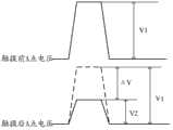
第三阶段,即图2所示的时序状态示意图中的第三时间段,栅线Gn、信号控制线K1、第二扫描线S2均施加高电平信号,第一扫描线施加低电平信号,此时显示单元的第三开关晶体管T4截止,触控单元的第一开关晶体管截止;第二开关晶体管T2导通;此阶段第二扫描线S2为第一电容的一极提供高电平,形成耦合电容,参照图3所示,由于在第二阶段为第一电容充电在触控电极上形成电压V1,当手指对触控电极N1上方触摸时,则会导致触控电极上的电压下降,此时信号控制线K1为第一电容提供的耦合电压同样会保持放大晶体管T3的源极电压,由于放大晶体管T3的栅极连接触控电极,则当触控电极上的电压下降至V2,产生的电压降ΔV满足放大晶体管的导通条件时(这里导通条件即栅极电压和源极电压差的绝对值大于晶体管的导通阈值电压,由于采用P型晶体管因此晶体管导通时栅极电压小于源极电压),放大晶体管T3导通并处于放大状态,由于第二开关晶体管T2导通,则放大晶体管T3会将第二扫描线S2上的高电平信号放大后输出至检测信号线Dn-1,此时通过第一扫描线S1确定第一坐标方向,通过检测信号线Dn-1上输出的信号变化值确定与第一坐标方向垂直的第二坐标方向,便可定位到触摸位置。The third stage, that is, the third time period in the timing state schematic diagram shown in Figure 2, the gate line Gn, the signal control line K1, and the second scanning line S2 all apply a high-level signal, and the first scanning line applies a low-level signal At this time, the third switching transistor T4 of the display unit is turned off, the first switching transistor of the touch unit is turned off; the second switching transistor T2 is turned on; at this stage, the second scanning line S2 provides a high level for one pole of the first capacitor, Form a coupling capacitor, as shown in Figure 3, because the first capacitor is charged in the second stage to form a voltage V1 on the touch electrode, when the finger touches the top of the touch electrode N1, the voltage on the touch electrode will drop At this time, the coupling voltage provided by the signal control line K1 for the first capacitor will also maintain the source voltage of the amplifying transistor T3. Since the gate of the amplifying transistor T3 is connected to the touch electrode, when the voltage on the touch electrode drops to V2, When the generated voltage drop ΔV meets the conduction condition of the amplifying transistor (the conduction condition here is that the absolute value of the difference between the gate voltage and the source voltage is greater than the conduction threshold voltage of the transistor, since the P-type transistor is used, the gate of the transistor is turned on voltage is less than the source voltage), the amplifying transistor T3 is turned on and in the amplified state, and since the second switching transistor T2 is turned on, the amplifying transistor T3 will amplify the high-level signal on the second scanning line S2 and output it to the detection signal line Dn-1, at this time, the first coordinate direction is determined by the first scanning line S1, the second coordinate direction perpendicular to the first coordinate direction is determined by detecting the signal change value output on the signal line Dn-1, and the touch position can be located .
这里以第一扫描线S1的信号为X轴坐标方向的信号,以检测信号线Dn-1的信号为Y轴坐标方向坐标方向,当第一扫描线S1输入信号时,便确定了X轴方向的坐标,此时由于第二开关晶体管T2导通,则放大晶体管T3会将第二扫描线S2上的高电平信号放大后输出至检测信号线Dn-1,此时当检测到检测信号线Dn-1上的信号变化情况时,边同时确定了X、Y两个坐标轴上的坐标位置,据此便确定了触摸位置。Here, the signal of the first scanning line S1 is used as the signal of the X-axis coordinate direction, and the signal of the detection signal line Dn-1 is used as the coordinate direction of the Y-axis coordinate direction. When the signal is input from the first scanning line S1, the X-axis direction is determined. At this time, since the second switching transistor T2 is turned on, the amplifying transistor T3 will amplify the high-level signal on the second scanning line S2 and output it to the detection signal line Dn-1. At this time, when the detection signal line When the signal on Dn-1 changes, the coordinate positions on the X and Y coordinate axes are determined simultaneously, and the touch position is determined accordingly.
这里在第三阶段结束之后,本级之后的其他栅线陆续输入控制信号,实现其他像素的驱动,由于阵列基板上每条数据线上的信号设计是相同的,因此,对于本发明的实施例所提供的触控显示电路是分时驱动的,即在触控阶段数据线输入的是用作触控的信号,而在显示阶段输入用作像素驱动灰阶信号,此外根据上述的驱动时序状态图,可知数据线在第二阶段和第三阶段是不用作显示灰阶信号输入的,因此触控信号在用作信号检测线Dn-1的上一级数据线上输出不会影响到显示装置的正常灰阶输出,而当放大晶体管T3将第二扫描线S2上的高电平信号放大后输出至检测信号线Dn-1时,便可通过检测信号线Dn-1检测到此时的信号与原先输入的触控信号的变化值。Here, after the end of the third stage, other gate lines after this stage input control signals one after another to realize the driving of other pixels. Since the signal design of each data line on the array substrate is the same, therefore, for the embodiment of the present invention The provided touch display circuit is driven by time division, that is, the input of the data line is used as a touch signal in the touch phase, and the input is used as a pixel driving grayscale signal in the display phase. In addition, according to the above-mentioned driving timing state As shown in the figure, it can be seen that the data line is not used for display grayscale signal input in the second stage and the third stage, so the output of the touch signal on the upper data line used as the signal detection line Dn-1 will not affect the display device normal grayscale output, and when the amplifying transistor T3 amplifies the high-level signal on the second scanning line S2 and outputs it to the detection signal line Dn-1, the signal at this time can be detected through the detection signal line Dn-1 The change value from the original input touch signal.
本发明的实施例对具体的晶体管的类型不做限制,当然在采用全P型时,更加有利于制程过程中减少工艺流程,同时由于所有晶体管可以同时形成更加有利于器件性能的统一,这里就体现出了采用LTPS工艺的优势,使用这种工艺形成的晶体管器件,除了载流子迁移速率高以外(可以将晶体管做小,提高开口率),另外,能够使得放大晶体管T3具有较高的击穿电压,同时,放大晶体管T3的栅极信号会随手指的触控而降低,因此使用P型晶体管更容易实现放大晶体管T3栅源之间的压差的绝对值(栅极电压Vg<源极电压Vs)大于Vth。The embodiment of the present invention does not limit the type of specific transistors. Of course, when the all-P type is used, it is more conducive to reducing the process flow in the manufacturing process. At the same time, since all transistors can be formed at the same time, it is more conducive to the unity of device performance. Here is It reflects the advantages of adopting LTPS technology. The transistor device formed by using this technology not only has a high carrier mobility rate (the transistor can be made smaller and the aperture ratio can be increased), but also can make the amplifying transistor T3 have a higher impact. At the same time, the gate signal of the amplifying transistor T3 will decrease with the touch of the finger, so it is easier to use a P-type transistor to realize the absolute value of the voltage difference between the gate and source of the amplifying transistor T3 (gate voltage Vg<source The voltage Vs) is greater than Vth.
本发明的实施例提供一种阵列基板,该阵列基板的至少一个像素单元包括上述实施例提供的任一触控显示电路结构。可选的,检测信号线为阵列基板上的一条数据线,包含触控显示电路结构的本级像素单元处于检测信号线与本级像素单元的数据线之间,检测信号线为本级像素单元的前一级像素单元提供显示驱动信号。An embodiment of the present invention provides an array substrate, at least one pixel unit of the array substrate includes any touch display circuit structure provided in the above embodiments. Optionally, the detection signal line is a data line on the array substrate, the current-level pixel unit including the touch display circuit structure is located between the detection signal line and the data line of the current-level pixel unit, and the detection signal line is the current-level pixel unit The previous level of pixel units provide display driving signals.
其中包含本发明实施例提供的触控显示电路结构的像素单元在阵列基板上的分布密度根据该阵列基板能够提供的像素大小、对触控精度的要求可以任意设置,当对触控精度要求高时相应的增加设置的密度,当然这样会对影响到面板的整体透过率,如图4所示,本发明的实施例提供了一种触控显示电路在阵列基板上4×4分布的显示单元电路结构示意图,即在阵列基板上按横向或纵向每四个像素单元中有一个包含有本发明的实施例所提供的触控显示电路结构。此外如图4所示,包含本发明的实施例提供的触控显示电路结构的像素单元中的检测信号线(前一级像素单元的数据线)Dn-1,检测信号线作Dn-1为阵列基板上的一条数据线与包含触控显示电路结构的本级像素单元的数据线相邻,本级像素单元处于检测信号线与本级像素单元的数据线之间,该检测信号线连接前一级像素单元的显示单元为其提供显示驱动信号。The distribution density of the pixel units including the touch display circuit structure provided by the embodiment of the present invention on the array substrate can be set arbitrarily according to the pixel size that the array substrate can provide and the requirements for touch accuracy. When increasing the setting density correspondingly, of course, this will affect the overall transmittance of the panel. As shown in FIG. A schematic diagram of a unit circuit structure, that is, one of every four pixel units in the horizontal or vertical direction on the array substrate includes the touch display circuit structure provided by the embodiment of the present invention. In addition, as shown in FIG. 4 , the detection signal line (data line of the previous pixel unit) Dn-1 in the pixel unit including the touch display circuit structure provided by the embodiment of the present invention, the detection signal line Dn-1 is A data line on the array substrate is adjacent to the data line of the pixel unit of the current level including the touch display circuit structure. The pixel unit of the current level is between the detection signal line and the data line of the pixel unit of the current level. Before the detection signal line is connected The display unit of the first-level pixel unit provides display driving signals therefor.
其中图4还给出了触控显示电路所在的当前像素单元在阵列基板上与对应的信号线的连接结构,参照图4所示,以包含本发明的实施例提供的触控显示电路的像素单元41为例,该触控显示电路结构分别连接栅线Gn、第一扫描线S1、第二扫描线S2、信号控制线K1、数据线Dn及检测信号线Dn-1(上一级像素单元的数据线);此外图中还给出了下一级像素单元的数据线Dn+1、上一级栅线Gn-1(即在时序上先于本级的栅线Gn给出开关信号的栅线)、下一级栅线Gn+1(即在时序上紧邻本级的栅线Gn下一个给出开关信号的栅线)。Figure 4 also shows the connection structure of the current pixel unit where the touch display circuit is located on the array substrate and the corresponding signal line, as shown in Figure 4, to include the pixel of the touch display circuit provided by the embodiment of the present invention Taking unit 41 as an example, the touch display circuit structure is respectively connected to the gate line Gn, the first scanning line S1, the second scanning line S2, the signal control line K1, the data line Dn and the detection signal line Dn-1 (upper level pixel unit In addition, the data line Dn+1 of the pixel unit of the next level and the gate line Gn-1 of the upper level are also shown in the figure (that is, the gate line Gn of the current level gives the switching signal in timing gate line), and the gate line Gn+1 of the next stage (that is, the next gate line next to the gate line Gn of the current stage in terms of timing) that provides the switching signal).
如图5所示,本发明的实施例提供的一种显示单元为ADS模式的阵列基板。其中,在衬底基板51上形成有栅极522,在栅极52上形成有栅极绝缘层53,栅极绝缘层53上形成有有源层54,有源层54上形成有像素电极55和源极56、漏极57,其中像素电极55与漏极57连接,在像素电极55和源极56、漏极57上形成有保护层58,在保护层58上形成有公共电极59,其中公共电极59为狭缝状电极,像素电极55为板状电极。当然本发明不局限于该种结构的ADS模式,在此不作限定。例如还可以是公共电极59为板状电极,像素电极55为狭缝状电极。该结构的具体制作工艺和工作原理为现有技术,在此不再赘述。As shown in FIG. 5 , a display unit provided by an embodiment of the present invention is an array substrate in an ADS mode. Wherein, a gate 522 is formed on the
本发明的实施例提供的阵列基板,将触控结构的电路和显示单元的电路集成在一起,能够通过显示单元的制程流程同时形成本发明实施例提供的触控结构,能够减少触摸显示产品生产过程中的制程工艺,节约成本,同时能够提高产品开口率增加附加值。The array substrate provided by the embodiment of the present invention integrates the circuit of the touch structure and the circuit of the display unit, and can simultaneously form the touch structure provided by the embodiment of the present invention through the process flow of the display unit, which can reduce the production of touch display products. The process technology in the process saves costs, and at the same time can increase the product opening rate and increase added value.
本发明的实施例提供一种显示装置,该显示装置包括上述实施例提供的阵列基板。另外,显示装置还可以为电子纸、手机、电视、数码相框等等显示设备。Embodiments of the present invention provide a display device, which includes the array substrate provided in the above embodiments. In addition, the display device may also be a display device such as an electronic paper, a mobile phone, a television, a digital photo frame, and the like.
本发明实施例提供的显示装置,将触控结构的电路和显示单元的电路集成在一起,能够通过显示单元的制程流程同时形成本发明实施例提供的触控结构,能够减少触摸显示产品生产过程中的制程工艺,节约成本,同时能够提高产品开口率增加附加值。The display device provided by the embodiment of the present invention integrates the circuit of the touch structure and the circuit of the display unit, and can simultaneously form the touch structure provided by the embodiment of the present invention through the process flow of the display unit, which can reduce the production process of touch display products. The advanced process technology saves cost, and at the same time, it can increase the product aperture ratio and increase the added value.
以上所述,仅为本发明的具体实施方式,但本发明的保护范围并不局限于此,任何熟悉本技术领域的技术人员在本发明揭露的技术范围内,可轻易想到变化或替换,都应涵盖在本发明的保护范围之内。因此,本发明的保护范围应以所述权利要求的保护范围为准。The above is only a specific embodiment of the present invention, but the scope of protection of the present invention is not limited thereto. Anyone skilled in the art can easily think of changes or substitutions within the technical scope disclosed in the present invention. Should be covered within the protection scope of the present invention. Therefore, the protection scope of the present invention should be determined by the protection scope of the claims.
Claims (10)
Priority Applications (5)
| Application Number | Priority Date | Filing Date | Title |
|---|---|---|---|
| CN201210540574.9ACN103034365B (en) | 2012-12-13 | 2012-12-13 | Touch display circuit structure and driving method, array base palte and display device |
| EP13195481.0AEP2743913A1 (en) | 2012-12-13 | 2013-12-03 | Touch display circuit, drive method thereof, array substrate and display device |
| KR1020130153986AKR101537868B1 (en) | 2012-12-13 | 2013-12-11 | Touch display circuit, drive method thereof, array substrate and display device |
| JP2013256785AJP6276015B2 (en) | 2012-12-13 | 2013-12-12 | Touch display circuit, driving method thereof, array substrate, and display device |
| US14/106,618US9671906B2 (en) | 2012-12-13 | 2013-12-13 | Touch display circuit, drive method thereof, array substrate and display device |
Applications Claiming Priority (1)
| Application Number | Priority Date | Filing Date | Title |
|---|---|---|---|
| CN201210540574.9ACN103034365B (en) | 2012-12-13 | 2012-12-13 | Touch display circuit structure and driving method, array base palte and display device |
Publications (2)
| Publication Number | Publication Date |
|---|---|
| CN103034365Atrue CN103034365A (en) | 2013-04-10 |
| CN103034365B CN103034365B (en) | 2016-03-09 |
Family
ID=48021315
Family Applications (1)
| Application Number | Title | Priority Date | Filing Date |
|---|---|---|---|
| CN201210540574.9AExpired - Fee RelatedCN103034365B (en) | 2012-12-13 | 2012-12-13 | Touch display circuit structure and driving method, array base palte and display device |
Country Status (5)
| Country | Link |
|---|---|
| US (1) | US9671906B2 (en) |
| EP (1) | EP2743913A1 (en) |
| JP (1) | JP6276015B2 (en) |
| KR (1) | KR101537868B1 (en) |
| CN (1) | CN103034365B (en) |
Cited By (17)
| Publication number | Priority date | Publication date | Assignee | Title |
|---|---|---|---|---|
| CN103235457A (en)* | 2013-04-25 | 2013-08-07 | 北京京东方光电科技有限公司 | Touch pixel driving circuit, method, array substrate and liquid crystal display device |
| CN103246396A (en)* | 2013-04-18 | 2013-08-14 | 北京京东方光电科技有限公司 | Touch display circuit structure and driving method thereof, array substrate and display device |
| CN103761002A (en)* | 2013-12-31 | 2014-04-30 | 北京大学深圳研究生院 | Touch circuit, touch circuit unit, touch display panel and touch display device |
| CN104064140A (en)* | 2014-06-09 | 2014-09-24 | 京东方科技集团股份有限公司 | Pixel circuit, drive method of pixel circuit, organic light-emitting display panel and display device |
| CN104103239A (en)* | 2014-06-23 | 2014-10-15 | 京东方科技集团股份有限公司 | Organic light-emitting diode pixel circuit and driving method thereof |
| WO2014173021A1 (en)* | 2013-04-26 | 2014-10-30 | 北京京东方光电科技有限公司 | Pixel unit control circuit and display device |
| CN104834423A (en)* | 2015-05-11 | 2015-08-12 | 叶志 | Touch panel array |
| CN106356014A (en)* | 2015-07-14 | 2017-01-25 | 冠捷投资有限公司 | Circuit structure of embedded touch display panel |
| US9639193B2 (en) | 2013-04-25 | 2017-05-02 | Beijing Boe Optoelectronics Technology Co., Ltd. | Touch-control pixel driving circuit, touch-control pixel driving method, array substrate and liquid crystal display (LCD) device |
| CN107943353A (en)* | 2016-10-13 | 2018-04-20 | 敦泰电子股份有限公司 | Electronic device and driving method thereof |
| US9984272B2 (en) | 2014-09-26 | 2018-05-29 | Boe Technology Group Co., Ltd. | Pixel circuit, its driving method, light-emitting diode display panel, and display device |
| CN111339962A (en)* | 2020-02-28 | 2020-06-26 | 重庆京东方光电科技有限公司 | Identification substrate, display panel, manufacturing method of display panel and display device |
| CN112799538A (en)* | 2021-01-19 | 2021-05-14 | 京东方科技集团股份有限公司 | A touch driving method, a touch driving device and a touch display device |
| CN113138477A (en)* | 2021-04-23 | 2021-07-20 | 深圳市华星光电半导体显示技术有限公司 | Display panel and electronic device |
| CN114023187A (en)* | 2021-10-26 | 2022-02-08 | 深圳市爱协生科技有限公司 | Touch-controlled segment code display screen |
| CN114721553A (en)* | 2022-06-06 | 2022-07-08 | 惠科股份有限公司 | Touch structure, OLED touch display panel and manufacturing method |
| US11676552B2 (en) | 2021-04-23 | 2023-06-13 | Shenzhen China Star Optoelectronics Semiconductor Display Technology Co., Ltd. | Display panel and electronic device |
Families Citing this family (17)
| Publication number | Priority date | Publication date | Assignee | Title |
|---|---|---|---|---|
| KR102417266B1 (en) | 2015-01-27 | 2022-07-05 | 삼성디스플레이 주식회사 | Display device and touch sensing method thereof |
| CN104778923B (en)* | 2015-04-28 | 2016-06-01 | 京东方科技集团股份有限公司 | A kind of image element circuit and driving method, display unit |
| CN104866158B (en)* | 2015-06-18 | 2017-12-15 | 京东方科技集团股份有限公司 | A kind of In-cell touch panel and display device |
| CN105301822B (en)* | 2015-12-11 | 2018-10-23 | 上海中航光电子有限公司 | A kind of array substrate, display panel and display device |
| CN105373259B (en)* | 2015-12-11 | 2018-11-27 | 上海中航光电子有限公司 | A kind of array substrate, display panel and display device |
| CN105527768A (en)* | 2016-01-25 | 2016-04-27 | 武汉华星光电技术有限公司 | Liquid crystal display device and liquid crystal display panel thereof |
| CN105808014B (en) | 2016-05-19 | 2019-07-02 | 京东方科技集团股份有限公司 | An array substrate, a method for making the same, and a touch display device |
| CN105867032A (en)* | 2016-06-01 | 2016-08-17 | 深圳市华星光电技术有限公司 | Liquid crystal display, display module and TFT array substrate thereof |
| CN106648212B (en)* | 2016-10-31 | 2020-04-03 | 京东方科技集团股份有限公司 | A display substrate, device and manufacturing method |
| CN108663837B (en)* | 2017-03-31 | 2021-01-22 | 京东方科技集团股份有限公司 | Touch display unit, touch display substrate, touch display panel and driving method thereof |
| CN107562279B (en)* | 2017-09-14 | 2020-07-10 | 敦泰电子有限公司 | Embedded self-capacitance touch liquid crystal display device and data processing chip and screen body thereof |
| KR102502201B1 (en)* | 2017-11-17 | 2023-02-22 | 삼성디스플레이 주식회사 | Fingerprint sensor and display device including the same |
| CN108646483B (en)* | 2018-04-26 | 2021-08-24 | 上海中航光电子有限公司 | Array substrate, display panel and display device |
| CN109324720B (en)* | 2018-09-28 | 2023-09-26 | 武汉华星光电技术有限公司 | Array substrate, touch display screen and driving method of array substrate |
| CN110264961B (en)* | 2019-04-04 | 2022-08-02 | 上海中航光电子有限公司 | Driving circuit and driving method thereof, panel and driving method thereof |
| US11749192B2 (en)* | 2020-03-19 | 2023-09-05 | Boe Technology Group Co., Ltd. | Display substrate and display device |
| KR20240033372A (en)* | 2022-09-05 | 2024-03-12 | 엘지디스플레이 주식회사 | Display device |
Citations (3)
| Publication number | Priority date | Publication date | Assignee | Title |
|---|---|---|---|---|
| CN101581845A (en)* | 2008-05-16 | 2009-11-18 | 精工爱普生株式会社 | Electro-optical device, electronic apparatus, and contact detection method |
| US20110193816A1 (en)* | 2008-11-14 | 2011-08-11 | Sharp Kabushiki Kaisha | Capacitance change detecting circuit |
| US20120044176A1 (en)* | 2010-08-19 | 2012-02-23 | Toshiba Mobile Display Co., Ltd. | Display device |
Family Cites Families (11)
| Publication number | Priority date | Publication date | Assignee | Title |
|---|---|---|---|---|
| TWI363206B (en)* | 2003-02-28 | 2012-05-01 | Samsung Electronics Co Ltd | Liquid crystal display device |
| JP4834482B2 (en)* | 2006-07-24 | 2011-12-14 | 東芝モバイルディスプレイ株式会社 | Display device |
| JP4894768B2 (en)* | 2008-01-28 | 2012-03-14 | ソニー株式会社 | Display device and electronic device |
| US8451233B2 (en)* | 2008-02-13 | 2013-05-28 | Himax Technologies Limited | Sensor pixel and touch panel thereof |
| JP5217618B2 (en)* | 2008-05-16 | 2013-06-19 | セイコーエプソン株式会社 | Method for identifying contact position of electronic equipment |
| JP2011237489A (en)* | 2010-05-06 | 2011-11-24 | Toshiba Mobile Display Co Ltd | Organic el display device |
| KR20120014808A (en)* | 2010-08-10 | 2012-02-20 | 엘지디스플레이 주식회사 | LCD including touch sensor, driving method thereof and manufacturing method thereof |
| CN102156565B (en)* | 2010-12-31 | 2014-11-05 | 深圳超多维光电子有限公司 | Display equipment and method, and naked eye three-dimensional display device |
| JP5581261B2 (en)* | 2011-04-27 | 2014-08-27 | 株式会社ジャパンディスプレイ | Semiconductor device, display device and electronic apparatus |
| KR101776064B1 (en)* | 2011-06-10 | 2017-09-08 | 삼성디스플레이 주식회사 | Touch Screen Panel |
| KR101890799B1 (en)* | 2012-02-07 | 2018-08-23 | 삼성디스플레이 주식회사 | Thin-film transistor array substrate, organic light emitting display device comprising the same and manufacturing method of the same |
- 2012
- 2012-12-13CNCN201210540574.9Apatent/CN103034365B/ennot_activeExpired - Fee Related
- 2013
- 2013-12-03EPEP13195481.0Apatent/EP2743913A1/ennot_activeCeased
- 2013-12-11KRKR1020130153986Apatent/KR101537868B1/ennot_activeExpired - Fee Related
- 2013-12-12JPJP2013256785Apatent/JP6276015B2/ennot_activeExpired - Fee Related
- 2013-12-13USUS14/106,618patent/US9671906B2/ennot_activeExpired - Fee Related
Patent Citations (3)
| Publication number | Priority date | Publication date | Assignee | Title |
|---|---|---|---|---|
| CN101581845A (en)* | 2008-05-16 | 2009-11-18 | 精工爱普生株式会社 | Electro-optical device, electronic apparatus, and contact detection method |
| US20110193816A1 (en)* | 2008-11-14 | 2011-08-11 | Sharp Kabushiki Kaisha | Capacitance change detecting circuit |
| US20120044176A1 (en)* | 2010-08-19 | 2012-02-23 | Toshiba Mobile Display Co., Ltd. | Display device |
Cited By (36)
| Publication number | Priority date | Publication date | Assignee | Title |
|---|---|---|---|---|
| WO2014169535A1 (en)* | 2013-04-18 | 2014-10-23 | 北京京东方光电科技有限公司 | Touch display circuit structure and driving method thereof, array substrate and display device |
| CN103246396A (en)* | 2013-04-18 | 2013-08-14 | 北京京东方光电科技有限公司 | Touch display circuit structure and driving method thereof, array substrate and display device |
| US9529467B2 (en) | 2013-04-18 | 2016-12-27 | Boe Technology Group Co., Ltd. | Touch display circuit, driving method thereof, array substrate and display apparatus |
| JP2016522429A (en)* | 2013-04-18 | 2016-07-28 | 北京京東方光電科技有限公司 | Touch control display circuit configuration and driving method thereof, array substrate, and display device |
| CN103246396B (en)* | 2013-04-18 | 2016-03-30 | 北京京东方光电科技有限公司 | Touch display circuit structure and driving method, array base palte and display device |
| CN103235457B (en)* | 2013-04-25 | 2014-11-19 | 北京京东方光电科技有限公司 | Touch pixel driving circuit, method, array substrate and liquid crystal display device |
| WO2014172958A1 (en)* | 2013-04-25 | 2014-10-30 | 北京京东方光电科技有限公司 | Touch pixel driving circuit, method, array substrate and liquid crystal display device |
| CN103235457A (en)* | 2013-04-25 | 2013-08-07 | 北京京东方光电科技有限公司 | Touch pixel driving circuit, method, array substrate and liquid crystal display device |
| KR20140136914A (en)* | 2013-04-25 | 2014-12-01 | 베이징 비오이 옵토일렉트로닉스 테크놀로지 컴퍼니 리미티드 | Touch-control pixel driving circuit, touch-control pixel driving method, array substrate and liquid crystal display (lcd) device |
| US9639193B2 (en) | 2013-04-25 | 2017-05-02 | Beijing Boe Optoelectronics Technology Co., Ltd. | Touch-control pixel driving circuit, touch-control pixel driving method, array substrate and liquid crystal display (LCD) device |
| KR101607036B1 (en) | 2013-04-25 | 2016-03-28 | 베이징 비오이 옵토일렉트로닉스 테크놀로지 컴퍼니 리미티드 | Touch-control pixel driving circuit, touch-control pixel driving method, array substrate and liquid crystal display (lcd) device |
| EP2991068A4 (en)* | 2013-04-25 | 2016-12-14 | Beijing Boe Optoelectronics Tech Co Ltd | Touch pixel driving circuit, method, array substrate and liquid crystal display device |
| WO2014173021A1 (en)* | 2013-04-26 | 2014-10-30 | 北京京东方光电科技有限公司 | Pixel unit control circuit and display device |
| CN103761002A (en)* | 2013-12-31 | 2014-04-30 | 北京大学深圳研究生院 | Touch circuit, touch circuit unit, touch display panel and touch display device |
| US9690406B2 (en) | 2014-06-09 | 2017-06-27 | Boe Technology Group Co., Ltd. | Pixel circuit, method for driving pixel circuit, organic light-emitting diode display panel, and display device |
| CN104064140A (en)* | 2014-06-09 | 2014-09-24 | 京东方科技集团股份有限公司 | Pixel circuit, drive method of pixel circuit, organic light-emitting display panel and display device |
| CN104064140B (en)* | 2014-06-09 | 2016-09-21 | 京东方科技集团股份有限公司 | Image element circuit and driving method, organic electroluminescence display panel and display device |
| US9570010B2 (en) | 2014-06-23 | 2017-02-14 | Boe Technology Group Co., Ltd. | Organic light-emitting diode pixel circuit and driving method thereof |
| CN104103239A (en)* | 2014-06-23 | 2014-10-15 | 京东方科技集团股份有限公司 | Organic light-emitting diode pixel circuit and driving method thereof |
| US9984272B2 (en) | 2014-09-26 | 2018-05-29 | Boe Technology Group Co., Ltd. | Pixel circuit, its driving method, light-emitting diode display panel, and display device |
| CN104834423A (en)* | 2015-05-11 | 2015-08-12 | 叶志 | Touch panel array |
| CN104834423B (en)* | 2015-05-11 | 2017-11-24 | 叶志 | A kind of touch panel array |
| CN106356014B (en)* | 2015-07-14 | 2019-09-20 | 冠捷投资有限公司 | Circuit structure of embedded touch display panel |
| CN106356014A (en)* | 2015-07-14 | 2017-01-25 | 冠捷投资有限公司 | Circuit structure of embedded touch display panel |
| CN107943353B (en)* | 2016-10-13 | 2020-11-27 | 敦泰电子股份有限公司 | Electronic device and driving method thereof |
| CN107943353A (en)* | 2016-10-13 | 2018-04-20 | 敦泰电子股份有限公司 | Electronic device and driving method thereof |
| CN111339962A (en)* | 2020-02-28 | 2020-06-26 | 重庆京东方光电科技有限公司 | Identification substrate, display panel, manufacturing method of display panel and display device |
| CN112799538A (en)* | 2021-01-19 | 2021-05-14 | 京东方科技集团股份有限公司 | A touch driving method, a touch driving device and a touch display device |
| CN112799538B (en)* | 2021-01-19 | 2024-03-15 | 京东方科技集团股份有限公司 | Touch driving method, touch driving device and touch display device |
| CN113138477A (en)* | 2021-04-23 | 2021-07-20 | 深圳市华星光电半导体显示技术有限公司 | Display panel and electronic device |
| WO2022222190A1 (en)* | 2021-04-23 | 2022-10-27 | 深圳市华星光电半导体显示技术有限公司 | Display panel and electronic device |
| US11676552B2 (en) | 2021-04-23 | 2023-06-13 | Shenzhen China Star Optoelectronics Semiconductor Display Technology Co., Ltd. | Display panel and electronic device |
| CN114023187A (en)* | 2021-10-26 | 2022-02-08 | 深圳市爱协生科技有限公司 | Touch-controlled segment code display screen |
| CN114023187B (en)* | 2021-10-26 | 2022-11-29 | 深圳市爱协生科技有限公司 | Touch-controlled segment code display screen |
| CN114721553A (en)* | 2022-06-06 | 2022-07-08 | 惠科股份有限公司 | Touch structure, OLED touch display panel and manufacturing method |
| CN114721553B (en)* | 2022-06-06 | 2022-12-13 | 惠科股份有限公司 | Touch structure, OLED touch display panel and manufacturing method |
Also Published As
| Publication number | Publication date |
|---|---|
| JP6276015B2 (en) | 2018-02-07 |
| US20140168157A1 (en) | 2014-06-19 |
| KR101537868B1 (en) | 2015-07-17 |
| KR20140077113A (en) | 2014-06-23 |
| CN103034365B (en) | 2016-03-09 |
| EP2743913A1 (en) | 2014-06-18 |
| JP2014119759A (en) | 2014-06-30 |
| US9671906B2 (en) | 2017-06-06 |
Similar Documents
| Publication | Publication Date | Title |
|---|---|---|
| CN103034365B (en) | Touch display circuit structure and driving method, array base palte and display device | |
| CN105808014B (en) | An array substrate, a method for making the same, and a touch display device | |
| CN104252844B (en) | Image element circuit and its driving method, organic electroluminescence display panel and display device | |
| JP6227753B2 (en) | Touch control display circuit configuration and driving method thereof, array substrate, and display device | |
| CN103325341B (en) | AMOLED pixel circuit, and driving method and display device of AMOLED pixel circuit | |
| CN103325342B (en) | A kind of AMOLED pixel circuit and driving method, display device | |
| CN104699344B (en) | Contact panel and its manufacture method, touch control display apparatus | |
| CN103413521B (en) | Organic light-emitting diode pixel circuit, method for driving same and display device | |
| CN103345901B (en) | A kind of AMOLED pixel circuit and driving method, display device | |
| CN103309534B (en) | Array substrate, touch screen, driving method, and display device | |
| CN106971172A (en) | A kind of fingerprint recognition detection circuit, touch-screen and display device | |
| CN104200768A (en) | Array substrate, driving method and display device | |
| CN102760718A (en) | Semiconductor device, display device and electronic equipment | |
| CN103699256B (en) | Mix touch screen device, mixing touch panel and its driving method | |
| CN103033262A (en) | Light sensor element, display unit and brightness detection method thereof | |
| WO2015172465A1 (en) | Pixel drive circuit, drive method, array substrate and display device | |
| CN104021756A (en) | Pixel circuit and driving method thereof, organic light-emitting display panel and display apparatus | |
| CN203894514U (en) | Display panel and display device | |
| CN103728762A (en) | Touch liquid crystal display and array substrate thereof | |
| US20190157356A1 (en) | Oled display device, control method and manufacturing method thereof | |
| CN106406609B (en) | Touch display panel, driving method thereof and touch display device | |
| CN106896610A (en) | Array base palte, display panel and display device | |
| CN203288219U (en) | AMOLED pixel circuit and display device | |
| CN206147565U (en) | A touch display panel and a touch display device | |
| CN103280448A (en) | Array substrate and manufacture method and display device thereof |
Legal Events
| Date | Code | Title | Description |
|---|---|---|---|
| C06 | Publication | ||
| PB01 | Publication | ||
| C10 | Entry into substantive examination | ||
| SE01 | Entry into force of request for substantive examination | ||
| C14 | Grant of patent or utility model | ||
| GR01 | Patent grant | ||
| CF01 | Termination of patent right due to non-payment of annual fee | ||
| CF01 | Termination of patent right due to non-payment of annual fee | Granted publication date:20160309 |