CN103021598A - overcurrent protection element - Google Patents
overcurrent protection elementDownload PDFInfo
- Publication number
- CN103021598A CN103021598ACN2011102915590ACN201110291559ACN103021598ACN 103021598 ACN103021598 ACN 103021598ACN 2011102915590 ACN2011102915590 ACN 2011102915590ACN 201110291559 ACN201110291559 ACN 201110291559ACN 103021598 ACN103021598 ACN 103021598A
- Authority
- CN
- China
- Prior art keywords
- over
- electrode
- current protecting
- protecting element
- electrode foil
- Prior art date
- Legal status (The legal status is an assumption and is not a legal conclusion. Google has not performed a legal analysis and makes no representation as to the accuracy of the status listed.)
- Granted
Links
- 239000011888foilSubstances0.000claimsabstractdescription69
- 239000000463materialSubstances0.000claimsabstractdescription9
- 238000003466weldingMethods0.000claimsdescription25
- 239000002184metalSubstances0.000claimsdescription18
- 229910052751metalInorganic materials0.000claimsdescription18
- ATJFFYVFTNAWJD-UHFFFAOYSA-NTinChemical compound[Sn]ATJFFYVFTNAWJD-UHFFFAOYSA-N0.000claimsdescription10
- 230000001681protective effectEffects0.000claimsdescription8
- 238000002955isolationMethods0.000claimsdescription3
- 239000011248coating agentSubstances0.000claims4
- 238000000576coating methodMethods0.000claims4
- 230000004888barrier functionEffects0.000claims3
- PXHVJJICTQNCMI-UHFFFAOYSA-NNickelChemical compound[Ni]PXHVJJICTQNCMI-UHFFFAOYSA-N0.000description25
- RYGMFSIKBFXOCR-UHFFFAOYSA-NCopperChemical compound[Cu]RYGMFSIKBFXOCR-UHFFFAOYSA-N0.000description12
- 229910000679solderInorganic materials0.000description11
- 239000011889copper foilSubstances0.000description10
- 238000010586diagramMethods0.000description10
- 229910052759nickelInorganic materials0.000description10
- 238000004519manufacturing processMethods0.000description6
- 239000003973paintSubstances0.000description6
- 101150090128PCM1 geneProteins0.000description2
- 229910052802copperInorganic materials0.000description2
- 239000010949copperSubstances0.000description2
- 238000000034methodMethods0.000description2
- 238000012986modificationMethods0.000description2
- 230000004048modificationEffects0.000description2
- OMBVEVHRIQULKW-DNQXCXABSA-M(3r,5r)-7-[3-(4-fluorophenyl)-8-oxo-7-phenyl-1-propan-2-yl-5,6-dihydro-4h-pyrrolo[2,3-c]azepin-2-yl]-3,5-dihydroxyheptanoateChemical compoundO=C1C=2N(C(C)C)C(CC[C@@H](O)C[C@@H](O)CC([O-])=O)=C(C=3C=CC(F)=CC=3)C=2CCCN1C1=CC=CC=C1OMBVEVHRIQULKW-DNQXCXABSA-M0.000description1
- WHXSMMKQMYFTQS-UHFFFAOYSA-NLithiumChemical compound[Li]WHXSMMKQMYFTQS-UHFFFAOYSA-N0.000description1
- HBBGRARXTFLTSG-UHFFFAOYSA-NLithium ionChemical compound[Li+]HBBGRARXTFLTSG-UHFFFAOYSA-N0.000description1
- 239000004743PolypropyleneSubstances0.000description1
- 239000000853adhesiveSubstances0.000description1
- 230000001070adhesive effectEffects0.000description1
- 230000008859changeEffects0.000description1
- 229940126540compound 41Drugs0.000description1
- 239000003822epoxy resinSubstances0.000description1
- 239000000945fillerSubstances0.000description1
- 239000003365glass fiberSubstances0.000description1
- 238000009413insulationMethods0.000description1
- 229910052744lithiumInorganic materials0.000description1
- 229910001416lithium ionInorganic materials0.000description1
- 150000002739metalsChemical class0.000description1
- 230000003647oxidationEffects0.000description1
- 238000007254oxidation reactionMethods0.000description1
- 230000000149penetrating effectEffects0.000description1
- 229920000647polyepoxidePolymers0.000description1
- 229920000642polymerPolymers0.000description1
- -1polypropylenePolymers0.000description1
- 229920001155polypropylenePolymers0.000description1
- 238000011084recoveryMethods0.000description1
- 230000009467reductionEffects0.000description1
- 238000005476solderingMethods0.000description1
- 238000006467substitution reactionMethods0.000description1
- 229920001187thermosetting polymerPolymers0.000description1
- 239000002966varnishSubstances0.000description1
Images


Landscapes
- Connection Of Batteries Or Terminals (AREA)
- Thermistors And Varistors (AREA)
Abstract
Description
Translated fromChinese技术领域technical field
本发明涉及一种无源元件,尤其涉及一种过电流保护元件。The invention relates to a passive element, in particular to an overcurrent protection element.
背景技术Background technique
现有的正温度系数(Positive Temperature Coefficient;PTC)元件的电阻值对温度变化的反应相当敏锐。当PTC元件于正常使用状况时,其电阻可维持极低值而使电路得以正常运作。但是当发生过电流或过高温的现象而使温度上升至一临界温度时,其电阻值会瞬间弹跳至一高电阻状态(例如104ohm以上)而将过量的电流反向抵销,以达到保护电池或电路元件的目的。The resistance value of the existing positive temperature coefficient (Positive Temperature Coefficient; PTC) element responds very sensitively to the temperature change. When the PTC element is in normal use, its resistance can maintain a very low value so that the circuit can operate normally. However, when the temperature rises to a critical temperature due to over-current or over-high temperature, its resistance value will instantly jump to a high resistance state (for example, above 104 ohm) to counteract the excess current in reverse to achieve The purpose of protecting the battery or circuit components.
参照图1,美国专利US 6,713,210揭示一具过电流保护的电路板结构。一IC元件2设置于一保护电路模块(Protective Circuit Module;PCM)1上,一PTC元件3则以表面黏着方式固设于该PCM 1表面。该PTC元件3为一层叠结构,一PTC材料层6设置于镍箔(或镀镍铜箔)7、7′之间,该镍箔7、7′作为PTC材料层6的电极箔。一镍片4固接于该镍箔7的上表面作为外接电极之用。在镍箔7′的下表面(即相邻于PCM 1的表面)另焊接一铜电极5,相对于PTC元件3成一对称结构。Referring to FIG. 1 , US Patent No. 6,713,210 discloses a circuit board structure with overcurrent protection. An
考量后续点焊(spot welding)时必须承受较大的电压、电流,该PTC元件3无法直接进行点焊,而需先行结合该镍片4,其厚度较佳地约需0.3mm以上,以避免后续点焊时破坏PTC元件的镍箔7、7′。然而该镍片4通常需要以人工的方式结合于该PTC元件,不利于大量制造及降低成本。Considering that subsequent spot welding (spot welding) must withstand a relatively large voltage and current, the PTC element 3 cannot be directly spot welded, but needs to be combined with the nickel sheet 4 first, and its thickness is preferably about 0.3mm or more, so as to avoid The nickel foils 7, 7' of the PTC element are destroyed during subsequent spot welding. However, the nickel sheet 4 usually needs to be manually combined with the PTC element, which is not conducive to mass production and cost reduction.
发明内容Contents of the invention
本发明的目的是提供一种过电流保护元件,可应用于电池的保护电路模块(PCM)。该过电流保护元件可利用表面黏着、回焊或点焊等方式进行与PCM或外接电极片的结合,而适于机械化大量制造,进而可有效减少制造时间及成本。The object of the present invention is to provide an overcurrent protection element, which can be applied to a protection circuit module (PCM) of a battery. The overcurrent protection element can be combined with the PCM or the external electrode sheet by means of surface adhesion, reflow welding or spot welding, and is suitable for mechanized mass production, thereby effectively reducing the manufacturing time and cost.
本发明一实施例的过电流保护元件包括电阻元件、绝缘层、电极层及至少一导电连接件。电阻元件包含一第一电极箔、一第二电极箔及叠设于该第一电极箔及第二电极箔之间的正温度系数材料层。绝缘层设于该第一电极箔表面。电极层设于该绝缘层的表面。导电连接件至少贯穿该电极层、绝缘层及第一电极箔,用以电气连接该电极层及第一电极箔。该导电连接件与第二电极箔电气隔离。该第一电极箔及第二电极箔中的一者用于电气连接PCM表面,另一者用于电气连接欲保护电池的电极端。An overcurrent protection element according to an embodiment of the present invention includes a resistance element, an insulating layer, an electrode layer, and at least one conductive connector. The resistance element comprises a first electrode foil, a second electrode foil and a positive temperature coefficient material layer laminated between the first electrode foil and the second electrode foil. The insulating layer is arranged on the surface of the first electrode foil. The electrode layer is arranged on the surface of the insulating layer. The conductive connector at least penetrates through the electrode layer, the insulating layer and the first electrode foil, and is used for electrically connecting the electrode layer and the first electrode foil. The conductive connection is electrically isolated from the second electrode foil. One of the first electrode foil and the second electrode foil is used for electrically connecting the surface of the PCM, and the other is used for electrically connecting the electrode terminal of the battery to be protected.
一实施例中,过电流保护元件另包含设于第二电极箔表面的焊垫,并于该焊垫区域以外的该第二电极箔表面设置防焊漆层(Solder Mask)。本实施例中,过电流保护元件可利用该焊垫焊接于PCM的表面。电极层可以回焊或点焊方式连接外接电极层。In one embodiment, the overcurrent protection element further includes a welding pad disposed on the surface of the second electrode foil, and a solder mask is provided on the surface of the second electrode foil outside the area of the welding pad. In this embodiment, the overcurrent protection element can be welded on the surface of the PCM by using the pad. The electrode layer can be connected to the external electrode layer by reflow or spot welding.
又一实施例中,过电流保护元件的电极层可利用表面黏着或回焊等方式连接于PCM表面。第二电极箔可为铜箔,而其表面可形成锡金属层,可利用回焊或点焊方式连接外接电极层。In yet another embodiment, the electrode layer of the overcurrent protection element can be connected to the surface of the PCM by means of surface adhesion or reflow. The second electrode foil can be copper foil, and a tin metal layer can be formed on its surface, and the external electrode layer can be connected by reflow or spot welding.
本发明的过电流保护元件,可应用于电池的保护电路模块(PCM)。该过电流保护元件可利用表面黏着、回焊或点焊等方式进行与PCM或外接电极片的结合,而适于机械化大量制造,进而可有效减少制造时间及成本。The overcurrent protection element of the present invention can be applied to a protection circuit module (PCM) of a battery. The overcurrent protection element can be combined with the PCM or the external electrode sheet by means of surface adhesion, reflow welding or spot welding, and is suitable for mechanized mass production, thereby effectively reducing the manufacturing time and cost.
附图说明Description of drawings
图1为现有的PTC元件于PCM上的应用示意图。FIG. 1 is a schematic diagram of an existing PTC element applied to a PCM.
图2A至2C为本发明第一实施例的过电流保护元件示意图。2A to 2C are schematic diagrams of an overcurrent protection device according to a first embodiment of the present invention.
图3A至3C为本发明第二实施例的过电流保护元件示意图。3A to 3C are schematic diagrams of an overcurrent protection device according to a second embodiment of the present invention.
图4A至4B为本发明第三实施例的过电流保护元件示意图。4A to 4B are schematic diagrams of an overcurrent protection element according to a third embodiment of the present invention.
图5A至5B为本发明第四实施例的过电流保护元件示意图。5A to 5B are schematic diagrams of an overcurrent protection element according to a fourth embodiment of the present invention.
图6A至6C为本发明的过电流保护元件的应用示意图。6A to 6C are application diagrams of the overcurrent protection device of the present invention.
其中,附图标记说明如下:Wherein, the reference signs are explained as follows:
1 保护电路模块1 Protection circuit module
2 IC元件2 IC components
3 PTC元件3 PTC components
4 镍片4 Nickel sheets
5 铜电极5 copper electrodes
6 PTC材料层6 PTC material layer
7、7’ 镍箔7. 7' nickel foil
10、30、40、50 过电流保护元件10, 30, 40, 50 overcurrent protection element
11 电阻元件11 resistance element
12 第一电极箔12 First electrode foil
13 正温度系数材料层13 positive temperature coefficient material layer
14 第二电极箔14 Second electrode foil
15 绝缘层15 insulation layer
16 电极层16 electrode layer
17 防焊漆层17 Solder resist paint layer
18 导电通孔18 Conductive vias
19、29 导电连接件19, 29 Conductive connectors
20 焊垫20 pads
25 半圆导电孔25 semicircular conductive holes
41 填孔胶41 Filler
42、45 锡金属层42, 45 Tin metal layer
43、44 防焊漆层43, 44 Solder resist paint layer
60 PCM60 PCM
61 外接电极片61 external electrodes
具体实施方式Detailed ways
图2A至2C为本发明第一实施例的过电流保护元件的示意图。图2A为过电流保护元件10的立体结构,图2B为图2A中沿1-1剖面线的剖面示意图。图2C为过电流保护元件10的底部视图。过电流保护元件10主要包括电阻元件11、绝缘层15、电极层16及导电连接件19。电阻元件11包括第一电极箔12、第二电极箔14及叠设于第一电极箔12及第二电极箔14之间的正温度系数材料层13。绝缘层15设于第一电极箔12表面,且电极层16设于绝缘层15的表面,其中电阻元件11、绝缘层15及电极层16形成层叠结构。2A to 2C are schematic diagrams of an overcurrent protection device according to a first embodiment of the present invention. FIG. 2A is a three-dimensional structure of the
导电连接件19至少贯穿电极层16、绝缘层15及第一电极箔12,用以电气连接电极层16及第一电极箔12。需注意的是,导电连接件19与第二电极箔14为电气隔离。The
本实施例中,导电连接件19为表面镀有导电层的导电通道18。进一步言之,本实施例的导电通道18为贯穿过电流保护元件10中央处的导电孔。In this embodiment, the
实际应用时,第二电极箔14可利用表面黏着(Surface Mounting)方式固定于PCM表面,电极层16可以电镀增厚方式或选用厚度大于50μm的较厚铜箔以点焊的方式结合外接电极片(图未示),或于电极层16表面另设置金属电极(图未示)作为后续制作过程使用。另一实施例中,为求更佳的结合品质及便利性,过电流保护元件10的底面可另设置于第二电极箔14表面的焊垫20,且将焊垫20区域以外的第二电极箔14表面涂布绝缘防焊漆层17。本实施例中,焊垫20分置于导电连接件19两侧。较佳地,焊垫20的厚度等同或略大于防焊漆层17的厚度,因而焊垫20可等同或略凸出于防焊漆层17的表面。基此,可利用焊垫20作为焊接介面,而将过电流保护元件10固设于PCM表面。In actual application, the
一实施例中,电极层16可选用铜箔、镍箔或其他金属箔,作为回焊或点焊用。前述铜箔亦可于表面镀镍,以防氧化。另外,电极层16亦可选用镀锡铜箔作为后续于表面另设置金属电极之用。焊垫20的材料可选用锡或其他金属。绝缘层15可选用聚丙烯、玻璃纤维或环氧树脂等。In one embodiment, the
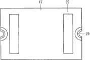
图3A至3C为本发明第二实施例的过电流保护元件的示意图。图3A为过电流保护元件30的立体结构,图3B为图3A中沿2-2剖面线的剖面示意图。图3C为过电流保护元件30的底部视图。过电流保护元件30的基本结构与第一实施例的过电流保护元件10大致相同,不同处在于:导电通孔18以过电流保护元件30两侧面的半圆导电孔25替代。半圆导电孔25的表面可镀上导电层以形成导电连接件29。导电连接件29至少贯穿电极层16、绝缘层15及第一电极箔12,用以电气连接电极层16及第一电极箔12。需注意的是,导电连接件29与第二电极箔14为电气隔离。3A to 3C are schematic diagrams of an overcurrent protection device according to a second embodiment of the present invention. FIG. 3A is a three-dimensional structure of the
上述的导电连接件19、29亦可采用多个或其他型式,而提供等同功效。The above-mentioned
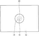
图4A至图4B为本发明第三实施例的过电流保护元件40的示意图。相较于图2A至2C所示的过电流保护元件10的利用电极层16结合外接电极片,且利用焊垫20连接PCM表面,过电流保护元件40类似将元件倒置,利用电极层16以表面黏着或回焊方式连接于PCM表面,而第二电极箔14一般可为铜箔,并可于表面镀锡金属层42,并且利用防焊漆层43(设于元件中央的导电连接件19一端)进行导电连接件19与第二电极箔14及锡金属层42间的电气隔离。锡金属层42可连接外接电极片(图未示),其可连接至电池的电极端。实际上,第二电极箔14和锡金属层42的组合的作用即相当于电极层16,而得以单一铜箔、镍箔、镀镍铜箔或其他金属箔替代。另外,导电连接件19间的空孔可填入绝缘填孔胶41。4A to 4B are schematic diagrams of an
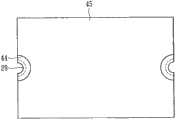
图5A至5B为本发明第四实施例的过电流保护元件50的示意图。相较于图3A至3C所示的过电流保护元件30的利用电极层16结合外接电极片,且利用焊垫20连接PCM表面,过电流保护元件50类似将元件倒置,利用电极层16以表面黏着或回焊方式连接于PCM表面,而第二电极箔14一般可为铜箔,且本实施例是于第二电极箔14表面镀锡金属层45,并且利用防焊漆层44进行导电连接件29与第二电极箔14及锡金属层45间的电气隔离。锡金属层45可以回焊或点焊方式连接外接电极片(图未示),其可连接至电池的电极端。5A to 5B are schematic diagrams of an
图5A及5B的半圆导电连接件29设置于元件两侧,其亦可设置于元件四个角落(1/4圆导电连接件),亦即可采用多个或其他型式的导电连接件,而提供等同功效。The semicircular
按前述实施例的设计,过电流保护元件10、30、40及50一面固定于PCM上,另一面则可连接外接电极片。参照图6A,以过电流保护元件40为例(可以元件10、30、50替代),其固定于PCM 60上,另一端则连接外接电极片61。该外接电极片61一般可为镍片或其他金属片,可连接锂离子或锂高分子电池等二次电池的电极端。外接电极片61可以用回焊或点焊方式与过电流保护元件40或电池的电极结合。According to the designs of the aforementioned embodiments, one side of the
图6A的外接电极片61为长条形,其亦可顺应电池的设计而为各种其它形状,例如图6B的L型,或图6C的弯曲状,以方便连接到电池的电极端。The
传统的PTC元件因无法直接利用点焊与镍片或其他金属片结合,而需以锡膏回焊的方式进行结合,而回焊(reflow)温度常需大于230℃,而恐将影响PTC元件的回复性质。本发明的过电流保护元件焊接外接电极时因可利用点焊,其仅需考虑元件所含的热固性塑胶的固化(curing)温度,其通常小于200℃,而不致于影响PTC元件的回复性质。Traditional PTC components cannot be directly combined with nickel sheets or other metal sheets by spot welding, but need to be combined by solder paste reflow, and the reflow temperature often needs to be higher than 230°C, which may affect PTC components nature of the reply. The overcurrent protection element of the present invention can use spot welding when welding the external electrodes, and it only needs to consider the curing temperature of the thermosetting plastic contained in the element, which is usually less than 200° C., so as not to affect the recovery properties of the PTC element.
本发明的技术内容及技术特点已揭示如上,然而本领域技术人员仍可能基于本发明的教示及揭示而作种种不背离本发明精神的替换及修饰。因此,本发明的保护范围应不限于实施例所揭示的内容,而应包括各种不背离本发明的替换及修饰,并为以下的权利要求范围所涵盖。The technical content and technical features of the present invention have been disclosed above, but those skilled in the art may still make various substitutions and modifications based on the teaching and disclosure of the present invention without departing from the spirit of the present invention. Therefore, the protection scope of the present invention should not be limited to the contents disclosed in the embodiments, but should include various replacements and modifications that do not depart from the present invention, and are covered by the scope of the following claims.
Claims (18)
Priority Applications (1)
| Application Number | Priority Date | Filing Date | Title |
|---|---|---|---|
| CN201110291559.0ACN103021598B (en) | 2011-09-26 | 2011-09-26 | overcurrent protection element |
Applications Claiming Priority (1)
| Application Number | Priority Date | Filing Date | Title |
|---|---|---|---|
| CN201110291559.0ACN103021598B (en) | 2011-09-26 | 2011-09-26 | overcurrent protection element |
Publications (2)
| Publication Number | Publication Date |
|---|---|
| CN103021598Atrue CN103021598A (en) | 2013-04-03 |
| CN103021598B CN103021598B (en) | 2016-05-25 |
Family
ID=47970100
Family Applications (1)
| Application Number | Title | Priority Date | Filing Date |
|---|---|---|---|
| CN201110291559.0AExpired - Fee RelatedCN103021598B (en) | 2011-09-26 | 2011-09-26 | overcurrent protection element |
Country Status (1)
| Country | Link |
|---|---|
| CN (1) | CN103021598B (en) |
Cited By (4)
| Publication number | Priority date | Publication date | Assignee | Title |
|---|---|---|---|---|
| CN106356170A (en)* | 2015-07-16 | 2017-01-25 | 聚鼎科技股份有限公司 | overcurrent protection element |
| CN107527928A (en)* | 2016-06-21 | 2017-12-29 | 胜丽国际股份有限公司 | Optical assembly packaging structure |
| CN108389669A (en)* | 2018-01-26 | 2018-08-10 | 上海神沃电子有限公司 | A kind of preparation method of double-pressure type PTC self- recoverage safety devices |
| CN113614860A (en)* | 2019-04-17 | 2021-11-05 | Koa株式会社 | Current detection resistor |
Citations (5)
| Publication number | Priority date | Publication date | Assignee | Title |
|---|---|---|---|---|
| US20020146547A1 (en)* | 2001-04-06 | 2002-10-10 | Inpaq Technology Co. Ltd. | End electrode structure of surface adhesive over-current protection device and its manufacturing process |
| CN2575817Y (en)* | 2002-08-20 | 2003-09-24 | 聚鼎科技股份有限公司 | overcurrent protection device |
| JP2004172502A (en)* | 2002-11-21 | 2004-06-17 | Hokuriku Electric Ind Co Ltd | Resistor for surface-mounting |
| CN101295570A (en)* | 2007-04-25 | 2008-10-29 | 聚鼎科技股份有限公司 | Protect the circuit board and its overcurrent protection components |
| CN101414499A (en)* | 2007-10-19 | 2009-04-22 | 佳邦科技股份有限公司 | Multi-layer over-current and over-temperature protection structure and manufacturing method thereof |
- 2011
- 2011-09-26CNCN201110291559.0Apatent/CN103021598B/ennot_activeExpired - Fee Related
Patent Citations (5)
| Publication number | Priority date | Publication date | Assignee | Title |
|---|---|---|---|---|
| US20020146547A1 (en)* | 2001-04-06 | 2002-10-10 | Inpaq Technology Co. Ltd. | End electrode structure of surface adhesive over-current protection device and its manufacturing process |
| CN2575817Y (en)* | 2002-08-20 | 2003-09-24 | 聚鼎科技股份有限公司 | overcurrent protection device |
| JP2004172502A (en)* | 2002-11-21 | 2004-06-17 | Hokuriku Electric Ind Co Ltd | Resistor for surface-mounting |
| CN101295570A (en)* | 2007-04-25 | 2008-10-29 | 聚鼎科技股份有限公司 | Protect the circuit board and its overcurrent protection components |
| CN101414499A (en)* | 2007-10-19 | 2009-04-22 | 佳邦科技股份有限公司 | Multi-layer over-current and over-temperature protection structure and manufacturing method thereof |
Cited By (6)
| Publication number | Priority date | Publication date | Assignee | Title |
|---|---|---|---|---|
| CN106356170A (en)* | 2015-07-16 | 2017-01-25 | 聚鼎科技股份有限公司 | overcurrent protection element |
| CN106356170B (en)* | 2015-07-16 | 2019-01-29 | 聚鼎科技股份有限公司 | Overcurrent protection element |
| CN107527928A (en)* | 2016-06-21 | 2017-12-29 | 胜丽国际股份有限公司 | Optical assembly packaging structure |
| CN108389669A (en)* | 2018-01-26 | 2018-08-10 | 上海神沃电子有限公司 | A kind of preparation method of double-pressure type PTC self- recoverage safety devices |
| CN108389669B (en)* | 2018-01-26 | 2019-08-20 | 上海神沃电子有限公司 | A kind of preparation method of double-pressure type PTC self- recoverage safety device |
| CN113614860A (en)* | 2019-04-17 | 2021-11-05 | Koa株式会社 | Current detection resistor |
Also Published As
| Publication number | Publication date |
|---|---|
| CN103021598B (en) | 2016-05-25 |
Similar Documents
| Publication | Publication Date | Title |
|---|---|---|
| TWI503850B (en) | Over-current protection device | |
| CN100461321C (en) | protection element | |
| US7920045B2 (en) | Surface mountable PPTC device with integral weld plate | |
| US8842406B2 (en) | Over-current protection device | |
| US8687336B2 (en) | Over-current protection device and battery protection circuit assembly containing the same | |
| US9019709B2 (en) | Protective circuit module | |
| KR20150135349A (en) | Fuse element and fuse device | |
| US8576043B2 (en) | Surface-mount type overcurrent protection element | |
| CN103021598B (en) | overcurrent protection element | |
| CN205080951U (en) | Overcurrent protection element and protection circuit board thereof | |
| CN202405027U (en) | Overcurrent protection element and battery protection circuit device | |
| CN101295570A (en) | Protect the circuit board and its overcurrent protection components | |
| TWI486988B (en) | Overcurrent protection component and circuit board structure thereof | |
| CN104658726B (en) | Overcurrent protection element and protection circuit board thereof | |
| CN218631538U (en) | Circuit Protection Components | |
| TWI539472B (en) | Over-current protection device | |
| CN216871884U (en) | High-voltage surface-mounted PPTC (polymer positive temperature coefficient) self-recovery fuse with brand-new structure | |
| CN103106989B (en) | Overcurrent protection element and battery protection circuit device | |
| CN205542672U (en) | Surface mount fuse | |
| JP6579687B2 (en) | Electrochemical cell and electrochemical cell module | |
| CN217847574U (en) | Metal oxide varistor device | |
| CN101800102A (en) | Over-current protecting assembly and manufacture method thereof | |
| CN110211852B (en) | High-current fuse with high-heat-conduction substrate and manufacturing method thereof | |
| CN108321060B (en) | Surface mounted fuse and its manufacturing method | |
| CN205810499U (en) | Overcurrent protection assembly |
Legal Events
| Date | Code | Title | Description |
|---|---|---|---|
| C06 | Publication | ||
| PB01 | Publication | ||
| C10 | Entry into substantive examination | ||
| SE01 | Entry into force of request for substantive examination | ||
| C14 | Grant of patent or utility model | ||
| GR01 | Patent grant | ||
| CF01 | Termination of patent right due to non-payment of annual fee | ||
| CF01 | Termination of patent right due to non-payment of annual fee | Granted publication date:20160525 Termination date:20210926 |