CN102983747A - A full-bridge combined soft-switching DC converter - Google Patents
A full-bridge combined soft-switching DC converterDownload PDFInfo
- Publication number
- CN102983747A CN102983747ACN2012105142353ACN201210514235ACN102983747ACN 102983747 ACN102983747 ACN 102983747ACN 2012105142353 ACN2012105142353 ACN 2012105142353ACN 201210514235 ACN201210514235 ACN 201210514235ACN 102983747 ACN102983747 ACN 102983747A
- Authority
- CN
- China
- Prior art keywords
- parallel
- circuit
- full
- buffer circuit
- voltage
- Prior art date
- Legal status (The legal status is an assumption and is not a legal conclusion. Google has not performed a legal analysis and makes no representation as to the accuracy of the status listed.)
- Pending
Links
- 239000003990capacitorSubstances0.000claimsabstractdescription25
- 230000003071parasitic effectEffects0.000claimsdescription6
- 238000011084recoveryMethods0.000claimsdescription6
- 238000004804windingMethods0.000claimsdescription6
- 238000005516engineering processMethods0.000abstractdescription14
- 238000010586diagramMethods0.000description14
- 238000013461designMethods0.000description7
- 230000008859changeEffects0.000description4
- 238000011161developmentMethods0.000description4
- 241001270131Agaricus moelleriSpecies0.000description3
- 238000000034methodMethods0.000description3
- 230000015556catabolic processEffects0.000description2
- 230000014509gene expressionEffects0.000description2
- 230000006872improvementEffects0.000description2
- XEEYBQQBJWHFJM-UHFFFAOYSA-NIronChemical group[Fe]XEEYBQQBJWHFJM-UHFFFAOYSA-N0.000description1
- 238000010521absorption reactionMethods0.000description1
- 230000009286beneficial effectEffects0.000description1
- 239000004568cementSubstances0.000description1
- 230000005284excitationEffects0.000description1
- 230000001939inductive effectEffects0.000description1
- 239000000463materialSubstances0.000description1
- 238000005457optimizationMethods0.000description1
- 230000008569processEffects0.000description1
- 238000012545processingMethods0.000description1
- 230000009467reductionEffects0.000description1
- 238000011160researchMethods0.000description1
- 229920006395saturated elastomerPolymers0.000description1
- 229910000859α-FeInorganic materials0.000description1
Images


Classifications
- Y—GENERAL TAGGING OF NEW TECHNOLOGICAL DEVELOPMENTS; GENERAL TAGGING OF CROSS-SECTIONAL TECHNOLOGIES SPANNING OVER SEVERAL SECTIONS OF THE IPC; TECHNICAL SUBJECTS COVERED BY FORMER USPC CROSS-REFERENCE ART COLLECTIONS [XRACs] AND DIGESTS
- Y02—TECHNOLOGIES OR APPLICATIONS FOR MITIGATION OR ADAPTATION AGAINST CLIMATE CHANGE
- Y02B—CLIMATE CHANGE MITIGATION TECHNOLOGIES RELATED TO BUILDINGS, e.g. HOUSING, HOUSE APPLIANCES OR RELATED END-USER APPLICATIONS
- Y02B70/00—Technologies for an efficient end-user side electric power management and consumption
- Y02B70/10—Technologies improving the efficiency by using switched-mode power supplies [SMPS], i.e. efficient power electronics conversion e.g. power factor correction or reduction of losses in power supplies or efficient standby modes
Landscapes
- Dc-Dc Converters (AREA)
- Inverter Devices (AREA)
Abstract
Translated fromChinese
Description
Translated fromChinese技术领域technical field
本发明涉及一种全桥组合软开关直流变换器,属于电力电子技术领域。The invention relates to a full-bridge combined soft-switching DC converter, which belongs to the technical field of power electronics.
背景技术Background technique
通常,功率变换器是一种将输入电压源或电流源变换成指定输出电压或电流的功率处理电路。Generally, a power converter is a power processing circuit that transforms an input voltage or current source into a specified output voltage or current.
功率变换器的一种类型,即基于全桥拓扑的DC/DC功率变换器,是大、中功率DC/DC变换器的理想电路,得到广泛的应用和研究。全桥变换器主要包括全桥逆变电路、高频变压器和输出整流滤波电路组成,具有功率开关器件电压、电流额定值较小,功率变压器利用率较高等明显优点。One type of power converter, the DC/DC power converter based on the full-bridge topology, is an ideal circuit for large and medium power DC/DC converters, and has been widely used and researched. The full-bridge converter mainly consists of a full-bridge inverter circuit, a high-frequency transformer, and an output rectification filter circuit. It has obvious advantages such as low voltage and current ratings of power switching devices, and high utilization of power transformers.
大电流快速IGBT和大电流快速恢复二极管技术的发展使得大、中功率变换器得以实现。而传统的PWM全桥变换器,由于开关管工作在硬开关状态,开关损耗和开关噪声大,因而影响了效率和开关频率的提高,从而制约了功率变换器的功率密度的提高和单位输出功率的体积和重量的减小。因此,人们提出了软开关技术。软开关分为零电压开关和零电流开关。目前,软开关技术主要有两种发展方向:一个方向是附加开关或改变主电路拓扑等形式,一般是在变换器电路中设置某种形式的LC谐振电路,这使得输入滤波器和输出滤波器的设计复杂化,并影响系统的噪声。另一个发展方向是无损(低损)缓冲吸收电路,其基本思路是设计一容性支路与开关管并联,一感性支路与开关管串联,处理吸收储存元件中的能量,将其回馈至电源或大幅消减其数值,从而消除(消弱)损耗问题,达到软化开关的目的。如今软开关变换器都应用了谐振原理,在电路中并联或串联谐振网络,势必产生谐振损耗,并使电路受到固有问题的影响。为此,人们在谐振技术和无损耗缓冲电路的基础上提出了组合软开关功率变换器的理论。组合软开关技术结合了无损耗吸收技术与谐振式零电压技术、零电流技术的优点。电路中既可以存在零电压开通,也可以存在零电流关断,同时既可以包含零电流开通,也可以包含零电压关断,是这四种状态的任意组合。由此可见,由无损耗缓冲技术和谐振技术组合而成的新型软开关技术将成为新的发展趋势。到现在,对软开关的研究取得了很大的进展,然而还未实现软开关技术的实用化。The development of high-current fast IGBT and high-current fast recovery diode technology enables the realization of large and medium power converters. In the traditional PWM full-bridge converter, because the switching tube works in a hard switching state, the switching loss and switching noise are large, which affects the efficiency and the improvement of the switching frequency, thus restricting the improvement of the power density of the power converter and the unit output power. reduction in size and weight. Therefore, people have proposed soft switching technology. Soft switching is divided into zero voltage switching and zero current switching. At present, there are two main development directions of soft switching technology: one direction is to add switches or change the topology of the main circuit. Generally, some form of LC resonant circuit is set in the converter circuit, which makes the input filter and output filter complicates the design and affects system noise. Another development direction is the lossless (low loss) snubbing circuit. The basic idea is to design a capacitive branch in parallel with the switch tube, and an inductive branch in series with the switch tube to process and absorb the energy in the storage element and feed it back to the The value of the power supply may be greatly reduced to eliminate (weaken) the loss problem and achieve the purpose of softening the switch. Nowadays, the soft switching converters all use the resonance principle, and the parallel or series resonant network in the circuit will inevitably produce resonance loss and make the circuit affected by inherent problems. For this reason, people put forward the theory of combined soft-switching power converter on the basis of resonant technology and lossless snubber circuit. Combined soft switching technology combines the advantages of lossless absorption technology, resonant zero voltage technology and zero current technology. There can be both zero-voltage turn-on and zero-current turn-off in the circuit, and it can contain both zero-current turn-on and zero-voltage turn-off, which is any combination of these four states. It can be seen that the new soft switching technology composed of lossless buffer technology and resonance technology will become a new development trend. Up to now, the research on soft switching has made great progress, but the practical application of soft switching technology has not yet been realized.
全桥变换器中,两个桥臂的导通时间不相同、开关管的导通压降存在略微的差异、每个导通管的储存时间不同等都会造成初级置位伏秒数与复位伏秒数不相等。只要伏秒数稍有不等,磁芯就不能回到起点,并且若干周期后,磁芯将偏离磁滞回线进入饱和区。磁芯饱和时,变压器不能承受电压,当下一周期开关管再次导通时,开关管将承受很大的电压和电流,导致开关管损坏。In a full-bridge converter, the conduction time of the two bridge arms is different, the conduction voltage drop of the switch tube is slightly different, and the storage time of each conduction tube is different. The seconds are not equal. As long as the volt-seconds are slightly different, the core cannot return to the starting point, and after a few cycles, the core will deviate from the hysteresis loop and enter the saturation region. When the magnetic core is saturated, the transformer cannot withstand the voltage. When the switch tube is turned on again in the next cycle, the switch tube will bear a large voltage and current, resulting in damage to the switch tube.
发明内容Contents of the invention
为了克服上述的不足,本发明的目的在于提供一种全桥组合软开关直流变换器。In order to overcome the above disadvantages, the object of the present invention is to provide a full-bridge combined soft-switching DC converter.
本发明采取的技术方案:The technical scheme that the present invention takes:
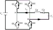
一种全桥组合软开关直流变换器,包括逆变电路、串联谐振电路、高频变压器、输出整流电路、输出滤波电路;A full-bridge combined soft-switching DC converter, including an inverter circuit, a series resonant circuit, a high-frequency transformer, an output rectifier circuit, and an output filter circuit;
所述逆变电路包括4个IGBT管Q1、Q2、Q3和Q4,4个IGBT管的寄生二极管D11、D22、D33和D44;The inverter circuit includes four IGBT tubes Q1, Q2, Q3 and Q4, and parasitic diodes D11, D22, D33 and D44 of the four IGBT tubes;
Q1和Q3的公共端与高频变压器的初级绕组的一端之间有串联谐振电路,Q2和Q4的公共端与高频变压器初级绕组的另一端连接,Q1两端并联RCD缓冲电路I,Q2两端并联RCD缓冲电路II,Q3两端并联RCD缓冲电路III,Q4两端并联RCD缓冲电路IV;高频变压器输出端连接输出整流电路,输出整流电路连接输出滤波电路。There is a series resonant circuit between the common end of Q1 and Q3 and one end of the primary winding of the high-frequency transformer, the common end of Q2 and Q4 is connected to the other end of the primary winding of the high-frequency transformer, and the RCD snubber circuit I and Q2 are connected in parallel at both ends of Q1 RCD snubber circuit II is connected in parallel at both ends of Q3, RCD snubber circuit III is connected in parallel at both ends of Q4, and RCD snubber circuit IV is connected in parallel at both ends of Q4; the output end of the high-frequency transformer is connected with the output rectification circuit, and the output rectification circuit is connected with the output filter circuit.
RCD缓冲电路I由C1、D1和R1组成,C1与D1串联后与Q1并联,所述D1上并联有R1;RCD缓冲电路II由C2、D2和R2组成,C2与D2串联后与Q2并联,所述D2上并联有R2;RCD缓冲电路III由C3、D3和R3组成,C3与D3串联后与Q3并联,所述D3上并联有R3;RCD缓冲电路IV由C4、D4和R4组成,C4与D4串联后与Q4并联,所述D4上并联有R4。RCD snubber circuit I is composed of C1, D1 and R1, C1 and D1 are connected in parallel with Q1 after being connected in series, and R1 is connected in parallel with D1; RCD snubber circuit II is composed of C2, D2 and R2, C2 and D2 are connected in series and then connected in parallel with Q2, R2 is connected in parallel on the D2; RCD snubber circuit III is composed of C3, D3 and R3, C3 and D3 are connected in parallel with Q3, and R3 is connected in parallel on the D3; RCD snubber circuit IV is composed of C4, D4 and R4, and C4 After being connected in series with D4, it is connected in parallel with Q4, and R4 is connected in parallel with D4.
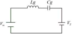
串联谐振电路由谐振电感Lg和谐振电容Cg串联构成。The series resonant circuit is composed of a resonant inductor Lg and a resonant capacitor Cg connected in series.
高频变压器的次级绕组的一端与整流二极管D5和D7的公共端连接,另一端与整流二极管D6和D8的公共端连接。One end of the secondary winding of the high frequency transformer is connected to the common end of the rectifying diodes D5 and D7, and the other end is connected to the common end of the rectifying diodes D6 and D8.
所述输出整流电路包括4个快恢复二极管D5、D6、D7和D8,D5两端并联RC缓冲电路I,D6两端并联RC缓冲电路II,D7两端并联RC缓冲电路III,D8两端并联RC缓冲电路IV;所述RC缓冲电路I由R5及C5串联构成,RC缓冲电路II由R6及C6串联构成,RC缓冲电路III由R7及C7串联构成,RC缓冲电路IV由R8及C8串联构成。The output rectification circuit includes four fast recovery diodes D5, D6, D7 and D8, the two ends of D5 are connected in parallel with RC snubber circuit I, the two ends of D6 are connected in parallel with RC snubber circuit II, the two ends of D7 are connected in parallel with RC snubber circuit III, and the two ends of D8 are connected in parallel RC snubber circuit IV; the RC snubber circuit I is composed of R5 and C5 in series, RC snubber circuit II is composed of R6 and C6 in series, RC snubber circuit III is composed of R7 and C7 in series, and RC snubber circuit IV is composed of R8 and C8 in series .
所述输出滤波电路包括电感L和电解电容Co1和Co2,Co1与Co2的电容值相等,电阻Ro1和Ro2分别与Co1和Co2并联,电阻Ro1和Ro2的阻值相等,所述的Co1和Co2的工作电压相等;Co3和Co4为无极性电容,Co3和Co4分别与Co1和Co2并联。The output filter circuit includes an inductance L and electrolytic capacitors Co1 and Co2, the capacitance values of Co1 and Co2 are equal, the resistances Ro1 and Ro2 are connected in parallel with Co1 and Co2 respectively, the resistance values of the resistances Ro1 and Ro2 are equal, and the resistance values of the Co1 and Co2 The working voltage is equal; Co3 and Co4 are non-polar capacitors, and Co3 and Co4 are connected in parallel with Co1 and Co2 respectively.
所述为输入端的直流电压经过所述逆变电路逆变成高频的交流方波电压,所述Q1和Q4为一对导通管,Q1和Q4同时导通或Q1和Q4同时关断;Q2和Q3为另一对导通管,Q2和Q3同时导通或Q2和Q3同时关断;同一桥臂的两个IGBT管不能同时导通,每一对导通管的占空比在输入电压最低时不大于95%。The DC voltage at the input end is converted into a high-frequency AC square wave voltage through the inverter circuit, and the Q1 and Q4 are a pair of conduction tubes, and Q1 and Q4 are turned on at the same time or Q1 and Q4 are turned off at the same time; Q2 and Q3 are another pair of conduction transistors. Q2 and Q3 are turned on at the same time or Q2 and Q3 are turned off at the same time; The lowest voltage is not more than 95%.
本发明的原理:一种全桥拓扑组合软开关直流变换器,输入的直流电源经过输入滤波电路供给全桥逆变电路,由Q1、Q2、Q3和Q4四个开关管组成的桥式逆变电路将直流电逆变成高频的交流方波电压,再经过高频变压器变压后整流滤波,最后输出稳定的直流电压;设计开关管缓冲电路,使得开关管关断时集电极电压缓慢上升,减少开关损耗;能抑制了漏感尖峰,防止二次击穿,可以选择较低耐压值的开关管,降低了成本,提高了变换器的可靠性;串联谐振电路的谐振频率等于开关频率,使得逆变之后的电压为准正弦波交流电压。The principle of the present invention: a full-bridge topology combined soft-switching DC converter, the input DC power is supplied to the full-bridge inverter circuit through the input filter circuit, and the bridge inverter is composed of four switch tubes Q1, Q2, Q3 and Q4 The circuit inverts the DC power into a high-frequency AC square wave voltage, and then rectifies and filters it after being transformed by a high-frequency transformer, and finally outputs a stable DC voltage; the switch tube buffer circuit is designed so that the collector voltage rises slowly when the switch tube is turned off. Reduce switching loss; it can suppress the leakage inductance peak and prevent secondary breakdown. You can choose a switch tube with a lower withstand voltage value, which reduces the cost and improves the reliability of the converter; the resonant frequency of the series resonant circuit is equal to the switching frequency. Make the voltage after inversion a quasi-sine wave AC voltage.
本发明的有益效果:本发明全桥组合软开关直流变换器采用RCD缓冲电路和串联谐振电路的组合软开关技术,真正减小了开关损耗,且能有效解决全桥直流变换器的偏磁问题,占空比丢失低。该实施方案不需外加辅助开关,电路结构简单,实现简单。开关管的工作频率恒定,因为是恒频方式控制,所以软开关的实现条件不依耐输入电压和输出电流等外部条件,有利于高频变压器实现高功率密度和高效率。简化了功率变压器、输入和输出滤波器的设计。Beneficial effects of the present invention: The full-bridge combined soft-switching DC converter of the present invention adopts the combined soft-switching technology of the RCD snubber circuit and the series resonant circuit, which really reduces the switching loss and can effectively solve the magnetic bias problem of the full-bridge DC converter , the duty cycle is lost low. This implementation scheme does not need an additional auxiliary switch, the circuit structure is simple, and the realization is simple. The operating frequency of the switching tube is constant. Because it is controlled by a constant frequency method, the realization conditions of soft switching do not depend on external conditions such as input voltage and output current, which is conducive to high-frequency transformers to achieve high power density and high efficiency. Simplifies the design of power transformers, input and output filters.
附图说明Description of drawings
图1是本发明电路结构简图。Fig. 1 is a schematic diagram of the circuit structure of the present invention.
图2是本发明实施例的IGBT(Q1)两端无RCD缓冲电路时集电极和发射极之间的电压和流过Q1的电流波形示意图。Fig. 2 is a schematic diagram of the voltage between the collector and the emitter and the current waveform flowing through Q1 when there is no RCD snubber circuit at both ends of the IGBT (Q1) according to the embodiment of the present invention.
图3是本发明实施例的IGBT(Q1)两端并联RCD缓冲电路时集电极和发射极之间的电压波形示意图。Fig. 3 is a schematic diagram of the voltage waveform between the collector and the emitter when both ends of the IGBT (Q1) are connected in parallel with an RCD snubber circuit according to an embodiment of the present invention.
图4是本发明实施例的全桥组合软开关直流变换器的主要波形示意图。FIG. 4 is a schematic diagram of main waveforms of a full-bridge combined soft-switching DC converter according to an embodiment of the present invention.
图5是本发明实施例的全桥组合软开关直流变换器各开关模态1[t′0,t′1]等效电路结构示意图。Fig. 5 is a schematic structural diagram of the equivalent circuit structure of each switching mode 1 [t′0 , t′1 ] of the full-bridge combined soft-switching DC converter according to the embodiment of the present invention.
图6是本发明实施例的全桥组合软开关直流变换器各开关模态2[t′1,t′2]等效电路结构示意图。Fig. 6 is a schematic structural diagram of the equivalent circuit structure of each switching mode 2 [t′1 , t′2 ] of the full-bridge combined soft-switching DC converter according to the embodiment of the present invention.
图7是本发明实施例的全桥组合软开关直流变换器各开关模态3[t′2,t′3]等效电路结构示意图。Fig. 7 is a schematic structural diagram of the equivalent circuit structure of each switching mode 3 [t′2 , t′3 ] of the full-bridge combined soft-switching DC converter according to the embodiment of the present invention.
图8是本发明实施例的全桥组合软开关直流变换器各开关模态4[t′3,t′4]等效电路结构示意图。Fig. 8 is a schematic structural diagram of the equivalent circuit structure of each switching mode 4 [t′3 , t′4 ] of the full-bridge combined soft-switching DC converter according to the embodiment of the present invention.
图9是本发明实施例的全桥组合软开关直流变换器的不同开关模态的统一等效电路图。FIG. 9 is a unified equivalent circuit diagram of different switching modes of the full-bridge combined soft-switching DC converter according to the embodiment of the present invention.
图中:1逆变电路,2串联谐振电路,3高频变压器,4输出整流电路,5输出滤波电路。In the figure: 1 inverter circuit, 2 series resonant circuit, 3 high frequency transformer, 4 output rectifier circuit, 5 output filter circuit.
具体实施方式Detailed ways
如图1所示为本发明实施例的电路结构简图。本发明包括逆变电路(1)、串联谐振电路(2)、高频变压器(3)、输出整流电路(4)、输出滤波电路(5)。FIG. 1 is a schematic diagram of the circuit structure of the embodiment of the present invention. The invention includes an inverter circuit (1), a series resonant circuit (2), a high-frequency transformer (3), an output rectification circuit (4), and an output filter circuit (5).
如图2所示为本发明实施例的IGBT(Q1)两端无RCD缓冲电路I时集电极和发射极之间的电压和流过Q1的电流波形示意图。当Q1开通期间,Q4开通,Q2和Q3关断,Q1两端的电压为0V;t1时刻,Q1和Q4关断,此时储存在所述高频变压器励磁电感中的能量释放,电感两端电压极性反向,使Q1的集电极电压迅速上升到所述输入电压Vin,由于所述高频变压器存在漏感,漏感中的能量也释放,所以Q1集电极产生漏感尖峰电压VL,所述漏感尖峰电压VL大于所述电压Vin,然后电压又在关断时间tf结束时下降到在Q1关断瞬间到关断结束的tf时间内,流过Q1的电流从最初峰值电流Ip下降到0A;t1~t2:Q1和Q4关断,Q2和Q3仍然处于关断状态,Q1两端的电压为流过Q1的电流为0A;t2时刻,Q2和Q3开通,Q1两端的电压上升到Vin;t2~t3:Q1和Q4保持关断,Q2和Q3保持开通,Q1两端的电压为Vin,流过Q1的电流为0A;t3时刻,Q2和Q3关断,在Q2和Q3上产生漏感尖峰VL,Q1两端的电压为Vl,Vl=Vin-VL(<0);t3~t4:Q1和Q4保持关断,Q2和Q3处于关断状态,Q1两端的电压为流过Q1的电流仍为0A;t4时刻,Q1和Q4开通,Q1两端的电压为0V,由于所述高频变压器电感和谐振电感的存在,使得流过Q1的电流缓慢上升到Iin;t4~t5:Q1和Q4保持开通,Q1两端的电压为0V,流过Q1的电流从Iin上升到Ip。FIG. 2 is a schematic diagram of the voltage between the collector and the emitter and the current waveform flowing through Q1 when there is no RCD snubber circuit I at both ends of the IGBT (Q1) according to the embodiment of the present invention. When Q1 is turned on, Q4 is turned on, Q2 and Q3 are turned off, and the voltage across Q1 is 0V; at timet1 , Q1 and Q4 are turned off, and the energy stored in the high-frequency transformer excitation inductance is released at this time, and the two ends of the inductance The polarity of the voltage is reversed, so that the collector voltage of Q1 rises rapidly to the input voltage Vin , and because the high-frequency transformer has leakage inductance, the energy in the leakage inductance is also released, so the collector of Q1 generates a leakage inductance peak voltage VL , the leakage inductance spike voltage VL is greater than the voltage Vin , and then thevoltage drops to During the time tf from the moment Q1 is turned off to the end of the turn-off, the current flowing through Q1 drops from the initial peak current Ip to 0A; t1 ~ t2 : Q1 and Q4 are turned off, and Q2 and Q3 are still in the off state , the voltage across Q1 is The current flowing through Q1 is 0A; at time t2 , Q2 and Q3 are turned on, and the voltage across Q1 rises to Vin ; t2 ~ t3 : Q1 and Q4 keep off, Q2 and Q3 keep on, and the voltage across Q1 is Vin , the current flowing through Q1 is 0A; at timet3 , Q2 and Q3 are turned off, and a leakage inductance peak VL is generated on Q2 and Q3, and the voltage across Q1 is Vl , Vl =Vin -VL ( <0); t3 ~t4 : Q1 and Q4 keep off, Q2 and Q3 are in the off state, the voltage across Q1 is The current flowing through Q1 is still 0A; at timet4 , Q1 and Q4 are turned on, and the voltage across Q1 is 0V. Due to the existence of the high-frequency transformer inductance and resonant inductance, the current flowing through Q1 slowly rises to Iin ; t4 ~t5 : Q1 and Q4 are kept on, the voltage across Q1 is 0V, and the current flowing through Q1 rises from Iin to Ip .
为了抑制漏感尖峰电压VL,减小所述开关管IGBT关断时的重叠损耗,防止所述开关管IGBT关断瞬间在其集电极和发射极之间产生很高的电压尖峰,在开关管IGBT两端设计所述RCD缓冲电路。In order to suppress the leakage inductance peak voltage VL , reduce the overlap loss when the switching tube IGBT is turned off, and prevent the high voltage spike between the collector and the emitter of the switching tube IGBT when the switching tube IGBT is turned off, the switch Design the RCD snubber circuit at both ends of the tube IGBT.
如图3所示为本发明实施例IGBT(Q1)两端并联RCD缓冲电路I时集电极和发射极之间的电压波形示意图。在t1时刻,Q1关断(即Q1和Q4关断),由于一部分电流通过二极管D1给C1充电,使得在Q1的关断时间tf内,Q1两端的电压不会瞬间上升到VL,而是缓慢上升到小于VL的电压Vp,当Q1完全关断后,C1两端的电压通过电阻R1放电到t2时刻;在t2时刻,Q1两端的电压缓慢上升到Vin;t3时刻,Q2和Q3关断,Q1两端的电压缓慢下降,当Q2和Q3完全关断后,Q1两端的电压又缓慢上升;t4时刻,Q1和Q4开通,Q1两端的缓慢下降到0V。FIG. 3 is a schematic diagram of the voltage waveform between the collector and the emitter when both ends of the IGBT (Q1) are connected in parallel with the RCD snubber circuit I according to the embodiment of the present invention. At timet1 , Q1 is turned off (that is, Q1 and Q4 are turned off), and because a part of the current is charged to C1 through diode D1, the voltage at both ends of Q1 will not rise to VL instantaneously during the off time tf of Q1. Instead, it rises slowly to a voltage Vp that is less than VL. When Q1 is completely turned off, the voltage across C1 discharges through the resistor R1 to time t2 ; at time t2 , the voltage across Q1 slowly rises to Vin ; t3 At timet4 , Q1 and Q4 are turned on, and the voltage across Q1 slowly drops to 0V when Q2 and Q3 are completely turned off.
假设最初的峰值电流Ip流过C1的电流为Ip/2,流过逐渐关断的Q1的电流为Ip/2。设计合适的电容C1,使得两端的电压在Q1的关断时间tf内上升到2Vdc。则C1和R1的表达式推导如下:Assume that the initial peak currentIp flows through C1 asIp /2, and the current flowing through Q1 as it gradually turns off isIp /2. Properly design the capacitor C1 so that the voltage across it rises to 2Vdc within the off time tf of Q1. Then the expressions of C1 and R1 are derived as follows:
(1)输入功率为Pin,输出额定功率Po,变换器的效率为η;(1) The input power is Pin , the output rated power is Po , and the efficiency of the converter is η;
(2)Vin的最小电压为Vin(min),开关管的占空比为D,开关周期为T;(2) The minimum voltage of Vin is Vin(min) , the duty cycle of the switching tube is D, and the switching period is T;
如图2所示,流过Q1的电流脉冲是一个宽度为

由电容元件的电压电流关系(VCR)得:From the voltage-current relationship (VCR) of the capacitive element:
式2带入式3得
由于在Q1下一次关断的开始时刻,C1两端应保证没有电压,因此图3中,在t1+tf时刻到t5时刻之间的时间内,C1必须放电完成。当Q1在t4时刻开始导通时,C1通过Q1和R1构成放电回路。R1应使C1在1/10的最小导通时间ton(min)(t4至t5)内放电至所充电荷的5%以下。得到C1和R1的关系为:Since there should be no voltage at both ends of C1 at the beginning of the next turn-off of Q1, in Figure 3, C1 must be fully discharged during the time between t1 +tf and t5 . When Q1 starts conducting att4 , C1 forms a discharge circuit through Q1 and R1. R1 should make C1 discharge to less than 5% of the charged charge within 1/10 of the minimum on-time ton(min) (t4 to t5 ). The relationship between C1 and R1 is obtained as:
C1=C2=C3=C4;R1=R2=R3=R4。C1=C2=C3=C4; R1=R2=R3=R4.
如图4所示为本发明实施例的全桥拓扑直流变换器的时序和主要波形示意图。图4从上至下的波形分别为:全桥逆变电路中开关管Q1、Q4的驱动电压VGS(Q1,Q4)的波形;全桥逆变电路中开关管Q2、Q3的驱动电压VGS(Q2,Q3)的波形;全桥逆变电路逆变后的电压VAB的波形;高频变压器T原边的电压VT的波形;流过谐振电感Lg的电流
本发明实施例的全桥拓扑直流变换器的开关频率为f,串联谐振电路谐振频率为fg。当fg=f时,由图5可知,全桥拓扑直流变换器在一个开关周期内有可分为4种开关模式,分别是[t′0,t′1]、[t′1,t′2]、[t′2,t′3]、[t′3,t′4]。以下简要介绍各种工作模态的工作原理。The switching frequency of the full-bridge topology DC converter in the embodiment of the present invention is f, and the resonant frequency of the series resonant circuit is fg . When fg =f, it can be seen from Figure 5 that the full-bridge topology DC converter can be divided into four switching modes in one switching cycle, which are [t′0 , t′1 ], [t′1 , t '2 ], [t'2 , t'3 ], [t'3 , t'4 ]. The working principles of various working modes are briefly introduced below.
开关模态1[t′0,t′1]如图5所示:The switching mode 1[t′0 , t′1 ] is shown in Fig. 5:
由于开关频率f=fg和死区时间短,在t′0时刻之前的死区时间内,谐振电感电流iLg很小,流过二极管D22、D33,谐振电容电压为负。在t′0时刻,Q1、Q4开通,D22、D33立即截止,存在很小的反向恢复电流,此电流流过Q1、Q4,在Q1、Q4中产生很小的开通电流尖峰,Q1、Q4的开通损耗很小,因此Q1、Q4是软开通。在[t′0,t′1]模态期间,谐振电感电流iLg和谐振电容电压vCg近似正弦波变化,在t′1时刻,谐振电感电流iLg=0,谐振电容电压最大,Q1、Q4关断,Q1、Q4的寄生二极管D11、D44将Q1、Q4两端的电压箝在零位,Q1、Q4零电压/零电流关断。Because the switching frequency f=fg and the dead time is short, the resonant inductor current iLg is very small during the dead time before t′0 , and flows through the diodes D22 and D33, and the voltage of the resonant capacitor is negative. At time t′0 , Q1 and Q4 are turned on, D22 and D33 are turned off immediately, and there is a small reverse recovery current, which flows through Q1 and Q4, and a small turn-on current peak is generated in Q1 and Q4, and Q1 and Q4 The turn-on loss is very small, so Q1 and Q4 are soft turn-on. During the [t′0 , t′1 ] mode, the resonant inductor current iLg and the resonant capacitor voltage vCg change approximately sinusoidally. At t′1 moment, the resonant inductor current iLg = 0, and the resonant capacitor voltage is the largest, Q1 , Q4 is turned off, the parasitic diodes D11 and D44 of Q1 and Q4 clamp the voltage across Q1 and Q4 at zero, and Q1 and Q4 are turned off with zero voltage/zero current.
开关模态2[t′1,t′2]如图6所示:The switching mode 2[t′1 , t′2 ] is shown in Fig. 6:
在此开关模态中,iLg反方向流动,Q1、Q4的寄生二极管D11、D44导通,谐振电容Cg开始放电,但由于开关模态2时间很短,所以iLg方向的增加量小。In this switching mode, iLg flows in the opposite direction, the parasitic diodes D11 and D44 of Q1 and Q4 are turned on, and the resonant capacitor Cg starts to discharge, but because the time of switching
开关模态3[t′2,t′3]如图7所示:The switching mode 3[t′2 , t′3 ] is shown in Fig. 7:
由于开关频率f=fg和死区时间短,在t′2时刻之前的死区时间内,谐振电感电流iLg很小,流过二极管D11、D44,谐振电容电压为正。在t′2时刻,Q2、Q3开通,D11、D44立即截止,存在很小的反向恢复电流,此电流流过Q2、Q3,在Q2、Q3中产生很小的开通电流尖峰,Q2、Q3的开通损耗很小,因此Q2、Q3是软开通。在[t′2,t′3]模态期间,谐振电感电流iLg和谐振电容电压vCg近似正弦波变化,在t′3时刻,谐振电感电流iLg=0,谐振电容电压最大,Q2、Q3关断,Q2、Q3的寄生二极管D22、D33将Q2、Q3两端的电压箝在零位,Q2、Q3零电压/零电流关断。Because the switching frequency f=fg and the dead time is short, the resonant inductor current iLg is very small in the dead time before the moment t′2 , flows through the diodes D11 and D44, and the voltage of the resonant capacitor is positive. At timet′2 , Q2 and Q3 are turned on, D11 and D44 are turned off immediately, there is a small reverse recovery current, this current flows through Q2 and Q3, and a small turn-on current peak is generated in Q2 and Q3, Q2 and Q3 The turn-on loss is very small, so Q2 and Q3 are soft turn-on. During the [t′2 , t′3 ] mode, the resonant inductor current iLg and the resonant capacitor voltage vCg change approximately sinusoidally. At t′3 , the resonant inductor current iLg = 0, and the resonant capacitor voltage is the largest, Q2 , Q3 is turned off, the parasitic diodes D22 and D33 of Q2 and Q3 clamp the voltage across Q2 and Q3 at zero, and Q2 and Q3 are turned off with zero voltage/zero current.
开关模态4[t′3,t′4]如图8所示:The switching mode 4[t′3 , t′4 ] is shown in Fig. 8:
在此开关模态中,iLg反方向流动,Q2、Q3的寄生二极管D22、D33导通,谐振电容Cg开始放电,但由于开关模态4时间很短,所以iLg方向的增加量小。In this switching mode, iLg flows in the opposite direction, the parasitic diodes D22 and D33 of Q2 and Q3 are turned on, and the resonant capacitor Cg starts to discharge, but because the time of switching mode 4 is very short, the increase in the direction of iLg is small.
有以上分析可知,选择合适的谐振电感和谐振电容使谐振电容使得谐振频率等于开关频率,开关管Q1、Q2、Q3和Q4很容易实现ZCS开通和ZCS/ZVS关断。由于高频变压器漏感Lt的存在,谐振电感量等于谐振电感Lg和变压器漏感Lt之和。以下推导谐振电感Lg和谐振电容Cg的表达式。From the above analysis, it can be known that selecting the appropriate resonant inductance and resonant capacitor makes the resonant capacitor make the resonant frequency equal to the switching frequency, and the switching tubes Q1, Q2, Q3 and Q4 can easily realize ZCS turn-on and ZCS/ZVS turn-off. Due to the existence of the high-frequency transformer leakage inductance Lt, the resonant inductance is equal to the sum of the resonant inductance Lg and the transformer leakage inductance Lt. The expressions of the resonance inductance Lg and the resonance capacitance Cg are derived below.
如图5所示,谐振电容Cg两端的充电电压vCg使高频变压器T的初级平顶脉冲电压VT有所下降,使变压器次级电压降低,获得同样输出电压所需的开关管导通时间延长,一般希望初级脉冲电压尽可能保持平波。设计平顶脉冲电压允许的下降量为10%。谐振电容Cg公式推导如下:As shown in Figure 5, the charging voltage vCg at both ends of the resonant capacitor Cg reduces the primary flat-top pulse voltage VT of the high-frequency transformer T, reduces the secondary voltage of the transformer, and turns on the switch tube required to obtain the same output voltage When the time is extended, it is generally hoped that the primary pulse voltage can be kept as flat as possible. The allowable drop of the designed flat-top pulse voltage is 10%. The resonant capacitance Cg formula is derived as follows:
(1)开关管在一个周期内的开通时间为ton;(1) the turn-on time of the switch tube in one cycle is ton ;
(2)输入直流电流为Iin;(2) input direct current is Iin ;
如图9所示为是本发明实施例的全桥拓扑直流变换器的不同开关模态的统一等效电路图。FIG. 9 is a unified equivalent circuit diagram of different switching modes of the full-bridge topology DC converter according to the embodiment of the present invention.
由谐振电路原理得:According to the principle of resonant circuit:
fg=f带入上式得fg = f into the above formula to get
本发明实施例的具体参数如下:设定开关频率为20KHz,输入电压是蓄电池提供的DC240V,输出电压DC600V,输出电流16.7A;输入滤波电容Cia为1000uF/450V,Cib为0.22uF/400V;全桥逆变电路的开关管Q1、Q2、Q3和Q4选用SKM100GB12V,电容C1、C2、C3和C4为3300uF/2500V,吸收电阻R1、R2、R3和R4为680Ω/10W水泥电阻,二极管D1、D2、D3和D4选用肖特基二极管IN5408;谐振电容Cg为40uF/800V.DC60A的MKP-C电容,谐振电感Lg为1.5uH;高频变压器原边的匝数为14匝,副边的匝数为51匝,铁芯选用EE型铁芯EE110/56/36,材料为铁氧体;整流二极管D5、D6、D7和D8选用快速回复二极管DSEI 2X101;输出滤波电感L为2.5mH,输出滤波电容Co1、Co2为1000uF/450V,Co3、Co4为0.22uF/400V;Ro1、Ro2为680K的膜电阻。The specific parameters of the embodiment of the present invention are as follows: the switching frequency is set to 20KHz, the input voltage is DC240V provided by the battery, the output voltage is DC600V, and the output current is 16.7A; the input filter capacitor Cia is 1000uF/450V, and Cib is 0.22uF/400V; The switching tubes Q1, Q2, Q3 and Q4 of the bridge inverter circuit use SKM100GB12V, the capacitors C1, C2, C3 and C4 are 3300uF/2500V, the absorbing resistors R1, R2, R3 and R4 are 680Ω/10W cement resistors, and the diodes D1 and D2 , D3 and D4 use Schottky diode IN5408; the resonant capacitor Cg is 40uF/800V.DC60A MKP-C capacitor, the resonant inductance Lg is 1.5uH; the number of turns on the primary side of the high-frequency transformer is 14 turns, and the number of turns on the secondary side 51 turns, the iron core is EE110/56/36, and the material is ferrite; the rectifier diodes D5, D6, D7 and D8 are fast recovery diodes DSEI 2X101; the output filter inductance L is 2.5mH, and the output filter capacitor Co1 and Co2 are 1000uF/450V, Co3 and Co4 are 0.22uF/400V; Ro1 and Ro2 are 680K film resistance.
综上所述,本发明实施例的一种全桥拓扑组合软开关直流变换器,通过设计开关管缓冲电路,使得开关管关断时集电极电压缓慢上升,减少开关损耗;能抑制了漏感尖峰,防止二次击穿,可以选择较低耐压值的开关管,降低了成本,提高了变换器的可靠性。串联谐振电路的谐振频率等于开关频率,因为是恒频方式控制,所以软开关的实现条件不依耐输入电压和输出电流等外部条件,有利于高频变压器实现高功率密度和高效率。简化了功率变压器、输入和输出滤波器的设计和优化。In summary, a full-bridge topology combined soft-switching DC converter according to the embodiment of the present invention, through the design of the switch tube buffer circuit, makes the collector voltage rise slowly when the switch tube is turned off, reducing switching loss; and can suppress the leakage inductance Spike, to prevent secondary breakdown, you can choose a switch tube with a lower withstand voltage value, which reduces the cost and improves the reliability of the converter. The resonant frequency of the series resonant circuit is equal to the switching frequency. Because it is controlled by constant frequency, the realization conditions of soft switching do not depend on external conditions such as input voltage and output current, which is conducive to high-frequency transformers to achieve high power density and high efficiency. Simplifies the design and optimization of power transformers, input and output filters.
以上所述,仅为本发明较佳的具体实施方式,但本发明的保护范围并不局限于此,任何熟悉本技术领域的技术人员在本发明揭露的技术范围内,根据本发明的技术方案及其发明构思加以等同替换或改变,都应涵盖在本发明的保护范围之内。The above is only a preferred embodiment of the present invention, but the scope of protection of the present invention is not limited thereto, any person familiar with the technical field within the technical scope disclosed in the present invention, according to the technical solution of the present invention Any equivalent replacement or change of the inventive concepts thereof shall fall within the protection scope of the present invention.
Claims (7)
Priority Applications (1)
| Application Number | Priority Date | Filing Date | Title |
|---|---|---|---|
| CN2012105142353ACN102983747A (en) | 2012-12-04 | 2012-12-04 | A full-bridge combined soft-switching DC converter |
Applications Claiming Priority (1)
| Application Number | Priority Date | Filing Date | Title |
|---|---|---|---|
| CN2012105142353ACN102983747A (en) | 2012-12-04 | 2012-12-04 | A full-bridge combined soft-switching DC converter |
Publications (1)
| Publication Number | Publication Date |
|---|---|
| CN102983747Atrue CN102983747A (en) | 2013-03-20 |
Family
ID=47857543
Family Applications (1)
| Application Number | Title | Priority Date | Filing Date |
|---|---|---|---|
| CN2012105142353APendingCN102983747A (en) | 2012-12-04 | 2012-12-04 | A full-bridge combined soft-switching DC converter |
Country Status (1)
| Country | Link |
|---|---|
| CN (1) | CN102983747A (en) |
Cited By (12)
| Publication number | Priority date | Publication date | Assignee | Title |
|---|---|---|---|---|
| CN103715695A (en)* | 2013-12-24 | 2014-04-09 | 国家电网公司 | Intelligent power distribution network neutral point grounding active full-compensation control system |
| CN103944364A (en)* | 2014-04-08 | 2014-07-23 | 南京航空航天大学 | Absorption circuit of current source type converter of sequential series diodes |
| CN103986332A (en)* | 2014-05-07 | 2014-08-13 | 许继电气股份有限公司 | LLC resonant converter |
| CN104135157A (en)* | 2014-07-07 | 2014-11-05 | 中国电子科技集团公司第四十一研究所 | Power conversion circuit of high-voltage power supply |
| CN104377961A (en)* | 2013-08-16 | 2015-02-25 | 台达电子企业管理(上海)有限公司 | Converter and method for reducing node voltage |
| CN104795984A (en)* | 2014-01-21 | 2015-07-22 | 华为技术有限公司 | Power converter |
| CN107769390A (en)* | 2017-10-30 | 2018-03-06 | 华南理工大学 | A kind of separate current control battery energy storage system for being easy to extension and its control method |
| CN108322060A (en)* | 2017-12-29 | 2018-07-24 | 河南北瑞电子科技有限公司 | A kind of digital program controlled AC power based on PWM controller |
| CN108667303A (en)* | 2018-04-13 | 2018-10-16 | 华南理工大学 | A frequency conversion control method for phase-shifted full-bridge converter based on load current |
| CN108768365A (en)* | 2018-08-20 | 2018-11-06 | 珠海格力电器股份有限公司 | Change-over switch conversion and control circuit |
| CN109417352A (en)* | 2017-09-18 | 2019-03-01 | 深圳欣锐科技股份有限公司 | A kind of soft switch circuit |
| CN112332692A (en)* | 2020-11-23 | 2021-02-05 | 西安热工研究院有限公司 | High-frequency power supply inverter system with buffer circuit for electric precipitation |
Citations (4)
| Publication number | Priority date | Publication date | Assignee | Title |
|---|---|---|---|---|
| CN1801591A (en)* | 2005-01-08 | 2006-07-12 | 艾默生网络能源系统有限公司 | Improved inductive voltage clamping full-bridge soft switching circuit |
| CN1929272A (en)* | 2006-08-09 | 2007-03-14 | 哈尔滨工业大学 | Nondestructive buffering zero-voltage soft switch full-bridged PWM DC-DC converter |
| CN102005928A (en)* | 2010-12-06 | 2011-04-06 | 山东大学 | Photovoltaic high-frequency isolation boost soft switch DC/DC converter and control method thereof |
| CN102739062A (en)* | 2012-07-13 | 2012-10-17 | 深圳华意隆电气股份有限公司 | Zero-current and low-voltage switching inverter-type welding cutting power supply circuit |
- 2012
- 2012-12-04CNCN2012105142353Apatent/CN102983747A/enactivePending
Patent Citations (4)
| Publication number | Priority date | Publication date | Assignee | Title |
|---|---|---|---|---|
| CN1801591A (en)* | 2005-01-08 | 2006-07-12 | 艾默生网络能源系统有限公司 | Improved inductive voltage clamping full-bridge soft switching circuit |
| CN1929272A (en)* | 2006-08-09 | 2007-03-14 | 哈尔滨工业大学 | Nondestructive buffering zero-voltage soft switch full-bridged PWM DC-DC converter |
| CN102005928A (en)* | 2010-12-06 | 2011-04-06 | 山东大学 | Photovoltaic high-frequency isolation boost soft switch DC/DC converter and control method thereof |
| CN102739062A (en)* | 2012-07-13 | 2012-10-17 | 深圳华意隆电气股份有限公司 | Zero-current and low-voltage switching inverter-type welding cutting power supply circuit |
Non-Patent Citations (1)
| Title |
|---|
| 张洁喜 等: "《铅酸蓄电池充电器开关电源的设计和研究》", 《低压电器》* |
Cited By (16)
| Publication number | Priority date | Publication date | Assignee | Title |
|---|---|---|---|---|
| CN104377961A (en)* | 2013-08-16 | 2015-02-25 | 台达电子企业管理(上海)有限公司 | Converter and method for reducing node voltage |
| CN103715695A (en)* | 2013-12-24 | 2014-04-09 | 国家电网公司 | Intelligent power distribution network neutral point grounding active full-compensation control system |
| CN104795984A (en)* | 2014-01-21 | 2015-07-22 | 华为技术有限公司 | Power converter |
| CN104795984B (en)* | 2014-01-21 | 2017-09-26 | 华为技术有限公司 | Power supply changeover device |
| CN103944364A (en)* | 2014-04-08 | 2014-07-23 | 南京航空航天大学 | Absorption circuit of current source type converter of sequential series diodes |
| CN103986332A (en)* | 2014-05-07 | 2014-08-13 | 许继电气股份有限公司 | LLC resonant converter |
| CN104135157A (en)* | 2014-07-07 | 2014-11-05 | 中国电子科技集团公司第四十一研究所 | Power conversion circuit of high-voltage power supply |
| CN109417352A (en)* | 2017-09-18 | 2019-03-01 | 深圳欣锐科技股份有限公司 | A kind of soft switch circuit |
| CN109417352B (en)* | 2017-09-18 | 2021-11-16 | 深圳欣锐科技股份有限公司 | Soft switching circuit |
| CN107769390A (en)* | 2017-10-30 | 2018-03-06 | 华南理工大学 | A kind of separate current control battery energy storage system for being easy to extension and its control method |
| CN107769390B (en)* | 2017-10-30 | 2024-01-23 | 华南理工大学 | Independent current control battery energy storage system easy to expand and control method thereof |
| CN108322060A (en)* | 2017-12-29 | 2018-07-24 | 河南北瑞电子科技有限公司 | A kind of digital program controlled AC power based on PWM controller |
| CN108667303A (en)* | 2018-04-13 | 2018-10-16 | 华南理工大学 | A frequency conversion control method for phase-shifted full-bridge converter based on load current |
| CN108768365A (en)* | 2018-08-20 | 2018-11-06 | 珠海格力电器股份有限公司 | Change-over switch conversion and control circuit |
| CN108768365B (en)* | 2018-08-20 | 2024-01-16 | 珠海格力电器股份有限公司 | Change-over switch conversion and control circuit |
| CN112332692A (en)* | 2020-11-23 | 2021-02-05 | 西安热工研究院有限公司 | High-frequency power supply inverter system with buffer circuit for electric precipitation |
Similar Documents
| Publication | Publication Date | Title |
|---|---|---|
| CN102983747A (en) | A full-bridge combined soft-switching DC converter | |
| CN101902129B (en) | Current-type multi-resonance direct current (DC) converter | |
| CN104935172B (en) | The straight translation circuit topological structure of three-level soft switch Forward- flyback | |
| CN107733234B (en) | Asymmetric control circuit suitable for resonant network semi-synchronous rectifier and control method thereof | |
| CN103546038B (en) | A kind of soft switching full-bridge direct-current converter suppressing secondary-side voltage oscillation | |
| CN108988645A (en) | A kind of novel soft switch two-way DC-DC converter topology based on LLC resonance | |
| CN201409088Y (en) | A Full Bridge Dual Output DC-DC Converter | |
| CN104578806B (en) | Cascade bilateral soft switch DC/DC circuit topology | |
| CN100561840C (en) | Zero-voltage switch full-bridge direct current converter | |
| CN106230264A (en) | A kind of high-efficient single direction LLC resonance DC DC translation circuit topological structure | |
| CN202276537U (en) | An X-ray high-frequency high-voltage generator conversion circuit | |
| CN103208927A (en) | Disconnecting soft switching high-boost direct-current converter and control method thereof | |
| CN104638931B (en) | The forward-flyback converter of symmetrical RCD clamps | |
| CN109149954B (en) | A Wide Load Range Soft-Switching Current Mode Push-Pull DC Converter | |
| CN105048850A (en) | Single-stage ZVS-type push-pull-type high-frequency link DC/AC converter | |
| CN103296896B (en) | A kind of soft switch isolation type boost direct current converter and control method thereof | |
| CN101814840B (en) | Zero voltage switch full-bridge direct-current converter with diode and auxiliary transformer clamping | |
| CN100379132C (en) | Soft Switching PWM Interleaved Parallel Dual Transistor Forward Converter | |
| CN209170230U (en) | DC-DC Switching Power Supply based on synchronous rectification mode | |
| CN107769576A (en) | A kind of three-level soft switch DC transfer circuit of primary side clamper | |
| CN106329903A (en) | A snubber circuit for Buck converter | |
| CN102739064B (en) | Soft-switch full wave rectifying push-pull normal shock inverter | |
| CN108667301B (en) | Full-bridge converter with follow current path | |
| CN100358227C (en) | Zero voltage switch three lever double tube positive exciting DC converter with clamp diode | |
| CN106877645A (en) | A Zero-Voltage Transition Semi-Bridgeless Power Factor Correction Converter |
Legal Events
| Date | Code | Title | Description |
|---|---|---|---|
| C06 | Publication | ||
| PB01 | Publication | ||
| C10 | Entry into substantive examination | ||
| SE01 | Entry into force of request for substantive examination | ||
| C12 | Rejection of a patent application after its publication | ||
| RJ01 | Rejection of invention patent application after publication | Application publication date:20130320 |