CN102929039A - Liquid crystal display-field emission display (LCD-FED) double-screen structure high-dynamic display system - Google Patents
Liquid crystal display-field emission display (LCD-FED) double-screen structure high-dynamic display systemDownload PDFInfo
- Publication number
- CN102929039A CN102929039ACN2012104351417ACN201210435141ACN102929039ACN 102929039 ACN102929039 ACN 102929039ACN 2012104351417 ACN2012104351417 ACN 2012104351417ACN 201210435141 ACN201210435141 ACN 201210435141ACN 102929039 ACN102929039 ACN 102929039A
- Authority
- CN
- China
- Prior art keywords
- fed
- lcd
- liquid crystal
- panel
- pixel
- Prior art date
- Legal status (The legal status is an assumption and is not a legal conclusion. Google has not performed a legal analysis and makes no representation as to the accuracy of the status listed.)
- Granted
Links
- 239000004973liquid crystal related substanceSubstances0.000titleclaimsabstractdescription93
- 239000000758substrateSubstances0.000claimsdescription78
- 239000011159matrix materialSubstances0.000claimsdescription25
- OAICVXFJPJFONN-UHFFFAOYSA-NPhosphorusChemical compound[P]OAICVXFJPJFONN-UHFFFAOYSA-N0.000claimsdescription22
- 239000011521glassSubstances0.000claimsdescription18
- 239000000843powderSubstances0.000claimsdescription15
- OKTJSMMVPCPJKN-UHFFFAOYSA-NCarbonChemical compound[C]OKTJSMMVPCPJKN-UHFFFAOYSA-N0.000claimsdescription13
- 238000000034methodMethods0.000claimsdescription12
- 239000002041carbon nanotubeSubstances0.000claimsdescription8
- 229910021393carbon nanotubeInorganic materials0.000claimsdescription8
- 230000011218segmentationEffects0.000claimsdescription6
- 239000004986Cholesteric liquid crystals (ChLC)Substances0.000claimsdescription5
- 239000004988Nematic liquid crystalSubstances0.000claimsdescription5
- 239000004990Smectic liquid crystalSubstances0.000claimsdescription5
- 229910021389grapheneInorganic materials0.000claimsdescription5
- 229910052751metalInorganic materials0.000claimsdescription5
- 239000002184metalSubstances0.000claimsdescription5
- 238000012886linear functionMethods0.000claimsdescription3
- 238000011160researchMethods0.000abstractdescription5
- 230000007613environmental effectEffects0.000abstractdescription2
- QSHDDOUJBYECFT-UHFFFAOYSA-NmercuryChemical compound[Hg]QSHDDOUJBYECFT-UHFFFAOYSA-N0.000abstractdescription2
- 229910052753mercuryInorganic materials0.000abstractdescription2
- 230000002123temporal effectEffects0.000abstractdescription2
- 208000016169Fish-eye diseaseDiseases0.000description5
- 239000003086colorantSubstances0.000description5
- 238000010586diagramMethods0.000description4
- 125000001475halogen functional groupChemical group0.000description4
- 206010047571Visual impairmentDiseases0.000description3
- MRNHPUHPBOKKQT-UHFFFAOYSA-Nindium;tin;hydrateChemical compoundO.[In].[Sn]MRNHPUHPBOKKQT-UHFFFAOYSA-N0.000description2
- 108010043121Green Fluorescent ProteinsProteins0.000description1
- XUIMIQQOPSSXEZ-UHFFFAOYSA-NSiliconChemical compound[Si]XUIMIQQOPSSXEZ-UHFFFAOYSA-N0.000description1
- 238000013461designMethods0.000description1
- 238000002955isolationMethods0.000description1
- WABPQHHGFIMREM-UHFFFAOYSA-Nlead(0)Chemical compound[Pb]WABPQHHGFIMREM-UHFFFAOYSA-N0.000description1
- 238000013507mappingMethods0.000description1
- 239000000463materialSubstances0.000description1
- 238000002844meltingMethods0.000description1
- 238000012986modificationMethods0.000description1
- 230000004048modificationEffects0.000description1
- 238000012545processingMethods0.000description1
- 229910052710siliconInorganic materials0.000description1
- 239000010703siliconSubstances0.000description1
- 239000005361soda-lime glassSubstances0.000description1
Images


Landscapes
- Control Of Indicators Other Than Cathode Ray Tubes (AREA)
- Liquid Crystal Display Device Control (AREA)
Abstract
Translated fromChinese
Description
Translated fromChinese技术领域technical field
本发明涉及液晶显示器的可调背光源,特别是利用FED作为背光源,该背光源能增加显示器整机的对比度,降低动态残影。The invention relates to an adjustable backlight source of a liquid crystal display, in particular uses an FED as the backlight source, and the backlight source can increase the contrast of the display machine and reduce dynamic afterimages.
背景技术Background technique
人眼可感知的高动态范围视频其亮度范围大概是0.001-100000 cd/m2,与普通显示设备(一般约为1-100级左右)之间由于缺乏相应有效的显示映射处理技术,通常表现为亮区的图像细节和暗区内的图像细节完全或部分的丢失。为解决这个问题,本专利提出LCD-FED(Field Emission Display,场致发射显示)研究方案,LCD作为前景屏,FED作为背光屏。FED是一种主动发光型的全固体化的平面光源器件,具有亮度高、屏显均匀、可扫描、功耗低、寿命长、重量轻、厚度薄、环保无汞污染、响应速度快、视角宽广以及可工作于较宽的温度范围等优点。基于LCD-FED结构开展高动态范围视频显示方面的研究,充分利用其亮度高、可高速动态扫描的特点,克服算法研究和显示器性能提升两方面的片面性,重点提升显示的时空连续性,在双屏显示技术方面获得技术创新成果,具有重要的科学和社会意义。The brightness range of high dynamic range video perceivable by human eyes is about 0.001-100000 cd/m2. Due to the lack of corresponding effective display mapping processing technology between ordinary display devices (generally about 1-100 levels), it usually shows as Image detail in bright areas and image detail in dark areas is completely or partially lost. In order to solve this problem, this patent proposes an LCD-FED (Field Emission Display, Field Emission Display) research scheme, with LCD as the foreground screen and FED as the backlight screen. FED is an active light-emitting fully solidified planar light source device with high brightness, uniform screen display, scannability, low power consumption, long life, light weight, thin thickness, environmental protection and no mercury pollution, fast response speed, and wide viewing angle. Wide and can work in a wide temperature range and other advantages. Carry out research on high dynamic range video display based on the LCD-FED structure, make full use of its high brightness and high-speed dynamic scanning characteristics, overcome the one-sidedness of algorithm research and display performance improvement, and focus on improving the temporal and spatial continuity of display. The achievement of technological innovation in screen display technology has important scientific and social significance.
发明内容Contents of the invention
有鉴于此,本发明的目的是提供一种LCD-FED双屏结构高动态显示系统,用以增加显示器整机的对比度,降低动态残影。In view of this, the object of the present invention is to provide a high dynamic display system with LCD-FED dual-screen structure, which is used to increase the contrast of the whole display and reduce dynamic afterimages.
本发明采用以下方案实现:一种LCD-FED双屏结构高动态显示系统,包括一LCD液晶面板,其特征在于:还包括一FED面板,设置于所述LCD液晶面板上方作为所述LCD液晶面板的背光源。The present invention is realized by the following scheme: a high dynamic display system with LCD-FED dual-screen structure, including an LCD liquid crystal panel, characterized in that: it also includes a FED panel, which is arranged above the LCD liquid crystal panel as the LCD liquid crystal panel backlight.
本发明一实施例中,所述FED面板包括:In an embodiment of the present invention, the FED panel includes:
一后基板,与所述前基板相对设置;a rear substrate, arranged opposite to the front substrate;
一发射电子阴极,设置于所述后基板上方;an electron-emitting cathode disposed above the rear substrate;
一介质层,设置于所述发射电子阴极上方并且带有微孔;A dielectric layer is disposed above the electron-emitting cathode and has micropores;
一栅极,设置于所述介质层上方并且带有微孔;a gate, arranged above the dielectric layer and having microholes;
一发射微尖,设置于所述发射电子阴极上方并且位于所述介质层和栅极的微孔中;an emitting microtip, disposed above the electron-emitting cathode and located in the micropores of the dielectric layer and the grid;
一前基板,与所述后基板相对设置;a front substrate, arranged opposite to the rear substrate;
一阳极透明电极,设置于所述前基板下方;an anode transparent electrode arranged under the front substrate;
一荧光粉条,设置于所述阳极透明电极下方并带有间隔;A fluorescent powder strip is arranged under the anode transparent electrode with intervals;
一黑底,设置于所述前基板下方且位于所述荧光粉条的间隔中;a black matrix, disposed under the front substrate and in the interval between the phosphor stripes;
一支撑体,设置于所述黑底与所述栅极之间。A supporting body is arranged between the black matrix and the grid.
本发明一实施例中,所述发射微尖为金属微尖、炭纳米管微尖或者石墨烯微尖等一切加电压可发射电子的微尖。In an embodiment of the present invention, the emitting microtip is a metal microtip, a carbon nanotube microtip or a graphene microtip, which can emit electrons when voltage is applied.
本发明一实施例中,所述荧光粉条为蓝色荧光粉、红色荧光粉、绿色荧光粉或白色荧光粉或根据系统要求的其他颜色的荧光粉。In an embodiment of the present invention, the phosphor strips are blue phosphor, red phosphor, green phosphor or white phosphor or phosphors of other colors according to system requirements.
本发明一实施例中,还包括一彩色滤光片,所述彩色滤光片设置于所述LCD液晶面板的上表面;所述FED面板的前基板与所述LCD液晶面板的下基板是同一个基板,或者所述FED面板的前基板是在玻璃上制作,并重叠到所述LCD液晶面板的下基板上。In one embodiment of the present invention, it also includes a color filter, the color filter is arranged on the upper surface of the LCD liquid crystal panel; the front substrate of the FED panel is the same as the lower substrate of the LCD liquid crystal panel One substrate, or the front substrate of the FED panel, is fabricated on glass and superimposed on the lower substrate of the LCD panel.
本发明一实施例中,所述FED面板中的一个FED像素点对应所述LCD液晶面板中的一个LCD子像素点,或者所述FED面板中的一个FED像素点对应所述LCD液晶面板中的多个LCD子像素点,或者所述FED面板中的多个FED的像素点对应所述LCD液晶面板中的一个LCD子像素点。In an embodiment of the present invention, one FED pixel point in the FED panel corresponds to one LCD sub-pixel point in the LCD liquid crystal panel, or one FED pixel point in the FED panel corresponds to a sub-pixel point in the LCD liquid crystal panel A plurality of LCD sub-pixels, or pixels of a plurality of FEDs in the FED panel correspond to one LCD sub-pixel in the LCD liquid crystal panel.
本发明一实施例中,所述LCD液晶面板由两块导电玻璃基片夹持着一个液晶层,封接成一个扁平盒;在所述液晶层内表面还制作一定向层,使液晶分子沿两块导电玻璃基片表面都沿面排列,且两块导电玻璃基片表面液晶分子长轴平均方向呈正交排列。In one embodiment of the present invention, the LCD liquid crystal panel is sandwiched by two conductive glass substrates with a liquid crystal layer sealed to form a flat box; an alignment layer is also made on the inner surface of the liquid crystal layer, so that the liquid crystal molecules are aligned along the The surfaces of the two conductive glass substrates are arranged along the plane, and the average direction of the long axis of the liquid crystal molecules on the surfaces of the two conductive glass substrates is arranged orthogonally.
本发明一实施例中,所述LCD液晶面板中的液晶为近晶相液晶、向列相液晶或胆甾相液晶,也可为未发现的其他属性的液晶。In an embodiment of the present invention, the liquid crystals in the LCD panel are smectic liquid crystals, nematic liquid crystals or cholesteric liquid crystals, and may also be liquid crystals with other properties that have not been found.
本发明还提供一种LCD-FED双屏结构高动态显示系统的显示方法,为实现上述方法,本发明的采用的方案是:The present invention also provides a display method of a LCD-FED dual-screen structure high dynamic display system. In order to realize the above method, the adopted scheme of the present invention is:
一种LCD-FED双屏结构高动态显示系统的显示方法,其特征在于:该系统对输入图像或视频的每一帧图像进行上下面板的分割。A display method for an LCD-FED dual-screen high dynamic display system, characterized in that the system divides each frame of an input image or video into upper and lower panels.
本发明一实施例中,所述系统对每一帧图像进行上下面板的分割是提取图像每一像素点的灰度值,存入寄存器矩阵模块中。In an embodiment of the present invention, the division of the upper and lower panels of each frame of image by the system is to extract the gray value of each pixel of the image and store it in the register matrix module.
本发明一实施例中,所述的LCD-FED双屏结构高动态显示系统的显示方法,其特征在于:假设输入图像在像素点(x,y)的值为Lin(x,y,n),分割算法如下:In one embodiment of the present invention, the display method of the LCD-FED dual-screen high dynamic display system is characterized in that: it is assumed that the value of the input image at the pixel point (x, y) is Lin (x, y, n) , the segmentation algorithm is as follows:
Lf(x,y,n)= 
Lb(x,y,n)= F(Lin(x,y,n)) (2)Lb(x,y,n) = F(Lin(x,y,n)) (2)
其中,n为像素点(x,y)的通道,Lb(x,y,n)为FED面板的亮度值,Lf(x,y,n)为LCD液晶面板的亮度值;所述FED面板的亮度值由所述输入图像的亮度值根据非线性函数F(x)求出;由所述分割算法可知,在所述LCD液晶面板响应的一帧图像中,把所述FED面板分割为m1个灰度等级,把所述LCD液晶面板分割为m2个灰度等级,得出所述LCD-FED双屏结构高动态显示系统最大对比度为2m1*m2:1。Among them, n is the channel of the pixel point (x, y), Lb (x, y, n) is the brightness value of the FED panel, Lf (x, y, n) is the brightness value of the LCD liquid crystal panel; the FED panel The luminance value is obtained from the luminance value of the input image according to the non-linear function F(x); it can be known from the segmentation algorithm that in one frame of image responded by the LCD liquid crystal panel, the FED panel is divided into m1 Gray level, the LCD liquid crystal panel is divided into m2 gray levels, and the maximum contrast ratio of the LCD-FED dual-screen structure high dynamic display system is 2m1*m2 :1.
当FED面板中的多个FED像素点对应一个LCD子像素点时,所述LCD子像素点的亮度值为所述几个FED像素点亮度值的总和;When multiple FED pixels in the FED panel correspond to one LCD sub-pixel, the brightness value of the LCD sub-pixel is the sum of the brightness values of the several FED pixels;
当FED面板中的一个FED像素点对应一个LCD子像素点时,所述LCD子像素点的亮度值为所述FED像素点亮度值;When one FED pixel in the FED panel corresponds to one LCD sub-pixel, the brightness value of the LCD sub-pixel is the brightness value of the FED pixel;
当FED面板中的一个FED像素点对应多个LCD子像素点时,所述LCD子像素点的亮度值为在其所对应的LCD子像素点位置的图像亮度值的最大值所求出的FED像素点亮度值。When one FED pixel point in the FED panel corresponds to multiple LCD sub-pixel points, the brightness value of the LCD sub-pixel point is the FED obtained from the maximum value of the image brightness value at the corresponding LCD sub-pixel point position. Pixel brightness value.
本发明的优点在于:利用FED作为LCD液晶显示器的背光源能够增加显示器整机的对比度,降低动态残影,解决了高动态范围显示系统因背光源分辨力低而导致功耗高、局部对比度低、光晕的缺点,而且保持了平板显示轻薄的优点。The invention has the advantages of: using the FED as the backlight source of the LCD liquid crystal display can increase the contrast of the whole display, reduce dynamic afterimages, and solve the problem of high power consumption and low local contrast caused by the low resolution of the backlight source in a high dynamic range display system , The shortcomings of halo, and maintain the advantages of thin and light flat panel display.
附图说明Description of drawings
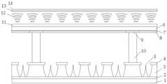
图1是本发明LCD-FED双屏结构高动态显示系统FED结构图。Fig. 1 is a structure diagram of the FED of the LCD-FED dual-screen structure high dynamic display system of the present invention.
图2是本发明LCD-FED双屏结构高动态显示系统一实施例的结构图。Fig. 2 is a structural diagram of an embodiment of the LCD-FED dual-screen structure high dynamic display system of the present invention.
图3是本发明LCD-FED双屏结构高动态显示系统另一实施例的结构图。FIG. 3 is a structural diagram of another embodiment of the LCD-FED dual-screen structure high dynamic display system of the present invention.
图4是本发明LCD-FED双屏结构高动态显示系统再一实施例的结构图。FIG. 4 is a structural diagram of another embodiment of the LCD-FED dual-screen structure high dynamic display system of the present invention.
注:1—FED面板后基板;2—发射电子阴极;3—介质层;4—栅极;5—发射微尖;6—FED面板前基板;7—阳极透明电极;8—荧光粉条;9—黑底;10—支撑体;11—定向层;12—液晶层;13—彩色滤光片;14—LCD液晶面板上基板;15—LCD液晶面板下基板。Note: 1—rear substrate of FED panel; 2—electron emitting cathode; 3—dielectric layer; 4—grid; 5—emission microtip; 6—front substrate of FED panel; 7—anode transparent electrode; - black matrix; 10 - support body; 11 - alignment layer; 12 - liquid crystal layer; 13 - color filter; 14 - upper substrate of LCD liquid crystal panel; 15 - lower substrate of LCD liquid crystal panel.
具体实施方式Detailed ways
为使本发明的目的、技术方案及优点更加清楚明白,以下将通过具体实施例和相关附图,对本发明作进一步详细说明。In order to make the object, technical solution and advantages of the present invention clearer, the present invention will be further described in detail below through specific embodiments and related drawings.
本发明提供一种LCD-FED双屏结构高动态显示系统,包括一LCD液晶面板,其特征在于:还包括一FED面板,设置于所述LCD液晶面板上方作为所述LCD液晶面板的背光源。The present invention provides an LCD-FED dual-screen structure high dynamic display system, which includes an LCD liquid crystal panel, and is characterized in that it also includes an FED panel, which is arranged above the LCD liquid crystal panel as a backlight source for the LCD liquid crystal panel.
如图1所示,在本发明一实施例中所述FED面板包括:As shown in Figure 1, the FED panel described in an embodiment of the present invention includes:
一后基板1;a
一发射电子阴极2,设置于所述后基板1上方;An electron-emitting
一介质层3,设置于所述发射电子阴极2上方并且带有微孔;A
一栅极4,设置于所述介质层3上方并且带有微孔;A
一发射微尖5,设置于所述发射电子阴极2上方并且位于所述介质层3和栅极4的微孔中;An
一前基板6,与所述后基板1相对设置;A
一阳极透明电极7,设置于所述前基板6下方;An anode
一荧光粉条8,设置于所述阳极透明电极7下方并带有间隔;A
一黑底9,设置于所述前基板6下方且位于所述荧光粉条8的间隔中;A
一支撑体10,设置于所述黑底9与所述栅极4之间。A
如图2所示,本实施例提供一种LCD-FED双屏结构高动态显示系统,包括一LCD液晶面板,其特征在于:还包括一FED面板,设置于所述LCD液晶面板上方作为所述LCD液晶面板的背光源。所述FED面板包括:As shown in Figure 2, the present embodiment provides a high dynamic display system with LCD-FED dual-screen structure, which includes an LCD liquid crystal panel, and is characterized in that: it also includes a FED panel, which is arranged above the LCD liquid crystal panel as the The backlight of the LCD liquid crystal panel. The FED panel includes:
一后基板1;a
一发射电子阴极2,设置于所述后基板1上方;An electron-emitting
一介质层3,设置于所述发射电子阴极2上方并且带有微孔;A
一栅极4,设置于所述介质层3上方并且带有微孔;A
一发射微尖5,设置于所述发射电子阴极2上方并且位于所述介质层3和栅极4的微孔中;An
一前基板6,与所述后基板1相对设置;A
一阳极透明电极7,设置于所述前基板6下方;An anode
一荧光粉条8,设置于所述阳极透明电极7下方并带有间隔;A
一黑底9,设置于所述前基板6下方且位于所述荧光粉条8的间隔中;A
一支撑体10,设置于所述黑底9与所述栅极4之间。A
所述LCD液晶面板由两块导电玻璃基片(上基板14和下基板15)夹持着一个液晶层12,封接成一个扁平盒;在所述液晶层12内表面还制作一定向层11,使液晶分子沿两块导电玻璃基片表面都沿面排列,且两块导电玻璃基片表面液晶分子长轴平均方向呈正交排列。还包括一彩色滤光片13,所述彩色滤光片13设置于所述LCD液晶面板的上基板14与液晶层12之间;所述FED面板的前基板6与所述LCD液晶面板的下基板15是同一个基板,减少背光源光线的传播距离。所述FED面板中的一个FED像素点对应所述LCD液晶面板中的一个LCD子像素点,或者所述FED面板中的一个FED像素点对应所述LCD液晶面板中的多个LCD子像素点,或者所述FED面板中的多个FED的像素点对应所述LCD液晶面板中的一个LCD子像素点。所述LCD液晶面板中的液晶为近晶相液晶、向列相液晶或胆甾相液晶,也可为未发现的其他属性的液晶。所述发射微尖为金属微尖、炭纳米管微尖或者石墨烯微尖等一切加电压可发射电子的微尖。The LCD liquid crystal panel is sandwiched by two conductive glass substrates (
所述FED面板结构中的所述阳极透明电极8上只有白色荧光粉条,之间由黑底9隔开,黑底9可以适当减小环境光的反射,提高对比度,同时降低打其他色的可能性。阳极板和阴极板之间有支撑结构,以抵抗大气压。该LCD-FED双屏显示系统,解决了高动态范围显示系统因背光源分辨力低而导致功耗高、局部对比度低、光晕的缺点,而且保持了平板显示轻薄的优点。The anode
如图3所示,本实施例提供一种LCD-FED双屏结构高动态显示系统,包括一LCD液晶面板,其特征在于:还包括一FED面板,设置于所述LCD液晶面板上方作为所述LCD液晶面板的背光源。所述FED面板包括:As shown in Figure 3, the present embodiment provides a high dynamic display system with LCD-FED dual-screen structure, which includes an LCD liquid crystal panel, and is characterized in that: it also includes a FED panel, which is arranged above the LCD liquid crystal panel as the The backlight of the LCD liquid crystal panel. The FED panel includes:
一后基板1;a
一发射电子阴极2,设置于所述后基板1上方;An electron-emitting
一介质层3,设置于所述发射电子阴极2上方并且带有微孔;A
一栅极4,设置于所述介质层3上方并且带有微孔;A
一发射微尖5,设置于所述发射电子阴极2上方并且位于所述介质层3和栅极4的微孔中;An
一前基板6,与所述后基板1相对设置;A
一阳极透明电极7,设置于所述前基板6下方;An anode
一荧光粉条8,设置于所述阳极透明电极7下方并带有间隔;A
一黑底9,设置于所述前基板6下方且位于所述荧光粉条8的间隔中;A
一支撑体10,设置于所述黑底9与所述栅极4之间。A
所述LCD液晶面板由两块导电玻璃基片(上基板14和下基板15)夹持着一个液晶层12,封接成一个扁平盒;在所述液晶层12内表面还制作一定向层11,使液晶分子沿两块导电玻璃基片表面都沿面排列,且两块导电玻璃基片表面液晶分子长轴平均方向呈正交排列。还包括一彩色滤光片13,所述彩色滤光片13设置于所述液晶面板下基板15与所述FED面板前基板6之间;所述FED面板的前基板6是在玻璃上制作,并重叠到所述彩色滤光片13上。所述FED面板中的一个FED像素点对应所述LCD液晶面板中的一个LCD子像素点,或者所述FED面板中的一个FED像素点对应所述LCD液晶面板中的多个LCD子像素点,或者所述FED面板中的多个FED的像素点对应所述LCD液晶面板中的一个LCD子像素点。所述LCD液晶面板中的液晶为近晶相液晶、向列相液晶或胆甾相液晶,也可为未发现的其他属性的液晶。所述发射微尖为金属微尖、炭纳米管微尖或者石墨烯微尖等一切加电压可发射电子的微尖。The LCD liquid crystal panel is sandwiched by two conductive glass substrates (
所述FED面板结构中的所述阳极透明电极8上只有白色荧光粉条,之间由黑底9隔开,黑底9可以适当减小环境光的反射,提高对比度,同时降低打其他色的可能性。阳极板和阴极板之间有支撑结构,以抵抗大气压。该LCD-FED双屏显示系统,解决了高动态范围显示系统因背光源分辨力低而导致功耗高、局部对比度低、光晕的缺点,而且保持了平板显示轻薄的优点。The anode
如图4所示,本实施例提供一种LCD-FED双屏结构高动态显示系统,包括一LCD液晶面板,其特征在于:还包括一FED面板,设置于所述LCD液晶面板上方作为所述LCD液晶面板的背光源。所述FED面板包括:As shown in Figure 4, the present embodiment provides a high dynamic display system with LCD-FED dual-screen structure, which includes an LCD liquid crystal panel, and is characterized in that: it also includes a FED panel, which is arranged above the LCD liquid crystal panel as the The backlight of the LCD liquid crystal panel. The FED panel includes:
一后基板1;a
一发射电子阴极2,设置于所述后基板1上方;An electron-emitting
一介质层3,设置于所述发射电子阴极2上方并且带有微孔;A
一栅极4,设置于所述介质层3上方并且带有微孔;A
一发射微尖5,设置于所述发射电子阴极2上方并且位于所述介质层3和栅极4的微孔中;An
一前基板6,与所述后基板1相对设置;A
一阳极透明电极7,设置于所述前基板6下方;An anode
一荧光粉条8,设置于所述阳极透明电极7下方并带有间隔;A
一黑底9,设置于所述前基板6下方且位于所述荧光粉条8的间隔中;A
一支撑体10,设置于所述黑底9与所述栅极4之间。A
所述LCD液晶面板由两块导电玻璃基片(上基板14和下基板15)夹持着一个液晶层12,封接成一个扁平盒;在所述液晶层12内表面还制作一定向层11,使液晶分子沿两块导电玻璃基片表面都沿面排列,且两块导电玻璃基片表面液晶分子长轴平均方向呈正交排列。所述FED面板的前基板6与所述LCD液晶面板的下基板15是同一个基板,减少背光源光线的传播距离。所述FED面板中的一个FED像素点对应所述LCD液晶面板中的一个LCD子像素点,或者所述FED面板中的一个FED像素点对应所述LCD液晶面板中的多个LCD子像素点,或者所述FED面板中的多个FED的像素点对应所述LCD液晶面板中的一个LCD子像素点。所述LCD液晶面板中的液晶为近晶相液晶、向列相液晶或胆甾相液晶,也可为未发现的其他属性的液晶。所述发射微尖为金属微尖、炭纳米管微尖或者石墨烯微尖等一切加电压可发射电子的微尖。The LCD liquid crystal panel is sandwiched by two conductive glass substrates (
所述FED面板结构中的所述阳极透明电极8上有蓝色荧光粉、红色荧光粉何绿色荧光粉,之间由黑底9隔开,黑底9可以适当减小环境光的反射,提高对比度,同时降低打其他色的可能性。阳极板和阴极板之间有支撑结构,以抵抗大气压。该LCD-FED双屏显示系统,解决了高动态范围显示系统因背光源分辨力低而导致功耗高、局部对比度低、光晕的缺点,而且保持了平板显示轻薄的优点。The anode
在本发明的技术方案中,阴极结构为碳纳米管阴极;栅极结构控制碳纳米管阴极的电子发射;阳极结构中的荧光粉受到阴极电子的轰击发出可见光。利用硅片作为衬底材料制备碳纳米管阴极。采用透明锡铟氧化物(ITO)导电薄膜作为阳极电极的引线,然后在阳极ITO薄膜上印刷荧光粉,在荧光粉与荧光粉之间由黑底隔开。设计与阴极之间由钙钠玻璃作为绝缘隔离支柱。选用低熔点玻璃粉将平板器件的相连处完全密封起来,进行高温固化。最后对显示器件进行排气、封离和拷消。当驱动电路施加电压时,发射微尖发射出电子,由电子轰击荧光粉发光,光线透过阳极透明电极。在本发明LCD-FED双屏结构高动态显示系统结构中,液晶像素点的亮度是由背光源FED控制,其结构中的透明电极在荧光粉的上侧,黑底在透明电极的两侧,因光线为直线传播,当电子轰击荧光粉发光时,扩散到周边像素点的光线被黑底挡住,降低了打其他色的可能性。In the technical solution of the present invention, the cathode structure is a carbon nanotube cathode; the grid structure controls the electron emission of the carbon nanotube cathode; the fluorescent powder in the anode structure is bombarded by cathode electrons to emit visible light. A carbon nanotube cathode was prepared using a silicon wafer as a substrate material. A transparent tin indium oxide (ITO) conductive film is used as the lead wire of the anode electrode, and then phosphor powder is printed on the anode ITO film, and the phosphor powder is separated from the phosphor powder by a black matrix. Soda-lime glass is used as an insulating isolation pillar between the design and the cathode. Use low-melting point glass frit to completely seal the joints of the flat-panel devices and perform high-temperature curing. Finally, exhaust, seal and copy the display device. When the driving circuit applies a voltage, the emitting microtip emits electrons, and the electrons bombard the phosphor to emit light, and the light passes through the anode transparent electrode. In the LCD-FED dual-screen structure high dynamic display system structure of the present invention, the brightness of the liquid crystal pixel is controlled by the backlight source FED, the transparent electrode in the structure is on the upper side of the phosphor, and the black matrix is on both sides of the transparent electrode. Because the light travels in a straight line, when the electrons bombard the phosphor to emit light, the light that diffuses to the surrounding pixels is blocked by the black matrix, reducing the possibility of playing other colors.
本发明还提供一种LCD-FED双屏结构高动态显示系统的显示方法,为实现上述方法,本发明的采用的方案是:The present invention also provides a display method of a LCD-FED dual-screen structure high dynamic display system. In order to realize the above method, the adopted scheme of the present invention is:
一种LCD-FED双屏结构高动态显示系统的显示方法,其特征在于:该系统对输入图像或视频的每一帧图像进行上下面板的分割。提取图像每一像素点的灰度值,存入寄存器矩阵模块中。假设输入图像在(x,y)的值为Lin(x,y,n)(n为像素点(x,y)的通道),Lb(x,y,n)为背光源FED的亮度值,Lf(x,y,n)为液晶面板的亮度值。分割算法如下:A display method for an LCD-FED dual-screen high dynamic display system, characterized in that the system divides each frame of an input image or video into upper and lower panels. The gray value of each pixel of the image is extracted and stored in the register matrix module. Assuming that the value of the input image at (x, y) is Lin (x, y, n) (n is the channel of the pixel (x, y)), Lb (x, y, n) is the brightness value of the backlight FED, Lf (x, y, n) is the brightness value of the liquid crystal panel. The segmentation algorithm is as follows:
Lf(x,y,n)=
Lb(x,y,n)= F(Lin(x,y,n)) (2)Lb(x,y,n) = F(Lin(x,y,n)) (2)
背光源的亮度值由输入图像的亮度值根据非线性函数F(x)求出。由分割算法可知,在液晶面板响应的一帧图像中,把FED分割为256个灰度等级,可得出FED背光式高动态范围显示系统达到256个灰度等级,最大对比度为216:1。当几个FED对应一个LCD像素点时,LCD像素点背光源亮度值为其背光FED亮度值的总和。当一个FED对应一个LCD像素点时,LCD像素点背光源亮度值为其FED亮度值。当一个FED对应几个LCD像素点时,LCD像素点背光源亮度值为在其所对应的LCD点位置图像最大值所求出的FED亮度值。The brightness value of the backlight source is obtained from the brightness value of the input image according to the non-linear function F(x). It can be seen from the segmentation algorithm that in a frame of image responded by the LCD panel, the FED is divided into 256 gray levels, and it can be concluded that the FED backlight high dynamic range display system reaches 256 gray levels, and the maximum contrast ratio is 216:1. When several FEDs correspond to one LCD pixel, the LCD pixel backlight luminance value is the sum of its backlight FED luminance values. When one FED corresponds to one LCD pixel, the LCD pixel backlight luminance value is its FED luminance value. When one FED corresponds to several LCD pixels, the LCD pixel backlight luminance value is the FED luminance value obtained from the maximum value of the image at the corresponding LCD point position.
在本发明的技术方案中,根据所要显示的区域图像内容决定背光源亮度或颜色,并对LCD控制信号进行调制,在保持图像亮度的前提下,有效地节省功耗,提高对比度。在判断到最亮的地方,完全打开该单元格中液晶单元的同时,还给对应的FED单元格加最大的电压,使其亮度达到最大;而最暗的地方则把该单元格中液晶单元完全关闭,同时对应的FED单元格的电压也降低到最小(或者关闭),减轻了漏光现象。采用区域控制的背光源液晶显示算法流程,由输入图像内容决定的背光源驱动信号产生非均匀的动态背光,由输入图像确定LCD的信号。In the technical solution of the present invention, the brightness or color of the backlight source is determined according to the image content of the area to be displayed, and the LCD control signal is modulated to effectively save power consumption and improve contrast while maintaining the brightness of the image. In the brightest place, when the liquid crystal unit in the cell is fully turned on, the maximum voltage is also applied to the corresponding FED cell to make the brightness reach the maximum; and in the darkest place, the liquid crystal unit in the cell is turned on. It is completely closed, and at the same time, the voltage of the corresponding FED cells is also reduced to a minimum (or closed), which reduces the light leakage phenomenon. Using area-controlled backlight liquid crystal display algorithm flow, the backlight driving signal determined by the input image content produces a non-uniform dynamic backlight, and the input image determines the LCD signal.
上列较佳实施例,对本发明的目的、技术方案和优点进行了进一步详细说明,所应理解的是,以上所述仅为本发明的较佳实施例而已,并不用以限制本发明,凡在本发明的精神和原则之内,所作的任何修改、等同替换、改进等,均应包含在本发明的保护范围之内。The above-listed preferred embodiments have further described the purpose, technical solutions and advantages of the present invention in detail. It should be understood that the above descriptions are only preferred embodiments of the present invention, and are not intended to limit the present invention. Within the spirit and principles of the present invention, any modifications, equivalent replacements, improvements, etc., shall be included within the protection scope of the present invention.
Claims (10)
Translated fromChinese
Priority Applications (1)
| Application Number | Priority Date | Filing Date | Title |
|---|---|---|---|
| CN201210435141.7ACN102929039B (en) | 2012-11-05 | 2012-11-05 | Liquid crystal display-field emission display (LCD-FED) double-screen structure high-dynamic display system |
Applications Claiming Priority (1)
| Application Number | Priority Date | Filing Date | Title |
|---|---|---|---|
| CN201210435141.7ACN102929039B (en) | 2012-11-05 | 2012-11-05 | Liquid crystal display-field emission display (LCD-FED) double-screen structure high-dynamic display system |
Publications (2)
| Publication Number | Publication Date |
|---|---|
| CN102929039Atrue CN102929039A (en) | 2013-02-13 |
| CN102929039B CN102929039B (en) | 2015-06-03 |
Family
ID=47643874
Family Applications (1)
| Application Number | Title | Priority Date | Filing Date |
|---|---|---|---|
| CN201210435141.7AExpired - Fee RelatedCN102929039B (en) | 2012-11-05 | 2012-11-05 | Liquid crystal display-field emission display (LCD-FED) double-screen structure high-dynamic display system |
Country Status (1)
| Country | Link |
|---|---|
| CN (1) | CN102929039B (en) |
Cited By (3)
| Publication number | Priority date | Publication date | Assignee | Title |
|---|---|---|---|---|
| CN103747225A (en)* | 2014-01-23 | 2014-04-23 | 福州大学 | High-dynamic-range image dual-screen display method based on color space switching |
| CN104217919A (en)* | 2014-06-06 | 2014-12-17 | 张议聪 | Field emission light-emitting device and method thereof |
| CN104252062A (en)* | 2014-07-04 | 2014-12-31 | 京东方科技集团股份有限公司 | Display substrate, manufacturing method for same and display device |
Citations (5)
| Publication number | Priority date | Publication date | Assignee | Title |
|---|---|---|---|---|
| US5760858A (en)* | 1995-04-21 | 1998-06-02 | Texas Instruments Incorporated | Field emission device panel backlight for liquid crystal displays |
| CN1570728A (en)* | 2004-04-27 | 2005-01-26 | 东南大学 | High-resolution liquid crystal display device with field emission display backlight source |
| CN1855343A (en)* | 2005-04-19 | 2006-11-01 | 财团法人工业技术研究院 | Field emission light source and method of operation thereof |
| CN101479653A (en)* | 2006-06-28 | 2009-07-08 | 汤姆逊许可证公司 | Liquid crystal display having a field emission backlight |
| CN101558351A (en)* | 2006-12-18 | 2009-10-14 | 汤姆森特许公司 | Display device having field emission unit with black matrix |
- 2012
- 2012-11-05CNCN201210435141.7Apatent/CN102929039B/ennot_activeExpired - Fee Related
Patent Citations (5)
| Publication number | Priority date | Publication date | Assignee | Title |
|---|---|---|---|---|
| US5760858A (en)* | 1995-04-21 | 1998-06-02 | Texas Instruments Incorporated | Field emission device panel backlight for liquid crystal displays |
| CN1570728A (en)* | 2004-04-27 | 2005-01-26 | 东南大学 | High-resolution liquid crystal display device with field emission display backlight source |
| CN1855343A (en)* | 2005-04-19 | 2006-11-01 | 财团法人工业技术研究院 | Field emission light source and method of operation thereof |
| CN101479653A (en)* | 2006-06-28 | 2009-07-08 | 汤姆逊许可证公司 | Liquid crystal display having a field emission backlight |
| CN101558351A (en)* | 2006-12-18 | 2009-10-14 | 汤姆森特许公司 | Display device having field emission unit with black matrix |
Cited By (5)
| Publication number | Priority date | Publication date | Assignee | Title |
|---|---|---|---|---|
| CN103747225A (en)* | 2014-01-23 | 2014-04-23 | 福州大学 | High-dynamic-range image dual-screen display method based on color space switching |
| CN103747225B (en)* | 2014-01-23 | 2015-11-18 | 福州大学 | Based on the high dynamic range images double-screen display method of color space conversion |
| CN104217919A (en)* | 2014-06-06 | 2014-12-17 | 张议聪 | Field emission light-emitting device and method thereof |
| CN104252062A (en)* | 2014-07-04 | 2014-12-31 | 京东方科技集团股份有限公司 | Display substrate, manufacturing method for same and display device |
| CN104252062B (en)* | 2014-07-04 | 2017-10-17 | 京东方科技集团股份有限公司 | Display base plate and its manufacture method, display device |
Also Published As
| Publication number | Publication date |
|---|---|
| CN102929039B (en) | 2015-06-03 |
Similar Documents
| Publication | Publication Date | Title |
|---|---|---|
| KR100766925B1 (en) | A light emitting device and a liquid crystal display device using the light emitting device as a back light unit | |
| TW201411250A (en) | Anti-glimpse display apparatus and driving method thereof | |
| CN103715230A (en) | Transparent OLED device and displaying device thereof | |
| WO2020215548A1 (en) | Transparent display panel and transparent display device | |
| CN103715369B (en) | One kind mixing escope and its control method | |
| CN102929039B (en) | Liquid crystal display-field emission display (LCD-FED) double-screen structure high-dynamic display system | |
| US7728494B2 (en) | Light emission device and display device | |
| CN100405524C (en) | Double Sided Field Emission Display | |
| US20090316067A1 (en) | Light emission device and display device using the light emission device as light source | |
| KR100863959B1 (en) | Light emitting device and display device having same | |
| KR20070031756A (en) | Electronic emission display device and driving method thereof | |
| CN101136303A (en) | Light emitting device and display device using same as light source | |
| US8575832B2 (en) | Field emission display | |
| US8552632B2 (en) | Active matrix phosphor cold cathode display | |
| KR100444504B1 (en) | Field emission display | |
| US7671526B2 (en) | Light emission device and display device including the light emission device | |
| CN101183637B (en) | Light emission device and display device using the light emission device as a light source | |
| US8223101B1 (en) | Active matrix phosphor cold cathode display | |
| KR20070031757A (en) | Electron-emitting display device and its driving method | |
| US20200286966A1 (en) | Transparent display panel and displaying method of same | |
| Iguchi et al. | 7.1: Invited Paper: Technologies and Prospects of Fine Pitch Field Emission Display Monitor | |
| CN2904283Y (en) | Flat Panel Display with Tri-Gate Emitter Cathode Control Circuit | |
| KR100830991B1 (en) | Light-emitting device and liquid crystal display device using this light-emitting device as a backlight unit | |
| Yao et al. | The system of High Dynamic Range Display based on the dual structure of the LCD-FED | |
| US20080111460A1 (en) | Light emission device and display device using the light emission device as a light source |
Legal Events
| Date | Code | Title | Description |
|---|---|---|---|
| C06 | Publication | ||
| PB01 | Publication | ||
| C10 | Entry into substantive examination | ||
| SE01 | Entry into force of request for substantive examination | ||
| C14 | Grant of patent or utility model | ||
| GR01 | Patent grant | ||
| CF01 | Termination of patent right due to non-payment of annual fee | ||
| CF01 | Termination of patent right due to non-payment of annual fee | Granted publication date:20150603 Termination date:20191105 |