CN102918650A - Transistor - Google Patents
TransistorDownload PDFInfo
- Publication number
- CN102918650A CN102918650ACN2011800282924ACN201180028292ACN102918650ACN 102918650 ACN102918650 ACN 102918650ACN 2011800282924 ACN2011800282924 ACN 2011800282924ACN 201180028292 ACN201180028292 ACN 201180028292ACN 102918650 ACN102918650 ACN 102918650A
- Authority
- CN
- China
- Prior art keywords
- electrode layer
- layer
- source electrode
- drain electrode
- gate
- Prior art date
- Legal status (The legal status is an assumption and is not a legal conclusion. Google has not performed a legal analysis and makes no representation as to the accuracy of the status listed.)
- Granted
Links
- 239000004065semiconductorSubstances0.000claimsdescription151
- 230000003071parasitic effectEffects0.000abstractdescription43
- 230000007423decreaseEffects0.000abstractdescription7
- 239000010410layerSubstances0.000description487
- 238000010438heat treatmentMethods0.000description35
- 230000015572biosynthetic processEffects0.000description28
- 239000000758substrateSubstances0.000description26
- 239000007789gasSubstances0.000description24
- 238000000034methodMethods0.000description22
- 239000012535impuritySubstances0.000description19
- 239000001257hydrogenSubstances0.000description18
- 229910052739hydrogenInorganic materials0.000description18
- 238000004544sputter depositionMethods0.000description17
- 229910007541Zn OInorganic materials0.000description15
- 239000012298atmosphereSubstances0.000description13
- 229910052760oxygenInorganic materials0.000description13
- XKRFYHLGVUSROY-UHFFFAOYSA-NArgonChemical compound[Ar]XKRFYHLGVUSROY-UHFFFAOYSA-N0.000description12
- QVGXLLKOCUKJST-UHFFFAOYSA-Natomic oxygenChemical compound[O]QVGXLLKOCUKJST-UHFFFAOYSA-N0.000description12
- 239000001301oxygenSubstances0.000description12
- 239000010936titaniumSubstances0.000description11
- XLYOFNOQVPJJNP-UHFFFAOYSA-NwaterSubstancesOXLYOFNOQVPJJNP-UHFFFAOYSA-N0.000description11
- IJGRMHOSHXDMSA-UHFFFAOYSA-NAtomic nitrogenChemical compoundN#NIJGRMHOSHXDMSA-UHFFFAOYSA-N0.000description10
- XUIMIQQOPSSXEZ-UHFFFAOYSA-NSiliconChemical compound[Si]XUIMIQQOPSSXEZ-UHFFFAOYSA-N0.000description10
- 230000008569processEffects0.000description10
- 229910052710siliconInorganic materials0.000description10
- 239000010703siliconSubstances0.000description10
- UFHFLCQGNIYNRP-UHFFFAOYSA-NHydrogenChemical compound[H][H]UFHFLCQGNIYNRP-UHFFFAOYSA-N0.000description9
- 230000001681protective effectEffects0.000description9
- VYPSYNLAJGMNEJ-UHFFFAOYSA-NSilicium dioxideChemical compoundO=[Si]=OVYPSYNLAJGMNEJ-UHFFFAOYSA-N0.000description8
- 150000002431hydrogenChemical class0.000description8
- 229910052814silicon oxideInorganic materials0.000description8
- 229910052581Si3N4Inorganic materials0.000description7
- 238000010586diagramMethods0.000description7
- HQVNEWCFYHHQES-UHFFFAOYSA-Nsilicon nitrideChemical compoundN12[Si]34N5[Si]62N3[Si]51N64HQVNEWCFYHHQES-UHFFFAOYSA-N0.000description7
- 229910052719titaniumInorganic materials0.000description7
- 229910052782aluminiumInorganic materials0.000description6
- 229910052786argonInorganic materials0.000description6
- 238000004519manufacturing processMethods0.000description6
- 229910052757nitrogenInorganic materials0.000description6
- 238000000206photolithographyMethods0.000description6
- 229910052721tungstenInorganic materials0.000description6
- MYMOFIZGZYHOMD-UHFFFAOYSA-NDioxygenChemical compoundO=OMYMOFIZGZYHOMD-UHFFFAOYSA-N0.000description5
- RTAQQCXQSZGOHL-UHFFFAOYSA-NTitaniumChemical compound[Ti]RTAQQCXQSZGOHL-UHFFFAOYSA-N0.000description5
- XAGFODPZIPBFFR-UHFFFAOYSA-NaluminiumChemical compound[Al]XAGFODPZIPBFFR-UHFFFAOYSA-N0.000description5
- 239000013078crystalSubstances0.000description5
- 229910001882dioxygenInorganic materials0.000description5
- 125000002887hydroxy groupChemical group[H]O*0.000description5
- 229910044991metal oxideInorganic materials0.000description5
- 150000004706metal oxidesChemical group0.000description5
- 238000005530etchingMethods0.000description4
- 150000004678hydridesChemical class0.000description4
- 239000011261inert gasSubstances0.000description4
- 238000005259measurementMethods0.000description4
- 229910052751metalInorganic materials0.000description4
- 239000002184metalSubstances0.000description4
- 239000000203mixtureSubstances0.000description4
- 230000009467reductionEffects0.000description4
- 239000010937tungstenSubstances0.000description4
- QTBSBXVTEAMEQO-UHFFFAOYSA-NAcetic acidChemical compoundCC(O)=OQTBSBXVTEAMEQO-UHFFFAOYSA-N0.000description3
- 229910019092Mg-OInorganic materials0.000description3
- 229910019395Mg—OInorganic materials0.000description3
- MWUXSHHQAYIFBG-UHFFFAOYSA-NNitric oxideChemical compoundO=[N]MWUXSHHQAYIFBG-UHFFFAOYSA-N0.000description3
- 229910052734heliumInorganic materials0.000description3
- 239000001307heliumSubstances0.000description3
- SWQJXJOGLNCZEY-UHFFFAOYSA-Nhelium atomChemical compound[He]SWQJXJOGLNCZEY-UHFFFAOYSA-N0.000description3
- 239000000463materialSubstances0.000description3
- 229910052750molybdenumInorganic materials0.000description3
- 150000004767nitridesChemical class0.000description3
- 238000005268plasma chemical vapour depositionMethods0.000description3
- 238000012545processingMethods0.000description3
- 238000001552radio frequency sputter depositionMethods0.000description3
- -1tungsten nitrideChemical class0.000description3
- 229910005191Ga 2 O 3Inorganic materials0.000description2
- GQPLMRYTRLFLPF-UHFFFAOYSA-NNitrous OxideChemical compound[O-][N+]#NGQPLMRYTRLFLPF-UHFFFAOYSA-N0.000description2
- NBIIXXVUZAFLBC-UHFFFAOYSA-NPhosphoric acidChemical compoundOP(O)(O)=ONBIIXXVUZAFLBC-UHFFFAOYSA-N0.000description2
- NRTOMJZYCJJWKI-UHFFFAOYSA-NTitanium nitrideChemical compound[Ti]#NNRTOMJZYCJJWKI-UHFFFAOYSA-N0.000description2
- 239000012300argon atmosphereSubstances0.000description2
- 230000008859changeEffects0.000description2
- 150000001875compoundsChemical class0.000description2
- 229910052802copperInorganic materials0.000description2
- 239000010949copperSubstances0.000description2
- PMHQVHHXPFUNSP-UHFFFAOYSA-Mcopper(1+);methylsulfanylmethane;bromideChemical compoundBr[Cu].CSCPMHQVHHXPFUNSP-UHFFFAOYSA-M0.000description2
- 230000007547defectEffects0.000description2
- 238000011161developmentMethods0.000description2
- 239000000428dustSubstances0.000description2
- 238000011049fillingMethods0.000description2
- 229910052733galliumInorganic materials0.000description2
- 239000011521glassSubstances0.000description2
- 125000004435hydrogen atomChemical group[H]*0.000description2
- 229910052738indiumInorganic materials0.000description2
- 239000004973liquid crystal related substanceSubstances0.000description2
- 239000007769metal materialSubstances0.000description2
- 229910052754neonInorganic materials0.000description2
- GKAOGPIIYCISHV-UHFFFAOYSA-Nneon atomChemical compound[Ne]GKAOGPIIYCISHV-UHFFFAOYSA-N0.000description2
- 239000012299nitrogen atmosphereSubstances0.000description2
- TWNQGVIAIRXVLR-UHFFFAOYSA-Noxo(oxoalumanyloxy)alumaneChemical compoundO=[Al]O[Al]=OTWNQGVIAIRXVLR-UHFFFAOYSA-N0.000description2
- 238000009832plasma treatmentMethods0.000description2
- 230000005855radiationEffects0.000description2
- 239000000523sampleSubstances0.000description2
- 239000002356single layerSubstances0.000description2
- 239000000126substanceSubstances0.000description2
- 229910052715tantalumInorganic materials0.000description2
- WFKWXMTUELFFGS-UHFFFAOYSA-NtungstenChemical compound[W]WFKWXMTUELFFGS-UHFFFAOYSA-N0.000description2
- 238000001039wet etchingMethods0.000description2
- VHUUQVKOLVNVRT-UHFFFAOYSA-NAmmonium hydroxideChemical compound[NH4+].[OH-]VHUUQVKOLVNVRT-UHFFFAOYSA-N0.000description1
- OKTJSMMVPCPJKN-UHFFFAOYSA-NCarbonChemical compound[C]OKTJSMMVPCPJKN-UHFFFAOYSA-N0.000description1
- RYGMFSIKBFXOCR-UHFFFAOYSA-NCopperChemical compound[Cu]RYGMFSIKBFXOCR-UHFFFAOYSA-N0.000description1
- GYHNNYVSQQEPJS-UHFFFAOYSA-NGalliumChemical compound[Ga]GYHNNYVSQQEPJS-UHFFFAOYSA-N0.000description1
- 244000126211Hericium coralloidesSpecies0.000description1
- MHAJPDPJQMAIIY-UHFFFAOYSA-NHydrogen peroxideChemical compoundOOMHAJPDPJQMAIIY-UHFFFAOYSA-N0.000description1
- DGAQECJNVWCQMB-PUAWFVPOSA-MIlexoside XXIXChemical compoundC[C@@H]1CC[C@@]2(CC[C@@]3(C(=CC[C@H]4[C@]3(CC[C@@H]5[C@@]4(CC[C@@H](C5(C)C)OS(=O)(=O)[O-])C)C)[C@@H]2[C@]1(C)O)C)C(=O)O[C@H]6[C@@H]([C@H]([C@@H]([C@H](O6)CO)O)O)O.[Na+]DGAQECJNVWCQMB-PUAWFVPOSA-M0.000description1
- 108010083687Ion PumpsProteins0.000description1
- ZOKXTWBITQBERF-UHFFFAOYSA-NMolybdenumChemical compound[Mo]ZOKXTWBITQBERF-UHFFFAOYSA-N0.000description1
- 229910052779NeodymiumInorganic materials0.000description1
- GRYLNZFGIOXLOG-UHFFFAOYSA-NNitric acidChemical compoundO[N+]([O-])=OGRYLNZFGIOXLOG-UHFFFAOYSA-N0.000description1
- 229910004298SiO 2Inorganic materials0.000description1
- 229910020923Sn-OInorganic materials0.000description1
- 230000009471actionEffects0.000description1
- 239000000956alloySubstances0.000description1
- 229910000147aluminium phosphateInorganic materials0.000description1
- 235000011114ammonium hydroxideNutrition0.000description1
- SWXQKHHHCFXQJF-UHFFFAOYSA-Nazane;hydrogen peroxideChemical compound[NH4+].[O-]OSWXQKHHHCFXQJF-UHFFFAOYSA-N0.000description1
- GPBUGPUPKAGMDK-UHFFFAOYSA-NazanylidynemolybdenumChemical compound[Mo]#NGPBUGPUPKAGMDK-UHFFFAOYSA-N0.000description1
- 230000004888barrier functionEffects0.000description1
- 229910052799carbonInorganic materials0.000description1
- 125000004432carbon atomChemical groupC*0.000description1
- 229910052804chromiumInorganic materials0.000description1
- 230000018044dehydrationEffects0.000description1
- 238000006297dehydration reactionMethods0.000description1
- 238000006356dehydrogenation reactionMethods0.000description1
- 238000001312dry etchingMethods0.000description1
- 230000005684electric fieldEffects0.000description1
- 238000000605extractionMethods0.000description1
- 230000005669field effectEffects0.000description1
- 239000010419fine particleSubstances0.000description1
- 229910000449hafnium oxideInorganic materials0.000description1
- WIHZLLGSGQNAGK-UHFFFAOYSA-Nhafnium(4+);oxygen(2-)Chemical compound[O-2].[O-2].[Hf+4]WIHZLLGSGQNAGK-UHFFFAOYSA-N0.000description1
- 229910052736halogenInorganic materials0.000description1
- 150000002367halogensChemical class0.000description1
- 150000002483hydrogen compoundsChemical class0.000description1
- APFVFJFRJDLVQX-UHFFFAOYSA-Nindium atomChemical compound[In]APFVFJFRJDLVQX-UHFFFAOYSA-N0.000description1
- 238000010030laminatingMethods0.000description1
- QSHDDOUJBYECFT-UHFFFAOYSA-NmercuryChemical compound[Hg]QSHDDOUJBYECFT-UHFFFAOYSA-N0.000description1
- 229910052753mercuryInorganic materials0.000description1
- 229910001507metal halideInorganic materials0.000description1
- 150000005309metal halidesChemical class0.000description1
- 239000011259mixed solutionSubstances0.000description1
- 230000004048modificationEffects0.000description1
- 238000012986modificationMethods0.000description1
- 239000011733molybdenumSubstances0.000description1
- 229910000476molybdenum oxideInorganic materials0.000description1
- QEFYFXOXNSNQGX-UHFFFAOYSA-Nneodymium atomChemical compound[Nd]QEFYFXOXNSNQGX-UHFFFAOYSA-N0.000description1
- 229910017604nitric acidInorganic materials0.000description1
- PQQKPALAQIIWST-UHFFFAOYSA-NoxomolybdenumChemical compound[Mo]=OPQQKPALAQIIWST-UHFFFAOYSA-N0.000description1
- 239000002245particleSubstances0.000description1
- 238000002294plasma sputter depositionMethods0.000description1
- 238000000746purificationMethods0.000description1
- 239000003870refractory metalSubstances0.000description1
- 238000012827research and developmentMethods0.000description1
- 229910052706scandiumInorganic materials0.000description1
- SIXSYDAISGFNSX-UHFFFAOYSA-Nscandium atomChemical compound[Sc]SIXSYDAISGFNSX-UHFFFAOYSA-N0.000description1
- 229910052708sodiumInorganic materials0.000description1
- 239000011734sodiumSubstances0.000description1
- 239000000243solutionSubstances0.000description1
- 238000000859sublimationMethods0.000description1
- 230000008022sublimationEffects0.000description1
- GUVRBAGPIYLISA-UHFFFAOYSA-Ntantalum atomChemical compound[Ta]GUVRBAGPIYLISA-UHFFFAOYSA-N0.000description1
- JBQYATWDVHIOAR-UHFFFAOYSA-NtellanylidenegermaniumChemical compound[Te]=[Ge]JBQYATWDVHIOAR-UHFFFAOYSA-N0.000description1
- 238000012546transferMethods0.000description1
- 229910052724xenonInorganic materials0.000description1
- FHNFHKCVQCLJFQ-UHFFFAOYSA-Nxenon atomChemical compound[Xe]FHNFHKCVQCLJFQ-UHFFFAOYSA-N0.000description1
- 229910052725zincInorganic materials0.000description1
- 239000011701zincSubstances0.000description1
Images


Classifications
- H—ELECTRICITY
- H10—SEMICONDUCTOR DEVICES; ELECTRIC SOLID-STATE DEVICES NOT OTHERWISE PROVIDED FOR
- H10D—INORGANIC ELECTRIC SEMICONDUCTOR DEVICES
- H10D30/00—Field-effect transistors [FET]
- H10D30/60—Insulated-gate field-effect transistors [IGFET]
- H10D30/67—Thin-film transistors [TFT]
- H10D30/6729—Thin-film transistors [TFT] characterised by the electrodes
- H—ELECTRICITY
- H10—SEMICONDUCTOR DEVICES; ELECTRIC SOLID-STATE DEVICES NOT OTHERWISE PROVIDED FOR
- H10D—INORGANIC ELECTRIC SEMICONDUCTOR DEVICES
- H10D30/00—Field-effect transistors [FET]
- H10D30/60—Insulated-gate field-effect transistors [IGFET]
- H10D30/67—Thin-film transistors [TFT]
- H10D30/6704—Thin-film transistors [TFT] having supplementary regions or layers in the thin films or in the insulated bulk substrates for controlling properties of the device
- H—ELECTRICITY
- H10—SEMICONDUCTOR DEVICES; ELECTRIC SOLID-STATE DEVICES NOT OTHERWISE PROVIDED FOR
- H10D—INORGANIC ELECTRIC SEMICONDUCTOR DEVICES
- H10D30/00—Field-effect transistors [FET]
- H10D30/60—Insulated-gate field-effect transistors [IGFET]
- H10D30/67—Thin-film transistors [TFT]
- H10D30/674—Thin-film transistors [TFT] characterised by the active materials
- H10D30/6755—Oxide semiconductors, e.g. zinc oxide, copper aluminium oxide or cadmium stannate
Landscapes
- Thin Film Transistor (AREA)
- Electrodes Of Semiconductors (AREA)
Abstract
Description
Translated fromChinese技术领域technical field
本发明涉及一种晶体管,并且本发明的一个示例涉及一种晶体管的电极形状。The present invention relates to a transistor, and an example of the present invention relates to an electrode shape of a transistor.
背景技术Background technique
随着信息化的进展,代替纸的薄而轻的电子纸显示器和可瞬时识别每个商品的IC标签等的开发受到关注。此外,液晶显示装置从电视接收机等大型显示装置到移动电话机等小型显示装置得到广泛使用。随着这些装置的普及,开展了以低成本化或高增值化为目的的研究开发。特别近年来,人们对地球环境的关注不断增强,因此能够实现低耗电工作和高速工作的装置的开发受到关注。With the advancement of informatization, the development of thin and light electronic paper displays that replace paper and IC tags that can instantly identify each product has attracted attention. In addition, liquid crystal display devices are widely used from large display devices such as television receivers to small display devices such as mobile phones. Along with the widespread use of these devices, research and development for the purpose of cost reduction or high added value has been carried out. Especially in recent years, people's attention to the global environment has been increasing, and therefore, the development of devices capable of low power consumption operation and high-speed operation has attracted attention.
现阶段,在这些装置中,晶体管作为元件被使用。晶体管是这样的元件:通过在半导体中设置称作源区和漏区的区域并连接到相应的电极,对该电极施加电位,通过绝缘层或肖特基势垒借助于称作栅极的电极对半导体施加电场来控制半导体的状态,由此控制在源电极和漏电极之间流过的电流。At present, in these devices, transistors are used as elements. Transistors are elements that, by providing regions called source and drain regions in a semiconductor and connecting them to corresponding electrodes, to which an electric potential is applied, through an insulating layer or a Schottky barrier by means of an electrode called a gate Applying an electric field to the semiconductor controls the state of the semiconductor, thereby controlling the current flowing between the source and drain electrodes.
为了制造能够实现低耗电工作和高速工作的装置,需要具有更大的导通/截止比以及更小的寄生电容的晶体管。导通/截止比是通态电流和断态电流的比率(ION/IOFF),该导通/截止比越大,开关特性越好。另外,通态电流是当晶体管处于导通时在源电极和漏电极之间流过的电流,断态电流是当晶体管处于截止状态时在源电极和漏电极之间流过的电流。例如,在n沟道晶体管中,断态电流是当栅极电压低于晶体管的阈值电压时在源电极和漏电极之间流过的电流。寄生电容是在源电极(漏电极)与栅电极的重叠部分产生的电容,并且寄生电容越大,越造成开关时间的增加和对交流信号的传递增益的下降。In order to manufacture devices capable of low power consumption operation and high-speed operation, transistors having a larger on/off ratio and smaller parasitic capacitance are required. The on/off ratio is the ratio of the on-state current to the off-state current (ION /IOFF ), and the larger the on/off ratio, the better the switching characteristics. In addition, the on-state current is the current flowing between the source electrode and the drain electrode when the transistor is on, and the off-state current is the current flowing between the source electrode and the drain electrode when the transistor is in the off state. For example, in an n-channel transistor, the off-state current is the current that flows between the source and drain electrodes when the gate voltage is lower than the threshold voltage of the transistor. Parasitic capacitance is the capacitance generated at the overlapping portion of the source electrode (drain electrode) and the gate electrode, and the larger the parasitic capacitance, the more the switching time will increase and the transfer gain of the AC signal will decrease.
晶体管的寄生电容依赖于源电极(漏电极)与栅电极的重叠部分的面积而发生变化。通过减少该面积,可以降低寄生电容。然而,该面积的减少和制造成本之间存在着权衡关系,并且均衡它们是非常难的。The parasitic capacitance of a transistor changes depending on the area of the overlapping portion of the source electrode (drain electrode) and the gate electrode. By reducing this area, parasitic capacitance can be reduced. However, there is a trade-off between this area reduction and manufacturing cost, and balancing them is very difficult.
晶体管的通态电流依赖于沟道形成区的长度和宽度而发生变化。沟道形成区的长度相当于彼此相对的源电极的边缘和漏电极的边缘之间的长度。通过减少该长度,可以增大通态电流。沟道形成区的宽度相当于源电极和漏电极彼此相对的长度。通过增大该宽度,可以增大通态电流。例如,已公开了如下结构的晶体管:通过将晶体管的源电极和漏电极都形成为具有梳形而且使其彼此交错设置,使晶体管的沟道形成区的宽度增大,而允许源电极(漏电极)与栅电极的未对准(例如,参照专利文献1)。然而,在该结构中,源电极(漏电极)与栅电极重叠的面积较大,而使寄生电容增大。若为了降低寄生电容而减少源电极(漏电极)与栅电极重叠的面积,则通态电流下降。The on-state current of the transistor varies depending on the length and width of the channel formation region. The length of the channel formation region corresponds to the length between the edge of the source electrode and the edge of the drain electrode facing each other. By reducing this length, the on-state current can be increased. The width of the channel formation region corresponds to the length of the source electrode and the drain electrode facing each other. By increasing this width, on-state current can be increased. For example, there has been disclosed a transistor having a structure in which the width of the channel formation region of the transistor is increased by forming both the source electrode and the drain electrode of the transistor to have a comb shape and interlaced with each other, allowing the source (drain) electrode) and gate electrode misalignment (for example, refer to Patent Document 1). However, in this structure, the overlapping area of the source electrode (drain electrode) and the gate electrode is large, increasing the parasitic capacitance. If the overlapping area of the source electrode (drain electrode) and the gate electrode is reduced in order to reduce the parasitic capacitance, the on-state current decreases.
再者,当将沟道形成区的长度过度增大时,会引起通态电流急剧下降的问题。为了保持一定值以上的通态电流,需要将沟道形成区的长度(当将栅极宽度固定时,也可以为源(漏)电极与栅电极的重叠部分的长度)保持为一定值以下。也就是说,需要一种可以不改变沟道形成区的长度(当将栅极宽度固定时,不改变源(漏)电极与栅电极的重叠部分的长度)地减少重叠部分的面积的晶体管。Furthermore, when the length of the channel formation region is excessively increased, a problem of a sharp drop in on-state current arises. In order to keep the on-state current above a certain value, it is necessary to keep the length of the channel formation region (when the gate width is fixed, the length of the overlapping portion of the source (drain) electrode and the gate electrode) below a certain value. That is, there is a need for a transistor capable of reducing the area of the overlapping portion without changing the length of the channel formation region (when the gate width is fixed, without changing the length of the overlapping portion between the source (drain) electrode and the gate electrode).
[专利文献1] 日本专利申请特开昭62-287666号公报。[Patent Document 1] Japanese Patent Application Laid-Open No. 62-287666.
发明内容Contents of the invention
鉴于上述问题,本发明的一个示例的目的是在降低在源电极(漏电极)与栅电极的重叠部分产生的寄生电容的同时,抑制通态电流的下降。In view of the above problems, an object of one example of the present invention is to suppress a drop in on-state current while reducing parasitic capacitance generated at an overlapping portion of a source electrode (drain electrode) and a gate electrode.
通过将晶体管的源电极层和漏电极层形成为梳形,来达到上述目的。The above object is achieved by forming the source electrode layer and the drain electrode layer of the transistor into a comb shape.
本发明的一个示例是一种晶体管,包括:形成为梳形的源电极层,该源电极层包括以预定间隔隔开的相邻设置的电极齿形部分和用于连接该电极齿形部分的连接部分;以及形成为梳形的漏电极层,该漏电极层包括以预定间隔隔开的相邻设置的电极齿形部分和用于连接该电极齿形部分的连接部分,其中,源电极层和漏电极层设置为使得源电极层的电极齿形部分与漏电极层的电极齿形部分彼此相对但不彼此交错。源电极层的电极齿形部分中的一个的端部和漏电极层的电极齿形部分中的一个的端部彼此相对。下面,将该结构称作结构A。源电极层的电极齿形部分的端部和漏电极层的电极齿形部分的端部可以沿相同长度彼此相对。An example of the present invention is a transistor including: a source electrode layer formed in a comb shape, the source electrode layer including adjacently arranged electrode tooth-shaped portions spaced apart at predetermined intervals and an electrode for connecting the electrode tooth-shaped portions a connecting portion; and a comb-shaped drain electrode layer comprising adjacently disposed electrode tooth-shaped portions spaced apart at predetermined intervals and a connecting portion for connecting the electrode tooth-shaped portions, wherein the source electrode layer The and drain electrode layers are arranged such that the electrode serrations of the source electrode layer and the electrode serrations of the drain electrode layer face each other but do not cross each other. An end portion of one of the electrode tooth portions of the source electrode layer and an end portion of one of the electrode tooth portions of the drain electrode layer are opposed to each other. Hereinafter, this structure is referred to as structure A. An end portion of the electrode tooth portion of the source electrode layer and an end portion of the electrode tooth portion of the drain electrode layer may be opposed to each other along the same length.
本发明的一个示例是一种晶体管,包括:形成为梳形的源电极层,该源电极层包括以预定间隔隔开的相邻设置的电极齿形部分和用于连接该电极齿形部分的连接部分;以及形成为梳形的漏电极层,该漏电极层包括以预定间隔隔开的相邻设置的电极齿形部分和用于连接该电极齿形部分的连接部分,其中,源电极层和漏电极层设置为源电极层的电极齿形部分和漏电极层的电极齿形部分彼此相对但不彼此交错,并且源电极层的电极齿形部分中的一个的端部和漏电极层的电极齿形部分中的一个的端部沿与源电极层的电极齿形部分的端部的长度或漏电极层的电极齿形部分的端部的长度不同的长度彼此相对(不对准)。下面,将该结构称作结构B。An example of the present invention is a transistor including: a source electrode layer formed in a comb shape, the source electrode layer including adjacently arranged electrode tooth-shaped portions spaced apart at predetermined intervals and an electrode for connecting the electrode tooth-shaped portions a connecting portion; and a comb-shaped drain electrode layer comprising adjacently disposed electrode tooth-shaped portions spaced apart at predetermined intervals and a connecting portion for connecting the electrode tooth-shaped portions, wherein the source electrode layer and the drain electrode layer are arranged such that the electrode tooth-shaped portion of the source electrode layer and the electrode tooth-shaped portion of the drain electrode layer face each other but do not cross each other, and the end of one of the electrode tooth-shaped portions of the source electrode layer and the drain electrode layer Ends of one of the electrode toothed portions are opposed to (misaligned with) each other along a length different from the length of the end of the electrode toothed portion of the source electrode layer or the length of the end of the electrode toothed portion of the drain electrode layer. Hereinafter, this structure is referred to as structure B.
本发明的一个示例是一种晶体管,包括:形成为梳形的源电极层,该源电极层包括以预定间隔隔开的相邻设置的电极齿形部分和用于连接该电极齿形部分的连接部分;以及形成为矩形的漏电极层,其中,漏电极层和源电极层设置为使得漏电极层和源电极层的电极齿形部分彼此相对。下面,将该结构称作结构C。An example of the present invention is a transistor including: a source electrode layer formed in a comb shape, the source electrode layer including adjacently arranged electrode tooth-shaped portions spaced apart at predetermined intervals and an electrode for connecting the electrode tooth-shaped portions a connection portion; and a drain electrode layer formed in a rectangular shape, wherein the drain electrode layer and the source electrode layer are arranged such that electrode tooth-shaped portions of the drain electrode layer and the source electrode layer face each other. Hereinafter, this structure is referred to as structure C.
本发明的一个示例是一种晶体管,包括:形成为梳形的漏电极层,该漏电极层包括以预定间隔隔开的相邻设置的电极齿形部分和用于连接该电极齿形部分的连接部分;以及形成为矩形的源电极层,其中,源电极层和漏电极层设置为使得源电极层和漏电极层的电极齿形部分彼此相对。下面,将该结构称作结构C。An example of the present invention is a transistor including: a drain electrode layer formed in a comb shape, the drain electrode layer including adjacently arranged electrode tooth-shaped portions spaced apart at predetermined intervals; a connection portion; and a source electrode layer formed in a rectangular shape, wherein the source electrode layer and the drain electrode layer are arranged such that electrode tooth-shaped portions of the source electrode layer and the drain electrode layer face each other. Hereinafter, this structure is referred to as structure C.
以上的任意晶体管可包括:栅电极层;与栅电极层接触的栅极绝缘层;隔着栅极绝缘层与栅电极层重叠的半导体层。源电极层的边缘可与半导体层的一侧接触并且可隔着栅极绝缘层及半导体层与栅电极层重叠;漏电极层的边缘与半导体层的一侧接触并且可隔着栅极绝缘层及半导体层与栅电极层重叠。Any of the above transistors may include: a gate electrode layer; a gate insulating layer in contact with the gate electrode layer; and a semiconductor layer overlapping the gate electrode layer via the gate insulating layer. The edge of the source electrode layer can be in contact with one side of the semiconductor layer and can overlap the gate electrode layer through the gate insulating layer and the semiconductor layer; the edge of the drain electrode layer can be in contact with one side of the semiconductor layer and can be separated from the gate insulating layer And the semiconductor layer overlaps with the gate electrode layer.
在以上的一些晶体管中,源电极层(梳形电极层)的连接部分与栅电极层彼此不重叠,并且漏电极层(梳形电极层)的连接部分与栅电极层彼此不重叠。In some of the above transistors, the connection portion of the source electrode layer (comb-shaped electrode layer) and the gate electrode layer do not overlap each other, and the connection portion of the drain electrode layer (comb-shaped electrode layer) and the gate electrode layer do not overlap each other.
在以上的一些晶体管中,梳形源电极层的端部的宽度可为源电极层的宽度的3/8以上且1/1以下,并且是漏电极层的宽度的3/8以上且8/3以下。In some of the above transistors, the width of the end portion of the comb-shaped source electrode layer may be 3/8 or more and 1/1 or less of the width of the source electrode layer, and be 3/8 or more and 8/3 of the width of the drain electrode layer. 3 or less.
在以上的一些晶体管中,梳形漏电极层的端部的宽度可为漏电极层的宽度的3/8以上且1/1以下,并且是源电极层的宽度的3/8以上且8/3以下。In some of the above transistors, the width of the end of the comb-shaped drain electrode layer may be 3/8 or more and 1/1 or less of the width of the drain electrode layer, and be 3/8 or more and 8/3 or more of the width of the source electrode layer. 3 or less.
在以上的任意晶体管中,各电极齿形部分之间的间隔可大于0μm且为5μm以下。In any of the above transistors, the interval between the respective electrode serrations may be greater than 0 μm and 5 μm or less.
另外,当该晶体管不满足上述条件时,通态电流的下降可超过允许范围。然而,在本说明书中,通态电流降低几%左右可以认为能够保持通态电流。In addition, when the transistor does not meet the above conditions, the drop in on-state current may exceed the allowable range. However, in this specification, it can be considered that the on-state current can be maintained by reducing the on-state current by about several percent.
在下文中,简单说明本说明书中使用的术语。在本说明书中,术语“梳形”是指具有凹部和凸部的任意形状。术语“梳形电极层”是指其边缘具有凹部和凸部的源(漏)电极层整体,术语“梳形电极层(源电极层或漏电极层)的端部(也称为端头)”是指除连接部分的边缘以外的平行于连接部分的边缘且与栅电极层重叠的源(漏)电极层的各电极齿形部分的所有端部,术语“梳形电极层的端部的宽度”是指除连接部分的边缘以外的平行于连接部分的边缘且与栅电极层重叠的源(漏)电极层的电极齿形部分的所有端部的长度总和。术语“电极齿形部分之间的间隔”是指从栅电极层的边缘与重叠于栅电极层的源(漏)电极层的电极齿形部分的交点到栅电极层的边缘与重叠于栅电极层的源(漏)电极层的下一个电极齿形部分的交点的、栅电极层与源(漏)电极层彼此不重叠的区域中的栅电极层的边缘的长度。Hereinafter, terms used in this specification are briefly explained. In this specification, the term "comb-shaped" means an arbitrary shape having concavities and convexities. The term "comb-shaped electrode layer" refers to the whole of the source (drain) electrode layer with concave and convex parts on its edge, and the term "comb-shaped electrode layer (source electrode layer or drain electrode layer) ends (also called terminals) "Refers to all ends of each electrode tooth-shaped part of the source (drain) electrode layer that is parallel to the edge of the connection part and overlaps with the gate electrode layer, except for the edge of the connection part. The term "the end of the comb-shaped electrode layer "Width" refers to the sum of the lengths of all ends of the electrode tooth-shaped portion of the source (drain) electrode layer parallel to the edge of the connection portion and overlapping with the gate electrode layer except for the edge of the connection portion. The term "interval between the electrode serrations" means from the intersection of the edge of the gate electrode layer and the electrode serration of the source (drain) electrode layer overlapping the gate electrode layer to the edge of the gate electrode layer and the overlap of the gate electrode The length of the edge of the gate electrode layer in the area where the gate electrode layer and the source (drain) electrode layer do not overlap each other at the intersection of the next electrode tooth-shaped portion of the source (drain) electrode layer of the layer.
在本说明书中,“源”和“漏”的功能例如当采用相反极性的晶体管时或电流方向在电路工作中发生变化时有时可彼此互换。因此,在本说明书中,可以将术语“源”和“漏”互相替换地使用以标记漏和源。In this specification, the functions of "source" and "drain" are sometimes interchanged with each other, for example when using transistors of opposite polarity or when the direction of current flow is changed during circuit operation. Therefore, in this specification, the terms "source" and "drain" may be used interchangeably to denote drain and source.
另外,本说明书中使用的表示程度的术语如“大致”、“大约”、“稍微”、“左右”等意味着从被修饰的术语的合理偏离而使得最终结果不明显地发生变化,除非该偏离将否定它所修饰的术语的含义。In addition, terms of degree such as "approximately", "approximately", "slightly", "around" and the like used in this specification mean a reasonable deviation from the modified term such that the end result does not change significantly, unless the A deviation would negate the meaning of the term it modifies.
通过将半导体层上延伸的源电极(漏电极)层形成为梳形,可以减少源电极(漏电极)层与栅电极层彼此重叠的部分的面积,从而可以降低寄生电容。再者,通过将梳形的源电极层和漏电极层设置为其梳齿部分彼此相对,可以利用间接电流,从而可以提供通态电流不下降的晶体管。By forming the source electrode (drain electrode) layer extending over the semiconductor layer into a comb shape, the area of the portion where the source electrode (drain electrode) layer and the gate electrode layer overlap each other can be reduced, thereby reducing parasitic capacitance. Furthermore, by arranging the comb-shaped source electrode layer and drain electrode layer such that the comb-tooth portions thereof face each other, indirect current can be utilized, whereby a transistor in which on-state current does not drop can be provided.
附图说明Description of drawings
图1A和1B是说明实施例1的晶体管的图;1A and 1B are diagrams illustrating a transistor of
图2A和2B是说明实施例1的晶体管的图;2A and 2B are diagrams illustrating transistors of
图3A和3B是说明实施例1的晶体管的图;3A and 3B are diagrams illustrating transistors of
图4A和4B是说明实施例1的晶体管的电流通路的图;4A and 4B are diagrams illustrating current paths of transistors of
图5A和5B是说明示例1的晶体管的图;5A and 5B are diagrams illustrating transistors of Example 1;
图6A和6B是说明示例1的晶体管的图;6A and 6B are diagrams illustrating transistors of Example 1;
图7A至7D是示出示例1的晶体管的电容特性的图;7A to 7D are graphs showing capacitance characteristics of transistors of Example 1;
图8A和8B是示出示例1的晶体管的电流特性的图;8A and 8B are graphs showing current characteristics of transistors of Example 1;
图9A至9E是说明实施例2的晶体管的图。9A to 9E are diagrams illustrating transistors of
具体实施方式Detailed ways
将参照附图详细说明实施例。但是,本发明不局限于下面的说明,所属技术领域的普通技术人员可以很容易地意识到,本发明的方式和详细内容在不脱离本发明的思想及其范围下可以被变换为各种形式。因此,本发明不应该被解释为限定于下面的实施例的描述。另外,在不同附图中,使用相同的参考标号来表示相同部分或具有类似功能的部分,而省略其重复说明。Embodiments will be described in detail with reference to the drawings. However, the present invention is not limited to the following description, and those of ordinary skill in the art can easily realize that the modes and details of the present invention can be changed into various forms without departing from the spirit and scope of the present invention. . Therefore, the present invention should not be construed as being limited to the description of the following embodiments. In addition, in different drawings, the same reference numerals are used to designate the same parts or parts having similar functions, and repeated descriptions thereof are omitted.
实施例1Example 1
在本实施例中,将参照图1A和1B、图2A和2B、图3A和3B、图4A和4B、图5A和5B、图6A和6B、图7A和7B以及图8A和8B对能够不使通态电流下降地降低寄生电容的晶体管的实施例进行说明。In this embodiment, reference will be made to FIGS. 1A and 1B, FIGS. 2A and 2B, FIGS. 3A and 3B, FIGS. 4A and 4B, FIGS. 5A and 5B, FIGS. An embodiment of a transistor that reduces parasitic capacitance by reducing on-state current will be described.
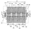
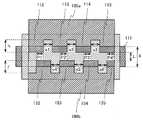
对于在本实施例中所例示的具有包括设法改变了源电极层和漏电极层的形状的结构A的晶体管,参照图1A来进行说明,并参照图1B说明其截面结构。另外,图1B所示的截面图对应于图1A中的剖线A1-A2处的截面图。如图1B所示,晶体管121设置在衬底100上并且具有栅电极层111、与栅电极层111接触的栅极绝缘层102、隔着栅极绝缘层102与栅电极层111重叠的半导体层106、以及其边缘各与半导体层106的一侧接触并且其边缘各隔着栅极绝缘层102与栅电极层111重叠的源电极层105a及漏电极层105b。Referring to FIG. 1A , a transistor having a structure A including a shape of a source electrode layer and a drain electrode layer exemplified in this embodiment will be described, and its cross-sectional structure will be described with reference to FIG. 1B . In addition, the cross-sectional view shown in FIG. 1B corresponds to the cross-sectional view at the section line A1 - A2 in FIG. 1A . As shown in FIG. 1B , the
图1A示出结构A的晶体管的示意性俯视图。源电极层105a具有以预定间隔s1、s2、s3隔开的相邻设置的多个电极齿形部分112、113、114、115以及使该电极齿形部分连接的连接部分116。FIG. 1A shows a schematic top view of a structure A transistor. The
漏电极层105b具有以预定间隔s4、s5、s6隔开的相邻设置的多个电极齿形部分142、143、144、145以及使该电极齿形部分连接的连接部分146。The
源电极层105a和漏电极层105b设置为使得源电极层105a的电极齿形部分112、113、114、115和漏电极层105b的电极齿形部分142、143、144、145彼此相对但不彼此交错。The
电极齿形部分112的端部和电极齿形部分142的端部设置为以相同的长度(P1)彼此相对。电极齿形部分113的端部和电极齿形部分143的端部设置为以相同的长度(P2)彼此相对。电极齿形部分114的端部和电极齿形部分144的端部设置为以相同的长度(P3)彼此相对。电极齿形部分115的端部和电极齿形部分145的端部设置为以相同的长度(P4)彼此相对。An end of the
此外,源电极层105a的端部和漏电极层105b的端部之间的间隔例如为3μm以上。这是为了防止因电极层之间的接触而发生短路等的缺陷。In addition, the distance between the end of the
此外,源电极层105a和漏电极层105b也分别可以通过层叠多个层来形成。In addition, the
如图1A所示,源电极层105a的各电极齿形部分112、113、114、115以及漏电极层105b的各电极齿形部分142、143、144、145以确保使它们的一部分隔着半导体层106与栅电极层111重叠的方式分别设置有重叠部分120、150。此外,也可以使源电极层105a的各电极齿形部分112、113、114、115的整个面积以及漏电极层105b的各电极齿形部分142、143、144、145的整个面积与栅电极层111重叠。As shown in FIG. 1A, each electrode tooth-shaped
此外,源电极层(梳形电极层)105a的连接部分116设置为不与栅电极层111重叠,且漏电极层(梳形电极层)105b的连接部分146设置为不与栅电极层111重叠。In addition, the
源电极层105a的各电极齿形部分的延伸方向上的、源电极层105a的电极齿形部分112、113、114、115与栅电极层111的重叠部分120的长度a,以及漏电极层105b的各电极齿形部分的延伸方向上的、漏电极层105b的电极齿形部分142、143、144、145与栅电极层111的重叠部分150的长度b,例如各为1.5μm以上。这是因为,在将栅极宽度g固定的情况下,当重叠部分120的长度a(重叠部分150的长度b)过短时,源电极层105a的端部和漏电极层105b的端部之间的间隔L过长,产生如下问题,例如通态电流急剧下降,或因在源电极层105a(漏电极层105b)与栅电极层111的重叠部分120(重叠部分150)不能建立接触而使晶体管的电阻增大。另外,源电极层105a的各电极齿形部分与栅电极层111的重叠部分120的长度a可以比漏电极层105b的各电极齿形部分与栅电极层111的重叠部分150的长度b长或短。The length a of the overlapping
源电极层105a的各电极齿形部分112、113、114、115的上表面可以具有至少一个圆角;其一个侧面或两个侧面可以倾斜或弯曲。The upper surface of each electrode tooth-shaped
漏电极层105b的各电极齿形部分142、143、144、145的上表面可以具有至少一个圆角;其一个侧面或两个侧面可以倾斜或弯曲。The upper surface of each
源电极层105a的各电极齿形部分112、113、114、115的长度h和漏电极层105b的各电极齿形部分142、143、144、145的长度i可以相同或不同。The length h of each
源电极层105a的电极齿形部分112-113之间的间隔(s1)、电极齿形部分113-114之间的间隔(s2)和电极齿形部分114-115之间的间隔(s3),以及漏电极层105b的电极齿形部分142-143之间的间隔(s4)、电极齿形部分143-144之间的间隔(s5)和电极齿形部分144-145之间的间隔(s6)都优选大于0μm且为5μm以下。尤其是,为了确保降低寄生电容,间隔s1、间隔s2、间隔s3、间隔s4、间隔s5、间隔s6优选大于3μm且为5μm以下。再者,为了将通态电流的下降抑制在允许范围内,该间隔优选分别为沟道形成区的长度(源电极层105a的端部和漏电极层105b的端部之间的间隔L)以下。the interval (s1) between the electrode serrations 112-113 of the
源电极层105a(梳形电极层)的端部的宽度优选为该源电极层105a的宽度w1的3/8以上且1/1以下,并且是漏电极层105b的宽度w2的3/8以上且8/3以下。The width of the end portion of the
漏电极层105b(梳形电极层)的端部的宽度优选为该漏电极层105b的宽度w2的3/8以上且1/1以下,并且是源电极层105a的宽度w1的3/8以上且8/3以下。The width of the end portion of the
另外,如图2A所示(结构B),电极齿形部分112、113、114、115的端部和电极齿形部分152、153、154、155的端部也可以设置为分别沿与电极齿形部分112、113、114、115或电极齿形部分152、153、154、155的端部长度不同的长度彼此相对(P1’、P2’、P3’和P4’)(例如,彼此不对准)。In addition, as shown in FIG. 2A (structure B), the ends of the electrode toothed
在此情况下,源电极层105a的电极齿形部分112-113之间的间隔(s1)、电极齿形部分113-114之间的间隔(s2)和电极齿形部分114-115之间的间隔(s3),以及漏电极层106b的电极齿形部分152-153之间的间隔(s4’)、电极齿形部分153-154之间的间隔(s5’)和电极齿形部分154-155之间的间隔(s6’)可以相同或不同,并且,源电极层105a的各电极齿形部分112、113、114、115的长度h与漏电极层106b的各电极齿形部分152、153、154、155的长度i’可以相同或不同。In this case, the interval (s1) between the electrode serrations 112-113 of the
另外,如图2B(结构C)所示,还可以采用矩形的漏电极层107b。In addition, as shown in FIG. 2B (structure C), a rectangular
接着,与现有的晶体管进行对比来说明这样的晶体管,其中,源电极层和漏电极层具有设计的新形状,可以大致保持通态电流,而降低在源电极层(漏电极层)与栅电极层的重叠部分产生的寄生电容。Next, a transistor in which the source electrode layer and the drain electrode layer have a newly designed shape that can roughly maintain the on-state current while reducing the difference between the source electrode layer (drain electrode layer) and the gate electrode layer will be described in comparison with the existing transistor. The parasitic capacitance generated by the overlapping part of the electrode layer.
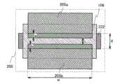
图3A示出现有的晶体管200的示意性俯视图的一个例子,而图3B示出具有新的电极形状的晶体管201(结构A)的示意性俯视图的一个例子。另外,晶体管200和晶体管201的截面结构与图1B所示的结构A的晶体管121的截面结构相同。FIG. 3A shows an example of a schematic top view of a
图3A示出源电极层205a、漏电极层205b、栅电极层222和半导体层106。图3B示出源电极层206a、漏电极层206b、栅电极层222和半导体层106。FIG. 3A shows a
注意,源电极层205a(漏电极层205b)的宽度w和源电极层206a(漏电极层206b)的宽度w’相同;源电极层205a与栅电极层222的重叠部分的长度a、漏电极层205b与栅电极层222的重叠部分的长度b、源电极层(梳形电极层)206a的各电极齿形部分与栅电极层222的重叠部分的长度a’以及漏电极层(梳形电极层)206b的各电极齿形部分与栅电极层222的重叠部分的长度b’相同;并且,源电极层205a的边缘与漏电极层205b的边缘之间的间隔L以及源电极层206a的端部与漏电极层206b的端部之间的间隔L’相同。Note that the width w of the
如图3A和3B所示,可以使晶体管201的源电极层206a(漏电极层206b)与栅电极层222的重叠部分的面积小于晶体管200的源电极层205a(漏电极层205b)与栅电极层222的重叠部分的面积。As shown in FIGS. 3A and 3B , the area of the overlapping portion of the
例如,若图3B所示的源电极层206a(漏电极层206b)的各电极齿形部分的长度都相同,源电极层206a(漏电极层206b)的各电极齿形部分的宽度都相同,并且各电极齿形部分之间的间隔都相同,则可以使源电极层206a(漏电极层206b)与栅电极层222的重叠部分的面积成为图3A所示的源电极层205a(漏电极层205b)与栅电极层222的重叠部分的面积的大约一半。For example, if the lengths of the electrode serrations of the
因此,通过将源(漏)电极层的形状从矩形改变为梳形,可以降低在重叠部分产生的寄生电容。Therefore, by changing the shape of the source (drain) electrode layer from a rectangle to a comb shape, the parasitic capacitance generated at the overlapping portion can be reduced.
图4A示出晶体管200的电流通路的示意性俯视图的一个例子,而图4B示出晶体管201(结构A)的电流通路的示意性俯视图的一个例子。FIG. 4A shows an example of a schematic top view of the current path of
如图4A所示,在晶体管200中,线性电流从源电极层205a的边缘流向漏电极层205b的边缘。另一方面,如图4B所示,在晶体管201中,线性电流从源电极层206a的各电极齿形部分212、213、214、215的端部流向漏电极层206b的各电极齿形部分242、243、244、245的端部,而且线性电流从源电极层206a的连接部分216的边缘流向漏电极层206b的连接部分246的边缘。晶体管201中的线性电流量比晶体管200中的线性电流量小。这是因为如下缘故:因连接部分216(连接部分246)与栅电极层222彼此不重叠而使电阻增大,由此从连接部分216的边缘流向连接部分246的边缘的线性电流减小。As shown in FIG. 4A, in the
然而,如图4B所示,在晶体管201中,曲线电流从源电极层206a的各电极齿形部分212、213、214、215的侧边流向漏电极层206b的各电极齿形部分242、243、244、245的侧边,以补偿与晶体管200相比更小的线性电流。据此,可以使晶体管200中的线性电流量与晶体管201中的线性电流和曲线电流的总量大致相同。However, as shown in FIG. 4B, in the
在图4A所示的晶体管200中,当将栅极宽度g固定时,通过减少源电极层205a与栅电极层222的重叠部分的长度a(漏电极层205b与栅电极层222的重叠部分的长度b),可以减少重叠部分的面积。但是此时,因为沟道形成区的长度L(源电极层205a的边缘与漏电极层205b的边缘之间的间隔L)与其同时增大,所以不能保持通态电流。In the
相反,通过将各电极层的形状从矩形的源电极层205a(漏电极层205b)改变为梳形的源电极层206a(漏电极层206b),可以不改变沟道形成区的长度地(意味着源电极层205a的边缘和漏电极层205b的边缘之间的间隔L与源电极层206a的端部和漏电极层206b的端部之间的间隔L’相同)减少重叠部分的面积。再者,因为此时可以产生从源电极层206a的各电极齿形部分的侧边流向漏电极层206b的各电极齿形部分的侧边以围绕各个电极齿形部分的曲线电流,所以即使沟道形成区的宽度减少,也可以保持通态电流不变。也就是说,晶体管201也可以与晶体管200同样地保持仅依赖于沟道形成区的长度的通态电流。On the contrary, by changing the shape of each electrode layer from the rectangular
因此,通过将源(漏)电极层的形状从矩形改变为梳形,在降低寄生电容的同时也可以大致保持通态电流。Therefore, by changing the shape of the source (drain) electrode layer from a rectangle to a comb shape, the on-state current can be substantially maintained while reducing the parasitic capacitance.
注意,在图3B和图4B所示的晶体管201中,当进一步扩大各电极齿形部分之间的间隔并且进一步扩大梳形电极层的端部之间的间隔时,虽然可以降低寄生电容,但是不能产生能够补偿降低的线性电流的、以围绕各电极齿形部分的方式流过的足量曲线电流。此时,通态电流急剧下降。因此,为了保持一定量以上的通态电流,各电极齿形部分之间的间隔及梳形电极层的端部之间的间隔需要设为一定值以下。Note that in the
通过采用如上所述的结构,可以提供在降低在源电极层(漏电极层)与栅电极层的重叠部分产生的寄生电容的同时可以大致保持通态电流的具有新的结构的晶体管。By adopting the structure as described above, it is possible to provide a transistor having a novel structure capable of substantially maintaining an on-state current while reducing parasitic capacitance generated at an overlapping portion of a source electrode layer (drain electrode layer) and a gate electrode layer.
另外,本实施例所示的各结构可以与其他实施例所例示的任意结构适当地组合来实施。In addition, each structure shown in this embodiment can be combined suitably with the arbitrary structure shown in other embodiment.
实施例2Example 2
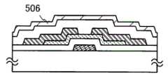
在本实施例中,参照图9A至9E对将氧化物半导体用作构成实施例1所说明的晶体管的半导体层的材料时的制造工序进行说明。另外,可以与上述实施例同样地形成与上述实施例相同的部分或具有类似功能的部分,并且可以与上述实施例同样地进行与上述实施例相同的工序,而省略重复说明。此外,不重复对于相同部分的详细说明。In this embodiment, the manufacturing process when an oxide semiconductor is used as the material of the semiconductor layer constituting the transistor described in
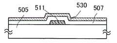
在下文中,将参照图9A至9E来说明在衬底505上制造晶体管510的工序。Hereinafter, the process of manufacturing the
首先,当在具有绝缘表面的衬底505上形成导电膜后,通过第一光刻工序形成栅电极层511。另外,也可以通过喷墨法形成抗蚀剂掩模。因为当通过喷墨法形成抗蚀剂掩模时不使用光掩模,所以可以降低制造成本。First, after forming a conductive film on a
在本实施例中,作为具有绝缘表面的衬底505使用玻璃衬底。In this embodiment, a glass substrate is used as the
也可以在衬底505和栅电极层511之间形成用作基底膜的绝缘膜。基底膜具有防止杂质元素从衬底505扩散的功能,该基底膜可以由选自氮化硅膜、氧化硅膜、氮氧化硅膜、氧氮化硅膜中的一种膜或多种膜的叠层结构形成。An insulating film serving as a base film may also be formed between the
此外,栅电极层511可以使用钼、钛、钽、钨、铝、铜、钕、钪等的金属材料或以任意这些金属材料为主要成分的合金材料以单层或叠层形成。In addition, the
接着,在栅电极层511上形成栅极绝缘层507。栅极绝缘层507可以通过等离子CVD法或溅射法等由氧化硅层、氮化硅层、氧氮化硅层、氮氧化硅层、氧化铝层、氮化铝层、氧氮化铝层、氮氧化铝层或氧化铪层的单层或叠层形成。Next, a
作为本实施例的氧化物半导体,使用通过去除杂质而i型化或实质上i型化的氧化物半导体。因为这种高纯度化的氧化物半导体对界面能级、界面电荷极敏感,所以氧化物半导体层和栅极绝缘层之间的界面是重要的。因此,与高纯度化的氧化物半导体接触的栅极绝缘层被要求高质量化。As the oxide semiconductor of this embodiment, an oxide semiconductor that has been made i-type or substantially i-type by removing impurities is used. Since such a highly purified oxide semiconductor is extremely sensitive to interface energy levels and interface charges, the interface between the oxide semiconductor layer and the gate insulating layer is important. Therefore, it is required to improve the quality of the gate insulating layer in contact with the highly purified oxide semiconductor.
例如,利用μ波(例如,频率为2.45GHz)的高密度等离子体CVD法可以形成致密且耐压性高的高质量绝缘层,所以是优选的。这是因为通过使高纯度化的氧化物半导体和高质量的栅极绝缘层密接,可以降低界面能级而获得良好的界面特性的缘故。For example, a high-density plasma CVD method using μ waves (for example, a frequency of 2.45 GHz) is preferable because it can form a dense and high-quality insulating layer with high voltage resistance. This is because the interface energy level can be lowered to obtain good interface characteristics by bringing a highly purified oxide semiconductor into close contact with a high-quality gate insulating layer.
当然,只要是可以形成优质绝缘层作为栅极绝缘层的方法,就可以应用溅射法、等离子体CVD法等的其他成膜方法。此外,也可以采用通过成膜后的热处理改善了膜质量的栅极绝缘层及改善了其与氧化物半导体之间的界面特性的绝缘层。总之,只要采用作为栅极绝缘层的膜质量良好,并且可以降低界面能级密度而形成与氧化物半导体之间的良好的界面的绝缘层即可。Of course, other film-forming methods such as sputtering and plasma CVD can be applied as long as a high-quality insulating layer can be formed as the gate insulating layer. In addition, a gate insulating layer whose film quality has been improved by heat treatment after film formation and an insulating layer whose interface properties with an oxide semiconductor have been improved may also be used. In short, it is sufficient to use an insulating layer that has a good film quality as the gate insulating layer and can reduce the interface level density to form a good interface with the oxide semiconductor.
此外,为了尽可能不使栅极绝缘层507、氧化物半导体膜530包含氢、羟基和水分,在形成氧化物半导体膜530之前,优选在溅射装置的预备加热室中对形成有栅电极层511的衬底505或形成有栅电极层511和栅极绝缘层507的衬底505进行预备加热,来使吸附在衬底505上的氢、水分等的杂质脱附并排空。另外,作为设置在预备加热室中的排空单元,优选使用低温泵。另外,也可以省略该预备加热工序。此外,也可以同样地在形成绝缘层516之前对形成有直到并包括源电极层515a和漏电极层515b的部件的衬底505进行该预备加热工序。In addition, in order to prevent the
接着,在栅极绝缘层507上形成厚度为2nm以上且200nm以下,优选为5nm以上且30nm以下的氧化物半导体膜530(参照图9A)。Next, an
另外,优选的是,在通过溅射法形成氧化物半导体膜530之前,进行引入氩气体而产生等离子体的反溅射,来去除附着在栅极绝缘层507表面上的粉状物质(也称为微粒、尘屑)。反溅射是如下一种方法:不对靶材一侧施加电压,而在氩气氛下使用RF电源对衬底一侧施加电压来在衬底附近形成等离子体,由此进行表面改性。另外,也可以使用氮、氦、氧等而代替氩气氛。In addition, it is preferable to perform reverse sputtering in which argon gas is introduced to generate plasma before forming the
作为形成氧化物半导体膜530的氧化物半导体,可以使用作为四元金属氧化物的In-Sn-Ga-Zn-O类氧化物半导体;作为三元金属氧化物的In-Ga-Zn-O类氧化物半导体、In-Sn-Zn-O类氧化物半导体、In-Al-Zn-O类氧化物半导体、Sn-Ga-Zn-O类氧化物半导体、Al-Ga-Zn-O类氧化物半导体、Sn-Al-Zn-O类氧化物半导体;作为二元金属氧化物的In-Zn-O类氧化物半导体、Sn-Zn-O类氧化物半导体、Al-Zn-O类氧化物半导体、Zn-Mg-O类氧化物半导体、Sn-Mg-O类氧化物半导体、In-Mg-O类氧化物半导体;或者作为单元氧化物半导体的In-O类氧化物半导体、Sn-O类氧化物半导体、Zn-O类氧化物半导体等。此外,也可以使上述氧化物半导体包含SiO2。在此,例如,In-Ga-Zn-O类氧化物半导体是指具有铟(In)、镓(Ga)、锌(Zn)的氧化物,并且对其化学计量比并没有限制。此外,氧化物半导体也可以包含In、Ga、Zn以外的元素。在本实施例中,使用In-Ga-Zn-O类金属氧化物靶材通过溅射法形成氧化物半导体膜530。此阶段的截面图为图9A。As the oxide semiconductor forming the
作为用于通过溅射法形成氧化物半导体膜530的靶材,例如使用组成比为In2O3:Ga2O3:ZnO=1:1:1[摩尔比]的氧化物靶材,来形成In-Ga-Zn-O膜。此外,不局限于上述靶材的材料和组成,例如也可以使用组成比为In2O3:Ga2O3:ZnO=1:1:2[摩尔比]的氧化物靶材。As a target for forming the
此外,氧化物靶材的填充率为90%以上且100%以下,优选为95%以上且99.9%以下。通过使用高填充率的金属氧化物靶材,可以形成致密的氧化物半导体膜。In addition, the filling rate of the oxide target is 90% to 100%, preferably 95% to 99.9%. A dense oxide semiconductor film can be formed by using a metal oxide target with a high filling rate.
作为在形成氧化物半导体膜530时使用的溅射气体,优选使用去除了氢、水、羟基或氢化物等的杂质的高纯度气体。As the sputtering gas used when forming the
在保持为减压状态的成膜室中固定衬底,将衬底温度设定为100℃以上且600℃以下,优选设定为200℃以上且400℃以下。通过一边加热衬底一边进行成膜,可以降低包含在氧化物半导体膜中的杂质浓度。此外,可以减轻由溅射引起的损伤。然后,在去除了残留水分的成膜室内引入去除了氢和水分的溅射气体,使用上述靶材在衬底505上形成氧化物半导体膜530。为了去除成膜室内的残留水分,优选使用捕集真空泵,例如低温泵、离子泵、钛升华泵。此外,作为排空单元,也可以使用配备有冷阱的涡轮泵。因为在使用低温泵进行排空的成膜室中,例如对氢原子、水(H2O)等的包含氢原子的化合物(更优选的是,还对包含碳原子的化合物)等进行排空,所以可以降低在该成膜室中形成的氧化物半导体膜所包含的杂质的浓度。The substrate is fixed in the film-forming chamber kept in a depressurized state, and the substrate temperature is set to 100°C to 600°C, preferably 200°C to 400°C. By forming the film while heating the substrate, the impurity concentration contained in the oxide semiconductor film can be reduced. In addition, damage caused by sputtering can be mitigated. Then, a sputtering gas from which hydrogen and moisture have been removed is introduced into the film formation chamber from which residual moisture has been removed, and an
作为进行溅射法的气氛,采用稀有气体(典型为氩)气氛、氧气氛或稀有气体和氧的混合气氛,即可。As an atmosphere for performing the sputtering method, a rare gas (typically argon) atmosphere, an oxygen atmosphere, or a mixed atmosphere of a rare gas and oxygen may be used.
作为成膜条件的一个例子,采用如下条件:衬底和靶材之间的距离为100mm;压力为0.6Pa;直流(DC)功率为0.5kW;以及利用氧(氧流量比率为100%)气氛。另外,脉冲直流电源是优选的,因为可以减轻在进行成膜时产生的粉状物质(也称为微粒、尘屑),并且膜厚度也变得均匀。As an example of the film formation conditions, the following conditions are employed: the distance between the substrate and the target is 100mm; the pressure is 0.6Pa; the direct current (DC) power is 0.5kW; and an atmosphere using oxygen (oxygen flow ratio is 100%) . In addition, a pulsed DC power supply is preferable because powdery substances (also referred to as fine particles, dust) generated when film formation is performed can be reduced, and the film thickness also becomes uniform.
接着,通过第二光刻工序将氧化物半导体膜530加工为岛状氧化物半导体层。此外,也可以通过喷墨法形成用来形成岛状氧化物半导体层的抗蚀剂掩模。因为当通过喷墨法形成抗蚀剂掩模时不使用光掩模,所以可以降低制造成本。Next, the
此外,当在栅极绝缘层507中形成接触孔时,可以在进行氧化物半导体膜530的加工时同时进行该工序。In addition, when forming a contact hole in the
另外,作为对氧化物半导体膜530进行的蚀刻,可以采用干蚀刻和湿蚀刻中的一方或者双方。例如,作为对氧化物半导体膜530进行湿蚀刻时使用的蚀刻剂,可以使用混合有磷酸、醋酸、硝酸的溶液等。此外,也可以使用ITO-07N(由日本关东化学株式会社制造)。In addition, as etching of the
接着,对氧化物半导体层进行第一加热处理。通过该第一加热处理,可以使氧化物半导体层脱水化或脱氢化。将第一加热处理的温度设定为400℃以上且750℃以下,或者400℃以上且低于衬底的应变点。在此,将衬底引入到加热处理装置之一的电炉中,在氮气氛下以450℃的温度对氧化物半导体层进行1小时的加热处理,然后不使该氧化物半导体层接触于大气而防止水、氢再次混入到其中,以得到氧化物半导体层531(参照图9B)。Next, a first heat treatment is performed on the oxide semiconductor layer. By this first heat treatment, the oxide semiconductor layer can be dehydrated or dehydrogenated. The temperature of the first heat treatment is set to be 400° C. or higher and 750° C. or lower, or 400° C. or higher and lower than the strain point of the substrate. Here, the substrate was introduced into an electric furnace which is one of the heat treatment devices, the oxide semiconductor layer was heat-treated at 450° C. for 1 hour in a nitrogen atmosphere, and then the oxide semiconductor layer was heated without exposing the oxide semiconductor layer to the atmosphere. Water and hydrogen are prevented from being re-mixed thereinto to obtain an oxide semiconductor layer 531 (see FIG. 9B ).
另外,加热处理装置不局限于电炉,也可以使用利用来自电阻发热体等的发热体的热传导或热辐射对处理对象进行加热的装置。例如,可以使用如GRTA(Gas Rapid Thermal Anneal,即气体快速热退火)装置、LRTA(Lamp Rapid Thermal Anneal,即灯快速热退火)装置等的RTA(Rapid Thermal Anneal,即快速热退火)装置。LRTA装置是利用卤素灯、金卤灯、氙弧灯、碳弧灯、高压钠灯、或者高压汞灯等的灯所发出的光(电磁波)的辐射对处理对象进行加热的装置。GRTA装置是利用高温气体进行加热处理的装置。作为高温气体,使用如氩等的稀有气体或氮等的即使进行加热处理也不与处理对象起反应的惰性气体。In addition, the heat treatment apparatus is not limited to an electric furnace, and an apparatus that heats an object to be treated by heat conduction or heat radiation from a heating element such as a resistance heating element may also be used. For example, an RTA (Rapid Thermal Anneal) device such as a GRTA (Gas Rapid Thermal Anneal) device, an LRTA (Lamp Rapid Thermal Anneal, lamp rapid thermal anneal) device, etc. may be used. The LRTA device is a device that heats the object to be treated by radiation of light (electromagnetic waves) emitted by lamps such as halogen lamps, metal halide lamps, xenon arc lamps, carbon arc lamps, high-pressure sodium lamps, or high-pressure mercury lamps. The GRTA device is a device for heat treatment using high-temperature gas. As the high-temperature gas, a rare gas such as argon, or an inert gas such as nitrogen that does not react with a processing object even when heat-treated is used.
例如,作为第一加热处理可以进行GRTA,其中将衬底移动到加热到650℃至700℃的高温的惰性气体中,加热几分钟,然后移动并将衬底从加热到高温的惰性气体中取出。For example, GRTA may be performed as the first heat treatment in which the substrate is moved into an inert gas heated to a high temperature of 650°C to 700°C, heated for a few minutes, and then moved and taken out of the inert gas heated to a high temperature .
另外,在第一加热处理中,氮或诸如氦、氖、氩等的稀有气体优选不包含水、氢等。或者,优选将引入到加热处理装置中的氮或诸如氦、氖、氩等的稀有气体的纯度设定为6N(99.9999%)以上,更优选设定为7N(99.99999%)以上(即,将杂质浓度设定为1ppm以下,优选设定为0.1ppm以下)。In addition, in the first heat treatment, nitrogen or a rare gas such as helium, neon, argon, or the like preferably does not contain water, hydrogen, or the like. Alternatively, it is preferable to set the purity of nitrogen or a rare gas such as helium, neon, argon, etc. introduced into the heat treatment device to be 6N (99.9999%) or higher, more preferably 7N (99.99999%) or higher (that is, to The impurity concentration is set to 1 ppm or less, preferably 0.1 ppm or less).
此外,也可以在通过第一加热处理加热氧化物半导体层之后,对相同的炉中引入高纯度的氧气体、高纯度的N2O气体或超干燥气体(露点为-40℃以下,优选为-60℃以下)。氧气体或N2O气体优选不包含水、氢等。或者,优选将引入到加热处理装置中的氧气体或N2O气体的纯度设定为6N以上,更优选设定为7N以上(即,将氧气体或N2O气体中的杂质浓度设定为1ppm以下,优选设定为0.1ppm以下)。通过利用氧气体或N2O气体的作用,供应当进行在通过脱水化或脱氢化去除杂质的工序的同时减少的、构成氧化物半导体的主要成分之一的氧,可以使氧化物半导体层高纯度化及电性i型(本征)化。In addition, it is also possible to introduce high-purity oxygen gas, high-purity N2 O gas, or ultra-dry gas (with a dew point of -40° C. or lower, preferably below -60°C). Oxygen gas or N2 O gas preferably does not contain water, hydrogen, or the like. Alternatively, it is preferable to set the purity of the oxygen gas orN2O gas introduced into the heat treatment device to be 6N or higher, more preferably 7N or higher (that is, the impurity concentration in the oxygen gas orN2O gas is set to 1 ppm or less, preferably 0.1 ppm or less). By utilizing the action of oxygen gas or N2 O gas, supplying oxygen, which is one of the main components of the oxide semiconductor, which is reduced while performing the process of removing impurities by dehydration or dehydrogenation, can make the oxide semiconductor layer high Purification and electrical i-type (intrinsic).
此外,也可以对加工为岛状氧化物半导体层之前的氧化物半导体膜530进行氧化物半导体层的第一加热处理。在此情况下,在第一加热处理之后从加热装置中取出衬底并进行光刻工序。In addition, the first heat treatment of the oxide semiconductor layer may be performed on the
另外,除了上述定时之外,只要在形成氧化物半导体层之后,就还可以在以下的任意定时进行第一加热处理,该定时例如将源电极层和漏电极层形成在氧化物半导体层上之后或在将绝缘层形成在源电极层和漏电极层上之后。In addition, in addition to the above-mentioned timing, the first heat treatment may be performed at any timing as long as after the oxide semiconductor layer is formed, for example, after the source electrode layer and the drain electrode layer are formed on the oxide semiconductor layer Or after an insulating layer is formed on the source electrode layer and the drain electrode layer.
此外,当在栅极绝缘层507中形成接触孔时,在对氧化物半导体膜530进行第一加热处理之前或之后都可以进行该接触孔的形成。Furthermore, when forming a contact hole in the
此外,也可以通过分两次形成氧化物半导体层,并分两次进行加热处理,由此形成的氧化物半导体层具有较厚的结晶区(单晶区),即其c轴沿垂直于层表面的方向取向的结晶区,不论基底构件的材料是氧化物、氮化物、还是金属等。例如,形成3nm以上且15nm以下的厚度第一氧化物半导体膜,并且在氮、氧、稀有气体或干燥空气的气氛下以450℃以上且850℃以下的温度,优选以550℃以上且750℃以下的温度进行第一加热处理,来形成在包括表面的区域中具有结晶区(包括板状结晶)的第一氧化物半导体膜;然后,形成厚于第一氧化物半导体膜的第二氧化物半导体膜,并且以450℃以上且850℃以下的温度,优选以600℃以上且700℃以下的温度进行第二加热处理,以第一氧化物半导体膜为晶体生长的种子使结晶向上方生长,来使第二氧化物半导体膜整体晶化。按这种方式来形成具有较厚的结晶区的氧化物半导体层。In addition, it is also possible to form the oxide semiconductor layer twice and perform the heat treatment twice, so that the formed oxide semiconductor layer has a thicker crystalline region (single crystal region), that is, its c-axis is perpendicular to the layer A crystalline region oriented in the direction of the surface, regardless of whether the material of the base member is oxide, nitride, or metal. For example, the first oxide semiconductor film is formed to have a thickness of 3 nm or more and 15 nm or less, and at a temperature of 450° C. to 850° C., preferably 550° C. or more and 750° C. The first heat treatment is performed at a temperature below to form a first oxide semiconductor film having a crystalline region (including plate crystals) in a region including the surface; then, a second oxide thicker than the first oxide semiconductor film is formed semiconductor film, and the second heat treatment is performed at a temperature of 450° C. to 850° C., preferably at a temperature of 600° C. to 700° C. to grow crystals upward using the first oxide semiconductor film as a seed for crystal growth, to crystallize the entire second oxide semiconductor film. In this way, an oxide semiconductor layer having a thick crystal region is formed.
接着,在栅极绝缘层507和氧化物半导体层531上形成成为源电极层和漏电极层(包括由与源电极层和漏电极层相同的层形成的布线)的导电膜。作为用于源电极层和漏电极层的导电膜,例如可以使用含有选自Al、Cr、Cu、Ta、Ti、Mo、W中的元素的金属膜或含有任意上述元素为成分的金属氮化物膜(氮化钛膜、氮化钼膜、氮化钨膜)等。此外,还可以在Al、Cu等的金属膜的下侧和上侧的一方或双方层叠Ti、Mo、W等的高熔点金属膜或任意这些元素的金属氮化物膜(氮化钛膜、氮化钼膜、氮化钨膜)的结构。特别优选的是,在与氧化物半导体层接触的一侧设置含有钛的导电膜。Next, a conductive film to be a source electrode layer and a drain electrode layer (including wiring formed of the same layer as the source electrode layer and the drain electrode layer) is formed on the
通过第三光刻工序在导电膜上形成抗蚀剂掩模,并且选择性地进行蚀刻来形成源电极层515a和漏电极层515b,然后去除抗蚀剂掩模(参照图9C)。A resist mask is formed on the conductive film by a third photolithography process, and etching is selectively performed to form a
另外,源电极层515a和漏电极层515b的形状为梳形,并且在氧化物半导体层531上延伸存在的各电极齿形部的至少其一部分与栅电极层511重叠。In addition, the
通过将源电极层515a和漏电极层515b形成为梳形,可以减少源电极层515a(漏电极层515b)与栅电极层511彼此重叠的部分的面积,由此可以降低寄生电容。By forming the
此外,如图9C所示,通过将梳形的源电极层515a和漏电极层515b设置为其各电极齿形部分彼此相对,可以产生从源电极层515a的电极齿形部分的侧边流向漏电极层515b的电极齿形部分的侧边的围绕各电极齿形部分的曲线电流。通过利用该曲线电流(间接电流),可以防止通态电流的下降。In addition, as shown in FIG. 9C, by arranging the comb-shaped
作为通过第三光刻工序形成抗蚀剂掩模时的曝光,优选使用紫外线、KrF激光或ArF激光来进行。待形成的晶体管的沟道长度L取决于氧化物半导体层531上彼此相邻的源电极层的下边缘和漏电极层的下边缘之间的间隔宽度。另外,当进行对于短于25nm的沟道长度L曝光时,优选使用具有几nm至几十nm的极短波长的超紫外线(Extreme Ultraviolet)进行在通过第三光刻工序形成抗蚀剂掩模时的曝光。利用超紫外线的曝光的分辨率高且聚焦深度大。因此,也可以使晶体管的沟道长度L设定为10nm以上且1000nm以下,这样可以实现电路的工作速度的高速化。Exposure when forming a resist mask in the third photolithography step is preferably performed using ultraviolet rays, KrF lasers, or ArF lasers. The channel length L of the transistor to be formed depends on the space width between the lower edge of the source electrode layer and the lower edge of the drain electrode layer adjacent to each other on the
另外,优选使蚀刻条件最优化,以便防止当对导电膜进行蚀刻时氧化物半导体层531被蚀刻并分割。然而,难以获得只对导电膜进行蚀刻而完全不对氧化物半导体层531进行蚀刻的条件。因此,有可能当对导电膜进行蚀刻时氧化物半导体层531的仅仅一部分被蚀刻而成为具有槽部(凹部)的氧化物半导体层。In addition, it is preferable to optimize the etching conditions in order to prevent the
在本实施例中,因为将Ti膜用作导电膜并将In-Ga-Zn-O类氧化物半导体用于氧化物半导体层531,所以作为Ti膜的蚀刻剂使用氨水-过氧化氢混合液(31重量%过氧化氢溶液:28重量%氨水:水=5:2:2)。In this embodiment, since a Ti film is used as a conductive film and an In-Ga-Zn-O-based oxide semiconductor is used for the
接着,也可以进行使用N2O、N2或Ar等的气体的等离子体处理,去除附着在露出的氧化物半导体层表面上的水等。当进行等离子体处理时,不接触于大气地形成与氧化物半导体层的一部分接触的用作保护绝缘层的绝缘层516。Next, plasma treatment using gas such as N2 O, N2 , or Ar may be performed to remove water or the like adhering to the exposed surface of the oxide semiconductor layer. When the plasma treatment is performed, the insulating
绝缘层516至少具有1nm以上的厚度,并且可以适当地采用溅射法等的不使水、氢等的杂质混入到绝缘层516中的方法来形成。当绝缘层516包含氢时,有如下忧虑:因氢侵入到氧化物半导体层中或氢抽出氧化物半导体层中的氧而使氧化物半导体层的背沟道低电阻化(N型化),由此形成寄生沟道。因此,重要的是,采用其中不使用氢的成膜方法,以使绝缘层516尽量少包含氢。The insulating
在本实施例中,作为绝缘层516通过溅射法形成厚度为200nm的氧化硅膜。将成膜时的衬底温度设定为室温以上且300℃以下即可,在本实施例中将其设定为100℃。可以在稀有气体(典型的是氩)气氛下、氧气氛下或稀有气体和氧的混合气氛下通过溅射法形成氧化硅膜。此外,作为靶材可以使用氧化硅靶材或硅靶材。例如,可以使用硅靶材在包含氧的气氛下通过溅射法形成氧化硅膜。作为形成为与氧化物半导体层接触的绝缘层516,使用不包含水分、氢离子、OH-等的杂质并阻挡这些杂质从外部侵入的无机绝缘膜,典型地使用氧化硅膜、氧氮化硅膜、氧化铝膜或氧氮化铝膜等。In this embodiment, as the insulating
与形成氧化物半导体膜530时同样,优选使用捕集真空泵(低温泵等)去除用于形成绝缘层516的成膜室中的残留水分。在使用低温泵排空的成膜室中形成绝缘层516时,可以降低绝缘层516中的杂质的浓度。此外,作为用来去除用于形成绝缘层516的成膜室中的残留水分的排空单元,也可以使用配备有冷阱的涡轮泵。As in the case of forming the
作为当形成绝缘层516时使用的溅射气体,优选使用减少了氢、水、羟基或氢化物等的杂质的高纯度气体。As the sputtering gas used when forming the insulating
接着,在惰性气体气氛下或氧气气氛下进行第二加热处理(优选为200℃以上且400℃以下,例如250℃以上且350℃以下)。例如,在氮气氛下以250℃的温度进行1小时的第二加热处理。当进行第二加热处理时,氧化物半导体层的一部分(沟道形成区)在与绝缘层516接触的状态下被加热。Next, a second heat treatment (preferably not less than 200° C. and not more than 400° C., for example, not less than 250° C. and not more than 350° C.) is performed under an inert gas atmosphere or an oxygen atmosphere. For example, the second heat treatment is performed at a temperature of 250° C. for 1 hour in a nitrogen atmosphere. When the second heat treatment is performed, a part of the oxide semiconductor layer (channel formation region) is heated in a state of being in contact with the insulating
通过上述工序,可以对氧化物半导体膜进行第一加热处理而从氧化物半导体层中意图排除氢、水分、羟基或氢化物(也称为氢化合物)等的杂质,并且可以供应当进行杂质的排除工序时同时减少的构成氧化物半导体的主要成分之一的氧。因此,氧化物半导体层被高纯度化和电性i型(本征)化。Through the above steps, the oxide semiconductor film can be subjected to the first heat treatment to remove impurities such as hydrogen, water, hydroxyl groups, or hydrides (also called hydrogen compounds) from the oxide semiconductor layer, and it is possible to supply Oxygen, which is one of the main components of the oxide semiconductor, is reduced at the same time as the removal process. Therefore, the oxide semiconductor layer is highly purified and electrically i-type (intrinsic).
以上述工序形成晶体管510(参照图9D)。The
此外,当作为绝缘层516使用包括很多缺陷的氧化硅层时,通过在形成氧化硅层之后进行的加热处理将包含在氧化物半导体层中的氢、水分、羟基或氢化物等的杂质扩散到氧化物绝缘层中,而进一步减少包含在氧化物半导体层中的该杂质。Furthermore, when a silicon oxide layer including many defects is used as the insulating
也可以在绝缘层516上还形成保护绝缘层506。例如,作为保护绝缘层506,通过RF溅射法形成氮化硅膜。因为RF溅射法的批量生产性高,所以作为保护绝缘层的成膜方法,优选使用RF溅射法。作为保护绝缘层,使用不包含水分等的杂质并阻挡这些杂质从外部侵入的无机绝缘膜来形成,例如使用氮化硅膜、氮化铝膜等。在本实施例中,使用氮化硅膜形成保护绝缘层506(参照图9E)。The protective
在本实施例中,作为保护绝缘层506,将设置有部件并包括绝缘层516的衬底505加热到100℃至400℃时,引入包含其中氢和水分被减少的高纯度氮的溅射气体并使用硅半导体的靶材形成氮化硅膜。在此情况下,也优选与形成绝缘层516时同样地在形成保护绝缘层506的期间去除处理室中的残留水分。In this embodiment, as the protective insulating
在形成保护绝缘层之后,还可以在大气中以100℃以上且200℃以下的温度进行1小时以上且30小时以下的加热处理。在该加热处理中,既可以保持固定的加热温度进行热处理,又可以多次反复进行加热温度的如下改变:加热温度从室温升到100℃以上且200℃以下的温度降低到室温。After forming the protective insulating layer, heat treatment may be performed in the air at a temperature of 100° C. to 200° C. for 1 hour to 30 hours. In this heat treatment, the heat treatment can be performed while maintaining a fixed heating temperature, or the following change of the heating temperature can be repeated several times: the heating temperature is raised from room temperature to a temperature above 100°C and lowered to room temperature below 200°C.
通过将氧化物半导体用于本实施例所例示的晶体管,可以得到高电场效应迁移率,从而可以实现高速工作。此外,因为源电极层515a(漏电极层515b)具有梳形,所以可以在降低源电极层515a(漏电极层515b)与栅电极层511之间产生的寄生电容的同时实现高速工作。再者,施加到栅电极层511的信号的畸变减轻到不用顾及的程度,从而可以使包括氧化物半导体的晶体管电路以高频率工作。By using an oxide semiconductor for the transistor exemplified in this embodiment, high field-effect mobility can be obtained and high-speed operation can be realized. Furthermore, since the
包括这种晶体管的各种装置可以实现低耗电工作和高速工作。可以说,这可以扩大例如在液晶显示装置中将驱动器安装在更大的面板、更高清晰度的面板中的可能性。Various devices including such transistors can realize low power consumption operation and high-speed operation. It can be said that, for example, in a liquid crystal display device, it is possible to mount a driver in a larger panel and a higher-definition panel.
另外,本实施例所示的各结构可以与其他实施例所例示的任意结构适当地组合来实施。In addition, each structure shown in this embodiment can be combined suitably with the arbitrary structure shown in other embodiment.
在下面所示的示例中对具有上述结构的本发明进行更详细的说明。The present invention having the above-mentioned structure will be described in more detail in the examples shown below.
示例1Example 1
在本示例中,制造了实施例1所例示的设法改变了源电极层和漏电极层的形状的晶体管。根据实验具体证明如下事实,即所制造的晶体管在源电极层(漏电极层)与栅电极层的重叠部分产生的寄生电容降低时,也可以大致保持通态电流。In this example, a transistor in which the shapes of the source electrode layer and the drain electrode layer were contrived to be changed as exemplified in
将示出本示例中的各晶体管的详细截面结构。在玻璃衬底上形成了基底膜。基底膜通过层叠两个层而形成,这两个层为厚度为100nm的氮化硅膜和厚度为150nm的氧氮化硅膜。在基底膜上形成了栅电极层。作为栅电极层使用钨(W),并将其厚度设定为100nm。在栅电极层上形成了栅极绝缘膜。作为栅极绝缘膜使用氧氮化硅膜,并将其厚度设定为100nm。此外,形成了隔着栅极绝缘膜与栅电极层重叠的氧化物半导体膜。作为氧化物半导体膜使用IGZO,并将其厚度设定为15nm。再者,以使其边缘与氧化物半导体膜接触并且与栅电极层重叠的方式形成了源电极层和漏电极层。源电极层和漏电极层通过层叠钛(Ti)、铝(Al)、钛(Ti)的三层而形成,并将它们的厚度分别设定为50nm、200nm、50nm。A detailed cross-sectional structure of each transistor in this example will be shown. A base film was formed on the glass substrate. The base film is formed by laminating two layers, a silicon nitride film with a thickness of 100 nm and a silicon oxynitride film with a thickness of 150 nm. A gate electrode layer is formed on the base film. Tungsten (W) was used as the gate electrode layer, and its thickness was set to 100 nm. A gate insulating film is formed on the gate electrode layer. A silicon oxynitride film was used as the gate insulating film, and its thickness was set to 100 nm. In addition, an oxide semiconductor film overlapping the gate electrode layer via a gate insulating film is formed. IGZO was used as the oxide semiconductor film, and its thickness was set to 15 nm. Furthermore, the source electrode layer and the drain electrode layer were formed so that their edges were in contact with the oxide semiconductor film and overlapped with the gate electrode layer. The source electrode layer and the drain electrode layer were formed by stacking three layers of titanium (Ti), aluminum (Al), and titanium (Ti), and their thicknesses were set to 50 nm, 200 nm, and 50 nm, respectively.
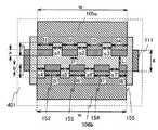
图5A和5B以及图6A和6B示出本示例中的晶体管的详细俯视结构。制造了包括具有不同形状的源电极层和漏电极层的四种晶体管。如图5A所示那样形成了结构A的晶体管400。具体而言,源电极层105a(梳形电极层)的端部和漏电极层105b(梳形电极层)的端部之间的间隔L为3μm,源电极层105a的宽度w(漏电极层105b的宽度w)为50μm,各电极齿形部分的宽度l1、l2、l3、l4、l5、l6、l7、l8为3μm,各电极齿形部分之间的间隔s1、s2、s3、s4、s5、s6为3μm,源电极层105a(漏电极层105b)的各电极齿形部分的长度h(i)为2μm,源电极层105a(漏电极层105b)的各电极齿形部分与栅电极层111的重叠部分的长度a(b)为1.5μm,栅极宽度g为6μm,各电极齿形部分的端部彼此相对的长度P为3μm。5A and 5B and FIGS. 6A and 6B show the detailed top structure of the transistor in this example. Four types of transistors including source and drain electrode layers having different shapes were fabricated. A
如图5B所示那样形成了结构B的晶体管401。具体而言,源电极层105a(梳形电极层)的端部和漏电极层106b(梳形电极层)的端部之间的间隔L为3μm,源电极层105a的宽度w(漏电极层106b的宽度w)为50μm,各电极齿形部分的宽度l1、l2、l3、l4、l5’、l6’、l7’为3μm,l8’为1.5μm,各电极齿形部分之间的间隔s1、s2、s3、s5’、s6’、s7’为3μm,s4’为1.5μm,源电极层105a(漏电极层106b)的各电极齿形部分的长度h(i’)为2μm,源电极层105a(漏电极层106b)的各电极齿形部分与栅电极层111的重叠部分的长度a(b’)为1.5μm,栅极宽度g为6μm,各电极齿形部分的端部彼此相对的长度P’为1.5μm。A
如图6A所示那样形成了结构C的晶体管402。具体而言,源电极层105a(梳形电极层)的端部和漏电极层107b的边缘之间的间隔L为3μm,源电极层105a的宽度w(漏电极层107b的宽度w)为50μm,各电极齿形部分的宽度l1、l2、l3、l4为3μm,各电极齿形部分之间的间隔s1、s2、s3为3μm,源电极层105a的各电极齿形部分的长度h为2μm,源电极层105a的各电极齿形部分与栅电极层111的重叠部分的长度a为1.5μm,漏电极层107b与栅电极层111的重叠部分的长度b”为1.5μm,栅极宽度g为6μm。A
如图6B所示那样形成了现有结构的晶体管403。具体而言,源电极层107a的边缘和漏电极层107b的边缘之间的间隔L为3μm,源电极层107a的宽度w(漏电极层107b的宽度w)为50μm,源电极层107a(漏电极层107b)与栅电极层111的重叠部分的长度a’(b”)为1.5μm,栅极宽度g为6μm。A
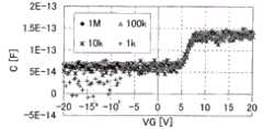
下面,根据实验证明如下事实,即与现有结构的晶体管403相比,设法改变了源电极层和漏电极层的形状的三种晶体管(即晶体管400、401、402)的寄生电容降低。Next, the fact that the parasitic capacitance of three types of transistors (that is,
在下文中示出实验条件。在室温为25℃、衬底温度为25℃、以及在-20至30V(步长0.25V,201步)的范围内使VG变化的条件下,使用具有四个端子的阻抗分析仪(安捷伦科技有限公司制造,4294A),并且将阻抗分析仪的四个端子中的两个端子分别通过GPIB电缆(安捷伦科技有限公司制造)与相应的操纵器连接,来测量在各晶体管的源电极层(漏电极层)与栅电极层的重叠部分产生的寄生电容C。在将探针接触于源电极层和漏电极层中的一方并将源电极层和漏电极层的另一方处于浮动状态的条件下进行测量。在测量之前进行定标,而且每当改变频率时进行定标。在进行该定标时,使操纵器的端子都成为GND。通过使测量频率f以1MHz、100kHz、10kHz、1kHz的四个不同条件发生变化来进行测量。Experimental conditions are shown below. Using an impedance analyzer with four terminals (Agilent Technologies Co., Ltd., 4294A), and two of the four terminals of the impedance analyzer are respectively connected to the corresponding manipulator through the GPIB cable (manufactured by Agilent Technologies Co., Ltd.) to measure the source electrode layer (leakage current) of each transistor electrode layer) and the parasitic capacitance C generated by the overlapping part of the gate electrode layer. The measurement was performed under the condition that the probe was brought into contact with one of the source electrode layer and the drain electrode layer, and the other of the source electrode layer and the drain electrode layer was in a floating state. Calibration is performed before the measurement and whenever the frequency is changed. When performing this calibration, all terminals of the manipulator are set to GND. The measurement was performed by changing the measurement frequency f under four different conditions of 1 MHz, 100 kHz, 10 kHz, and 1 kHz.
图7A至7D表示晶体管的电容特性,其通过实际测量在各晶体管的源电极层(漏电极层)与栅电极层的重叠部分产生的寄生电容C而获得。图7A表示结构A的晶体管400的电容特性,图7B表示结构B的晶体管401的电容特性,图7C表示结构C的晶体管402的电容特性,图7D表示现有结构的晶体管403的电容特性。7A to 7D show capacitance characteristics of transistors obtained by actually measuring a parasitic capacitance C generated at an overlapping portion of a source electrode layer (drain electrode layer) and a gate electrode layer of each transistor. 7A shows the capacitance characteristics of the
可以确认到图7A至7C的每个的寄生电容C低于图7D的寄生电容C。例如,当在频率为1MHz且VG为-20V的条件下测量时,晶体管400的寄生电容C为5.50×10⁻¹⁴F;晶体管401的寄生电容C为5.41×10⁻¹⁴F;晶体管402的寄生电容C为6.74×10⁻¹⁴F;现有结构的晶体管403的寄生电容C为9.63×10⁻¹⁴F。此外,当在频率为1MHz且VG为0V的条件下测量时:晶体管400的寄生电容C为5.54×10⁻¹⁴F;晶体管401的寄生电容C为5.57×10⁻¹⁴F;晶体管402的寄生电容C为6.81×10⁻¹⁴F;现有结构的晶体管403的寄生电容C为9.61×10⁻¹⁴F。It can be confirmed that the parasitic capacitance C of each of FIGS. 7A to 7C is lower than that of FIG. 7D . For example, when the frequency is 1MHz and VG is -20V, the parasitic capacitance C of the
由此可以确认到的是:晶体管400及晶体管401的每一个的源电极层(漏电极层)与栅电极层的重叠部分的面积大约是现有结构的晶体管403的源电极层(漏电极层)与栅电极层的重叠部分的面积的1/2,晶体管402的源电极层(漏电极层)与栅电极层的重叠部分的面积大约是现有结构的晶体管403的源电极层(漏电极层)与栅电极层的重叠部分的面积的3/4,并且,同样地,晶体管400及晶体管401的每一个的寄生电容C大约是现有结构的晶体管403的寄生电容C的1/2,晶体管402的寄生电容C大约是现有结构的晶体管403的寄生电容C的3/4。From this, it can be confirmed that the area of the overlapping portion of the source electrode layer (drain electrode layer) and the gate electrode layer of each of the
从而可以确认到,通过减少源电极层(漏电极层)与栅电极层的重叠部分的面积,可以降低寄生电容。此外,可以确认到,源电极层(漏电极层)和栅电极层的重叠部分的面积与在重叠部分产生的寄生电容是大致成比例的关系。Accordingly, it was confirmed that the parasitic capacitance can be reduced by reducing the area of the overlapping portion of the source electrode layer (drain electrode layer) and the gate electrode layer. In addition, it was confirmed that the area of the overlapping portion of the source electrode layer (drain electrode layer) and the gate electrode layer is approximately proportional to the parasitic capacitance generated in the overlapping portion.
在下文中,根据实验证明现有结构的晶体管403的通态电流与设法改变了源电极层以及漏电极层的形状的三种晶体管(即晶体管400、401、402)的每一个的通态电流大致相同。In the following, it is proved experimentally that the on-state current of the
在下文中示出实验条件。在室温为25℃、衬底温度为25℃、在-20至20V(步长0.2V,201步)的范围中使VG变化、以及VDS为1V的条件下,使用半自动探针(4155B)测量各晶体管的通态电流ID(ID是流在源电极层和漏电极层之间的电流)。Experimental conditions are shown below. Measured with a semi-automatic probe (4155B) at room temperature of 25°C, substrate temperature of 25°C, VG varied in the range of -20 to 20V (0.2V step, 201 steps), and VDS of 1V The on-state current ID of each transistor (ID is the current flowing between the source electrode layer and the drain electrode layer).
图8A和8B各表示根据实际上测量的各晶体管的通态电流获得的晶体管的电流特性。图8A是将图8B的y轴换算成对数标度而得到的图。在图8B中,(1)表示结构A的晶体管400的电流特性,(2)表示结构B的晶体管401的电流特性,(3)表示结构C的晶体管402的电流特性,(4)表示现有结构的晶体管403的电流特性。8A and 8B each represent current characteristics of transistors obtained from actually measured on-state currents of respective transistors. FIG. 8A is a graph obtained by converting the y-axis of FIG. 8B into a logarithmic scale. In FIG. 8B , (1) shows the current characteristics of the
从图8A和8B可确认到,现有结构的晶体管403的通态电流与设法改变了源电极层及漏电极层的形状的三种晶体管(即晶体管400、401、402)的每一个的通态电流大致相同。例如,当在VG为20V的条件下进行测量时:晶体管400的通态电流ID(1)为10.1×10⁻⁵A,晶体管401的通态电流ID(2)为9.69×10⁻⁵A,晶体管402的通态电流ID(3)为11.0×10⁻⁵A,现有结构的晶体管403的通态电流ID(4)为13.35×10⁻⁵A。From FIGS. 8A and 8B, it can be confirmed that the on-state current of the
据此,可以确认到,当减少源电极层(漏电极层)与栅电极层的重叠部分的面积时,虽然通态电流也随着该面积的减少而稍微降低,但其减少率仅为几%左右。From this, it can be confirmed that when the area of the overlapping portion of the source electrode layer (drain electrode layer) and the gate electrode layer is reduced, the on-state current also slightly decreases with the reduction of the area, but the reduction rate is only several %about.
这说明在晶体管400、401、402中可以以足够补偿因为降低寄生电容而降低的线性电流的量,产生以围绕各电极齿形部分的周围的方式流过的曲线电流。即,说明通过将源(漏)电极层的形状从矩形改变为梳形,即使沟道形成区的宽度减少,也可以保持通态电流不变。也就是说,可以确认,晶体管400、401、402、以及现有结构的晶体管403的通态电流的每一个都可认为只依赖于沟道形成区的长度。This means that in the
因此,可以确认到,在设法改变了源电极层和漏电极层的形状的晶体管中,即使降低在源电极层(漏电极层)与栅电极层的重叠部分产生的寄生电容,也可以大致保持通态电流。Therefore, it was confirmed that in a transistor in which the shape of the source electrode layer and the drain electrode layer were changed, even if the parasitic capacitance generated in the overlapping portion of the source electrode layer (drain electrode layer) and the gate electrode layer was reduced, the on-state current.
本申请基于2010年4月7日向日本专利局提交的日本专利申请序列号2010-088634,并将其全部内容并入本文作为参考。This application is based on Japanese Patent Application Serial No. 2010-088634 filed with the Japan Patent Office on April 7, 2010, the entire contents of which are incorporated herein by reference.
Claims (33)
Translated fromChineseApplications Claiming Priority (3)
| Application Number | Priority Date | Filing Date | Title |
|---|---|---|---|
| JP2010088634 | 2010-04-07 | ||
| JP2010-088634 | 2010-04-07 | ||
| PCT/JP2011/056489WO2011125453A1 (en) | 2010-04-07 | 2011-03-11 | Transistor |
Publications (2)
| Publication Number | Publication Date |
|---|---|
| CN102918650Atrue CN102918650A (en) | 2013-02-06 |
| CN102918650B CN102918650B (en) | 2017-03-22 |
Family
ID=44760285
Family Applications (1)
| Application Number | Title | Priority Date | Filing Date |
|---|---|---|---|
| CN201180028292.4AExpired - Fee RelatedCN102918650B (en) | 2010-04-07 | 2011-03-11 | Transistor |
Country Status (6)
| Country | Link |
|---|---|
| US (1) | US9401407B2 (en) |
| JP (2) | JP5806834B2 (en) |
| KR (1) | KR101810592B1 (en) |
| CN (1) | CN102918650B (en) |
| TW (1) | TWI565061B (en) |
| WO (1) | WO2011125453A1 (en) |
Cited By (3)
| Publication number | Priority date | Publication date | Assignee | Title |
|---|---|---|---|---|
| WO2017206660A1 (en)* | 2016-05-31 | 2017-12-07 | 京东方科技集团股份有限公司 | Thin film transistor, array substrate, display panel, and display device |
| CN109166911A (en)* | 2018-07-25 | 2019-01-08 | 深圳市华星光电技术有限公司 | Thin film transistor (TFT), array substrate and display device |
| CN115132832A (en)* | 2022-07-29 | 2022-09-30 | 京东方科技集团股份有限公司 | Thin film transistor, array substrate, display panel and display device |
Families Citing this family (11)
| Publication number | Priority date | Publication date | Assignee | Title |
|---|---|---|---|---|
| US9097947B2 (en) | 2011-05-12 | 2015-08-04 | Semiconductor Energy Laboratory Co., Ltd. | Display device and manufacturing method thereof |
| EP2786404A4 (en) | 2011-12-02 | 2015-07-15 | Semiconductor Energy Lab | SEMICONDUCTOR DEVICE AND METHOD FOR MANUFACTURING THE SAME |
| JP6285150B2 (en) | 2012-11-16 | 2018-02-28 | 株式会社半導体エネルギー研究所 | Semiconductor device |
| US9153672B2 (en)* | 2012-12-21 | 2015-10-06 | Taiwan Semiconductor Manufacturing Co., Ltd. | Vertical BJT for high density memory |
| US9853154B2 (en) | 2014-01-24 | 2017-12-26 | Taiwan Semiconductor Manufacturing Company Ltd. | Embedded source or drain region of transistor with downward tapered region under facet region |
| US10164107B2 (en) | 2014-01-24 | 2018-12-25 | Taiwan Semiconductor Manufacturing Company Ltd. | Embedded source or drain region of transistor with laterally extended portion |
| JP6546400B2 (en)* | 2015-02-05 | 2019-07-17 | 株式会社ジャパンディスプレイ | Display device |
| KR102330497B1 (en) | 2015-06-02 | 2021-11-24 | 삼성디스플레이 주식회사 | Gate driving cirucit and display device having the same |
| US20180356660A1 (en)* | 2015-12-09 | 2018-12-13 | Sharp Kabushiki Kaisha | Active matrix substrate and liquid crystal display panel provided with same |
| KR102576999B1 (en)* | 2016-07-05 | 2023-09-12 | 삼성디스플레이 주식회사 | Liquid-crystal display |
| WO2018190396A1 (en)* | 2017-04-13 | 2018-10-18 | シャープ株式会社 | Active matrix substrate |
Citations (4)
| Publication number | Priority date | Publication date | Assignee | Title |
|---|---|---|---|---|
| JPH05183165A (en)* | 1991-12-27 | 1993-07-23 | Kanegafuchi Chem Ind Co Ltd | Thin film transistor |
| US20080038882A1 (en)* | 2006-08-09 | 2008-02-14 | Kazushige Takechi | Thin-film device and method of fabricating the same |
| US20080157136A1 (en)* | 2006-12-27 | 2008-07-03 | Casio Computer Co., Ltd. | Thin-film transistor type photosensor |
| US20090283762A1 (en)* | 2008-05-16 | 2009-11-19 | Semiconductor Energy Laboratory Co., Ltd. | Semiconductor device and manufacturing method of the same |
Family Cites Families (122)
| Publication number | Priority date | Publication date | Assignee | Title |
|---|---|---|---|---|
| DE2654001C2 (en) | 1976-11-27 | 1986-02-06 | Harald 5210 Troisdorf Feuerherm | Device for producing hollow bodies made of thermoplastic material |
| JPS6054171U (en)* | 1983-09-20 | 1985-04-16 | 三洋電機株式会社 | liquid crystal display device |
| JPS60198861A (en) | 1984-03-23 | 1985-10-08 | Fujitsu Ltd | Thin film transistor |
| JPS62287666A (en) | 1986-06-03 | 1987-12-14 | ゼネラル・エレクトリツク・カンパニイ | Thin film field effect transistor allowing discrepancy of electrode position |
| JPH0244256B2 (en) | 1987-01-28 | 1990-10-03 | Kagaku Gijutsucho Mukizaishitsu Kenkyushocho | INGAZN2O5DESHIMESARERUROTSUHOSHOKEINOSOJOKOZOOJUSURUKAGOBUTSUOYOBISONOSEIZOHO |
| JPH0244258B2 (en) | 1987-02-24 | 1990-10-03 | Kagaku Gijutsucho Mukizaishitsu Kenkyushocho | INGAZN3O6DESHIMESARERUROTSUHOSHOKEINOSOJOKOZOOJUSURUKAGOBUTSUOYOBISONOSEIZOHO |
| JPH0244260B2 (en) | 1987-02-24 | 1990-10-03 | Kagaku Gijutsucho Mukizaishitsu Kenkyushocho | INGAZN5O8DESHIMESARERUROTSUHOSHOKEINOSOJOKOZOOJUSURUKAGOBUTSUOYOBISONOSEIZOHO |
| JPS63210023A (en) | 1987-02-24 | 1988-08-31 | Natl Inst For Res In Inorg Mater | Compound having a hexagonal layered structure represented by InGaZn↓4O↓7 and its manufacturing method |
| JPH0244262B2 (en) | 1987-02-27 | 1990-10-03 | Kagaku Gijutsucho Mukizaishitsu Kenkyushocho | INGAZN6O9DESHIMESARERUROTSUHOSHOKEINOSOJOKOZOOJUSURUKAGOBUTSUOYOBISONOSEIZOHO |
| JPH0244263B2 (en) | 1987-04-22 | 1990-10-03 | Kagaku Gijutsucho Mukizaishitsu Kenkyushocho | INGAZN7O10DESHIMESARERUROTSUHOSHOKEINOSOJOKOZOOJUSURUKAGOBUTSUOYOBISONOSEIZOHO |
| JPH0258030A (en)* | 1988-08-24 | 1990-02-27 | Hitachi Ltd | liquid crystal display device |
| JPH02275672A (en)* | 1989-03-30 | 1990-11-09 | Nippon Steel Corp | thin film transistor |
| US5302987A (en)* | 1991-05-15 | 1994-04-12 | Sharp Kabushiki Kaisha | Active matrix substrate including connecting electrode with extended portion |
| JPH04360583A (en) | 1991-06-07 | 1992-12-14 | Nippon Steel Corp | thin film transistor |
| JPH05251705A (en) | 1992-03-04 | 1993-09-28 | Fuji Xerox Co Ltd | Thin-film transistor |
| JPH0815728A (en) | 1994-06-30 | 1996-01-19 | Sanyo Electric Co Ltd | Liquid crystal display device |
| JP3479375B2 (en) | 1995-03-27 | 2003-12-15 | 科学技術振興事業団 | Metal oxide semiconductor device in which a pn junction is formed with a thin film transistor made of a metal oxide semiconductor such as cuprous oxide, and methods for manufacturing the same |
| KR100394896B1 (en) | 1995-08-03 | 2003-11-28 | 코닌클리케 필립스 일렉트로닉스 엔.브이. | A semiconductor device including a transparent switching element |
| JP3625598B2 (en) | 1995-12-30 | 2005-03-02 | 三星電子株式会社 | Manufacturing method of liquid crystal display device |
| JPH11177102A (en) | 1997-12-08 | 1999-07-02 | Semiconductor Energy Lab Co Ltd | Semiconductor device and manufacturing method thereof |
| JP4170454B2 (en) | 1998-07-24 | 2008-10-22 | Hoya株式会社 | Article having transparent conductive oxide thin film and method for producing the same |
| JP2000150861A (en) | 1998-11-16 | 2000-05-30 | Tdk Corp | Oxide thin film |
| JP3276930B2 (en) | 1998-11-17 | 2002-04-22 | 科学技術振興事業団 | Transistor and semiconductor device |
| TW460731B (en) | 1999-09-03 | 2001-10-21 | Ind Tech Res Inst | Electrode structure and production method of wide viewing angle LCD |
| JP2001209070A (en) | 2000-01-27 | 2001-08-03 | Casio Comput Co Ltd | Liquid crystal display device |
| JP2001296553A (en)* | 2000-04-14 | 2001-10-26 | Advanced Display Inc | Display device and method of manufacturing display device |
| US7019457B2 (en) | 2000-08-03 | 2006-03-28 | Semiconductor Energy Laboratory Co., Ltd. | Light emitting device having both electrodes formed on the insulating layer |
| JP4089858B2 (en) | 2000-09-01 | 2008-05-28 | 国立大学法人東北大学 | Semiconductor device |
| KR20020038482A (en) | 2000-11-15 | 2002-05-23 | 모리시타 요이찌 | Thin film transistor array, method for producing the same, and display panel using the same |
| JP3997731B2 (en) | 2001-03-19 | 2007-10-24 | 富士ゼロックス株式会社 | Method for forming a crystalline semiconductor thin film on a substrate |
| JP2002289859A (en) | 2001-03-23 | 2002-10-04 | Minolta Co Ltd | Thin film transistor |
| JP3925839B2 (en) | 2001-09-10 | 2007-06-06 | シャープ株式会社 | Semiconductor memory device and test method thereof |
| JP4090716B2 (en) | 2001-09-10 | 2008-05-28 | 雅司 川崎 | Thin film transistor and matrix display device |
| WO2003040441A1 (en) | 2001-11-05 | 2003-05-15 | Japan Science And Technology Agency | Natural superlattice homologous single crystal thin film, method for preparation thereof, and device using said single crystal thin film |
| JP4164562B2 (en) | 2002-09-11 | 2008-10-15 | 独立行政法人科学技術振興機構 | Transparent thin film field effect transistor using homologous thin film as active layer |
| JP4083486B2 (en) | 2002-02-21 | 2008-04-30 | 独立行政法人科学技術振興機構 | Method for producing LnCuO (S, Se, Te) single crystal thin film |
| CN1445821A (en) | 2002-03-15 | 2003-10-01 | 三洋电机株式会社 | Forming method of ZnO film and ZnO semiconductor layer, semiconductor element and manufacturing method thereof |
| JP3933591B2 (en) | 2002-03-26 | 2007-06-20 | 淳二 城戸 | Organic electroluminescent device |
| KR20030086168A (en)* | 2002-05-03 | 2003-11-07 | 엘지.필립스 엘시디 주식회사 | The organic electro-luminescence device and method for fabricating of the same |
| US7339187B2 (en) | 2002-05-21 | 2008-03-04 | State Of Oregon Acting By And Through The Oregon State Board Of Higher Education On Behalf Of Oregon State University | Transistor structures |
| JP2004022625A (en) | 2002-06-13 | 2004-01-22 | Murata Mfg Co Ltd | Semiconductor device and method of manufacturing the semiconductor device |
| US7105868B2 (en) | 2002-06-24 | 2006-09-12 | Cermet, Inc. | High-electron mobility transistor with zinc oxide |
| US7067843B2 (en) | 2002-10-11 | 2006-06-27 | E. I. Du Pont De Nemours And Company | Transparent oxide semiconductor thin film transistors |
| KR100918180B1 (en)* | 2003-03-04 | 2009-09-22 | 삼성전자주식회사 | Shift register |
| JP4166105B2 (en) | 2003-03-06 | 2008-10-15 | シャープ株式会社 | Semiconductor device and manufacturing method thereof |
| JP2004273732A (en) | 2003-03-07 | 2004-09-30 | Sharp Corp | Active matrix substrate and manufacturing method thereof |
| JP4108633B2 (en) | 2003-06-20 | 2008-06-25 | シャープ株式会社 | THIN FILM TRANSISTOR, MANUFACTURING METHOD THEREOF, AND ELECTRONIC DEVICE |
| US8319219B2 (en) | 2003-07-14 | 2012-11-27 | Semiconductor Energy Laboratory Co., Ltd. | Light-emitting device |
| US7262463B2 (en) | 2003-07-25 | 2007-08-28 | Hewlett-Packard Development Company, L.P. | Transistor including a deposited channel region having a doped portion |
| KR100553935B1 (en)* | 2003-08-20 | 2006-02-24 | 엘지.필립스 엘시디 주식회사 | LCD and its manufacturing method |
| JP2005175248A (en)* | 2003-12-12 | 2005-06-30 | Sanyo Electric Co Ltd | Liquid crystal display of field sequential system |
| US7297977B2 (en) | 2004-03-12 | 2007-11-20 | Hewlett-Packard Development Company, L.P. | Semiconductor device |
| US7145174B2 (en) | 2004-03-12 | 2006-12-05 | Hewlett-Packard Development Company, Lp. | Semiconductor device |
| US7282782B2 (en) | 2004-03-12 | 2007-10-16 | Hewlett-Packard Development Company, L.P. | Combined binary oxide semiconductor device |
| CN1998087B (en) | 2004-03-12 | 2014-12-31 | 独立行政法人科学技术振兴机构 | Amorphous oxide and thin film transistor |
| US7211825B2 (en) | 2004-06-14 | 2007-05-01 | Yi-Chi Shih | Indium oxide-based thin film transistors and circuits |
| JP2006100760A (en) | 2004-09-02 | 2006-04-13 | Casio Comput Co Ltd | Thin film transistor and manufacturing method thereof |
| US7285501B2 (en) | 2004-09-17 | 2007-10-23 | Hewlett-Packard Development Company, L.P. | Method of forming a solution processed device |
| US7298084B2 (en) | 2004-11-02 | 2007-11-20 | 3M Innovative Properties Company | Methods and displays utilizing integrated zinc oxide row and column drivers in conjunction with organic light emitting diodes |
| US7791072B2 (en) | 2004-11-10 | 2010-09-07 | Canon Kabushiki Kaisha | Display |
| US7453065B2 (en) | 2004-11-10 | 2008-11-18 | Canon Kabushiki Kaisha | Sensor and image pickup device |
| EP2453481B1 (en) | 2004-11-10 | 2017-01-11 | Canon Kabushiki Kaisha | Field effect transistor with amorphous oxide |
| US7829444B2 (en) | 2004-11-10 | 2010-11-09 | Canon Kabushiki Kaisha | Field effect transistor manufacturing method |
| US7863611B2 (en) | 2004-11-10 | 2011-01-04 | Canon Kabushiki Kaisha | Integrated circuits utilizing amorphous oxides |
| AU2005302964B2 (en) | 2004-11-10 | 2010-11-04 | Canon Kabushiki Kaisha | Field effect transistor employing an amorphous oxide |
| KR100953596B1 (en) | 2004-11-10 | 2010-04-21 | 캐논 가부시끼가이샤 | Light emitting device |
| US7579224B2 (en) | 2005-01-21 | 2009-08-25 | Semiconductor Energy Laboratory Co., Ltd. | Method for manufacturing a thin film semiconductor device |
| TWI445178B (en) | 2005-01-28 | 2014-07-11 | Semiconductor Energy Lab | Semiconductor device, electronic device, and method of manufacturing semiconductor device |
| TWI505473B (en) | 2005-01-28 | 2015-10-21 | Semiconductor Energy Lab | Semiconductor device, electronic device, and method of manufacturing semiconductor device |
| US7858451B2 (en) | 2005-02-03 | 2010-12-28 | Semiconductor Energy Laboratory Co., Ltd. | Electronic device, semiconductor device and manufacturing method thereof |
| US7948171B2 (en) | 2005-02-18 | 2011-05-24 | Semiconductor Energy Laboratory Co., Ltd. | Light emitting device |
| US20060197092A1 (en) | 2005-03-03 | 2006-09-07 | Randy Hoffman | System and method for forming conductive material on a substrate |
| US8681077B2 (en) | 2005-03-18 | 2014-03-25 | Semiconductor Energy Laboratory Co., Ltd. | Semiconductor device, and display device, driving method and electronic apparatus thereof |
| US7544967B2 (en) | 2005-03-28 | 2009-06-09 | Massachusetts Institute Of Technology | Low voltage flexible organic/transparent transistor for selective gas sensing, photodetecting and CMOS device applications |
| US7645478B2 (en) | 2005-03-31 | 2010-01-12 | 3M Innovative Properties Company | Methods of making displays |
| US8300031B2 (en) | 2005-04-20 | 2012-10-30 | Semiconductor Energy Laboratory Co., Ltd. | Semiconductor device comprising transistor having gate and drain connected through a current-voltage conversion element |
| JP2006344849A (en) | 2005-06-10 | 2006-12-21 | Casio Comput Co Ltd | Thin film transistor |
| US7402506B2 (en) | 2005-06-16 | 2008-07-22 | Eastman Kodak Company | Methods of making thin film transistors comprising zinc-oxide-based semiconductor materials and transistors made thereby |
| US7691666B2 (en) | 2005-06-16 | 2010-04-06 | Eastman Kodak Company | Methods of making thin film transistors comprising zinc-oxide-based semiconductor materials and transistors made thereby |
| US7507618B2 (en) | 2005-06-27 | 2009-03-24 | 3M Innovative Properties Company | Method for making electronic devices using metal oxide nanoparticles |
| KR100711890B1 (en) | 2005-07-28 | 2007-04-25 | 삼성에스디아이 주식회사 | OLED display and manufacturing method thereof |
| JP2007059128A (en) | 2005-08-23 | 2007-03-08 | Canon Inc | Organic EL display device and manufacturing method thereof |
| JP4850457B2 (en) | 2005-09-06 | 2012-01-11 | キヤノン株式会社 | Thin film transistor and thin film diode |
| JP2007073705A (en) | 2005-09-06 | 2007-03-22 | Canon Inc | Oxide semiconductor channel thin film transistor and method for manufacturing the same |
| JP5116225B2 (en) | 2005-09-06 | 2013-01-09 | キヤノン株式会社 | Manufacturing method of oxide semiconductor device |
| JP4280736B2 (en) | 2005-09-06 | 2009-06-17 | キヤノン株式会社 | Semiconductor element |
| EP1770788A3 (en) | 2005-09-29 | 2011-09-21 | Semiconductor Energy Laboratory Co., Ltd. | Semiconductor device having oxide semiconductor layer and manufacturing method thereof |
| JP5037808B2 (en) | 2005-10-20 | 2012-10-03 | キヤノン株式会社 | Field effect transistor using amorphous oxide, and display device using the transistor |
| CN101577231B (en) | 2005-11-15 | 2013-01-02 | 株式会社半导体能源研究所 | Semiconductor device and method of manufacturing the same |
| KR20070059559A (en) | 2005-12-07 | 2007-06-12 | 삼성전자주식회사 | Display device and manufacturing method thereof |
| US8212238B2 (en) | 2005-12-27 | 2012-07-03 | Semiconductor Energy Laboratory Co., Ltd. | Semiconductor device and manufacturing method thereof |
| TWI292281B (en) | 2005-12-29 | 2008-01-01 | Ind Tech Res Inst | Pixel structure of active organic light emitting diode and method of fabricating the same |
| US7867636B2 (en) | 2006-01-11 | 2011-01-11 | Murata Manufacturing Co., Ltd. | Transparent conductive film and method for manufacturing the same |
| JP4977478B2 (en) | 2006-01-21 | 2012-07-18 | 三星電子株式会社 | ZnO film and method of manufacturing TFT using the same |
| US7576394B2 (en) | 2006-02-02 | 2009-08-18 | Kochi Industrial Promotion Center | Thin film transistor including low resistance conductive thin films and manufacturing method thereof |
| US7977169B2 (en) | 2006-02-15 | 2011-07-12 | Kochi Industrial Promotion Center | Semiconductor device including active layer made of zinc oxide with controlled orientations and manufacturing method thereof |
| KR20070101595A (en) | 2006-04-11 | 2007-10-17 | 삼성전자주식회사 | ZnO TFT |
| US20070252928A1 (en) | 2006-04-28 | 2007-11-01 | Toppan Printing Co., Ltd. | Structure, transmission type liquid crystal display, reflection type display and manufacturing method thereof |
| JP2007310180A (en) | 2006-05-19 | 2007-11-29 | Mitsubishi Electric Corp | Liquid crystal display device and defective pixel repair method thereof |
| JP5028033B2 (en) | 2006-06-13 | 2012-09-19 | キヤノン株式会社 | Oxide semiconductor film dry etching method |
| JP4999400B2 (en) | 2006-08-09 | 2012-08-15 | キヤノン株式会社 | Oxide semiconductor film dry etching method |
| JP4332545B2 (en) | 2006-09-15 | 2009-09-16 | キヤノン株式会社 | Field effect transistor and manufacturing method thereof |
| JP5164357B2 (en) | 2006-09-27 | 2013-03-21 | キヤノン株式会社 | Semiconductor device and manufacturing method of semiconductor device |
| JP4274219B2 (en) | 2006-09-27 | 2009-06-03 | セイコーエプソン株式会社 | Electronic devices, organic electroluminescence devices, organic thin film semiconductor devices |
| US7622371B2 (en) | 2006-10-10 | 2009-11-24 | Hewlett-Packard Development Company, L.P. | Fused nanocrystal thin film semiconductor and method |
| US7772021B2 (en) | 2006-11-29 | 2010-08-10 | Samsung Electronics Co., Ltd. | Flat panel displays comprising a thin-film transistor having a semiconductive oxide in its channel and methods of fabricating the same for use in flat panel displays |
| JP2008140684A (en) | 2006-12-04 | 2008-06-19 | Toppan Printing Co Ltd | Color EL display and manufacturing method thereof |
| KR101303578B1 (en) | 2007-01-05 | 2013-09-09 | 삼성전자주식회사 | Etching method of thin film |
| US8207063B2 (en) | 2007-01-26 | 2012-06-26 | Eastman Kodak Company | Process for atomic layer deposition |
| KR100851215B1 (en) | 2007-03-14 | 2008-08-07 | 삼성에스디아이 주식회사 | Thin film transistor and organic light emitting display device using same |
| US7795613B2 (en) | 2007-04-17 | 2010-09-14 | Toppan Printing Co., Ltd. | Structure with transistor |
| KR101325053B1 (en) | 2007-04-18 | 2013-11-05 | 삼성디스플레이 주식회사 | Thin film transistor substrate and manufacturing method thereof |
| KR20080094300A (en) | 2007-04-19 | 2008-10-23 | 삼성전자주식회사 | Thin film transistors and methods of manufacturing the same and flat panel displays comprising thin film transistors |
| KR101334181B1 (en) | 2007-04-20 | 2013-11-28 | 삼성전자주식회사 | Thin Film Transistor having selectively crystallized channel layer and method of manufacturing the same |
| CN101663762B (en) | 2007-04-25 | 2011-09-21 | 佳能株式会社 | Oxynitride semiconductor |
| KR101345376B1 (en) | 2007-05-29 | 2013-12-24 | 삼성전자주식회사 | Fabrication method of ZnO family Thin film transistor |
| US8202365B2 (en) | 2007-12-17 | 2012-06-19 | Fujifilm Corporation | Process for producing oriented inorganic crystalline film, and semiconductor device using the oriented inorganic crystalline film |
| JP2010003723A (en)* | 2008-06-18 | 2010-01-07 | Toppan Printing Co Ltd | Thin-film transistor, thin-film transistor array and image display |
| KR100958006B1 (en) | 2008-06-18 | 2010-05-17 | 삼성모바일디스플레이주식회사 | Thin film transistor, its manufacturing method, and flat panel display device comprising thin film transistor |
| JP5584960B2 (en) | 2008-07-03 | 2014-09-10 | ソニー株式会社 | Thin film transistor and display device |
| JP4623179B2 (en) | 2008-09-18 | 2011-02-02 | ソニー株式会社 | Thin film transistor and manufacturing method thereof |
| JP5451280B2 (en) | 2008-10-09 | 2014-03-26 | キヤノン株式会社 | Wurtzite crystal growth substrate, manufacturing method thereof, and semiconductor device |
- 2011
- 2011-03-11WOPCT/JP2011/056489patent/WO2011125453A1/enactiveApplication Filing
- 2011-03-11CNCN201180028292.4Apatent/CN102918650B/ennot_activeExpired - Fee Related
- 2011-03-11KRKR1020127029249Apatent/KR101810592B1/enactiveActive
- 2011-03-29TWTW100110790Apatent/TWI565061B/ennot_activeIP Right Cessation
- 2011-03-31USUS13/076,806patent/US9401407B2/ennot_activeExpired - Fee Related
- 2011-04-07JPJP2011085473Apatent/JP5806834B2/enactiveActive
- 2015
- 2015-09-07JPJP2015175756Apatent/JP6124966B2/ennot_activeExpired - Fee Related
Patent Citations (4)
| Publication number | Priority date | Publication date | Assignee | Title |
|---|---|---|---|---|
| JPH05183165A (en)* | 1991-12-27 | 1993-07-23 | Kanegafuchi Chem Ind Co Ltd | Thin film transistor |
| US20080038882A1 (en)* | 2006-08-09 | 2008-02-14 | Kazushige Takechi | Thin-film device and method of fabricating the same |
| US20080157136A1 (en)* | 2006-12-27 | 2008-07-03 | Casio Computer Co., Ltd. | Thin-film transistor type photosensor |
| US20090283762A1 (en)* | 2008-05-16 | 2009-11-19 | Semiconductor Energy Laboratory Co., Ltd. | Semiconductor device and manufacturing method of the same |
Cited By (4)
| Publication number | Priority date | Publication date | Assignee | Title |
|---|---|---|---|---|
| WO2017206660A1 (en)* | 2016-05-31 | 2017-12-07 | 京东方科技集团股份有限公司 | Thin film transistor, array substrate, display panel, and display device |
| US11474386B2 (en) | 2016-05-31 | 2022-10-18 | Boe Technology Group Co., Ltd. | Thin-film transistor, array substrate, display panel and display device |
| CN109166911A (en)* | 2018-07-25 | 2019-01-08 | 深圳市华星光电技术有限公司 | Thin film transistor (TFT), array substrate and display device |
| CN115132832A (en)* | 2022-07-29 | 2022-09-30 | 京东方科技集团股份有限公司 | Thin film transistor, array substrate, display panel and display device |
Also Published As
| Publication number | Publication date |
|---|---|
| US20110248266A1 (en) | 2011-10-13 |
| JP2011233882A (en) | 2011-11-17 |
| KR101810592B1 (en) | 2017-12-20 |
| CN102918650B (en) | 2017-03-22 |
| JP2016012731A (en) | 2016-01-21 |
| US9401407B2 (en) | 2016-07-26 |
| TW201203550A (en) | 2012-01-16 |
| WO2011125453A1 (en) | 2011-10-13 |
| JP5806834B2 (en) | 2015-11-10 |
| KR20130038856A (en) | 2013-04-18 |
| JP6124966B2 (en) | 2017-05-10 |
| TWI565061B (en) | 2017-01-01 |
Similar Documents
| Publication | Publication Date | Title |
|---|---|---|
| CN102918650B (en) | Transistor | |
| JP7194791B2 (en) | semiconductor equipment | |
| JP6982638B2 (en) | Semiconductor device | |
| JP6971347B2 (en) | Semiconductor device | |
| JP7046293B2 (en) | Semiconductor device | |
| JP6792017B2 (en) | Manufacturing method of semiconductor device | |
| JP6298186B2 (en) | Semiconductor device | |
| JP5839554B2 (en) | Semiconductor device | |
| JP5955538B2 (en) | Semiconductor device | |
| CN102484139B (en) | Oxide semiconductor layer and semiconductor device | |
| CN103137701B (en) | Transistor and semiconductor device | |
| JP6421221B2 (en) | Semiconductor device | |
| JPWO2011132418A1 (en) | Deposition method | |
| TWI514261B (en) | Divider circuit |
Legal Events
| Date | Code | Title | Description |
|---|---|---|---|
| C06 | Publication | ||
| PB01 | Publication | ||
| C10 | Entry into substantive examination | ||
| SE01 | Entry into force of request for substantive examination | ||
| C14 | Grant of patent or utility model | ||
| GR01 | Patent grant | ||
| CF01 | Termination of patent right due to non-payment of annual fee | Granted publication date:20170322 Termination date:20210311 | |
| CF01 | Termination of patent right due to non-payment of annual fee |