CN102914372A - Infrared detecting element and electronic device - Google Patents
Infrared detecting element and electronic deviceDownload PDFInfo
- Publication number
- CN102914372A CN102914372ACN201210273610XACN201210273610ACN102914372ACN 102914372 ACN102914372 ACN 102914372ACN 201210273610X ACN201210273610X ACN 201210273610XACN 201210273610 ACN201210273610 ACN 201210273610ACN 102914372 ACN102914372 ACN 102914372A
- Authority
- CN
- China
- Prior art keywords
- infrared detection
- substrate
- adhesive
- detection element
- infrared
- Prior art date
- Legal status (The legal status is an assumption and is not a legal conclusion. Google has not performed a legal analysis and makes no representation as to the accuracy of the status listed.)
- Pending
Links
Images


Classifications
- G—PHYSICS
- G01—MEASURING; TESTING
- G01J—MEASUREMENT OF INTENSITY, VELOCITY, SPECTRAL CONTENT, POLARISATION, PHASE OR PULSE CHARACTERISTICS OF INFRARED, VISIBLE OR ULTRAVIOLET LIGHT; COLORIMETRY; RADIATION PYROMETRY
- G01J5/00—Radiation pyrometry, e.g. infrared or optical thermometry
- G01J5/02—Constructional details
- G01J5/0225—Shape of the cavity itself or of elements contained in or suspended over the cavity
- G—PHYSICS
- G01—MEASURING; TESTING
- G01J—MEASUREMENT OF INTENSITY, VELOCITY, SPECTRAL CONTENT, POLARISATION, PHASE OR PULSE CHARACTERISTICS OF INFRARED, VISIBLE OR ULTRAVIOLET LIGHT; COLORIMETRY; RADIATION PYROMETRY
- G01J5/00—Radiation pyrometry, e.g. infrared or optical thermometry
- G01J5/02—Constructional details
- G01J5/0205—Mechanical elements; Supports for optical elements
- G—PHYSICS
- G01—MEASURING; TESTING
- G01J—MEASUREMENT OF INTENSITY, VELOCITY, SPECTRAL CONTENT, POLARISATION, PHASE OR PULSE CHARACTERISTICS OF INFRARED, VISIBLE OR ULTRAVIOLET LIGHT; COLORIMETRY; RADIATION PYROMETRY
- G01J5/00—Radiation pyrometry, e.g. infrared or optical thermometry
- G01J5/10—Radiation pyrometry, e.g. infrared or optical thermometry using electric radiation detectors
- G01J5/34—Radiation pyrometry, e.g. infrared or optical thermometry using electric radiation detectors using capacitors, e.g. pyroelectric capacitors
- H—ELECTRICITY
- H10—SEMICONDUCTOR DEVICES; ELECTRIC SOLID-STATE DEVICES NOT OTHERWISE PROVIDED FOR
- H10F—INORGANIC SEMICONDUCTOR DEVICES SENSITIVE TO INFRARED RADIATION, LIGHT, ELECTROMAGNETIC RADIATION OF SHORTER WAVELENGTH OR CORPUSCULAR RADIATION
- H10F77/00—Constructional details of devices covered by this subclass
- H10F77/50—Encapsulations or containers
- G—PHYSICS
- G01—MEASURING; TESTING
- G01J—MEASUREMENT OF INTENSITY, VELOCITY, SPECTRAL CONTENT, POLARISATION, PHASE OR PULSE CHARACTERISTICS OF INFRARED, VISIBLE OR ULTRAVIOLET LIGHT; COLORIMETRY; RADIATION PYROMETRY
- G01J5/00—Radiation pyrometry, e.g. infrared or optical thermometry
- G01J2005/0077—Imaging
- G—PHYSICS
- G01—MEASURING; TESTING
- G01J—MEASUREMENT OF INTENSITY, VELOCITY, SPECTRAL CONTENT, POLARISATION, PHASE OR PULSE CHARACTERISTICS OF INFRARED, VISIBLE OR ULTRAVIOLET LIGHT; COLORIMETRY; RADIATION PYROMETRY
- G01J5/00—Radiation pyrometry, e.g. infrared or optical thermometry
- G01J5/10—Radiation pyrometry, e.g. infrared or optical thermometry using electric radiation detectors
- G01J2005/106—Arrays
- G—PHYSICS
- G01—MEASURING; TESTING
- G01J—MEASUREMENT OF INTENSITY, VELOCITY, SPECTRAL CONTENT, POLARISATION, PHASE OR PULSE CHARACTERISTICS OF INFRARED, VISIBLE OR ULTRAVIOLET LIGHT; COLORIMETRY; RADIATION PYROMETRY
- G01J5/00—Radiation pyrometry, e.g. infrared or optical thermometry
- G01J5/10—Radiation pyrometry, e.g. infrared or optical thermometry using electric radiation detectors
- G01J5/20—Radiation pyrometry, e.g. infrared or optical thermometry using electric radiation detectors using resistors, thermistors or semiconductors sensitive to radiation, e.g. photoconductive devices
- G01J2005/202—Arrays
- G—PHYSICS
- G01—MEASURING; TESTING
- G01J—MEASUREMENT OF INTENSITY, VELOCITY, SPECTRAL CONTENT, POLARISATION, PHASE OR PULSE CHARACTERISTICS OF INFRARED, VISIBLE OR ULTRAVIOLET LIGHT; COLORIMETRY; RADIATION PYROMETRY
- G01J5/00—Radiation pyrometry, e.g. infrared or optical thermometry
- G01J5/10—Radiation pyrometry, e.g. infrared or optical thermometry using electric radiation detectors
- G01J5/34—Radiation pyrometry, e.g. infrared or optical thermometry using electric radiation detectors using capacitors, e.g. pyroelectric capacitors
- G01J2005/345—Arrays
- G—PHYSICS
- G01—MEASURING; TESTING
- G01J—MEASUREMENT OF INTENSITY, VELOCITY, SPECTRAL CONTENT, POLARISATION, PHASE OR PULSE CHARACTERISTICS OF INFRARED, VISIBLE OR ULTRAVIOLET LIGHT; COLORIMETRY; RADIATION PYROMETRY
- G01J5/00—Radiation pyrometry, e.g. infrared or optical thermometry
- G01J5/0003—Radiation pyrometry, e.g. infrared or optical thermometry for sensing the radiant heat transfer of samples, e.g. emittance meter
- G—PHYSICS
- G01—MEASURING; TESTING
- G01J—MEASUREMENT OF INTENSITY, VELOCITY, SPECTRAL CONTENT, POLARISATION, PHASE OR PULSE CHARACTERISTICS OF INFRARED, VISIBLE OR ULTRAVIOLET LIGHT; COLORIMETRY; RADIATION PYROMETRY
- G01J5/00—Radiation pyrometry, e.g. infrared or optical thermometry
- G01J5/0022—Radiation pyrometry, e.g. infrared or optical thermometry for sensing the radiation of moving bodies
- G01J5/0025—Living bodies
- G—PHYSICS
- G01—MEASURING; TESTING
- G01J—MEASUREMENT OF INTENSITY, VELOCITY, SPECTRAL CONTENT, POLARISATION, PHASE OR PULSE CHARACTERISTICS OF INFRARED, VISIBLE OR ULTRAVIOLET LIGHT; COLORIMETRY; RADIATION PYROMETRY
- G01J5/00—Radiation pyrometry, e.g. infrared or optical thermometry
- G01J5/02—Constructional details
- G01J5/0225—Shape of the cavity itself or of elements contained in or suspended over the cavity
- G01J5/023—Particular leg structure or construction or shape; Nanotubes
- G—PHYSICS
- G01—MEASURING; TESTING
- G01J—MEASUREMENT OF INTENSITY, VELOCITY, SPECTRAL CONTENT, POLARISATION, PHASE OR PULSE CHARACTERISTICS OF INFRARED, VISIBLE OR ULTRAVIOLET LIGHT; COLORIMETRY; RADIATION PYROMETRY
- G01J5/00—Radiation pyrometry, e.g. infrared or optical thermometry
- G01J5/02—Constructional details
- G01J5/0225—Shape of the cavity itself or of elements contained in or suspended over the cavity
- G01J5/024—Special manufacturing steps or sacrificial layers or layer structures
- G—PHYSICS
- G01—MEASURING; TESTING
- G01J—MEASUREMENT OF INTENSITY, VELOCITY, SPECTRAL CONTENT, POLARISATION, PHASE OR PULSE CHARACTERISTICS OF INFRARED, VISIBLE OR ULTRAVIOLET LIGHT; COLORIMETRY; RADIATION PYROMETRY
- G01J5/00—Radiation pyrometry, e.g. infrared or optical thermometry
- G01J5/10—Radiation pyrometry, e.g. infrared or optical thermometry using electric radiation detectors
- G—PHYSICS
- G01—MEASURING; TESTING
- G01N—INVESTIGATING OR ANALYSING MATERIALS BY DETERMINING THEIR CHEMICAL OR PHYSICAL PROPERTIES
- G01N21/00—Investigating or analysing materials by the use of optical means, i.e. using sub-millimetre waves, infrared, visible or ultraviolet light
- G01N21/01—Arrangements or apparatus for facilitating the optical investigation
- G01N2021/0106—General arrangement of respective parts
- G—PHYSICS
- G01—MEASURING; TESTING
- G01N—INVESTIGATING OR ANALYSING MATERIALS BY DETERMINING THEIR CHEMICAL OR PHYSICAL PROPERTIES
- G01N21/00—Investigating or analysing materials by the use of optical means, i.e. using sub-millimetre waves, infrared, visible or ultraviolet light
- G01N21/17—Systems in which incident light is modified in accordance with the properties of the material investigated
- G—PHYSICS
- G01—MEASURING; TESTING
- G01N—INVESTIGATING OR ANALYSING MATERIALS BY DETERMINING THEIR CHEMICAL OR PHYSICAL PROPERTIES
- G01N21/00—Investigating or analysing materials by the use of optical means, i.e. using sub-millimetre waves, infrared, visible or ultraviolet light
- G01N21/84—Systems specially adapted for particular applications
- G—PHYSICS
- G01—MEASURING; TESTING
- G01N—INVESTIGATING OR ANALYSING MATERIALS BY DETERMINING THEIR CHEMICAL OR PHYSICAL PROPERTIES
- G01N2201/00—Features of devices classified in G01N21/00
- G01N2201/02—Mechanical
- G—PHYSICS
- G01—MEASURING; TESTING
- G01N—INVESTIGATING OR ANALYSING MATERIALS BY DETERMINING THEIR CHEMICAL OR PHYSICAL PROPERTIES
- G01N2201/00—Features of devices classified in G01N21/00
- G01N2201/02—Mechanical
- G01N2201/021—Special mounting in general
- G01N2201/0216—Vehicle borne
- G—PHYSICS
- G08—SIGNALLING
- G08B—SIGNALLING OR CALLING SYSTEMS; ORDER TELEGRAPHS; ALARM SYSTEMS
- G08B13/00—Burglar, theft or intruder alarms
- G08B13/18—Actuation by interference with heat, light, or radiation of shorter wavelength; Actuation by intruding sources of heat, light, or radiation of shorter wavelength
- G08B13/189—Actuation by interference with heat, light, or radiation of shorter wavelength; Actuation by intruding sources of heat, light, or radiation of shorter wavelength using passive radiation detection systems
- G08B13/19—Actuation by interference with heat, light, or radiation of shorter wavelength; Actuation by intruding sources of heat, light, or radiation of shorter wavelength using passive radiation detection systems using infrared-radiation detection systems
- G08B13/191—Actuation by interference with heat, light, or radiation of shorter wavelength; Actuation by intruding sources of heat, light, or radiation of shorter wavelength using passive radiation detection systems using infrared-radiation detection systems using pyroelectric sensor means
- H—ELECTRICITY
- H01—ELECTRIC ELEMENTS
- H01L—SEMICONDUCTOR DEVICES NOT COVERED BY CLASS H10
- H01L2224/00—Indexing scheme for arrangements for connecting or disconnecting semiconductor or solid-state bodies and methods related thereto as covered by H01L24/00
- H01L2224/01—Means for bonding being attached to, or being formed on, the surface to be connected, e.g. chip-to-package, die-attach, "first-level" interconnects; Manufacturing methods related thereto
- H01L2224/42—Wire connectors; Manufacturing methods related thereto
- H01L2224/47—Structure, shape, material or disposition of the wire connectors after the connecting process
- H01L2224/48—Structure, shape, material or disposition of the wire connectors after the connecting process of an individual wire connector
- H01L2224/4805—Shape
- H01L2224/4809—Loop shape
- H01L2224/48091—Arched
- H—ELECTRICITY
- H01—ELECTRIC ELEMENTS
- H01L—SEMICONDUCTOR DEVICES NOT COVERED BY CLASS H10
- H01L23/00—Details of semiconductor or other solid state devices
- H01L23/48—Arrangements for conducting electric current to or from the solid state body in operation, e.g. leads, terminal arrangements ; Selection of materials therefor
- H01L23/481—Internal lead connections, e.g. via connections, feedthrough structures
- H—ELECTRICITY
- H01—ELECTRIC ELEMENTS
- H01L—SEMICONDUCTOR DEVICES NOT COVERED BY CLASS H10
- H01L23/00—Details of semiconductor or other solid state devices
- H01L23/48—Arrangements for conducting electric current to or from the solid state body in operation, e.g. leads, terminal arrangements ; Selection of materials therefor
- H01L23/488—Arrangements for conducting electric current to or from the solid state body in operation, e.g. leads, terminal arrangements ; Selection of materials therefor consisting of soldered or bonded constructions
- H01L23/498—Leads, i.e. metallisations or lead-frames on insulating substrates, e.g. chip carriers
- H01L23/49811—Additional leads joined to the metallisation on the insulating substrate, e.g. pins, bumps, wires, flat leads
- H—ELECTRICITY
- H01—ELECTRIC ELEMENTS
- H01L—SEMICONDUCTOR DEVICES NOT COVERED BY CLASS H10
- H01L23/00—Details of semiconductor or other solid state devices
- H01L23/48—Arrangements for conducting electric current to or from the solid state body in operation, e.g. leads, terminal arrangements ; Selection of materials therefor
- H01L23/488—Arrangements for conducting electric current to or from the solid state body in operation, e.g. leads, terminal arrangements ; Selection of materials therefor consisting of soldered or bonded constructions
- H01L23/498—Leads, i.e. metallisations or lead-frames on insulating substrates, e.g. chip carriers
- H01L23/49827—Via connections through the substrates, e.g. pins going through the substrate, coaxial cables
- H—ELECTRICITY
- H01—ELECTRIC ELEMENTS
- H01L—SEMICONDUCTOR DEVICES NOT COVERED BY CLASS H10
- H01L23/00—Details of semiconductor or other solid state devices
- H01L23/52—Arrangements for conducting electric current within the device in operation from one component to another, i.e. interconnections, e.g. wires, lead frames
- H—ELECTRICITY
- H01—ELECTRIC ELEMENTS
- H01L—SEMICONDUCTOR DEVICES NOT COVERED BY CLASS H10
- H01L2924/00—Indexing scheme for arrangements or methods for connecting or disconnecting semiconductor or solid-state bodies as covered by H01L24/00
- H01L2924/30—Technical effects
- H01L2924/301—Electrical effects
- H01L2924/3025—Electromagnetic shielding
- H—ELECTRICITY
- H10—SEMICONDUCTOR DEVICES; ELECTRIC SOLID-STATE DEVICES NOT OTHERWISE PROVIDED FOR
- H10F—INORGANIC SEMICONDUCTOR DEVICES SENSITIVE TO INFRARED RADIATION, LIGHT, ELECTROMAGNETIC RADIATION OF SHORTER WAVELENGTH OR CORPUSCULAR RADIATION
- H10F77/00—Constructional details of devices covered by this subclass
- H10F77/60—Arrangements for cooling, heating, ventilating or compensating for temperature fluctuations
- H—ELECTRICITY
- H10—SEMICONDUCTOR DEVICES; ELECTRIC SOLID-STATE DEVICES NOT OTHERWISE PROVIDED FOR
- H10F—INORGANIC SEMICONDUCTOR DEVICES SENSITIVE TO INFRARED RADIATION, LIGHT, ELECTROMAGNETIC RADIATION OF SHORTER WAVELENGTH OR CORPUSCULAR RADIATION
- H10F99/00—Subject matter not provided for in other groups of this subclass
- Y—GENERAL TAGGING OF NEW TECHNOLOGICAL DEVELOPMENTS; GENERAL TAGGING OF CROSS-SECTIONAL TECHNOLOGIES SPANNING OVER SEVERAL SECTIONS OF THE IPC; TECHNICAL SUBJECTS COVERED BY FORMER USPC CROSS-REFERENCE ART COLLECTIONS [XRACs] AND DIGESTS
- Y10—TECHNICAL SUBJECTS COVERED BY FORMER USPC
- Y10S—TECHNICAL SUBJECTS COVERED BY FORMER USPC CROSS-REFERENCE ART COLLECTIONS [XRACs] AND DIGESTS
- Y10S250/00—Radiant energy
- Y10S250/01—Passive intrusion detectors
Landscapes
- Physics & Mathematics (AREA)
- General Physics & Mathematics (AREA)
- Spectroscopy & Molecular Physics (AREA)
- Engineering & Computer Science (AREA)
- Power Engineering (AREA)
- Photometry And Measurement Of Optical Pulse Characteristics (AREA)
- Radiation Pyrometers (AREA)
- Microelectronics & Electronic Packaging (AREA)
Abstract
Translated fromChinese
Description
Translated fromChinese技术领域technical field
本发明涉及红外线检测元件及电子设备,尤其涉及检测红外线的照射量的元件。The present invention relates to an infrared detection element and an electronic device, and particularly relates to an element for detecting the irradiation amount of infrared rays.
背景技术Background technique
在专利文献1中公开有将检测部设计在支撑基板上,再将支撑基板形成为中空结构的测辐射热计型红外线检测元件。依照该元件,在相当于检测部的测辐射热计的上部设有吸收部。由吸收部将红外线转换为热量,利用该热量而对检测部进行加热。然后,通过读取检测部的电阻温度变化,作为红外线检测元件而发挥作用。
在专利文献2中公开有通过芯片焊接(die bonding)将具有中空结构的传感器芯片封装于基板的方法。依照该方法,在接合传感器芯片的基台上设置有通气单元。并且,中空结构的空间与外部气体由通气单元连通。由此,在加热时和冷却时,使气压的变化变小。
在专利文献3中公开有使具有中空结构的热电偶的传感器芯片的灵敏度提高的方法。依照该方法,在安装传感器芯片的基部集管(base portionheader)设置有用于使中空结构的空间变宽广的空腔。由此,可以抑制从传感器芯片的放热。以下,将传感器芯片称为红外线检测元件。
【现有技术文献】[Prior Art Literature]
【专利文献】【Patent Literature】
专利文献1:日本专利特开2006-226890号公报Patent Document 1: Japanese Patent Laid-Open No. 2006-226890
专利文献2:日本专利特开平6-77504号公报Patent Document 2: Japanese Patent Laid-Open No. 6-77504
专利文献3:日本专利特开2004-361386号公报Patent Document 3: Japanese Patent Laid-Open No. 2004-361386
在将具有中空结构的红外线检测元件固定在基板上时,将粘接剂涂覆在红外线检测元件或者基板上后粘接。此时,在粘接剂固化后的粘接膜位于中空结构的空间时,由于空间变窄,因而传感器会被绝热。因此,一直希望如下结构的红外线检测元件:即使使用粘接剂粘接在基板上,粘接膜也难以形成在中空结构的空间中。When fixing the infrared detection element with a hollow structure on the substrate, an adhesive is coated on the infrared detection element or the substrate and bonded. At this time, when the adhesive film after the adhesive has cured is located in the space of the hollow structure, since the space is narrowed, the sensor is thermally insulated. Therefore, an infrared detection element having a structure in which it is difficult to form an adhesive film in a space of a hollow structure even if it is bonded to a substrate with an adhesive has been desired.
发明内容Contents of the invention
本发明为了解决上述问题的至少一部分而提出的,其能够作为以下的方式或者适用例来实现。The present invention has been made to solve at least a part of the problems described above, and the invention can be implemented as the following forms or application examples.
[适用例1][Applicable example 1]
本适用例涉及的红外线检测元件具有:第一基板,具有第一面以及所述第一面的相反侧的第二面,所述第一基板在所述第二面上具有第一凹部,且所述第一基板在所述第一面的与所述第一凹部相对的地方具有检测红外线的红外线检测部;第二基板,具有第三面以及第三面的相反侧的第四面,所述第二基板在所述第四面的与所述第一凹部相对的地方具有第二凹部;以及粘接膜,粘接所述第二面与所述第四面,其中,所述第二凹部与所述第四面交叉而成的第二外周部包围所述第一凹部与所述第二面交叉而成的第一外周部。The infrared detection element according to this application example has: a first substrate having a first surface and a second surface opposite to the first surface, the first substrate has a first concave portion on the second surface, and The first substrate has an infrared detection part for detecting infrared rays on the first surface opposite to the first concave part; the second substrate has a third surface and a fourth surface opposite to the third surface, so The second substrate has a second concave portion on the fourth surface opposite to the first concave portion; and an adhesive film for bonding the second surface and the fourth surface, wherein the second A second outer peripheral portion in which the concave portion intersects the fourth surface surrounds a first outer peripheral portion in which the first concave portion intersects the second surface.
依照本适用例,红外线检测元件的第一基板与第二基板通过粘接膜粘合。而且,第一基板在第二面上具有第一凹部。此外,第二基板在与第一凹部相对的地方具有第二凹部。因此,由第一凹部与第二凹部所夹的地方成为空腔。而且,红外线检测元件在第一面的与第一凹部相对的地方具有红外线检测部。According to this application example, the first substrate and the second substrate of the infrared detection element are bonded by an adhesive film. Furthermore, the first substrate has a first concave portion on the second surface. In addition, the second substrate has a second recess opposite to the first recess. Therefore, the place sandwiched by the first concave portion and the second concave portion becomes a cavity. Furthermore, the infrared detection element has an infrared detection portion at a position facing the first concave portion on the first surface.
红外线检测元件通过检测由所照射的红外线加热而上升的温度来检测红外线的照射量。因此,必须将从红外线检测部放出热量的速度变为规定的速度。在第一基板上,与红外线检测部相对的地方成为空腔。由于热量在空腔中的传导比第一基板慢,因而能够将热量从红外线检测部放出的速度变慢。The infrared detection element detects the irradiation amount of infrared rays by detecting the temperature rise due to heating by the irradiated infrared rays. Therefore, the speed at which heat is released from the infrared detection unit must be changed to a predetermined speed. On the first substrate, a portion facing the infrared detection portion becomes a cavity. Since the conduction of heat in the cavity is slower than that of the first substrate, the speed at which heat can be released from the infrared detection portion becomes slower.
粘接膜是液状的粘接剂固化而成的膜。在粘接剂固化的过程中粘接剂流入第一凹部时,粘接膜会位于第一凹部内。此时,由于空腔变小,因而热量会易于从由红外线加热后的红外线检测部流出。于是,红外线检测部的灵敏度下降。在本实施方式中,在与第一凹部相对的地方配置有第二凹部。因此,在粘接剂向第一凹部行进时,也向第二凹部行进。而且,作为第二凹部的外周的第二外周部包围作为第一凹部的外周的第一外周部,因而在粘接剂流入第一凹部之前,粘接剂将流入第二凹部。因此,能够使粘接膜难以形成于第一凹部。并且,在粘接剂附着于第三面时,在第一凹部与第三面之间配置有第二基板。因此,与不使用第二基板而粘接剂直接被附着于第一基板时相比,能够使附着于红外线检测元件的粘接剂难以流入第一凹部。The adhesive film is a film obtained by curing a liquid adhesive. When the adhesive flows into the first recess during the curing of the adhesive, the adhesive film will be located in the first recess. At this time, since the cavity becomes smaller, heat tends to flow out from the infrared detection portion heated by infrared rays. Then, the sensitivity of the infrared detection unit decreases. In this embodiment, the second concave portion is arranged at a position facing the first concave portion. Therefore, when the adhesive advances to the first recess, it also advances to the second recess. Furthermore, since the second outer peripheral portion which is the outer periphery of the second recess surrounds the first outer peripheral portion which is the outer periphery of the first recess, the adhesive flows into the second recess before the adhesive flows into the first recess. Therefore, it is possible to make it difficult for the adhesive film to be formed on the first concave portion. In addition, when the adhesive is attached to the third surface, the second substrate is disposed between the first concave portion and the third surface. Therefore, compared with the case where the adhesive is directly attached to the first substrate without using the second substrate, it is possible to make it difficult for the adhesive attached to the infrared detection element to flow into the first recess.
[适用例2][Applicable example 2]
在上述适用例涉及的红外线检测元件中,所述第二凹部的侧壁为相对于所述第四面倾斜的斜面。In the infrared detection element according to the above application example, the side wall of the second concave portion is an inclined surface inclined with respect to the fourth surface.
依照本适用例,第二凹部的侧壁为相对于第四面倾斜的斜面。形成粘接膜的粘接剂沿第四面流动。于是,由于侧壁为相对于第四面倾斜的斜面,因而粘接剂在流动时,会易于从第四面沿侧壁流动。因此,粘接剂会易于向第二凹部流动,因而能够使粘接膜难以形成于第一凹部。According to this application example, the side wall of the second concave portion is a slope inclined relative to the fourth surface. The adhesive forming the adhesive film flows along the fourth surface. Therefore, since the side wall is a slope inclined relative to the fourth surface, the adhesive will easily flow from the fourth surface along the side wall when flowing. Therefore, the adhesive can easily flow to the second recess, so that it is difficult to form an adhesive film on the first recess.
[适用例3][Applicable example 3]
在上述适用例涉及的红外线检测元件中,在所述第一基板上设置有多个所述第一凹部和所述红外线检测部,多个所述第一凹部位于与一个所述第二凹部相对的地方。In the infrared detection element according to the above application example, a plurality of the first recesses and the infrared detection part are provided on the first substrate, and the plurality of the first recesses are located opposite to one of the second recesses. The place.
依照本适用例,多个第一凹部位于与一个第二凹部相对的地方。因此,能够使第二凹部的宽度形成得比第一凹部宽。因此,能够使可以流入第二凹部的粘接剂的量增多,因而能够抑制粘接剂从第二凹部溢出而进入第一凹部。其结果,能够使粘接膜难以形成于第一凹部。According to this application example, a plurality of first recesses are located opposite to one second recess. Therefore, the width of the second recess can be formed wider than that of the first recess. Therefore, it is possible to increase the amount of adhesive that can flow into the second recess, and thus it is possible to prevent the adhesive from overflowing from the second recess and entering the first recess. As a result, it is possible to make it difficult for the adhesive film to be formed on the first recess.
[适用例4][Applicable example 4]
在上述适用例涉及的红外线检测元件中,所述第二基板具有侧面,在所述第二凹部与所述侧面之间具有槽部。In the infrared detection element according to the above application example, the second substrate has a side surface, and a groove is provided between the second concave portion and the side surface.
依照本适用例,红外线检测元件在第二凹部与第二基板的侧面之间具有槽部。因此,流入第二凹部的粘接剂能够通过槽部流动至第二基板的侧面。其结果,第二凹部会难以由粘接剂充满,因而能够使粘接膜难以形成于第一凹部。According to this application example, the infrared detection element has a groove between the second recess and the side surface of the second substrate. Therefore, the adhesive flowing into the second recess can flow to the side surface of the second substrate through the groove. As a result, it becomes difficult for the second recess to be filled with the adhesive, so that it becomes difficult to form an adhesive film on the first recess.
[适用例5][Applicable example 5]
在上述适用例涉及的红外线检测元件中,所述第二基板具有多个所述第二凹部,在多个所述第二凹部之间具有槽部。In the infrared detection element according to the above application example, the second substrate has a plurality of the second recesses, and has grooves between the plurality of second recesses.
依照本适用例,红外线检测元件在多个第二凹部之间具有槽部。由此,流入第二凹部的粘接剂能够通过槽部而流动至其他的第二凹部。因此,在大量的粘接剂流入到一个第二凹部且流入到其他的第二凹部的粘接剂的量较少时,粘接剂会通过槽部流动到粘接剂量少的第二凹部。其结果,第二凹部会难以由粘接剂充满,因而能够使粘接膜难以形成于第一凹部。According to this application example, the infrared detection element has grooves between the plurality of second recesses. Thereby, the adhesive which flowed into the 2nd recessed part can flow to another 2nd recessed part through a groove part. Therefore, when a large amount of adhesive flows into one second recess and a small amount of adhesive flows into other second recesses, the adhesive flows through the groove to the second recess with a small amount of adhesive. As a result, it becomes difficult for the second recess to be filled with the adhesive, so that it becomes difficult to form an adhesive film on the first recess.
[适用例6][Applicable example 6]
在上述适用例涉及的红外线检测元件中,所述第二凹部的底部从所述第三面遮蔽被所述第一凹部和所述第二凹部包围的空腔部。In the infrared detection element according to the above-mentioned application example, the bottom of the second recess covers the cavity surrounded by the first recess and the second recess from the third surface.
依照本适用例,被第一凹部和第二凹部包围的空腔部由底部从第三面遮蔽。因此,在粘接剂附着于第三面时,粘接剂也不会从第三面流入到第一凹部。其结果,能够使粘接膜难以形成于第一凹部。According to this application example, the cavity surrounded by the first recess and the second recess is shielded from the third surface by the bottom. Therefore, even when the adhesive adheres to the third surface, the adhesive does not flow into the first concave portion from the third surface. As a result, it is possible to make it difficult for the adhesive film to be formed on the first recess.
[适用例7][Applicable example 7]
本适用例涉及的电子设备具备检测红外线的光检测部,其中,所述光检测部具备上述适用例中记载的红外线检测元件。An electronic device according to this application example includes a light detection unit that detects infrared rays, wherein the light detection unit includes the infrared detection element described in the above application example.
依照本适用例,电子设备具备检测红外线的光检测部。而且,光检测部具备上述适用例中记载的红外线检测元件。上述适用例中记载的红外线检测元件是粘接膜难以形成于第一凹部且灵敏度高的元件。因此,本适用例的电子设备能够设定为在光检测部具备高灵敏度的红外线检测元件的电子设备。According to this application example, the electronic device includes a photodetection unit that detects infrared rays. Furthermore, the photodetection unit includes the infrared detection element described in the above application example. The infrared detection element described in the above application example is an element with high sensitivity that is difficult to form an adhesive film on the first concave portion. Therefore, the electronic device of this application example can be set as an electronic device including a high-sensitivity infrared detection element in the photodetection unit.
附图说明Description of drawings
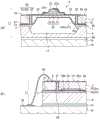
图1涉及第一实施方式,(a)是表示红外线检测元件的结构的概略分解立体图,(b)和(c)是第一实施方式涉及的表示红外线检测元件的结构的截面示意图。1 relates to the first embodiment, (a) is a schematic exploded perspective view showing the structure of the infrared detection element, and (b) and (c) are schematic cross-sectional views showing the structure of the infrared detection element according to the first embodiment.
图2的(a)是表示红外线检测部的结构的主要部分侧截面示意图,图2的(b)是表示电极和布线的结构的主要部分侧截面示意图。2( a ) is a schematic side sectional view showing the structure of the infrared detection unit, and FIG. 2( b ) is a schematic side sectional view showing the structure of electrodes and wiring.
图3是用于说明红外线检测元件的组装方法的示意图。FIG. 3 is a schematic diagram for explaining a method of assembling an infrared detection element.
图4是用于说明红外线检测元件的组装方法的示意图。FIG. 4 is a schematic diagram illustrating a method of assembling an infrared detection element.
图5是表示第二实施方式涉及的红外线检测元件的结构的主要部分侧截面示意图。5 is a schematic side sectional view of main parts showing the configuration of an infrared detection element according to a second embodiment.
图6是表示第三实施方式涉及的红外线摄像机的结构的框图。FIG. 6 is a block diagram showing the configuration of an infrared camera according to a third embodiment.
图7是表示第四实施方式涉及的驾驶辅助装置的结构的框图。7 is a block diagram showing the configuration of a driving assistance device according to a fourth embodiment.
图8是表示安装有驾驶辅助装置的汽车的立体示意图。Fig. 8 is a schematic perspective view showing an automobile equipped with a driving assistance device.
图9是表示第五实施方式涉及的安全设备的结构的框图。FIG. 9 is a block diagram showing the configuration of a security device according to a fifth embodiment.
图10是表示设置有安全设备的房屋的示意图。Fig. 10 is a schematic diagram showing a house provided with security equipment.
图11是表示第六实施方式涉及的游戏设备的控制器的结构的框图。11 is a block diagram showing the configuration of a controller of a game device according to a sixth embodiment.
图12是用于说明控制器的使用方法的示意图。Fig. 12 is a schematic diagram for explaining a method of using the controller.
图13是表示第七实施方式涉及的体温测定装置的结构的框图。Fig. 13 is a block diagram showing the configuration of a body temperature measurement device according to a seventh embodiment.
图14是表示第八实施方式涉及的指定物质探测装置的结构的框图。FIG. 14 is a block diagram showing the configuration of a designated substance detection device according to the eighth embodiment.
图15是表示变形例涉及的红外线检测元件的结构的主要部分侧截面示意图。15 is a schematic side sectional view of main parts showing the configuration of an infrared detection element according to a modified example.
具体实施方式Detailed ways
下面,将按照附图来说明在构造上具有特征的红外线检测元件的实施方式。此外,为了使各附图中的各部件变为在各图面中可识别程度的大小,使每个各部件比例尺不同地进行图示。Next, embodiments of an infrared detection element characteristic in structure will be described with reference to the drawings. In addition, in order that each member in each drawing may be recognizable in each drawing, each member is illustrated with a different scale.
(第一实施方式)(first embodiment)
在本实施方式中,将根据图1~图4来说明红外线检测元件和红外线检测元件的组装方法的特征例。In this embodiment, characteristic examples of the infrared detection element and the method of assembling the infrared detection element will be described based on FIGS. 1 to 4 .
(红外线检测元件)(infrared detection element)
图1的(a)是表示红外线检测元件的结构的分解立体示意图,图1的(b)和图1的(c)是表示红外线检测元件的结构的截面示意图。图1的(b)是沿图1的(a)的A-A’线的截面图,图1的(c)沿图1的(a)的B-B’线的截面图。如图1所示,红外线检测元件1的俯视图具备矩形的第一基板2。将在第一基板2的矩形中的正交的两边的方向设为X方向和Y方向。并且,将垂直方向设为-Z方向。将第一基板2的Z方向的面设为作为第一面的第一表面2a,将第一基板2的-Z方向的面设为作为第二面的第一背面2b。也就是说,第一表面2a与第一背面2b成为朝向相反侧的面。FIG. 1( a ) is an exploded schematic perspective view showing the structure of the infrared detection element, and FIGS. 1( b ) and 1 ( c ) are cross-sectional schematic views showing the structure of the infrared detection element. (b) of FIG. 1 is a cross-sectional view along line A-A' of (a) of FIG. 1 , and (c) of FIG. 1 is a cross-sectional view of line B-B' of (a) of FIG. 1 . As shown in FIG. 1 , the plan view of the
第一基板2的材料只要是具有刚性且具有绝缘性的材料就可以,能够使用硅、玻璃、陶瓷、强化塑料等。在第一基板2上形成半导体的电路时,使用由硅等构成的半导体基板。在本实施方式中,在例如第一基板2使用半导体基板。The material of the
在第一基板2的第一表面2a上,16个红外线检测部3被配置为纵横各四列的矩阵状。红外线检测部3是接收红外线并输出对应于受光量的电信号的元件。在第一背面2b上,在与各红外线检测部3相对的地方,形成有第一凹部4。对应一个红外线检测部3,形成有一个第一凹部4。由此,在设置有红外线检测部3的地方,第一基板2的厚度变薄。On the
在照射红外线时,红外线检测部3检测温度的上升量。因此,热难以从红外线检测部3传导的红外线检测部3更能够高灵敏度地检测红外线的照射量。在红外线检测部3所处的地方,由于第一基板2已经变薄,因而热就难以从红外线检测部3传导至第一基板2。另外,将由第一凹部4包围的空间作为第一空腔部5。在第一空腔部5中填充有空气。于是,由于第一空腔部5的空气难以流动,因而红外线检测元件1就难以将红外线检测部3的热放出至第一空腔部5。When infrared rays are irradiated, the
在第一表面2a上,电极6配置为一列。电极6是用于输出对应于红外线检测部3所检测的红外线的照射量的电信号的端子。On the
在第一基板2的-Z方向上,粘接膜7与第二基板8重叠配置。将第二基板8的Z方向的面设为作为第四面的第二背面8b,将第二基板8的-Z方向的面设为作为第三面的第二表面8a。也就是说,第二表面8a与第二背面8b成为朝向相反侧的面。于是,粘接膜7被配置在第一背面2b与第二背面8b之间,成为粘合第一背面2b与第二背面8b的膜。In the −Z direction of the
粘接膜7是将粘接剂固化而形成的膜。作为用于本实施方式的粘接剂,能够使用环氧类、聚氨酯类、丙烯酸类、硅类、聚酯类、酰亚胺类、聚酰胺酰亚胺类等。并且,也可以添加热固化引发剂等添加剂。The
第二基板8在第二背面8b的与第一凹部4相对的地方形成有第二凹部9。另外,如果将由第二凹部9包围的空间设为第二空腔部10,则在第二空腔部10中填充空气。于是,由于第二空腔部10的空气难以流动,因而就能够抑制红外线检测元件1将红外线检测部3的热量放出至第二基板8。The
第二空腔部10与第一空腔部5形成一个空腔部11。而且,以第二空腔部10的体积比第一空腔部5的体积大的方式形成第二空腔部10。第一凹部4的侧壁4a为相对于第一背面2b倾斜的斜面,第二凹部9的侧壁9a为相对于第二背面8b倾斜的斜面。而且,将第一凹部4的侧壁4a与第一背面2b交叉的地方作为第一外周部4b,将第二凹部9的侧壁9a与第二背面8b交叉的地方作为第二外周部9b。此时,第一外周部4b位于第二外周部9b的内侧,第一外周部4b以被第二外周部9b包围的方式配置。The
在粘接膜7固化之前,粘接膜7是具有粘性的液状的粘接剂,当向粘接剂施加压力时,粘接剂就会向空腔部11流动。此时,粘接剂在与第一外周部4b接触之前与第二外周部9b接触。然后,沿侧壁9a向第二凹部9流动。因此,通过使粘接剂向第二凹部9流动,从而能够使粘接膜7难以形成在第一凹部4上。Before the
侧壁9a为相对于第二背面8b倾斜的斜面。因此,向空腔部11流动的粘接膜7易于沿侧壁9a流动。其结果,粘接膜7向第二凹部9流动,能够使其难以附着于第一凹部4。另外,由于第二空腔部10的体积是比第一空腔部5的体积大的体积,因而粘接剂就难以填满第二凹部9。因此,能够使粘接膜7难以形成于第一凹部4。The
在第二基板8上互相邻接的第二凹部9之间,形成有作为槽部的凹部间槽部12。凹部间槽部12使各第二凹部9中的第二空腔部10连通。于是,在作为粘接膜7的材料的粘接剂积存在一个第二空腔部10中时,粘接剂通过在凹部间槽部12中流动,能够移动至相邻的第二空腔部10。因此,粘接剂就难以填满第二空腔部10,能够使粘接膜7难以形成于第一凹部4。Between the
在接近于第二基板8的侧面8c处的第二凹部9上,在第二凹部9与侧面8c之间形成有作为槽部的外部连通槽部13。外部连通槽部13使第二凹部9中的第二空腔部10和与侧面8c接触的外部气体连通。于是,在作为粘接膜7的材料的粘接剂积存在第二空腔部10中时,粘接剂能够在外部连通槽部13中流动并从侧面8c移动至红外线检测元件1的外部。因此,粘接剂就难以填满第二空腔部10,能够使粘接膜7难以形成于第一凹部4。On the second
在第二基板8的第二表面8a上,经由粘接膜14设置有封装基板15。而且,在封装基板15上形成有各种电路,封装基板15的电路与电极6被电连接。由此,能够输出红外线检测部3检测的红外线照射量的信号。On the
图2的(a)是表示红外线检测部的结构的主要部分侧截面示意图,图2的(b)是表示电极和布线的结构的主要部分侧截面示意图。如图2的(a)所示,在第一基板2的第一表面2a上形成有第一绝缘膜18。第一绝缘膜18是使由硅构成的第一基板2氧化而得的氧化膜,且具有电绝缘性的特性。2( a ) is a schematic side sectional view showing the structure of the infrared detection unit, and FIG. 2( b ) is a schematic side sectional view showing the structure of electrodes and wiring. As shown in FIG. 2( a ), a first insulating
在第一绝缘膜18的与第一凹部4相对的地方设置有下部电极19,并与下部电极19重叠地设置有热电体20。并且,在热电体20上设置有上部电极21。由下部电极19、热电体20、上部电极21等构成电容器22,电容器22的极化量根据温度不同而变化。A
以覆盖电容器22的方式设置有第二绝缘膜23。在第二绝缘膜23上形成有通到下部电极19的第一接触孔23a、和通到上部电极21的第二接触孔23b。在第一绝缘膜18和第二绝缘膜23上设置有第一布线24和第二布线25。第一布线24通过第一接触孔23a与下部电极19连接。同样,第二布线25通过第二接触孔23b与上部电极21连接。于是,红外线检测部3由第一绝缘膜18、电容器22、第二绝缘膜23、第一布线24以及第二布线25等构成。此外,可以与电容器22重叠地设置红外线吸收部件。由此,能够进一步改良红外线检测元件1的灵敏度。A second insulating
在第一基板2上形成有导通孔2c,在导通孔2c内的侧壁上形成有第三绝缘膜26。在第一背面2b和第一凹部4上还形成有第四绝缘膜27。第三绝缘膜26和第四绝缘膜27通过加热氧化而形成。在导通孔2c内设置有导电体28,由导通孔2c和导电体28构成贯通电极。在一个红外线检测部3中设置有两个贯通电极。贯通电极中的一个是与第一布线24连接的第一贯通电极29,贯通电极中的另一个是与第二布线25连接的第二贯通电极30。A via
在第一背面2b上,与第一贯通电极29连接地设置有背面第一布线33,与第二贯通电极30连接地设置有背面第二布线34。背面第一布线33经由第一贯通电极29、第一布线24与下部电极19连接。而且,背面第二布线34经由第二贯通电极30、第二布线25与上部电极21连接。因此,能够通过背面第一布线33和背面第二布线34来检测电容器22的极化量。On the
如图2的(b)所示,在第一基板2的第一背面2b上形成有集成电路35。在集成电路35上包括:驱动红外线检测部3的驱动电路、切换多个红外线检测部3的输出的控制电路等。集成电路35具备多个输入端子35a和输出端子35b。在输入端子35a上连接有背面第一布线33和背面第二布线34。而且,与输出端子35b连接地设置有背面第三布线36。As shown in FIG. 2( b ), an
并且,与背面第三布线36连接地形成有贯通第一基板2的第三贯通电极37。第三贯通电极37是与第一贯通电极29同样的结构。在第一表面2a上,与第三贯通电极37连接地设置有电极6。Furthermore, a third penetrating
在封装基板15中的设置有红外线检测元件1的面上设置有布线39,电极6与布线39用接合线40连接。由此,集成电路35输出至输出端子35b的电信号经由背面第三布线36、第三贯通电极37、电极6、接合线40被输出至布线39。
(红外线检测元件的组装方法)(Assembly method of infrared detection element)
接下来,将使用图3和图4来说明红外线检测元件的组装方法。图3和图4是用于说明红外线检测元件的组装方法的示意图。如图3的(a)所示,准备第二基板8。在第二基板8上形成有第二凹部9。第二凹部9能够采用光刻法和蚀刻法来形成。其形成方法是众所周知的,将省略说明。Next, a method of assembling the infrared detection element will be described using FIGS. 3 and 4 . 3 and 4 are schematic diagrams for explaining a method of assembling the infrared detection element. As shown in (a) of FIG. 3 , the
接着,在第二背面8b上涂覆粘接剂41。粘接剂41是固化时成为粘接膜7的材料。粘接剂41优选涂覆性良好、低粘度的材料。通过使粘接剂41扩展,能够在想要粘合的全部地方上形成粘接膜7。粘接剂41的涂覆方法能够采用网板印刷、凸版印刷、胶版印刷、喷墨法等印刷方法或者使用注射器进行涂覆的方法等。在本实施方式中,利用例如喷墨法来涂覆粘接剂41。Next, an adhesive 41 is applied on the
接着,如图3的(b)所示,准备第一基板2。在第一基板2上形成有第一空腔部5、第一贯通电极29、第二贯通电极30、红外线检测部3和各种布线。另外,在图中未显示的地方的第一基板2上形成有第三贯通电极37。这些构成要素能够采用溅射法或者蒸镀法等涂膜法、光刻法以及蚀刻法来形成。其形成方法是众所周知的,省略说明。Next, as shown in FIG. 3( b ), the
然后,通过使涂覆有粘接剂41的第二背面8b与第一背面2b重合而在第二基板8上重叠设置第一基板2。此时,粘接剂41被第二基板8与第一基板2夹着加压。于是,粘接剂41向空腔部11流动。此时,由于第二外周部9b位于包围第一外周部4b的地方,因而与第一外周部4b相比,粘接剂41会先到达第二外周部9b。侧壁9a与第二外周部9b连接,侧壁9a为相对于第二背面8b倾斜的斜面。于是,由于重力和表面张力作用于粘接剂41,因而粘接剂41就会沿侧壁9a而向第二凹部9流动。其结果,粘接剂41会难以附着于第一凹部4。Then, the
接着,通过加热干燥第二基板8和第一基板2而使粘接剂41固化。由此,粘接剂41变为粘接膜7,第二基板8与第一基板2粘合。由此,红外线检测元件1完成。Next, the adhesive 41 is cured by heating and drying the
然后,如图3的(c)所示,准备封装基板15,在封装基板15的、设置有红外线检测元件1的预定的地方涂覆粘接剂42。粘接剂42是固化时变为粘接膜14的材料。涂覆粘接剂42的方法没有特别限定,能够采用与涂覆粘接剂41的方法同样的方法。Next, as shown in FIG. 3( c ), the
接着,如图4的(a)所示,以重叠于粘接剂42的方式设置红外线检测元件1。然后,通过加热干燥设置有红外线检测元件1的封装基板15而将粘接剂42固化。由此,粘接剂42变为粘接膜14,红外线检测元件1被固定在封装基板15上。Next, as shown in FIG. 4( a ), the
在第二基板8中作为第二凹部9的底的底部9c将空腔部11遮蔽。因此,在粘接剂42被涂覆到第二表面8a上时,粘接剂42不会从第二表面8a流入第一凹部4。其结果,能够使粘接膜14难以形成于第一凹部4。The
然后,如图4的(b)所示,用接合线40连接红外线检测元件1上的电极6与封装基板15上的布线39之间。使用接合线40的接合方法是众所周知的,将省略详细的说明。通过以上的工序,红外线检测元件1被组装,并被封装于封装基板15。Then, as shown in FIG. 4( b ), the
如上所述,依照本实施方式,具有以下的效果:As described above, according to this embodiment, there are the following effects:
(1)依照本实施方式,第二外周部9b包围第一外周部4b。由此,在粘接剂41流入第一凹部4之前,粘接剂41将流入第二凹部9。因此,能够使粘接膜7难以形成于第一凹部4。(1) According to the present embodiment, the second outer
(2)依照本实施方式,第二基板8位于第一凹部4与第二表面8a之间。于是,底部9c将空腔部11遮蔽。因此,在为了封装红外线检测元件1而将粘接剂42附着于第二表面8a时,粘接剂42不会从第二表面8a流入空腔部11。其结果,能够防止粘接剂42附着于第一凹部4。(2) According to the present embodiment, the
(3)依照本实施方式,第二凹部9的侧壁9a为相对于第二背面8b倾斜的斜面。通过使粘接剂41流动时沿着斜面,则就会易于流动。因此,与第一凹部4相比,粘接剂41将流动至第二凹部9,因而能够使粘接膜难以形成于第一凹部4。(3) According to the present embodiment, the
(4)依照本实施方式,在第二凹部9与第二基板8的侧面8c之间具有外部连通槽部13。因此,流入第二凹部9的粘接剂41能够通过外部连通槽部13向第二基板8的侧面8c流动。其结果,第二凹部9会难以由粘接剂41充满,因而就能够使粘接膜难以形成于第一凹部4。(4) According to the present embodiment, the external communication groove portion 13 is provided between the second
(5)依照本实施方式,以连接多个第二凹部9之间的方式设置有凹部间槽部12。因此,流入第二凹部9的粘接剂41能够通过槽部而流动至其他的第二凹部9。其结果,第二凹部9会难以由粘接剂41充满,因而就能够使粘接膜难以形成于第一凹部4。(5) According to the present embodiment, the inter-recess grooves 12 are provided to connect the plurality of
(6)依照本实施方式,凹部间槽部12以及外部连通槽部13使各空腔部11与外部气体连通。由此,在粘接剂41固化而成为粘接膜7的过程中产生气体时,也能够防止空腔部11的压力上升。由此,能够使粘接膜7的厚度均匀化。通过使粘接膜7的厚度均匀化,能够使热量从第一基板2向第二基板8传导的速度变为相同。其结果,能够使红外线检测部3检测红外线的灵敏度的分散性缩小。(6) According to the present embodiment, the inter-recessed groove portion 12 and the external communication groove portion 13 communicate each
(第二实施方式)(Second Embodiment)
接下来,将使用图5的表示红外线检测元件的结构的主要部分侧截面示意图来说明红外线检测元件的一个实施方式。Next, one embodiment of the infrared detection element will be described using a main part side sectional schematic diagram showing the structure of the infrared detection element of FIG. 5 .
本实施方式与第一实施方式不同之处在于,图1的(b)所示的第二凹部9的形状不同这点。此外,关于与第一实施方式相同的方面,将省略说明。This embodiment differs from the first embodiment in that the shape of the second
即,在本实施方式中,如图5所示,红外线检测元件45具备第一基板2,在第一基板2上设置有多个红外线检测部3。而且,第一基板2与第二基板8通过粘接膜7粘合。对应一个红外线检测部3,在第一基板2上形成有一个第一凹部4。在第二基板8上,相对于两个第一凹部4,形成有一个第二凹部46。而且,由被第一凹部4包围的第一空腔部5和被第二凹部46包围的第二空腔部47形成一个空腔部48。因此,红外线检测部3与第一凹部4是相同的个数,而第二凹部46是比红外线检测部3少的个数。此外,在第二基板8上,可以对应三个以上的第一凹部4而形成有一个第二凹部46。由于能够简单地形成第二基板8的图案,因而能够易于检查第二基板8的形状。That is, in this embodiment, as shown in FIG. 5 , the
如上所述,依照本实施方式,具有以下的效果:As described above, according to this embodiment, there are the following effects:
(1)依照本实施方式,多个第一凹部4位于与一个第二凹部46相对的地方。因此,能够使第二凹部46的宽度变得比第一凹部4宽。因此,即使粘接剂41流入第二凹部46,第二凹部46也难以被粘接剂41充满,因而能够使粘接剂41难以附着在第一凹部4中。(1) According to the present embodiment, the plurality of
(2)依照本实施方式,第二凹部46的个数是比第一实施方式中的第二凹部9的个数少的个数。因此,能够使蚀刻第二基板8的图案的形状简单化,因而能够使第二基板8的成品率得以提高。其结果,能够高生产性地制造第二基板8。(2) According to this embodiment, the number of objects of the 2nd recessed
(第三实施方式)(third embodiment)
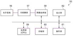
接下来,将使用图6的表示红外线摄像机的结构的框图来说明作为在红外线检测部中具备红外线检测元件的电子设备之一的红外线摄像机的一个实施方式。如图6所示,作为电子设备的红外线摄像机55包括光学系统56、光检测部57、图像处理部58、处理部59、存储部60、操作部61以及显示部62。Next, an embodiment of an infrared camera as one of electronic devices including an infrared detection element in an infrared detection unit will be described using the block diagram showing the configuration of the infrared camera in FIG. 6 . As shown in FIG. 6 , an
光学系统56包括例如一个或者多个透镜和驱动透镜的驱动部等。而且,向光检测部57进行物像的成像。另外,如果必要,也进行聚焦调整等。The
在光检测部57中,使用上述实施方式的红外线检测元件1或者红外线检测元件45。光检测部57除了被二维排列的检测器以外,还能够包括行选择电路(行驱动器)、经由列线读出来自检测器的数据的读取电路以及A/D转换部等。通过依次读取来自被二维排列的各检测器的数据,从而能够形成拍摄对象的图像数据。In the
图像处理部58根据来自光检测部57的数字图像数据(像素数据),进行图像补正处理等各种图像处理。The
处理部59进行红外线摄像机55的整体控制,进行红外线摄像机55内的各模块的控制。该处理部59由例如CPU等实现。存储部60用于存储各种信息,存储部60作为例如处理部59、图像处理部58的工作区域而起作用。操作部61成为用于用户操作红外线摄像机55的界面,操作部61由例如各种按钮或者GUI(Graphical User Interface,图形用户接口)画面等实现。显示部62用于显示例如由光检测部57取得的图像或者GUI画面等,显示部62由液晶显示器、有机EL显示器等各种显示器实现。The
这样,使用沿正交两轴方向二维配置红外线检测部3的光检测部57,能够提供热(光)分布图像。使用该光检测部57,能够构成红外线热像仪、车载用夜视仪或者监控摄像机等电子设备。In this manner, a heat (light) distribution image can be provided using the
当然,通过将一组(cell)或者多组的红外线检测部3用作传感器,也能够构成进行物体的物理信息分析(测定)的分析设备(测定设备)、检测火或者发热的安全设备、设置在工厂等中的FA(FactoryAutomation,工厂自动化)设备等各种电子设备。Of course, by using one or more sets of
如上所述,依照本实施方式,具有以下的效果:As described above, according to this embodiment, there are the following effects:
(1)依照本实施方式,红外线摄像机55具备光检测部57,在光检测部57中使用红外线检测元件1或者红外线检测元件45。由于光检测部57的红外线元件1或者红外线检测元件45高灵敏度地检测红外线,因而红外线摄像机55能够作为具备高灵敏度地检测红外线的红外线检测元件的电子设备。(1) According to the present embodiment, the
(第四实施方式)(Fourth embodiment)
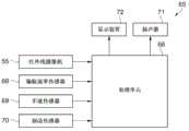
接下来,将使用图7和图8来说明作为使用了在红外线检测部中具备红外线检测元件的红外线摄像机的电子设备之一的驾驶辅助装置的一个实施方式。图7是表示驾驶辅助装置的结构的框图,图8是安装有驾驶辅助装置的汽车的立体示意图。Next, an embodiment of a driving assistance device as one of electronic devices using an infrared camera including an infrared detection element in an infrared detection unit will be described using FIGS. 7 and 8 . FIG. 7 is a block diagram showing the configuration of the driving assistance device, and FIG. 8 is a schematic perspective view of an automobile equipped with the driving assistance device.
如图7所示,作为电子设备的驾驶辅助装置65构成为包括:处理单元66,具备控制驾驶辅助装置65的CPU;红外线摄像机55,可以对车辆外部的规定摄像区域检测红外线;偏航速率传感器68,检测车辆的偏航速率;车速传感器69,检测车辆的行驶速度;制动传感器70,检测有无驾驶员的制动操作;扬声器71以及显示装置72。而且,本实施方式的红外线摄像机55使用与上述实施方式中的红外线摄像机55相同的照相机。As shown in FIG. 7 , the driving
该驾驶辅助装置65的处理单元66根据例如通过红外线摄像机55的拍摄得到的本汽车周边的红外线图像、和由各传感器68~70检测的有关本汽车的行驶状态的检测信号,检测存在于本汽车的行进方向前方的物体和行人等对象物,在判断为具有检测到的对象物与汽车接触的可能性时,由扬声器71或者显示装置72输出警报。The
如图8所示,红外线摄像机55在汽车的前部被配置在车辆宽度方向的中心附近。显示装置72在前窗不妨碍驾驶员的前方视野的位置上具备显示各种信息的HUD(Head Up Display,平视显示器)73等而构成。As shown in FIG. 8 , the
(1)依照本实施方式,驾驶辅助装置65具备红外线摄像机55。红外线摄像机55具备光检测部57,在光检测部57中使用红外线检测元件1或者红外线检测元件45。因此,驾驶辅助装置65能够作为具备红外线摄像机55的电子设备,该红外线摄像机55具备高灵敏度地检测红外线的红外线检测元件。(1) According to the present embodiment, the driving
(第五实施方式)(fifth embodiment)
接下来,将使用图9和图10来说明作为使用了在红外线检测部中具备红外线检测元件的红外线摄像机的电子设备之一的安全设备的一个实施方式。图9是表示安全设备的结构的框图,图10是表示设置有安全设备的房屋的示意图。Next, an embodiment of a security device as one of electronic devices using an infrared camera equipped with an infrared detection element in an infrared detection section will be described using FIGS. 9 and 10 . FIG. 9 is a block diagram showing the structure of the security device, and FIG. 10 is a schematic diagram showing a house in which the security device is installed.
如图9所示,作为电子设备的安全设备76至少具备:拍摄监控区域的红外线摄像机55和检测侵入监控区域的侵入者的人感传感器77。并且,安全设备76还具备:移动检测处理部78,通过处理从红外线摄像机55输出的图像数据来检测侵入监控区域的移动体;以及人感传感器检测处理部79,进行人感传感器77的检测处理。并且,安全设备76还具备:图像压缩部80,以规定的方式压缩从红外线摄像机55输出的图像数据;以及通信处理部81,发送被压缩的图像数据、侵入者检测信息或者接收从外部装置对安全设备76进行的各种设定信息等。并且,安全设备76构成为具备控制部82,该控制部82通过CPU对安全设备76的各处理部进行条件设定、处理指令发送、响应处理。而且,本实施方式的红外线摄像机55使用与上述实施方式中的红外线摄像机55相同的照相机。As shown in FIG. 9 , a
移动检测处理部78具备:图中未显示的缓冲存储器、输入缓冲存储器的输出的数据块(block data)平滑部以及输入数据块平滑部的输出的状态变化检测部。而且,移动检测处理部78的状态变化检测部利用如下原理来检测状态变化:如果监控区域为静止状态,则即使动态拍摄到的不同的帧也为相同的图像数据,而如果具有状态变化(移动体的侵入),则帧间的图像数据就会产生差异。The movement
如图10所示,安全设备76在屋檐下设置有红外线摄像机55和人感传感器77。而且,红外线摄像机55检测摄像区域83,人感传感器77检测检查区域84。As shown in FIG. 10 , the
(1)依照本实施方式,安全设备76具备红外线摄像机55。红外线摄像机55具备光检测部57,在光检测部57中使用红外线检测元件1或者红外线检测元件45。因此,安全设备76能够作为具备红外线摄像机55的电子设备,该红外线摄像机55具备高灵敏度地检测红外线的红外线检测元件。(1) According to the present embodiment, the
(第六实施方式)(sixth embodiment)
接下来,将使用图11和图12来说明作为使用了在红外线检测部中具备红外线检测元件的红外线摄像机的电子设备之一的游戏设备的一个实施方式。图11是表示游戏设备的控制器的结构的框图,图12是用于说明控制器的使用方法的示意图。Next, an embodiment of a game device as one of electronic devices using an infrared camera equipped with an infrared detection element in an infrared detection section will be described using FIGS. 11 and 12 . FIG. 11 is a block diagram showing the configuration of a controller of the game device, and FIG. 12 is a schematic diagram for explaining how to use the controller.
如图11所示,作为游戏设备使用的电子设备的控制器87构成为具备:摄像信息运算单元88、操作开关89、加速度传感器90、连接器91、处理器92以及无线模块93。As shown in FIG. 11 , a
摄像信息运算单元88具有摄像单元94和用于处理由该摄像单元94拍摄到的图像数据的图像处理电路95。摄像单元94包括光检测部96,在其前方,配置有仅使红外线通过的作为滤波器的红外线滤波器97以及透镜等光学系统98。并且,图像处理电路95处理由摄像单元94得到的红外线图像数据,检测高亮度部分,检测出其重心位置、面积并输出这些数据。在本实施方式的光检测部96中,使用红外线检测元件1或者红外线检测元件45。The imaging
处理器92将从操作开关89发送的操作数据、从加速度传感器90发送的加速度数据以及高亮度部分数据作为一系列的控制数据而输出。无线模块93用该控制数据调制规定频率的载波,并从天线890输出作为电波信号。The
此外,通过设置在控制器87上的连接器91输入的数据也由处理器92进行与上述的数据同样的处理,并作为控制数据经由无线模块93和天线890输出。In addition, data input through the
如图12所示,游戏设备99具备:控制器87、游戏设备主体100、显示器101、LED模块102以及LED模块103,玩家104能够用一只手握持控制器87玩游戏。于是,如果使控制器87的摄像单元94朝向显示器101的画面105,则由摄像单元94检测从设置在显示器101的附近的两个LED模块102和LED模块103输出的红外线,控制器87将两个LED模块102、103的位置、面积信息取得作为高亮度点的信息。亮点的位置、大小的数据由控制器87以无线的方式发送至游戏设备主体100,由游戏设备主体100接收。如果玩家104使控制器87移动,则亮点的位置、大小的数据就会变化,因而利用这一点,游戏设备主体100能够取得对应于控制器87的移动的操作信号,因而能够按照该移动而进行游戏。As shown in FIG. 12 , the game device 99 includes: a
如上所述,依照本实施方式,具有以下的效果:As described above, according to this embodiment, there are the following effects:
(1)依照本实施方式,游戏设备99的控制器87具备光检测部96,在光检测部96中使用红外线检测元件1或者红外线检测元件45。由于光检测部96的红外线元件1或者红外线检测元件45高灵敏度地检测红外线,因而游戏设备99能够作为具有控制器87的电子设备,该控制器87具备高灵敏度地检测红外线的红外线检测元件。(1) According to the present embodiment, the
(第七实施方式)(seventh embodiment)
接下来,将使用图13来说明作为使用了在红外线检测部中具备红外线检测元件的红外线摄像机的电子设备之一的体温测定装置的一个实施方式。图13是表示体温测定装置的结构的框图。Next, an embodiment of a body temperature measurement device as one of electronic devices using an infrared camera including an infrared detection element in an infrared detection unit will be described using FIG. 13 . Fig. 13 is a block diagram showing the configuration of the body temperature measurement device.
如图13所示,作为电子设备的体温测定装置108构成为具备红外线摄像机55、体温分析装置109、信息通信装置110以及电缆111。本实施方式的红外线摄像机55使用与第三实施方式的红外线摄像机55相同的照相机。As shown in FIG. 13 , a body
红外线摄像机55拍摄规定的对象区域,并将拍摄到的对象者112的图像信息经由电缆111发送至体温分析装置109。体温分析装置109包括:图像读取处理单元,读取由红外线摄像机55发送的热分布图像;以及体温分析处理单元,根据由图像读取处理单元发送的数据和图像分析设定表来制作体温分析表,体温分析装置109根据体温分析表而将体温信息发送用数据发送给信息通信装置110。该体温信息发送用数据可以含有对应于体温异常情况的规定的数据。另外,在判断为摄影区域内含有多个对象者112时,可以将对象者112的人数和体温异常者的人数的信息包含在体温信息发送用数据中。The
如上所述,依照本实施方式,具有以下的效果:As described above, according to this embodiment, there are the following effects:
(1)依照本实施方式,体温测定装置108具备红外线摄像机55。红外线摄像机55具备光检测部57,在光检测部57中使用红外线检测元件1或者红外线检测元件45。因此,体温测定装置108能够作为具备红外线摄像机55的电子设备,该红外线摄像机55具备高灵敏度地检测红外线的红外线检测元件。(1) According to the present embodiment, the body
(第八实施方式)(eighth embodiment)
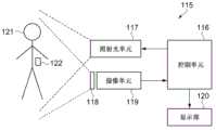
接下来,将使用图14的表示指定物质探测装置的结构的框图来说明作为在光检测部中具备红外线检测元件的电子设备之一的指定物质探测装置的一个实施方式。Next, an embodiment of a designated substance detection device as one of electronic devices including an infrared detection element in a photodetection unit will be described using the block diagram of FIG. 14 showing the configuration of the designated substance detection device.
如图14所示,作为电子设备的指定物质探测装置115构成为具备控制单元116、照射光单元117、光学滤波器118、摄像单元119以及显示部120。摄像单元119具备图中未显示的透镜等光学系统和光检测部,该光检测部构成为包括红外线检测元件1,红外线检测元件1将第一实施方式的红外线检测元件1的红外线检测部3所具备的光吸收材料的吸收波长设定为太赫兹区域(terahertz range)。或者,该光检测部构成为包括红外线检测元件45,红外线检测元件45将第二实施方式的红外线检测元件45的红外线检测部3所具备的光吸收材料的吸收波长设定为太赫兹区域。As shown in FIG. 14 , a designated
控制单元116包括控制本装置整体的系统控制器,该系统控制器控制被包括在控制单元中的光源驱动部和图像处理单元。照射光单元117包括:射出波长在100μm~1000μm范围内的作为电磁波的太赫兹光的激光装置和光学系,将太赫兹光照射至检查对象的人物121。从人物121发出的反射太赫兹光经由仅使作为探测对象的指定物质122的分光光谱通过的光学滤波器118而被摄像单元119所接收。由摄像单元119生成的图像信号由控制单元116的图像处理单元实施规定的图像处理,其图像信号被输出给显示部120。于是,接收信号的强度根据在人物121的衣服内等是否存在指定物质122而不同,因而能够判别指定物质122的存在。The
如上所述,依照本实施方式,具有以下的效果:As described above, according to this embodiment, there are the following effects:
(1)依照本实施方式,指定物质探测装置115在摄像单元119中具备光检测部,在光检测部中使用红外线检测元件1或者红外线检测元件45。由于光检测部57的红外线元件1或者红外线检测元件45高灵敏度地检测红外线,因而指定物质探测装置115能够作为在摄像单元119中具备高灵敏度地检测红外线的红外线检测元件的电子设备。(1) According to the present embodiment, the designated
以上,虽然对几个实施方式进行了说明,但是,能够进行在实质上不脱离本发明的新颖事项和效果的多种变型,这一点对于本领域的普通技术人员来说,是能够容易理解的。因此,这些变型实例应当全部被包括在本发明的范围内。例如,在说明书或者附图中,至少一次与更加广义或者同义的不同术语一起记载的术语,在说明书或者附图中的任何地方都能够替换为该不同的术语。Although several embodiments have been described above, those skilled in the art can easily understand that various modifications can be made without substantially departing from the novel matters and effects of the present invention. . Therefore, these modified examples should all be included in the scope of the present invention. For example, in the specification or the drawings, a term that is described together with a different term in a broader or synonymous sense at least once can be replaced by the different term anywhere in the specification or the drawings.
本发明能够广泛地适用于各种热电体型检测器。不论要检测的光的波长如何。另外,热电体型检测器、热电体型检测装置、或者具有它们的电子设备也能够适用于例如在所供给的热量与流体吸收的热量均衡的条件下检测流体的流量的流量传感器(flow sensor)等。能够设置本发明的热电体型检测器或者热电体型检测装置来代替设在该流量传感器上的热电偶等,并能够将光以外作为检测对象。The present invention can be widely applied to various pyroelectric detectors. Regardless of the wavelength of the light to be detected. In addition, pyroelectric detectors, pyroelectric detection devices, or electronic devices having them can also be applied to, for example, flow sensors (flow sensors) that detect the flow rate of a fluid under the condition that the heat supplied and the heat absorbed by the fluid are in balance. The pyroelectric detector or pyroelectric detection device of the present invention can be provided instead of the thermocouple or the like provided on the flow sensor, and other than light can be used as a detection object.
此外,本实施方式并不仅限于上述的实施方式,也能够施加各种变更或者改良。以下,将说明变形例。In addition, this embodiment is not limited to the above-mentioned embodiment, Various changes and improvements can be added. Hereinafter, modified examples will be described.
(变形例1)(Modification 1)
在上述第一实施方式中,形成在第二基板8上的第二凹部9的深度形成得比第二基板8的厚度浅。图15是表示红外线检测元件的结构的主要部分侧截面示意图。如图15的红外线检测元件49所示的那样,形成在第二基板8的与第一凹部4相对的地方的第二凹部50可以贯通第二基板8。于是,可以将被第二凹部50包围的第二空腔部51的体积形成得比粘接剂41和粘接剂42流入第二凹部50的体积大的体积。在这种情况下,由于粘接剂41和粘接剂42也不会流入第一空腔部5,因而能够使粘接剂41和粘接剂42难以附着于第一凹部4。In the first embodiment described above, the depth of the second
(变形例2)(Modification 2)
在上述第一实施方式中,第一凹部4未贯通第一基板2,而第二凹部4可以贯通第一基板2。而且,可以用梁支撑红外线检测部3。此时,由于难以从红外线检测部3向第一基板2传动而放热,因而能够提高红外线检测部3的灵敏度。In the above-mentioned first embodiment, the first
(变形例3)(Modification 3)
在上述第一实施方式中,侧壁9a为相对于第二背面8b倾斜的斜面。在侧壁9a相对于粘接剂41而表面张力高时,侧壁9a可以与第二背面8b正交。能够使重力作用于粘接剂41而易于移动至底部9c。In the first embodiment described above, the
(变形例4)(Modification 4)
在上述第一实施方式中,红外线检测元件1纵横各配置四个红外线检测部3。红外线检测部3的个数没有特别限定,可以为1~15个,也可以为17个以上。即使在这种情况下,通过设置形成有第二凹部9的第二基板8,也能够防止粘接剂41附着于第一凹部4。In the above-described first embodiment, the
(变形例5)(Modification 5)
在上述第一实施方式中,在相互邻接的所有第二凹部9之间都设置有凹部间槽部12。凹部间槽部12可以不设置在相互邻接的所有第二凹部9之间。可以从一个第二凹部9开始设置一个凹部间槽部12或者外部连通槽部13。由于能够减少蚀刻第二基板8的量,因而能够高生产性地制造第二基板8。In the above-described first embodiment, the inter-recess grooves 12 are provided between all the
(变形例6)(Modification 6)
在所述第一实施方式中,红外线检测元件1具备集成电路35。在红外线检测部3的个数较少时,可以不具备集成电路35。可以从与红外线检测部3连接的第一布线24和第二布线25直接通过接合线40与封装基板15的布线39连接。由于没有集成电路35,因而高能够生产性地制造红外线检测元件。In the first embodiment, the
符号说明Symbol Description
1 红外线检测元件 2 第一基板1
2a 作为第一面的第一表面 2b 作为第二面的第一背面2a as the first face of the
3 红外线检测部 4 第一凹部3 Infrared
4b 第一外周部 7 粘接膜4b First
8 第二基板 8a 作为第三面的第二表面8 The
8b 作为第四面的第二背面 8c 侧面8b second back as fourth side 8c side
9、46、50 第二凹部 9a 侧壁9, 46, 50 second
9b 第二外周部 9c 底部9b second
11、48 空腔部 12 作为槽部的凹部间槽部11, 48 Cavity part 12 The inter-recess groove part as the groove part
13 作为槽部的外部连通槽部 42 粘接剂13 External communication groove portion as
55 作为电子设备的红外线摄像机 57、96 光检测部55 Infrared camera as an
65 作为电子设备的驾驶辅助装置 76 作为电子设备的安全设备65 Driving aids as
87 作为电子设备的控制器87 As a controller for electronic equipment
108 作为电子设备的体温测定装置108 Body temperature measuring devices as electronic equipment
115 作为电子设备的指定物质探测装置115 Specified substance detection devices as electronic equipment
Claims (7)
Translated fromChineseApplications Claiming Priority (2)
| Application Number | Priority Date | Filing Date | Title |
|---|---|---|---|
| JP2011170778AJP5853476B2 (en) | 2011-08-04 | 2011-08-04 | Infrared detector and electronic device |
| JP2011-170778 | 2011-08-04 |
Publications (1)
| Publication Number | Publication Date |
|---|---|
| CN102914372Atrue CN102914372A (en) | 2013-02-06 |
Family
ID=47612843
Family Applications (1)
| Application Number | Title | Priority Date | Filing Date |
|---|---|---|---|
| CN201210273610XAPendingCN102914372A (en) | 2011-08-04 | 2012-08-02 | Infrared detecting element and electronic device |
Country Status (3)
| Country | Link |
|---|---|
| US (1) | US9285274B2 (en) |
| JP (1) | JP5853476B2 (en) |
| CN (1) | CN102914372A (en) |
Cited By (5)
| Publication number | Priority date | Publication date | Assignee | Title |
|---|---|---|---|---|
| CN103390630A (en)* | 2013-07-17 | 2013-11-13 | 深圳市华星光电技术有限公司 | Infrared detecting device based on organic p-n junctions, manufacturing method thereof and infrared image detector using device |
| CN106054275A (en)* | 2016-08-12 | 2016-10-26 | 米运田 | Infrared detection edge alignment device |
| CN110577186A (en)* | 2019-09-12 | 2019-12-17 | 南通大学 | A MEMS infrared detector three-dimensional packaging structure and manufacturing method thereof |
| CN114184279A (en)* | 2021-11-29 | 2022-03-15 | 陕西省地方电力(集团)有限公司 | A Temperature Monitoring System Based on MESH Network Applied to Tunnel Cable Monitoring |
| CN119063842A (en)* | 2024-11-05 | 2024-12-03 | 南通南洋照明科技有限公司 | LED light source detection equipment and detection method |
Families Citing this family (8)
| Publication number | Priority date | Publication date | Assignee | Title |
|---|---|---|---|---|
| JP2014235146A (en)* | 2013-06-05 | 2014-12-15 | セイコーエプソン株式会社 | Terahertz wave detecting apparatus, camera, imaging apparatus, and measuring apparatus |
| CN105452826B (en)* | 2013-08-09 | 2019-07-23 | 世美特株式会社 | Infrared temperature sensor and device using infrared temperature sensor |
| KR102355553B1 (en) | 2016-09-02 | 2022-01-26 | 소니 세미컨덕터 솔루션즈 가부시키가이샤 | imaging device |
| KR20180069147A (en)* | 2016-12-14 | 2018-06-25 | 만도헬라일렉트로닉스(주) | Apparatus for warning pedestrian in vehicle |
| US10448864B1 (en) | 2017-02-24 | 2019-10-22 | Nokomis, Inc. | Apparatus and method to identify and measure gas concentrations |
| CN109786498B (en)* | 2018-12-10 | 2021-04-06 | 华南理工大学 | Infrared detection element based on two-dimensional semiconductor material and preparation method thereof |
| CN110967119B (en)* | 2019-11-18 | 2020-10-27 | 中国空间技术研究院 | Ultra-wide waveband uncooled infrared detector with single-layer structure and preparation method thereof |
| US20240145324A1 (en)* | 2021-06-03 | 2024-05-02 | Mitsubishi Electric Corporation | Semiconductor sensor and method for manufacturing same |
Citations (5)
| Publication number | Priority date | Publication date | Assignee | Title |
|---|---|---|---|---|
| US5450053A (en)* | 1985-09-30 | 1995-09-12 | Honeywell Inc. | Use of vanadium oxide in microbolometer sensors |
| JPH08122160A (en)* | 1994-10-24 | 1996-05-17 | Ricoh Seiki Co Ltd | Heat-dependence detection device |
| CN101568813A (en)* | 2006-10-20 | 2009-10-28 | 模拟装置公司 | Die temperature sensors |
| CN101819063A (en)* | 2009-12-29 | 2010-09-01 | 南京邮电大学 | Micro-spectrometer for phase modulation groove array |
| CN102901567A (en)* | 2011-07-29 | 2013-01-30 | 江苏物联网研究发展中心 | Thermopile infrared detector, array and preparation method of thermopile infrared detector |
Family Cites Families (9)
| Publication number | Priority date | Publication date | Assignee | Title |
|---|---|---|---|---|
| JP3121424B2 (en) | 1992-02-28 | 2000-12-25 | 浜松ホトニクス株式会社 | Semiconductor photodetector |
| JPH0622944U (en)* | 1992-08-26 | 1994-03-25 | 松下電工株式会社 | Sensor chip mounting structure |
| JPH0677504A (en) | 1992-08-26 | 1994-03-18 | Matsushita Electric Works Ltd | Mounting method for chip for sensor |
| JPH06249708A (en)* | 1993-02-23 | 1994-09-09 | Nissan Motor Co Ltd | Infrared sensor and manufacture thereof |
| US20040187904A1 (en) | 2003-02-05 | 2004-09-30 | General Electric Company | Apparatus for infrared radiation detection |
| JP4228232B2 (en) | 2005-02-18 | 2009-02-25 | 日本電気株式会社 | Thermal infrared detector |
| JP2007258523A (en)* | 2006-03-24 | 2007-10-04 | Matsushita Electric Ind Co Ltd | Semiconductor device and manufacturing method thereof |
| JP5404141B2 (en) | 2008-06-13 | 2014-01-29 | キヤノン株式会社 | Ultrasonic device and control method thereof |
| JP2010050406A (en)* | 2008-08-25 | 2010-03-04 | Sharp Corp | Semiconductor device, method of manufacturing semiconductor device, and electronic apparatus |
- 2011
- 2011-08-04JPJP2011170778Apatent/JP5853476B2/ennot_activeExpired - Fee Related
- 2012
- 2012-07-11USUS13/546,318patent/US9285274B2/ennot_activeExpired - Fee Related
- 2012-08-02CNCN201210273610XApatent/CN102914372A/enactivePending
Patent Citations (5)
| Publication number | Priority date | Publication date | Assignee | Title |
|---|---|---|---|---|
| US5450053A (en)* | 1985-09-30 | 1995-09-12 | Honeywell Inc. | Use of vanadium oxide in microbolometer sensors |
| JPH08122160A (en)* | 1994-10-24 | 1996-05-17 | Ricoh Seiki Co Ltd | Heat-dependence detection device |
| CN101568813A (en)* | 2006-10-20 | 2009-10-28 | 模拟装置公司 | Die temperature sensors |
| CN101819063A (en)* | 2009-12-29 | 2010-09-01 | 南京邮电大学 | Micro-spectrometer for phase modulation groove array |
| CN102901567A (en)* | 2011-07-29 | 2013-01-30 | 江苏物联网研究发展中心 | Thermopile infrared detector, array and preparation method of thermopile infrared detector |
Cited By (6)
| Publication number | Priority date | Publication date | Assignee | Title |
|---|---|---|---|---|
| CN103390630A (en)* | 2013-07-17 | 2013-11-13 | 深圳市华星光电技术有限公司 | Infrared detecting device based on organic p-n junctions, manufacturing method thereof and infrared image detector using device |
| CN103390630B (en)* | 2013-07-17 | 2015-11-11 | 深圳市华星光电技术有限公司 | Based on infrared detector and preparation method thereof and the infrared image detection device using this device of organic p-n junction |
| CN106054275A (en)* | 2016-08-12 | 2016-10-26 | 米运田 | Infrared detection edge alignment device |
| CN110577186A (en)* | 2019-09-12 | 2019-12-17 | 南通大学 | A MEMS infrared detector three-dimensional packaging structure and manufacturing method thereof |
| CN114184279A (en)* | 2021-11-29 | 2022-03-15 | 陕西省地方电力(集团)有限公司 | A Temperature Monitoring System Based on MESH Network Applied to Tunnel Cable Monitoring |
| CN119063842A (en)* | 2024-11-05 | 2024-12-03 | 南通南洋照明科技有限公司 | LED light source detection equipment and detection method |
Also Published As
| Publication number | Publication date |
|---|---|
| JP2013036766A (en) | 2013-02-21 |
| JP5853476B2 (en) | 2016-02-09 |
| US20130032717A1 (en) | 2013-02-07 |
| US9285274B2 (en) | 2016-03-15 |
Similar Documents
| Publication | Publication Date | Title |
|---|---|---|
| CN102914372A (en) | Infrared detecting element and electronic device | |
| JP3998788B2 (en) | Sensor and fire extinguishing system using this sensor | |
| US9275974B2 (en) | Optical sensor chip device and corresponding production method | |
| US9006856B2 (en) | Thermal electromagnetic wave detection element, method for producing thermal electromagnetic wave detection element, thermal electromagnetic wave detection device, and electronic apparatus | |
| US20230125605A1 (en) | Semiconductor device | |
| US20180366385A1 (en) | Glass interposer module, imaging device, and electronic apparatus | |
| CN110214376B (en) | Semiconductor device and electronic apparatus | |
| WO2020178700A1 (en) | Mems package with double-sided mirror | |
| JP5662225B2 (en) | Infrared sensor | |
| JP4208775B2 (en) | Photoelectric signal detector | |
| JP2013057526A (en) | Infrared sensor, manufacturing method therefor, and electronic apparatus | |
| JP2006317232A (en) | Infrared sensor | |
| US9534959B2 (en) | Infrared sensor package | |
| US8835208B2 (en) | Method for manufacturing detecting element, method for manufacturing imaging device, detecting element, imaging device, and electronic device | |
| CN105502275B (en) | The integrating device and its manufacture method of optical chip and inertial sensor | |
| JP6508471B2 (en) | Light sensor, infrared light sensor and electronic equipment | |
| JP2013246119A (en) | Thermal type electromagnetic wave detector, method of manufacturing the same, and electronic apparatus | |
| JP2011216741A (en) | Optical device and method for manufacturing optical device | |
| JP2016042080A (en) | Digital radiation sensor package | |
| JP5915020B2 (en) | Infrared detector and electronic device | |
| JP2014059249A (en) | Thermal electromagnetic wave detection element chip and thermal electromagnetic wave detector, and electronic apparatus | |
| JP5906757B2 (en) | Thermal electromagnetic wave detector, method for manufacturing the same, and electronic device | |
| JP6007477B2 (en) | Pyroelectric detector, pyroelectric detector and electronic device | |
| JP2013217786A (en) | Thermal electromagnetic wave detection element, method for manufacturing thermal electromagnetic wave detection element, thermal electromagnetic wave detection device, and electronic apparatus | |
| JP2013246079A (en) | Thermal type electromagnetic wave detector, electronic apparatus, and terahertz camera |
Legal Events
| Date | Code | Title | Description |
|---|---|---|---|
| C06 | Publication | ||
| PB01 | Publication | ||
| C10 | Entry into substantive examination | ||
| SE01 | Entry into force of request for substantive examination | ||
| WD01 | Invention patent application deemed withdrawn after publication | ||
| WD01 | Invention patent application deemed withdrawn after publication | Application publication date:20130206 |