CN102902443A - Touch detection component, touch control device and portable electronic equipment - Google Patents
Touch detection component, touch control device and portable electronic equipmentDownload PDFInfo
- Publication number
- CN102902443A CN102902443ACN2012100936811ACN201210093681ACN102902443ACN 102902443 ACN102902443 ACN 102902443ACN 2012100936811 ACN2012100936811 ACN 2012100936811ACN 201210093681 ACN201210093681 ACN 201210093681ACN 102902443 ACN102902443 ACN 102902443A
- Authority
- CN
- China
- Prior art keywords
- electrode
- group
- sensing
- touch detection
- shaped
- Prior art date
- Legal status (The legal status is an assumption and is not a legal conclusion. Google has not performed a legal analysis and makes no representation as to the accuracy of the status listed.)
- Granted
Links
Images


Classifications
- G—PHYSICS
- G06—COMPUTING OR CALCULATING; COUNTING
- G06F—ELECTRIC DIGITAL DATA PROCESSING
- G06F3/00—Input arrangements for transferring data to be processed into a form capable of being handled by the computer; Output arrangements for transferring data from processing unit to output unit, e.g. interface arrangements
- G06F3/01—Input arrangements or combined input and output arrangements for interaction between user and computer
- G06F3/03—Arrangements for converting the position or the displacement of a member into a coded form
- G06F3/041—Digitisers, e.g. for touch screens or touch pads, characterised by the transducing means
- G06F3/044—Digitisers, e.g. for touch screens or touch pads, characterised by the transducing means by capacitive means
- G06F3/0443—Digitisers, e.g. for touch screens or touch pads, characterised by the transducing means by capacitive means using a single layer of sensing electrodes
- G—PHYSICS
- G06—COMPUTING OR CALCULATING; COUNTING
- G06F—ELECTRIC DIGITAL DATA PROCESSING
- G06F3/00—Input arrangements for transferring data to be processed into a form capable of being handled by the computer; Output arrangements for transferring data from processing unit to output unit, e.g. interface arrangements
- G06F3/01—Input arrangements or combined input and output arrangements for interaction between user and computer
- G06F3/03—Arrangements for converting the position or the displacement of a member into a coded form
- G06F3/041—Digitisers, e.g. for touch screens or touch pads, characterised by the transducing means
- G06F3/044—Digitisers, e.g. for touch screens or touch pads, characterised by the transducing means by capacitive means
- G06F3/0448—Details of the electrode shape, e.g. for enhancing the detection of touches, for generating specific electric field shapes, for enhancing display quality
Landscapes
- Engineering & Computer Science (AREA)
- General Engineering & Computer Science (AREA)
- Theoretical Computer Science (AREA)
- Human Computer Interaction (AREA)
- Physics & Mathematics (AREA)
- General Physics & Mathematics (AREA)
- Quality & Reliability (AREA)
- Position Input By Displaying (AREA)
- Electronic Switches (AREA)
- Measurement Of Resistance Or Impedance (AREA)
- Measurement Of Length, Angles, Or The Like Using Electric Or Magnetic Means (AREA)
Abstract
Translated fromChineseDescription
Translated fromChinese技术领域technical field
本发明涉及电子设备设计及制造技术领域,尤其涉及一种触摸检测组件、具有所述触摸检测组件的触控装置以及便携式电子设备。The invention relates to the technical field of electronic equipment design and manufacture, and in particular to a touch detection component, a touch control device with the touch detection component, and a portable electronic device.
背景技术Background technique
目前触摸检测组件(触摸屏)在手机,PDA(个人数字助理),GPS(全球定位系统),PMP(MP3,MP4等),甚至平板电脑等电子设备中得到了应用。触摸屏具有触控操作简单、便捷、人性化的优点,因此触摸屏有望成为人机互动的最佳界面而在便携式设备中得到了广泛应用。Currently, touch detection components (touch screens) are used in electronic devices such as mobile phones, PDAs (Personal Digital Assistants), GPS (Global Positioning System), PMPs (MP3, MP4, etc.), and even tablet computers. The touch screen has the advantages of simple, convenient and humanized touch operation, so the touch screen is expected to become the best interface for human-computer interaction and has been widely used in portable devices.
电容触摸检测组件通常被分为自电容式和互电容式两类。现有的单层自电容触摸屏是在玻璃表面有用ITO(Indium Tin Oxides,纳米铟锡金属氧化物)制成的条形的扫描电极。ITO是一种有固定电阻率的导电物质,其在基材上的一致性比较高,从电阻屏的线性度就可以证明这一点。这些电极和地以及电路等周围环境构成一个电容的两极。当用手或触摸笔触摸的时候就会并联一个电容到电路中去,从而使该条扫描线上的总体电容量有所改变。在扫描的时候,控制IC通过特定的扫描方式扫描各个感应元件,并根据扫描前后的电容变化来确定触摸点的位置,从而达到人机对话交流。一般情况下电容触摸屏是和TFT(Thin Film Transistor,薄膜场效应晶体管)LCD一起配对工作,而且是放置在LCD的上面。Capacitive touch detection components are generally classified into two types: self-capacitive and mutual-capacitive. The existing single-layer self-capacitance touch screen is a strip-shaped scanning electrode made of ITO (Indium Tin Oxides, nanometer indium tin oxides) on the glass surface. ITO is a conductive substance with a fixed resistivity, and its consistency on the substrate is relatively high, which can be proved from the linearity of the resistive screen. These electrodes and the surrounding environment such as the ground and the circuit form the two poles of a capacitor. When touched by a hand or a touch pen, a capacitor will be connected in parallel to the circuit, so that the overall capacitance of the scanning line will be changed. When scanning, the control IC scans each sensing element through a specific scanning method, and determines the position of the touch point according to the capacitance change before and after scanning, so as to achieve human-machine dialogue. Under normal circumstances, the capacitive touch screen is paired with TFT (Thin Film Transistor, Thin Film Field Effect Transistor) LCD, and it is placed on top of the LCD.
图1示出了一种传统自电容式触摸检测组件。该自电容式触摸检测组件主要有双层的菱形结构感应单元100’和200’,其检测原理是对X轴和Y轴分别扫描,如果检测到某个交叉点的电容变化超出了预设范围,则将该行和列的交叉点作为触摸坐标。虽然该自电容式触摸检测组件的线性度较好,但是经常有鬼点出现,难以实现多点触摸。此外,由于采用双层屏,也会导致结构及成本大幅增加,并且菱形结构在电容变化量很小的情况下会出现坐标飘移,受外界干扰影响大。FIG. 1 shows a traditional self-capacitive touch detection component. The self-capacitance touch detection component mainly includes double-layer rhombic structure sensing units 100' and 200'. The detection principle is to scan the X-axis and Y-axis respectively. If the capacitance change of a certain cross point exceeds the preset range , the intersection of the row and column is used as the touch coordinates. Although the linearity of the self-capacitive touch detection component is good, ghost points often appear and it is difficult to realize multi-point touch. In addition, due to the use of double-layer screens, the structure and cost will also be greatly increased, and the rhombus structure will have coordinate drift when the capacitance change is small, and it will be greatly affected by external interference.
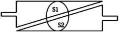
图2a示出了另一种传统自电容式触摸检测组件。该自电容式触摸检测组件采用三角形图形屏结构。该自电容式触摸检测组件包括基板300’、设置在基板300’之上的多个三角形感应单元400’、和每个三角形感应单元400’相连的多个电极500’。图2b示出了三角形自电容式触摸检测组件的检测原理。如图2b所示,椭圆表示手指,S1、S2表示手指与两个三角形感应单元的接触面积。假设坐标原点在左下角,则横坐标X=S2/(S1+S2)*P,其中,P为分辨率。当手指向右移动时,由于S2不是线性增大,所以X坐标存在一个偏差。从上述原理可以看出,传统的三角形感应单元是单端检测,即只从一个方向检测,然后通过算法算出两个方向的坐标。虽然该自电容式触摸检测组件结构简单,但并没有针对屏幕的电容感应进行优化,电容变化量小,从而导致信噪比不够。此外,由于该感应单元为三角形,当手指横向移动时面积不是线性增大,因此线性度较差,导致了坐标计算发生偏移,线性度不够好。Fig. 2a shows another conventional self-capacitive touch detection component. The self-capacitive touch detection component adopts a triangular graphic screen structure. The self-capacitive touch detection component includes a substrate 300', a plurality of triangular sensing units 400' disposed on the substrate 300', and a plurality of electrodes 500' connected to each triangular sensing unit 400'. Fig. 2b shows the detection principle of the triangular self-capacitive touch detection component. As shown in Figure 2b, the ellipse represents the finger, and S1 and S2 represent the contact area between the finger and the two triangular sensing units. Assuming that the coordinate origin is at the lower left corner, then the abscissa X=S2/(S1+S2)*P, where P is the resolution. When the finger moves to the right, since S2 does not increase linearly, there is a deviation in the X coordinate. It can be seen from the above principles that the traditional triangular sensing unit is single-ended detection, that is, it only detects from one direction, and then calculates the coordinates of the two directions through an algorithm. Although the self-capacitive touch detection component has a simple structure, it is not optimized for the capacitive sensing of the screen, and the capacitance change is small, resulting in insufficient signal-to-noise ratio. In addition, since the sensing unit is a triangle, the area does not increase linearly when the finger moves laterally, so the linearity is poor, which leads to offset in the coordinate calculation, and the linearity is not good enough.
此外,传统电容感应单元输出的电容变化量很小,达到飞法级,其电缆杂散电容的存在,对测量电路提出了更高的要求。而且,杂散电容会随温度、位置、内外电场分布等诸多因素影响而变化,干扰甚至淹没被测电容信号。此外,对于单层电容来说,由于Vcom电平信号的影响会对感应电容形成严重的干扰,其中,Vcom电平信号是为了防止LCD屏幕液晶老化而不停翻转的电平信号。In addition, the capacitance change output by the traditional capacitance sensing unit is very small, reaching the femtofarad level, and the existence of stray capacitance in the cable puts forward higher requirements for the measurement circuit. Moreover, stray capacitance will change with the influence of many factors such as temperature, location, internal and external electric field distribution, etc., which will interfere or even submerge the measured capacitance signal. In addition, for a single-layer capacitor, the influence of the Vcom level signal will cause serious interference to the sensing capacitor. The Vcom level signal is a level signal that is constantly flipped to prevent the LCD screen from aging.
发明内容Contents of the invention
本申请基于发明人对以下事实的认识:传统的单层自电容触摸屏的感应元件为双边引线的条形。在屏幕的尺寸确定后,该条形的尺寸就基本确定了。条形感应元件的宽度大约为5mm,该宽度变宽会影响线性度,而该宽度窄将会增加通道感应元件。条形的长基本就是触摸屏的长度。当条形的长宽确定之后,这个条形的两端之间的电阻就确定了。电阻R=P*L/h,其中,L是感应元件的长度,h为感应元件的高度,P为ITO的方阻(即,把镀在基材上面的ITO层做成一个正方形,然后从左边到右边的电阻,是ITO基材的一个基本参数)。方阻P的大小和ITO层的厚度有关。而本领域内对ITO方阻只有几个有限的标准值。由此,当用固定的ITO方阻的基材做成单层自电容触摸屏后,每条的电阻R可以计算得到。然而,由于检测手指触摸的原理是计算电阻的比值,如果电阻R太大或太小都会影响检测精度,其中参数P是基材决定的,L和h是触摸屏大小决定的,设计时不能随意更改,所以如果感应元件做成简单的条形,电阻往往不是最合适测量的值。The present application is based on the inventor's recognition of the following fact: the sensing element of a traditional single-layer self-capacitance touch screen is a strip with double-sided leads. After the size of the screen is determined, the size of the bar is basically determined. The width of the strip sensing element is about 5mm, widening the width will affect the linearity, and narrowing the width will increase the channel sensing element. The length of the bar is basically the length of the touch screen. When the length and width of the bar are determined, the resistance between the two ends of the bar is determined. Resistance R=P*L/h, wherein, L is the length of the sensing element, h is the height of the sensing element, and P is the square resistance of ITO (that is, the ITO layer plated on the substrate is made into a square, and then from The resistance from left to right is a basic parameter of ITO substrate). The square resistance P is related to the thickness of the ITO layer. However, there are only a few limited standard values for ITO square resistance in this field. Thus, when a single-layer self-capacitance touch screen is made with a fixed ITO square resistance substrate, the resistance R of each strip can be calculated. However, since the principle of detecting finger touch is to calculate the ratio of resistance, if the resistance R is too large or too small, it will affect the detection accuracy. The parameter P is determined by the base material, and L and h are determined by the size of the touch screen, which cannot be changed arbitrarily during design , so if the sensing element is made into a simple strip, the resistance is often not the most suitable value to measure.
本发明的旨在至少在一定程度上解决上述技术问题之一,尤其是旨在至少解决或避免出现传统自电容式触摸检测组件中的上述缺点之一。The present invention aims to solve one of the above-mentioned technical problems at least to a certain extent, especially to at least solve or avoid one of the above-mentioned shortcomings in the traditional self-capacitance touch detection assembly.
本发明实施例的第一方面提出了一种触摸检测组件,包括:基板;和多个感应单元,所述多个感应单元设在所述基板之上且彼此不相交,每个所述感应单元包括感应本体以及分别与所述感应本体相连的第一电极和第二电极,所述感应本体具有多个镂空部,所述多个镂空部以预定规则排列以在所述感应本体上限定出用于增大所述第一和第二电极之间的电阻的电流通路部。The first aspect of the embodiments of the present invention provides a touch detection component, including: a substrate; and a plurality of sensing units, the plurality of sensing units are arranged on the substrate and do not intersect with each other, each of the sensing units It includes an induction body and a first electrode and a second electrode respectively connected to the induction body, the induction body has a plurality of hollow parts, and the plurality of hollow parts are arranged in a predetermined rule to define a space for use on the induction body. A current path portion for increasing resistance between the first and second electrodes.
根据本发明实施例的触摸检测组件,通过在感应本体上设置镂空部,可使得整个感应本体的电流通路部的路径更细或者更长,就相当于R=P*L/h公式中增加了L或减少了h,使得第一电极和第二电极之间的电阻R变大,从而得到检测精度所需的电阻的大小,进而提高了感应的线性度。According to the touch detection assembly of the embodiment of the present invention, by setting the hollow part on the sensing body, the path of the current path of the entire sensing body can be made thinner or longer, which is equivalent to adding L or h is reduced, so that the resistance R between the first electrode and the second electrode becomes larger, so as to obtain the size of the resistance required for the detection accuracy, thereby improving the linearity of the induction.
本发明实施例的第二方面还提出了一种触控装置,包括:触摸检测组件,所述触摸检测组件为根据本发明第一方面实施例所述的触摸检测组件;和控制芯片,所述控制芯片与所述第一电极和第二电极相连,所述控制芯片配置为用于向所述第一电极和/或第二电极施加电平信号以产生在所述第一和第二电极之间通过所述电流通路部流动的电流,用于通过所述电流向所述感应本体在被触摸时产生的自电容充电,用于在检测到至少一个所述感应单元的感应本体被触摸时,计算所述至少一个感应单元的所述第一电极和所述自电容之间的第一电阻与所述至少一个感应单元的所述第二电极和所述自电容之间的第二电阻之间的比例关系,且用于根据所述第一电阻和所述第二电阻之间的比例关系确定所述至少一个所述感应单元的感应本体被触摸的触摸位置。The second aspect of the embodiments of the present invention also provides a touch device, including: a touch detection component, the touch detection component is the touch detection component according to the embodiment of the first aspect of the present invention; and a control chip, the The control chip is connected to the first electrode and the second electrode, and the control chip is configured to apply a level signal to the first electrode and/or the second electrode to generate a voltage between the first electrode and the second electrode. The current flowing through the current path part is used to charge the self-capacitance generated when the sensing body is touched through the current, and is used to detect that the sensing body of at least one sensing unit is touched, calculating the relationship between the first resistance between the first electrode of the at least one sensing unit and the self-capacitance and the second resistance between the second electrode of the at least one sensing unit and the self-capacitance and used for determining the touch position where the sensing body of the at least one sensing unit is touched according to the proportional relationship between the first resistance and the second resistance.
根据本发明实施例的触控装置,通过计算第一电阻R1和第二电阻R2之间比例实现触摸位置的确定,提高了测量精度,改善了线性度。According to the touch device of the embodiment of the present invention, the determination of the touch position is realized by calculating the ratio between the first resistor R1 and the second resistor R2, which improves the measurement accuracy and linearity.
本发明实施例的第三方面还提出了一种便携式电子设备,包括如上所述的触控检测组件。A third aspect of the embodiments of the present invention also provides a portable electronic device, including the above-mentioned touch detection component.
本发明实施例的第四方面还提出了一种便携式电子设备,包括如上所述的触控装置。A fourth aspect of the embodiments of the present invention also provides a portable electronic device, including the above-mentioned touch control device.
本发明的附加方面和优点将在下面的描述中部分给出,部分将从下面的描述中变得明显,或通过本发明的实践了解到。Additional aspects and advantages of the invention will be set forth in the description which follows, and in part will be obvious from the description, or may be learned by practice of the invention.
附图说明Description of drawings
本发明的上述和/或附加的方面和优点从结合下面附图对实施例的描述中将变得明显和容易理解,其中:The above and/or additional aspects and advantages of the present invention will become apparent and comprehensible from the description of the embodiments in conjunction with the following drawings, wherein:
图1为一种传统自电容式触摸检测组件的结构图;FIG. 1 is a structural diagram of a traditional self-capacitive touch detection component;
图2a为另一种传统自电容式触摸检测组件的结构图;Figure 2a is a structural diagram of another traditional self-capacitive touch detection component;
图2b为图2a所示另一种传统自电容式触摸检测组件的检测原理图;Fig. 2b is a detection principle diagram of another traditional self-capacitance touch detection component shown in Fig. 2a;
图3为本发明实施例的触控装置的检测原理示意图;3 is a schematic diagram of a detection principle of a touch device according to an embodiment of the present invention;
图4为本发明实施例的触控装置的触摸检测方法流程图;4 is a flowchart of a touch detection method of a touch device according to an embodiment of the present invention;
图5为本发明一个实施例的触控装置的示意图,其中感应本体为矩形;5 is a schematic diagram of a touch device according to an embodiment of the present invention, wherein the sensing body is rectangular;
图6-图17是根据本发明一个实施例的触摸检测组件的不同示例的示意图,其中感应本体为矩形;6-17 are schematic diagrams of different examples of touch detection components according to an embodiment of the present invention, wherein the sensing body is a rectangle;
图18-图29是根据本发明另一个实施例的触摸检测组件的不同示例的示意图,其中感应本体为大体L形;18-29 are schematic diagrams of different examples of touch detection components according to another embodiment of the present invention, wherein the sensing body is substantially L-shaped;
图30-图41是根据本发明再一个实施例的触摸检测组件的不同示例的示意图,其中感应本体为大体U形;30-41 are schematic diagrams of different examples of touch detection components according to yet another embodiment of the present invention, wherein the sensing body is generally U-shaped;
图42是根据本发明又一个实施例的触摸检测组件的示意图;Fig. 42 is a schematic diagram of a touch detection component according to yet another embodiment of the present invention;
图43是根据本发明另外一个实施例的触摸检测组件的示意图;Fig. 43 is a schematic diagram of a touch detection component according to another embodiment of the present invention;
图44为根据本发明一个实施例的触摸检测组件的感应单元被触摸时的示意图,其中感应本体为大体U形;以及Fig. 44 is a schematic diagram of the sensing unit of the touch detection component being touched according to an embodiment of the present invention, wherein the sensing body is generally U-shaped; and
图45为根据本发明一个实施例的触摸检测组件的感应单元被触摸时的示意图,其中感应本体为大体L形。FIG. 45 is a schematic diagram of a sensing unit of a touch detection component being touched according to an embodiment of the present invention, wherein the sensing body is generally L-shaped.
具体实施方式Detailed ways
下面详细描述本发明的实施例,所述实施例的示例在附图中示出,其中自始至终相同或类似的标号表示相同或类似的元件或具有相同或类似功能的元件。下面通过参考附图描述的实施例是示例性的,仅用于解释本发明,而不能理解为对本发明的限制。Embodiments of the present invention are described in detail below, examples of which are shown in the drawings, wherein the same or similar reference numerals designate the same or similar elements or elements having the same or similar functions throughout. The embodiments described below by referring to the figures are exemplary only for explaining the present invention and should not be construed as limiting the present invention.
在本发明的描述中,需要理解的是,术语“中心”、“纵向”、“横向”、“上”、“下”、“左”、“右”、“竖直”、“水平”、“内”、“外”等指示的方位或位置关系为基于附图所示的方位或位置关系,仅是为了便于描述本发明和简化描述,而不是指示或暗示所指的装置或元件必须具有特定的方位、以特定的方位构造和操作,因此不能理解为对本发明的限制。此外,术语“第一”、“第二”仅用于描述目的,而不能理解为指示或暗示相对重要性或者隐含指明所指示的技术特征的数量。由此,限定有“第一”、“第二”的特征可以明示或者隐含地包括一个或者更多个该特征。在本发明的描述中,除非另有说明,“多个”的含义是两个或两个以上。In describing the present invention, it should be understood that the terms "central", "longitudinal", "transverse", "upper", "lower", "left", "right", "vertical", "horizontal", The orientation or positional relationship indicated by "inner", "outer", etc. is based on the orientation or positional relationship shown in the drawings, and is only for the convenience of describing the present invention and simplifying the description, rather than indicating or implying that the referred device or element must have Certain orientations, constructed and operative in certain orientations, therefore are not to be construed as limitations on the invention. In addition, the terms "first" and "second" are used for descriptive purposes only, and cannot be interpreted as indicating or implying relative importance or implicitly specifying the quantity of indicated technical features. Thus, a feature defined as "first" and "second" may explicitly or implicitly include one or more of these features. In the description of the present invention, unless otherwise specified, "plurality" means two or more.
在本发明的描述中,需要说明的是,除非另有明确的规定和限定,术语“安装”、“相连”、“连接”应做广义理解,例如,可以是固定连接,也可以是可拆卸连接,或一体地连接;可以是机械连接,也可以是电连接;可以是直接相连,也可以通过中间媒介间接相连,可以是两个元件内部的连通。对于本领域的普通技术人员而言,可以具体情况理解上述术语在本发明中的具体含义。In the description of the present invention, it should be noted that unless otherwise specified and limited, the terms "installation", "connection" and "connection" should be understood in a broad sense, for example, it can be a fixed connection or a detachable connection. Connected, or integrally connected; it can be mechanically connected or electrically connected; it can be directly connected or indirectly connected through an intermediary, and it can be the internal communication of two components. Those of ordinary skill in the art can understand the specific meanings of the above terms in the present invention in specific situations.
在本发明中,除非另有明确的规定和限定,第一特征在第二特征之“上”或之“下”可以包括第一和第二特征直接接触,也可以包括第一和第二特征不是直接接触而是通过它们之间的另外的特征接触。而且,第一特征在第二特征“之上”、“上方”和“上面”包括第一特征在第二特征正上方和斜上方,或仅仅表示第一特征水平高度高于第二特征。第一特征在第二特征“之下”、“下方”和“下面”包括第一特征在第二特征正上方和斜上方,或仅仅表示第一特征水平高度小于第二特征。In the present invention, unless otherwise clearly specified and limited, a first feature being "on" or "under" a second feature may include direct contact between the first and second features, and may also include the first and second features Not in direct contact but through another characteristic contact between them. Moreover, "above", "above" and "above" the first feature on the second feature include that the first feature is directly above and obliquely above the second feature, or simply means that the first feature is horizontally higher than the second feature. "Below", "below" and "under" the first feature to the second feature include that the first feature is directly above and obliquely above the second feature, or simply means that the first feature is less horizontal than the second feature.
下面首先描述根据本发明第二方面的实施例的触控装置的检测原理。根据本发明实施例的触控装置包括触摸检测组件100以及控制芯片200,如图5所示,触摸检测组件100包括基板1和设在基板1上的感应单元2,其中感应单元2包括感应本体20和与感应本体20相连的第一电极21和第二电极22。如图5所示,为本发明一个实施例的触控装置示意图。在本发明的实施例中,如有多个感应单元2,则不相交的感应单元2之间可以相互平行,或者不相交的感应单元2之间也可以部分地平行。在本发明的实施例中,基板1可为单层基板。但是在此需要说明的是,对于多个感应单元2来说,并不限制其为图5的结构,该感应单元2还可采用其他的结构,例如感应单元2的一部分或全部具有一定的弧度等,这些均可应用在本发明中。The following firstly describes the detection principle of the touch device according to the embodiment of the second aspect of the present invention. The touch device according to the embodiment of the present invention includes a
控制芯片200分别与第一电极21和第二电极22相连,控制芯片200配置为用于向第一电极21和/或第二电极22施加电平信号以产生在第一电极21和第二电极22之间通过电流通路部25流动的电流,用于通过电流向感应本体20在被触摸时产生的自电容充电,用于在检测到至少一个感应单元2的感应本体20被触摸时,计算至少一个感应单元2的第一电极21和自电容之间的第一电阻与至少一个感应单元2的第二电极22和自电容之间的第二电阻之间的比例关系,且用于根据第一电阻和第二电阻之间的比例关系确定至少一个感应单元2的感应本体20被触摸的触摸位置。The
具体地,第一电阻和第二电阻之间的比例关系根据在对自电容充电/放电时,从第一电极和/或第二电极进行检测获得的第一检测值和第二检测值之间的比例关系计算得到,如上所述对第一电极和第二电极的充电、放电或检测可同时进行,也可分开进行。当触摸检测组件控制芯片200根据第一检测值和第二检测值确定对应的感应单元被触摸时,则触摸检测组件控制芯片200根据第一检测值和第二检测值计算第一电阻和第二电阻的比例关系,从而进一步判断在第一方向上的触摸位置,并根据对应的感应单元2的位置确定在第二方向上的触摸位置。最后触摸检测组件控制芯片200根据第一方向上的触摸位置和第二方向上的触摸位置就可确定触摸点在触摸检测组件上的位置。在此还需要说明的是,在本发明的实施例中对于对感应单元的充电和放电次序来说没有限制,例如在一个实施例中,可以以扫描的方式对所有的感应单元2依次进行充电,接着再依次地对其进行放电检测;在另一个实施例中,可以逐个对感应单元2进行充电和放电,例如对一个感应单元2充电之后,接着就对其进行放电检测,对该感应单元2处理完成之后,再对下一个感应单元2进行处理。在本发明的一个实施例中,触摸检测组件控制芯片200向感应单元2的第一电极21和第二电极22施加电平信号以对自电容充电,触摸检测组件控制芯片200从第一电极21和/或第二电极22进行充电检测以获得第一充电检测值和第二充电检测值。Specifically, the proportional relationship between the first resistance and the second resistance is based on the relationship between the first detection value and the second detection value obtained from the detection of the first electrode and/or the second electrode when charging/discharging the self-capacitance The proportional relationship is calculated. As mentioned above, the charging, discharging or detection of the first electrode and the second electrode can be performed simultaneously or separately. When the touch detection
具体地,本发明实施例的触控装置采用新颖的自电容式检测方式,在感应单元被触摸时,在感应单元的触摸点处产生自电容,且触摸点可以将感应单元分为两个电阻,在进行自电容检测的同时考虑这两个电阻就可以确定触摸点在该感应单元上的位置。图3为本发明实施例的触控装置的检测原理示意图。当手指300触摸感应单元时,将相当于将感应单元分割为第一和第二两个电阻R1、R2,第一电阻R1和第二电阻R2的阻值之间的比例关系与触摸点的位置相关。例如,如图3所述,当触摸点与第一电极21较近时,则第一电阻R1就较小,而第二电阻R2就较大;反正,当触摸点与第二电极22较近时,则第一电阻R1就较大,而第二电阻R2就较小。因此,通过对第一电阻R1和第二电阻R2的检测就可以确定触摸点在感应单元2上的位置。Specifically, the touch device of the embodiment of the present invention adopts a novel self-capacitance detection method. When the sensing unit is touched, self-capacitance is generated at the touch point of the sensing unit, and the touch point can divide the sensing unit into two resistors. , the position of the touch point on the sensing unit can be determined by considering these two resistances while performing self-capacitance detection. FIG. 3 is a schematic diagram of a detection principle of a touch device according to an embodiment of the present invention. When the
在本发明的实施例中,可通过多种方式检测第一电阻R1和第二电阻R2的电阻值,例如可通过电流的检测值、自电容的检测值、自电容的电平信号的检测值和自电容的电荷变化量检测值中的一种或多种,从而根据这些检测值获得第一电阻R1和第二电阻R2。另外,在本发明的实施例中,上述检测值的检测可在对自电容充电时进行(即获得第一充电检测值和第二充电检测值),也可在自电容放电时进行(即获得第一放电检测值和第二放电检测值)。此外,在充电和放电时进行的检测可以采用多种方式。In the embodiment of the present invention, the resistance values of the first resistor R1 and the second resistor R2 can be detected in various ways, for example, the detection value of current, the detection value of self-capacitance, the detection value of the level signal of self-capacitance and one or more of the detection values of charge variation of the self-capacitance, so as to obtain the first resistance R1 and the second resistance R2 according to these detection values. In addition, in the embodiment of the present invention, the detection of the above detection value can be performed when the self-capacitance is charged (that is, the first charging detection value and the second charging detection value are obtained), and it can also be performed when the self-capacitance is discharged (that is, the first discharge detection value and second discharge detection value). In addition, detection during charging and discharging can be performed in various ways.
需要说明的是,充电和放电中的至少一个是从第一电极21和第二电极22进行的,从而能够获得反应第一电阻和第二电阻之间差值的两个检测值,即第一检测值和第二检测值。也就是说,在充电或放电时需要有电流经过第一电阻R1和第二电阻R2,从而检测到的第一检测值和第二检测值可以反应第一电阻R1和第二电阻R2之间的差值。It should be noted that at least one of charging and discharging is performed from the
在本发明的实施例中,通常需要充两次电以及进行两次检测,充电包括同时从第一电极21和第二电极22充电的情况。在一些实施例中,还可以进行两次放电。为了方便起见,在以下的实施例中均是进行两次充电及两次检测。需要说明的是,进行两次充电及两次检测仅是本发明实施例的一种方案,算法相对比较简单。然而本领域技术人员也可根据上述思想增加充电及检测的次数,例如可进行三次充电和检测,之后根据第一次的充电检测值和第二次的充电检测值计算第一电阻R1,再根据第一次的充电检测值和第三次的充电检测值计算第二电阻R2。In the embodiment of the present invention, it usually needs to be charged twice and detected twice, and the charging includes charging from the
具体地,根据本发明的实施例包括但不限于以下几种具体测量方式进行检测:Specifically, the embodiments according to the present invention include but are not limited to the following specific measurement methods for detection:
1、先向感应单元的第一电极21和第二电极22施加电平信号以对自电容充电(所述自电容在感应单元被触摸产生);接着从第一电极21和/或第二电极22进行充电和检测以获得第一充电检测值和第二充电检测值。在该实施例中,由于充电是从第一电极21和第二电极22进行的,因此检测可以从第一电极21进行检测,也可以从第二电极22进行检测,或者从第一电极21和第二电极22分别进行检测。还需要说明的是,在该实施例中,从第一电极21和第二电极22的充电可同时进行,也可分别单独进行,例如对第一电极21和第二电极22同时施加相同的电平信号以对自电容进行充电,在其他实施例中,对第一电极21和第二电极22施加的电平信号也可以不同;或者,也可以先在第一电极21上施加一个电平信号,之后再在第二电极22上施加相同的电平信号或不同的电平信号。同样地,从第一电极21和第二电极22的检测可以同时进行,也可分别进行。在下面的实施例中,检测与充电可以同时进行,或者分别进行。1. First apply a level signal to the
2、向感应单元的第一电极21或第二电极22分两次施加电平信号以对自电容进行两次充电;在每次充电之后从第一电极21和/或第二电极22进行检测以获得第一充电检测值和第二充电检测值。在该实施例中,由于充电是从第一电极21或第二电极22进行的,因此检测需要从第一电极21和第二电极22分别进行,其中,从第一电极21和第二电极22的检测可同时进行,也可分别进行。此外,可选地,还可以在第一电极21进行两次充电,并从第一电极21进行两次检测,或者,从第二电极22进行两次充电,在第二电极22进行两次检测。在从一个电极两次充电时,分别将另一个电极接地或接高阻以改变另一个电极的状态。例如当向感应单元的第一电极21分别两次施加电平信号以对自电容进行两次充电时,其中,两次充电中的一次充电过程中将所述第二电极22接地,另一次充电过程中将所述第二电极22接为高阻;当向感应单元的第二电极22分别两次施加电平信号以对自电容进行两次充电时,两次充电中的一次充电过程中将所述第一电极21接地,另一次充电过程中将所述第一电极21接为高阻。这样即使是在第一电极21进行了两次充电,由于第二电极22状态的改变,也能够在第一电极21进行两次检测,以获得能够反应第一电阻R1和第二电阻R2之间比例关系的第一检测值和第二检测值。2. Apply a level signal twice to the
3、向感应单元的第一电极21和第二电极22施加电平信号以对自电容充电;接着控制第一电极21和/或第二电极22接地以对自电容放电;之后从第一电极21和/或第二电极22进行放电检测以获得所述第一放电检测值和第二放电检测值。在该实施例中,由于对自电容充电是从第一电极21和第二电极22进行的,因此放电或检测就可从第一电极21和/或第二电极22进行。具体地,例如可同时向第一电极21和第二电极22施加电平信号以对自电容进行充电,或者也可不同时施加电平信号。在两次放电时可均将第一电极21接地,或者均将第二电极22接地。3. Apply a level signal to the
4、向感应单元的第一电极21或第二电极22施加电平信号以对自电容充电;接着分别控制第一电极21和第二电极22接地以对自电容放电;之后分别从第一电极21和/或第二电极22进行放电检测以获得第一放电检测值和第二放电检测值。在该实施例中,由于对自电容放电是从第一电极21和第二电极22进行的,因此充电或检测就可从第一电极21和/或第二电极22进行。在该实施例中,两次充电也可均从第一电极21进行,而将第二电极22分别接地或接为高阻。同样地,两次充电也可均从第二电极22进行,而将第一电极21分别接地或接为高阻。4. Apply a level signal to the
5、向感应单元的第一电极21或第二电极22施加电平信号以对自电容充电;接着分别控制第一电极21或第二电极22接地以对自电容放电,之后分别从第一电极21和第二电极22进行放电检测以获得第一放电检测值和第二放电检测值。在该实施例中,由于对自电容检测是从第一电极21和第二电极22进行的,因此充电或放电可从第一电极21和/或第二电极22进行。在该实施例中,两次充电也可均从第一电极21进行,而将第二电极22分别接地或接为高阻。同样地,两次充电也可均从第二电极22进行,而将第一电极21分别接地或接为高阻。5. Apply a level signal to the
或者,在上述实施例的基础之上,还可以在充电时进行一次检测以获得第一充电检测值,在放电时进行第二次检测以获得第二放电检测值,再根据第一充电检测值和第二放电检测值获得第一电阻R1和第二电阻R2之间的比例关系。Or, on the basis of the above-mentioned embodiments, it is also possible to perform a detection during charging to obtain the first detection value of charging, and perform a second detection during discharge to obtain the second detection value of discharge, and then according to the first detection value of charging and the second discharge detection value to obtain a proportional relationship between the first resistor R1 and the second resistor R2.
需要说明的是,在本发明的实施例中,上述第一电极21和第二电极22的功能相同,且二者可以互换,因此在上述实施例中,既可以从第一电极21检测也可以从第二电极22检测,只要能满足在检测时有电流经过第一电阻R1和第二电阻R2即可。It should be noted that, in the embodiment of the present invention, the functions of the above-mentioned
从上述描述中可以看出,对于本发明实施例的上述充电及检测方式有很多种变化,但本发明的实施例在于根据第一电阻R1和第二电阻R2之间的关系,例如比例关系或者其他关系来确定触摸点的位置。进一步地,第一电阻R1和第二电阻R2之间的关系需要通过自电容的充电和/或放电进行检测。如果感应单元没有被触摸,则就不会与手产生自电容,因此检测到自电容的数据会很小,不满足触摸的判断条件,对于此,在本发明的实施例中会不断扫描,等待手指300触摸到感应单元之后才开始计算,在此不再赘述。It can be seen from the above description that there are many changes to the above-mentioned charging and detection methods of the embodiment of the present invention, but the embodiment of the present invention is based on the relationship between the first resistor R1 and the second resistor R2, such as a proportional relationship or Other relationships to determine the location of the touch point. Further, the relationship between the first resistor R1 and the second resistor R2 needs to be detected through charging and/or discharging of the self-capacitance. If the sensing unit is not touched, self-capacitance will not be generated with the hand, so the detected data of self-capacitance will be very small, which does not meet the judgment condition of touch. For this, in the embodiment of the present invention, it will continuously scan and wait The calculation starts only after the
在本发明的实施例中,可以以扫描的方式依次向多个感应单元施加相应的电压,同时在检测时也可以以扫描的方式依次进行检测。In the embodiment of the present invention, corresponding voltages can be applied to the plurality of sensing units sequentially in a scanning manner, and detection can also be performed sequentially in a scanning manner during detection.
另外还需要说明的是,上述检测方式仅为本发明实施例的一些优选方式,本领域技术人员还可根据上述思想进行扩展、修改和变型。In addition, it should be noted that the above detection methods are only some preferred methods of the embodiments of the present invention, and those skilled in the art may also make extensions, modifications and variations based on the above ideas.
图4为本发明实施例的触控装置的触摸检测方法流程图,下面结合图3所示的原理图一同进行说明。触摸检测方法包括以下步骤:FIG. 4 is a flowchart of a touch detection method of a touch device according to an embodiment of the present invention, which will be described below in conjunction with the schematic diagram shown in FIG. 3 . The touch detection method includes the following steps:
步骤S401,向感应单元的两端施加电平信号,即向感应单元的第一电极21和/或第二电极22施加电平信号。在该实施例中,可向第一电极21和第二电极22施加相同的电平信号,也可施加不同的电平信号。在其他实施例中,也可仅从第一电极21或第二电极22进行充电两次,或者第一次从第一电极21充电第二次从第二电极22充电,或者第一次从第二电极22充电第二次从第一电极21充电。Step S401 , applying a level signal to both ends of the sensing unit, that is, applying a level signal to the
如果此时感应单元被手指或其他物体触摸,则该感应单元将会产生自电容C1(参照图3),通过施加的电平信号就可对自电容进行充电。在本发明的实施例中,通过对自电容的充电,可以提高自电容的检测精度。If the sensing unit is touched by a finger or other objects at this time, the sensing unit will generate a self-capacitance C1 (refer to FIG. 3 ), and the self-capacitance can be charged by an applied level signal. In the embodiments of the present invention, the detection accuracy of the self-capacitance can be improved by charging the self-capacitance.
需要说明的是,如果向感应单元的两端同时施加电平信号的话,则需要相应的两个电容检测模块CTS同时从第一电极21和第二电极22进行检测。而如果分别向感应单元的两端施加的话,则仅需要一个电容检测模块CTS即可。在本发明的一个实施例中,第一检测值和第二检测值可以为从第一电极21和/或第二电极22检测到的电容电荷变化量ΔQ1和ΔQ2。通过ΔQ1与ΔQ2,即检测到得自电容的电荷变化量,就可以算出电阻R1与R2的比例,从而可以算出触摸点所在的横坐标的位置,及自电容C1所在的位置。It should be noted that, if a level signal is applied to both ends of the sensing unit at the same time, two corresponding capacitance detection modules CTS are required to simultaneously detect from the
步骤S402,从感应单元的两端对感应单元进行检测,以获得第一检测值和第二检测值。在该实施例中,检测可在充电时进行,也可在放电时进行。在上述例子中,第一检测值和第二检测值分别为ΔQ1和ΔQ2。以下以第一检测值和第二检测值为电荷变化量为例进行描述,但是能够反应第一电阻R1和第二电阻R2关系的其他检测值,例如电平信号、电流等也均可采用。在本发明的实施例中,从第一电极21和第二电极22进行的检测可以同时进行,也可以分别进行。Step S402, detecting the sensing unit from both ends of the sensing unit to obtain a first detection value and a second detection value. In this embodiment, detection can be performed during charging or discharging. In the above example, the first detection value and the second detection value are ΔQ1 and ΔQ2, respectively. In the following, the first detection value and the second detection value are described as an example of charge variation, but other detection values that can reflect the relationship between the first resistor R1 and the second resistor R2, such as level signals and currents, can also be used. In the embodiment of the present invention, the detection from the
在本发明的一个实施例中,如果检测同时进行,则需要两个电容检测模块CTS同时对第一电极21和第二电极22进行检测。In one embodiment of the present invention, if detection is performed simultaneously, two capacitance detection modules CTS are required to simultaneously detect the
在本发明的另一个实施例中,也可采用一个电容检测模块CTS进行检测,参照步骤S401中,在通过第一电极21对自电容C1充满之后,即该电容检测模块CTS通过第一电极21对自电容C1进行检测。接着再通过第二电极22对自电容C2充电,接着该电容检测模块CTS再通过第二电极22对自电容C1进行检测。In another embodiment of the present invention, a capacitance detection module CTS can also be used for detection. Referring to step S401, after the self-capacitance C1 is fully charged through the
由于控制芯片扫描该感应单元时采用的相位和电平信号均一致,因此对于同一个自电容C1来说充电时的电荷就等于它们电阻的反比。假设,从感应单元的第一电极21和第二电极22对感应单元检测获得的电荷变化量分别是ΔQ1与ΔQ2。在本发明的实施例中,电容检测模块CTS可为目前已知的电容检测模块CTS。在本发明的一个实施例中,如果采用两个电容检测模块CTS的话,则由于两个电容检测模块CTS可共用多个器件,因此不会增大控制芯片的整体功耗。Since the phase and level signals used by the control chip to scan the sensing unit are consistent, the charges during charging for the same self-capacitor C1 are equal to the inverse ratio of their resistances. Assume that the amount of charge variation detected by the sensing unit from the
步骤S403,根据第一检测值和第二检测值判断该感应单元是否被触摸。具体地,在本发明的一个实施例中,可通过判断电荷变化量ΔQ1与ΔQ2是否大于阈值来确定是否被触摸。当然,在本发明的其他实施例中,还可设置其他判断方式,例如判断电荷变化量ΔQ1与ΔQ2是否小于阈值,如果小于,则判断感应单元被触摸。同样地,该阈值也需要根据触摸检测组件的大小和类型,感应单元的尺寸确定。Step S403, judging whether the sensing unit is touched according to the first detection value and the second detection value. Specifically, in one embodiment of the present invention, it can be determined whether it is touched by judging whether the charge variation ΔQ1 and ΔQ2 are greater than a threshold. Of course, in other embodiments of the present invention, other judging methods can also be set, for example, judging whether the charge change amounts ΔQ1 and ΔQ2 are smaller than a threshold, and if so, judging that the sensing unit is touched. Similarly, the threshold also needs to be determined according to the size and type of the touch detection component and the size of the sensing unit.
步骤S404,如果判断该感应单元被触摸,则此时进一步计算相应的感应单元中所述第一电极21和所述自电容间的第一电阻与所述第二电极22和所述自电容间的第二电阻之间的比例关系。并根据第一电阻和所述第二电阻之间的比例关系确定触摸物体(例如手指)的触摸位置。在本发明的实施例中,第一电阻和所述第二电阻之间的比例关系根据在对自电容充电/放电时,从第一电极21和/或第二电极22进行检测获得的第一检测值和第二检测值之间的比例关系计算得到。同上,C1所在的感应单元上的坐标即为ΔQ2/(ΔQ1+ΔQ2)。Step S404, if it is determined that the sensing unit is touched, then further calculate the first resistance between the
在本发明的实施例中,如果感应单元的感应本体为大体U形或大体L形,则通过第一电阻和第二电阻之间的比值就可确定在感应本体上的触摸位置,以下将结合具体的例子进行详述。但在本发明的其他实施例中,如果感应本体为大体矩形,则步骤S404只能计算出在感应单元的感应本体上的第一方向上的触摸位置,该第一方向可以是感应本体的长度方向(例如感应单元的水平方向)。In an embodiment of the present invention, if the sensing body of the sensing unit is substantially U-shaped or substantially L-shaped, the touch position on the sensing body can be determined by the ratio between the first resistance and the second resistance, which will be combined below Specific examples are described in detail. However, in other embodiments of the present invention, if the sensing body is substantially rectangular, step S404 can only calculate the touch position on the sensing body of the sensing unit in the first direction, and the first direction may be the length of the sensing body Orientation (such as the horizontal orientation of the sensing unit).
如果感应本体为矩形,则还需要确定在第二方向上的触摸位置。在本发明的一个实施例中,第一方向为感应本体的长度方向,第二方向为垂直于第一方向的方向,感应本体水平设置或垂直设置。If the sensing body is rectangular, it is also necessary to determine the touch position in the second direction. In one embodiment of the present invention, the first direction is the length direction of the sensing body, the second direction is a direction perpendicular to the first direction, and the sensing body is arranged horizontally or vertically.
具体地,可采用质心算法计算触摸点在第二方向上的触摸位置,以下对质心算法进行简单介绍。Specifically, a centroid algorithm may be used to calculate the touch position of the touch point in the second direction, and the centroid algorithm will be briefly introduced below.
在滑条和触摸板应用中,经常需要在具体感应单元的本质间距以上确定出手指(或其他电容性物体)的位置。手指在滑条或触摸板上的接触面积通常大于任何个感应单元。为了采用一个中心来计算触摸后的位置,对这个阵列进行扫描以验证所给定的传感器位置是有效的,对于一定数量的相邻感应单元信号的要求是要大于预设触摸阈值。在找到最为强烈的信号后,此信号和那些大于触摸阈值的临近信号均用于计算中心:In slider and touchpad applications, it is often necessary to determine the position of a finger (or other capacitive object) beyond the intrinsic pitch of a particular sensing element. The contact area of a finger on a slider or touchpad is usually larger than any one sensing unit. In order to use a center to calculate the post-touch position, the array is scanned to verify that a given sensor position is valid, and the requirement for a certain number of adjacent sensing unit signals to be greater than a preset touch threshold. After finding the strongest signal, this signal and those neighboring signals greater than the touch threshold are used to calculate the center:
其中,NCent为中心处感应单元的标号,n为检测到被触摸的感应单元的个数,i为被触摸感应单元的序号,其中i大于等于2。Wherein, NCent is the label of the sensing unit at the center, n is the number of sensing units that are detected to be touched, and i is the serial number of the sensing unit touched, wherein i is greater than or equal to 2.
例如,当手指触摸在第一条通道,其电容变化量为y1,第二条通道上的电容变化量为y2和第三条通道上的电容变化量为y3时。其中第二通道y2电容变化量最大。Y坐标就可以算是:For example, when a finger touches the first channel, its capacitance variation is y1, the capacitance variation on the second channel is y2, and the capacitance variation on the third channel is y3. Among them, the capacitance variation of the second channel y2 is the largest. The Y coordinate can be regarded as:
本发明第一方面的实施例根据上述思想提出了一种触摸检测组件。下面参考图6-图41描述根据本发明实施例的触摸检测组件100。Embodiments of the first aspect of the present invention provide a touch detection component based on the above idea. The
根据本发明实施例的触摸检测组件100包括:基板1和多个感应单元2。其中多个感应单元2设在基板1上且彼此不相交。在本发明的实施例中,优选地,不相交的感应单元2之间可以相互平行。可选地,不相交的感应单元2之间也可以部分地平行,但至少在基板1上感应单元2彼此不相交。但是在此需要说明的是,对于多个感应单元2来说,并不限于图5所示的结构,感应单元2还可采用其他的结构,例如感应单元2的一部分或全部具有一定的弧度等,这些均可应用在本发明中。The
可选地,基板1为大体矩形。这里“大体矩形”应理解为基板1的相对边可以部绝对平行,例如可以成一个小的角度,并且基板1的每个边可以不是绝对的直。每个感应单元2包括感应本体20以及分别与感应本体20相连的第一电极21和第二电极22。第一电极21和第二电极22分别与控制芯片200的对应的管脚相连。感应本体20具有多个镂空部24,多个镂空部24以预定规则排列以在感应本体20上限定出用于增大第一电极21和第二电极22之间的电阻R的电流通路部25,该电流通路部25用于电流的行走。优选地,镂空部24沿感应本体20的厚度方向贯通,由于感应本体20的厚度比较小,镂空部24贯通感应本体20便于制作和生产。Optionally, the
通过在感应本体20上设置镂空部24,可使得整个感应本体20的电流通路部25的路径更细或者更长,相当于R=P*L/h公式中的L增加或h减少,使得第一电极21和第二电极22之间的电阻R变大,从而得到检测精度满足要求的电阻的大小,进而提高了感应的线性度。其中,镂空的图案或线条的大小和疏密程度都会影响电阻R的大小。为了不影响自电容,镂空的图案或线条尽可能细,因为需要手指与感应本体接触的相对面积变大来增大自电容,如果镂空的图案或线条太粗的话,会减小手指与感应本体的相对面积,从而影响手指触摸的自电容变化量。By setting the
需要理解的是,在本发明的描述中,多个镂空部24以预定规则排列应做广义理解,即,多个镂空部24在感应本体20上排列成预定形状的阵列。例如,可选地,多个镂空部24可沿感应本体20的长度彼此间隔开地设置成线性阵列;可选地,多个镂空部24包括交替地设在感应本体的长度方向上的两种形状的镂空部。具体地,感应本体20和镂空部24将在下面的多个实施例中详细描述。It should be understood that, in the description of the present invention, the arrangement of the plurality of
在本发明的一个实施例中,感应本体20为大体矩形且具有第一端(即图中矩形的左端)和第二端(即图中矩形的右端),第一电极21与感应本体20的第一端相连且第二电极22与感应本体20的第二端相连。在该实施例中,由于矩形结构的图形规则,因此在手指横向或纵向移动时线性度好,此外,两个矩形结构之间的间距可以相同,便于计算,从而提高计算速度。In one embodiment of the present invention, the
在本发明的一个实施例中,优选地,镂空部24均匀地间隔开排列,例如,当感应本体20为矩形时,镂空部24沿感应本体20的长度方向均匀间隔开排列,也可以称为:镂空部24沿电流通路部25在感应本体20上延伸的方向均匀间隔开,由此可以增加线性度,便于计算,且计算速度和精度提高。In one embodiment of the present invention, preferably, the
在本发明的另一个实施例中,感应本体20包括第一本体部201和第二本体部202,第一本体部201和第二本体部202可以均为矩形且称预定夹角,例如第一本体部201和第二本体部202可以彼此正交以形成为大体L形(下面简称为L形感应本体),第一本体部201的第二端与第二本体部202的第一端相连,第一电极21与第一本体部201的第一端相连且第二电极22与第二本体部202的第二端相连。如上所述,第一本体部201和第二本体部202可以彼此正交。由此,使得感应单元设计更加规则,从而提高对触摸检测组件的覆盖率,且也可以提高检测的线性度。可选地,第一本体部201和第二本体部202的尺寸相同,从而能够提高运算速度。In another embodiment of the present invention, the
在本发明的再一个实施例中,感应本体20包括第一至第三本体部201、202、203。第一本体部201和第二本体部202分别连接在第三本体部203的两端并且位于第三本体部203的同一侧,第一本体部201和第二本体部202分别与第三本体部203成预定角度。优选地,第一至第三本体部201、202、203可以均为矩形,第一本体部201和第二本体部202分别与第三本体部203正交(下面简称为大体U形感应本体)。第一电极21与第一本体部201的第一端相连且第二电极22与第二本体部202的第二端相连。由此,使得感应单元设计更加规则,从而提高对触摸检测组件的覆盖率,且可以提高检测的线性度。可选地,第一本体部201和第二本体部202的尺寸相同,从而能够提高运算速度。In yet another embodiment of the present invention, the
下面首先参考图6-图17描述中根据本发明实施例的具有大体矩形的感应本体20的触摸检测组件100进行说明。The
感应本体20具有第一端和第二端,第一电极21与感应本体20的第一端相连,第二电极22与感应本体20的第二端相连,电流通路部25以曲线方式延伸在第一和第二端之间,以使得在电流通路部25的延伸方向上电流通路部25的长度L大于感应本体20的长度,即增加电流的流动长度,从而增大感应本体20的电阻。例如感应本体20为矩形时,其长度方向即为第一端至第二端的方向,如图7-图10所示,第一电极21连接在感应本体20的第一端(即图中矩形的左端),第二电极22连接在感应本体20的第二端(即图中矩形的右端),其中电流流通方向在图中如箭头所示。The
根据本发明实施例的触摸检测组件100,通过设置感应本体20上的镂空部24,使得电流通路部25的路径更长,从而增加了R=P*L/h公式中的L,进而使得第一电极21和第二电极22之间的电阻R变大,由此提高了感应的线性度。According to the
实施例一,Embodiment one,
在本实施例中,多个镂空部24分为沿延伸方向线性排列的第一组24a和第二组24b,第一组中的镂空部24a与第二组中的镂空部24b在延伸方向上交替布置且在正交于延伸方向的方向上部分重叠,换言之,第一组中的镂空部24a的每一个设置在第二组中的相邻两个镂空部24b之间,第一组中的镂空部24a在感应本体20的宽度方向上自感应本体20的上边缘朝向感应本体20的下边缘延伸,且第一组中的镂空部24a与感应本体20的下边缘间隔开,第二组中的镂空部24b在感应本体20的宽度方向自感应本体20的下边缘朝向感应本体20的上边缘延伸,且第二组中的镂空部24b与感应本体20的上边缘间隔开,第一组中的镂空部24a与第二组中的镂空部24b的长度之和大于感应本体20的宽度且从感应本体20的长度方向看去部分重叠。In this embodiment, the plurality of hollowed out parts 24 are divided into a first group 24a and a second group 24b arranged linearly along the extending direction, and the hollowed out parts 24a in the first group and the hollowed out parts 24b in the second group are in the extending direction Alternately arranged and partially overlapped in the direction perpendicular to the extending direction, in other words, each of the hollowed out parts 24a in the first group is arranged between two adjacent hollowed out parts 24b in the second group, and the hollowed out parts 24a in the first group The hollow part 24a extends from the upper edge of the sensing body 20 toward the lower edge of the sensing body 20 in the width direction of the sensing body 20, and the hollow part 24a in the first group is spaced apart from the lower edge of the sensing body 20, and in the second group The hollow part 24b of the induction body 20 extends from the lower edge of the induction body 20 toward the upper edge of the induction body 20 in the width direction of the induction body 20, and the hollow part 24b in the second group is spaced apart from the upper edge of the induction body 20, and in the first group The sum of the lengths of the hollow portion 24 a of the hollow portion 24 a and the hollow portion 24 b in the second group is greater than the width of the induction body 20 and partially overlaps when viewed from the length direction of the induction body 20 .
在本发明实施例的第一个示例中,每个镂空部24可以均为矩形,如图6所示。也就是说,在这些示例中,第一组镂空部24a和第二组镂空部24b分别为多个间隔开的矩形、在左右方向上交替布置且在上下方向上部分重叠。当然,本发明并不限于此,在其他示例中,每个镂空部24还可为大体工字形或大体H形,图未示出。In the first example of the embodiment of the present invention, each
在本发明实施例的一些示例中,第一组镂空部24a中的每一个均为大体倒T形,且第二组镂空部24b中的每一个均为大体T形。也就是说,如图7中所示,第一组中大体倒T形的镂空部24a在左右方向上彼此间隔开,第二组中大体T形的镂空部24b在左右方向上彼此间隔开、与第一组中的镂空部24a交替布置且在上下方向上部分重叠。In some examples of embodiments of the present invention, each of the first set of hollowed out
可选地,第一组镂空部24a的上端与感应本体20的上边缘连接,且第二组镂空部24b的下端与感应本体20的下边缘连接,此时当控制芯片200向第一电极21和/或第二电极22施加电平信号而产生的电流方向如图7中的箭头所示,电流沿曲线流动,使得电流通路部25的路径更长,从而增加了R=P*L/h公式中的L,进而使得第一电极21和第二电极22之间的电阻R变大。当然,本发明并不限于此。可选地,第一组镂空部24a的上端还可与感应本体20的上边缘连接,且第二组镂空部24b的下端相应地与感应本体20的下边缘连接(图未示出)。Optionally, the upper end of the first group of hollowed out
在本发明实施例的另一些示例中,第一组镂空部24a中的每一个均为大体L形,且第二组镂空部24b中的每一个均为大体7字形,第一组镂空部24a和第二组镂空部24b构成多对,每一对镂空部24中的大体L形镂空部24a与大体7字形镂空部24b彼此相对、在延伸方向上交叉设置且在延伸方向上部分重叠。也就是说,如图8所示,第一组中的大体L形的镂空部24a在左右方向上彼此间隔开,第二组中的大体7字形镂空部24b在左右方向上彼此间隔开且与第一组中的镂空部24a交叉布置以形成多对彼此相对的镂空部,且每对中的镂空部24a和24b在上下方向上部分重叠。In other examples of the embodiment of the present invention, each of the first group of hollowed out
可选地,第一组镂空部24a的上端与感应本体20的上边缘连接,且第二组镂空部24b的下端与感应本体20的下边缘连接,此时当控制芯片200向第一电极21和/或第二电极22施加电平信号而产生的电流方向如图8中的箭头所示,电流沿曲线流动,使得电流通路部25的路径更长,从而增加了R=P*L/h公式中的L,进而使得第一电极21和第二电极22之间的电阻R变大。当然,本发明并不限于此。可选地,第一组镂空部24a的上端还可与感应本体20的上边缘连接,且第二组镂空部24b的下端相应地与感应本体20的下边缘连接(图未示出)。Optionally, the upper end of the first group of hollowed out
在本发明实施例的一些示例中,第一组中的镂空部24a为大体倒V形,第二组中的镂空部24b为大体V形,第一组中的每一个镂空部24a在延伸方向上横跨第二组中的相邻两个镂空部24b的相邻的两个分支。也就是说,如图9中所示,第一组中的大体倒V形的镂空部24a在左右方向上彼此间隔开,第二组中的大体V形的镂空部24b在左右方向上彼此间隔开且与第一组中的镂空部24a交替布置以使得第一组中的镂空部24a在左右方向上横跨位于其下方的第二组中的相邻两个镂空部24b的两个分支。In some examples of embodiments of the present invention, the
其中,第一组镂空部24a的上端与感应本体20的上边缘连接,且第二组镂空部24b的下端与感应本体20的下边缘连接,此时当控制芯片200向第一电极21和/或第二电极22施加电平信号而产生的电流方向如图9中的箭头所示,电流沿曲线流动,使得电流通路部25的路径更长,从而增加了R=P*L/h公式中的L,进而使得第一电极21和第二电极22之间的电阻R变大。Wherein, the upper end of the first group of
在本发明实施例的一些示例中,第一组镂空部24a中的每一个均为大体F形,且第二组镂空部24b中的每一个均为大体倒F形,且第一组镂空部24a和第二组镂空部24b构成多对,每一对镂空部24中的大体F形镂空部与大体倒F形镂空部在延伸方向上交叉设置且在延伸方向上部分重叠。也就是说,如图10所示,第一组中的大体F形的镂空部24a在左右方向上彼此间隔开,第二组中的大体倒F形镂空部24b在左右方向上彼此间隔开且与第一组中的镂空部24a交叉布置以形成多对彼此相对的镂空部,且每对中的镂空部24a和24b在上下方向上部分重叠。In some examples of embodiments of the present invention, each of the first group of hollowed out
可选地,第一组镂空部24a的上端与感应本体20的上边缘连接,且第二组镂空部24b的下端与感应本体20的下边缘连接,此时当控制芯片200向第一电极21和/或第二电极22施加电平信号而产生的电流方向如图10中的箭头所示,电流沿曲线流动,使得电流通路部25的路径更长,从而增加了R=P*L/h公式中的L,进而使得第一电极21和第二电极22之间的电阻R变大。当然,本发明并不限于此。可选地,第一组镂空部24a的上端还可与感应本体20的上边缘连接,且第二组镂空部24b的下端相应地与感应本体20的下边缘连接(图未示出)。Optionally, the upper end of the first group of hollowed out
实施例二,Embodiment two,
在本实施例中,感应本体20具有第一端和第二端,第一电极21与感应本体20的第一端相连,第二电极22与感应本体20的第二端相连,电流通路部25以曲线方式延伸在第一和第二端之间以便在电流通路部25的延伸方向上电流通路部25的长度L大于感应本体20的长度。In this embodiment, the
其中,电流通路部25延伸在第一端和第二端之间且在正交于其延伸方向的平面上的截面积小于感应本体20在平面上的截面积,换言之,电流通路部25在上下方向上的宽度h小于感应本体20的宽度。例如当感应本体20为矩形时,其长度方向即为第一端至第二端的方向,如图10-图14所示,第一电极21连接在感应本体20的第一端(即图中矩形的左端),第二电极22连接在感应本体20的第二端(即图中矩形的右端),其中电流流通方向在图中如箭头所示。Wherein, the
根据本发明实施例的触摸检测组件100,通过设置感应本体20上的镂空部24,使得电流通路部25的路径更长且宽度减小,也就是在R=P*L/h公式中增加了长度L同时减小了宽度h,从而增加了第一电极21和第二电极22之间的电阻R,由此提高了感应的线性度。According to the
在本发明实施例的一个示例中,电流通路部25邻近感应本体20的沿延伸方向延伸的一个侧边。可选地,如图11和图12所示,镂空部24为大体T形或大体L形。当然本发明并不限于此,镂空部24还可以为大体矩形、大体U形、大体H形或大体工字形等其他形状(图未示出)。可选地,电流通路部25邻近感应本体20的上边且沿左右方向延伸,电流流向如图11和图12中箭头方向所示。当然,电流通路部25也可以邻近感应本体20的下边且沿左右方向延伸(图未示出)。In an example of the embodiment of the present invention, the
在本发明实施例的另一个示例中,电流通路部25邻近感应本体20的沿延伸方向延伸的中心线。其中,多个镂空部24分为沿延伸方向线性排列的第一组和第二组,第一组镂空部24a与第二组镂空部24b构成多对,每一对中的第一组中的镂空部24a与第二组中的镂空部24b在正交于延伸方向的方向上彼此相对,电流通路部25限定在第一镂空部24a和第二组镂空部24b之间。In another example of the embodiment of the present invention, the
具体地,第一组镂空部24a的上端与感应本体20的上边缘连接,且第二组镂空部24b的下端与感应本体20的下边缘连接,此时当控制芯片200向第一电极21和/或第二电极22施加电平信号而产生的电流方向如图13和14中的箭头所示,电流沿曲线流动,使得电流通路部25在上下方向上的宽度减小,即减小了R=P*L/h公式中的h,进而使得第一电极21和第二电极22之间的电阻R变大。Specifically, the upper end of the first group of hollowed out
可选地,第一组镂空部24a中的每一个均为大体T形,且第二组镂空部24b中的每一个均为大体倒T形,如图13所示,例如,大体T形的镂空部24a包括大致水平的第一臂和大致竖直的第二臂,本领域内的普通技术人员可以理解,第一臂还可与水平方向偏离预定角度且第二臂可与竖直方向偏离预定角度(图未示出)。Optionally, each of the first group of
可选地,第一组镂空部24a中的每一个均为大体L形,且第二组镂空部24b中的每一个均为大体倒L形,如图14所示。例如,大体L形的镂空部24a包括大致水平的第一臂和大致竖直的第二臂,本领域内的普通技术人员可以理解,第一臂也可与水平方向偏离预定角度且第二臂可与竖直方向偏离预定角度(图未示出)。Optionally, each of the first group of hollowed out
当然,本发明并不限于此。本发明的一些示例中,彼此相对的第一组镂空部24a和第二组镂空部24b还可以为其他形状,只要能满足在上下方向上将电流通路部25的宽度减小即可,例如大体矩形、大体U形(例如封闭端为平直线的U形、或封闭端为弧形的U形),还例如为H形或工字形,其中H形或工字形镂空部包括大致平行的第一臂和第二臂以及连接在第一臂和第二臂之间的第三臂,还可例如为其他形状(图未示出)。Of course, the present invention is not limited thereto. In some examples of the present invention, the first group of hollowed out
实施例三,Embodiment three,
在本实施例中,电流通路部25为两个,其中一个电流通路部25邻近感应本体20的沿延伸方向延伸的一个侧边,另一个电流通路部25邻近感应本体20的沿延伸方向延伸的另一个侧边。由此使得电流通路部25的总长度即电流的流动路径的长度增加且宽度减小。例如当感应本体20为矩形时,如图15-17所示,其中一个电流通路部25邻近感应本体20的上边且沿左右方向延伸,而另一个电流通路部25邻近感应本体20的下边且沿左右方向延伸。In this embodiment, there are two
可选地,多个镂空部24沿延伸方向线性排列,每个镂空部24为大体X形,如图15所示。当然,本发明并不限于此。本发明的一些示例中,沿延伸方向线性排列的多个镂空部24还可以为其他形状,例如大体矩形、大体U形(图未示出)、大体H形(如图16所示)或大体工字形(如图17所示)等其他形状,或可以为以上各个形状的组合,只要能满足在感应本体20上形成上下两个电流通路部即可。Optionally, a plurality of hollowed out
根据本发明实施例的触摸检测组件100,通过设置感应本体20上的镂空部24,使得电流通路部25的路径更长且宽度减小,也就是在R=P*L/h公式中增加了长度L同时减小了宽度h,从而增加了第一电极21和第二电极22之间的电阻R,由此提高了感应的线性度。According to the
根据本发明上述实施例的触摸检测组件100,可采用平行的矩形感应本体20可以降低装置的结构复杂度,从而可以在保证检测精度的基础上降低制造成本。According to the
下面参考图18-图29描述具有L形感应本体20的根据本发明多个实施例的触摸检测组件100。The
L形感应本体20具有第一端(如图18-29中L形的上端)和第二端(如图18-29中L形的下端),其长度方向为从第一端到第二端,第一电极21与感应本体20的第一端相连,第二电极22与感应本体20的第二端相连,电流通路部25以曲线方式延伸在第一和第二端之间以便在电流通路部25的延伸方向(即L形感应本体的长度方向)上电流通路部25的长度L大于感应本体20的长度,电流流通方向在图18-29中如箭头所示。根据本发明实施例的触摸检测组件100,通过设置L形感应本体20上的镂空部24,使得电流通路部25的路径更长,从而增加了R=P*L/h公式中的L,进而使得第一电极21和第二电极22之间的电阻R变大,由此提高了感应的线性度。The L-shaped
为了清楚起见,在下面的描述中,以L形感应本体20的第一本体部201水平延伸而第二本体部202竖直延伸为例进行说明,也就是说,第一本体部201的延伸方向为图18-29中的左右方向,而与延伸方向正交的方向为图中的上下方向;第二本体部202的延伸方向为图18-29中的上下方向,而与延伸方向正交的方向为图中的左右方向。For the sake of clarity, in the following description, the
实施例四,Embodiment four,
在本实施例中,多个镂空部24分为沿延伸方向线性排列的第一组24a和第二组24b,第一组中的镂空部24a与第二组中的镂空部24b在延伸方向上交替布置且在正交于延伸方向的方向上部分重叠。In this embodiment, the plurality of hollowed out
在本发明实施例的第一个示例中,每个镂空部24均为矩形,如图18所示。也就是说,在这些示例中,第一组镂空部24a和第二组镂空部24b为分别为多个间隔开的矩形且在L形感应本体的长度方向上交替布置、且在与长度方向垂直的方向上部分重叠,换言之,在第一本体部201上,第一组镂空部24a和第二组镂空部24b在左右方向上交替布置且在上下方向上部分重叠,在第二本体部202上,第一组镂空部24a和第二组镂空部24b在上下方向上交替布置且在左右方向上部分重叠。当然,本发明并不限于此,在其他示例中,每个镂空部24还可为大体工字形或大体H形,图未示出。In the first example of the embodiment of the present invention, each
在本发明实施例的一些示例中,第一组镂空部24a中的每一个均为大体倒T形,且第二组镂空部24b中的每一个均为大体T形。也就是说,如图19中所示,第一组中的大体倒T形的镂空部24a在L形感应本体的长度方向上彼此间隔开,第二组中的大体T形的镂空部24b在L形感应本体的长度方向上彼此间隔开且与第一组中的镂空部24a交替布置且在与长度方向垂直的方向上部分重叠。换言之,在第一本体部201上,第一组镂空部24a和第二组镂空部24b在左右方向上交替布置且在上下方向上部分重叠,此时,第一组镂空部24a的上端与第一本体部201的上边缘连接,且第二组镂空部24b的下端与第一本体部201的下边缘连接。在第二本体部202上,第一组镂空部24a和第二组镂空部24b在上下方向上交替布置且在左右方向上部分重叠。此时,第一组镂空部24a的右端与第一本体部201的右边缘连接,且第二组镂空部24b的左端与第一本体部201的左边缘连接。In some examples of embodiments of the present invention, each of the first set of hollowed out
由此,当控制芯片200向第一电极21和/或第二电极22施加电平信号而产生的电流沿曲线流动,使得电流通路部25的路径更长,从而增加了R=P*L/h公式中的L,进而使得第一电极21和第二电极22之间的电阻R变大。Therefore, when the
在本发明实施例的另一些示例中,第一组镂空部24a中的每一个均为大体L形,且第二组镂空部24b中的每一个均为大体7字形,第一组镂空部24a和第二组镂空部24b构成多对,每一对镂空部24中的大体L形镂空部24a与大体7字形镂空部24b彼此相对、在延伸方向上交叉设置且在延伸方向上部分重叠。也就是说,如图20所示,第一组中的大体L形的镂空部24a在L形感应本体的长度方向上彼此间隔开,第二组中的大体7字形镂空部24b在长度方向上彼此间隔开且与第一组中的镂空部24a交叉布置以形成多对彼此相对的镂空部,且每对中的镂空部24a和24b在与长度方向垂直的方向上部分重叠。换言之,在第一本体部201上,每对中的镂空部24a和24b在左右方向上交叉设置且在上下方向上部分重叠,此时,第一组镂空部24a的上端与第一本体部201的上边缘连接,且第二组镂空部24b的下端与第一本体部201的下边缘连接。而在第二本体部202上,每对中的镂空部24a和24b在上下方向上交叉设置且在左右方向上部分重叠。此时,第一组镂空部24a的右端与第一本体部201的右边缘连接,且第二组镂空部24b的左端与第一本体部201的左边缘连接。In other examples of the embodiment of the present invention, each of the first group of hollowed out
由此,当控制芯片200向第一电极21和/或第二电极22施加电平信号而产生的电流方向如图20中的箭头所示,电流沿曲线流动,使得电流通路部25的路径更长,从而增加了R=P*L/h公式中的L,进而使得第一电极21和第二电极22之间的电阻R变大。Therefore, when the
在本发明实施例的另一些示例中,第一组中的镂空部24a为大体倒V形,第二组中的镂空部24b为大体V形,第一组中的每一个镂空部24a在延伸方向上横跨第二组中的相邻两个镂空部24b的相邻的两个分支。也就是说,如图21中所示,在第一本体部201上,第一组中的大体倒V形的镂空部24a在左右彼此间隔开,第二组中的大体V形的镂空部24b在左右方向上彼此间隔开且与第一组中的镂空部24a交替布置以使得第一组中的镂空部24a在左右方向上横跨位于其下方的第二组中的相邻两个镂空部24b的两个分支。在第二本体部202上,第一组中的大体倒V形的镂空部24a在上下彼此间隔开,第二组中的大体V形的镂空部24b在上下方向上彼此间隔开且与第一组中的镂空部24a交替布置以使得第一组中的镂空部24a在上下方向上横跨位于其左侧的第二组中的相邻两个镂空部24b的两个分支。In some other examples of embodiments of the present invention, the hollowed out
由此,当控制芯片200向第一电极21和/或第二电极22施加电平信号而产生的电流方向如图21中的箭头所示,电流沿曲线流动,使得电流通路部25的路径更长,从而增加了R=P*L/h公式中的L,进而使得第一电极21和第二电极22之间的电阻R变大。Therefore, when the
在本发明实施例的另外一些示例中,第一组镂空部24a中的每一个均为大体F形,且第二组镂空部24b中的每一个均为大体倒F形,且第一组镂空部24a和第二组镂空部24b构成多对,每一对镂空部24中的大体F形镂空部24与大体倒F形镂空部24在延伸方向上交叉设置且在延伸方向上部分重叠。也就是说,如图22所示,第一组中的大体F形的镂空部24a在L形感应本体的长度方向上彼此间隔开,第二组中的大体倒F形镂空部24b在L形感应本体的长度方向上彼此间隔开且与第一组中的镂空部24a交叉布置以形成多对彼此相对的镂空部,且每对中的镂空部24a和24b在与长度方向垂直的方向上部分重叠。换言之,在第一本体部201上,每对中的镂空部24a和24b在左右方向上交叉设置且在上下方向上部分重叠,此时,第一组镂空部24a的上端与第一本体部201的上边缘连接,且第二组镂空部24b的下端与第一本体部201的下边缘连接。而在第二本体部202上,每对中的镂空部24a和24b在上下方向上交叉设置且在左右方向上部分重叠。此时,第一组镂空部24a的右端与第一本体部201的右边缘连接,且第二组镂空部24b的左端与第一本体部201的左边缘连接。In some other examples of embodiments of the present invention, each of the first group of hollowed out
由此,当控制芯片200向第一电极21和/或第二电极22施加电平信号而产生的电流方向如图22中的箭头所示,电流沿曲线流动,使得电流通路部25的路径更长,从而增加了R=P*L/h公式中的L,进而使得第一电极21和第二电极22之间的电阻R变大。Therefore, when the
实施例五,Embodiment five,
在本实施例中,感应本体20具有第一端和第二端,第一电极21与感应本体20的第一端相连,第二电极22与感应本体20的第二端相连,电流通路部25以曲线方式延伸在第一和第二端之间以便在电流通路部25的延伸方向上电流通路部25的长度L大于感应本体20的长度。其中,电流通路部25延伸在第一端和第二端之间且在正交于其延伸方向的平面上的截面积小于感应本体20在平面上的截面积,换言之,在第一本体部201上,电流通路部25在上下方向上的宽度h小于感应本体20的宽度。而在第二本体部202上,电流通路部25在左右方向上的宽度h小于感应本体20的宽度In this embodiment, the
根据本发明实施例的触摸检测组件100,通过在感应本体20上设置镂空部24,使得电流通路部25的路径更长且宽度减小,也就是在R=P*L/h公式中增加了长度L同时减小了宽度h,从而增加了第一电极21和第二电极22之间的电阻R,由此提高了感应的线性度。According to the
在本发明实施例的一个示例中,电流通路部25邻近感应本体20的沿延伸方向延伸的一个侧边。可选地,如图23和图24所示,镂空部24为大体T形或L形。当然本发明并不限于此,镂空部24还可以为矩形、大体U形、H形或工字形等其他形状(图未示出)。可选地,在第一本体部201上,电流通路部25邻近感应本体20的上边且沿左右方向延伸,在第二本体部202上,电流通路部25邻近感应本体20的右边且沿上下方向延伸,电流流向如图23和图24中箭头方向所示。当然,本发明并不限于此,在另一个示例中,在第一本体部201上,电流通路部25也可以邻近感应本体20的下边且沿左右方向延伸,在第二本体部202上,电流通路部25邻近感应本体20的左边且沿上下方向延伸,图未示出。In an example of the embodiment of the present invention, the
在本发明实施例的另一个示例中,电流通路部25邻近感应本体20的沿延伸方向延伸的中心线。其中,多个镂空部24分为沿延伸方向线性排列的第一组和第二组,第一组镂空部24a与第二组镂空部24b构成多对,每一对中的第一组中的镂空部24a与第二组中的镂空部24b在正交于延伸方向的方向上彼此相对,电流通路部25限定在第一镂空部24a和第二组镂空部24b之间。In another example of the embodiment of the present invention, the
具体地,在第一本体部201上,第一组镂空部24a的上端与感应本体20的上边缘连接,且第二组镂空部24b的下端与感应本体20的下边缘连接,在第二本体部202上,第一组镂空部24a的右端与第二本体部202的右边缘连接,且第二组镂空部24b的左端与第二本体部202的左边缘连接,此时当控制芯片200向第一电极21和/或第二电极22施加电平信号而产生的电流方向如图25和26中的箭头所示,电流沿曲线流动,使得电流通路部25在上下方向上的宽度减小,即减小了R=P*L/h公式中的h,进而使得第一电极21和第二电极22之间的电阻R变大。Specifically, on the
可选地,第一组镂空部24a中的每一个均为大体T形,且第二组镂空部24b中的每一个均为大体倒T形,如图25所示。可选地,第一组镂空部24a中的每一个均为大体L形,且第二组镂空部24b中的每一个均为大体倒L形,如图26所示。当然,本发明并不限于此。本发明的一些示例中,彼此相对的第一组镂空部24a和第二组镂空部24b还可以为其他形状,例如矩形、大体U形、H形或工字形等其他形状(图未示出),只要能满足在上下方向上将电流通路部25的宽度减小即可。Optionally, each of the first group of hollowed out
实施例六,Embodiment six,
在本实施例中,电流通路部25为两个,其中一个电流通路部25邻近感应本体20的沿延伸方向延伸的一个侧边,另一个电流通路部25邻近感应本体20的沿延伸方向延伸的另一个侧边。图27-29所示,在第一本体部201上,其中一个电流通路部25邻近第一本体部201的上边且沿左右方向延伸,而另一个电流通路部25邻近第一本体部201的左边且沿左右方向延伸。在第二本体部202上,一个电流通路部25邻近第二本体部202的右边且沿上下方向延伸,而另一个电流通路部25邻近第二本体部202的左边且沿上下方向延伸。In this embodiment, there are two
可选地,多个镂空部24沿延伸方向线性排列,每个镂空部24为大体X形,如图15所示。当然,本发明并不限于此。本发明的一些示例中,沿延伸方向线性排列的多个镂空部24还可以为其他形状,例如矩形、大体U形(图未示出)、H形(如图16所示)或工字形(如图17所示)等其他形状,还例如可以为以上各个形状的组合,只要能满足在感应本体20上形成两个电流通路部即可。Optionally, a plurality of hollowed out
根据本发明实施例的触摸检测组件100,通过设置L形感应本体20上的镂空部24,使得电流通路部25的路径更长且宽度减小,也就是在R=P*L/h公式中增加了长度L同时减小了宽度h,从而增加了第一电极21和第二电极22之间的电阻R,由此提高了感应的线性度。According to the
本发明实施例中的触摸检测组件100中采用L形感应本体20,可以有效地减少噪声,提高感应的线性度。不仅结构简单,便于制作且降低了生产成本。The L-shaped
上面参考图6-图29对具有矩形和L形感应本体20的触摸检测组件100为例进行了说明,然而,本领域的普通技术人员在阅读了上述技术方案之后、显然可以理解将该方案应用到其他形状例如大体U形的感应本体20的技术方案中,因此在此对具有大体U形感应本体20的触摸检测组件100不再详细描述。The
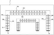
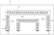
需要说明的是,参考图30-图41,大体U形的感应本体20包括第一至第三本体部201、202、203。第一至第三本体部201、202、203可以均为矩形。为了显示清楚,以大体U形感应本体20的第一本体部201、第二本体部202竖直延伸且第三本体部203水平延伸而为例进行说明,也就是说,第一本体部201、第二本体部202的延伸方向为图30-41中的上下方向,而与延伸方向正交的方向为图中的左右方向。第三本体部203的延伸方向为图30-41中的左右方向,而与延伸方向正交的方向为图中的上下方向。It should be noted that referring to FIGS. 30-41 , the generally
其中图30-34中示出的是电流通路部25以曲线方式延伸在大体U形的感应本体20的第一和第二端之间以便在电流通路部25的延伸方向上电流通路部25的长度L大于感应本体20的长度。由此增加了R=P*L/h公式中的L,进而使得第一电极21和第二电极22之间的电阻R变大,由此提高了感应的线性度。30-34 shows that the
图35-38示出的是电流通路部25以曲线方式延伸在第一和第二端之间以便在电流通路部25的延伸方向上电流通路部25的长度L大于感应本体20的长度,且电流通路部25延伸在第一端和第二端之间且在正交于其延伸方向的平面上的截面积小于感应本体20在平面上的截面积,使得电流通路部25的路径更长且宽度减小。由此在R=P*L/h公式中增加了L且减小了h,进而使得第一电极21和第二电极22之间的电阻R变大,由此提高了感应的线性度。35-38 show that the
图39-图41示出的是电流通路部25为两个,其中一个电流通路部25邻近感应本体20的沿延伸方向延伸的一个侧边,另一个电流通路部25邻近感应本体20的沿延伸方向延伸的另一个侧边。由此使得电流通路部25的路径更长且宽度减小,也就是在R=P*L/h公式中增加了长度L同时减小了宽度h,从而增加了第一电极21和第二电极22之间的电阻R,由此提高了感应的线性度。39-41 show that there are two
本发明实施例中的触摸检测组件100中采用大体U形感应本体20,不仅结构简单,便于制作,所有引线都在同一边,设计方便,减少银浆成本且可减少生产成本。The
在本发明的一些实施例中,触摸检测组件100内可包括多个L形感应单元或大体U形感应单元2,即包括多个L形感应本体或大体U形感应门体20,如图42和图43所示,每个感应门体20的长度不同,多个感应门体20之间相互嵌套。在本发明的实施例中,所谓相互嵌套是指外围绕的感应本体相应地包围内侧的感应本体,这样能够在保证精度的同时达到较大的覆盖率,并且降低运算的复杂度,提高触摸检测组件的响应速度。当然本领域技术人员还可根据图42和图43的思想采用其他相互嵌套的方式排列感应本体。In some embodiments of the present invention, the
可选地,相邻两个感应单元2之间的间距相等,这样就可以通过多个感应单元2对触摸检测组件的两边的均匀划分,从而提高运算速度,提高计算速度,如图42所示。Optionally, the spacing between two
当然在本发明的另一个实施例中,相邻两个感应单元2之间的间距也可以不等,如图43所示,例如由于用户往往触摸在触摸检测组件100的中心部位,因此可以将触摸检测组件100中心部位的感应单元2之间的间距减小,从而提高中心部位的检测精度。Of course, in another embodiment of the present invention, the distance between two
需要说明的是,上述L形感应本体或大体U形感应门体20为本发明较优的实施例,其能够获得较大的覆盖率,但是本发明的其他实施例可对图42和图43进行一些等同的变化,例如大体U形感应门体20中的第一本体部201和第二本体部202可以是不平行的。It should be noted that the above-mentioned L-shaped sensing body or substantially U-shaped
本发明实施例的触摸检测组件100中的感应单元2采用双端检测,即感应单元2的两端均具有电极,且每个电极均与控制芯片200的对应管脚相连,在进行触摸检测时通过感应单元2自身即可实现对触摸点的定位。The
有利地,本发明的实施例通过计算第一电阻R1和第二电阻R2之间比例实现触摸位置的确定,因此相对于目前的菱形或三角形设计来说,由于在确定触摸位置时,无需计算自电容的大小,且自电容的大小不会影响触摸位置的精度,对自电容检测精度的依赖降低,从而提高了测量精度,改善了线性度。此外,由于本发明实施例的第一至第三本体部中任意一个均可为形状规则的矩形,因此相对于目前的菱形或三角形等不规则的形状来说,也可以进一步地提高线性度。Advantageously, the embodiment of the present invention realizes the determination of the touch position by calculating the ratio between the first resistor R1 and the second resistor R2. Therefore, compared with the current rhombus or triangle design, there is no need to calculate the touch position when determining the touch position. The size of the capacitance, and the size of the self-capacitance will not affect the accuracy of the touch position, and the dependence on the detection accuracy of the self-capacitance is reduced, thereby improving the measurement accuracy and improving the linearity. In addition, since any one of the first to third body parts in the embodiment of the present invention can be a regular rectangle, the linearity can be further improved compared to the current irregular shapes such as rhombus or triangle.
本领域技术人员可以理解,对于感应单元2来说,只要感应本体20的长度满足触摸检测组件要求,且两端电极分别与控制芯片200的不同的管脚相连以能够对感应单元进行充电和放电即可,因此可以看出本发明并不限制感应单元的具体结构。感应单元可以有多种结构,本领域技术人员可在本发明上述思想的基础上对感应单元进行变化或者改进,但是只要未脱离本发明的上述思想这些结构就应包含在本发明的范围之内。Those skilled in the art can understand that for the
图44为本发明实施例的触摸检测组件100中大体U形感应单元被触摸时的示意图。从图44可知,第一电极为21,第二电极为22,触摸位置接近于第二电极22,假设感应单元2的长度为10个单位长度,且将感应单元2均匀地分为10份,其中,感应单元2的第三本体部203的长度为4个单位长度,第一本体部201和第二本体部202的长度为3个单位长度。经过检测,获知第一电阻和第二电阻之比为4∶1,即第一电极21至触摸位置的长度(由第一电阻R1体现)为全部感应单元长度的80%。换句话说,触摸点位于距离第一电极21处8个单位长度的位置,获知,触摸点位于距离第二电极22处2个单位长度的位置。当手指移动时,触摸位置会相应移动,因此通过触摸位置的变换就可判断手指相应的移动轨迹,从而判断用户的输入指令。FIG. 44 is a schematic diagram of a substantially U-shaped sensing unit in the
从图44的以上例子可以看出,根据本发明实施例的触摸检测组件的计算方式非常简单,因此能够极大地提高触摸检测组件100检测的反应速度。It can be seen from the above example in FIG. 44 that the calculation method of the touch detection component according to the embodiment of the present invention is very simple, so the reaction speed of the
图45为本发明实施例的触摸检测组件100中L形感应单元被触摸时的示意图。从图45可知,第一电极为21,第二电极为22,触摸位置接近于第二电极22,假设感应本体20的长度为10个单位长度,且将感应本体均匀地分为10份,其中,第一本体部201的长度为5个单位长度,第二本体部202的长度为5个单位长度。经过检测,获知第一电阻R1和第二电阻R2之比为9∶1,即第一电极21至触摸位置的长度(由第一电阻R1体现)为全部感应单元长度的90%。换句话说,触摸点位于距离第一电极21处9个单位长度的位置,获知,触摸点位于距离第二电极22处1个单位长度的位置。FIG. 45 is a schematic diagram when the L-shaped sensing unit in the
从图45中可以看出,根据本发明实施例的触摸检测组件的计算方式非常简单,因此能够极大地提高触摸检测组件检测的反应速度。It can be seen from FIG. 45 that the calculation method of the touch detection component according to the embodiment of the present invention is very simple, so the reaction speed of the touch detection component can be greatly improved.
综上所述,根据本发明实施例的触控装置,通过对感应单元2两端的电极21、22施加电平信号,如果该感应单元2被触碰,则该感应单元2会形成自电容,因此通过施加的电平信号可对该自电容进行充电,并根据第一电阻R1和第二电阻R2之间的比例关系确定在第一方向上的触摸位置。例如在本发明的一个实施例中,第一电阻和第二电阻之间的比例关系根据在对所述自电容充电/放电时,从所述第一电极和/或第二电极进行检测获得的第一检测值和第二检测值之间的比例关系计算得到。因此从第一电极和/或第二电极检测该自电容充电/放电时产生的第一检测值和第二检测值。这样,通过第一检测值和第二检测值就能够反应触摸点位于该感应单元的位置,从而进一步确定触摸点在触摸检测组件的位置。To sum up, according to the touch device of the embodiment of the present invention, by applying a level signal to the
根据本发明实施例的便携式电子设备可以包括参考上述实施例描述的触摸检测组件100。根据本发明实施例的便携式电子设备可以包括参考上述实施例描述的的触控装置。根据本发明实施例的便携式电子设备的其他构成例如框架结构和控制组成等以及操作对于本领域普通技术人员而言都是已知的,这里不再详细描述。A portable electronic device according to an embodiment of the present invention may include the
在本说明书的描述中,参考术语“一个实施例”、“一些实施例”、“示意性实施例”、“示例”、“具体示例”、或“一些示例”等的描述意指结合该实施例或示例描述的具体特征、结构、材料或者特点包含于本发明的至少一个实施例或示例中。在本说明书中,对上述术语的示意性表述不一定指的是相同的实施例或示例。而且,描述的具体特征、结构、材料或者特点可以在任何的一个或多个实施例或示例中以合适的方式结合。In the description of this specification, references to the terms "one embodiment," "some embodiments," "exemplary embodiments," "example," "specific examples," or "some examples" are intended to mean that the implementation A specific feature, structure, material, or characteristic described by an embodiment or example is included in at least one embodiment or example of the present invention. In this specification, schematic representations of the above terms do not necessarily refer to the same embodiment or example. Furthermore, the specific features, structures, materials or characteristics described may be combined in any suitable manner in any one or more embodiments or examples.
尽管已经示出和描述了本发明的实施例,本领域的普通技术人员可以理解:在不脱离本发明的原理和宗旨的情况下可以对这些实施例进行多种变化、修改、替换和变型,本发明的范围由权利要求及其等同物限定。Although the embodiments of the present invention have been shown and described, those skilled in the art can understand that various changes, modifications, substitutions and modifications can be made to these embodiments without departing from the principle and spirit of the present invention. The scope of the invention is defined by the claims and their equivalents.
Claims (22)
Translated fromChinesePriority Applications (1)
| Application Number | Priority Date | Filing Date | Title |
|---|---|---|---|
| CN201210093681.1ACN102902443B (en) | 2011-07-26 | 2012-04-01 | A kind of touch detection components, contactor control device and portable electric appts |
Applications Claiming Priority (5)
| Application Number | Priority Date | Filing Date | Title |
|---|---|---|---|
| CN201110210959 | 2011-07-26 | ||
| CN201110211018.2 | 2011-07-26 | ||
| CN201110211018 | 2011-07-26 | ||
| CN201110210959.4 | 2011-07-26 | ||
| CN201210093681.1ACN102902443B (en) | 2011-07-26 | 2012-04-01 | A kind of touch detection components, contactor control device and portable electric appts |
Publications (2)
| Publication Number | Publication Date |
|---|---|
| CN102902443Atrue CN102902443A (en) | 2013-01-30 |
| CN102902443B CN102902443B (en) | 2016-01-13 |
Family
ID=47169405
Family Applications (40)
| Application Number | Title | Priority Date | Filing Date |
|---|---|---|---|
| CN2011205738057UExpired - LifetimeCN202795313U (en) | 2011-07-26 | 2011-12-31 | Touch control device and portable electronic device |
| CN2011205736297UExpired - LifetimeCN202600660U (en) | 2011-07-26 | 2011-12-31 | Touch control device and portable electronic equipment |
| CN201110459293.6AExpired - Fee RelatedCN102902429B (en) | 2011-07-26 | 2011-12-31 | Touch detecting method and contactor control device |
| CN201110459408.1AExpired - Fee RelatedCN102902435B (en) | 2011-07-26 | 2011-12-31 | Touch detecting method and contactor control device |
| CN201110459295.5AExpired - Fee RelatedCN102902430B (en) | 2011-07-26 | 2011-12-31 | Touch detecting method and contactor control device |
| CN2011205738593UExpired - LifetimeCN202795285U (en) | 2011-07-26 | 2011-12-31 | Touch control device and portable electronic device |
| CN201110459466.4AExpired - Fee RelatedCN102902437B (en) | 2011-07-26 | 2011-12-31 | Touch-screen testing equipment and contactor control device |
| CN2011205737694UExpired - LifetimeCN202548807U (en) | 2011-07-26 | 2011-12-31 | Touch control device and portable electronic equipment |
| CN2011205737919UExpired - LifetimeCN202649984U (en) | 2011-07-26 | 2011-12-31 | Touch screen detection device, touch control device, and portable electronic device |
| CN201110459486.1AExpired - Fee RelatedCN102902440B (en) | 2011-07-26 | 2011-12-31 | Touch detecting method and contactor control device |
| CN201110459482.3AExpired - Fee RelatedCN102902439B (en) | 2011-07-26 | 2011-12-31 | Touch detection method and touch device |
| CN2011205734658UExpired - LifetimeCN202548805U (en) | 2011-07-26 | 2011-12-31 | Touch screen detection equipment, touch device and portable electronic equipment |
| CN2011205737976UExpired - LifetimeCN202600661U (en) | 2011-07-26 | 2011-12-31 | Touch screen detection equipment, touch control device and portable electronic equipment |
| CN201110459316.3AExpired - Fee RelatedCN102902432B (en) | 2011-07-26 | 2011-12-31 | Touch detecting method and contactor control device |
| CN201110459333.7AActiveCN102902433B (en) | 2011-07-26 | 2011-12-31 | Touch detection method and touch control device |
| CN201110459313.XAExpired - Fee RelatedCN102902431B (en) | 2011-07-26 | 2011-12-31 | Touch detecting method and contactor control device |
| CN2011205736916UExpired - LifetimeCN202548806U (en) | 2011-07-26 | 2011-12-31 | Touch control apparatus and portable electronic equipment |
| CN201110459367.6AExpired - Fee RelatedCN102902434B (en) | 2011-07-26 | 2011-12-31 | Touch detecting method and contactor control device |
| CN201110459292.1AExpired - Fee RelatedCN102902428B (en) | 2011-07-26 | 2011-12-31 | Touch detecting method and contactor control device |
| CN201110459449.0AExpired - Fee RelatedCN102902436B (en) | 2011-07-26 | 2011-12-31 | Touch screen detection equipment and touch device |
| CN201110459473.4AExpired - Fee RelatedCN102902438B (en) | 2011-07-26 | 2011-12-31 | Touch detecting method, touch screen detection device and contactor control device |
| CN2011205734681UExpired - LifetimeCN202795312U (en) | 2011-07-26 | 2011-12-31 | Touch control device and portable electronic device |
| CN2011205734304UExpired - LifetimeCN202795311U (en) | 2011-07-26 | 2011-12-31 | Touch control device and portable electronic device |
| CN201110459115.3AExpired - Fee RelatedCN102902427B (en) | 2011-07-26 | 2011-12-31 | Touch detecting method and contactor control device |
| CN201120573486XUExpired - LifetimeCN202649983U (en) | 2011-07-26 | 2011-12-31 | Touch control device and portable electronic device |
| CN2011205733797UExpired - LifetimeCN202795310U (en) | 2011-07-26 | 2011-12-31 | Touch control device and portable electronic device |
| CN2011205732173UExpired - LifetimeCN202548804U (en) | 2011-07-26 | 2011-12-31 | Touch device and portable electronic device |
| CN2011205732224UExpired - LifetimeCN202795309U (en) | 2011-07-26 | 2011-12-31 | Touch control device and portable electronic device |
| CN2012201340878UExpired - LifetimeCN202649961U (en) | 2011-07-26 | 2012-04-01 | Touch detection assembly, touch control device and portable electric equipment |
| CN2012201345443UExpired - LifetimeCN202615359U (en) | 2011-07-26 | 2012-04-01 | Touch detection module and touch control device and portable electronic equipment |
| CN2012201340971UExpired - LifetimeCN202795314U (en) | 2011-07-26 | 2012-04-01 | Touch control device and touch detecting assembly thereof and portable electronic device |
| CN201210093658.2AExpired - Fee RelatedCN102902442B (en) | 2011-07-26 | 2012-04-01 | Touch detection components, contactor control device and portable electric appts |
| CN2012201345316UExpired - LifetimeCN202795315U (en) | 2011-07-26 | 2012-04-01 | Touching detection assembly and touching control device and portable type electronic device |
| CN201210093681.1AExpired - Fee RelatedCN102902443B (en) | 2011-07-26 | 2012-04-01 | A kind of touch detection components, contactor control device and portable electric appts |
| CN201210093687.9AExpired - Fee RelatedCN102902399B (en) | 2011-07-26 | 2012-04-01 | Touch detection components, contactor control device and a kind of portable electric appts |
| CN201210094078.5AExpired - Fee RelatedCN102902444B (en) | 2011-07-26 | 2012-04-01 | Touch detection components, a kind of contactor control device and portable electric appts |
| CN201210093646.XAExpired - Fee RelatedCN102902398B (en) | 2011-07-26 | 2012-04-01 | Portable electric appts, touch detection components and contactor control device |
| CN201220134083XUExpired - LifetimeCN202649960U (en) | 2011-07-26 | 2012-04-01 | Portable electric equipment, touch detection assembly and touch control device |
| CN201210093649.3AExpired - Fee RelatedCN102902441B (en) | 2011-07-26 | 2012-04-01 | Touch detection components, contactor control device and portable electric appts |
| CN2012201341090UExpired - LifetimeCN202870787U (en) | 2011-07-26 | 2012-04-01 | Touch detection component, touch control device and portable electronic equipment |
Family Applications Before (33)
| Application Number | Title | Priority Date | Filing Date |
|---|---|---|---|
| CN2011205738057UExpired - LifetimeCN202795313U (en) | 2011-07-26 | 2011-12-31 | Touch control device and portable electronic device |
| CN2011205736297UExpired - LifetimeCN202600660U (en) | 2011-07-26 | 2011-12-31 | Touch control device and portable electronic equipment |
| CN201110459293.6AExpired - Fee RelatedCN102902429B (en) | 2011-07-26 | 2011-12-31 | Touch detecting method and contactor control device |
| CN201110459408.1AExpired - Fee RelatedCN102902435B (en) | 2011-07-26 | 2011-12-31 | Touch detecting method and contactor control device |
| CN201110459295.5AExpired - Fee RelatedCN102902430B (en) | 2011-07-26 | 2011-12-31 | Touch detecting method and contactor control device |
| CN2011205738593UExpired - LifetimeCN202795285U (en) | 2011-07-26 | 2011-12-31 | Touch control device and portable electronic device |
| CN201110459466.4AExpired - Fee RelatedCN102902437B (en) | 2011-07-26 | 2011-12-31 | Touch-screen testing equipment and contactor control device |
| CN2011205737694UExpired - LifetimeCN202548807U (en) | 2011-07-26 | 2011-12-31 | Touch control device and portable electronic equipment |
| CN2011205737919UExpired - LifetimeCN202649984U (en) | 2011-07-26 | 2011-12-31 | Touch screen detection device, touch control device, and portable electronic device |
| CN201110459486.1AExpired - Fee RelatedCN102902440B (en) | 2011-07-26 | 2011-12-31 | Touch detecting method and contactor control device |
| CN201110459482.3AExpired - Fee RelatedCN102902439B (en) | 2011-07-26 | 2011-12-31 | Touch detection method and touch device |
| CN2011205734658UExpired - LifetimeCN202548805U (en) | 2011-07-26 | 2011-12-31 | Touch screen detection equipment, touch device and portable electronic equipment |
| CN2011205737976UExpired - LifetimeCN202600661U (en) | 2011-07-26 | 2011-12-31 | Touch screen detection equipment, touch control device and portable electronic equipment |
| CN201110459316.3AExpired - Fee RelatedCN102902432B (en) | 2011-07-26 | 2011-12-31 | Touch detecting method and contactor control device |
| CN201110459333.7AActiveCN102902433B (en) | 2011-07-26 | 2011-12-31 | Touch detection method and touch control device |
| CN201110459313.XAExpired - Fee RelatedCN102902431B (en) | 2011-07-26 | 2011-12-31 | Touch detecting method and contactor control device |
| CN2011205736916UExpired - LifetimeCN202548806U (en) | 2011-07-26 | 2011-12-31 | Touch control apparatus and portable electronic equipment |
| CN201110459367.6AExpired - Fee RelatedCN102902434B (en) | 2011-07-26 | 2011-12-31 | Touch detecting method and contactor control device |
| CN201110459292.1AExpired - Fee RelatedCN102902428B (en) | 2011-07-26 | 2011-12-31 | Touch detecting method and contactor control device |
| CN201110459449.0AExpired - Fee RelatedCN102902436B (en) | 2011-07-26 | 2011-12-31 | Touch screen detection equipment and touch device |
| CN201110459473.4AExpired - Fee RelatedCN102902438B (en) | 2011-07-26 | 2011-12-31 | Touch detecting method, touch screen detection device and contactor control device |
| CN2011205734681UExpired - LifetimeCN202795312U (en) | 2011-07-26 | 2011-12-31 | Touch control device and portable electronic device |
| CN2011205734304UExpired - LifetimeCN202795311U (en) | 2011-07-26 | 2011-12-31 | Touch control device and portable electronic device |
| CN201110459115.3AExpired - Fee RelatedCN102902427B (en) | 2011-07-26 | 2011-12-31 | Touch detecting method and contactor control device |
| CN201120573486XUExpired - LifetimeCN202649983U (en) | 2011-07-26 | 2011-12-31 | Touch control device and portable electronic device |
| CN2011205733797UExpired - LifetimeCN202795310U (en) | 2011-07-26 | 2011-12-31 | Touch control device and portable electronic device |
| CN2011205732173UExpired - LifetimeCN202548804U (en) | 2011-07-26 | 2011-12-31 | Touch device and portable electronic device |
| CN2011205732224UExpired - LifetimeCN202795309U (en) | 2011-07-26 | 2011-12-31 | Touch control device and portable electronic device |
| CN2012201340878UExpired - LifetimeCN202649961U (en) | 2011-07-26 | 2012-04-01 | Touch detection assembly, touch control device and portable electric equipment |
| CN2012201345443UExpired - LifetimeCN202615359U (en) | 2011-07-26 | 2012-04-01 | Touch detection module and touch control device and portable electronic equipment |
| CN2012201340971UExpired - LifetimeCN202795314U (en) | 2011-07-26 | 2012-04-01 | Touch control device and touch detecting assembly thereof and portable electronic device |
| CN201210093658.2AExpired - Fee RelatedCN102902442B (en) | 2011-07-26 | 2012-04-01 | Touch detection components, contactor control device and portable electric appts |
| CN2012201345316UExpired - LifetimeCN202795315U (en) | 2011-07-26 | 2012-04-01 | Touching detection assembly and touching control device and portable type electronic device |
Family Applications After (6)
| Application Number | Title | Priority Date | Filing Date |
|---|---|---|---|
| CN201210093687.9AExpired - Fee RelatedCN102902399B (en) | 2011-07-26 | 2012-04-01 | Touch detection components, contactor control device and a kind of portable electric appts |
| CN201210094078.5AExpired - Fee RelatedCN102902444B (en) | 2011-07-26 | 2012-04-01 | Touch detection components, a kind of contactor control device and portable electric appts |
| CN201210093646.XAExpired - Fee RelatedCN102902398B (en) | 2011-07-26 | 2012-04-01 | Portable electric appts, touch detection components and contactor control device |
| CN201220134083XUExpired - LifetimeCN202649960U (en) | 2011-07-26 | 2012-04-01 | Portable electric equipment, touch detection assembly and touch control device |
| CN201210093649.3AExpired - Fee RelatedCN102902441B (en) | 2011-07-26 | 2012-04-01 | Touch detection components, contactor control device and portable electric appts |
| CN2012201341090UExpired - LifetimeCN202870787U (en) | 2011-07-26 | 2012-04-01 | Touch detection component, touch control device and portable electronic equipment |
Country Status (3)
| Country | Link |
|---|---|
| CN (40) | CN202795313U (en) |
| TW (14) | TWM449305U (en) |
| WO (7) | WO2013013624A1 (en) |
Cited By (1)
| Publication number | Priority date | Publication date | Assignee | Title |
|---|---|---|---|---|
| TWI610203B (en)* | 2014-02-14 | 2018-01-01 | 晨星半導體股份有限公司 | Electrode of self-capacitive touch panel utilizing serpentine trace to increase resistance and self-capacitive touch panel |
Families Citing this family (29)
| Publication number | Priority date | Publication date | Assignee | Title |
|---|---|---|---|---|
| CN202795313U (en)* | 2011-07-26 | 2013-03-13 | 比亚迪股份有限公司 | Touch control device and portable electronic device |
| CN103105988B (en)* | 2013-01-22 | 2016-01-06 | 北京京东方光电科技有限公司 | Capacitive touch screen, the manufacture method of touch control display apparatus and capacitive touch screen |
| CN103294319A (en)* | 2013-06-06 | 2013-09-11 | 敦泰科技有限公司 | Capacitive touch screen |
| TWI502460B (en)* | 2013-08-07 | 2015-10-01 | Focaltech Electronics Ltd | A self-capacitive touch screen and a touch control apparatus |
| US9552089B2 (en) | 2013-08-07 | 2017-01-24 | Synaptics Incorporated | Capacitive sensing using a matrix electrode pattern |
| CN103455228B (en)* | 2013-08-30 | 2016-10-19 | 珠海中慧微电子有限公司 | Automatically induction point and the method for capacitance touch screen driving voltage load time are calculated |
| WO2015058350A1 (en)* | 2013-10-22 | 2015-04-30 | 敦泰科技有限公司 | Self-capacitance change detection method and self-capacitance sensing device for touch screen |
| CN103699278B (en)* | 2013-10-22 | 2017-01-11 | 敦泰电子有限公司 | Self-capacitance change detection method and self-capacitance sensing device for touch screen |
| TWI515634B (en)* | 2013-11-08 | 2016-01-01 | 義隆電子股份有限公司 | Touch device and sensing method for of the touch device |
| JP6216252B2 (en)* | 2014-01-09 | 2017-10-18 | アルプス電気株式会社 | Input device |
| CN104808870A (en)* | 2014-01-23 | 2015-07-29 | 天津富纳源创科技有限公司 | Detection method of touch point of single-layer capacitive touch screen |
| CN104850283B (en)* | 2014-02-14 | 2018-02-02 | 晨星半导体股份有限公司 | Self-capacitance touch panel electrode using zigzag line segment to increase resistance value |
| US9703431B2 (en) | 2014-06-03 | 2017-07-11 | Synaptics Incorporated | Noise detection and mitigation for capacitive sensing devices |
| US9753587B2 (en) | 2014-06-05 | 2017-09-05 | Synaptics Incorporated | Driving sensor electrodes for absolute capacitive sensing |
| US9703430B2 (en) | 2014-06-30 | 2017-07-11 | Synaptics Incorporated | Driving sensor electrodes for proximity sensing |
| US9746975B2 (en) | 2015-03-27 | 2017-08-29 | Synaptics Incorporated | Capacitive measurement processing for mode changes |
| WO2016183440A1 (en) | 2015-05-13 | 2016-11-17 | Lukla Llc | Garment with strategically positioned polymide aerogel panels |
| CN106325578B (en)* | 2015-07-10 | 2023-07-25 | 宸鸿科技(厦门)有限公司 | Pressure sensitive touch panel |
| CN107294521B (en)* | 2016-03-31 | 2020-08-21 | 日本电气株式会社 | Induction detection method and device |
| CN106527451B (en)* | 2016-12-27 | 2023-07-11 | 许筠 | On-screen interactive robot |
| CN107328555A (en)* | 2017-06-20 | 2017-11-07 | 合肥市惠科精密模具有限公司 | A kind of display screen foreign matter detecting method |
| CN108108055B (en)* | 2018-01-02 | 2021-11-16 | 联想(北京)有限公司 | Touch device, touch method and electronic equipment |
| CN109375839B (en)* | 2018-12-03 | 2020-06-30 | 武汉华星光电半导体显示技术有限公司 | Touch screen and display device |
| TWI724790B (en)* | 2020-02-14 | 2021-04-11 | 李尚禮 | Resistive touch device and resistive touch-sensing method |
| TWI727662B (en)* | 2020-02-14 | 2021-05-11 | 李尚禮 | Resistive touch device and resistive touch-sensing method |
| CN111762023B (en)* | 2020-05-29 | 2022-04-12 | 法雷奥舒适驾驶辅助系统(广州)有限公司 | Touch device and method thereof and auxiliary switch of automobile steering wheel |
| CN111766978B (en)* | 2020-06-12 | 2021-09-24 | 深圳市华星光电半导体显示技术有限公司 | Touch control assembly and touch control display device |
| CN111813277A (en)* | 2020-07-10 | 2020-10-23 | 温州长江汽车电子有限公司 | Double-layer pressure touch signal acquisition method of capacitive touch switch |
| CN114361148A (en)* | 2020-09-30 | 2022-04-15 | Tcl科技集团股份有限公司 | Pixel structure, lamp panel, display device and driving method of pixel structure |
Citations (4)
| Publication number | Priority date | Publication date | Assignee | Title |
|---|---|---|---|---|
| CN201174111Y (en)* | 2008-03-12 | 2008-12-31 | 洋华光电股份有限公司 | Signal conduction structure of touch panel |
| CN101655754A (en)* | 2008-08-21 | 2010-02-24 | 株式会社和冠 | Meshed touchscreen pattern |
| US20100182275A1 (en)* | 2009-01-20 | 2010-07-22 | Hitachi Displays, Ltd. | Display device |
| CN202795315U (en)* | 2011-07-26 | 2013-03-13 | 比亚迪股份有限公司 | Touching detection assembly and touching control device and portable type electronic device |
Family Cites Families (34)
| Publication number | Priority date | Publication date | Assignee | Title |
|---|---|---|---|---|
| JPH1091350A (en)* | 1996-09-10 | 1998-04-10 | Tokyo Cosmos Electric Co Ltd | Touch panel |
| JP3220405B2 (en)* | 1997-02-20 | 2001-10-22 | アルプス電気株式会社 | Coordinate input device |
| US6057903A (en)* | 1998-08-18 | 2000-05-02 | International Business Machines Corporation | Liquid crystal display device employing a guard plane between a layer for measuring touch position and common electrode layer |
| US6297811B1 (en)* | 1999-06-02 | 2001-10-02 | Elo Touchsystems, Inc. | Projective capacitive touchscreen |
| JP2006504948A (en)* | 2002-10-31 | 2006-02-09 | フィリップ、ハラルド | Capacitive position sensor using charge transfer |
| TWI258708B (en)* | 2005-01-27 | 2006-07-21 | Apex Material Technology Corp | Resistive touch panel, and it manufacturing method |
| WO2007091579A1 (en)* | 2006-02-10 | 2007-08-16 | Sharp Kabushiki Kaisha | Touch panel coordinate position detection device |
| GB2439614B (en)* | 2006-05-31 | 2008-12-24 | Harald Philipp | Two-dimensional position sensor |
| TW200844827A (en)* | 2007-05-11 | 2008-11-16 | Sense Pad Tech Co Ltd | Transparent touch panel device |
| KR101530189B1 (en)* | 2007-07-19 | 2015-06-22 | (주)멜파스 | Touchscreen apparatus having multiple bar-type transparent electrodes |
| JP5094376B2 (en)* | 2007-12-28 | 2012-12-12 | 株式会社ワコム | Position detection device |
| TW200935290A (en)* | 2008-01-15 | 2009-08-16 | Ad Semiconductor Co Ltd | Resistive touch screen which can identify multi-touch |
| US8830180B2 (en)* | 2008-04-10 | 2014-09-09 | Atmel Corporation | Capacitive position sensor |
| US8487898B2 (en)* | 2008-04-25 | 2013-07-16 | Apple Inc. | Ground guard for capacitive sensing |
| CN101661356B (en)* | 2008-08-25 | 2011-07-06 | 盛群半导体股份有限公司 | Capacitive charge compensation method for touch sensing device |
| CN101751172A (en)* | 2008-12-08 | 2010-06-23 | 上海天马微电子有限公司 | Touch position detection method and touch screen |
| CN101847066A (en)* | 2009-03-25 | 2010-09-29 | 友达光电股份有限公司 | Mutual capacitance type touch display device |
| JP5193942B2 (en)* | 2009-05-14 | 2013-05-08 | 京セラディスプレイ株式会社 | Capacitive touch panel device |
| TWI543048B (en)* | 2009-05-15 | 2016-07-21 | 晨星半導體股份有限公司 | A sensor structure of a capacitive touch panel and the sensing method thereof |
| TWI528250B (en)* | 2009-06-25 | 2016-04-01 | Elan Microelectronics Corp | Object Detector and Method for Capacitive Touchpad |
| TW201102895A (en)* | 2009-07-10 | 2011-01-16 | Focaltech Systems Ltd | Ultra-thin mutual capacitance touch panel and assembly-type ultra-thin touch panel |
| CN101996014B (en)* | 2009-08-21 | 2013-08-14 | 宏达国际电子股份有限公司 | Pressure detection method of touch sensing element and electronic device using same |
| US9632628B2 (en)* | 2009-10-23 | 2017-04-25 | Atmel Corporation | Interdigitated touchscreen electrodes |
| TWI489356B (en)* | 2009-12-15 | 2015-06-21 | Au Optronics Corp | Touch display device and touch sensing device |
| TWI417777B (en)* | 2009-12-24 | 2013-12-01 | Orise Technology Co Ltd | Capacitive touch panel with high touching sensitivity |
| KR20110076188A (en)* | 2009-12-29 | 2011-07-06 | 삼성전자주식회사 | Capacitive Sensing Device and Manufacturing Method |
| CN101840293B (en)* | 2010-01-21 | 2012-03-21 | 宸鸿科技(厦门)有限公司 | Scanning method for projected capacitive touch panels |
| CN101923419A (en)* | 2010-04-20 | 2010-12-22 | 敦泰科技有限公司 | Self-capacitance touch screen with one-dimensional electrodes and its coordinate data processing method |
| TWI426435B (en)* | 2010-09-14 | 2014-02-11 | Sentelic Corp | Capacitive touch panel and its manufacturing method |
| CN101984391B (en)* | 2010-10-13 | 2012-12-26 | 友达光电股份有限公司 | Touch panel and its repair method |
| TWI426437B (en)* | 2010-10-28 | 2014-02-11 | Young Lighting Technology Inc | Capacitive touch panel |
| TWI421756B (en)* | 2010-12-23 | 2014-01-01 | Au Optronics Corp | Touch display panel and touch sensing panel |
| CN202267944U (en)* | 2011-07-26 | 2012-06-06 | 比亚迪股份有限公司 | Touch screen detecting device and touch control device |
| CN202422046U (en)* | 2011-07-26 | 2012-09-05 | 比亚迪股份有限公司 | Induction unit, touch screen detection device and touch control device |
- 2011
- 2011-12-31CNCN2011205738057Upatent/CN202795313U/ennot_activeExpired - Lifetime
- 2011-12-31CNCN2011205736297Upatent/CN202600660U/ennot_activeExpired - Lifetime
- 2011-12-31CNCN201110459293.6Apatent/CN102902429B/ennot_activeExpired - Fee Related
- 2011-12-31CNCN201110459408.1Apatent/CN102902435B/ennot_activeExpired - Fee Related
- 2011-12-31CNCN201110459295.5Apatent/CN102902430B/ennot_activeExpired - Fee Related
- 2011-12-31CNCN2011205738593Upatent/CN202795285U/ennot_activeExpired - Lifetime
- 2011-12-31CNCN201110459466.4Apatent/CN102902437B/ennot_activeExpired - Fee Related
- 2011-12-31CNCN2011205737694Upatent/CN202548807U/ennot_activeExpired - Lifetime
- 2011-12-31CNCN2011205737919Upatent/CN202649984U/ennot_activeExpired - Lifetime
- 2011-12-31CNCN201110459486.1Apatent/CN102902440B/ennot_activeExpired - Fee Related
- 2011-12-31CNCN201110459482.3Apatent/CN102902439B/ennot_activeExpired - Fee Related
- 2011-12-31CNCN2011205734658Upatent/CN202548805U/ennot_activeExpired - Lifetime
- 2011-12-31CNCN2011205737976Upatent/CN202600661U/ennot_activeExpired - Lifetime
- 2011-12-31CNCN201110459316.3Apatent/CN102902432B/ennot_activeExpired - Fee Related
- 2011-12-31CNCN201110459333.7Apatent/CN102902433B/enactiveActive
- 2011-12-31CNCN201110459313.XApatent/CN102902431B/ennot_activeExpired - Fee Related
- 2011-12-31CNCN2011205736916Upatent/CN202548806U/ennot_activeExpired - Lifetime
- 2011-12-31CNCN201110459367.6Apatent/CN102902434B/ennot_activeExpired - Fee Related
- 2011-12-31CNCN201110459292.1Apatent/CN102902428B/ennot_activeExpired - Fee Related
- 2011-12-31CNCN201110459449.0Apatent/CN102902436B/ennot_activeExpired - Fee Related
- 2011-12-31CNCN201110459473.4Apatent/CN102902438B/ennot_activeExpired - Fee Related
- 2011-12-31CNCN2011205734681Upatent/CN202795312U/ennot_activeExpired - Lifetime
- 2011-12-31CNCN2011205734304Upatent/CN202795311U/ennot_activeExpired - Lifetime
- 2011-12-31CNCN201110459115.3Apatent/CN102902427B/ennot_activeExpired - Fee Related
- 2011-12-31CNCN201120573486XUpatent/CN202649983U/ennot_activeExpired - Lifetime
- 2011-12-31CNCN2011205733797Upatent/CN202795310U/ennot_activeExpired - Lifetime
- 2011-12-31CNCN2011205732173Upatent/CN202548804U/ennot_activeExpired - Lifetime
- 2011-12-31CNCN2011205732224Upatent/CN202795309U/ennot_activeExpired - Lifetime
- 2012
- 2012-04-01CNCN2012201340878Upatent/CN202649961U/ennot_activeExpired - Lifetime
- 2012-04-01CNCN2012201345443Upatent/CN202615359U/ennot_activeExpired - Lifetime
- 2012-04-01CNCN2012201340971Upatent/CN202795314U/ennot_activeExpired - Lifetime
- 2012-04-01CNCN201210093658.2Apatent/CN102902442B/ennot_activeExpired - Fee Related
- 2012-04-01CNCN2012201345316Upatent/CN202795315U/ennot_activeExpired - Lifetime
- 2012-04-01CNCN201210093681.1Apatent/CN102902443B/ennot_activeExpired - Fee Related
- 2012-04-01CNCN201210093687.9Apatent/CN102902399B/ennot_activeExpired - Fee Related
- 2012-04-01CNCN201210094078.5Apatent/CN102902444B/ennot_activeExpired - Fee Related
- 2012-04-01CNCN201210093646.XApatent/CN102902398B/ennot_activeExpired - Fee Related
- 2012-04-01CNCN201220134083XUpatent/CN202649960U/ennot_activeExpired - Lifetime
- 2012-04-01CNCN201210093649.3Apatent/CN102902441B/ennot_activeExpired - Fee Related
- 2012-04-01CNCN2012201341090Upatent/CN202870787U/ennot_activeExpired - Lifetime
- 2012-07-17TWTW101213750Upatent/TWM449305U/ennot_activeIP Right Cessation
- 2012-07-17TWTW101125694Apatent/TWI475437B/ennot_activeIP Right Cessation
- 2012-07-18TWTW101125838Apatent/TWI479399B/ennot_activeIP Right Cessation
- 2012-07-18TWTW101213834Upatent/TWM464745U/enunknown
- 2012-07-18TWTW101125832Apatent/TWI483164B/ennot_activeIP Right Cessation
- 2012-07-18TWTW101213854Upatent/TWM450007U/enunknown
- 2012-07-18TWTW101125847Apatent/TWI494833B/ennot_activeIP Right Cessation
- 2012-07-18TWTW101213838Upatent/TWM457238U/enunknown
- 2012-07-23TWTW101126427Apatent/TWI486848B/ennot_activeIP Right Cessation
- 2012-07-23TWTW101214182Upatent/TWM451595U/enunknown
- 2012-07-26TWTW101126936Apatent/TWI482074B/ennot_activeIP Right Cessation
- 2012-07-26WOPCT/CN2012/079182patent/WO2013013624A1/enactiveApplication Filing
- 2012-07-26TWTW101126935Apatent/TWI485604B/ennot_activeIP Right Cessation
- 2012-07-26WOPCT/CN2012/079220patent/WO2013013634A1/enactiveApplication Filing
- 2012-07-26TWTW101214479Upatent/TWM453897U/enunknown
- 2012-07-26WOPCT/CN2012/079221patent/WO2013013635A1/enactiveApplication Filing
- 2012-07-26WOPCT/CN2012/079186patent/WO2013013625A1/enactiveApplication Filing
- 2012-07-26WOPCT/CN2012/079192patent/WO2013013627A1/enactiveApplication Filing
- 2012-07-26WOPCT/CN2012/079224patent/WO2013013637A1/enactiveApplication Filing
- 2012-07-26TWTW101214478Upatent/TWM470979U/enunknown
- 2012-07-26WOPCT/CN2012/079223patent/WO2013013636A1/enactiveApplication Filing
Patent Citations (4)
| Publication number | Priority date | Publication date | Assignee | Title |
|---|---|---|---|---|
| CN201174111Y (en)* | 2008-03-12 | 2008-12-31 | 洋华光电股份有限公司 | Signal conduction structure of touch panel |
| CN101655754A (en)* | 2008-08-21 | 2010-02-24 | 株式会社和冠 | Meshed touchscreen pattern |
| US20100182275A1 (en)* | 2009-01-20 | 2010-07-22 | Hitachi Displays, Ltd. | Display device |
| CN202795315U (en)* | 2011-07-26 | 2013-03-13 | 比亚迪股份有限公司 | Touching detection assembly and touching control device and portable type electronic device |
Cited By (1)
| Publication number | Priority date | Publication date | Assignee | Title |
|---|---|---|---|---|
| TWI610203B (en)* | 2014-02-14 | 2018-01-01 | 晨星半導體股份有限公司 | Electrode of self-capacitive touch panel utilizing serpentine trace to increase resistance and self-capacitive touch panel |
Also Published As
Similar Documents
| Publication | Publication Date | Title |
|---|---|---|
| CN102902443B (en) | A kind of touch detection components, contactor control device and portable electric appts |
Legal Events
| Date | Code | Title | Description |
|---|---|---|---|
| C06 | Publication | ||
| PB01 | Publication | ||
| C10 | Entry into substantive examination | ||
| SE01 | Entry into force of request for substantive examination | ||
| C14 | Grant of patent or utility model | ||
| GR01 | Patent grant | ||
| TR01 | Transfer of patent right | ||
| TR01 | Transfer of patent right | Effective date of registration:20191227 Address after:518119 1 Yanan Road, Kwai Chung street, Dapeng New District, Shenzhen, Guangdong Patentee after:SHENZHEN BYD MICROELECTRONICS Co.,Ltd. Address before:BYD 518118 Shenzhen Road, Guangdong province Pingshan New District No. 3009 Patentee before:BYD Co.,Ltd. | |
| CP01 | Change in the name or title of a patent holder | ||
| CP01 | Change in the name or title of a patent holder | Address after:518119 No.1 Yan'an Road, Kuiyong street, Dapeng New District, Shenzhen City, Guangdong Province Patentee after:BYD Semiconductor Co.,Ltd. Address before:518119 No.1 Yan'an Road, Kuiyong street, Dapeng New District, Shenzhen City, Guangdong Province Patentee before:SHENZHEN BYD MICROELECTRONICS Co.,Ltd. Address after:518119 No.1 Yan'an Road, Kuiyong street, Dapeng New District, Shenzhen City, Guangdong Province Patentee after:BYD Semiconductor Co.,Ltd. Address before:518119 No.1 Yan'an Road, Kuiyong street, Dapeng New District, Shenzhen City, Guangdong Province Patentee before:BYD Semiconductor Co.,Ltd. | |
| CF01 | Termination of patent right due to non-payment of annual fee | ||
| CF01 | Termination of patent right due to non-payment of annual fee | Granted publication date:20160113 |