CN102893282A - Method and apparatus for performing asynchronous and synchronous reset removal during synthesis - Google Patents
Method and apparatus for performing asynchronous and synchronous reset removal during synthesisDownload PDFInfo
- Publication number
- CN102893282A CN102893282ACN2011800234776ACN201180023477ACN102893282ACN 102893282 ACN102893282 ACN 102893282ACN 2011800234776 ACN2011800234776 ACN 2011800234776ACN 201180023477 ACN201180023477 ACN 201180023477ACN 102893282 ACN102893282 ACN 102893282A
- Authority
- CN
- China
- Prior art keywords
- reset
- register
- redundant
- registers
- identifying
- Prior art date
- Legal status (The legal status is an assumption and is not a legal conclusion. Google has not performed a legal analysis and makes no representation as to the accuracy of the status listed.)
- Granted
Links
Images


Classifications
- G—PHYSICS
- G06—COMPUTING OR CALCULATING; COUNTING
- G06F—ELECTRIC DIGITAL DATA PROCESSING
- G06F30/00—Computer-aided design [CAD]
- G06F30/30—Circuit design
- G06F30/32—Circuit design at the digital level
- G06F30/327—Logic synthesis; Behaviour synthesis, e.g. mapping logic, HDL to netlist, high-level language to RTL or netlist
Landscapes
- Engineering & Computer Science (AREA)
- Computer Hardware Design (AREA)
- Physics & Mathematics (AREA)
- Theoretical Computer Science (AREA)
- Evolutionary Computation (AREA)
- Geometry (AREA)
- General Engineering & Computer Science (AREA)
- General Physics & Mathematics (AREA)
- Design And Manufacture Of Integrated Circuits (AREA)
- Hardware Redundancy (AREA)
Abstract
Description
Translated fromChinese优先权priority
本发明要求享有于2010年5月11日在先提交的美国发明专利申请序列号12/800,227的优先权,并且该申请通过引用并入本文。This application claims priority to earlier US Invention Patent Application Serial No. 12/800,227, filed May 11, 2010, and incorporated herein by reference.
技术领域technical field
本发明的一些实施例涉及用于在目标装置上设计系统的工具。更具体地,本发明的一些实施例涉及一种用于在综合期间异步和同步复位去除的方法以及设备。Some embodiments of the invention relate to tools for designing systems on target devices. More specifically, some embodiments of the invention relate to a method and apparatus for asynchronous and synchronous reset removal during synthesis.
背景技术Background technique
用于大型系统的电子设计可以包括数百万门以及数百万位的嵌入式存储器。在用于管理以及优化电子设计所需的任务中,利用可用资源进行综合、布局以及布线可能是其中最具挑战性和最耗时的。大型系统的复杂性通常要求使用计算机辅助设计(CAD)或者电子设计自动化(EDA)工具以管理和优化对系统的设计。CAD工具在目标装置上执行综合、布局和布线的耗时任务。Electronic designs for large systems can include millions of gates and millions of bits of embedded memory. Of the tasks required to manage and optimize an electronic design, synthesis, place and route with available resources can be the most challenging and time consuming. The complexity of large systems often requires the use of computer-aided design (CAD) or electronic design automation (EDA) tools to manage and optimize the design of the system. CAD tools perform the time-consuming tasks of synthesis, place and route on the target device.
系统中的寄存器可以连接至复位信号,该复位信号操作成在启动期间或者在错误发生之后使系统处于已知的状态。复位信号可以用于在事件发生时或者已过去一定量时间之后复位系统。然而,寄存器复位对于在目标装置上设计系统提出了挑战。对于异步和同步复位的挑战包括当必须将复位信号扇出至大量目的地时实现时序收敛,并且当遵循与复位相关联的集群约束时使用为复位分配的有限布线资源来执行拟合(fittting)。异步复位可以进一步提出序列优化问题的进一步挑战。CAD或者EDA工具使用的序列优化算法可以采用诸如复位或者负载之类的异步信号来绕过寄存器。如果未绕过序列优化,则在重定时之后仍维持由异步复位产生的启动状态。此外,逻辑可能需要被装入没有复位的序列元件中,这要求添加额外的逻辑以确保正确的启动行为。Registers in the system can be connected to a reset signal that operates to put the system in a known state during startup or after an error occurs. A reset signal can be used to reset the system when an event occurs or after a certain amount of time has elapsed. However, register resets present challenges for designing a system on a target device. Challenges for asynchronous and synchronous resets include achieving timing closure when the reset signal must be fanned out to a large number of destinations, and performing fitting (fittting) using the limited routing resources allocated for resets while respecting cluster constraints associated with resets . Asynchronous resets can further pose further challenges for sequential optimization problems. Sequence optimization algorithms used by CAD or EDA tools can use asynchronous signals such as reset or load to bypass registers. If the sequence optimization is not bypassed, the startup state resulting from the asynchronous reset is maintained after retiming. In addition, logic may need to be loaded into sequence elements without reset, requiring additional logic to be added to ensure correct start-up behavior.
附图说明Description of drawings
通过示例来说明本发明的一些实施例的特征和优点,并且该特征和优点并非旨在将本发明的一些实施例的范围限定为所示的一些特定实施例。Features and advantages of some embodiments of the invention are illustrated by way of example and are not intended to limit the scope of some embodiments of the invention to the particular embodiments shown.
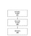
图1是示出了根据本发明的一个示例性实施例的用于设计系统的方法的流程图。FIG. 1 is a flowchart illustrating a method for designing a system according to an exemplary embodiment of the present invention.
图2是示出了根据本发明的一个示例性实施例的用于执行综合的方法的流程图。FIG. 2 is a flowchart illustrating a method for performing synthesis according to an exemplary embodiment of the present invention.
图3示出了根据本发明的一个示例性实施例的用于执行复位分析和去除的方法的流程图。FIG. 3 shows a flowchart of a method for performing reset analysis and removal according to an exemplary embodiment of the present invention.
图4示出了根据本发明的一个实施例的系统的冗余部分的第一示例。Figure 4 shows a first example of a redundant part of a system according to an embodiment of the invention.
图5示出了根据本发明的一个实施例的系统的冗余部分的第二示例。Figure 5 shows a second example of a redundant part of a system according to an embodiment of the invention.
图6示出了根据本发明的一个示例性实施例的用于执行同步复位标识的方法。FIG. 6 shows a method for performing synchronous reset identification according to an exemplary embodiment of the present invention.
图7示出了根据本发明的一个实施例的执行复位分析和去除的示例。Figure 7 shows an example of performing reset analysis and removal according to one embodiment of the present invention.
图8示出了根据本发明的一个实施例的实现了系统设计器的计算机系统的框图。FIG. 8 shows a block diagram of a computer system implementing a system designer according to one embodiment of the present invention.
图9是根据本发明的一个示例性实施例的系统设计器的框图,Figure 9 is a block diagram of a system designer according to an exemplary embodiment of the present invention,
图10是根据本发明的一个实施例的复位分析和去除单元的框图。Figure 10 is a block diagram of a reset analysis and removal unit according to one embodiment of the present invention.
图11示出了根据本发明的一个实施例的示例性目标装置。Figure 11 illustrates an exemplary target device according to one embodiment of the present invention.
发明内容Contents of the invention
根据本发明的一个实施例,在综合期间执行分析,该分析标识系统的在特定复位状态(condition)下变得冗余的部分,并且标识可以去除的复位。在去除复位之后,可以执行在综合中的优化,并且可以执行系统的布局和布线。根据本发明的一个方面,该分析包括标识系统中的复位信号。标识具有共同复位信号的寄存器集合。针对寄存器集合中的每个寄存器,应用复位状态,并且标识系统的冗余部分以及对该冗余部分指派成本值。针对寄存器集合中的尚未标记为去除的每个寄存器,按从最高到最低的成本顺序,应用复位状态,并且诸如复位信号连接之类的冗余的电路被标记用于去除。在已经按成本顺序分析了所有寄存器之后,在电路中的已被标记用于去除的寄存器被去除复位。According to one embodiment of the invention, an analysis is performed during synthesis that identifies parts of the system that become redundant under certain reset conditions and identifies resets that can be removed. After the reset is removed, optimization in synthesis can be performed, and placement and routing of the system can be performed. According to one aspect of the invention, the analysis includes identifying reset signals in the system. Identifies the set of registers that have a common reset signal. For each register in the set of registers, a reset state is applied, and a redundant portion of the system is identified and a cost value is assigned to the redundant portion. For each register in the register set that has not been marked for removal, in order of highest to lowest cost, the reset state is applied and redundant circuitry, such as reset signal connections, is marked for removal. After all registers have been analyzed in order of cost, the registers in the circuit that have been marked for removal are reset by removal.
具体实施方式Detailed ways
在下面的描述中,出于说明的目的,阐述了特定术语以提供对本发明的一些实施例的全面理解。对于本领域技术人员明显的是,可以无需说明书中的具体细节来实践本发明的一些实施例。在其它一些情形下,以框图的形式来显示熟知的电路、装置和程序以避免不必要地模糊本发明的一些实施例。In the following description, for purposes of explanation, specific terminology is set forth in order to provide a thorough understanding of some embodiments of the invention. It will be apparent to those skilled in the art that some embodiments of the invention may be practiced without the specific details in the specification. In other instances, well-known circuits, devices and procedures are shown in block diagram form in order to avoid unnecessarily obscuring some embodiments of the invention.
图1是说明了根据本发明的一个示例性实施例的用于在目标装置上设计系统的方法的流程图。目标装置可以是现场可编程门阵列(FPGA)、专用集成电路(ASIC)、结构化ASIC或其它装置。根据一个实施例,可以由在计算机系统上实现的计算机辅助设计(CAD)/电子设计自动化(EDA)工具来执行图1示出的过程。在101处,综合该系统。根据本发明的一个实施例,综合涉及生成待实现的系统的逻辑设计。FIG. 1 is a flowchart illustrating a method for designing a system on a target device according to an exemplary embodiment of the present invention. The target device may be a Field Programmable Gate Array (FPGA), Application Specific Integrated Circuit (ASIC), Structured ASIC, or other device. According to one embodiment, the process shown in FIG. 1 may be performed by a computer-aided design (CAD)/electronic design automation (EDA) tool implemented on a computer system. At 101, the system is integrated. According to one embodiment of the invention, synthesis involves generating a logical design of the system to be implemented.
图2是示出了根据本发明一个实施例的用于执行综合的方法的流程图。可以利用图2中所示的方法执行101。在201处,执行设计建立(elaboration)和提取。根据本发明的一个实施例,设计建立和提取包括根据系统的高级描述产生系统的逻辑表示。系统的高级描述可以是电路图、VHDL、Verilog或者其它设计定义的形式。逻辑表示可以包括那些包括如下表示:该表示包括系统所需的功能模块和寄存器(“部件”),该功能模块和寄存器诸如逻辑门和逻辑元件。在设计建立和提取期间,还可以执行初始优化。初始优化可以包括网表的清理(cleanout)以及恒定传播。在提取期间产生提取网表。FIG. 2 is a flowchart illustrating a method for performing synthesis according to one embodiment of the present invention. 101 can be executed by using the method shown in FIG. 2 . At 201, design elaboration and extraction is performed. According to one embodiment of the invention, design building and extraction includes generating a logical representation of the system from a high-level description of the system. A high-level description of the system can be in the form of a schematic, VHDL, Verilog, or other design definition. Logical representations may include those representations that include functional blocks and registers ("components") required by the system, such as logic gates and logic elements. During design setup and extraction, initial optimization can also be performed. Initial optimization may include cleanout of the netlist and constant propagation. An extraction netlist is generated during extraction.
在202处,根据提取网表来标识分区。根据本发明的一个实施例,分析寄存器复位以标识系统的在特定复位状态下变得冗余的部分。该分析涉及针对每个寄存器复位计算冗余效果的成本。基于计算的成本来去除与支持系统的这些冗余部分的寄存器复位相关联的电路。At 202, partitions are identified from the extracted netlist. According to one embodiment of the present invention, register resets are analyzed to identify parts of the system that become redundant in a particular reset state. The analysis involves calculating the cost of redundancy effects for each register reset. The circuitry associated with supporting register resets of these redundant parts of the system is removed based on computational cost.
在203处,对已修改的系统设计应用优化。复位分析和去除过程可以使得系统中的信号损失扇出或者在同步复位情形下设置为常数。该优化可以包括寄存器重定时、精细状态机重综合以及其它一些优化过程。优化可以包括RTL综合以及门级综合,在寄存器传输级(RTL)综合中大型/路线(course)模块被优化,而在门级综合中简易模块被优化。At 203, optimization is applied to the modified system design. The reset analysis and removal process can make signal loss in the system fan out or be set constant in case of synchronous reset. This optimization can include register retiming, fine state machine resynthesis, and other optimization procedures. Optimization can include RTL synthesis where large/course blocks are optimized and gate level synthesis where simple blocks are optimized.
在204处,对优化的逻辑设计执行映射(技术映射)。根据本发明的一个实施例,映射包括确定如何使用目标装置上可用的资源来实现优化逻辑表示中的逻辑门和逻辑元件。可用的资源可以包括LUT和其它一些资源。根据本发明的一个实施例,根据映射产生网表。该网表可以是根据HDL产生的优化的技术映射的网表。At 204, a mapping (technology mapping) is performed on the optimized logic design. According to one embodiment of the invention, mapping includes determining how to implement the logic gates and logic elements in the optimized logic representation using resources available on the target device. Available resources may include LUTs and other resources. According to one embodiment of the present invention, a netlist is generated from the mapping. The netlist may be an optimized technology-mapped netlist generated from HDL.
返回参考图1,在102处,在映射的逻辑系统设计中布局部件。对优化的技术映射网表进行布局以产生针对功能块中的每个功能块的布局。根据本发明的一个实施例,布局包括在目标装置上通过如下方式拟合系统:确定逻辑设计上的哪些资源待用于特定逻辑元件,以及其它一些功能块被确定实现在综合期间确定的系统。布局可以包括集群,其涉及将逻辑元件一起分组以形成在目标装置上出现的逻辑簇(cluster)。根据本发明的一个实施例,在布局的早先阶段执行集群,并且在布局预备阶段期间紧接综合之后产生集群。Referring back to FIG. 1 , at 102 components are placed in the mapped logical system design. The optimized technology-mapped netlist is placed to produce a placement for each of the functional blocks. According to one embodiment of the invention, layout includes fitting the system on the target device by determining which resources on the logic design are to be used for specific logic elements, and some other functional blocks are determined to implement the system determined during synthesis. Layout may include clustering, which involves grouping logical elements together to form logical clusters that appear on a target device. According to one embodiment of the present invention, clustering is performed in an early stage of placement, and the clustering is generated during the placement preparation stage immediately after synthesis.
在103处,对布局的设计进行布线。在布线期间,分配目标装置上的布线资源以在逻辑门、逻辑元件以及目标装置上的其它一些部件之间提供互连。也可以对布局的逻辑设计执行可布线性优化。根据本发明的一个实施例,可布线性优化的目标在于减少在布局的逻辑设计中用于连接部件的布线的量。可布线性优化可以包括执行扇出划分、逻辑复制、逻辑重布线或其它一些过程。应当理解,可以对布局的逻辑设计执行一个或者多个过程。At 103, the layout's design is routed. During routing, routing resources on the target device are allocated to provide interconnections between logic gates, logic elements, and other components on the target device. Routability optimization can also be performed on the placed logic design. According to one embodiment of the present invention, the objective of routability optimization is to reduce the amount of wiring used to connect components in a placed logic design. Routability optimization may include performing fan-out partitioning, logic duplication, logic rewiring, or some other process. It should be understood that one or more processes may be performed on the logical design of the layout.
在104处,执行汇编过程。汇编过程涉及产生包括了由101-103处描述的编译过程确定的信息的数据文件。该数据文件可以是可以用于对目标装置编程的位流。根据本发明的一个实施例,图1中示出的过程可以由在第一计算机系统上运行的EDA工具来执行。所产生的数据文件可以被发送至第二计算机系统以允许系统设计被进一步处理。备选地,该数据文件可以被发送至第二计算机系统,该第二计算机系统可以用于根据系统设计对目标装置编程。应当理解,也可以以其它形式输出系统设计,诸如在显示装置或者其它介质上输出系统设计。At 104, an assembly process is performed. The compilation process involves generating a data file that includes information determined by the compilation process described at 101-103. The data file can be a bit stream that can be used to program the target device. According to one embodiment of the present invention, the process shown in FIG. 1 may be performed by an EDA tool running on the first computer system. The resulting data file can be sent to a second computer system to allow the system design to be further processed. Alternatively, the data file can be sent to a second computer system which can be used to program the target device according to the system design. It should be understood that the system design may also be output in other forms, such as outputting the system design on a display device or other medium.
在105处,使用数据文件对目标装置编程。通过使用该数据文件对目标装置编程,将目标装置上的部件物理地转换以实现该系统。At 105, the target device is programmed using the data file. By programming the target device using the data file, the components on the target device are physically transformed to implement the system.
图3示出了根据本发明的一个实施例用于执行复位分析和去除的方法。图3中所示的方法可以在图2中202处实现。在301处,标识具有共用复位信号x的寄存器集合R(x)。根据本发明的一个实施例,寄存器集合具有数目被预定的最小数目的寄存器。在一个实施例中,该最小数目在十万的量级。Figure 3 illustrates a method for performing reset analysis and removal according to one embodiment of the present invention. The method shown in FIG. 3 can be implemented at 202 in FIG. 2 . At 301, a set of registers R(x) having a common reset signal x is identified. According to one embodiment of the invention, the set of registers has a predetermined minimum number of registers. In one embodiment, the minimum number is on the order of hundreds of thousands.
对寄存器集合R(x)中的每个寄存器执行过程302-305。Processes 302-305 are performed for each register in register set R(x).
在302处,复位状态被应用至寄存器集合R(x)中的之前尚未考虑的当前寄存器y。根据本发明的一个实施例,复位状态可以是使得寄存器输出0的复位信号。备选地,复位状态可以是使得寄存器输出1的预置信号。At 302, a reset state is applied to a current register y in register set R(x) that has not been considered before. According to an embodiment of the present invention, the reset state may be a reset signal that causes the register to output 0. Alternatively, the reset state may be a preset signal causing the register to
在303处,标识系统的冗余部分。根据本发明的一个实施例,系统的冗余部分是如下部分:在302处应用的复位状态下变得冗余的任何部分。At 303, redundant portions of the system are identified. According to one embodiment of the invention, a redundant part of the system is any part that becomes redundant in the reset state applied at 302 .
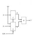
图4示出了根据本发明的一个实施例的系统的冗余部分的第一示例。图4示出了系统的具有两个寄存器(寄存器X和Y)以及逻辑门Z的一部分。寄存器X接收输入信号A,而寄存器Y接收输入信号B。寄存器X和寄存器Y由相同的时钟信号CLK钟控,并且共享共用复位信号。当触发复位时,寄存器X和寄存器Y这两者均输出0。由于逻辑门Z是AND门,因此当寄存器X和寄存器Y的输出中的至少一个输出为0时,逻辑门Z的输出是0。如果复位信号仅连接到寄存器X和寄存器Y之一,则逻辑门Z的输出应当相同。因此,在该示例中,当复位状态应用至寄存器X时,系统的冗余部分将包括寄存器Y。Figure 4 shows a first example of a redundant part of a system according to an embodiment of the invention. Figure 4 shows a part of the system with two registers (registers X and Y) and a logic gate Z. Register X receives input signal A and register Y receives input signal B. Register X and Register Y are clocked by the same clock signal CLK and share a common reset signal. Both register X and register Y output 0 when reset is triggered. Since logic gate Z is an AND gate, the output of logic gate Z is 0 when at least one of the outputs of register X and register Y is 0. If the reset signal is connected to only one of register X and register Y, then the output of logic gate Z should be the same. Thus, in this example, when a reset condition is applied to register X, the redundant portion of the system will include register Y.
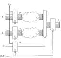
图5示出了根据本发明的一个实施例的系统的冗余部分的第二示例。图5示出了系统的、具有第一寄存器组P、第二寄存器组Q、控制寄存器R以及输出寄存器组Z的一部分。寄存器P接收输入信号A,而寄存器Q接收输入B。寄存器P、寄存器Q、寄存器R和寄存器Z由相同的时钟信号CLK钟控。寄存器P、寄存器Q和寄存器R共享共用复位信号。多路复用器M选择源自寄存器P或寄存器Q的输入。在复位状态下,控制寄存器R输出0,这使得无论寄存器Q的状态或者输出是什么,多路复用器M都选择源自寄存器P的输入。因此,在该示例中,当复位状态应用至寄存器R时,系统的冗余部分将包括寄存器Q。Figure 5 shows a second example of a redundant part of a system according to an embodiment of the invention. FIG. 5 shows a part of the system with a first register set P, a second register set Q, a control register R and an output register set Z. FIG. Register P receives input signal A, while register Q receives input B. Register P, Register Q, Register R and Register Z are clocked by the same clock signal CLK. Register P, Register Q, and Register R share a common reset signal. Multiplexer M selects the input from register P or register Q. In the reset state, the control register R outputs 0, which causes the multiplexer M to select the input from register P regardless of the state or output of register Q. Thus, in this example, when a reset condition is applied to register R, the redundant part of the system will include register Q.
返回参考图3,在304处,基于系统的所标识的冗余部分来计算当前寄存器y的成本。根据本发明的一个实施例,成本可以基于系统的变得冗余的分数(fraction)、变得冗余的逻辑门、寄存器的数目和/或接线的数目或长度、变得冗余的电路的深度或者其它一些度量。Referring back to FIG. 3 , at 304 , a cost for the current register y is calculated based on the identified redundant portion of the system. According to one embodiment of the invention, the cost may be based on the fraction of the system becoming redundant, the number of logic gates, the number of registers and/or the number or length of wiring, the number of circuits becoming redundant, Depth or some other measure.
在305处,确定是否已经对寄存器集合R(x)中的最后的寄存器(所有寄存器)计算了成本。如果尚未对寄存器集合中的最后寄存器计算成本,则控制返回至302处以对寄存器集合R(x)中的下一个寄存器执行过程302-304。如果已经对寄存器集合中的最后的寄存器计算成本,则控制进至306处。At 305, it is determined whether a cost has been calculated for the last register (all registers) in the set of registers R(x). If the cost has not been calculated for the last register in the set of registers, control returns to 302 to perform processes 302-304 on the next register in the set of registers R(x). Control proceeds to 306 if the cost has been calculated for the last register in the set of registers.
对寄存器集合R(x)中的、尚未被标记用于去除的每个寄存器执行过程306-309。Processes 306-309 are performed for each register in register set R(x) that has not been marked for removal.
在306处,复位状态应用至寄存器集合R(x)中的、之前尚未按成本顺序被标记用于去除的当前寄存器y。At 306, a reset state is applied to the current register y in the register set R(x) that has not been previously marked for removal in cost order.
在307处,系统的、通过应用复位状态得到的冗余部分被标记用于去除。At 307, redundant portions of the system obtained by applying the reset state are marked for removal.
在308处,确定寄存器集合R(x)中的、之前尚未被标记用于去除的最后寄存器y是否已被应用了复位状态。如果寄存器集合中的、之前尚未被标记用于去除的最后寄存器y尚未被应用复位状态,则控制返回至306以对寄存器集合中的下一个寄存器执行过程306-307。如果寄存器集合中的、之前尚未被标记用于去除的最后寄存器y已被应用复位状态,则控制进至309。At 308, it is determined whether the last register y in the set of registers R(x) that has not been previously marked for removal has had the reset state applied. If the last register y in the set of registers that was not previously marked for removal has not had the reset state applied, control returns to 306 to perform processes 306-307 on the next register in the set of registers. If the last register y in the register set that has not been previously marked for removal has had the reset state applied, then control passes to 309 .
在309处,去除被标记用于去除的每个寄存器处的复位。At 309, the reset at each register marked for removal is removed.
应当理解,过程301-309可以被重复,并且被应用至系统中其它寄存器集合以标识其它一些待去除的复位。还应当理解,图3中描述的方法可以用于执行复位分析以及异步复位或同步复位的去除。图3中描述的方法中的过程301-309应当分别应用至每组复位(异步地或同步地)。根据本发明的一个实施例,过程301-309在被应用至同步复位之前被应用至异步复位。It should be understood that the process 301-309 can be repeated and applied to other sets of registers in the system to identify other resets to be removed. It should also be understood that the method described in FIG. 3 can be used to perform reset analysis and removal of asynchronous or synchronous resets. Procedures 301-309 in the method described in FIG. 3 should be applied to each set of resets (either asynchronously or synchronously) respectively. According to one embodiment of the invention, processes 301-309 are applied to asynchronous resets before being applied to synchronous resets.
根据本发明的一个实施例,当去除在被标记用于去除的寄存器处的同步复位时,如果在寄存器处存在同步复位,则去除复位。然而,如果复位信号耦合至数据输入,则连接可以通过单个扇出节点从所述寄存器回溯至同步复位信号,其中复位信号被设置为相反值。According to one embodiment of the invention, when removing a synchronous reset at a register marked for removal, the reset is removed if there is a synchronous reset at the register. However, if a reset signal is coupled to a data input, the connection can be traced back from the register to a synchronous reset signal via a single fanout node, where the reset signal is set to the opposite value.
图6示出了根据本发明一个实施例的用于执行同步复位标识的方法。可以在使用图3中描述的方法之前执行图6中描述的方法,以对同步复位执行复位分析和去除。在601处,标识信号i,该信号i具有大于第一阈值数目的扇出数目。FIG. 6 shows a method for performing synchronous reset identification according to one embodiment of the present invention. The method described in FIG. 6 may be performed prior to using the method described in FIG. 3 to perform reset analysis and removal for synchronous resets. At 601, a signal i is identified having a fanout number greater than a first threshold number.
在602处,数值1被指派至该信号。At 602, a value of 1 is assigned to the signal.
在603处,在将数值1指派至该信号的情形下,在评估逻辑状态之后,标识具有恒定输入的寄存器的第一数目。At 603, a first number of registers with constant inputs are identified after evaluating the logic state in case the
在604处,数值0被指派至该信号。At 604, a value of 0 is assigned to the signal.
在605处,在将数值0指派至该信号的情形下,在评估逻辑状态之后,标识具有恒定输入的寄存器的第二数目。At 605, a second number of registers with constant inputs are identified after evaluating the logic state in case the value 0 is assigned to the signal.
在606处,确定寄存器的第一数目或者寄存器的第二数目中的较大者是否大于第二阈值数目。如果寄存器的第一数目或寄存器的第二数目中的较大者大于所述第二阈值数目,则控制进至607。如果寄存器的第一数目或寄存器的第二数目中的较大者不大于第二阈值数目,则控制进至608。At 606, it is determined whether the greater of the first number of registers or the second number of registers is greater than a second threshold number. If the greater of the first number of registers or the second number of registers is greater than the second threshold number, then control proceeds to 607 . If the greater of the first number of registers or the second number of registers is not greater than the second threshold number, control proceeds to 608 .
在607处,该信号被指定为复位信号。At 607, the signal is designated as a reset signal.
在608处,该信号不被指定为复位信号。At 608, the signal is not designated as a reset signal.
应当理解,可以重复过程601-608,并且将过程601-608应用至其它一些信号以确定信号是否为复位信号。It should be understood that the processes 601-608 may be repeated and applied to some other signals to determine whether the signal is a reset signal.
参考上述过程,应当理解,可以使用第一预定阈值和第二预定阈值。第一预定阈值可以用于首先标识具有高扇出的信号。第二预定阈值可以用于标识如下寄存器,该寄存器在标识信号是否为同步复位之前变得恒定。根据本发明的一个方面,第一预定阈值可以大于第二预定阈值。With reference to the process described above, it should be understood that a first predetermined threshold and a second predetermined threshold may be used. The first predetermined threshold may be used to first identify signals with high fanout. The second predetermined threshold may be used to identify a register that becomes constant before identifying whether the signal is a synchronous reset. According to an aspect of the present invention, the first predetermined threshold may be greater than the second predetermined threshold.
根据本发明的一个实施例,标识可以用作复位或者预置信号的信号。如果使得寄存器变为0,则信号是“复位”。如果使得寄存器变为1,则信号是“预置”。对于异步复位/预置而言,可以通过检查寄存器上与信号耦合的端口是复位端口还是预置端口来标识信号是复位还是预置。对于同步复位/预置而言,可能需要分析以标识信号是复位还是预置。分析可以涉及首先标识具有高扇出且可以潜在地设置寄存器为1或者0的信号。接着,确定当信号设置为1或者0时会发生什么。如果大量(大于阈值数目)寄存器变为0,则标识为复位。但是,如果大量寄存器变为1,则标识为预置。According to one embodiment of the invention, a signal that can be used as a reset or preset signal is identified. If the register becomes 0, the signal is "reset". If the register becomes 1, the signal is "preset". For asynchronous reset/preset, it is possible to identify whether the signal is reset or preset by checking whether the port coupled to the signal on the register is a reset port or a preset port. For synchronous reset/preset, analysis may be required to identify whether the signal is a reset or preset. Analysis may involve first identifying signals that have high fanout and can potentially set registers to 1 or 0. Next, determine what happens when the signal is set to 1 or 0. A reset is flagged if a large number (greater than a threshold number) of registers go to 0. However, if a large number of registers become 1, it is identified as preset.
图1-图3和图6是示出本发明一些实施例的流程图。示出的一些技术可以顺序地执行、并行地执行或者按除所述顺序之外的顺序执行,并且可以重复该过程。应当理解,并非要求执行所有描述的技术,可以添加其它一些技术,并且示出的一些技术可以替换为其它一些技术。1-3 and 6 are flowcharts illustrating some embodiments of the invention. Some of the techniques shown may be performed sequentially, in parallel, or in an order other than that described, and the process may be repeated. It should be understood that not all described techniques are required to be performed, that other techniques may be added, and that some of the techniques shown may be substituted for other techniques.
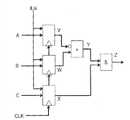
图7示出了根据本发明一个实施例的执行复位分析和去除的示例。图7示出了系统的、具有寄存器V、寄存器W和寄存器X的一部分。寄存器V接收输入信号A。寄存器W接收输入信号B。寄存器X接收输入信号C。寄存器V、寄存器W和寄存器X由CLK钟控,并且共享复位信号。逻辑门Y是OR门,而逻辑门Z是AND门。Figure 7 shows an example of performing reset analysis and removal according to one embodiment of the present invention. Figure 7 shows a part of the system with register V, register W and register X. Register V receives input signal A. Register W receives input signal B. Register X receives input signal C. Register V, Register W, and Register X are clocked by CLK and share a reset signal. Logic gate Y is an OR gate while logic gate Z is an AND gate.
参见图3,在301处,寄存器V、寄存器W和寄存器X标识为具有共用复位。Referring to FIG. 3, at 301, register V, register W, and register X are identified as having a common reset.
在302和303处,当复位状态应用至寄存器V时,寄存器V的输出变成0。V的输出在被输入进逻辑门Y之前经过反相器。在对逻辑门Y输入为1的输入的情形下,不论来自寄存器W的输入是多少,逻辑门Y总是输出1。因此,来自寄存器W的输入变得冗余。因为逻辑门Z是AND门,因此逻辑门Z的、来自寄存器X的输入仍然是相关的。At 302 and 303, when a reset condition is applied to register V, the output of register V becomes 0. The output of V passes through an inverter before being input into logic gate Y. In case of an input of 1 to logic gate Y, logic gate Y always outputs 1 regardless of the input from register W. Therefore, the input from register W becomes redundant. Since logic gate Z is an AND gate, the input of logic gate Z from register X is still relevant.
在304处,对于冗余部分的成本而言,寄存器W是1个寄存器。应当理解,可以使用其它一些度量来估计冗余部分的成本。At 304, the register W is 1 register for the cost of the redundant portion. It should be understood that other metrics may be used to estimate the cost of the redundant portion.
在305处,寄存器V不是寄存器集合中被分析成本的最后寄存器。控制返回至302以评估寄存器W。At 305, register V is not the last register in the set of registers whose cost is analyzed. Control returns to 302 to evaluate register W.
在302和303处,当复位状态应用至寄存器W时,寄存器W的输出变成0。W的输出是逻辑门Y的输入。因为逻辑门Y是OR门,逻辑门Y的其它输入仍然是相关的。因此,当复位状态应用至寄存器W时,系统没有冗余部分。At 302 and 303, when a reset condition is applied to register W, the output of register W becomes 0. The output of W is the input of logic gate Y. Since logic gate Y is an OR gate, the other inputs of logic gate Y are still relevant. Therefore, when the reset state is applied to register W, there is no redundant part of the system.
在304处,冗余部分的成本是0。At 304, the cost of the redundant portion is zero.
在305处,寄存器W不是寄存器集合中的被分析成本的最后寄存器。控制返回至302以评估寄存器X。At 305, register W is not the last register in the set of registers whose cost is analyzed. Control returns to 302 to evaluate register X.
在302和303处,当复位状态应用至寄存器X时,寄存器X的输出变成0。因为逻辑门Z是AND门,其中来自寄存器X的输入为0,因此不论来自逻辑门Y的输入是什么,逻辑门Z总是输出0。因此,来自逻辑门Y的输入变得冗余,并且逻辑门Y和寄存器V和寄存器W是冗余的。At 302 and 303, when a reset condition is applied to register X, the output of register X becomes 0. Because logic gate Z is an AND gate where the input from register X is 0, logic gate Z will always output 0 no matter what the input from logic gate Y is. Therefore, the input from logic gate Y becomes redundant, and logic gate Y and register V and register W are redundant.
在304处,冗余部分(逻辑门Y和寄存器V和寄存器W)的成本是1个逻辑门和2个寄存器。应当理解,可以使用其它度量来估计冗余部分的成本。At 304, the cost of the redundant part (logic gate Y and register V and register W) is 1 logic gate and 2 registers. It should be understood that other metrics may be used to estimate the cost of redundancy.
在305处,因为已分析了寄存器V、寄存器W和寄存器X的成本,控制进至306。At 305, because the cost of register V, register W, and register X has been analyzed, control proceeds to 306.
在306处,最高成本顺序的寄存器确定为寄存器X。因为寄存器X并未标记以用于去除,复位状态应用至寄存器X。At 306, the highest cost ordered register is determined to be register X. Because register X is not marked for removal, the reset state applies to register X.
在307处,标记冗余部分(逻辑门Y和寄存器V和W)用于去除。At 307, redundant portions (logic gate Y and registers V and W) are marked for removal.
在308处,因为寄存器X是寄存器集合中尚未被标记但已经被分析的最后寄存器,控制进至309。At 308, control passes to 309 because register X is the last register in the set of registers that has not been marked but has been analyzed.
在309处,去除每个被标记用于去除的寄存器处的复位。At 309, the reset at each register marked for removal is removed.
图7中示出的示例可以用于异步复位或者用于同步复位。应当理解,当去除用于同步复位的复位时,如果在寄存器(SCLR)处出现同步复位,则可以去除复位。备选地,如果在寄存器处未出现同步复位,可以通过单个扇出节点从寄存器向同步复位信号执行回溯(tracebackward)。继而可以通过将复位信号设置为相反值而去除该复位信号。The example shown in Figure 7 can be used for an asynchronous reset or for a synchronous reset. It should be understood that when removing a reset for a synchronous reset, the reset may be removed if a synchronous reset occurs at the register (SCLR). Alternatively, if no synchronous reset occurs at the register, a traceback can be performed from the register to the synchronous reset signal through a single fanout node. The reset signal can then be removed by setting the reset signal to the opposite value.
图8示出了根据本发明一个实施例的实现系统设计器的计算机系统的框图。如图所示,计算机系统800包括处理器801。处理器801耦合至CPU总线810,CPU总线810在处理器801和计算机系统800中其它一些部件之间传输数据信号。FIG. 8 shows a block diagram of a computer system implementing a system designer according to one embodiment of the present invention. As shown,
计算机系统800包括存储器813。存储器813可以是动态随机访问存储器装置、静态随机访问存储器装置、和/或其它存储器装置。存储器813可以存储由数据信号表示的、可以由处理器801运行的指令和代码。桥接存储器控制器811耦合至CPU总线810和存储器813。桥接存储器控制器811在处理器801、存储器813和计算机系统800中其它一些部件之间引导数据信号,并且桥接存储器控制器811在CPU总线810、存储器813和第一IO总线820之间桥接数据信号。
第一IO总线820可以是单个总线或者多个总线的组合。第一IO总线820在计算机系统800中的一些部件之间提供通信链路。网络控制器821耦合至第一IO总线820。网络控制器821可以将计算机系统800链接至计算机网络(未示出),并且支持在机器之间的通信。显示装置控制器822耦合至第一IO总线820。显示装置控制器822允许显示装置(未示出)耦合至计算机系统800,并且用作显示装置和计算机系统800之间的接口。The
第二IO总线830可以是单个总线或者多个总线的组合。第二IO总线830在计算机系统800中的一些部件之间提供通信链路。数据存储装置831耦合至第二IO总线830。数据存储装置831可以是硬盘驱动器、软盘驱动器、CD-ROM装置、闪存装置或其它大容量存储装置。输入接口832耦合至第二IO总线830。输入接口832允许输入装置耦合至计算机系统800,并且将数据信号从输入装置传输至计算机系统100。总线桥823将第一IO总线820耦合至第二IO总线830。总线桥823操作成在第一IO总线820和第二IO总线830之间缓冲和桥接数据信号。应当理解,也可以使用具有不同架构的计算机系统以实现计算机系统800。The
系统设计器840可以驻留在存储器813中,并且由处理器801执行。系统设计器840可以操作成综合系统、在目标装置上布局系统、布线系统、汇编系统和对目标装置编程以实现系统。在综合期间,可以由系统设计器840执行分析以标识系统的在特定复位状态下变得冗余的部分并且标识可以去除的复位。在去除所标识的复位之后,可以执行对综合的优化。
图9示出了根据本发明一个示例性实施例的系统设计器900。系统设计器900可以用于实现图8中所示的系统设计器840,并且可以执行图1-图3和图6中描述的过程。系统设计器900可以是用于在目标装置上设计系统的CAD工具。目标装置可以是例如ASIC、结构化ASIC、FPGA、可编程逻辑器件(PLD)、印刷电路板(PCB)或其它一些电路。图9示出了实现系统设计器900的实施例的模块。根据一个实施例,系统设计可以由运行由图9中所示的模块表示的指令的序列的计算机系统执行,诸如例如图8中示出的计算机系统。指令序列的执行使得计算机系统支持如下文描述的系统设计。在一些备选的实施例中,硬接线电路可以用于替代软件指令或者与软件指令相组合以实现本发明。因此,本发明不限于硬件电路和软件的任何特定组合。系统设计器900包括系统设计器管理器910。系统设计器管理器910连接至系统设计器900的一些部件,并且在上述部件之间传输数据。系统设计管理器910也可以执行关于设计信息的设计建立,该设计信息被输入进系统设计器900。设计建立可以包括检阅设计信息以确保信息的语法是正确的。FIG. 9 shows a
模块920表示综合单元。根据本发明的一个实施例,综合单元920执行设计建立和提取,其包括根据系统的高层次描述产生的系统的逻辑表示。系统的高层次描述可以是电路图、VHDL、Verilog或其它一些设计定义的形式。逻辑表示可以包括如下表示,该表示包括系统所需的诸如逻辑门和逻辑元件之类的功能模块和寄存器(“部件”)。综合单元920包括复位分析和去除单元921,综合单元920分析寄存器复位以标识系统的、在特定复位状态下变得冗余的部分。分析涉及针对每个寄存器复位计算冗余效果的成本。基于所计算的成本来去除与支持系统的冗余部分的寄存器复位相关联的电路。在去除与支持系统的冗余部分的寄存器复位相关联的电路之后,将优化应用至修改的系统设计。优化可以包括寄存器重定时、精细状态机重综合和其它一些优化过程。优化可以包括优化大型/路线模块的RTL综合以及优化简易模块的门级综合。综合单元920也对优化的逻辑设计执行映射(技术映射)。根据本发明的一个实施例,映射包括确定如何使用目标装置上可用资源在优化的逻辑表示中实现逻辑门和逻辑元件。可用资源可以包括LUT和其它一些资源。根据本发明的一个实施例,根据映射产生网表。该网表可以是根据HDL产生的优化的技术映射网表。
模块930表示布局单元。布局单元930通过确定目标装置上的哪个部件或区域待用于特定功能模块和寄存器来将系统布局到目标装置上。根据系统设计器900的一个实施例,布局单元930首先确定如何以簇的形式实现优化逻辑设计的一些部分。簇可以表示在逻辑设计上的部件的子集。例如,簇可以由一起分组的许多标准单元表示。在该实施例中,以簇的形式实现优化的逻辑设计的一些部分之后,可以通过将簇指派给目标装置上的特定位置而布局簇。布局单元930可以利用成本函数以便于确定目标装置上资源的良好指派。
模块940表示布线单元。布线单元940确定在目标装置上的布线资源,该布线资源用于提供在实现逻辑设计的功能模块和寄存器的组件之间的互连。
模块950表示汇编单元。汇编单元950产生数据文件,数据文件包括由系统设计器900执行的编译过程所确定的信息。数据文件可以是用于对目标装置编程的位流。根据本发明的一个实施例,所产生的数据文件可以传输至另一计算机系统以允许进一步处理系统设计。备选地,数据文件可以传输至另一计算机系统,该另一计算机系统可以用于根据系统设计对目标装置编程。通过使用数据文件对目标装置编程,目标装置上的部件发生物理转变以实现系统。应当理解,也可以以其它形式输出系统设计,诸如在显示装置或者其它介质上输出系统设计。
图10是根据本发明一个实施例的复位分析和去除单元1000的框图。复位分析和去除单元1000可以用于实现图9中所示的复位分析和去除单元921。复位分析和去除单元1000包括复位分析和去除管理器1010。复位分析和去除管理器1010耦合至复位分析和去除单元1000中的一些部件并在上述部件之间传输信息。FIG. 10 is a block diagram of a reset analysis and
复位分析和去除单元1000包括复位标识单元1020。复位标识单元1020操作成标识同步复位。根据本发明的一个实施例,复位标识单元1020可以执行图6中示出的过程以根据系统中的信号标识同步复位。The reset analysis and
复位分析和去除单元1000包括冗余部分标识单元1030。根据本发明的一个实施例,冗余部分标识单元1030通过标识具有共用同步复位x的寄存器集合R(x)、每次向寄存器集合R(x)中的每个寄存器y应用复位状态并且分析系统中的逻辑状态来标识系统中冗余部分,从而标识系统中的、当应用复位状态时不影响系统中其它一些逻辑的部分。The reset analysis and
复位分析和去除单元1000包括成本计算单元1040。成本计算单元1040基于所标识的系统的冗余部分来计算每个寄存器y的成本。根据本发明的一个实施例,成本可以基于系统的变得冗余的分数、变得冗余的逻辑门的数目和/或引线的数目或长度、变得冗余的电路的深度或者其它度量。The reset analysis and
复位分析和去除单元1000包括复位去除单元1050。复位去除单元1050向寄存器集合R(x)中的、之前尚未按成本顺序被标记用于去除的每个寄存器y应用复位状态。复位去除单元1050标记系统的通过如下方式得到的冗余部分:应用复位状态用于去除,直至存器R(x)中的之前尚未被标记用于去除的所有寄存器已被应用复位状态。随后去除在被标记用于去除的每个寄存器处的复位。当去除在已被标记用于去除的寄存器处的同步复位时,如果于寄存器处存在同步复位,则去除复位。然而,如果复位信号耦合至数据输入,则连接可以通过单个扇出节点从寄存器回溯至同步复位信号,在该同步复位信号处复位信号被设置为相反值。The reset analysis and
已经参考标识和去除冗余复位信号论述了本发明的一些实施例。应当理解,本发明的一些实施例也可以用于以相同方式标识和去除冗余预置信号。Some embodiments of the invention have been discussed with reference to identifying and removing redundant reset signals. It should be understood that some embodiments of the present invention can also be used to identify and remove redundant preset signals in the same manner.
应当理解,可以以计算机程序产品或者软件的形式提供本发明的一些实施例,其可以包括具有指令的计算机可读或者机器可读介质。计算机可读或者机器可读介质上的指令可以用于对计算机系统或者其它电子装置编程。机器可读介质可以包括但不限于软盘、光盘、CD-ROM和磁光盘或者适于存储电子指令的其它类型介质/机器可读介质。在此描述的技术并不限于任何特定的软件结构。它们可以应用到任何计算或者处理环境中。在此使用的术语“计算机可读介质”或者“机器可读介质”将包括能够存储或者编码由计算机执行并且使得计算机执行在此描述的任一方法的指令序列的任何介质。此外,在本领域中,涉及的软件以一种或者另一种形式采取动作或引起结果(例如程序、过程、处理、应用、模块、单元、逻辑等等)是常见的。这些表述仅仅是陈述处理系统对软件的执行使得处理器执行动作以产生结果的简要方式。It should be understood that some embodiments of the invention may be provided in the form of a computer program product or software, which may include a computer-readable or machine-readable medium having instructions. The instructions on the computer-readable or machine-readable medium may be used to program a computer system or other electronic device. Machine-readable media may include, but are not limited to, floppy disks, optical disks, CD-ROMs, and magneto-optical disks, or other types of media/machine-readable media suitable for storing electronic instructions. The techniques described here are not limited to any particular software architecture. They can be applied to any computing or processing environment. The term "computer-readable medium" or "machine-readable medium" as used herein shall include any medium capable of storing or encoding a sequence of instructions which are executed by a computer and which cause the computer to perform any of the methods described herein. Furthermore, it is common in the art to refer to software, in one form or another, taking an action or causing a result (eg program, procedure, process, application, module, unit, logic, etc.). These expressions are merely a shorthand way of stating that execution of the software by a processing system causes the processor to perform actions to produce results.
图11说明了根据本发明的一个实施例的可以用于实现目标装置的装置1100。装置1100是包括多个逻辑阵列块(LAB)的现场可编程门阵列(FPGA)。每个LAB可以由多个逻辑块、进位链、LAB控制信号、查找表(LUT)链和寄存器链连接线形成。逻辑块是提供用户逻辑功能的有效实现的小的逻辑单元。逻辑块包括一个或多个组合的单元和寄存器,其中每个组合的单元具有单个输出。根据本发明的一个实施例,所述逻辑块可以按照诸如Altera
装置1100包括存储块。例如,存储块可以例如是提供高达各种频率下的高达各种位宽的专用真实双端口、简单双端口或单端口存储器的双端口随机访问存储器(RAM)块。存储块可以遍布装置地在所选LAB之间分组为列,或者分别或成对地位于装置1100内。存储块的列示出为1121-1124。Apparatus 1100 includes a memory block. For example, the memory blocks may be, for example, dual-port random access memory (RAM) blocks providing dedicated real dual-port, simple dual-port or single-port memory up to various frequencies and up to various bit widths. Memory blocks may be grouped into columns between selected LABs throughout the device, or located within device 1100 individually or in pairs. The columns of storage blocks are shown as 1121-1124.
装置1100包括数字信号处理(DSP)块。DSP块可以用于实现具有加法或者减法特征的各种配置的乘法器。DSP块包括移位寄存器、乘法器、加法器和累加器。DSP块可以在遍布装置1100地分组为列并且示出为1131。Apparatus 1100 includes digital signal processing (DSP) blocks. The DSP blocks can be used to implement various configurations of multipliers with addition or subtraction features. DSP blocks include shift registers, multipliers, adders, and accumulators. DSP blocks may be grouped throughout device 1100 into columns and shown as 1131 .
装置1100包括多个输入/输出元件(IOE)1140。每个IOE对在装置1100上IO管脚(未示出)进行馈送。IOE 1140位于装置1100的边缘周围的LAB行和列的端部。每个IOE可以包括双向IO缓存器和多个用于寄存输入、输出和输出使能信号的寄存器。Apparatus 1100 includes a plurality of input/output elements (IOEs) 1140 . Each IOE feeds an IO pin (not shown) on device 1100 . IOEs 1140 are located at the ends of LAB rows and columns around the edge of device 1100. Each IOE may include a bidirectional IO buffer and multiple registers for registering input, output and output enable signals.
装置1100可以包括布线资源,诸如LAB局部互连线、行互连线(“H型引线”)和列互连线(“V型引线”)(未示出),以在目标装置上的部件之间路由信号布线。Device 1100 may include routing resources, such as LAB local interconnect lines, row interconnect lines ("H-leads"), and column interconnect lines ("V-leads") (not shown) to route components on the target device Routing signal wiring between.
在前述说明书中,已参照其特定示例性实施例描述了本发明的一些实施例。然而,明显的是,可以对其做出各种修改和改变而不脱离本发明所述实施例的宽广精神和范围。因此,所述说明书和附图应视作示例性的而不是限制性的。In the foregoing specification, some embodiments of the invention have been described with reference to specific exemplary embodiments thereof. It will, however, be evident that various modifications and changes may be made thereto without departing from the broad spirit and scope of the described embodiments of the invention. Accordingly, the specification and drawings are to be regarded as illustrative rather than restrictive.
Claims (28)
Translated fromChineseApplications Claiming Priority (3)
| Application Number | Priority Date | Filing Date | Title |
|---|---|---|---|
| US12/800,227 | 2010-05-11 | ||
| US12/800,227US8578306B2 (en) | 2010-05-11 | 2010-05-11 | Method and apparatus for performing asynchronous and synchronous reset removal during synthesis |
| PCT/US2011/035807WO2011143141A2 (en) | 2010-05-11 | 2011-05-09 | Method and apparatus for performing asynchronous and synchronous reset removal during synthesis |
Publications (2)
| Publication Number | Publication Date |
|---|---|
| CN102893282Atrue CN102893282A (en) | 2013-01-23 |
| CN102893282B CN102893282B (en) | 2015-11-25 |
Family
ID=44912853
Family Applications (1)
| Application Number | Title | Priority Date | Filing Date |
|---|---|---|---|
| CN201180023477.6AExpired - Fee RelatedCN102893282B (en) | 2010-05-11 | 2011-05-09 | For performing method and the equipment of asynchronous and synchronous reset removal in comprehensive period |
Country Status (5)
| Country | Link |
|---|---|
| US (1) | US8578306B2 (en) |
| EP (1) | EP2569723A4 (en) |
| JP (1) | JP5779237B2 (en) |
| CN (1) | CN102893282B (en) |
| WO (1) | WO2011143141A2 (en) |
Cited By (1)
| Publication number | Priority date | Publication date | Assignee | Title |
|---|---|---|---|---|
| CN106257467A (en)* | 2015-06-22 | 2016-12-28 | 阿尔特拉公司 | For the method and apparatus utilizing estimation when resetting for depositor in design and compilation flow process |
Families Citing this family (5)
| Publication number | Priority date | Publication date | Assignee | Title |
|---|---|---|---|---|
| US9424382B1 (en)* | 2013-11-20 | 2016-08-23 | Altera Corporation | Method and apparatus for providing fault tolerance through compilation diversity |
| US9053271B1 (en) | 2014-02-06 | 2015-06-09 | Freescale Semiconductor, Inc. | Integrated circuit reset system modification tool |
| US9685957B2 (en)* | 2014-04-09 | 2017-06-20 | Altera Corporation | System reset controller replacing individual asynchronous resets |
| US9171116B1 (en)* | 2014-09-16 | 2015-10-27 | Cadence Design Systems, Inc. | Method and system for reducing redundant logic in an integrated circuit |
| US9715564B2 (en) | 2015-10-28 | 2017-07-25 | International Business Machines Corporation | Scalable and automated identification of unobservability causality in logic optimization flows |
Citations (5)
| Publication number | Priority date | Publication date | Assignee | Title |
|---|---|---|---|---|
| US6526559B2 (en)* | 2001-04-13 | 2003-02-25 | Interface & Control Systems, Inc. | Method for creating circuit redundancy in programmable logic devices |
| US20070220453A1 (en)* | 2006-03-02 | 2007-09-20 | Hiroshi Tobita | Method for forming reset operation verifying circuit |
| US7343569B1 (en)* | 2003-07-15 | 2008-03-11 | Altera Corporation | Apparatus and method for reset distribution |
| US7594211B1 (en)* | 2006-11-17 | 2009-09-22 | Synopsys, Inc. | Methods and apparatuses for reset conditioning in integrated circuits |
| CN101551764A (en)* | 2009-02-27 | 2009-10-07 | 北京时代民芯科技有限公司 | An anti-SEE system and method based on synchronizing redundant threads and coding technique |
Family Cites Families (5)
| Publication number | Priority date | Publication date | Assignee | Title |
|---|---|---|---|---|
| US4816999A (en)* | 1987-05-20 | 1989-03-28 | International Business Machines Corporation | Method of detecting constants and removing redundant connections in a logic network |
| US5461574A (en)* | 1989-03-09 | 1995-10-24 | Fujitsu Limited | Method of expressing a logic circuit |
| JP2967761B2 (en)* | 1997-06-06 | 1999-10-25 | 日本電気株式会社 | Logic synthesis method and apparatus |
| US7622947B1 (en)* | 2003-12-18 | 2009-11-24 | Nvidia Corporation | Redundant circuit presents connections on specified I/O ports |
| JP5146369B2 (en)* | 2009-03-11 | 2013-02-20 | 富士通セミコンダクター株式会社 | Circuit design program, circuit design method, and circuit design apparatus |
- 2010
- 2010-05-11USUS12/800,227patent/US8578306B2/ennot_activeExpired - Fee Related
- 2011
- 2011-05-09JPJP2013510216Apatent/JP5779237B2/ennot_activeExpired - Fee Related
- 2011-05-09CNCN201180023477.6Apatent/CN102893282B/ennot_activeExpired - Fee Related
- 2011-05-09EPEP11781101.8Apatent/EP2569723A4/ennot_activeWithdrawn
- 2011-05-09WOPCT/US2011/035807patent/WO2011143141A2/enactiveApplication Filing
Patent Citations (5)
| Publication number | Priority date | Publication date | Assignee | Title |
|---|---|---|---|---|
| US6526559B2 (en)* | 2001-04-13 | 2003-02-25 | Interface & Control Systems, Inc. | Method for creating circuit redundancy in programmable logic devices |
| US7343569B1 (en)* | 2003-07-15 | 2008-03-11 | Altera Corporation | Apparatus and method for reset distribution |
| US20070220453A1 (en)* | 2006-03-02 | 2007-09-20 | Hiroshi Tobita | Method for forming reset operation verifying circuit |
| US7594211B1 (en)* | 2006-11-17 | 2009-09-22 | Synopsys, Inc. | Methods and apparatuses for reset conditioning in integrated circuits |
| CN101551764A (en)* | 2009-02-27 | 2009-10-07 | 北京时代民芯科技有限公司 | An anti-SEE system and method based on synchronizing redundant threads and coding technique |
Cited By (1)
| Publication number | Priority date | Publication date | Assignee | Title |
|---|---|---|---|---|
| CN106257467A (en)* | 2015-06-22 | 2016-12-28 | 阿尔特拉公司 | For the method and apparatus utilizing estimation when resetting for depositor in design and compilation flow process |
Also Published As
| Publication number | Publication date |
|---|---|
| EP2569723A4 (en) | 2017-10-11 |
| US20110283250A1 (en) | 2011-11-17 |
| JP5779237B2 (en) | 2015-09-16 |
| WO2011143141A3 (en) | 2012-02-16 |
| CN102893282B (en) | 2015-11-25 |
| EP2569723A2 (en) | 2013-03-20 |
| JP2013526738A (en) | 2013-06-24 |
| US8578306B2 (en) | 2013-11-05 |
| WO2011143141A2 (en) | 2011-11-17 |
Similar Documents
| Publication | Publication Date | Title |
|---|---|---|
| US11093672B2 (en) | Method and apparatus for performing fast incremental physical design optimization | |
| JP4923128B2 (en) | Circuit design and retiming method and apparatus | |
| US6009256A (en) | Simulation/emulation system and method | |
| US8732634B1 (en) | Method and apparatus for performing fast incremental resynthesis | |
| US8381142B1 (en) | Using a timing exception to postpone retiming | |
| US8918748B1 (en) | M/A for performing automatic latency optimization on system designs for implementation on programmable hardware | |
| US8468476B1 (en) | Method and apparatus for designing a system on multiple field programmable gate array device types | |
| CN102893282B (en) | For performing method and the equipment of asynchronous and synchronous reset removal in comprehensive period | |
| US8832618B1 (en) | Method and apparatus for automatic hierarchical design partitioning | |
| US9298872B2 (en) | Apportioning synthesis effort for better timing closure | |
| US9292638B1 (en) | Method and apparatus for performing timing closure analysis when performing register retiming | |
| EP3109780A1 (en) | Method and apparatus for utilizing estimations for register retiming in a design compilation flow | |
| US8504970B1 (en) | Method and apparatus for performing automated timing closure analysis for systems implemented on target devices | |
| US8793629B1 (en) | Method and apparatus for implementing carry chains on FPGA devices | |
| US9646126B1 (en) | Post-routing structural netlist optimization for circuit designs | |
| US8954906B1 (en) | Method and apparatus for performing parallel synthesis on a field programmable gate array | |
| US9230047B1 (en) | Method and apparatus for partitioning a synthesis netlist for compile time and quality of results improvement | |
| US9275184B1 (en) | Method and apparatus for performing timing closure analysis when performing register retiming | |
| CN113761820A (en) | Programmable integrated circuit bottom layer | |
| US10223488B2 (en) | Method and apparatus for improving system operation by replacing components for performing division during design compilation | |
| US7509597B1 (en) | Method and apparatus for performing post-placement functional decomposition on field programmable gate arrays using binary decision diagrams | |
| US11507723B2 (en) | Method and apparatus for performing incremental compilation using structural netlist comparison | |
| US8201114B1 (en) | Method and apparatus for performing look up table unpacking and repacking for resynthesis | |
| US8281271B1 (en) | Method and apparatus for performing lutmask based delay modeling | |
| US8661385B1 (en) | Method and apparatus for performing delay annotation |
Legal Events
| Date | Code | Title | Description |
|---|---|---|---|
| C06 | Publication | ||
| PB01 | Publication | ||
| C10 | Entry into substantive examination | ||
| SE01 | Entry into force of request for substantive examination | ||
| C14 | Grant of patent or utility model | ||
| GR01 | Patent grant | ||
| CF01 | Termination of patent right due to non-payment of annual fee | ||
| CF01 | Termination of patent right due to non-payment of annual fee | Granted publication date:20151125 |