CN102892922A - Method and apparatus for remote plasma source assisted silicon-containing film deposition - Google Patents
Method and apparatus for remote plasma source assisted silicon-containing film depositionDownload PDFInfo
- Publication number
- CN102892922A CN102892922ACN2010800655041ACN201080065504ACN102892922ACN 102892922 ACN102892922 ACN 102892922ACN 2010800655041 ACN2010800655041 ACN 2010800655041ACN 201080065504 ACN201080065504 ACN 201080065504ACN 102892922 ACN102892922 ACN 102892922A
- Authority
- CN
- China
- Prior art keywords
- gas
- treatment zone
- shower nozzle
- remote plasma
- plasma source
- Prior art date
- Legal status (The legal status is an assumption and is not a legal conclusion. Google has not performed a legal analysis and makes no representation as to the accuracy of the status listed.)
- Pending
Links
- 238000000034methodMethods0.000titleclaimsabstractdescription64
- XUIMIQQOPSSXEZ-UHFFFAOYSA-NSiliconChemical compound[Si]XUIMIQQOPSSXEZ-UHFFFAOYSA-N0.000titleclaimsabstractdescription52
- 229910052710siliconInorganic materials0.000titleclaimsabstractdescription48
- 239000010703siliconSubstances0.000titleclaimsabstractdescription48
- 230000008021depositionEffects0.000titleabstractdescription15
- 229910052739hydrogenInorganic materials0.000claimsabstractdescription69
- 239000001257hydrogenSubstances0.000claimsabstractdescription69
- 239000000758substrateSubstances0.000claimsabstractdescription64
- 238000000151depositionMethods0.000claimsabstractdescription32
- 230000015572biosynthetic processEffects0.000claimsabstractdescription8
- 239000007789gasSubstances0.000claimsdescription118
- XKRFYHLGVUSROY-UHFFFAOYSA-NArgonChemical compound[Ar]XKRFYHLGVUSROY-UHFFFAOYSA-N0.000claimsdescription26
- UFHFLCQGNIYNRP-UHFFFAOYSA-NHydrogenChemical compound[H][H]UFHFLCQGNIYNRP-UHFFFAOYSA-N0.000claimsdescription15
- 229910052786argonInorganic materials0.000claimsdescription13
- 239000000463materialSubstances0.000claimsdescription7
- 238000010438heat treatmentMethods0.000claimsdescription3
- OUUQCZGPVNCOIJ-UHFFFAOYSA-NhydroperoxylChemical compoundO[O]OUUQCZGPVNCOIJ-UHFFFAOYSA-N0.000claims18
- 239000012530fluidSubstances0.000claims3
- 229910021417amorphous siliconInorganic materials0.000abstractdescription42
- 229910021424microcrystalline siliconInorganic materials0.000abstractdescription30
- 239000002243precursorSubstances0.000abstractdescription3
- BLRPTPMANUNPDV-UHFFFAOYSA-NSilaneChemical compound[SiH4]BLRPTPMANUNPDV-UHFFFAOYSA-N0.000description36
- 229910000077silaneInorganic materials0.000description35
- 239000010408filmSubstances0.000description34
- 239000000203mixtureSubstances0.000description16
- YZCKVEUIGOORGS-IGMARMGPSA-NProtiumChemical compound[1H]YZCKVEUIGOORGS-IGMARMGPSA-N0.000description10
- 238000004140cleaningMethods0.000description9
- XYFCBTPGUUZFHI-UHFFFAOYSA-NPhosphineChemical compoundPXYFCBTPGUUZFHI-UHFFFAOYSA-N0.000description8
- 238000005137deposition processMethods0.000description6
- 125000004435hydrogen atomChemical group[H]*0.000description6
- BASFCYQUMIYNBI-UHFFFAOYSA-NplatinumChemical compound[Pt]BASFCYQUMIYNBI-UHFFFAOYSA-N0.000description6
- 238000010586diagramMethods0.000description5
- 239000010409thin filmSubstances0.000description5
- 239000011651chromiumSubstances0.000description4
- 239000010949copperSubstances0.000description4
- 239000010931goldSubstances0.000description4
- 229910000073phosphorus hydrideInorganic materials0.000description4
- 238000000623plasma-assisted chemical vapour depositionMethods0.000description4
- 239000010936titaniumSubstances0.000description4
- WXRGABKACDFXMG-UHFFFAOYSA-NtrimethylboraneChemical compoundCB(C)CWXRGABKACDFXMG-UHFFFAOYSA-N0.000description4
- 229910052782aluminiumInorganic materials0.000description3
- XAGFODPZIPBFFR-UHFFFAOYSA-NaluminiumChemical compound[Al]XAGFODPZIPBFFR-UHFFFAOYSA-N0.000description3
- 238000006243chemical reactionMethods0.000description3
- 150000001875compoundsChemical class0.000description3
- 239000002019doping agentSubstances0.000description3
- 239000011521glassSubstances0.000description3
- 230000006911nucleationEffects0.000description3
- 238000010899nucleationMethods0.000description3
- 239000002245particleSubstances0.000description3
- 238000005215recombinationMethods0.000description3
- 230000006798recombinationEffects0.000description3
- 238000001179sorption measurementMethods0.000description3
- ZOXJGFHDIHLPTG-UHFFFAOYSA-NBoronChemical compound[B]ZOXJGFHDIHLPTG-UHFFFAOYSA-N0.000description2
- VYZAMTAEIAYCRO-UHFFFAOYSA-NChromiumChemical compound[Cr]VYZAMTAEIAYCRO-UHFFFAOYSA-N0.000description2
- RYGMFSIKBFXOCR-UHFFFAOYSA-NCopperChemical compound[Cu]RYGMFSIKBFXOCR-UHFFFAOYSA-N0.000description2
- OAICVXFJPJFONN-UHFFFAOYSA-NPhosphorusChemical compound[P]OAICVXFJPJFONN-UHFFFAOYSA-N0.000description2
- BQCADISMDOOEFD-UHFFFAOYSA-NSilverChemical compound[Ag]BQCADISMDOOEFD-UHFFFAOYSA-N0.000description2
- RTAQQCXQSZGOHL-UHFFFAOYSA-NTitaniumChemical compound[Ti]RTAQQCXQSZGOHL-UHFFFAOYSA-N0.000description2
- 229910045601alloyInorganic materials0.000description2
- 239000000956alloySubstances0.000description2
- 229910052796boronInorganic materials0.000description2
- 239000012159carrier gasSubstances0.000description2
- 229910010293ceramic materialInorganic materials0.000description2
- 229910052804chromiumInorganic materials0.000description2
- 238000001816coolingMethods0.000description2
- 229910052802copperInorganic materials0.000description2
- 230000007547defectEffects0.000description2
- 230000005611electricityEffects0.000description2
- PCHJSUWPFVWCPO-UHFFFAOYSA-NgoldChemical compound[Au]PCHJSUWPFVWCPO-UHFFFAOYSA-N0.000description2
- 229910052737goldInorganic materials0.000description2
- 150000002431hydrogenChemical class0.000description2
- 238000009616inductively coupled plasmaMethods0.000description2
- 229910052751metalInorganic materials0.000description2
- 239000002184metalSubstances0.000description2
- VNWKTOKETHGBQD-UHFFFAOYSA-NmethaneChemical compoundCVNWKTOKETHGBQD-UHFFFAOYSA-N0.000description2
- 229910052698phosphorusInorganic materials0.000description2
- 239000011574phosphorusSubstances0.000description2
- 229910052697platinumInorganic materials0.000description2
- 229910021420polycrystalline siliconInorganic materials0.000description2
- 229920000307polymer substratePolymers0.000description2
- 230000005855radiationEffects0.000description2
- 229910052709silverInorganic materials0.000description2
- 239000004332silverSubstances0.000description2
- 229910052719titaniumInorganic materials0.000description2
- VXEGSRKPIUDPQT-UHFFFAOYSA-N4-[4-(4-methoxyphenyl)piperazin-1-yl]anilineChemical compoundC1=CC(OC)=CC=C1N1CCN(C=2C=CC(N)=CC=2)CC1VXEGSRKPIUDPQT-UHFFFAOYSA-N0.000description1
- 229910003902SiCl 4Inorganic materials0.000description1
- XLOMVQKBTHCTTD-UHFFFAOYSA-NZinc monoxideChemical compound[Zn]=OXLOMVQKBTHCTTD-UHFFFAOYSA-N0.000description1
- 229910052787antimonyInorganic materials0.000description1
- WATWJIUSRGPENY-UHFFFAOYSA-Nantimony atomChemical compound[Sb]WATWJIUSRGPENY-UHFFFAOYSA-N0.000description1
- 238000003491arrayMethods0.000description1
- 229910052785arsenicInorganic materials0.000description1
- RQNWIZPPADIBDY-UHFFFAOYSA-Narsenic atomChemical compound[As]RQNWIZPPADIBDY-UHFFFAOYSA-N0.000description1
- 125000004429atomChemical group0.000description1
- 238000006664bond formation reactionMethods0.000description1
- 230000003247decreasing effectEffects0.000description1
- ZOCHARZZJNPSEU-UHFFFAOYSA-NdiboronChemical compoundB#BZOCHARZZJNPSEU-UHFFFAOYSA-N0.000description1
- BUMGIEFFCMBQDG-UHFFFAOYSA-NdichlorosiliconChemical compoundCl[Si]ClBUMGIEFFCMBQDG-UHFFFAOYSA-N0.000description1
- PZPGRFITIJYNEJ-UHFFFAOYSA-NdisilaneChemical compound[SiH3][SiH3]PZPGRFITIJYNEJ-UHFFFAOYSA-N0.000description1
- 230000000694effectsEffects0.000description1
- 230000005684electric fieldEffects0.000description1
- 230000002349favourable effectEffects0.000description1
- 229910021478group 5 elementInorganic materials0.000description1
- 229910052736halogenInorganic materials0.000description1
- 150000002367halogensChemical class0.000description1
- 239000001307heliumSubstances0.000description1
- 229910052734heliumInorganic materials0.000description1
- SWQJXJOGLNCZEY-UHFFFAOYSA-Nhelium atomChemical compound[He]SWQJXJOGLNCZEY-UHFFFAOYSA-N0.000description1
- 230000000977initiatory effectEffects0.000description1
- 238000004519manufacturing processMethods0.000description1
- 239000013081microcrystalSubstances0.000description1
- 230000007935neutral effectEffects0.000description1
- 239000012071phaseSubstances0.000description1
- 229920000642polymerPolymers0.000description1
- 238000006116polymerization reactionMethods0.000description1
- 239000010453quartzSubstances0.000description1
- 229910052594sapphireInorganic materials0.000description1
- 239000010980sapphireSubstances0.000description1
- 239000004065semiconductorSubstances0.000description1
- 238000000926separation methodMethods0.000description1
- VYPSYNLAJGMNEJ-UHFFFAOYSA-Nsilicon dioxideInorganic materialsO=[Si]=OVYPSYNLAJGMNEJ-UHFFFAOYSA-N0.000description1
- 239000005049silicon tetrachlorideSubstances0.000description1
- ABTOQLMXBSRXSM-UHFFFAOYSA-Nsilicon tetrafluorideChemical compoundF[Si](F)(F)FABTOQLMXBSRXSM-UHFFFAOYSA-N0.000description1
- 239000007921spraySubstances0.000description1
- 238000002230thermal chemical vapour depositionMethods0.000description1
- XOLBLPGZBRYERU-UHFFFAOYSA-Ntin dioxideChemical compoundO=[Sn]=OXOLBLPGZBRYERU-UHFFFAOYSA-N0.000description1
- 229910001887tin oxideInorganic materials0.000description1
- 238000009827uniform distributionMethods0.000description1
- 239000012808vapor phaseSubstances0.000description1
Images


Classifications
- C—CHEMISTRY; METALLURGY
- C23—COATING METALLIC MATERIAL; COATING MATERIAL WITH METALLIC MATERIAL; CHEMICAL SURFACE TREATMENT; DIFFUSION TREATMENT OF METALLIC MATERIAL; COATING BY VACUUM EVAPORATION, BY SPUTTERING, BY ION IMPLANTATION OR BY CHEMICAL VAPOUR DEPOSITION, IN GENERAL; INHIBITING CORROSION OF METALLIC MATERIAL OR INCRUSTATION IN GENERAL
- C23C—COATING METALLIC MATERIAL; COATING MATERIAL WITH METALLIC MATERIAL; SURFACE TREATMENT OF METALLIC MATERIAL BY DIFFUSION INTO THE SURFACE, BY CHEMICAL CONVERSION OR SUBSTITUTION; COATING BY VACUUM EVAPORATION, BY SPUTTERING, BY ION IMPLANTATION OR BY CHEMICAL VAPOUR DEPOSITION, IN GENERAL
- C23C16/00—Chemical coating by decomposition of gaseous compounds, without leaving reaction products of surface material in the coating, i.e. chemical vapour deposition [CVD] processes
- C23C16/44—Chemical coating by decomposition of gaseous compounds, without leaving reaction products of surface material in the coating, i.e. chemical vapour deposition [CVD] processes characterised by the method of coating
- H—ELECTRICITY
- H10—SEMICONDUCTOR DEVICES; ELECTRIC SOLID-STATE DEVICES NOT OTHERWISE PROVIDED FOR
- H10F—INORGANIC SEMICONDUCTOR DEVICES SENSITIVE TO INFRARED RADIATION, LIGHT, ELECTROMAGNETIC RADIATION OF SHORTER WAVELENGTH OR CORPUSCULAR RADIATION
- H10F71/00—Manufacture or treatment of devices covered by this subclass
- H10F71/121—The active layers comprising only Group IV materials
- H10F71/1224—The active layers comprising only Group IV materials comprising microcrystalline silicon
- C—CHEMISTRY; METALLURGY
- C23—COATING METALLIC MATERIAL; COATING MATERIAL WITH METALLIC MATERIAL; CHEMICAL SURFACE TREATMENT; DIFFUSION TREATMENT OF METALLIC MATERIAL; COATING BY VACUUM EVAPORATION, BY SPUTTERING, BY ION IMPLANTATION OR BY CHEMICAL VAPOUR DEPOSITION, IN GENERAL; INHIBITING CORROSION OF METALLIC MATERIAL OR INCRUSTATION IN GENERAL
- C23C—COATING METALLIC MATERIAL; COATING MATERIAL WITH METALLIC MATERIAL; SURFACE TREATMENT OF METALLIC MATERIAL BY DIFFUSION INTO THE SURFACE, BY CHEMICAL CONVERSION OR SUBSTITUTION; COATING BY VACUUM EVAPORATION, BY SPUTTERING, BY ION IMPLANTATION OR BY CHEMICAL VAPOUR DEPOSITION, IN GENERAL
- C23C16/00—Chemical coating by decomposition of gaseous compounds, without leaving reaction products of surface material in the coating, i.e. chemical vapour deposition [CVD] processes
- C23C16/22—Chemical coating by decomposition of gaseous compounds, without leaving reaction products of surface material in the coating, i.e. chemical vapour deposition [CVD] processes characterised by the deposition of inorganic material, other than metallic material
- C23C16/24—Deposition of silicon only
- C—CHEMISTRY; METALLURGY
- C23—COATING METALLIC MATERIAL; COATING MATERIAL WITH METALLIC MATERIAL; CHEMICAL SURFACE TREATMENT; DIFFUSION TREATMENT OF METALLIC MATERIAL; COATING BY VACUUM EVAPORATION, BY SPUTTERING, BY ION IMPLANTATION OR BY CHEMICAL VAPOUR DEPOSITION, IN GENERAL; INHIBITING CORROSION OF METALLIC MATERIAL OR INCRUSTATION IN GENERAL
- C23C—COATING METALLIC MATERIAL; COATING MATERIAL WITH METALLIC MATERIAL; SURFACE TREATMENT OF METALLIC MATERIAL BY DIFFUSION INTO THE SURFACE, BY CHEMICAL CONVERSION OR SUBSTITUTION; COATING BY VACUUM EVAPORATION, BY SPUTTERING, BY ION IMPLANTATION OR BY CHEMICAL VAPOUR DEPOSITION, IN GENERAL
- C23C16/00—Chemical coating by decomposition of gaseous compounds, without leaving reaction products of surface material in the coating, i.e. chemical vapour deposition [CVD] processes
- C23C16/44—Chemical coating by decomposition of gaseous compounds, without leaving reaction products of surface material in the coating, i.e. chemical vapour deposition [CVD] processes characterised by the method of coating
- C23C16/448—Chemical coating by decomposition of gaseous compounds, without leaving reaction products of surface material in the coating, i.e. chemical vapour deposition [CVD] processes characterised by the method of coating characterised by the method used for generating reactive gas streams, e.g. by evaporation or sublimation of precursor materials
- C23C16/452—Chemical coating by decomposition of gaseous compounds, without leaving reaction products of surface material in the coating, i.e. chemical vapour deposition [CVD] processes characterised by the method of coating characterised by the method used for generating reactive gas streams, e.g. by evaporation or sublimation of precursor materials by activating reactive gas streams before their introduction into the reaction chamber, e.g. by ionisation or addition of reactive species
- C—CHEMISTRY; METALLURGY
- C23—COATING METALLIC MATERIAL; COATING MATERIAL WITH METALLIC MATERIAL; CHEMICAL SURFACE TREATMENT; DIFFUSION TREATMENT OF METALLIC MATERIAL; COATING BY VACUUM EVAPORATION, BY SPUTTERING, BY ION IMPLANTATION OR BY CHEMICAL VAPOUR DEPOSITION, IN GENERAL; INHIBITING CORROSION OF METALLIC MATERIAL OR INCRUSTATION IN GENERAL
- C23C—COATING METALLIC MATERIAL; COATING MATERIAL WITH METALLIC MATERIAL; SURFACE TREATMENT OF METALLIC MATERIAL BY DIFFUSION INTO THE SURFACE, BY CHEMICAL CONVERSION OR SUBSTITUTION; COATING BY VACUUM EVAPORATION, BY SPUTTERING, BY ION IMPLANTATION OR BY CHEMICAL VAPOUR DEPOSITION, IN GENERAL
- C23C16/00—Chemical coating by decomposition of gaseous compounds, without leaving reaction products of surface material in the coating, i.e. chemical vapour deposition [CVD] processes
- C23C16/44—Chemical coating by decomposition of gaseous compounds, without leaving reaction products of surface material in the coating, i.e. chemical vapour deposition [CVD] processes characterised by the method of coating
- C23C16/455—Chemical coating by decomposition of gaseous compounds, without leaving reaction products of surface material in the coating, i.e. chemical vapour deposition [CVD] processes characterised by the method of coating characterised by the method used for introducing gases into reaction chamber or for modifying gas flows in reaction chamber
- C23C16/45514—Mixing in close vicinity to the substrate
- C—CHEMISTRY; METALLURGY
- C23—COATING METALLIC MATERIAL; COATING MATERIAL WITH METALLIC MATERIAL; CHEMICAL SURFACE TREATMENT; DIFFUSION TREATMENT OF METALLIC MATERIAL; COATING BY VACUUM EVAPORATION, BY SPUTTERING, BY ION IMPLANTATION OR BY CHEMICAL VAPOUR DEPOSITION, IN GENERAL; INHIBITING CORROSION OF METALLIC MATERIAL OR INCRUSTATION IN GENERAL
- C23C—COATING METALLIC MATERIAL; COATING MATERIAL WITH METALLIC MATERIAL; SURFACE TREATMENT OF METALLIC MATERIAL BY DIFFUSION INTO THE SURFACE, BY CHEMICAL CONVERSION OR SUBSTITUTION; COATING BY VACUUM EVAPORATION, BY SPUTTERING, BY ION IMPLANTATION OR BY CHEMICAL VAPOUR DEPOSITION, IN GENERAL
- C23C16/00—Chemical coating by decomposition of gaseous compounds, without leaving reaction products of surface material in the coating, i.e. chemical vapour deposition [CVD] processes
- C23C16/44—Chemical coating by decomposition of gaseous compounds, without leaving reaction products of surface material in the coating, i.e. chemical vapour deposition [CVD] processes characterised by the method of coating
- C23C16/455—Chemical coating by decomposition of gaseous compounds, without leaving reaction products of surface material in the coating, i.e. chemical vapour deposition [CVD] processes characterised by the method of coating characterised by the method used for introducing gases into reaction chamber or for modifying gas flows in reaction chamber
- C23C16/45563—Gas nozzles
- C23C16/45565—Shower nozzles
- C—CHEMISTRY; METALLURGY
- C23—COATING METALLIC MATERIAL; COATING MATERIAL WITH METALLIC MATERIAL; CHEMICAL SURFACE TREATMENT; DIFFUSION TREATMENT OF METALLIC MATERIAL; COATING BY VACUUM EVAPORATION, BY SPUTTERING, BY ION IMPLANTATION OR BY CHEMICAL VAPOUR DEPOSITION, IN GENERAL; INHIBITING CORROSION OF METALLIC MATERIAL OR INCRUSTATION IN GENERAL
- C23C—COATING METALLIC MATERIAL; COATING MATERIAL WITH METALLIC MATERIAL; SURFACE TREATMENT OF METALLIC MATERIAL BY DIFFUSION INTO THE SURFACE, BY CHEMICAL CONVERSION OR SUBSTITUTION; COATING BY VACUUM EVAPORATION, BY SPUTTERING, BY ION IMPLANTATION OR BY CHEMICAL VAPOUR DEPOSITION, IN GENERAL
- C23C16/00—Chemical coating by decomposition of gaseous compounds, without leaving reaction products of surface material in the coating, i.e. chemical vapour deposition [CVD] processes
- C23C16/44—Chemical coating by decomposition of gaseous compounds, without leaving reaction products of surface material in the coating, i.e. chemical vapour deposition [CVD] processes characterised by the method of coating
- C23C16/455—Chemical coating by decomposition of gaseous compounds, without leaving reaction products of surface material in the coating, i.e. chemical vapour deposition [CVD] processes characterised by the method of coating characterised by the method used for introducing gases into reaction chamber or for modifying gas flows in reaction chamber
- C23C16/45563—Gas nozzles
- C23C16/4557—Heated nozzles
- C—CHEMISTRY; METALLURGY
- C23—COATING METALLIC MATERIAL; COATING MATERIAL WITH METALLIC MATERIAL; CHEMICAL SURFACE TREATMENT; DIFFUSION TREATMENT OF METALLIC MATERIAL; COATING BY VACUUM EVAPORATION, BY SPUTTERING, BY ION IMPLANTATION OR BY CHEMICAL VAPOUR DEPOSITION, IN GENERAL; INHIBITING CORROSION OF METALLIC MATERIAL OR INCRUSTATION IN GENERAL
- C23C—COATING METALLIC MATERIAL; COATING MATERIAL WITH METALLIC MATERIAL; SURFACE TREATMENT OF METALLIC MATERIAL BY DIFFUSION INTO THE SURFACE, BY CHEMICAL CONVERSION OR SUBSTITUTION; COATING BY VACUUM EVAPORATION, BY SPUTTERING, BY ION IMPLANTATION OR BY CHEMICAL VAPOUR DEPOSITION, IN GENERAL
- C23C16/00—Chemical coating by decomposition of gaseous compounds, without leaving reaction products of surface material in the coating, i.e. chemical vapour deposition [CVD] processes
- C23C16/44—Chemical coating by decomposition of gaseous compounds, without leaving reaction products of surface material in the coating, i.e. chemical vapour deposition [CVD] processes characterised by the method of coating
- C23C16/455—Chemical coating by decomposition of gaseous compounds, without leaving reaction products of surface material in the coating, i.e. chemical vapour deposition [CVD] processes characterised by the method of coating characterised by the method used for introducing gases into reaction chamber or for modifying gas flows in reaction chamber
- C23C16/45563—Gas nozzles
- C23C16/45574—Nozzles for more than one gas
- C—CHEMISTRY; METALLURGY
- C23—COATING METALLIC MATERIAL; COATING MATERIAL WITH METALLIC MATERIAL; CHEMICAL SURFACE TREATMENT; DIFFUSION TREATMENT OF METALLIC MATERIAL; COATING BY VACUUM EVAPORATION, BY SPUTTERING, BY ION IMPLANTATION OR BY CHEMICAL VAPOUR DEPOSITION, IN GENERAL; INHIBITING CORROSION OF METALLIC MATERIAL OR INCRUSTATION IN GENERAL
- C23C—COATING METALLIC MATERIAL; COATING MATERIAL WITH METALLIC MATERIAL; SURFACE TREATMENT OF METALLIC MATERIAL BY DIFFUSION INTO THE SURFACE, BY CHEMICAL CONVERSION OR SUBSTITUTION; COATING BY VACUUM EVAPORATION, BY SPUTTERING, BY ION IMPLANTATION OR BY CHEMICAL VAPOUR DEPOSITION, IN GENERAL
- C23C16/00—Chemical coating by decomposition of gaseous compounds, without leaving reaction products of surface material in the coating, i.e. chemical vapour deposition [CVD] processes
- C23C16/44—Chemical coating by decomposition of gaseous compounds, without leaving reaction products of surface material in the coating, i.e. chemical vapour deposition [CVD] processes characterised by the method of coating
- C23C16/50—Chemical coating by decomposition of gaseous compounds, without leaving reaction products of surface material in the coating, i.e. chemical vapour deposition [CVD] processes characterised by the method of coating using electric discharges
- C23C16/505—Chemical coating by decomposition of gaseous compounds, without leaving reaction products of surface material in the coating, i.e. chemical vapour deposition [CVD] processes characterised by the method of coating using electric discharges using radio frequency discharges
- C23C16/509—Chemical coating by decomposition of gaseous compounds, without leaving reaction products of surface material in the coating, i.e. chemical vapour deposition [CVD] processes characterised by the method of coating using electric discharges using radio frequency discharges using internal electrodes
- C23C16/5096—Flat-bed apparatus
- H—ELECTRICITY
- H01—ELECTRIC ELEMENTS
- H01L—SEMICONDUCTOR DEVICES NOT COVERED BY CLASS H10
- H01L21/00—Processes or apparatus adapted for the manufacture or treatment of semiconductor or solid state devices or of parts thereof
- H01L21/02—Manufacture or treatment of semiconductor devices or of parts thereof
- H01L21/02104—Forming layers
- H01L21/02365—Forming inorganic semiconducting materials on a substrate
- H01L21/02612—Formation types
- H01L21/02617—Deposition types
- H01L21/0262—Reduction or decomposition of gaseous compounds, e.g. CVD
- H—ELECTRICITY
- H01—ELECTRIC ELEMENTS
- H01L—SEMICONDUCTOR DEVICES NOT COVERED BY CLASS H10
- H01L21/00—Processes or apparatus adapted for the manufacture or treatment of semiconductor or solid state devices or of parts thereof
- H01L21/02—Manufacture or treatment of semiconductor devices or of parts thereof
- H01L21/04—Manufacture or treatment of semiconductor devices or of parts thereof the devices having potential barriers, e.g. a PN junction, depletion layer or carrier concentration layer
- H01L21/18—Manufacture or treatment of semiconductor devices or of parts thereof the devices having potential barriers, e.g. a PN junction, depletion layer or carrier concentration layer the devices having semiconductor bodies comprising elements of Group IV of the Periodic Table or AIIIBV compounds with or without impurities, e.g. doping materials
- H01L21/20—Deposition of semiconductor materials on a substrate, e.g. epitaxial growth solid phase epitaxy
- H—ELECTRICITY
- H10—SEMICONDUCTOR DEVICES; ELECTRIC SOLID-STATE DEVICES NOT OTHERWISE PROVIDED FOR
- H10F—INORGANIC SEMICONDUCTOR DEVICES SENSITIVE TO INFRARED RADIATION, LIGHT, ELECTROMAGNETIC RADIATION OF SHORTER WAVELENGTH OR CORPUSCULAR RADIATION
- H10F71/00—Manufacture or treatment of devices covered by this subclass
- H10F71/10—Manufacture or treatment of devices covered by this subclass the devices comprising amorphous semiconductor material
- H10F71/103—Manufacture or treatment of devices covered by this subclass the devices comprising amorphous semiconductor material including only Group IV materials
- Y—GENERAL TAGGING OF NEW TECHNOLOGICAL DEVELOPMENTS; GENERAL TAGGING OF CROSS-SECTIONAL TECHNOLOGIES SPANNING OVER SEVERAL SECTIONS OF THE IPC; TECHNICAL SUBJECTS COVERED BY FORMER USPC CROSS-REFERENCE ART COLLECTIONS [XRACs] AND DIGESTS
- Y02—TECHNOLOGIES OR APPLICATIONS FOR MITIGATION OR ADAPTATION AGAINST CLIMATE CHANGE
- Y02E—REDUCTION OF GREENHOUSE GAS [GHG] EMISSIONS, RELATED TO ENERGY GENERATION, TRANSMISSION OR DISTRIBUTION
- Y02E10/00—Energy generation through renewable energy sources
- Y02E10/50—Photovoltaic [PV] energy
- Y02E10/545—Microcrystalline silicon PV cells
- Y—GENERAL TAGGING OF NEW TECHNOLOGICAL DEVELOPMENTS; GENERAL TAGGING OF CROSS-SECTIONAL TECHNOLOGIES SPANNING OVER SEVERAL SECTIONS OF THE IPC; TECHNICAL SUBJECTS COVERED BY FORMER USPC CROSS-REFERENCE ART COLLECTIONS [XRACs] AND DIGESTS
- Y02—TECHNOLOGIES OR APPLICATIONS FOR MITIGATION OR ADAPTATION AGAINST CLIMATE CHANGE
- Y02P—CLIMATE CHANGE MITIGATION TECHNOLOGIES IN THE PRODUCTION OR PROCESSING OF GOODS
- Y02P70/00—Climate change mitigation technologies in the production process for final industrial or consumer products
- Y02P70/50—Manufacturing or production processes characterised by the final manufactured product
Landscapes
- Chemical & Material Sciences (AREA)
- Engineering & Computer Science (AREA)
- Mechanical Engineering (AREA)
- General Chemical & Material Sciences (AREA)
- Organic Chemistry (AREA)
- Metallurgy (AREA)
- Materials Engineering (AREA)
- Chemical Kinetics & Catalysis (AREA)
- Physics & Mathematics (AREA)
- Condensed Matter Physics & Semiconductors (AREA)
- Power Engineering (AREA)
- Microelectronics & Electronic Packaging (AREA)
- General Physics & Mathematics (AREA)
- Computer Hardware Design (AREA)
- Manufacturing & Machinery (AREA)
- Plasma & Fusion (AREA)
- Inorganic Chemistry (AREA)
- Chemical Vapour Deposition (AREA)
Abstract
Translated fromChinese
Description
Translated fromChinese技术领域technical field
本发明的实施例涉及用于形成太阳能电池的装置和方法。更具体地,本发明的实施例涉及用于形成在太阳能电池应用中使用的非晶和微晶硅层的装置和方法。Embodiments of the invention relate to apparatus and methods for forming solar cells. More specifically, embodiments of the present invention relate to apparatus and methods for forming amorphous and microcrystalline silicon layers for use in solar cell applications.
背景技术Background technique
光伏(PV)器件或太阳能电池是将太阳光转换成直流(DC)电力的器件。通常的薄膜PV器件或薄膜太阳能电池具有一个或多个p-i-n结。每个p-i-n结包括p型层、本征型层以及n型层。当太阳能电池的p-i-n结暴露于(由来自光子的能量组成的)太阳光时,太阳光经由PV效应而被转换成电力。太阳能电池可以铺设成更大的太阳能阵列。Photovoltaic (PV) devices or solar cells are devices that convert sunlight into direct current (DC) electricity. Typical thin film PV devices or thin film solar cells have one or more p-i-n junctions. Each p-i-n junction includes a p-type layer, an intrinsic type layer and an n-type layer. When the p-i-n junction of a solar cell is exposed to sunlight (consisting of energy from photons), the sunlight is converted into electricity via the PV effect. Solar cells can be laid out into larger solar arrays.
通常,薄膜太阳能电池包括有源区或光电转换单元、以及被设置成前电极和/或后电极的透明导电氧化物(TCO)膜。光电转换单元包括p型硅层、n型硅层、以及夹在p型硅层和n型硅层之间的本征型(i型)硅层。包括微晶硅膜(μc-Si)、非晶硅膜(a-Si)、多晶硅膜(poly-Si)等的多种类型的硅膜可以被用于形成光电转换单元的p型层、n型层和/或i型层。背侧电极可以包括一个或多个导电层。Generally, a thin film solar cell includes an active region or a photoelectric conversion unit, and a transparent conductive oxide (TCO) film disposed as a front electrode and/or a rear electrode. The photoelectric conversion unit includes a p-type silicon layer, an n-type silicon layer, and an intrinsic type (i-type) silicon layer sandwiched between the p-type silicon layer and the n-type silicon layer. Various types of silicon films including microcrystalline silicon film (μc-Si), amorphous silicon film (a-Si), polycrystalline silicon film (poly-Si) and the like can be used to form the p-type layer, n-type layer of the photoelectric conversion unit type layer and/or i-type layer. The backside electrode may include one or more conductive layers.
非晶硅膜和微晶硅膜目前都被用于形成太阳能电池。但是,在用于沉积这些膜的当前的生成设备和方法中存在问题。例如,在常规热化学气相沉积和等离子体增强化学气相沉积(PECVD)工艺中,硅和氢的低能气相结合导致形成聚合的硅与氢结构,这会导致产生颗粒、膜沉积不充分、以及在物理和电气上低劣并不稳定的沉积膜。Both amorphous silicon films and microcrystalline silicon films are currently used to form solar cells. However, there are problems with the current production equipment and methods used to deposit these films. For example, in conventional thermal chemical vapor deposition and plasma-enhanced chemical vapor deposition (PECVD) processes, the low-energy gas phase combination of silicon and hydrogen leads to the formation of polymerized silicon and hydrogen structures, which can lead to particle generation, insufficient film deposition, and in Deposited films that are physically and electrically inferior and unstable.
因此,需要改进的用于沉积非晶和微晶硅膜的装置和方法。Accordingly, there is a need for improved apparatus and methods for depositing amorphous and microcrystalline silicon films.
发明内容Contents of the invention
在本发明的一个实施例中,用于沉积含硅膜的方法包括:远离处理室产生氢自由基;将氢自由基的流动引导至处理室的处理区域中,其中衬底设置在处理区域中;将含硅气体的流动引导至处理室的处理区域中;和在衬底上沉积硅膜。远程产生的氢自由基在到达处理区域之前不与含硅气体混合。In one embodiment of the invention, a method for depositing a silicon-containing film includes: generating hydrogen radicals remotely from a processing chamber; directing a flow of hydrogen radicals into a processing region of the processing chamber, wherein a substrate is disposed in the processing region ; directing a flow of silicon-containing gas into a processing region of the processing chamber; and depositing a silicon film on the substrate. Hydrogen radicals generated remotely do not mix with the silicon-containing gas before reaching the treatment area.
在另一实施例中,用于沉积含硅膜的方法包括:在远程等离子体源中建立氩气的流动;在远程等离子体源内激发出等离子体;在远程等离子体源中建立氢气的流动以使得形成氢自由基的流动;将氢自由基的流动传送到处理室的处理区域中,其中,衬底位于处理区域中;产生进入到处理室的处理区域中的含硅气体的流动;和在衬底上沉积硅膜。氢自由基在到达处理室的处理区域之前不与含硅气体混合。In another embodiment, a method for depositing a silicon-containing film includes: establishing a flow of argon gas in a remote plasma source; igniting a plasma in the remote plasma source; establishing a flow of hydrogen gas in the remote plasma source to causing a flow of hydrogen radicals to form; conveying the flow of hydrogen radicals into a processing region of the processing chamber, wherein the substrate is located in the processing region; generating a flow of silicon-containing gas into the processing region of the processing chamber; and A silicon film is deposited on the substrate. The hydrogen radicals do not mix with the silicon-containing gas before reaching the processing region of the processing chamber.
在本发明的另一实施例中,用于沉积含硅膜的装置包括:处理室,其具有在处理室内限定出处理区域的多个壁、喷头以及衬底支撑件;含硅气体源,其经由设置成穿过喷头的多个第一气体通道而连接到处理区域;远程等离子体源,其连接到氢气源并构造成在远程等离子体源内产生多个氢自由基;视线管,其将远程等离子体源连接到处理室,其中视线管包括惰性材料;和供给管,其将视线管连接到处理区域以使得由供给管传送的氢自由基在进入处理区域之前不与含硅气体混合。In another embodiment of the present invention, an apparatus for depositing a silicon-containing film includes a processing chamber having a plurality of walls defining a processing region within the processing chamber, a showerhead, and a substrate support; a silicon-containing gas source, connected to the processing region via a plurality of first gas passages disposed through the showerhead; a remote plasma source connected to a hydrogen source and configured to generate a plurality of hydrogen radicals within the remote plasma source; a line of sight tube connecting the remote A plasma source is connected to the processing chamber, wherein the line-of-sight tube includes an inert material; and a supply tube connects the line-of-sight tube to the processing region such that hydrogen radicals transported by the supply tube do not mix with the silicon-containing gas before entering the processing region.
附图说明Description of drawings
可以参照实施例对上文简要总结的本发明进行更具体地描述,以便于详细地理解本发明的上述特征,实施例中的一些在附图中示出。然而应当注意,附图仅示出了本发明的典型实施例并且因此不被认为是对本发明范围的限制,本发明可以允许有其他等效实施例。The invention, briefly summarized above, may be more particularly described so that a detailed understanding of the above recited features of the invention may be had by reference to embodiments, some of which are illustrated in the accompanying drawings. It is to be noted, however, that the appended drawings illustrate only typical embodiments of this invention and are therefore not to be considered limiting of its scope, for the invention may admit to other equally effective embodiments.
图1是可以部分地使用根据本发明的实施例的方法和装置形成的单结非晶硅太阳能电池的简化示意图。Figure 1 is a simplified schematic diagram of a single junction amorphous silicon solar cell that may be formed, in part, using methods and apparatus according to embodiments of the present invention.
图2是可以部分地使用根据本发明的实施例的方法和装置形成的多结太阳能电池的另一实施例的示意图。2 is a schematic diagram of another embodiment of a multi-junction solar cell that may be formed, in part, using methods and apparatus according to embodiments of the present invention.
图3是根据本发明的一个实施例的用于沉积非晶和微晶膜的处理室的示意性横截面图。Figure 3 is a schematic cross-sectional view of a processing chamber for depositing amorphous and microcrystalline films according to one embodiment of the present invention.
图4是根据另一实施例的用于分别将来自远程等离子体源的氢自由基(hydrogen radical)和来自处理气体源的处理气体输送到处理室的处理区域中的喷头的示意性横截面图。4 is a schematic cross-sectional view of a showerhead for delivering hydrogen radicals from a remote plasma source and process gas from a process gas source, respectively, into a processing region of a processing chamber, according to another embodiment .
图5是根据本发明的一个实施例的用于氢自由基产生的处理流的示意图。Figure 5 is a schematic diagram of a process flow for hydrogen radical generation according to one embodiment of the present invention.
为便于理解,尽可能使用相同的附图标记来表示附图中共有的相同元件。可以想到一个实施例中公开的元件可以被有利地利用在其他实施例中,而不用专门详述。To facilitate understanding, identical reference numerals have been used wherever possible to denote identical elements that are common to the figures. It is contemplated that elements disclosed in one embodiment may be beneficially utilized on other embodiments without specific recitation.
具体实施方式Detailed ways
本发明的实施例一般地涉及用于在形成太阳能电池期间沉积非晶和微晶硅膜的改进装置和方法。在一个实施例中,提供方法和装置以用于产生氢自由基并将氢自由基直接引入到处理室的处理区域中以与含硅前驱体反应而在衬底上进行膜沉积。在一个实施例中,氢自由基通过远程等离子体源产生并经由视线路径(line of sight path)被直接引入到处理区域中,以使得氢自由基到达处理区域之前的能量损失最小化。视线路径可以包括由非反应性材料(例如电介质或陶瓷材料)形成的管。在某些构造中,期望对管加热以减少可能的能量传输到管并防止将氢自由基在被引入到处理区域中之前吸附到管的表面上。Embodiments of the invention generally relate to improved apparatus and methods for depositing amorphous and microcrystalline silicon films during the formation of solar cells. In one embodiment, methods and apparatus are provided for generating and introducing hydrogen radicals directly into a processing region of a processing chamber to react with a silicon-containing precursor for film deposition on a substrate. In one embodiment, the hydrogen radicals are generated by a remote plasma source and introduced directly into the treatment region via a line of sight path to minimize energy loss of the hydrogen radicals before reaching the treatment region. The line-of-sight path may include a tube formed from a non-reactive material such as a dielectric or ceramic material. In certain configurations, it is desirable to heat the tubes to reduce possible energy transfer to the tubes and to prevent adsorption of hydrogen radicals to the tube surfaces prior to introduction into the treatment zone.
图1是可以部分地使用根据本发明的实施例的方法和装置形成的单结非晶硅太阳能电池100的简化示意图。单结太阳能电池100定向成朝着光源或太阳辐射101。太阳能电池100一般地包括衬底102(例如玻璃衬底、聚合物衬底、金属衬底或其他适合的衬底),薄膜形成于该衬底上。在一个实施例中,衬底102是尺寸为约2200mm×2600mm×3mm的玻璃衬底。太阳能电池100还包括形成于衬底102上的第一透明导电氧化物(TCO)层110(例如,氧化锌(ZnO)、氧化锡(SnO))、形成于第一TCO层110上的第一p-i-n结120、形成于第一p-i-n结120上的第二TCO层140、以及形成于第二TCO层140上的后解除层150。1 is a simplified schematic diagram of a single-junction amorphous silicon
在一个构造中,第一p-i-n结120可以包括p型非晶硅层122、形成于p型非晶硅层122上的本征型非晶硅层124、以及形成于本征型非晶硅层124上的n型非晶硅层126。在一个示例中,p型非晶硅层122可以形成达到约60


图2是太阳能电池200的实施例的示意图,太阳能电池200是定向成朝着光或太阳辐射101的多结太阳能电池。太阳能电池200包括衬底102(例如玻璃衬底、聚合物衬底、金属衬底或其他适合的衬底),薄膜形成于该衬底上。太阳能电池200还可以包括形成于衬底102上的第一透明导电氧化物(TCO)层210、形成于第一TCO层210上的第一p-i-n结220、形成于第一p-i-n结220上的第二p-i-n结230、形成于第二p-i-n结230上的第二TCO层240、以及形成于第二TCO层240上的后解除层250。FIG. 2 is a schematic diagram of an embodiment of a
第一p-i-n结220可以包括p型非晶硅层222、形成于p型非晶硅层222上的本征型非晶硅层224、以及形成于本征型非晶硅层224上的n型微晶硅层226。在一个示例中,p型非晶硅层222可以形成达到约60


第二p-i-n结230可以包括p型微晶硅层232、形成于p型微晶硅层232上的本征型微晶硅层234、以及形成于本征型微晶硅层234上的n型非晶硅层236。在一个实施例中,在沉积本征型微晶硅层234之前,可以在p型微晶硅层232上形成本征微晶硅种子层233。在一个示例中,p型微晶硅层232形成达到约100


现有沉积各种非晶和微晶硅膜以形成太阳能电池100、200的方法包括:将氢基气体(例如氢气(H2))和硅基气体(例如硅烷(SiH4))的混合物引入到等离子体增强化学气相沉积(PECVD)处理室的处理区域中,将气体混合物激发成等离子体,并在衬底102上沉积期望的膜。在该处理期间,两种类型的键形成并沉积在衬底上,即Si-H键和Si-H2键。发现H2键是不期望的,因为这些键在沉积的膜中形成颗粒或缺陷,导致低效低质量的键和膜沉积。因此,期望在沉积处理期间增加Si-H键形成并减少Si-H2形成。此外,期望减少硅聚合成长链聚合物,这也导致在沉积的膜中形成缺陷以及沉积的膜的不稳定性。本发明的实施例通过直接将氢自由基与硅基气体分开引入到处理室的处理区域中来实现这些结果,以使得氢自由基与硅基气体结合以在沉积处理期间产生与现有方法和装置相比显著更多的Si-H键。常规等离子体处理技术使用单一电容或电感耦合等离子体源以将能量传输到设置在处理室的处理区域中的处理气体(例如硅烷和氢气)的组合,相信使用常规等离子体处理技术不能有效地或充分地将RF功率耦合到处理气体混合物中的氢原子以产生期望百分比的反应性氢自由基来在沉积的硅层中形成与Si-H2键相比更有利的Si-H键。在一个示例中,相信单一电容耦合等离子体源(例如,设置在衬底上方的RF驱动喷头)只能将硅烷和氢气混合物中约10-20%的氢原子转换成氢自由基。因此,通过使用将能量传输到包括从远程等离子体源传输的氢自由基和从单独的气体源传输的含硅气体的处理气体混合物的电容或电感耦合等离子体源的组合,可以极大地改进沉积的膜质量和沉积的膜的电气特性。例如,本发明的实施例获得将大约30-70%的氢自由基传输到处理室,与之相对现有技术为10-20%。应当注意本文使用的术语“氢自由基”表示单一的、高反应性的、中性氢原子。Existing methods for depositing various amorphous and microcrystalline silicon films to form
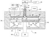
图3是根据本发明的一个实施例的用于沉积非晶和微晶膜的处理室300的示意性横截面图。在一个实施例中,室300包括壁302、底部304、喷头310、和衬底支撑件330,这些部件共同限定处理区域306。处理区域306可经由阀308访问,以使得衬底102可以被传送进出室300。衬底支撑件330包括用于支撑衬底102的衬底接收表面332以及连接到举升系统336的杆334,举升系统336构造成升高和降低衬底支撑件330。遮蔽框架333可以可选地被放置在衬底102的边缘上。举升销338可移动地设置成穿过衬底支撑件330以使得衬底102移动到达和离开衬底接收表面332。衬底支撑件330还可以包括加热和/或冷却元件330以将衬底支撑件330保持在期望的温度。衬底支撑件330还可以包括接地带331以在衬底支撑件330的边缘上提供RF接地。Figure 3 is a schematic cross-sectional view of a
喷头310在其边缘处通过悬挂件314连接到背板312。喷头310还可以通过一个或多个中心支撑件316连接到背板,以帮助防止中间下垂和/或控制喷头310的平直度/弯曲度。气体源320构造成供应处理气体(含硅气体)穿过气体供给管345。在一个实施例中,气体供给管345是构造成将处理气体穿过喷头310中的多个气体通道311供给到处理区域306的环形管。
氢气源390流体连接到远程等离子体源324(例如电感耦合远程等离子体源)。远程等离子体源324还经过视线管347和中央供给管349而流体连接到处理区域306。视线管347将远程等离子体源324流体连接到中央供给管349。本文使用的术语“视线”是为了表示远程等离子体源324和处理室300之间的短距离以使得可能的氢自由基重组或吸附在管的表面上最小化。在一个实施例中,视线管347提供用于氢自由基的直接路径,其中没有任意尖锐弯曲。在一个实施例中,视线管347提供用于氢自由基的直接路径,其中没有任意弯曲。视线管347包括由惰性材料(例如,蓝宝石、石英或其他陶瓷材料)制成的管,以防止由远程等离子体源324提供的氢自由基被吸附和/或重组。此外,可以提供加热器套351,以进一步防止由远程等离子体源324提供的氢自由基在传送到处理区域306中之前被吸附和/或重组。视线管347和中央供给管349构造成为在远程等离子体源324中产生的氢自由基提供到达处理区域306中的直接的短路径。在一个实施例中,如图3所示,中央供给管349构造成将在远程等离子体源324中产生的氢自由基直接传送经过喷头310中的中央开口353而到达处理区域306中。A
在一个实施例中,处理室300还包括清洁气体远程等离子体源395,清洁气体远程等离子体源395流体连接到位于喷头310后方的气体室397,并且还经过形成于喷头310中的气体通道311而连接到处理区域306。清洁气体远程等离子体源395连接到清洁气体源396,清洁气体源396能够将清洁气体传送到清洁气体远程等离子体源395,以使得能够形成具有能量的清洁气体以在沉积处理之间清洁喷头310和其他腔室组件的表面。通常的清洁气体包括含卤素气体(例如NF3、F2、Cl2、或其他气体),这些气体用于在沉积处理之前的时间段中去除形成于腔室组件上的部分的沉积材料。应理解,如图3所示,尽管一般需要定位清洁气体远程等离子体源395的出口398以确保喷头310和腔室组件的表面可以在腔室清洁处理期间被有效地清洁,但是根据本发明的实施例这一般不是在沉积处理期间传输供使用的氢自由基的有利位置。如图3所示,出口398的位置一般不利于将氢自由基引入到处理区域306中,因为很可能通过形成的氢自由基和从处理气体源320传输的前驱体气体的反应而在气体室397中形成气相颗粒,这将在喷头310后方和内部提供不期望的沉积。In one embodiment, the
图4是根据另一实施例的用于分别将来自远程等离子体源324的氢自由基和来自处理气体源320的处理气体输送到处理室300的处理区域306中的喷头410的示意性横截面图。在本实施例中,中央供给管349流体连接到喷头410内的内部区域405。内部区域405转而流体连接到多个通道412,多个通道412将喷头410的内部区域405流体连接到处理室300的处理区域306。在此构造中,氢自由基被从远程等离子体源324传送经过视线管347和中央供给管349而进入到喷头410的内部区域405中。从这里,氢自由基穿过多个通道412被平均地分配到处理区域306中。同时,处理气体(例如硅烷)被从气体源320传送经过气体供给管345并经过喷头410中的多个气体通道311而进入到处理区域306中。4 is a schematic cross-section of a
RF功率源322耦接到背板312和/或喷头310、410,以向喷头310、410提供RF功率,以使得在喷头310、410与衬底支撑件330或室壁302之间产生电场。因此,在处理区域306中产生电容耦合等离子体以用于在衬底102上沉积膜。真空泵309也经由节流阀380连接到处理室300以将处理区域306控制在期望的压力下。An
不考虑具体实施例,气体源320、远程等离子体源324和喷头310、410构造成使得在远程等离子体源324中产生的氢自由基只在处理区域306中被引导到处理气体,以防止在处理室300的其他区域中不期望的混合和不期望的沉积。此外,氢自由基被直接传送到处理区域306中以使得氢原子在与设置在处理区域306中的处理气体混合之前的重组或能量损失最小化。因此,使不期望的Si-H2键最小化,并且使期望的Si-H键最大化,以提供更有效的硅膜沉积。Regardless of the particular embodiment, the
在一个实施例中,氢自由基在一个或多个远程等离子体源(例如图3和图4所示的远程等离子体源324)内产生。在一个实施例中,氢自由基从直接连接到处理区域306的单一远程等离子体源产生。在另一实施例中,氢自由基从各自直接连接到处理区域306的多个远程等离子体源产生。在一个实施例中,多个远程等离子体源324沿着喷头310、410均匀地间隔开,以使得通过控制来自均匀间隔开的远程等离子体源324中每一者的气体流率和远程等离子体源功率,可以将均匀的氢自由基流动传送至处理区域306中。在另一实施例中,多个远程等离子体源324沿着喷头310间隔开呈期望的图案并以期望的方式受到控制,以将非均匀的氢自由基流动提供至处理区域306中以改善沉积处理结果的某些方面。在一个实施例中,根据在处理室300中处理的衬底102的尺寸,一个或多个远程等离子体源可以具有从约10kW到约40kW或更大的额定功率输出。在一个实施例中,使用约14W/cm2到约18W/cm2之间的RF功率。In one embodiment, hydrogen radicals are generated within one or more remote plasma sources (eg,
图5示出工艺步骤500的示例,工艺步骤500用于例如在开始沉积处理时开始在远程等离子体源324中形成氢自由基。在一个实施例中,首先在框510处建立到远程等离子体源324的氩气流率。在一个实施例中,氩气流率设置在约400sccm/L到约750sccm/L之间。在框520,氩气在远程等离子体源内被激发成等离子体,并且处理室300中的节流阀380被打开。然后,在框530,以约0.4sccm/L/s到约40sccm/L/s之间的流率将氢气供应到远程等离子体源324。氢气的流率可以连续地升高而达到约40sccm/L到约205sccm/L之间的稳态流动。在框540,氩气的流动的流率从约0.4sccm/L/s降低到约17sccm/L/s,直到氩气的流动达到期望点以使得在远程等离子体源324的出口处存在氢自由基的稳定流为止。在一个实施例中,氩气的流动例如当在从约0.1Torr到约1Torr的处理室压力下使用时下降到零。在另一实施例中,氩气的流动例如当在高于约1Torr的处理室压力下使用时持续处于低流率仅用于维持产生氢自由基。FIG. 5 shows an example of a
在一个实施例中,当在衬底102上所执行的沉积处理期间处理室300的处理区域306中的成分和/或压力变化时,期望调节输送到远程等离子体源324中的等离子体产生区域的压力、气体流率和/或气体的比率(例如载气(例如氩气)与氢的比率),以防止在该处产生的等离子体消失。In one embodiment, as the composition and/or pressure in the
下面提供根据本发明的用于使用图3和图4的处理室300来形成图1和图2的太阳能电池100和200中包含的非晶和微晶硅层的沉积方法的示例。向处理室300提供表面积为10,000cm2或更大的衬底,优选为40,000cm2或更大,更加优选地为55,000cm2或更大。An example of a deposition method for forming the amorphous and microcrystalline silicon layers included in the
在一个实施例中,设置加热和/或冷却元件339以在沉积期间提供约400摄氏度或更低的衬底支撑温度,优选为约150摄氏度至约400摄氏度之间。设置在衬底接收表面332上的衬底102的上表面与喷头310、410在沉积期间的间距可以在约200mil到约1,000mil之间。In one embodiment, heating and/or
为沉积硅膜,一般通过气体源320来提供硅基气体。使得的硅基气体包括但不限于硅烷(SiH4)、乙硅烷(Si2H6)、四氟化硅(SiF4)、四氯化硅(SiCl4)、二氯甲硅烷(SiH2Cl2)及其组合。p型层的p型掺杂剂可以各自包括第III族元素,例如硼或铝。含硼来源的示例包括三甲基硼(TMB)、乙硼烷(B2H6)和类似化合物。n型硅层的n型掺杂剂可以各自包括第V族元素,例如磷、砷或锑。含磷来源的示例包括磷化氢和类似化合物。通常利用载气(例如氢、氩、氦和其他适合的化合物)来提供掺杂剂。To deposit a silicon film, a silicon-based gas is typically provided by
下面举例说明根据本发明的实施例可以用于在图3和图4所示的一个或多个处理室300中形成串联电池(例如图2中所示的太阳能电池200)的工艺步骤的示例。在一个实施例中,在一个处理室300中接收上面沉积有前TCO层110的衬底102。通过从气体源320以约1sccm/L到约10sccm/L之间的流率提供硅烷气体并使该硅烷气体经过气体供给管345并经过喷头310、410中的多个气体通道311而进入到处理区域306中,可以在衬底102上形成p型非晶硅层122。同时,根据上文参照图5提供的描述在远程等离子体源324中产生的氢自由基被提供经过视线管347、中央供给管349以及喷头310、410而进入到处理区域306中。可以以约0.005sccm/L到约0.05sccm/L之间的流率与硅烷一起提供三甲基硼。也可以以约1sccm/L到约15sccm/L之间的流率提供甲烷。可以向喷头310、410提供约15mW/cm2到约200mW/cm2之间的RF功率以在处理区域306(图3)中在衬底102的表面上方形成等离子体。在衬底102上方形成的等离子体包括被输送经过喷头310、410的硅烷气体和从远程等离子体源324输送的氢自由基。处理室300的压力可以被维持在约0.1Torr到约20Torr之间,优选在约1Torr到约4Torr之间。The following illustrates examples of process steps that may be used to form tandem cells, such as
然后,衬底102可以被传送到与处理室300类似地构造的另一处理室中,以在p型非晶硅层122上沉积本征型非晶硅层124。在一个实施例中,硅烷气体被从气体源320以约0.5sccm/L到约7sccm/L之间的流率提供,经过气体供给管345并经过喷头310、410中的多个气体通道311而到达处理区域306中。同时,根据上文参照图5提供的描述在远程等离子体源324中产生的氢自由基被提供经过视线管347、中央供给管349以及喷头310、410而进入到处理区域306中。可以向喷头310、410提供约15mW/cm2到约250mW/cm2之间的RF功率以将能量传输给处理区域306中的硅烷和氢自由基混合物。处理室300的压力可以被维持在约0.5Torr到约5Torr之间。
然后,在衬底102仍然处于处理室300中时,在本征型非晶硅层124上沉积n型微晶硅层126。在一个实施例中,硅烷气体被从气体源320以约0.1sccm/L到约0.8sccm/L之间(例如约0.35sccm/L)的流率提供,经过气体供给管345并经过喷头310、410中的多个气体通道311而到达处理区域306中。同时,根据上文参照图5提供的描述在远程等离子体源324中产生的氢自由基被提供经过视线管347、中央供给管349以及喷头310、410而进入到处理区域306中。可以以约0.0005sccm/L到约0.06sccm/L之间的流率与硅烷一起提供磷化氢。可以向喷头310、410提供约100mW/cm2到约900mW/cm2之间的RF功率以将能量传输给处理区域306中的硅烷和氢自由基混合物。处理室300的压力可以被维持在约1Torr到约100Torr之间,优选在约3Torr到约20Torr之间。Then, an n-type
然后,衬底102被移动到另一处理室300以在n型微晶硅层126上沉积p型微晶硅层132。在一个实施例中,硅烷气体被从气体源320以约0.1sccm/L到约0.8sccm/L之间的流率提供,经过气体供给管345并经过喷头310、410中的多个气体通道311而到达处理区域306中。同时,根据上文参照图5提供的描述在远程等离子体源324中产生的氢自由基被提供经过视线管347、中央供给管349以及喷头310、410而进入到处理区域306中。可以以约0.0002sccm/L到约0.0016sccm/L之间的流率与硅烷一起提供三甲基硼。可以向喷头310、410提供约50mW/cm2到约700mW/cm2之间的RF功率以将能量传输给处理区域306中的硅烷和氢自由基混合物。处理室300的压力可以被维持在约1Torr到约100Torr之间,优选在约3Torr到约20Torr之间。The
然后,衬底102被传送到另一处理室300中以在p型微晶硅层132上沉积本征型微晶硅种子层133。在一个实施例中,硅烷气体经过从约20秒到约300秒(例如在约40秒到约240秒之间)的时间段而逐渐从零点提高到第二设定点(例如在约2.8sccm/L到约5.6sccm/L之间)。提高的硅烷流被从气体源320提供,经过气体供给管345并经过喷头310、410中的多个气体通道311而到达处理区域306中。同时,根据上文参照图5提供的描述在远程等离子体源324中产生的氢自由基被提供经过视线管347、中央供给管349以及喷头310、410而进入到处理区域306中。RF功率也可以与硅烷流类似地从约0瓦特/cm2提高到约2瓦特/cm2,以将能量传输给处理区域306中的硅烷和氢自由基混合物。处理室300的压力可以被维持在约1Torr到约12Torr之间。Then, the
认为在形成本征型微晶硅种子层133中硅烷流的逐渐提高有助于硅原子均匀地粘附和分布在衬底102的表面上,从而形成具有期望的膜特性的本征型微晶硅种子层133。硅原子在衬底102的表面上的均匀粘附提供良好的成核位置,以用于后来的原子在该位置上成核。形成于衬底102上的均匀成核位置提高后续形成于衬底102上的膜的结晶性。因此,到处理区域306中的硅烷流的逐渐提高使得解离的硅原子能够具有充足的时间来被逐渐吸收在衬底102的表面上,从而提供具有均匀分布硅原子的表面,该表面提供成核位置,这促进后续沉积的层的改进的结晶性。It is believed that the gradual increase in silane flow in forming the intrinsic type microcrystalline silicon seed layer 133 helps the silicon atoms to adhere and distribute uniformly on the surface of the
然后,在处理室300中在本征型微晶硅种子层133上沉积本征型微晶硅层134。硅烷气体被从气体源320以约0.1sccm/L到约0.8sccm/L之间的流率提供,经过气体供给管345并经过喷头310、410中的多个气体通道311而到达处理区域306中。同时,根据上文参照图5提供的描述在远程等离子体源324中产生的氢自由基被提供经过视线管347、中央供给管349以及喷头310、410而进入到处理区域306中。可以向喷头310、410提供约300mW/cm2或更大(优选为600mW/cm2或更大)的RF功率以将能量传输给处理区域306中的硅烷和氢自由基混合物。处理室300的压力可以被维持在约1Torr到约100Torr之间,优选在约3Torr到约20Torr之间。Then, an intrinsic type microcrystalline silicon layer 134 is deposited on the intrinsic type microcrystalline silicon seed layer 133 in the
最后,在衬底仍然位于处理室300中时,在衬底201上的本征型微晶硅层124上沉积n型非晶硅层126。在一个实施例中,可以通过首先以第一硅烷流率沉积可选的第一n型非晶硅层、然后以低于第一硅烷流率的第二硅烷流率在第一可选的n型非晶硅层上沉积第二n型非晶硅层,来沉积n型非晶硅层136。可以通过从气体源320以约1sccm/L到约10sccm/L之间(例如约5.5sccm/L)的流率提供硅烷气体并使该硅烷气体经过气体供给管345并经过喷头310、410中的多个气体通道311而进入到处理区域306中,来沉积第一可选的n型非晶硅层。同时,根据上文参照图5提供的描述在远程等离子体源324中产生的氢自由基被提供经过视线管347、中央供给管349以及喷头310、410而进入到处理区域306中。可以以约0.0005sccm/L到约0.0015sccm/L之间(例如0.0095sccm/L)的流率与硅烷一起提供磷化氢。可以向喷头310、410提供约25mW/cm2到约250mW/cm2之间的RF功率以将能量传输给处理区域306中的硅烷和氢自由基混合物。处理室300的压力可以被维持在约0.1Torr到约20Torr之间,优选在约0.5Torr到约4Torr之间。Finally, an n-type
第二n型非晶硅层沉积可以包括从气体源320以约0.1sccm/L到约5sccm/L之间(例如约0.5sccm/L到约3sccm/L之间(例如约1.42sccm/L))的流率提供硅烷气体并使该硅烷气体经过气体供给管345并经过喷头310、410中的多个气体通道311而进入到处理区域306中。同时,根据上文参照图5提供的描述在远程等离子体源324中产生的氢自由基被提供经过视线管347、中央供给管349以及喷头310、410而进入到处理区域306中。可以以约0.01sccm/L到约0.075sccm/L之间(例如约0.015sccm/L到约0.03sccm/L之间(例如约0.023sccm/L))的流率提供磷化氢。可以向喷头310、410提供约25mW/cm2到约250mW/cm2之间(例如60mW/cm2)的RF功率以将能量传输给处理区域306中的硅烷和氢自由基混合物。处理室300的压力可以被维持在约0.1Torr到约20Torr之间,优选在约0.5Torr到约4Torr之间,例如约1.5Torr。Deposition of the second n-type amorphous silicon layer may comprise from
因此,根据本发明的实施例可以通过在远程等离子体源中产生氢自由基并将氢自由基直接传输到处理室的处理区域中以与含硅气体结合来提供在太阳能电池中每个含硅层。直接就爱那个氢自由基提供到处理区域中以与含硅气体反应会产生超过现有技术沉积方法的改进的键合结构、沉积效率和沉积膜稳定性。Therefore, embodiments according to the present invention may provide hydrogen radicals in each silicon-containing layer. Providing hydrogen radicals directly into the processing region to react with the silicon-containing gas results in improved bonding structure, deposition efficiency and deposited film stability over prior art deposition methods.
尽管上文涉及本发明的实施例,但是在不脱离本发明的基本范围的情况下可以获得本发明的其他和进一步的实施例。While the above relates to embodiments of the invention, other and further embodiments of the invention can be obtained without departing from the basic scope of the invention.
Claims (20)
Applications Claiming Priority (1)
| Application Number | Priority Date | Filing Date | Title |
|---|---|---|---|
| PCT/CN2010/000325WO2011113177A1 (en) | 2010-03-17 | 2010-03-17 | Method and apparatus for remote plasma source assisted silicon-containing film deposition |
Publications (1)
| Publication Number | Publication Date |
|---|---|
| CN102892922Atrue CN102892922A (en) | 2013-01-23 |
Family
ID=44647572
Family Applications (1)
| Application Number | Title | Priority Date | Filing Date |
|---|---|---|---|
| CN2010800655041APendingCN102892922A (en) | 2010-03-17 | 2010-03-17 | Method and apparatus for remote plasma source assisted silicon-containing film deposition |
Country Status (4)
| Country | Link |
|---|---|
| US (2) | US20130012030A1 (en) |
| KR (1) | KR20130055582A (en) |
| CN (1) | CN102892922A (en) |
| WO (1) | WO2011113177A1 (en) |
Cited By (29)
| Publication number | Priority date | Publication date | Assignee | Title |
|---|---|---|---|---|
| CN104233227A (en)* | 2014-09-23 | 2014-12-24 | 上海华力微电子有限公司 | Atomic layer deposition equipment and method |
| CN107400877A (en)* | 2013-10-24 | 2017-11-28 | 朗姆研究公司 | The ground state hydroperoxyl radical source of the chemical vapor deposition of siliceous carbon film |
| CN108461374A (en)* | 2016-12-19 | 2018-08-28 | 朗姆研究公司 | Chamber conditioning for remote plasma processing |
| US10472714B2 (en) | 2013-05-31 | 2019-11-12 | Novellus Systems, Inc. | Method to obtain SiC class of films of desired composition and film properties |
| US10573522B2 (en) | 2016-08-16 | 2020-02-25 | Lam Research Corporation | Method for preventing line bending during metal fill process |
| US10580690B2 (en) | 2016-11-23 | 2020-03-03 | Lam Research Corporation | Staircase encapsulation in 3D NAND fabrication |
| US10580654B2 (en) | 2015-05-18 | 2020-03-03 | Lam Research Corporation | Feature fill with multi-stage nucleation inhibition |
| US10760158B2 (en) | 2017-12-15 | 2020-09-01 | Lam Research Corporation | Ex situ coating of chamber components for semiconductor processing |
| US10832904B2 (en) | 2012-06-12 | 2020-11-10 | Lam Research Corporation | Remote plasma based deposition of oxygen doped silicon carbide films |
| US10840087B2 (en) | 2018-07-20 | 2020-11-17 | Lam Research Corporation | Remote plasma based deposition of boron nitride, boron carbide, and boron carbonitride films |
| CN112424905A (en)* | 2018-07-09 | 2021-02-26 | 朗姆研究公司 | RF signal source supplying Radio Frequency (RF) plasma generator and remote plasma generator |
| US11049716B2 (en) | 2015-04-21 | 2021-06-29 | Lam Research Corporation | Gap fill using carbon-based films |
| US11075115B2 (en) | 2009-08-04 | 2021-07-27 | Novellus Systems, Inc. | Tungsten feature fill |
| US11264234B2 (en) | 2012-06-12 | 2022-03-01 | Novellus Systems, Inc. | Conformal deposition of silicon carbide films |
| CN114196945A (en)* | 2021-12-16 | 2022-03-18 | 江苏鲁汶仪器有限公司 | Method for reducing particles generated in PECVD film deposition process |
| CN114556518A (en)* | 2019-09-30 | 2022-05-27 | 朗姆研究公司 | Selective graphene deposition using remote plasma |
| US11410883B2 (en) | 2009-08-04 | 2022-08-09 | Novellus Systems, Inc. | Tungsten feature fill with nucleation inhibition |
| US11437269B2 (en) | 2012-03-27 | 2022-09-06 | Novellus Systems, Inc. | Tungsten feature fill with nucleation inhibition |
| CN115595561A (en)* | 2022-10-31 | 2023-01-13 | 胡倩(Cn) | Plasma enhanced atomic layer deposition equipment and deposition method |
| US11761079B2 (en) | 2017-12-07 | 2023-09-19 | Lam Research Corporation | Oxidation resistant protective layer in chamber conditioning |
| US11848199B2 (en) | 2018-10-19 | 2023-12-19 | Lam Research Corporation | Doped or undoped silicon carbide deposition and remote hydrogen plasma exposure for gapfill |
| US11901227B2 (en) | 2014-09-30 | 2024-02-13 | Lam Research Corporation | Feature fill with nucleation inhibition |
| US11920239B2 (en) | 2015-03-26 | 2024-03-05 | Lam Research Corporation | Minimizing radical recombination using ALD silicon oxide surface coating with intermittent restoration plasma |
| US11978666B2 (en) | 2018-12-05 | 2024-05-07 | Lam Research Corporation | Void free low stress fill |
| US12261081B2 (en) | 2019-02-13 | 2025-03-25 | Lam Research Corporation | Tungsten feature fill with inhibition control |
| US12334332B2 (en) | 2012-06-12 | 2025-06-17 | Lam Research Corporation | Remote plasma based deposition of silicon carbide films using silicon-containing and carbon-containing precursors |
| US12359311B2 (en) | 2012-06-12 | 2025-07-15 | Lam Research Corporation | Conformal deposition of silicon carbide films using heterogeneous precursor interaction |
| US12371781B2 (en) | 2018-10-19 | 2025-07-29 | Lam Research Corporation | In situ protective coating of chamber components for semiconductor processing |
| US12444651B2 (en) | 2022-06-28 | 2025-10-14 | Novellus Systems, Inc. | Tungsten feature fill with nucleation inhibition |
Families Citing this family (103)
| Publication number | Priority date | Publication date | Assignee | Title |
|---|---|---|---|---|
| US8291857B2 (en) | 2008-07-03 | 2012-10-23 | Applied Materials, Inc. | Apparatuses and methods for atomic layer deposition |
| US9324576B2 (en) | 2010-05-27 | 2016-04-26 | Applied Materials, Inc. | Selective etch for silicon films |
| US10283321B2 (en) | 2011-01-18 | 2019-05-07 | Applied Materials, Inc. | Semiconductor processing system and methods using capacitively coupled plasma |
| US8828859B2 (en)* | 2011-02-11 | 2014-09-09 | Semiconductor Energy Laboratory Co., Ltd. | Method for forming semiconductor film and method for manufacturing semiconductor device |
| US9064815B2 (en) | 2011-03-14 | 2015-06-23 | Applied Materials, Inc. | Methods for etch of metal and metal-oxide films |
| US8999856B2 (en) | 2011-03-14 | 2015-04-07 | Applied Materials, Inc. | Methods for etch of sin films |
| US9303318B2 (en)* | 2011-10-20 | 2016-04-05 | Applied Materials, Inc. | Multiple complementary gas distribution assemblies |
| KR101473403B1 (en) | 2011-12-28 | 2014-12-17 | 엘아이지에이디피 주식회사 | Shower head assembly and apparatus for chemical vapor deposition having the same |
| US9267739B2 (en) | 2012-07-18 | 2016-02-23 | Applied Materials, Inc. | Pedestal with multi-zone temperature control and multiple purge capabilities |
| US9373517B2 (en) | 2012-08-02 | 2016-06-21 | Applied Materials, Inc. | Semiconductor processing with DC assisted RF power for improved control |
| US9132436B2 (en) | 2012-09-21 | 2015-09-15 | Applied Materials, Inc. | Chemical control features in wafer process equipment |
| US20140099794A1 (en)* | 2012-09-21 | 2014-04-10 | Applied Materials, Inc. | Radical chemistry modulation and control using multiple flow pathways |
| US10256079B2 (en) | 2013-02-08 | 2019-04-09 | Applied Materials, Inc. | Semiconductor processing systems having multiple plasma configurations |
| US9362130B2 (en) | 2013-03-01 | 2016-06-07 | Applied Materials, Inc. | Enhanced etching processes using remote plasma sources |
| US9773648B2 (en) | 2013-08-30 | 2017-09-26 | Applied Materials, Inc. | Dual discharge modes operation for remote plasma |
| JP5764228B1 (en)* | 2014-03-18 | 2015-08-12 | 株式会社日立国際電気 | Substrate processing apparatus, semiconductor device manufacturing method, program, and recording medium |
| US9299537B2 (en) | 2014-03-20 | 2016-03-29 | Applied Materials, Inc. | Radial waveguide systems and methods for post-match control of microwaves |
| US9903020B2 (en) | 2014-03-31 | 2018-02-27 | Applied Materials, Inc. | Generation of compact alumina passivation layers on aluminum plasma equipment components |
| US10741365B2 (en)* | 2014-05-05 | 2020-08-11 | Lam Research Corporation | Low volume showerhead with porous baffle |
| US9309598B2 (en) | 2014-05-28 | 2016-04-12 | Applied Materials, Inc. | Oxide and metal removal |
| US20150348755A1 (en)* | 2014-05-29 | 2015-12-03 | Charm Engineering Co., Ltd. | Gas distribution apparatus and substrate processing apparatus including same |
| US9496167B2 (en) | 2014-07-31 | 2016-11-15 | Applied Materials, Inc. | Integrated bit-line airgap formation and gate stack post clean |
| US9613822B2 (en) | 2014-09-25 | 2017-04-04 | Applied Materials, Inc. | Oxide etch selectivity enhancement |
| US9355922B2 (en) | 2014-10-14 | 2016-05-31 | Applied Materials, Inc. | Systems and methods for internal surface conditioning in plasma processing equipment |
| US9966240B2 (en) | 2014-10-14 | 2018-05-08 | Applied Materials, Inc. | Systems and methods for internal surface conditioning assessment in plasma processing equipment |
| US11637002B2 (en) | 2014-11-26 | 2023-04-25 | Applied Materials, Inc. | Methods and systems to enhance process uniformity |
| US10573496B2 (en) | 2014-12-09 | 2020-02-25 | Applied Materials, Inc. | Direct outlet toroidal plasma source |
| US10224210B2 (en) | 2014-12-09 | 2019-03-05 | Applied Materials, Inc. | Plasma processing system with direct outlet toroidal plasma source |
| US11257693B2 (en) | 2015-01-09 | 2022-02-22 | Applied Materials, Inc. | Methods and systems to improve pedestal temperature control |
| US9728437B2 (en) | 2015-02-03 | 2017-08-08 | Applied Materials, Inc. | High temperature chuck for plasma processing systems |
| US20160225652A1 (en) | 2015-02-03 | 2016-08-04 | Applied Materials, Inc. | Low temperature chuck for plasma processing systems |
| US9881805B2 (en) | 2015-03-02 | 2018-01-30 | Applied Materials, Inc. | Silicon selective removal |
| US9691645B2 (en) | 2015-08-06 | 2017-06-27 | Applied Materials, Inc. | Bolted wafer chuck thermal management systems and methods for wafer processing systems |
| US9741593B2 (en) | 2015-08-06 | 2017-08-22 | Applied Materials, Inc. | Thermal management systems and methods for wafer processing systems |
| US9349605B1 (en) | 2015-08-07 | 2016-05-24 | Applied Materials, Inc. | Oxide etch selectivity systems and methods |
| US10504700B2 (en) | 2015-08-27 | 2019-12-10 | Applied Materials, Inc. | Plasma etching systems and methods with secondary plasma injection |
| US10444892B2 (en)* | 2015-10-07 | 2019-10-15 | Microchip Technology Incorporated | Capacitance measurement device with reduced noise |
| US10522371B2 (en) | 2016-05-19 | 2019-12-31 | Applied Materials, Inc. | Systems and methods for improved semiconductor etching and component protection |
| US10504754B2 (en) | 2016-05-19 | 2019-12-10 | Applied Materials, Inc. | Systems and methods for improved semiconductor etching and component protection |
| US9865484B1 (en) | 2016-06-29 | 2018-01-09 | Applied Materials, Inc. | Selective etch using material modification and RF pulsing |
| US10062575B2 (en) | 2016-09-09 | 2018-08-28 | Applied Materials, Inc. | Poly directional etch by oxidation |
| US10629473B2 (en) | 2016-09-09 | 2020-04-21 | Applied Materials, Inc. | Footing removal for nitride spacer |
| US9934942B1 (en) | 2016-10-04 | 2018-04-03 | Applied Materials, Inc. | Chamber with flow-through source |
| US10546729B2 (en) | 2016-10-04 | 2020-01-28 | Applied Materials, Inc. | Dual-channel showerhead with improved profile |
| US10062585B2 (en) | 2016-10-04 | 2018-08-28 | Applied Materials, Inc. | Oxygen compatible plasma source |
| US10062579B2 (en) | 2016-10-07 | 2018-08-28 | Applied Materials, Inc. | Selective SiN lateral recess |
| US9947549B1 (en) | 2016-10-10 | 2018-04-17 | Applied Materials, Inc. | Cobalt-containing material removal |
| US10163696B2 (en) | 2016-11-11 | 2018-12-25 | Applied Materials, Inc. | Selective cobalt removal for bottom up gapfill |
| US9768034B1 (en) | 2016-11-11 | 2017-09-19 | Applied Materials, Inc. | Removal methods for high aspect ratio structures |
| US10242908B2 (en) | 2016-11-14 | 2019-03-26 | Applied Materials, Inc. | Airgap formation with damage-free copper |
| US10026621B2 (en) | 2016-11-14 | 2018-07-17 | Applied Materials, Inc. | SiN spacer profile patterning |
| CN109964303B (en) | 2016-11-18 | 2023-08-29 | 应用材料公司 | Method for depositing an amorphous silicon layer or a silicon oxycarbide layer via physical vapor deposition |
| US10566206B2 (en) | 2016-12-27 | 2020-02-18 | Applied Materials, Inc. | Systems and methods for anisotropic material breakthrough |
| US10431429B2 (en) | 2017-02-03 | 2019-10-01 | Applied Materials, Inc. | Systems and methods for radial and azimuthal control of plasma uniformity |
| US10403507B2 (en) | 2017-02-03 | 2019-09-03 | Applied Materials, Inc. | Shaped etch profile with oxidation |
| US10043684B1 (en) | 2017-02-06 | 2018-08-07 | Applied Materials, Inc. | Self-limiting atomic thermal etching systems and methods |
| US10319739B2 (en) | 2017-02-08 | 2019-06-11 | Applied Materials, Inc. | Accommodating imperfectly aligned memory holes |
| US10943834B2 (en) | 2017-03-13 | 2021-03-09 | Applied Materials, Inc. | Replacement contact process |
| US10319649B2 (en) | 2017-04-11 | 2019-06-11 | Applied Materials, Inc. | Optical emission spectroscopy (OES) for remote plasma monitoring |
| JP7176860B6 (en) | 2017-05-17 | 2022-12-16 | アプライド マテリアルズ インコーポレイテッド | Semiconductor processing chamber to improve precursor flow |
| US11276559B2 (en) | 2017-05-17 | 2022-03-15 | Applied Materials, Inc. | Semiconductor processing chamber for multiple precursor flow |
| US11276590B2 (en) | 2017-05-17 | 2022-03-15 | Applied Materials, Inc. | Multi-zone semiconductor substrate supports |
| US10497579B2 (en) | 2017-05-31 | 2019-12-03 | Applied Materials, Inc. | Water-free etching methods |
| US10049891B1 (en) | 2017-05-31 | 2018-08-14 | Applied Materials, Inc. | Selective in situ cobalt residue removal |
| US10920320B2 (en) | 2017-06-16 | 2021-02-16 | Applied Materials, Inc. | Plasma health determination in semiconductor substrate processing reactors |
| US10541246B2 (en) | 2017-06-26 | 2020-01-21 | Applied Materials, Inc. | 3D flash memory cells which discourage cross-cell electrical tunneling |
| US10727080B2 (en) | 2017-07-07 | 2020-07-28 | Applied Materials, Inc. | Tantalum-containing material removal |
| US10541184B2 (en) | 2017-07-11 | 2020-01-21 | Applied Materials, Inc. | Optical emission spectroscopic techniques for monitoring etching |
| US10354889B2 (en) | 2017-07-17 | 2019-07-16 | Applied Materials, Inc. | Non-halogen etching of silicon-containing materials |
| US10043674B1 (en) | 2017-08-04 | 2018-08-07 | Applied Materials, Inc. | Germanium etching systems and methods |
| US10170336B1 (en) | 2017-08-04 | 2019-01-01 | Applied Materials, Inc. | Methods for anisotropic control of selective silicon removal |
| US10297458B2 (en) | 2017-08-07 | 2019-05-21 | Applied Materials, Inc. | Process window widening using coated parts in plasma etch processes |
| US10128086B1 (en) | 2017-10-24 | 2018-11-13 | Applied Materials, Inc. | Silicon pretreatment for nitride removal |
| US10283324B1 (en) | 2017-10-24 | 2019-05-07 | Applied Materials, Inc. | Oxygen treatment for nitride etching |
| US10256112B1 (en) | 2017-12-08 | 2019-04-09 | Applied Materials, Inc. | Selective tungsten removal |
| US10903054B2 (en) | 2017-12-19 | 2021-01-26 | Applied Materials, Inc. | Multi-zone gas distribution systems and methods |
| US11328909B2 (en) | 2017-12-22 | 2022-05-10 | Applied Materials, Inc. | Chamber conditioning and removal processes |
| US10854426B2 (en) | 2018-01-08 | 2020-12-01 | Applied Materials, Inc. | Metal recess for semiconductor structures |
| US10636626B2 (en) | 2018-01-25 | 2020-04-28 | Applied Materials, Inc. | Dogbone inlet cone profile for remote plasma oxidation chamber |
| US10679870B2 (en) | 2018-02-15 | 2020-06-09 | Applied Materials, Inc. | Semiconductor processing chamber multistage mixing apparatus |
| US10964512B2 (en) | 2018-02-15 | 2021-03-30 | Applied Materials, Inc. | Semiconductor processing chamber multistage mixing apparatus and methods |
| TWI766433B (en) | 2018-02-28 | 2022-06-01 | 美商應用材料股份有限公司 | Systems and methods to form airgaps |
| US10593560B2 (en) | 2018-03-01 | 2020-03-17 | Applied Materials, Inc. | Magnetic induction plasma source for semiconductor processes and equipment |
| US10319600B1 (en) | 2018-03-12 | 2019-06-11 | Applied Materials, Inc. | Thermal silicon etch |
| US10497573B2 (en) | 2018-03-13 | 2019-12-03 | Applied Materials, Inc. | Selective atomic layer etching of semiconductor materials |
| US10573527B2 (en) | 2018-04-06 | 2020-02-25 | Applied Materials, Inc. | Gas-phase selective etching systems and methods |
| US10490406B2 (en) | 2018-04-10 | 2019-11-26 | Appled Materials, Inc. | Systems and methods for material breakthrough |
| US10699879B2 (en) | 2018-04-17 | 2020-06-30 | Applied Materials, Inc. | Two piece electrode assembly with gap for plasma control |
| US10886137B2 (en) | 2018-04-30 | 2021-01-05 | Applied Materials, Inc. | Selective nitride removal |
| US10872778B2 (en) | 2018-07-06 | 2020-12-22 | Applied Materials, Inc. | Systems and methods utilizing solid-phase etchants |
| US10755941B2 (en) | 2018-07-06 | 2020-08-25 | Applied Materials, Inc. | Self-limiting selective etching systems and methods |
| US10672642B2 (en) | 2018-07-24 | 2020-06-02 | Applied Materials, Inc. | Systems and methods for pedestal configuration |
| US11049755B2 (en) | 2018-09-14 | 2021-06-29 | Applied Materials, Inc. | Semiconductor substrate supports with embedded RF shield |
| US10892198B2 (en) | 2018-09-14 | 2021-01-12 | Applied Materials, Inc. | Systems and methods for improved performance in semiconductor processing |
| US11062887B2 (en) | 2018-09-17 | 2021-07-13 | Applied Materials, Inc. | High temperature RF heater pedestals |
| US11417534B2 (en) | 2018-09-21 | 2022-08-16 | Applied Materials, Inc. | Selective material removal |
| CN110970287B (en)* | 2018-09-28 | 2022-12-02 | 长鑫存储技术有限公司 | Method for preparing amorphous silicon thin film |
| US11682560B2 (en) | 2018-10-11 | 2023-06-20 | Applied Materials, Inc. | Systems and methods for hafnium-containing film removal |
| US11121002B2 (en) | 2018-10-24 | 2021-09-14 | Applied Materials, Inc. | Systems and methods for etching metals and metal derivatives |
| US11437242B2 (en) | 2018-11-27 | 2022-09-06 | Applied Materials, Inc. | Selective removal of silicon-containing materials |
| US11721527B2 (en) | 2019-01-07 | 2023-08-08 | Applied Materials, Inc. | Processing chamber mixing systems |
| US10920319B2 (en) | 2019-01-11 | 2021-02-16 | Applied Materials, Inc. | Ceramic showerheads with conductive electrodes |
| US12421608B2 (en) | 2019-09-04 | 2025-09-23 | Gallium Enterprises Pty Ltd | RPCVD apparatus and methods for forming a film |
Citations (2)
| Publication number | Priority date | Publication date | Assignee | Title |
|---|---|---|---|---|
| CN1735710A (en)* | 2002-12-20 | 2006-02-15 | 应用材料有限公司 | Method and equipment for forming high-quality low-temperature silicon nitride film |
| WO2007140426A2 (en)* | 2006-05-30 | 2007-12-06 | Applied Materials, Inc. | Process chamber for dielectric gapfill |
Family Cites Families (2)
| Publication number | Priority date | Publication date | Assignee | Title |
|---|---|---|---|---|
| KR100725037B1 (en)* | 2005-01-21 | 2007-06-07 | 세메스 주식회사 | Semiconductor Plasma Processing Apparatus And Method |
| US20070051388A1 (en)* | 2005-09-06 | 2007-03-08 | Applied Materials, Inc. | Apparatus and methods for using high frequency chokes in a substrate deposition apparatus |
- 2010
- 2010-03-17KRKR1020127026980Apatent/KR20130055582A/ennot_activeWithdrawn
- 2010-03-17USUS13/634,526patent/US20130012030A1/ennot_activeAbandoned
- 2010-03-17WOPCT/CN2010/000325patent/WO2011113177A1/enactiveApplication Filing
- 2010-03-17CNCN2010800655041Apatent/CN102892922A/enactivePending
- 2010-05-04USUS12/773,497patent/US20110230008A1/ennot_activeAbandoned
Patent Citations (2)
| Publication number | Priority date | Publication date | Assignee | Title |
|---|---|---|---|---|
| CN1735710A (en)* | 2002-12-20 | 2006-02-15 | 应用材料有限公司 | Method and equipment for forming high-quality low-temperature silicon nitride film |
| WO2007140426A2 (en)* | 2006-05-30 | 2007-12-06 | Applied Materials, Inc. | Process chamber for dielectric gapfill |
Cited By (47)
| Publication number | Priority date | Publication date | Assignee | Title |
|---|---|---|---|---|
| US11075115B2 (en) | 2009-08-04 | 2021-07-27 | Novellus Systems, Inc. | Tungsten feature fill |
| US11410883B2 (en) | 2009-08-04 | 2022-08-09 | Novellus Systems, Inc. | Tungsten feature fill with nucleation inhibition |
| US11437269B2 (en) | 2012-03-27 | 2022-09-06 | Novellus Systems, Inc. | Tungsten feature fill with nucleation inhibition |
| US12387979B2 (en) | 2012-03-27 | 2025-08-12 | Novellus Systems, Inc. | Tungsten feature fill with nucleation inhibition |
| US11894227B2 (en) | 2012-06-12 | 2024-02-06 | Novellus Systems, Inc. | Conformal deposition of silicon carbide films |
| US11264234B2 (en) | 2012-06-12 | 2022-03-01 | Novellus Systems, Inc. | Conformal deposition of silicon carbide films |
| US12359311B2 (en) | 2012-06-12 | 2025-07-15 | Lam Research Corporation | Conformal deposition of silicon carbide films using heterogeneous precursor interaction |
| US12334332B2 (en) | 2012-06-12 | 2025-06-17 | Lam Research Corporation | Remote plasma based deposition of silicon carbide films using silicon-containing and carbon-containing precursors |
| US12272547B2 (en) | 2012-06-12 | 2025-04-08 | Novellus Systems, Inc. | Conformal deposition of silicon carbide films |
| US10832904B2 (en) | 2012-06-12 | 2020-11-10 | Lam Research Corporation | Remote plasma based deposition of oxygen doped silicon carbide films |
| US11732350B2 (en) | 2013-05-31 | 2023-08-22 | Novellus Systems, Inc. | Films of desired composition and film properties |
| US11708634B2 (en) | 2013-05-31 | 2023-07-25 | Novellus Systems, Inc. | Films of desired composition and film properties |
| US11680315B2 (en) | 2013-05-31 | 2023-06-20 | Novellus Systems, Inc. | Films of desired composition and film properties |
| US10472714B2 (en) | 2013-05-31 | 2019-11-12 | Novellus Systems, Inc. | Method to obtain SiC class of films of desired composition and film properties |
| US11680314B2 (en) | 2013-05-31 | 2023-06-20 | Novellus Systems, Inc. | Films of desired composition and film properties |
| CN107400877B (en)* | 2013-10-24 | 2020-06-30 | 朗姆研究公司 | Ground state hydrogen radical source for chemical vapor deposition of silicon-containing carbon films |
| CN107400877A (en)* | 2013-10-24 | 2017-11-28 | 朗姆研究公司 | The ground state hydroperoxyl radical source of the chemical vapor deposition of siliceous carbon film |
| CN104233227A (en)* | 2014-09-23 | 2014-12-24 | 上海华力微电子有限公司 | Atomic layer deposition equipment and method |
| US11901227B2 (en) | 2014-09-30 | 2024-02-13 | Lam Research Corporation | Feature fill with nucleation inhibition |
| US11920239B2 (en) | 2015-03-26 | 2024-03-05 | Lam Research Corporation | Minimizing radical recombination using ALD silicon oxide surface coating with intermittent restoration plasma |
| US11049716B2 (en) | 2015-04-21 | 2021-06-29 | Lam Research Corporation | Gap fill using carbon-based films |
| US10580654B2 (en) | 2015-05-18 | 2020-03-03 | Lam Research Corporation | Feature fill with multi-stage nucleation inhibition |
| US10916434B2 (en) | 2015-05-18 | 2021-02-09 | Lam Research Corporation | Feature fill with multi-stage nucleation inhibition |
| US11355345B2 (en) | 2016-08-16 | 2022-06-07 | Lam Research Corporation | Method for preventing line bending during metal fill process |
| US10573522B2 (en) | 2016-08-16 | 2020-02-25 | Lam Research Corporation | Method for preventing line bending during metal fill process |
| US12362188B2 (en) | 2016-08-16 | 2025-07-15 | Lam Research Corporation | Method for preventing line bending during metal fill process |
| US10580690B2 (en) | 2016-11-23 | 2020-03-03 | Lam Research Corporation | Staircase encapsulation in 3D NAND fabrication |
| TWI769204B (en)* | 2016-12-19 | 2022-07-01 | 美商蘭姆研究公司 | Methods of chamber conditioning for remote plasma process |
| CN108461374A (en)* | 2016-12-19 | 2018-08-28 | 朗姆研究公司 | Chamber conditioning for remote plasma processing |
| CN108461374B (en)* | 2016-12-19 | 2021-06-29 | 朗姆研究公司 | Chamber Conditioning for Remote Plasma Processing |
| TWI847146B (en)* | 2016-12-19 | 2024-07-01 | 美商蘭姆研究公司 | Methods of chamber conditioning for remote plasma process |
| US11761079B2 (en) | 2017-12-07 | 2023-09-19 | Lam Research Corporation | Oxidation resistant protective layer in chamber conditioning |
| US11365479B2 (en) | 2017-12-15 | 2022-06-21 | Lam Research Corporation | Ex situ coating of chamber components for semiconductor processing |
| US10760158B2 (en) | 2017-12-15 | 2020-09-01 | Lam Research Corporation | Ex situ coating of chamber components for semiconductor processing |
| US12227837B2 (en) | 2017-12-15 | 2025-02-18 | Lam Research Corporation | Ex situ coating of chamber components for semiconductor processing |
| US12163219B2 (en) | 2017-12-15 | 2024-12-10 | Lam Research Corporation | Ex situ coating of chamber components for semiconductor processing |
| CN112424905A (en)* | 2018-07-09 | 2021-02-26 | 朗姆研究公司 | RF signal source supplying Radio Frequency (RF) plasma generator and remote plasma generator |
| US10840087B2 (en) | 2018-07-20 | 2020-11-17 | Lam Research Corporation | Remote plasma based deposition of boron nitride, boron carbide, and boron carbonitride films |
| US12300488B2 (en) | 2018-10-19 | 2025-05-13 | Lam Research Corporation | Doped or undoped silicon carbide deposition and remote hydrogen plasma exposure for gapfill |
| US11848199B2 (en) | 2018-10-19 | 2023-12-19 | Lam Research Corporation | Doped or undoped silicon carbide deposition and remote hydrogen plasma exposure for gapfill |
| US12371781B2 (en) | 2018-10-19 | 2025-07-29 | Lam Research Corporation | In situ protective coating of chamber components for semiconductor processing |
| US11978666B2 (en) | 2018-12-05 | 2024-05-07 | Lam Research Corporation | Void free low stress fill |
| US12261081B2 (en) | 2019-02-13 | 2025-03-25 | Lam Research Corporation | Tungsten feature fill with inhibition control |
| CN114556518A (en)* | 2019-09-30 | 2022-05-27 | 朗姆研究公司 | Selective graphene deposition using remote plasma |
| CN114196945A (en)* | 2021-12-16 | 2022-03-18 | 江苏鲁汶仪器有限公司 | Method for reducing particles generated in PECVD film deposition process |
| US12444651B2 (en) | 2022-06-28 | 2025-10-14 | Novellus Systems, Inc. | Tungsten feature fill with nucleation inhibition |
| CN115595561A (en)* | 2022-10-31 | 2023-01-13 | 胡倩(Cn) | Plasma enhanced atomic layer deposition equipment and deposition method |
Also Published As
| Publication number | Publication date |
|---|---|
| KR20130055582A (en) | 2013-05-28 |
| US20130012030A1 (en) | 2013-01-10 |
| US20110230008A1 (en) | 2011-09-22 |
| WO2011113177A1 (en) | 2011-09-22 |
Similar Documents
| Publication | Publication Date | Title |
|---|---|---|
| CN102892922A (en) | Method and apparatus for remote plasma source assisted silicon-containing film deposition | |
| CN101322251B (en) | Method and apparatus for depositing a microcrystalline silicon film for photovoltaic device | |
| US7582515B2 (en) | Multi-junction solar cells and methods and apparatuses for forming the same | |
| US8728918B2 (en) | Method and apparatus for fabricating silicon heterojunction solar cells | |
| US9441295B2 (en) | Multi-channel gas-delivery system | |
| CN101836299B (en) | Microcrystalline silicon deposition for thin film solar applications | |
| US20080188062A1 (en) | Method of forming microcrystalline silicon film | |
| US20100258169A1 (en) | Pulsed plasma deposition for forming microcrystalline silicon layer for solar applications | |
| US20080245414A1 (en) | Methods for forming a photovoltaic device with low contact resistance | |
| US20080223440A1 (en) | Multi-junction solar cells and methods and apparatuses for forming the same | |
| CN102534570B (en) | A method for plasma-enhanced chemical vapor deposition of microcrystalline silicon thin films | |
| CN105506583A (en) | Three-layer membrane process of tube type PECVD | |
| JPH0458173B2 (en) | ||
| CN120111987B (en) | Method and equipment for preparing oxygen-doped microcrystalline silicon thin film | |
| JPH0522376B2 (en) | ||
| US20110263074A1 (en) | Apparatus and methods for reducing light induced damage in thin film solar cells | |
| KR20110074926A (en) | Multiple gas supply device and method | |
| JP2011238925A (en) | Method of dynamically controlling film microstructure formed in microcrystalline layer |
Legal Events
| Date | Code | Title | Description |
|---|---|---|---|
| C06 | Publication | ||
| PB01 | Publication | ||
| C10 | Entry into substantive examination | ||
| SE01 | Entry into force of request for substantive examination | ||
| C02 | Deemed withdrawal of patent application after publication (patent law 2001) | ||
| WD01 | Invention patent application deemed withdrawn after publication | Application publication date:20130123 |