CN102867813A - Electronic device - Google Patents
Electronic deviceDownload PDFInfo
- Publication number
- CN102867813A CN102867813ACN2012101712752ACN201210171275ACN102867813ACN 102867813 ACN102867813 ACN 102867813ACN 2012101712752 ACN2012101712752 ACN 2012101712752ACN 201210171275 ACN201210171275 ACN 201210171275ACN 102867813 ACN102867813 ACN 102867813A
- Authority
- CN
- China
- Prior art keywords
- electromagnetic shielding
- shielding structure
- polarizer
- semiconductor
- package
- Prior art date
- Legal status (The legal status is an assumption and is not a legal conclusion. Google has not performed a legal analysis and makes no representation as to the accuracy of the status listed.)
- Granted
Links
Images


Classifications
- H—ELECTRICITY
- H01—ELECTRIC ELEMENTS
- H01L—SEMICONDUCTOR DEVICES NOT COVERED BY CLASS H10
- H01L23/00—Details of semiconductor or other solid state devices
- H01L23/48—Arrangements for conducting electric current to or from the solid state body in operation, e.g. leads, terminal arrangements ; Selection of materials therefor
- H01L23/481—Internal lead connections, e.g. via connections, feedthrough structures
- H—ELECTRICITY
- H01—ELECTRIC ELEMENTS
- H01L—SEMICONDUCTOR DEVICES NOT COVERED BY CLASS H10
- H01L23/00—Details of semiconductor or other solid state devices
- H01L23/552—Protection against radiation, e.g. light or electromagnetic waves
- H—ELECTRICITY
- H01—ELECTRIC ELEMENTS
- H01L—SEMICONDUCTOR DEVICES NOT COVERED BY CLASS H10
- H01L21/00—Processes or apparatus adapted for the manufacture or treatment of semiconductor or solid state devices or of parts thereof
- H01L21/02—Manufacture or treatment of semiconductor devices or of parts thereof
- H01L21/04—Manufacture or treatment of semiconductor devices or of parts thereof the devices having potential barriers, e.g. a PN junction, depletion layer or carrier concentration layer
- H01L21/48—Manufacture or treatment of parts, e.g. containers, prior to assembly of the devices, using processes not provided for in a single one of the groups H01L21/18 - H01L21/326 or H10D48/04 - H10D48/07
- H01L21/4814—Conductive parts
- H—ELECTRICITY
- H01—ELECTRIC ELEMENTS
- H01L—SEMICONDUCTOR DEVICES NOT COVERED BY CLASS H10
- H01L21/00—Processes or apparatus adapted for the manufacture or treatment of semiconductor or solid state devices or of parts thereof
- H01L21/70—Manufacture or treatment of devices consisting of a plurality of solid state components formed in or on a common substrate or of parts thereof; Manufacture of integrated circuit devices or of parts thereof
- H01L21/77—Manufacture or treatment of devices consisting of a plurality of solid state components or integrated circuits formed in, or on, a common substrate
- H01L21/78—Manufacture or treatment of devices consisting of a plurality of solid state components or integrated circuits formed in, or on, a common substrate with subsequent division of the substrate into plural individual devices
- H—ELECTRICITY
- H01—ELECTRIC ELEMENTS
- H01L—SEMICONDUCTOR DEVICES NOT COVERED BY CLASS H10
- H01L23/00—Details of semiconductor or other solid state devices
- H01L23/12—Mountings, e.g. non-detachable insulating substrates
- H—ELECTRICITY
- H01—ELECTRIC ELEMENTS
- H01L—SEMICONDUCTOR DEVICES NOT COVERED BY CLASS H10
- H01L23/00—Details of semiconductor or other solid state devices
- H01L23/28—Encapsulations, e.g. encapsulating layers, coatings, e.g. for protection
- H01L23/31—Encapsulations, e.g. encapsulating layers, coatings, e.g. for protection characterised by the arrangement or shape
- H01L23/3107—Encapsulations, e.g. encapsulating layers, coatings, e.g. for protection characterised by the arrangement or shape the device being completely enclosed
- H01L23/3121—Encapsulations, e.g. encapsulating layers, coatings, e.g. for protection characterised by the arrangement or shape the device being completely enclosed a substrate forming part of the encapsulation
- H—ELECTRICITY
- H01—ELECTRIC ELEMENTS
- H01L—SEMICONDUCTOR DEVICES NOT COVERED BY CLASS H10
- H01L23/00—Details of semiconductor or other solid state devices
- H01L23/28—Encapsulations, e.g. encapsulating layers, coatings, e.g. for protection
- H01L23/31—Encapsulations, e.g. encapsulating layers, coatings, e.g. for protection characterised by the arrangement or shape
- H01L23/3107—Encapsulations, e.g. encapsulating layers, coatings, e.g. for protection characterised by the arrangement or shape the device being completely enclosed
- H01L23/3135—Double encapsulation or coating and encapsulation
- H—ELECTRICITY
- H01—ELECTRIC ELEMENTS
- H01L—SEMICONDUCTOR DEVICES NOT COVERED BY CLASS H10
- H01L23/00—Details of semiconductor or other solid state devices
- H01L23/48—Arrangements for conducting electric current to or from the solid state body in operation, e.g. leads, terminal arrangements ; Selection of materials therefor
- H01L23/488—Arrangements for conducting electric current to or from the solid state body in operation, e.g. leads, terminal arrangements ; Selection of materials therefor consisting of soldered or bonded constructions
- H01L23/498—Leads, i.e. metallisations or lead-frames on insulating substrates, e.g. chip carriers
- H01L23/49811—Additional leads joined to the metallisation on the insulating substrate, e.g. pins, bumps, wires, flat leads
- H01L23/49816—Spherical bumps on the substrate for external connection, e.g. ball grid arrays [BGA]
- H—ELECTRICITY
- H01—ELECTRIC ELEMENTS
- H01L—SEMICONDUCTOR DEVICES NOT COVERED BY CLASS H10
- H01L23/00—Details of semiconductor or other solid state devices
- H01L23/52—Arrangements for conducting electric current within the device in operation from one component to another, i.e. interconnections, e.g. wires, lead frames
- H01L23/522—Arrangements for conducting electric current within the device in operation from one component to another, i.e. interconnections, e.g. wires, lead frames including external interconnections consisting of a multilayer structure of conductive and insulating layers inseparably formed on the semiconductor body
- H01L23/5222—Capacitive arrangements or effects of, or between wiring layers
- H01L23/5225—Shielding layers formed together with wiring layers
- H—ELECTRICITY
- H01—ELECTRIC ELEMENTS
- H01L—SEMICONDUCTOR DEVICES NOT COVERED BY CLASS H10
- H01L24/00—Arrangements for connecting or disconnecting semiconductor or solid-state bodies; Methods or apparatus related thereto
- H01L24/01—Means for bonding being attached to, or being formed on, the surface to be connected, e.g. chip-to-package, die-attach, "first-level" interconnects; Manufacturing methods related thereto
- H01L24/26—Layer connectors, e.g. plate connectors, solder or adhesive layers; Manufacturing methods related thereto
- H01L24/31—Structure, shape, material or disposition of the layer connectors after the connecting process
- H01L24/32—Structure, shape, material or disposition of the layer connectors after the connecting process of an individual layer connector
- H—ELECTRICITY
- H01—ELECTRIC ELEMENTS
- H01L—SEMICONDUCTOR DEVICES NOT COVERED BY CLASS H10
- H01L24/00—Arrangements for connecting or disconnecting semiconductor or solid-state bodies; Methods or apparatus related thereto
- H01L24/91—Methods for connecting semiconductor or solid state bodies including different methods provided for in two or more of groups H01L24/80 - H01L24/90
- H01L24/92—Specific sequence of method steps
- H—ELECTRICITY
- H01—ELECTRIC ELEMENTS
- H01L—SEMICONDUCTOR DEVICES NOT COVERED BY CLASS H10
- H01L24/00—Arrangements for connecting or disconnecting semiconductor or solid-state bodies; Methods or apparatus related thereto
- H01L24/93—Batch processes
- H01L24/95—Batch processes at chip-level, i.e. with connecting carried out on a plurality of singulated devices, i.e. on diced chips
- H01L24/97—Batch processes at chip-level, i.e. with connecting carried out on a plurality of singulated devices, i.e. on diced chips the devices being connected to a common substrate, e.g. interposer, said common substrate being separable into individual assemblies after connecting
- H—ELECTRICITY
- H01—ELECTRIC ELEMENTS
- H01L—SEMICONDUCTOR DEVICES NOT COVERED BY CLASS H10
- H01L25/00—Assemblies consisting of a plurality of semiconductor or other solid state devices
- H01L25/03—Assemblies consisting of a plurality of semiconductor or other solid state devices all the devices being of a type provided for in a single subclass of subclasses H10B, H10D, H10F, H10H, H10K or H10N, e.g. assemblies of rectifier diodes
- H01L25/04—Assemblies consisting of a plurality of semiconductor or other solid state devices all the devices being of a type provided for in a single subclass of subclasses H10B, H10D, H10F, H10H, H10K or H10N, e.g. assemblies of rectifier diodes the devices not having separate containers
- H01L25/065—Assemblies consisting of a plurality of semiconductor or other solid state devices all the devices being of a type provided for in a single subclass of subclasses H10B, H10D, H10F, H10H, H10K or H10N, e.g. assemblies of rectifier diodes the devices not having separate containers the devices being of a type provided for in group H10D89/00
- H01L25/0657—Stacked arrangements of devices
- H—ELECTRICITY
- H01—ELECTRIC ELEMENTS
- H01L—SEMICONDUCTOR DEVICES NOT COVERED BY CLASS H10
- H01L25/00—Assemblies consisting of a plurality of semiconductor or other solid state devices
- H01L25/03—Assemblies consisting of a plurality of semiconductor or other solid state devices all the devices being of a type provided for in a single subclass of subclasses H10B, H10D, H10F, H10H, H10K or H10N, e.g. assemblies of rectifier diodes
- H01L25/10—Assemblies consisting of a plurality of semiconductor or other solid state devices all the devices being of a type provided for in a single subclass of subclasses H10B, H10D, H10F, H10H, H10K or H10N, e.g. assemblies of rectifier diodes the devices having separate containers
- H01L25/105—Assemblies consisting of a plurality of semiconductor or other solid state devices all the devices being of a type provided for in a single subclass of subclasses H10B, H10D, H10F, H10H, H10K or H10N, e.g. assemblies of rectifier diodes the devices having separate containers the devices being integrated devices of class H10
- H—ELECTRICITY
- H01—ELECTRIC ELEMENTS
- H01L—SEMICONDUCTOR DEVICES NOT COVERED BY CLASS H10
- H01L2224/00—Indexing scheme for arrangements for connecting or disconnecting semiconductor or solid-state bodies and methods related thereto as covered by H01L24/00
- H01L2224/01—Means for bonding being attached to, or being formed on, the surface to be connected, e.g. chip-to-package, die-attach, "first-level" interconnects; Manufacturing methods related thereto
- H01L2224/02—Bonding areas; Manufacturing methods related thereto
- H01L2224/04—Structure, shape, material or disposition of the bonding areas prior to the connecting process
- H01L2224/0401—Bonding areas specifically adapted for bump connectors, e.g. under bump metallisation [UBM]
- H—ELECTRICITY
- H01—ELECTRIC ELEMENTS
- H01L—SEMICONDUCTOR DEVICES NOT COVERED BY CLASS H10
- H01L2224/00—Indexing scheme for arrangements for connecting or disconnecting semiconductor or solid-state bodies and methods related thereto as covered by H01L24/00
- H01L2224/01—Means for bonding being attached to, or being formed on, the surface to be connected, e.g. chip-to-package, die-attach, "first-level" interconnects; Manufacturing methods related thereto
- H01L2224/02—Bonding areas; Manufacturing methods related thereto
- H01L2224/04—Structure, shape, material or disposition of the bonding areas prior to the connecting process
- H01L2224/04042—Bonding areas specifically adapted for wire connectors, e.g. wirebond pads
- H—ELECTRICITY
- H01—ELECTRIC ELEMENTS
- H01L—SEMICONDUCTOR DEVICES NOT COVERED BY CLASS H10
- H01L2224/00—Indexing scheme for arrangements for connecting or disconnecting semiconductor or solid-state bodies and methods related thereto as covered by H01L24/00
- H01L2224/01—Means for bonding being attached to, or being formed on, the surface to be connected, e.g. chip-to-package, die-attach, "first-level" interconnects; Manufacturing methods related thereto
- H01L2224/02—Bonding areas; Manufacturing methods related thereto
- H01L2224/04—Structure, shape, material or disposition of the bonding areas prior to the connecting process
- H01L2224/05—Structure, shape, material or disposition of the bonding areas prior to the connecting process of an individual bonding area
- H01L2224/0554—External layer
- H01L2224/05541—Structure
- H01L2224/05548—Bonding area integrally formed with a redistribution layer on the semiconductor or solid-state body
- H—ELECTRICITY
- H01—ELECTRIC ELEMENTS
- H01L—SEMICONDUCTOR DEVICES NOT COVERED BY CLASS H10
- H01L2224/00—Indexing scheme for arrangements for connecting or disconnecting semiconductor or solid-state bodies and methods related thereto as covered by H01L24/00
- H01L2224/01—Means for bonding being attached to, or being formed on, the surface to be connected, e.g. chip-to-package, die-attach, "first-level" interconnects; Manufacturing methods related thereto
- H01L2224/02—Bonding areas; Manufacturing methods related thereto
- H01L2224/04—Structure, shape, material or disposition of the bonding areas prior to the connecting process
- H01L2224/05—Structure, shape, material or disposition of the bonding areas prior to the connecting process of an individual bonding area
- H01L2224/0554—External layer
- H01L2224/0556—Disposition
- H01L2224/05567—Disposition the external layer being at least partially embedded in the surface
- H—ELECTRICITY
- H01—ELECTRIC ELEMENTS
- H01L—SEMICONDUCTOR DEVICES NOT COVERED BY CLASS H10
- H01L2224/00—Indexing scheme for arrangements for connecting or disconnecting semiconductor or solid-state bodies and methods related thereto as covered by H01L24/00
- H01L2224/01—Means for bonding being attached to, or being formed on, the surface to be connected, e.g. chip-to-package, die-attach, "first-level" interconnects; Manufacturing methods related thereto
- H01L2224/02—Bonding areas; Manufacturing methods related thereto
- H01L2224/04—Structure, shape, material or disposition of the bonding areas prior to the connecting process
- H01L2224/05—Structure, shape, material or disposition of the bonding areas prior to the connecting process of an individual bonding area
- H01L2224/0554—External layer
- H01L2224/0556—Disposition
- H01L2224/05571—Disposition the external layer being disposed in a recess of the surface
- H01L2224/05572—Disposition the external layer being disposed in a recess of the surface the external layer extending out of an opening
- H—ELECTRICITY
- H01—ELECTRIC ELEMENTS
- H01L—SEMICONDUCTOR DEVICES NOT COVERED BY CLASS H10
- H01L2224/00—Indexing scheme for arrangements for connecting or disconnecting semiconductor or solid-state bodies and methods related thereto as covered by H01L24/00
- H01L2224/01—Means for bonding being attached to, or being formed on, the surface to be connected, e.g. chip-to-package, die-attach, "first-level" interconnects; Manufacturing methods related thereto
- H01L2224/10—Bump connectors; Manufacturing methods related thereto
- H01L2224/12—Structure, shape, material or disposition of the bump connectors prior to the connecting process
- H01L2224/13—Structure, shape, material or disposition of the bump connectors prior to the connecting process of an individual bump connector
- H01L2224/13001—Core members of the bump connector
- H01L2224/1302—Disposition
- H01L2224/13021—Disposition the bump connector being disposed in a recess of the surface
- H—ELECTRICITY
- H01—ELECTRIC ELEMENTS
- H01L—SEMICONDUCTOR DEVICES NOT COVERED BY CLASS H10
- H01L2224/00—Indexing scheme for arrangements for connecting or disconnecting semiconductor or solid-state bodies and methods related thereto as covered by H01L24/00
- H01L2224/01—Means for bonding being attached to, or being formed on, the surface to be connected, e.g. chip-to-package, die-attach, "first-level" interconnects; Manufacturing methods related thereto
- H01L2224/10—Bump connectors; Manufacturing methods related thereto
- H01L2224/12—Structure, shape, material or disposition of the bump connectors prior to the connecting process
- H01L2224/13—Structure, shape, material or disposition of the bump connectors prior to the connecting process of an individual bump connector
- H01L2224/13001—Core members of the bump connector
- H01L2224/1302—Disposition
- H01L2224/13022—Disposition the bump connector being at least partially embedded in the surface
- H—ELECTRICITY
- H01—ELECTRIC ELEMENTS
- H01L—SEMICONDUCTOR DEVICES NOT COVERED BY CLASS H10
- H01L2224/00—Indexing scheme for arrangements for connecting or disconnecting semiconductor or solid-state bodies and methods related thereto as covered by H01L24/00
- H01L2224/01—Means for bonding being attached to, or being formed on, the surface to be connected, e.g. chip-to-package, die-attach, "first-level" interconnects; Manufacturing methods related thereto
- H01L2224/10—Bump connectors; Manufacturing methods related thereto
- H01L2224/12—Structure, shape, material or disposition of the bump connectors prior to the connecting process
- H01L2224/13—Structure, shape, material or disposition of the bump connectors prior to the connecting process of an individual bump connector
- H01L2224/13001—Core members of the bump connector
- H01L2224/1302—Disposition
- H01L2224/13025—Disposition the bump connector being disposed on a via connection of the semiconductor or solid-state body
- H—ELECTRICITY
- H01—ELECTRIC ELEMENTS
- H01L—SEMICONDUCTOR DEVICES NOT COVERED BY CLASS H10
- H01L2224/00—Indexing scheme for arrangements for connecting or disconnecting semiconductor or solid-state bodies and methods related thereto as covered by H01L24/00
- H01L2224/01—Means for bonding being attached to, or being formed on, the surface to be connected, e.g. chip-to-package, die-attach, "first-level" interconnects; Manufacturing methods related thereto
- H01L2224/10—Bump connectors; Manufacturing methods related thereto
- H01L2224/12—Structure, shape, material or disposition of the bump connectors prior to the connecting process
- H01L2224/13—Structure, shape, material or disposition of the bump connectors prior to the connecting process of an individual bump connector
- H01L2224/13001—Core members of the bump connector
- H01L2224/13099—Material
- H01L2224/131—Material with a principal constituent of the material being a metal or a metalloid, e.g. boron [B], silicon [Si], germanium [Ge], arsenic [As], antimony [Sb], tellurium [Te] and polonium [Po], and alloys thereof
- H—ELECTRICITY
- H01—ELECTRIC ELEMENTS
- H01L—SEMICONDUCTOR DEVICES NOT COVERED BY CLASS H10
- H01L2224/00—Indexing scheme for arrangements for connecting or disconnecting semiconductor or solid-state bodies and methods related thereto as covered by H01L24/00
- H01L2224/01—Means for bonding being attached to, or being formed on, the surface to be connected, e.g. chip-to-package, die-attach, "first-level" interconnects; Manufacturing methods related thereto
- H01L2224/10—Bump connectors; Manufacturing methods related thereto
- H01L2224/15—Structure, shape, material or disposition of the bump connectors after the connecting process
- H01L2224/16—Structure, shape, material or disposition of the bump connectors after the connecting process of an individual bump connector
- H01L2224/161—Disposition
- H01L2224/16135—Disposition the bump connector connecting between different semiconductor or solid-state bodies, i.e. chip-to-chip
- H01L2224/16145—Disposition the bump connector connecting between different semiconductor or solid-state bodies, i.e. chip-to-chip the bodies being stacked
- H01L2224/16146—Disposition the bump connector connecting between different semiconductor or solid-state bodies, i.e. chip-to-chip the bodies being stacked the bump connector connecting to a via connection in the semiconductor or solid-state body
- H—ELECTRICITY
- H01—ELECTRIC ELEMENTS
- H01L—SEMICONDUCTOR DEVICES NOT COVERED BY CLASS H10
- H01L2224/00—Indexing scheme for arrangements for connecting or disconnecting semiconductor or solid-state bodies and methods related thereto as covered by H01L24/00
- H01L2224/01—Means for bonding being attached to, or being formed on, the surface to be connected, e.g. chip-to-package, die-attach, "first-level" interconnects; Manufacturing methods related thereto
- H01L2224/10—Bump connectors; Manufacturing methods related thereto
- H01L2224/15—Structure, shape, material or disposition of the bump connectors after the connecting process
- H01L2224/16—Structure, shape, material or disposition of the bump connectors after the connecting process of an individual bump connector
- H01L2224/161—Disposition
- H01L2224/16151—Disposition the bump connector connecting between a semiconductor or solid-state body and an item not being a semiconductor or solid-state body, e.g. chip-to-substrate, chip-to-passive
- H01L2224/16221—Disposition the bump connector connecting between a semiconductor or solid-state body and an item not being a semiconductor or solid-state body, e.g. chip-to-substrate, chip-to-passive the body and the item being stacked
- H01L2224/16225—Disposition the bump connector connecting between a semiconductor or solid-state body and an item not being a semiconductor or solid-state body, e.g. chip-to-substrate, chip-to-passive the body and the item being stacked the item being non-metallic, e.g. insulating substrate with or without metallisation
- H01L2224/16227—Disposition the bump connector connecting between a semiconductor or solid-state body and an item not being a semiconductor or solid-state body, e.g. chip-to-substrate, chip-to-passive the body and the item being stacked the item being non-metallic, e.g. insulating substrate with or without metallisation the bump connector connecting to a bond pad of the item
- H—ELECTRICITY
- H01—ELECTRIC ELEMENTS
- H01L—SEMICONDUCTOR DEVICES NOT COVERED BY CLASS H10
- H01L2224/00—Indexing scheme for arrangements for connecting or disconnecting semiconductor or solid-state bodies and methods related thereto as covered by H01L24/00
- H01L2224/01—Means for bonding being attached to, or being formed on, the surface to be connected, e.g. chip-to-package, die-attach, "first-level" interconnects; Manufacturing methods related thereto
- H01L2224/10—Bump connectors; Manufacturing methods related thereto
- H01L2224/15—Structure, shape, material or disposition of the bump connectors after the connecting process
- H01L2224/17—Structure, shape, material or disposition of the bump connectors after the connecting process of a plurality of bump connectors
- H01L2224/171—Disposition
- H01L2224/1718—Disposition being disposed on at least two different sides of the body, e.g. dual array
- H01L2224/17181—On opposite sides of the body
- H—ELECTRICITY
- H01—ELECTRIC ELEMENTS
- H01L—SEMICONDUCTOR DEVICES NOT COVERED BY CLASS H10
- H01L2224/00—Indexing scheme for arrangements for connecting or disconnecting semiconductor or solid-state bodies and methods related thereto as covered by H01L24/00
- H01L2224/01—Means for bonding being attached to, or being formed on, the surface to be connected, e.g. chip-to-package, die-attach, "first-level" interconnects; Manufacturing methods related thereto
- H01L2224/26—Layer connectors, e.g. plate connectors, solder or adhesive layers; Manufacturing methods related thereto
- H01L2224/31—Structure, shape, material or disposition of the layer connectors after the connecting process
- H01L2224/32—Structure, shape, material or disposition of the layer connectors after the connecting process of an individual layer connector
- H01L2224/321—Disposition
- H01L2224/32135—Disposition the layer connector connecting between different semiconductor or solid-state bodies, i.e. chip-to-chip
- H01L2224/32145—Disposition the layer connector connecting between different semiconductor or solid-state bodies, i.e. chip-to-chip the bodies being stacked
- H—ELECTRICITY
- H01—ELECTRIC ELEMENTS
- H01L—SEMICONDUCTOR DEVICES NOT COVERED BY CLASS H10
- H01L2224/00—Indexing scheme for arrangements for connecting or disconnecting semiconductor or solid-state bodies and methods related thereto as covered by H01L24/00
- H01L2224/01—Means for bonding being attached to, or being formed on, the surface to be connected, e.g. chip-to-package, die-attach, "first-level" interconnects; Manufacturing methods related thereto
- H01L2224/26—Layer connectors, e.g. plate connectors, solder or adhesive layers; Manufacturing methods related thereto
- H01L2224/31—Structure, shape, material or disposition of the layer connectors after the connecting process
- H01L2224/32—Structure, shape, material or disposition of the layer connectors after the connecting process of an individual layer connector
- H01L2224/321—Disposition
- H01L2224/32151—Disposition the layer connector connecting between a semiconductor or solid-state body and an item not being a semiconductor or solid-state body, e.g. chip-to-substrate, chip-to-passive
- H01L2224/32221—Disposition the layer connector connecting between a semiconductor or solid-state body and an item not being a semiconductor or solid-state body, e.g. chip-to-substrate, chip-to-passive the body and the item being stacked
- H01L2224/32225—Disposition the layer connector connecting between a semiconductor or solid-state body and an item not being a semiconductor or solid-state body, e.g. chip-to-substrate, chip-to-passive the body and the item being stacked the item being non-metallic, e.g. insulating substrate with or without metallisation
- H—ELECTRICITY
- H01—ELECTRIC ELEMENTS
- H01L—SEMICONDUCTOR DEVICES NOT COVERED BY CLASS H10
- H01L2224/00—Indexing scheme for arrangements for connecting or disconnecting semiconductor or solid-state bodies and methods related thereto as covered by H01L24/00
- H01L2224/01—Means for bonding being attached to, or being formed on, the surface to be connected, e.g. chip-to-package, die-attach, "first-level" interconnects; Manufacturing methods related thereto
- H01L2224/42—Wire connectors; Manufacturing methods related thereto
- H01L2224/47—Structure, shape, material or disposition of the wire connectors after the connecting process
- H01L2224/48—Structure, shape, material or disposition of the wire connectors after the connecting process of an individual wire connector
- H01L2224/4805—Shape
- H01L2224/4809—Loop shape
- H01L2224/48091—Arched
- H—ELECTRICITY
- H01—ELECTRIC ELEMENTS
- H01L—SEMICONDUCTOR DEVICES NOT COVERED BY CLASS H10
- H01L2224/00—Indexing scheme for arrangements for connecting or disconnecting semiconductor or solid-state bodies and methods related thereto as covered by H01L24/00
- H01L2224/01—Means for bonding being attached to, or being formed on, the surface to be connected, e.g. chip-to-package, die-attach, "first-level" interconnects; Manufacturing methods related thereto
- H01L2224/42—Wire connectors; Manufacturing methods related thereto
- H01L2224/47—Structure, shape, material or disposition of the wire connectors after the connecting process
- H01L2224/48—Structure, shape, material or disposition of the wire connectors after the connecting process of an individual wire connector
- H01L2224/481—Disposition
- H01L2224/48151—Connecting between a semiconductor or solid-state body and an item not being a semiconductor or solid-state body, e.g. chip-to-substrate, chip-to-passive
- H01L2224/48221—Connecting between a semiconductor or solid-state body and an item not being a semiconductor or solid-state body, e.g. chip-to-substrate, chip-to-passive the body and the item being stacked
- H01L2224/48225—Connecting between a semiconductor or solid-state body and an item not being a semiconductor or solid-state body, e.g. chip-to-substrate, chip-to-passive the body and the item being stacked the item being non-metallic, e.g. insulating substrate with or without metallisation
- H01L2224/48227—Connecting between a semiconductor or solid-state body and an item not being a semiconductor or solid-state body, e.g. chip-to-substrate, chip-to-passive the body and the item being stacked the item being non-metallic, e.g. insulating substrate with or without metallisation connecting the wire to a bond pad of the item
- H—ELECTRICITY
- H01—ELECTRIC ELEMENTS
- H01L—SEMICONDUCTOR DEVICES NOT COVERED BY CLASS H10
- H01L2224/00—Indexing scheme for arrangements for connecting or disconnecting semiconductor or solid-state bodies and methods related thereto as covered by H01L24/00
- H01L2224/73—Means for bonding being of different types provided for in two or more of groups H01L2224/10, H01L2224/18, H01L2224/26, H01L2224/34, H01L2224/42, H01L2224/50, H01L2224/63, H01L2224/71
- H01L2224/732—Location after the connecting process
- H01L2224/73201—Location after the connecting process on the same surface
- H01L2224/73203—Bump and layer connectors
- H01L2224/73204—Bump and layer connectors the bump connector being embedded into the layer connector
- H—ELECTRICITY
- H01—ELECTRIC ELEMENTS
- H01L—SEMICONDUCTOR DEVICES NOT COVERED BY CLASS H10
- H01L2224/00—Indexing scheme for arrangements for connecting or disconnecting semiconductor or solid-state bodies and methods related thereto as covered by H01L24/00
- H01L2224/73—Means for bonding being of different types provided for in two or more of groups H01L2224/10, H01L2224/18, H01L2224/26, H01L2224/34, H01L2224/42, H01L2224/50, H01L2224/63, H01L2224/71
- H01L2224/732—Location after the connecting process
- H01L2224/73251—Location after the connecting process on different surfaces
- H01L2224/73253—Bump and layer connectors
- H—ELECTRICITY
- H01—ELECTRIC ELEMENTS
- H01L—SEMICONDUCTOR DEVICES NOT COVERED BY CLASS H10
- H01L2224/00—Indexing scheme for arrangements for connecting or disconnecting semiconductor or solid-state bodies and methods related thereto as covered by H01L24/00
- H01L2224/73—Means for bonding being of different types provided for in two or more of groups H01L2224/10, H01L2224/18, H01L2224/26, H01L2224/34, H01L2224/42, H01L2224/50, H01L2224/63, H01L2224/71
- H01L2224/732—Location after the connecting process
- H01L2224/73251—Location after the connecting process on different surfaces
- H01L2224/73265—Layer and wire connectors
- H—ELECTRICITY
- H01—ELECTRIC ELEMENTS
- H01L—SEMICONDUCTOR DEVICES NOT COVERED BY CLASS H10
- H01L2224/00—Indexing scheme for arrangements for connecting or disconnecting semiconductor or solid-state bodies and methods related thereto as covered by H01L24/00
- H01L2224/91—Methods for connecting semiconductor or solid state bodies including different methods provided for in two or more of groups H01L2224/80 - H01L2224/90
- H01L2224/92—Specific sequence of method steps
- H01L2224/9202—Forming additional connectors after the connecting process
- H—ELECTRICITY
- H01—ELECTRIC ELEMENTS
- H01L—SEMICONDUCTOR DEVICES NOT COVERED BY CLASS H10
- H01L2224/00—Indexing scheme for arrangements for connecting or disconnecting semiconductor or solid-state bodies and methods related thereto as covered by H01L24/00
- H01L2224/93—Batch processes
- H01L2224/95—Batch processes at chip-level, i.e. with connecting carried out on a plurality of singulated devices, i.e. on diced chips
- H01L2224/97—Batch processes at chip-level, i.e. with connecting carried out on a plurality of singulated devices, i.e. on diced chips the devices being connected to a common substrate, e.g. interposer, said common substrate being separable into individual assemblies after connecting
- H—ELECTRICITY
- H01—ELECTRIC ELEMENTS
- H01L—SEMICONDUCTOR DEVICES NOT COVERED BY CLASS H10
- H01L2225/00—Details relating to assemblies covered by the group H01L25/00 but not provided for in its subgroups
- H01L2225/03—All the devices being of a type provided for in the same main group of the same subclass of class H10, e.g. assemblies of rectifier diodes
- H01L2225/04—All the devices being of a type provided for in the same main group of the same subclass of class H10, e.g. assemblies of rectifier diodes the devices not having separate containers
- H01L2225/065—All the devices being of a type provided for in the same main group of the same subclass of class H10
- H01L2225/06503—Stacked arrangements of devices
- H01L2225/0651—Wire or wire-like electrical connections from device to substrate
- H—ELECTRICITY
- H01—ELECTRIC ELEMENTS
- H01L—SEMICONDUCTOR DEVICES NOT COVERED BY CLASS H10
- H01L2225/00—Details relating to assemblies covered by the group H01L25/00 but not provided for in its subgroups
- H01L2225/03—All the devices being of a type provided for in the same main group of the same subclass of class H10, e.g. assemblies of rectifier diodes
- H01L2225/04—All the devices being of a type provided for in the same main group of the same subclass of class H10, e.g. assemblies of rectifier diodes the devices not having separate containers
- H01L2225/065—All the devices being of a type provided for in the same main group of the same subclass of class H10
- H01L2225/06503—Stacked arrangements of devices
- H01L2225/06513—Bump or bump-like direct electrical connections between devices, e.g. flip-chip connection, solder bumps
- H—ELECTRICITY
- H01—ELECTRIC ELEMENTS
- H01L—SEMICONDUCTOR DEVICES NOT COVERED BY CLASS H10
- H01L2225/00—Details relating to assemblies covered by the group H01L25/00 but not provided for in its subgroups
- H01L2225/03—All the devices being of a type provided for in the same main group of the same subclass of class H10, e.g. assemblies of rectifier diodes
- H01L2225/04—All the devices being of a type provided for in the same main group of the same subclass of class H10, e.g. assemblies of rectifier diodes the devices not having separate containers
- H01L2225/065—All the devices being of a type provided for in the same main group of the same subclass of class H10
- H01L2225/06503—Stacked arrangements of devices
- H01L2225/06517—Bump or bump-like direct electrical connections from device to substrate
- H—ELECTRICITY
- H01—ELECTRIC ELEMENTS
- H01L—SEMICONDUCTOR DEVICES NOT COVERED BY CLASS H10
- H01L2225/00—Details relating to assemblies covered by the group H01L25/00 but not provided for in its subgroups
- H01L2225/03—All the devices being of a type provided for in the same main group of the same subclass of class H10, e.g. assemblies of rectifier diodes
- H01L2225/04—All the devices being of a type provided for in the same main group of the same subclass of class H10, e.g. assemblies of rectifier diodes the devices not having separate containers
- H01L2225/065—All the devices being of a type provided for in the same main group of the same subclass of class H10
- H01L2225/06503—Stacked arrangements of devices
- H01L2225/06541—Conductive via connections through the device, e.g. vertical interconnects, through silicon via [TSV]
- H—ELECTRICITY
- H01—ELECTRIC ELEMENTS
- H01L—SEMICONDUCTOR DEVICES NOT COVERED BY CLASS H10
- H01L2225/00—Details relating to assemblies covered by the group H01L25/00 but not provided for in its subgroups
- H01L2225/03—All the devices being of a type provided for in the same main group of the same subclass of class H10, e.g. assemblies of rectifier diodes
- H01L2225/04—All the devices being of a type provided for in the same main group of the same subclass of class H10, e.g. assemblies of rectifier diodes the devices not having separate containers
- H01L2225/065—All the devices being of a type provided for in the same main group of the same subclass of class H10
- H01L2225/06503—Stacked arrangements of devices
- H01L2225/06555—Geometry of the stack, e.g. form of the devices, geometry to facilitate stacking
- H01L2225/06562—Geometry of the stack, e.g. form of the devices, geometry to facilitate stacking at least one device in the stack being rotated or offset
- H—ELECTRICITY
- H01—ELECTRIC ELEMENTS
- H01L—SEMICONDUCTOR DEVICES NOT COVERED BY CLASS H10
- H01L2225/00—Details relating to assemblies covered by the group H01L25/00 but not provided for in its subgroups
- H01L2225/03—All the devices being of a type provided for in the same main group of the same subclass of class H10, e.g. assemblies of rectifier diodes
- H01L2225/04—All the devices being of a type provided for in the same main group of the same subclass of class H10, e.g. assemblies of rectifier diodes the devices not having separate containers
- H01L2225/065—All the devices being of a type provided for in the same main group of the same subclass of class H10
- H01L2225/06503—Stacked arrangements of devices
- H01L2225/06555—Geometry of the stack, e.g. form of the devices, geometry to facilitate stacking
- H01L2225/06565—Geometry of the stack, e.g. form of the devices, geometry to facilitate stacking the devices having the same size and there being no auxiliary carrier between the devices
- H—ELECTRICITY
- H01—ELECTRIC ELEMENTS
- H01L—SEMICONDUCTOR DEVICES NOT COVERED BY CLASS H10
- H01L2225/00—Details relating to assemblies covered by the group H01L25/00 but not provided for in its subgroups
- H01L2225/03—All the devices being of a type provided for in the same main group of the same subclass of class H10, e.g. assemblies of rectifier diodes
- H01L2225/10—All the devices being of a type provided for in the same main group of the same subclass of class H10, e.g. assemblies of rectifier diodes the devices having separate containers
- H01L2225/1005—All the devices being of a type provided for in the same main group of the same subclass of class H10, e.g. assemblies of rectifier diodes the devices having separate containers the devices being integrated devices of class H10
- H01L2225/1011—All the devices being of a type provided for in the same main group of the same subclass of class H10, e.g. assemblies of rectifier diodes the devices having separate containers the devices being integrated devices of class H10 the containers being in a stacked arrangement
- H01L2225/1017—All the devices being of a type provided for in the same main group of the same subclass of class H10, e.g. assemblies of rectifier diodes the devices having separate containers the devices being integrated devices of class H10 the containers being in a stacked arrangement the lowermost container comprising a device support
- H01L2225/1023—All the devices being of a type provided for in the same main group of the same subclass of class H10, e.g. assemblies of rectifier diodes the devices having separate containers the devices being integrated devices of class H10 the containers being in a stacked arrangement the lowermost container comprising a device support the support being an insulating substrate
- H—ELECTRICITY
- H01—ELECTRIC ELEMENTS
- H01L—SEMICONDUCTOR DEVICES NOT COVERED BY CLASS H10
- H01L2225/00—Details relating to assemblies covered by the group H01L25/00 but not provided for in its subgroups
- H01L2225/03—All the devices being of a type provided for in the same main group of the same subclass of class H10, e.g. assemblies of rectifier diodes
- H01L2225/10—All the devices being of a type provided for in the same main group of the same subclass of class H10, e.g. assemblies of rectifier diodes the devices having separate containers
- H01L2225/1005—All the devices being of a type provided for in the same main group of the same subclass of class H10, e.g. assemblies of rectifier diodes the devices having separate containers the devices being integrated devices of class H10
- H01L2225/1011—All the devices being of a type provided for in the same main group of the same subclass of class H10, e.g. assemblies of rectifier diodes the devices having separate containers the devices being integrated devices of class H10 the containers being in a stacked arrangement
- H01L2225/1047—Details of electrical connections between containers
- H01L2225/1058—Bump or bump-like electrical connections, e.g. balls, pillars, posts
- H—ELECTRICITY
- H01—ELECTRIC ELEMENTS
- H01L—SEMICONDUCTOR DEVICES NOT COVERED BY CLASS H10
- H01L23/00—Details of semiconductor or other solid state devices
- H01L23/28—Encapsulations, e.g. encapsulating layers, coatings, e.g. for protection
- H01L23/31—Encapsulations, e.g. encapsulating layers, coatings, e.g. for protection characterised by the arrangement or shape
- H01L23/3157—Partial encapsulation or coating
- H01L23/3192—Multilayer coating
- H—ELECTRICITY
- H01—ELECTRIC ELEMENTS
- H01L—SEMICONDUCTOR DEVICES NOT COVERED BY CLASS H10
- H01L24/00—Arrangements for connecting or disconnecting semiconductor or solid-state bodies; Methods or apparatus related thereto
- H01L24/01—Means for bonding being attached to, or being formed on, the surface to be connected, e.g. chip-to-package, die-attach, "first-level" interconnects; Manufacturing methods related thereto
- H01L24/02—Bonding areas ; Manufacturing methods related thereto
- H01L24/04—Structure, shape, material or disposition of the bonding areas prior to the connecting process
- H01L24/05—Structure, shape, material or disposition of the bonding areas prior to the connecting process of an individual bonding area
- H—ELECTRICITY
- H01—ELECTRIC ELEMENTS
- H01L—SEMICONDUCTOR DEVICES NOT COVERED BY CLASS H10
- H01L24/00—Arrangements for connecting or disconnecting semiconductor or solid-state bodies; Methods or apparatus related thereto
- H01L24/01—Means for bonding being attached to, or being formed on, the surface to be connected, e.g. chip-to-package, die-attach, "first-level" interconnects; Manufacturing methods related thereto
- H01L24/10—Bump connectors ; Manufacturing methods related thereto
- H01L24/12—Structure, shape, material or disposition of the bump connectors prior to the connecting process
- H01L24/13—Structure, shape, material or disposition of the bump connectors prior to the connecting process of an individual bump connector
- H—ELECTRICITY
- H01—ELECTRIC ELEMENTS
- H01L—SEMICONDUCTOR DEVICES NOT COVERED BY CLASS H10
- H01L24/00—Arrangements for connecting or disconnecting semiconductor or solid-state bodies; Methods or apparatus related thereto
- H01L24/01—Means for bonding being attached to, or being formed on, the surface to be connected, e.g. chip-to-package, die-attach, "first-level" interconnects; Manufacturing methods related thereto
- H01L24/10—Bump connectors ; Manufacturing methods related thereto
- H01L24/15—Structure, shape, material or disposition of the bump connectors after the connecting process
- H01L24/16—Structure, shape, material or disposition of the bump connectors after the connecting process of an individual bump connector
- H—ELECTRICITY
- H01—ELECTRIC ELEMENTS
- H01L—SEMICONDUCTOR DEVICES NOT COVERED BY CLASS H10
- H01L24/00—Arrangements for connecting or disconnecting semiconductor or solid-state bodies; Methods or apparatus related thereto
- H01L24/01—Means for bonding being attached to, or being formed on, the surface to be connected, e.g. chip-to-package, die-attach, "first-level" interconnects; Manufacturing methods related thereto
- H01L24/42—Wire connectors; Manufacturing methods related thereto
- H01L24/47—Structure, shape, material or disposition of the wire connectors after the connecting process
- H01L24/48—Structure, shape, material or disposition of the wire connectors after the connecting process of an individual wire connector
- H—ELECTRICITY
- H01—ELECTRIC ELEMENTS
- H01L—SEMICONDUCTOR DEVICES NOT COVERED BY CLASS H10
- H01L24/00—Arrangements for connecting or disconnecting semiconductor or solid-state bodies; Methods or apparatus related thereto
- H01L24/73—Means for bonding being of different types provided for in two or more of groups H01L24/10, H01L24/18, H01L24/26, H01L24/34, H01L24/42, H01L24/50, H01L24/63, H01L24/71
- H—ELECTRICITY
- H01—ELECTRIC ELEMENTS
- H01L—SEMICONDUCTOR DEVICES NOT COVERED BY CLASS H10
- H01L2924/00—Indexing scheme for arrangements or methods for connecting or disconnecting semiconductor or solid-state bodies as covered by H01L24/00
- H01L2924/0001—Technical content checked by a classifier
- H01L2924/00014—Technical content checked by a classifier the subject-matter covered by the group, the symbol of which is combined with the symbol of this group, being disclosed without further technical details
- H—ELECTRICITY
- H01—ELECTRIC ELEMENTS
- H01L—SEMICONDUCTOR DEVICES NOT COVERED BY CLASS H10
- H01L2924/00—Indexing scheme for arrangements or methods for connecting or disconnecting semiconductor or solid-state bodies as covered by H01L24/00
- H01L2924/01—Chemical elements
- H01L2924/01005—Boron [B]
- H—ELECTRICITY
- H01—ELECTRIC ELEMENTS
- H01L—SEMICONDUCTOR DEVICES NOT COVERED BY CLASS H10
- H01L2924/00—Indexing scheme for arrangements or methods for connecting or disconnecting semiconductor or solid-state bodies as covered by H01L24/00
- H01L2924/01—Chemical elements
- H01L2924/01006—Carbon [C]
- H—ELECTRICITY
- H01—ELECTRIC ELEMENTS
- H01L—SEMICONDUCTOR DEVICES NOT COVERED BY CLASS H10
- H01L2924/00—Indexing scheme for arrangements or methods for connecting or disconnecting semiconductor or solid-state bodies as covered by H01L24/00
- H01L2924/01—Chemical elements
- H01L2924/01012—Magnesium [Mg]
- H—ELECTRICITY
- H01—ELECTRIC ELEMENTS
- H01L—SEMICONDUCTOR DEVICES NOT COVERED BY CLASS H10
- H01L2924/00—Indexing scheme for arrangements or methods for connecting or disconnecting semiconductor or solid-state bodies as covered by H01L24/00
- H01L2924/01—Chemical elements
- H01L2924/01013—Aluminum [Al]
- H—ELECTRICITY
- H01—ELECTRIC ELEMENTS
- H01L—SEMICONDUCTOR DEVICES NOT COVERED BY CLASS H10
- H01L2924/00—Indexing scheme for arrangements or methods for connecting or disconnecting semiconductor or solid-state bodies as covered by H01L24/00
- H01L2924/01—Chemical elements
- H01L2924/0102—Calcium [Ca]
- H—ELECTRICITY
- H01—ELECTRIC ELEMENTS
- H01L—SEMICONDUCTOR DEVICES NOT COVERED BY CLASS H10
- H01L2924/00—Indexing scheme for arrangements or methods for connecting or disconnecting semiconductor or solid-state bodies as covered by H01L24/00
- H01L2924/01—Chemical elements
- H01L2924/01024—Chromium [Cr]
- H—ELECTRICITY
- H01—ELECTRIC ELEMENTS
- H01L—SEMICONDUCTOR DEVICES NOT COVERED BY CLASS H10
- H01L2924/00—Indexing scheme for arrangements or methods for connecting or disconnecting semiconductor or solid-state bodies as covered by H01L24/00
- H01L2924/01—Chemical elements
- H01L2924/01029—Copper [Cu]
- H—ELECTRICITY
- H01—ELECTRIC ELEMENTS
- H01L—SEMICONDUCTOR DEVICES NOT COVERED BY CLASS H10
- H01L2924/00—Indexing scheme for arrangements or methods for connecting or disconnecting semiconductor or solid-state bodies as covered by H01L24/00
- H01L2924/01—Chemical elements
- H01L2924/01033—Arsenic [As]
- H—ELECTRICITY
- H01—ELECTRIC ELEMENTS
- H01L—SEMICONDUCTOR DEVICES NOT COVERED BY CLASS H10
- H01L2924/00—Indexing scheme for arrangements or methods for connecting or disconnecting semiconductor or solid-state bodies as covered by H01L24/00
- H01L2924/01—Chemical elements
- H01L2924/01038—Strontium [Sr]
- H—ELECTRICITY
- H01—ELECTRIC ELEMENTS
- H01L—SEMICONDUCTOR DEVICES NOT COVERED BY CLASS H10
- H01L2924/00—Indexing scheme for arrangements or methods for connecting or disconnecting semiconductor or solid-state bodies as covered by H01L24/00
- H01L2924/01—Chemical elements
- H01L2924/0104—Zirconium [Zr]
- H—ELECTRICITY
- H01—ELECTRIC ELEMENTS
- H01L—SEMICONDUCTOR DEVICES NOT COVERED BY CLASS H10
- H01L2924/00—Indexing scheme for arrangements or methods for connecting or disconnecting semiconductor or solid-state bodies as covered by H01L24/00
- H01L2924/01—Chemical elements
- H01L2924/01041—Niobium [Nb]
- H—ELECTRICITY
- H01—ELECTRIC ELEMENTS
- H01L—SEMICONDUCTOR DEVICES NOT COVERED BY CLASS H10
- H01L2924/00—Indexing scheme for arrangements or methods for connecting or disconnecting semiconductor or solid-state bodies as covered by H01L24/00
- H01L2924/01—Chemical elements
- H01L2924/01042—Molybdenum [Mo]
- H—ELECTRICITY
- H01—ELECTRIC ELEMENTS
- H01L—SEMICONDUCTOR DEVICES NOT COVERED BY CLASS H10
- H01L2924/00—Indexing scheme for arrangements or methods for connecting or disconnecting semiconductor or solid-state bodies as covered by H01L24/00
- H01L2924/01—Chemical elements
- H01L2924/01047—Silver [Ag]
- H—ELECTRICITY
- H01—ELECTRIC ELEMENTS
- H01L—SEMICONDUCTOR DEVICES NOT COVERED BY CLASS H10
- H01L2924/00—Indexing scheme for arrangements or methods for connecting or disconnecting semiconductor or solid-state bodies as covered by H01L24/00
- H01L2924/01—Chemical elements
- H01L2924/01056—Barium [Ba]
- H—ELECTRICITY
- H01—ELECTRIC ELEMENTS
- H01L—SEMICONDUCTOR DEVICES NOT COVERED BY CLASS H10
- H01L2924/00—Indexing scheme for arrangements or methods for connecting or disconnecting semiconductor or solid-state bodies as covered by H01L24/00
- H01L2924/01—Chemical elements
- H01L2924/01066—Dysprosium [Dy]
- H—ELECTRICITY
- H01—ELECTRIC ELEMENTS
- H01L—SEMICONDUCTOR DEVICES NOT COVERED BY CLASS H10
- H01L2924/00—Indexing scheme for arrangements or methods for connecting or disconnecting semiconductor or solid-state bodies as covered by H01L24/00
- H01L2924/01—Chemical elements
- H01L2924/01074—Tungsten [W]
- H—ELECTRICITY
- H01—ELECTRIC ELEMENTS
- H01L—SEMICONDUCTOR DEVICES NOT COVERED BY CLASS H10
- H01L2924/00—Indexing scheme for arrangements or methods for connecting or disconnecting semiconductor or solid-state bodies as covered by H01L24/00
- H01L2924/01—Chemical elements
- H01L2924/01077—Iridium [Ir]
- H—ELECTRICITY
- H01—ELECTRIC ELEMENTS
- H01L—SEMICONDUCTOR DEVICES NOT COVERED BY CLASS H10
- H01L2924/00—Indexing scheme for arrangements or methods for connecting or disconnecting semiconductor or solid-state bodies as covered by H01L24/00
- H01L2924/01—Chemical elements
- H01L2924/01078—Platinum [Pt]
- H—ELECTRICITY
- H01—ELECTRIC ELEMENTS
- H01L—SEMICONDUCTOR DEVICES NOT COVERED BY CLASS H10
- H01L2924/00—Indexing scheme for arrangements or methods for connecting or disconnecting semiconductor or solid-state bodies as covered by H01L24/00
- H01L2924/01—Chemical elements
- H01L2924/01079—Gold [Au]
- H—ELECTRICITY
- H01—ELECTRIC ELEMENTS
- H01L—SEMICONDUCTOR DEVICES NOT COVERED BY CLASS H10
- H01L2924/00—Indexing scheme for arrangements or methods for connecting or disconnecting semiconductor or solid-state bodies as covered by H01L24/00
- H01L2924/013—Alloys
- H01L2924/014—Solder alloys
- H—ELECTRICITY
- H01—ELECTRIC ELEMENTS
- H01L—SEMICONDUCTOR DEVICES NOT COVERED BY CLASS H10
- H01L2924/00—Indexing scheme for arrangements or methods for connecting or disconnecting semiconductor or solid-state bodies as covered by H01L24/00
- H01L2924/095—Indexing scheme for arrangements or methods for connecting or disconnecting semiconductor or solid-state bodies as covered by H01L24/00 with a principal constituent of the material being a combination of two or more materials provided in the groups H01L2924/013 - H01L2924/0715
- H01L2924/097—Glass-ceramics, e.g. devitrified glass
- H01L2924/09701—Low temperature co-fired ceramic [LTCC]
- H—ELECTRICITY
- H01—ELECTRIC ELEMENTS
- H01L—SEMICONDUCTOR DEVICES NOT COVERED BY CLASS H10
- H01L2924/00—Indexing scheme for arrangements or methods for connecting or disconnecting semiconductor or solid-state bodies as covered by H01L24/00
- H01L2924/15—Details of package parts other than the semiconductor or other solid state devices to be connected
- H01L2924/151—Die mounting substrate
- H01L2924/1517—Multilayer substrate
- H01L2924/15172—Fan-out arrangement of the internal vias
- H01L2924/15174—Fan-out arrangement of the internal vias in different layers of the multilayer substrate
- H—ELECTRICITY
- H01—ELECTRIC ELEMENTS
- H01L—SEMICONDUCTOR DEVICES NOT COVERED BY CLASS H10
- H01L2924/00—Indexing scheme for arrangements or methods for connecting or disconnecting semiconductor or solid-state bodies as covered by H01L24/00
- H01L2924/15—Details of package parts other than the semiconductor or other solid state devices to be connected
- H01L2924/151—Die mounting substrate
- H01L2924/153—Connection portion
- H01L2924/1531—Connection portion the connection portion being formed only on the surface of the substrate opposite to the die mounting surface
- H01L2924/15311—Connection portion the connection portion being formed only on the surface of the substrate opposite to the die mounting surface being a ball array, e.g. BGA
- H—ELECTRICITY
- H01—ELECTRIC ELEMENTS
- H01L—SEMICONDUCTOR DEVICES NOT COVERED BY CLASS H10
- H01L2924/00—Indexing scheme for arrangements or methods for connecting or disconnecting semiconductor or solid-state bodies as covered by H01L24/00
- H01L2924/15—Details of package parts other than the semiconductor or other solid state devices to be connected
- H01L2924/151—Die mounting substrate
- H01L2924/153—Connection portion
- H01L2924/1532—Connection portion the connection portion being formed on the die mounting surface of the substrate
- H01L2924/1533—Connection portion the connection portion being formed on the die mounting surface of the substrate the connection portion being formed both on the die mounting surface of the substrate and outside the die mounting surface of the substrate
- H01L2924/15331—Connection portion the connection portion being formed on the die mounting surface of the substrate the connection portion being formed both on the die mounting surface of the substrate and outside the die mounting surface of the substrate being a ball array, e.g. BGA
- H—ELECTRICITY
- H01—ELECTRIC ELEMENTS
- H01L—SEMICONDUCTOR DEVICES NOT COVERED BY CLASS H10
- H01L2924/00—Indexing scheme for arrangements or methods for connecting or disconnecting semiconductor or solid-state bodies as covered by H01L24/00
- H01L2924/15—Details of package parts other than the semiconductor or other solid state devices to be connected
- H01L2924/181—Encapsulation
- H—ELECTRICITY
- H01—ELECTRIC ELEMENTS
- H01L—SEMICONDUCTOR DEVICES NOT COVERED BY CLASS H10
- H01L2924/00—Indexing scheme for arrangements or methods for connecting or disconnecting semiconductor or solid-state bodies as covered by H01L24/00
- H01L2924/30—Technical effects
- H01L2924/301—Electrical effects
- H01L2924/3025—Electromagnetic shielding
Landscapes
- Engineering & Computer Science (AREA)
- Microelectronics & Electronic Packaging (AREA)
- Power Engineering (AREA)
- Computer Hardware Design (AREA)
- Physics & Mathematics (AREA)
- General Physics & Mathematics (AREA)
- Condensed Matter Physics & Semiconductors (AREA)
- Manufacturing & Machinery (AREA)
- Health & Medical Sciences (AREA)
- Electromagnetism (AREA)
- Toxicology (AREA)
- Shielding Devices Or Components To Electric Or Magnetic Fields (AREA)
- Semiconductor Integrated Circuits (AREA)
- Structures Or Materials For Encapsulating Or Coating Semiconductor Devices Or Solid State Devices (AREA)
Abstract
Translated fromChinese
Description
Translated fromChinese技术领域technical field
本发明的总体构思的实施例涉及一种半导体装置、一种半导体封装、一种电子装置及一种电子系统。Embodiments of the present general inventive concept relate to a semiconductor device, a semiconductor package, an electronic device, and an electronic system.
背景技术Background technique
在电子系统和装置中,对于不受电磁波影响的电子元件的需求已经增加。例如,由诸如手持式电话或移动电话的便携式装置产生的电磁波会对人体造成有害影响和/或产生电磁干扰(EMI),EMI导致内部半导体芯片出故障和/或削弱天线的接收灵敏度。In electronic systems and devices, demands for electronic components that are not affected by electromagnetic waves have increased. For example, electromagnetic waves generated by portable devices such as handheld phones or mobile phones can have harmful effects on the human body and/or generate electromagnetic interference (EMI) that causes internal semiconductor chips to malfunction and/or weakens reception sensitivity of antennas.
用于减小EMI的传统技术包括利用通常由单层屏蔽层构成的单个屏蔽件覆盖多个电气元件。然而,传统屏蔽技术不足以抑制在多个装置之间存在的近场EMI。Conventional techniques for reducing EMI include covering multiple electrical components with a single shield, usually consisting of a single layer of shielding. However, conventional shielding techniques are insufficient to suppress near-field EMI that exists between multiple devices.
发明内容Contents of the invention
本发明的总体构思的示例性实施例提供一种半导体装置及能够阻挡电磁波的半导体封装。Exemplary embodiments of the present general inventive concept provide a semiconductor device and a semiconductor package capable of blocking electromagnetic waves.
本发明的总体构思的其他特点和效用将在下面的描述中进行部分阐述,部分将从描述而显而易见,或者可通过实施本发明的总体构思而了解。Other features and utilities of the general inventive concept will be set forth in part in the following description, and part will be obvious from the description, or can be understood by implementing the general inventive concept.
本发明的总体构思的其他实施例提供一种能够阻挡电磁波的电子元件。Other embodiments of the present general inventive concept provide an electronic component capable of blocking electromagnetic waves.
本发明的总体构思的进一步的其他示例性实施例提供一种电子装置及能够阻挡电磁波的电子系统。Still other exemplary embodiments of the present general inventive concept provide an electronic device and an electronic system capable of blocking electromagnetic waves.
本发明的总体构思的特点不应该受上面的描述限制,本领域的普通技术人员将从在此描述的示例性实施例清楚地理解其他未提及的特点。Features of the general inventive concept should not be limited by the above description, and other unmentioned features will be clearly understood from the exemplary embodiments described herein by those of ordinary skill in the art.
根据本发明的总体构思的一个特点,一种电子装置包括电路基底及设置在电路基底上的第一半导体封装。第二半导体封装设置在电路基底上,并与第一半导体封装隔开。绝缘的电磁屏蔽结构设置在第一半导体封装的顶表面和侧表面上。导电的电磁屏蔽结构设置在电路基底上,以覆盖第一半导体封装、第二半导体封装及绝缘的电磁屏蔽结构。According to a feature of the present general inventive concept, an electronic device includes a circuit substrate and a first semiconductor package disposed on the circuit substrate. The second semiconductor package is disposed on the circuit substrate and separated from the first semiconductor package. An insulating electromagnetic shielding structure is disposed on the top and side surfaces of the first semiconductor package. The conductive electromagnetic shielding structure is disposed on the circuit substrate to cover the first semiconductor package, the second semiconductor package and the insulating electromagnetic shielding structure.
绝缘的电磁屏蔽结构可包括具有第一传输轴的第一极化器及具有与第一极化器的第一传输轴正交的第二传输轴的第二极化器。The insulating electromagnetic shielding structure may include a first polarizer having a first transmission axis and a second polarizer having a second transmission axis orthogonal to the first transmission axis of the first polarizer.
根据本发明的总体构思的另一个特点,一种半导体封装包括封装基底及设置在封装基底上的第一半导体芯片。第一电磁屏蔽结构设置在第一半导体芯片上。第一电磁屏蔽结构包括具有第一传输轴的第一极化器及具有不同于第一传输轴的第二传输轴的第二极化器。According to another feature of the present general inventive concept, a semiconductor package includes a package substrate and a first semiconductor chip disposed on the package substrate. The first electromagnetic shielding structure is disposed on the first semiconductor chip. The first electromagnetic shielding structure includes a first polarizer with a first transmission axis and a second polarizer with a second transmission axis different from the first transmission axis.
第一电磁屏蔽结构可设置在第一半导体芯片的顶表面上。The first electromagnetic shielding structure may be disposed on the top surface of the first semiconductor chip.
第一电磁屏蔽结构可设置在第一半导体芯片的顶表面和侧表面上。The first electromagnetic shielding structure may be disposed on top and side surfaces of the first semiconductor chip.
第一电磁屏蔽结构可具有绝缘特性。The first electromagnetic shielding structure may have insulating properties.
半导体封装还可包括介于封装基底和第一半导体芯片之间的下方填充构件。下方填充构件可覆盖第一半导体芯片的侧壁,第一电磁屏蔽结构可包括覆盖第一半导体芯片的顶表面的部分及覆盖下方填充构件的侧表面的部分。The semiconductor package may further include an underfill member interposed between the package substrate and the first semiconductor chip. The lower filling member may cover a sidewall of the first semiconductor chip, and the first electromagnetic shielding structure may include a portion covering a top surface of the first semiconductor chip and a portion covering a side surface of the lower filling member.
第一电磁屏蔽结构还可包括覆盖封装基底的顶表面的部分。The first electromagnetic shielding structure may further include a portion covering the top surface of the package substrate.
半导体封装还可包括设置在第一电磁屏蔽结构上的模塑层。The semiconductor package may further include a molding layer disposed on the first electromagnetic shielding structure.
半导体封装还可包括覆盖封装基底和第一半导体芯片的模塑层。第一电磁屏蔽结构可包括覆盖设置在第一半导体芯片上的模塑层的顶表面的部分及覆盖模塑层的侧表面的部分。The semiconductor package may further include a molding layer covering the package substrate and the first semiconductor chip. The first electromagnetic shielding structure may include a portion covering a top surface of the molding layer disposed on the first semiconductor chip and a portion covering side surfaces of the molding layer.
第一电磁屏蔽结构还可包括覆盖封装基底的侧表面的部分。The first electromagnetic shielding structure may further include a portion covering a side surface of the package substrate.
第一电磁屏蔽结构可从覆盖第一半导体芯片的顶表面的部分延伸,以覆盖靠近第一半导体芯片设置的封装基底。此外,半导体封装还可包括介于第一半导体芯片的侧表面和第一电磁屏蔽结构的侧表面之间的空的空间。The first electromagnetic shielding structure may extend from a portion covering the top surface of the first semiconductor chip to cover the package substrate disposed close to the first semiconductor chip. In addition, the semiconductor package may further include an empty space between a side surface of the first semiconductor chip and a side surface of the first electromagnetic shielding structure.
半导体封装还可包括设置在封装基底上的第二半导体芯片。The semiconductor package may further include a second semiconductor chip disposed on the package substrate.
第二半导体芯片可设置在封装基底和第一半导体芯片之间。在另一种情况下,第二半导体芯片可与第一半导体芯片水平地隔开。第一电磁屏蔽结构可延伸,以覆盖第一半导体芯片和第二半导体芯片。半导体封装还可包括设置在第二半导体芯片上的第二电磁屏蔽结构。第二电磁屏蔽结构可包括具有第三传输轴的第三极化器及具有与第三极化器的第三传输轴正交的第四传输轴的第四极化器。第三传输轴和第四传输轴可在平面上彼此正交。The second semiconductor chip may be disposed between the packaging substrate and the first semiconductor chip. In another case, the second semiconductor chip may be horizontally spaced apart from the first semiconductor chip. The first electromagnetic shielding structure may extend to cover the first semiconductor chip and the second semiconductor chip. The semiconductor package may further include a second electromagnetic shielding structure disposed on the second semiconductor chip. The second electromagnetic shielding structure may include a third polarizer having a third transmission axis and a fourth polarizer having a fourth transmission axis orthogonal to the third transmission axis of the third polarizer. The third transmission axis and the fourth transmission axis may be orthogonal to each other on a plane.
半导体封装还可包括设置在封装基底的任一表面上的第二电磁屏蔽结构。The semiconductor package may further include a second electromagnetic shielding structure disposed on either surface of the package substrate.
根据本发明的总体构思的另一个特点,一种半导体装置包括具有彼此相对地设置的第一表面和第二表面的半导体基底。互连结构设置在半导体基底的第一表面上。绝缘层设置在互连结构上。开口形成为穿过绝缘层,以使互连结构的一部分暴露。导电图案设置在互连结构的被开口暴露的部分上。电磁屏蔽结构设置在绝缘层上。电磁屏蔽结构包括顺序地堆叠的第一极化器和第二极化器。According to another feature of the present general inventive concept, a semiconductor device includes a semiconductor substrate having a first surface and a second surface disposed opposite to each other. The interconnection structure is disposed on the first surface of the semiconductor substrate. An insulating layer is disposed on the interconnect structure. An opening is formed through the insulating layer to expose a portion of the interconnect structure. A conductive pattern is disposed on the portion of the interconnect structure exposed by the opening. The electromagnetic shielding structure is arranged on the insulating layer. The electromagnetic shielding structure includes a first polarizer and a second polarizer stacked sequentially.
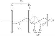
第一极化器可具有第一极化表面,第二极化器可具有不同于第一极化表面的第二极化表面。The first polarizer may have a first polarizing surface, and the second polarizer may have a second polarizing surface different from the first polarizing surface.
根据本发明的总体构思的另一个特点,一种电子装置包括:第一半导体芯片;第二半导体芯片;绝缘的电磁屏蔽结构,介于第一半导体芯片和第二半导体芯片之间。绝缘的电磁屏蔽结构包括具有第一传输轴的第一极化器及具有不同于第一传输轴的第二传输轴的第二极化器。According to another feature of the present general inventive concept, an electronic device includes: a first semiconductor chip; a second semiconductor chip; an insulating electromagnetic shielding structure interposed between the first semiconductor chip and the second semiconductor chip. The insulating electromagnetic shielding structure includes a first polarizer having a first transmission axis and a second polarizer having a second transmission axis different from the first transmission axis.
所述电子装置还可包括封装基底,第一半导体芯片和第二半导体芯片可设置在封装基底上。The electronic device may further include a package substrate on which the first semiconductor chip and the second semiconductor chip may be disposed.
第一半导体芯片和第二半导体芯片可竖直地堆叠在封装基底上。The first semiconductor chip and the second semiconductor chip may be vertically stacked on the package substrate.
第一半导体芯片和第二半导体芯片可在封装基底上沿着水平方向彼此隔开。The first semiconductor chip and the second semiconductor chip may be spaced apart from each other in a horizontal direction on the package substrate.
根据本发明的总体构思的另一个特点,一种电子装置包括具有内部空间的壳体。第一绝缘电磁屏蔽结构设置在壳体的内表面上。处理装置设置在壳体的内部空间中。第二绝缘电磁屏蔽结构设置在处理装置内。第一绝缘电磁屏蔽结构和第二绝缘电磁屏蔽结构中的任意一个包括顺序地堆叠的第一极化器和第二极化器。第一极化器具有第一传输轴,第二极化器具有在平面上与第一极化器的第一传输轴正交的第二传输轴。电子装置还可包括与壳体结合的输入/输入(I/O)装置,I/O装置包括暴露到壳体的外部的显示表面。According to another feature of the present general inventive concept, an electronic device includes a case having an inner space. A first insulating electromagnetic shielding structure is disposed on the inner surface of the housing. The processing device is arranged in the inner space of the housing. A second insulating electromagnetic shielding structure is disposed within the processing device. Any one of the first insulating electromagnetic shielding structure and the second insulating electromagnetic shielding structure includes a first polarizer and a second polarizer stacked sequentially. The first polarizer has a first transmission axis, and the second polarizer has a second transmission axis orthogonal to the first transmission axis of the first polarizer in a plane. The electronic device may further include an input/input (I/O) device combined with the case, the I/O device including a display surface exposed to the outside of the case.
附图说明Description of drawings
通过下面结合附图对示例性实施例进行的描述,本发明的总体构思的这些和/或其他特点和效用将会变得明显且更加易于理解,在附图中:These and/or other features and utilities of the present general inventive concept will become apparent and easier to understand through the following description of exemplary embodiments in conjunction with the accompanying drawings, in which:
图1至图11是示出根据本发明的总体构思的示例性实施例的半导体装置的截面图;1 to 11 are cross-sectional views illustrating a semiconductor device according to an exemplary embodiment of the present general inventive concept;
图12A至图12H是示出根据本发明的总体构思的示例性实施例的电磁屏蔽结构的图;12A to 12H are diagrams illustrating an electromagnetic shielding structure according to an exemplary embodiment of the present general inventive concept;
图13至图19B是示出根据本发明的总体构思的一些示例性实施例的制造半导体装置的方法的图;13 to 19B are diagrams illustrating a method of manufacturing a semiconductor device according to some exemplary embodiments of the present general inventive concept;
图20至图65是示出根据本发明的总体构思的示例性实施例的半导体封装的图;20 to 65 are views illustrating a semiconductor package according to an exemplary embodiment of the present general inventive concept;
图66至图72是示出根据本发明的总体构思的示例性实施例的电子装置的截面图;66 to 72 are cross-sectional views illustrating an electronic device according to an exemplary embodiment of the present general inventive concept;
图73是示出根据本发明的总体构思的示例性实施例的电子系统的图;73 is a diagram illustrating an electronic system according to an exemplary embodiment of the present general inventive concept;
图74是示出根据本发明的总体构思的示例性实施例的电子装置的图。FIG. 74 is a diagram illustrating an electronic device according to an exemplary embodiment of the present general inventive concept.
具体实施方式Detailed ways
现在,将详细说明本发明的总体构思的示例性实施例,其示例在附图中示出,在附图中,相同的标号始终指示相同的元件。下面同时参照附图描述示例性实施例,以解释本发明的总体构思。Now, exemplary embodiments of the present general inventive concept will be described in detail, examples of which are illustrated in the accompanying drawings, in which like reference numerals refer to like elements throughout. The exemplary embodiments are described below in order to explain the present general inventive concept while referring to the figures.
在此参照作为本发明的总体构思的示例性实施例的示意性图解的截面图图解描述本发明的总体构思的示例性实施例。同样地,例如,可以预料到会出现由于制造技术和/或公差导致图解的形状发生变化。因此,本发明的总体构思的示例性实施例不应该被解释为限于在此示出的区域的具体形状,而是包括由于(例如)制造导致的形状的偏差。例如,被示出为矩形的蚀刻区域通常将具有圆滑的或弯曲的特征。因此,在附图中示出的区域本质上是示意性的,它们的形状不意在示出装置的区域的精确形状且不意在限制本发明构思的范围。Exemplary embodiments of the present general inventive concept are described herein with reference to cross-sectional illustrations that are schematic illustrations of exemplary embodiments of the present general inventive concept. Also, for example, variations from the shapes of the illustrations as a result of manufacturing techniques and/or tolerances are contemplated. Thus, example embodiments of the present general inventive concept should not be construed as limited to the particular shapes of regions illustrated herein but are to include deviations in shapes that result, for example, from manufacturing. For example, an etched region illustrated as a rectangle will, typically, have rounded or curved features. Thus, the regions illustrated in the figures are schematic in nature and their shapes are not intended to illustrate the precise shape of a region of a device and are not intended to limit the scope of inventive concepts.
图1是根据本发明的总体构思的至少一个示例性实施例的半导体装置的图。FIG. 1 is a diagram of a semiconductor device according to at least one example embodiment of the present general inventive concept.
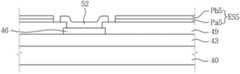
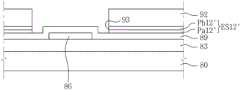
参照图1,可提供半导体基底1。半导体基底1可以是包括半导体集成电路(IC)的硅基底。半导体基底1可具有彼此相对地设置的第一表面FS和第二表面BS。夹层绝缘层3可设置在半导体基底1的其上形成有IC的第一表面FS上。导电焊盘6可设置在夹层绝缘层3上,绝缘层9可设置在具有焊盘6的半导体基底1上。绝缘层可以是钝化层。绝缘层9可具有使焊盘6暴露的开口。下绝缘层12可设置在绝缘层9上。Referring to FIG. 1 , a
金属互连件18可重新分布在下绝缘层12上。重新分布的金属互连件18可通过穿过下绝缘层12形成的通孔16电连接到焊盘6。在至少一个示例性实施例中,金属互连件18包括接触部分19、第一臂部分20及第二臂部分20’。接触部分19延伸穿过通孔16,以接触焊盘6。第一臂部分20从接触部分19的第一端延伸,并可接触绝缘层9和/或下绝缘层12。第二臂部分20’从接触部分19的与第一端相对的第二端延伸,并可接触绝缘层9和/或下绝缘层12。如下面更加详细地描述的,可在第二臂部分20’上形成导电图案。Metal interconnects 18 may be redistributed on lower insulating
焊盘6可以是输入/输出(I/O)焊盘、接地焊盘及电源焊盘中的任意一个。金属互连件18可以是信号线、电源线及接地线中的任意一个。The
上绝缘层24可设置在具有金属互连件18的半导体基底1上。上绝缘层24可具有使金属互连件18的一部分暴露的开口H。金属互连件18的被开口暴露的区域可描述为(例如)重新分布焊盘区域。重新分布焊盘区域可包括第二臂部分20’,第二臂部分20’在开口之下且沿着上绝缘层24延伸,从而通过开口被暴露。An upper insulating
电磁屏蔽结构ES1可设置在上绝缘层24上。电磁屏蔽结构ES1可包括顺序地堆叠的第一极化器Pa1和第二极化器Pb1。第一极化器Pa1可选择性地传输电磁波的第一极化波,而第二极化器Pb1可选择性地传输电磁波的第二极化波。因此,第一极化器Pa1可不传输第二极化波,而第二极化器Pb1可不传输第一极化波。即,可通过第一极化器Pa1和第二极化器Pb1中的任意一个传输电磁波,而可通过第一极化器Pa1和第二极化器Pb1中余下的那一个阻挡电磁波。The electromagnetic shielding structure ES1 may be disposed on the upper insulating
在一些示例性实施例中,电磁屏蔽结构ES1可以是绝缘的电磁屏蔽结构。例如,电磁屏蔽结构ES1可包括由绝缘材料形成的第一极化器Pa1及由绝缘材料形成的第二极化器Pb1。所述绝缘材料可由包括绝缘颗粒的绝缘树脂形成,所述绝缘颗粒包括但不限于硅石、云母、石英、玻璃、硅酸钙、硅酸铝、硅酸锆、氧化铝、二氧化钛、钛酸钡、碳酸钙、硫酸钙、氧化铁、硫酸铝锂、硅酸镁及氧化锆。所述绝缘材料还可包括由聚乙烯醇(polyvinylalcohol,PVA)形成的树脂和/或绝缘膜。In some exemplary embodiments, the electromagnetic shielding structure ES1 may be an insulating electromagnetic shielding structure. For example, the electromagnetic shielding structure ES1 may include a first polarizer Pa1 formed of an insulating material and a second polarizer Pb1 formed of an insulating material. The insulating material may be formed of an insulating resin including insulating particles including, but not limited to, silica, mica, quartz, glass, calcium silicate, aluminum silicate, zirconium silicate, alumina, titanium dioxide, barium titanate, Calcium Carbonate, Calcium Sulfate, Iron Oxide, Lithium Aluminum Sulfate, Magnesium Silicate and Zirconia. The insulating material may further include a resin and/or an insulating film formed of polyvinylalcohol (PVA).
例如,电磁屏蔽结构ES1可包括利用聚乙烯醇(PVA)基膜(例如,PVA、聚乙烯醇缩甲醛(polyvinyl formal,PVF)或者聚乙烯醇缩乙醛(polyvinylacetal,PVA))形成的第一极化器Pa1和第二极化器Pb1。例如,第一极化器Pa1和第二极化器Pb1中的每个可以是碘极化器(iodic polarizer),在碘极化器中,碘分子在聚乙烯醇(PVA)聚合物之间沿着一个方向定向。更具体地说,第一极化器Pa1可以是第一材料层,在第一材料层中,碘分子沿着第一方向被定向在PVA聚合物之间,而第二极化器Pb1可以是第二材料层,在第二材料层中,碘分子沿着与第一方向正交的第二方向被定向在PVA聚合物之间。因此,第一极化器Pa1和第二极化器Pb1可具有彼此正交的传输轴(或者极化轴)。For example, the electromagnetic shielding structure ES1 may include a first polyvinyl alcohol (PVA) base film (for example, PVA, polyvinyl formal (PVF) or polyvinyl acetal (polyvinylacetal, PVA)). polarizer Pa1 and a second polarizer Pb1. For example, each of the first polarizer Pa1 and the second polarizer Pb1 may be an iodic polarizer in which iodine molecules are between polyvinyl alcohol (PVA) polymers Orient in one direction. More specifically, the first polarizer Pa1 may be a first material layer in which iodine molecules are oriented between PVA polymers along a first direction, and the second polarizer Pb1 may be A second material layer in which iodine molecules are oriented between the PVA polymers along a second direction orthogonal to the first direction. Accordingly, the first polarizer Pa1 and the second polarizer Pb1 may have transmission axes (or polarization axes) orthogonal to each other.
根据本发明的总体构思的示例性实施例的极化器不限于碘极化器。例如,虽然上述碘极化器可用于根据本发明的总体构思的半导体芯片、半导体装置、半导体封装、电子装置及电子系统,但是由除了碘材料之外的材料形成的极化器也可用于根据本发明的总体构思的半导体芯片、半导体装置、半导体封装、电子装置及电子系统。The polarizer according to the exemplary embodiment of the present general inventive concept is not limited to the iodine polarizer. For example, although the above-mentioned iodine polarizers can be used in semiconductor chips, semiconductor devices, semiconductor packages, electronic devices, and electronic systems according to the general inventive concept, polarizers formed of materials other than iodine materials can also be used in accordance with A semiconductor chip, a semiconductor device, a semiconductor package, an electronic device, and an electronic system according to the general concept of the present invention.
在其他示例性实施例中,电磁屏蔽结构ES1可以是导电的电磁屏蔽结构。即,电磁屏蔽结构ES1可包括包含导电材料的第一极化器Pa1和第二极化器Pb1。所述导电材料可包括但不限于铁、铁合金、铜、铝、钼、金、银、钨、碳纳米管、镍及导电聚合物。所述导电材料还可包括(例如)电磁性氧化铁、铬等。In other exemplary embodiments, the electromagnetic shielding structure ES1 may be a conductive electromagnetic shielding structure. That is, the electromagnetic shielding structure ES1 may include a first polarizer Pa1 and a second polarizer Pb1 including a conductive material. The conductive material may include, but is not limited to, iron, iron alloys, copper, aluminum, molybdenum, gold, silver, tungsten, carbon nanotubes, nickel, and conductive polymers. The conductive material may also include, for example, electromagnetic iron oxide, chromium, and the like.
第一极化器Pa1可包括第一基体及设置在第一基体上的一个或多个第一导电图案,而第二极化器Pb1可包括第二基体及设置在第二基体上的一个或多个第二导电图案。第一导电图案和第二导电图案中的每个可包括导电材料,例如,铝(Al)、钼(Mo)、金(Au)、铜(Cu)、银(Ag)、钨(W)、碳纳米管、镍(Ni)或者导电聚合物。这里,第一导电图案可以是沿着第一长度方向布置的线,而第二导电图案可以是沿着与第一长度方向正交的第二长度方向布置的线。因此,由于第一导电图案和第二导电图案彼此正交,所以第一极化器Pa1和第二极化器Pb1可具有不同的传输轴。电磁屏蔽结构ES1可具有开口H’。电磁屏蔽结构ES1的开口H’可围绕上绝缘层24的开口H形成,从而使上绝缘层24的开口暴露。The first polarizer Pa1 may include a first base and one or more first conductive patterns disposed on the first base, while the second polarizer Pb1 may include a second base and one or more conductive patterns disposed on the second base. a plurality of second conductive patterns. Each of the first conductive pattern and the second conductive pattern may include a conductive material such as aluminum (Al), molybdenum (Mo), gold (Au), copper (Cu), silver (Ag), tungsten (W), Carbon nanotubes, nickel (Ni), or conductive polymers. Here, the first conductive pattern may be lines arranged along a first length direction, and the second conductive pattern may be lines arranged along a second length direction orthogonal to the first length direction. Accordingly, since the first conductive pattern and the second conductive pattern are orthogonal to each other, the first polarizer Pa1 and the second polarizer Pb1 may have different transmission axes. The electromagnetic shielding structure ES1 may have an opening H'. The opening H' of the electromagnetic shielding structure ES1 may be formed around the opening H of the upper insulating
在一些示例性实施例中,电磁屏蔽结构ES1的开口H’的宽度W2可大于上绝缘层24的开口H的宽度W1。In some exemplary embodiments, the width W2 of the opening H' of the electromagnetic shielding structure ES1 may be greater than the width W1 of the opening H of the upper insulating
导电结构27a可设置在被上绝缘层24暴露的金属互连件18上。例如,导电结构27a可包括焊球。在图1中示出的至少一个示例性实施例中,导电结构27a形成在上绝缘层24上,并延伸到开口H中,以接触金属互连件18的第二臂部分20’。A conductive structure 27 a may be disposed on the
在一些示例性实施例中,电磁屏蔽结构ES1可与导电结构27a隔开。导电结构27a的宽度W3可小于电磁屏蔽结构ES1的开口H’的宽度W2。因此,由于电磁屏蔽结构ES1和导电结构27a彼此隔开,所以电磁屏蔽结构ES1可以是绝缘的电磁屏蔽结构或者导电的电磁屏蔽结构。In some exemplary embodiments, the electromagnetic shielding structure ES1 may be separated from the conductive structure 27a. The width W3 of the conductive structure 27a may be smaller than the width W2 of the opening H' of the electromagnetic shielding structure ES1. Therefore, since the electromagnetic shielding structure ES1 and the conductive structure 27a are separated from each other, the electromagnetic shielding structure ES1 may be an insulating electromagnetic shielding structure or a conductive electromagnetic shielding structure.
现在,将参照图2描述根据本发明的总体构思的其他示例性实施例的半导体装置。Now, semiconductor devices according to other exemplary embodiments of the present general inventive concept will be described with reference to FIG. 2 .
参照图2,如图1中示出的那样,夹层绝缘层3、焊盘6、绝缘层9、下绝缘层12、重新分布金属互连件18及具有开口的上绝缘层24可设置在具有IC的半导体基底1上。Referring to FIG. 2, as shown in FIG. 1, the
电磁屏蔽结构ES2可设置在上绝缘层24上。电磁屏蔽结构ES2可具有与上绝缘层24的开口自对准的开口。The electromagnetic shielding structure ES2 may be disposed on the upper insulating
导电结构27b可设置在上绝缘层24和电磁屏蔽结构ES2上。导电结构27b可穿过上绝缘层24和电磁屏蔽结构ES2的自对准的开口,并覆盖电磁屏蔽结构ES2的一部分。如图1中的那样,电磁屏蔽结构ES2可包括第一极化器Pa2和第二极化器Pb2。The
由于电磁屏蔽结构ES2的一部分由导电结构27b覆盖,所以电磁屏蔽结构ES2可以是绝缘的电磁屏蔽结构。Since a part of the electromagnetic shielding structure ES2 is covered by the
现在,将参照图3描述根据本发明的总体构思的其他示例性实施例的半导体装置。Now, semiconductor devices according to other exemplary embodiments of the present general inventive concept will be described with reference to FIG. 3 .
参照图3,如图1中的那样,夹层绝缘层3、焊盘6、绝缘层9、下绝缘层12、重新分布金属互连件18及上绝缘层24可设置在具有IC的半导体基底1上。如图1中的那样,上绝缘层24可包括使金属互连件18的一部分暴露的开口H。例如,金属互连件18的第二臂部分20’可通过形成在上绝缘层24中的开口H暴露。Referring to FIG. 3, as in FIG. 1, an
电磁屏蔽结构ES3可设置在上绝缘层24上。如图1中的那样,电磁屏蔽结构ES3可包括第一极化器Pa3和第二极化器Pb3。The electromagnetic shielding structure ES3 may be disposed on the upper insulating
如图1中的那样,电磁屏蔽结构ES3可包括开口H’,开口H’的宽度W2’大于上绝缘层24的开口的宽度W1’。导电结构27c可设置在上绝缘层24上。导电结构27c的宽度W3’可大于电磁屏蔽结构ES3的开口H’的宽度W2’,并覆盖电磁屏蔽结构ES3的一部分。因此,电磁屏蔽结构ES3可以是绝缘的电磁屏蔽结构。As in FIG. 1 , the electromagnetic shielding structure ES3 may include an opening H' having a width W2' greater than a width W1' of the opening of the upper insulating
虽然在图1至图3中示出的示例性实施例提供设置在半导体基底1的前表面(即,第一表面FS)上的电磁屏蔽结构ES1、ES2及ES3,但是本发明的总体构思不限于此。例如,如图4所示,本发明的总体构思可提供设置在半导体基底1的后表面(即,第二表面BS)上的电磁屏蔽结构ES4。如图1中的那样,图4的电磁屏蔽结构ES4可包括第一极化器Pa4和第二极化器Pb4。Although the exemplary embodiments shown in FIGS. 1 to 3 provide electromagnetic shielding structures ES1, ES2, and ES3 disposed on the front surface (ie, the first surface FS) of the
现在,将参照图5描述根据本发明的总体构思的其他示例性实施例的半导体装置。Now, semiconductor devices according to other exemplary embodiments of the present general inventive concept will be described with reference to FIG. 5 .
参照图5,如图1中的那样,夹层绝缘层43和焊盘46可设置在半导体基底40上。绝缘层49可设置在具有焊盘46的半导体基底40上。绝缘层49可具有使焊盘46的顶表面部分或完全暴露的开口。绝缘层49可以是钝化层。Referring to FIG. 5 , as in FIG. 1 ,
电磁屏蔽结构ES5可设置在绝缘层49上。如图1中的那样,电磁屏蔽结构ES5可包括第一极化器Pa5和第二极化器Pb5。The electromagnetic shielding structure ES5 may be disposed on the insulating
导电结构52可设置在被绝缘层49的开口暴露的焊盘46上。导电结构52可以是被构造成将半导体装置与另一装置或芯片电连接的I/O焊盘。如图1中的那样,导电结构52可与电磁屏蔽结构ES5隔开。The
现在,将参照图6描述根据本发明的总体构思的其他示例性实施例的半导体装置。Now, semiconductor devices according to other exemplary embodiments of the present general inventive concept will be described with reference to FIG. 6 .
参照图6,如图5中的那样,夹层绝缘层43、焊盘46、具有开口的绝缘层49及导电结构52可设置在半导体基底40上。与图5不同的是,电磁屏蔽结构ES6可设置在绝缘层49上,以覆盖导电结构52的顶表面的一部分。如图2中的那样,电磁屏蔽结构ES6可包括由绝缘材料形成的第一极化器Pa6及由绝缘材料形成的第二极化器Pb6。Referring to FIG. 6 , as in FIG. 5 , an
虽然在图5和图6中示出的示例性实施例提供设置在半导体基底40的前表面(即,第一表面FS)上的电磁屏蔽结构ES5和ES6,但是本发明的总体构思不限于此。例如,如图7所示,本发明的总体构思可提供设置在半导体基底40的后表面(即,第二表面BS)上的电磁屏蔽结构ES7。如图1中的那样,图7的电磁屏蔽结构ES7可包括第一极化器Pa7和第二极化器Pb7。Although the exemplary embodiments shown in FIGS. 5 and 6 provide the electromagnetic shielding structures ES5 and ES6 disposed on the front surface (ie, the first surface FS) of the
本发明的总体构思不仅可包括电磁屏蔽结构仅设置在半导体基底40的前表面FS和后表面BS中的一个上的示例性实施例,而且可包括电磁屏蔽结构设置在半导体基底40的前表面FS和后表面BS中的每个上的示例性实施例。The present general inventive concept may include not only an exemplary embodiment in which the electromagnetic shielding structure is provided on only one of the front surface FS and the back surface BS of the
现在,将参照图8描述根据本发明的总体构思的其他示例性实施例的半导体装置。Now, semiconductor devices according to other exemplary embodiments of the present general inventive concept will be described with reference to FIG. 8 .
参照图8,第一电磁屏蔽结构ES8_1可设置在半导体基底40的前表面FS上,而第二电磁屏蔽结构ES8_2可设置在半导体基底40的后表面BS上。即,电磁屏蔽结构ES8可包括第一电磁屏蔽结构ES8_1和第二电磁屏蔽结构ES8_2。因此,半导体基底40的IC可被电磁屏蔽结构ES8保护而免受外部电磁干扰(EMI)影响。Referring to FIG. 8 , the first electromagnetic shielding structure ES8_1 may be disposed on the front surface FS of the
第一电磁屏蔽结构ES8_1可包括第一极化器Pa8_1和第二极化器Pb8_1,而第二电磁屏蔽结构ES8_2可包括第三极化器Pa8_2和第四极化器Pb8_2。The first electromagnetic shielding structure ES8_1 may include a first polarizer Pa8_1 and a second polarizer Pb8_1, and the second electromagnetic shielding structure ES8_2 may include a third polarizer Pa8_2 and a fourth polarizer Pb8_2.
虽然如图6中的那样,图8示出了第一电磁屏蔽结构ES8_1覆盖导电结构52的一部分,但是本发明的总体构思的示例性实施例不限于此。例如,如图5中的那样,第一电磁屏蔽结构ES8_1可与导电结构52隔开。同时,如图9中的那样,可提供具有被导电结构52’部分地覆盖的顶表面的电磁屏蔽结构ES9。这里,电磁屏蔽结构ES9可包括第一极化器Pa9和第二极化器Pb9。Although FIG. 8 illustrates that the first electromagnetic shielding structure ES8_1 covers a portion of the
现在,将参照图10描述根据本发明的总体构思的其他示例性实施例的半导体装置。Now, semiconductor devices according to other exemplary embodiments of the present general inventive concept will be described with reference to FIG. 10 .
参照图10,夹层绝缘层63可设置在半导体基底60上。焊盘66可设置在夹层绝缘层63上,第一绝缘层69可设置半导体基底60上,以覆盖焊盘66。具有开口的电磁屏蔽结构ES10可设置在第一绝缘层69上。电磁屏蔽结构ES10可包括第一极化器Pa10和第二极化器Pb10。Referring to FIG. 10 , an interlayer insulating layer 63 may be disposed on the semiconductor substrate 60 . The pad 66 may be disposed on the interlayer insulating layer 63 , and the first insulating layer 69 may be disposed on the semiconductor substrate 60 to cover the pad 66 . An electromagnetic shielding structure ES10 having an opening may be disposed on the first insulating layer 69 . The electromagnetic shielding structure ES10 may include a first polarizer Pa10 and a second polarizer Pb10.
第二绝缘层72可设置在电磁屏蔽结构ES10上。开口75可顺序地穿过第二绝缘层72和第一绝缘层69,并使焊盘66暴露。导电结构78可设置在被开口75暴露的焊盘66上。The second insulating layer 72 may be disposed on the electromagnetic shielding structure ES10. The opening 75 may sequentially pass through the second insulating layer 72 and the first insulating layer 69 and expose the pad 66 . A conductive structure 78 may be disposed on the pad 66 exposed by the opening 75 .
穿过第一绝缘层69和第二绝缘层72形成的开口75可穿过电磁屏蔽结构ES10的开口。即,穿过第一绝缘层69和第二绝缘层72形成的开口75的内壁可与电磁屏蔽结构ES10隔开。The opening 75 formed through the first insulating layer 69 and the second insulating layer 72 may pass through the opening of the electromagnetic shielding structure ES10. That is, an inner wall of the opening 75 formed through the first insulating layer 69 and the second insulating layer 72 may be separated from the electromagnetic shielding structure ES10.
电磁屏蔽结构ES10可被第一绝缘层69和第二绝缘层72围绕和绝缘,并与导电结构78隔开。因此,电磁屏蔽结构ES10可以是绝缘的或导电的电磁屏蔽结构。The electromagnetic shielding structure ES10 may be surrounded and insulated by the first insulating layer 69 and the second insulating layer 72 and separated from the conductive structure 78 . Therefore, the electromagnetic shielding structure ES10 may be an insulating or a conductive electromagnetic shielding structure.
现在,将参照图11描述根据本发明的总体构思的其他示例性实施例的半导体装置。Now, semiconductor devices according to other exemplary embodiments of the present general inventive concept will be described with reference to FIG. 11 .
参照图11,如图10中的那样,夹层绝缘层63和焊盘66可设置在半导体基底60上。第一绝缘层69可设置在夹层绝缘层63上,以覆盖焊盘66。电磁屏蔽结构ES11可设置在第一绝缘层69上。电磁屏蔽结构ES11可包括第一极化器Pa11和第二极化器Pb11。Referring to FIG. 11 , as in FIG. 10 , interlayer insulating layers 63 and pads 66 may be disposed on the semiconductor substrate 60 . A first insulating layer 69 may be disposed on the interlayer insulating layer 63 to cover the pad 66 . The electromagnetic shielding structure ES11 may be disposed on the first insulating layer 69 . The electromagnetic shielding structure ES11 may include a first polarizer Pa11 and a second polarizer Pb11.
第二绝缘层72’可设置在电磁屏蔽结构ES11上。开口75’可顺序地穿过第二绝缘层72’、电磁屏蔽结构ES11及第一绝缘层69,并使焊盘66暴露。导电结构78’可形成在被开口75’暴露的焊盘66上。The second insulating layer 72' may be disposed on the electromagnetic shielding structure ES11. The opening 75' can pass through the second insulating layer 72', the electromagnetic shielding structure ES11 and the first insulating layer 69 sequentially, and expose the pad 66. A conductive structure 78' may be formed on the pad 66 exposed by the opening 75'.
电磁屏蔽结构ES11的一部分可被开口75’暴露,并与导电结构78’接触。在图11中示出的至少一个示例性实施例中,第一极化器Pa11和第二极化器Pb11中的每个接触导电结构78’。电磁屏蔽结构ES11可以是绝缘的电磁屏蔽结构。A portion of the electromagnetic shielding structure ES11 may be exposed by the opening 75' and be in contact with the conductive structure 78'. In at least one exemplary embodiment shown in FIG. 11 , each of the first polarizer Pa11 and the second polarizer Pb11 contacts the conductive structure 78'. The electromagnetic shielding structure ES11 may be an insulating electromagnetic shielding structure.
如在参照图1至图11描述的本发明的总体构思的示例性实施例中的那样,电磁屏蔽结构可以以各种形状设置在半导体基底的前表面和/或后表面上。电磁屏蔽结构可防止由形成在半导体基底上的IC产生的电磁波发射到外部,并保护形成在半导体基底上的IC和互连结构而免受由外部半导体芯片或电子装置产生的电磁波影响。As in the exemplary embodiments of the present general inventive concept described with reference to FIGS. 1 to 11 , the electromagnetic shielding structure may be disposed in various shapes on the front and/or rear surface of the semiconductor substrate. The electromagnetic shielding structure prevents electromagnetic waves generated from ICs formed on the semiconductor substrate from being emitted to the outside, and protects the ICs and interconnection structures formed on the semiconductor substrate from electromagnetic waves generated from external semiconductor chips or electronic devices.
现在,将参照图12A至图12H描述根据本发明的总体构思的示例性实施例的电磁屏蔽结构。Now, an electromagnetic shielding structure according to an exemplary embodiment of the present general inventive concept will be described with reference to FIGS. 12A to 12H .
根据本发明的总体构思的示例性实施例,非极化的电磁波可在到达电磁屏蔽结构的第二极化器之前先到达电磁屏蔽结构的第一极化器,或者在到达电磁屏蔽结构的第一极化器之前先到达电磁屏蔽结构的第二极化器。According to an exemplary embodiment of the present general inventive concept, non-polarized electromagnetic waves may first reach the first polarizer of the electromagnetic shielding structure before reaching the second polarizer of the electromagnetic shielding structure, or may arrive at the first polarizer of the electromagnetic shielding structure. The first polarizer is preceded by a second polarizer of the electromagnetic shielding structure.
现在,将参照图12A描述这样的示例性实施例:当非极化电磁波在到达电磁屏蔽结构的第二极化器之前先到达电磁屏蔽结构的第一极化器时,电磁屏蔽结构会阻挡电磁波。Now, an exemplary embodiment will be described with reference to FIG. 12A in which an electromagnetic shielding structure blocks electromagnetic waves when a non-polarized electromagnetic wave first reaches the first polarizer of the electromagnetic shielding structure before reaching the second polarizer of the electromagnetic shielding structure. .
参照图12A,可提供包括第一极化器Pa和第二极化器Pb的电磁屏蔽结构ES。电磁波EW可从电磁屏蔽结构ES的外部朝着电磁屏蔽结构ES行进,并且与第二极化器Pb相比更早地到达第一极化器Pa。Referring to FIG. 12A , an electromagnetic shielding structure ES including a first polarizer Pa and a second polarizer Pb may be provided. The electromagnetic wave EW may travel toward the electromagnetic shielding structure ES from the outside of the electromagnetic shielding structure ES, and reach the first polarizer Pa earlier than the second polarizer Pb.
电磁波EW可包括第一极化波Pv及不同于第一极化波Pv的第二极化波Ph。例如,第一极化波Pv可以是竖直波,而第二极化波Ph可以是水平波。这里,为了清楚起见,假设电磁波EW包括第一极化波Pv和第二极化波Ph。然而,应该理解的是,电磁波EW实际上处于非极化状态。The electromagnetic wave EW may include a first polarized wave Pv and a second polarized wave Ph different from the first polarized wave Pv. For example, the first polarized wave Pv may be a vertical wave, and the second polarized wave Ph may be a horizontal wave. Here, for the sake of clarity, it is assumed that the electromagnetic wave EW includes the first polarized wave Pv and the second polarized wave Ph. However, it should be understood that the electromagnetic wave EW is actually in a non-polarized state.
第一极化器Pa可选择性地传输电磁波EW的第一极化波Pv,而第二极化器Pb可选择性地传输电磁波EW的第二极化波Ph。因此,非极化波EW可通过第一极化器Pa被极化。即,穿过第一极化器Pa的电磁波可以是第一极化波Pv’。The first polarizer Pa can selectively transmit the first polarized wave Pv of the electromagnetic wave EW, and the second polarizer Pb can selectively transmit the second polarized wave Ph of the electromagnetic wave EW. Therefore, the unpolarized wave EW can be polarized by the first polarizer Pa. That is, the electromagnetic wave passing through the first polarizer Pa may be the first polarized wave Pv'.
穿过第一极化器Pa的第一极化波Pv’基本上不可能穿过第二极化器Pb。具体地说,由于第二极化器Pb选择性地传输与第一极化波Pv不同的第二极化波Ph,所以穿过第一极化器Pa的第一极化波Pv’不可能穿过第二极化器Pb。It is substantially impossible for the first polarized wave Pv' passing through the first polarizer Pa to pass through the second polarizer Pb. Specifically, since the second polarizer Pb selectively transmits the second polarized wave Ph different from the first polarized wave Pv, it is impossible for the first polarized wave Pv' to pass through the first polarizer Pa through the second polarizer Pb.
即使第一极化波Pv’的一部分穿过第二极化器Pb,穿过第二极化器Pb的第一极化波Pv’的强度可减小,并且不可能对人体或电子装置产生有意义的影响。因此,在示例性实施例中,假设忽略第一极化波Pv’的穿过第二极化器Pb的部分。Even if a part of the first polarized wave Pv' passes through the second polarizer Pb, the intensity of the first polarized wave Pv' passing through the second polarizer Pb can be reduced, and it is impossible to cause harm to the human body or electronic devices. meaningful impact. Therefore, in the exemplary embodiment, it is assumed that a portion of the first polarized wave Pv' passing through the second polarizer Pb is ignored.
电磁波EW可被极化,并且仅穿过第一极化器Pa和第二极化器Pb中的一个,但是电磁波EW不可能穿过包括两个不同的极化器Pa和Pb的电磁屏蔽结构ES。因此,包括第一极化器Pa和第二极化器Pb的电磁屏蔽结构ES可阻挡电磁波EW。The electromagnetic wave EW can be polarized and passes through only one of the first polarizer Pa and the second polarizer Pb, but it is impossible for the electromagnetic wave EW to pass through the electromagnetic shielding structure including two different polarizers Pa and Pb ES. Therefore, the electromagnetic shielding structure ES including the first polarizer Pa and the second polarizer Pb can block the electromagnetic wave EW.
现在,将参照图12B描述这样的示例性实施例:当非极化电磁波在到达电磁屏蔽结构ES的第一极化器Pa之前先到达电磁屏蔽结构ES的第二极化器Pb时,电磁屏蔽结构ES阻挡电磁波EW。Now, an exemplary embodiment will be described with reference to FIG. 12B : when a non-polarized electromagnetic wave first reaches the second polarizer Pb of the electromagnetic shielding structure ES before reaching the first polarizer Pa of the electromagnetic shielding structure ES, the electromagnetic shielding The structure ES blocks the electromagnetic wave EW.
参照图12B,如图12A中的那样,可设置包括第一极化器Pa和第二极化器Pb的电磁屏蔽结构ES。Referring to FIG. 12B , as in FIG. 12A , an electromagnetic shielding structure ES including a first polarizer Pa and a second polarizer Pb may be provided.
与图12A不同的是,电磁波EW’可从电磁屏蔽结构ES的外部朝着电磁屏蔽结构ES的第二极化器Pb行进,并在到达第一极化器Pa之前先到达第二极化器Pb。Different from FIG. 12A, the electromagnetic wave EW' can travel from the outside of the electromagnetic shielding structure ES toward the second polarizer Pb of the electromagnetic shielding structure ES, and reach the second polarizer before reaching the first polarizer Pa. Pb.
如参照图12A描述的那样,电磁波EW’可包括第一极化波Pv及不同于第一极化波Pv的第二极化波Ph。因此,非极化电磁波EW’可通过第二极化器Pb被极化。即,穿过第二极化器Pb的电磁波可以是第二极化波Ph’。穿过第二极化器Pb的第二极化波Ph’基本上不可能穿过第一极化器Pa。具体地说,由于第一极化器Pa选择性地传输与第二极化波Ph不同的第一极化波Pv,所以穿过第二极化器Pb的第二极化波Ph’不可能穿过第一极化器Pa。As described with reference to FIG. 12A , the electromagnetic wave EW' may include a first polarized wave Pv and a second polarized wave Ph different from the first polarized wave Pv. Therefore, the non-polarized electromagnetic wave EW' can be polarized by the second polarizer Pb. That is, the electromagnetic wave passing through the second polarizer Pb may be the second polarized wave Ph'. It is substantially impossible for the second polarized wave Ph' passing through the second polarizer Pb to pass through the first polarizer Pa. Specifically, since the first polarizer Pa selectively transmits the first polarized wave Pv different from the second polarized wave Ph, it is impossible for the second polarized wave Ph' to pass through the second polarizer Pb through the first polarizer Pa.
因此,电磁波EW’可被电磁屏蔽结构ES阻挡。Therefore, the electromagnetic wave EW' can be blocked by the electromagnetic shielding structure ES.
现在,将参照图12C描述根据本发明的总体构思的示例性实施例的电磁屏蔽结构。Now, an electromagnetic shielding structure according to an exemplary embodiment of the present general inventive concept will be described with reference to FIG. 12C .
参照图12C,电磁屏蔽结构ES’可包括第一极化器Pa’和第二极化器Pb’。第一极化器Pa’可具有第一极化平面PP1,而第二极化器Pb’可具有与第一极化平面PP1不同的第二极化平面PP2。Referring to FIG. 12C , the electromagnetic shielding structure ES' may include a first polarizer Pa' and a second polarizer Pb'. The first polarizer Pa' may have a first polarization plane PP1, and the second polarizer Pb' may have a second polarization plane PP2 different from the first polarization plane PP1.
第一极化器Pa’可具有第一传输轴ny,而第二极化器Pb’可具有与第一传输轴ny不同方向的第二传输轴nx。此外,第二传输轴nx可处于与第一传输轴ny相交的方向。例如,第二传输轴nx可与第一传输轴ny正交。这里,术语“传输轴”可被解读为极化屏蔽轴。轴的方向可影响极化器的阻挡电磁波的Pa’/Pb’能力的效用。例如,第一极化器的第一轴可抑制电磁波的第一波成分,而处于与第一轴不同方向的第二轴可抑制电磁波的与第一波成分不同的第二波成分。The first polarizer Pa' may have a first transmission axis ny, and the second polarizer Pb' may have a second transmission axis nx in a different direction from the first transmission axis ny. Also, the second transmission axis nx may be in a direction intersecting the first transmission axis ny. For example, the second transmission axis nx may be orthogonal to the first transmission axis ny. Here, the term "transmission axis" can be read as the polarization shielding axis. The orientation of the axis can affect the effectiveness of the Pa'/Pb' ability of the polarizer to block electromagnetic waves. For example, a first axis of a first polarizer can suppress a first wave component of electromagnetic waves, and a second axis in a different direction than the first axis can suppress a second wave component of electromagnetic waves different from the first wave component.
如在上面参照图1描述的那样,当第一极化器Pa’和第二极化器Pb’中的每个是碘极化器(在碘极化器中,碘分子沿着一个方向被定向在PVA聚合物之间)时,传输轴的方向可取决于碘分子排列的方向。因此,第一极化器Pa’和第二极化器Pb’可以是具有彼此正交的传输轴的绝缘极化器。As described above with reference to FIG. 1, when each of the first polarizer Pa' and the second polarizer Pb' is an iodine polarizer (in an iodine polarizer, iodine molecules are Oriented between PVA polymers), the direction of the transport axis can depend on the direction in which the iodine molecules are aligned. Accordingly, the first polarizer Pa' and the second polarizer Pb' may be insulated polarizers having transmission axes orthogonal to each other.
现在,将参照图12D描述根据本发明的总体构思的示例性实施例的电磁屏蔽结构。Now, an electromagnetic shielding structure according to an exemplary embodiment of the present general inventive concept will be described with reference to FIG. 12D .
参照图12D,电磁屏蔽结构ES”可包括第一极化器Pa”和第二极化器Pb”。Referring to FIG. 12D , the electromagnetic shielding structure ES'' may include a first polarizer Pa'' and a second polarizer Pb''.
在一些示例性实施例中,第一极化器Pa”和第二极化器Pb”中的每个可呈膜的形式。在这种情况下,第一极化器Pa”和第二极化器Pb”可通过中间层AI附着到彼此,并构成电磁屏蔽结构ES”。中间层AI可使第一极化器Pa”和第二极化器Pb”附着到彼此。例如,中间层AI可包括被构造成附着第一极化器Pa”和第二极化器Pb”的粘性层。In some exemplary embodiments, each of the first polarizer Pa" and the second polarizer Pb" may be in the form of a film. In this case, the first polarizer Pa" and the second polarizer Pb" can be attached to each other through the intermediate layer AI, and constitute the electromagnetic shielding structure ES". The intermediate layer AI can make the first polarizer Pa" and the second polarizer Pb" are attached to each other. For example, the intermediate layer AI may include an adhesive layer configured to attach the first polarizer Pa" and the second polarizer Pb".
电磁屏蔽结构ES”可设置在保护结构CP上,保护结构CP被构造成保护电磁屏蔽结构ES”而免受电磁波影响。缓冲层AD可设置在保护结构CP和电磁屏蔽结构ES”之间。例如,电磁屏蔽结构ES”可通过缓冲层AD附着到保护结构CP。The electromagnetic shielding structure ES" may be disposed on the protective structure CP configured to protect the electromagnetic shielding structure ES" from electromagnetic waves. The buffer layer AD may be disposed between the protection structure CP and the electromagnetic shielding structure ES". For example, the electromagnetic shielding structure ES" may be attached to the protection structure CP through the buffer layer AD.
现在,将参照图12E描述根据本发明的总体构思的其他示例性实施例的电磁屏蔽结构。Now, electromagnetic shielding structures according to other exemplary embodiments of the present general inventive concept will be described with reference to FIG. 12E .
参照图12E,电磁屏蔽结构ES_1可包括第一焊盘PP1_1和第二焊盘PP2_1。第一焊盘PP1_1可包括第一极化器Pa_1,第二焊盘PP2_1可包括第二极化器Pb_1。Referring to FIG. 12E , the electromagnetic shielding structure ES_1 may include a first pad PP1_1 and a second pad PP2_1 . The first pad PP1_1 may include a first polarizer Pa_1, and the second pad PP2_1 may include a second polarizer Pb_1.
更具体地说,第一极化器Pa_1可包括设置在第一焊盘PP1_1的第一基体BA1上的多个第一极化元件PE1。所述多个第一极化元件PF1可根据第一图案PT1布置。第一图案PT1可包括使所述多个第一极化元件PE1布置为彼此隔开的线图案。此外,每个第一极化元件PF1可沿着第一方向沿着第一焊盘PP1_1的第一基体BA1延伸,所述第一方向可提供第一极化器Pa_1的第一传输轴。More specifically, the first polarizer Pa_1 may include a plurality of first polarization elements PE1 disposed on the first base BA1 of the first pad PP1_1 . The plurality of first polarization elements PF1 may be arranged according to a first pattern PT1. The first pattern PT1 may include a line pattern in which the plurality of first polarization elements PE1 are arranged to be spaced apart from each other. In addition, each first polarization element PF1 may extend along the first base BA1 of the first pad PP1_1 along a first direction, which may provide a first transmission axis of the first polarizer Pa_1 .
第一极化元件PF1可以是导电元件。例如,第一极化元件PF1可包括导电材料,例如,Al、Mo、Au、Cu、Ag、W、碳纳米管、Ni或导电聚合物。The first polarizing element PF1 may be a conductive element. For example, the first polarization element PF1 may include a conductive material such as Al, Mo, Au, Cu, Ag, W, carbon nanotubes, Ni, or a conductive polymer.
第二极化器Pb_1可包括设置在第二焊盘PP2_1的第二基体BA2上的多个第二极化元件PE2。所述多个第二极化元件PE2可根据第二图案PT2布置。第二图案PT2使所述多个第二极化元件PE2彼此隔开。此外,每个第二极化元件PE2可沿着与第一极化元件PE1的第一方向不同的第二方向沿着第二焊盘PP2_1的第一基体BA2延伸。因此,第二极化元件PE2的第二方向可提供与第一极化器Pa_1的第一传输轴不同的第二极化器Pb_1的第二传输轴。在至少一个示例性实施例中,第二极化元件PE2的第二方向与第一极化元件PE1的第一方向正交。因此,第二极化器Pb_1的第二传输轴可与第一极化器Pa_1的第一传输轴正交。The second polarizer Pb_1 may include a plurality of second polarization elements PE2 disposed on the second base BA2 of the second pad PP2_1 . The plurality of second polarization elements PE2 may be arranged according to a second pattern PT2. The second pattern PT2 separates the plurality of second polarization elements PE2 from each other. In addition, each second polarization element PE2 may extend along the first base BA2 of the second pad PP2_1 along a second direction different from the first direction of the first polarization element PE1. Therefore, the second orientation of the second polarizing element PE2 may provide a second transmission axis of the second polarizer Pb_1 that is different from the first transmission axis of the first polarizer Pa_1 . In at least one exemplary embodiment, the second direction of the second polarization element PE2 is orthogonal to the first direction of the first polarization element PE1. Therefore, the second transmission axis of the second polarizer Pb_1 may be orthogonal to the first transmission axis of the first polarizer Pa_1.
第二极化元件PE2可以是导电元件。例如,第二极化元件PE2可包括导电材料,例如,Al、Mo、Au、铂(Pt)、Cu、Ag、W、碳纳米管、Ni或导电聚合物。The second polarization element PE2 may be a conductive element. For example, the second polarization element PE2 may include a conductive material such as Al, Mo, Au, platinum (Pt), Cu, Ag, W, carbon nanotubes, Ni, or a conductive polymer.
第一基体BA1和第二基体BA2中的每个可以是由树脂形成的膜,或者是由被保护而免受电磁波影响的电磁保护对象的一部分(例如,诸如氧化硅层、氮化硅层或者聚酰亚胺层的材料层)。第一图案PT1的长度方向可以是第一方向Dy,而第二图案PT2的长度方向可以是与第一方向Dy正交的第二方向Dx。因此,从俯视图上看,第一图案PT1可与第二图案PT2正交。Each of the first base BA1 and the second base BA2 may be a film formed of a resin, or a part of an electromagnetic protection object (for example, such as a silicon oxide layer, a silicon nitride layer, or material layer of polyimide layer). A length direction of the first pattern PT1 may be a first direction Dy, and a length direction of the second pattern PT2 may be a second direction Dx orthogonal to the first direction Dy. Therefore, from a top view, the first pattern PT1 may be orthogonal to the second pattern PT2.
在其他示例性实施例中,第一图案PT1和第二图案PT2中的每个可以是包括金属颗粒的绝缘图案。即,在至少一个示例性实施例中,所述多个极化元件PE1/PE2可包括金属颗粒,同时仍然提供绝缘效果。In other exemplary embodiments, each of the first pattern PT1 and the second pattern PT2 may be an insulating pattern including metal particles. That is, in at least one example embodiment, the plurality of polarization elements PE1/PE2 may include metal particles while still providing an insulating effect.
现在,将参照图12F描述在本发明的总体构思的至少一个示例性实施例中的在图12E中示出的电磁屏蔽结构。应用的示例性实施例应该被解读为本发明的总体构思的实施例的示例,因此,本发明的总体构思不限于此。Now, the electromagnetic shielding structure shown in FIG. 12E in at least one exemplary embodiment of the present general inventive concept will be described with reference to FIG. 12F . The applied exemplary embodiments should be construed as examples of embodiments of the present general inventive concept, and thus, the present general inventive concept is not limited thereto.
参照图12F,如参照图12E描述的那样,电磁屏蔽结构ES_1a可包括顺序地堆叠的第一极化器Pa_1a和第二极化器Pb_1a。此外,第一极化器Pa_1a可包括设置在第一基体BA1’上的第一图案PT1’,而第二极化器Pb_1a可包括设置在第二基体BA2’上的第二图案PT2’。第一图案PT1’可与第二图案PT2’隔开。Referring to FIG. 12F , as described with reference to FIG. 12E , the electromagnetic shielding structure ES_1a may include the first and second polarizers Pa_1a and Pb_1a that are sequentially stacked. In addition, the first polarizer Pa_1a may include a first pattern PT1' disposed on the first base BA1', and the second polarizer Pb_1a may include a second pattern PT2' disposed on the second base BA2'. The first pattern PT1' may be spaced apart from the second pattern PT2'.
第一覆盖层Ca可设置在第一基体BA1’上,以覆盖第一图案PT1’。第一覆盖层Ca可由绝缘材料形成。第二覆盖层Cb可设置在第二基体BA2’上,以覆盖第二图案PT2’。The first capping layer Ca may be disposed on the first base BA1' to cover the first patterns PT1'. The first capping layer Ca may be formed of an insulating material. The second covering layer Cb may be disposed on the second base BA2' to cover the second patterns PT2'.
由于第一极化器Pa_1a和第二极化器Pb_1a可顺序地堆叠,所以第二基体BA2’可设置在第一覆盖层Ca上。Since the first polarizer Pa_1a and the second polarizer Pb_1a may be sequentially stacked, the second base BA2' may be disposed on the first capping layer Ca.
在一些示例性实施例中,第一基体BA1’可以是被保护而免受电磁波影响的保护结构的部分区域。例如,第一基体BA1’可以是半导体晶圆的顶部区域或底部区域的一部分。例如,绝缘层可形成在包括IC和互连线的半导体晶圆上,并用作在示例性实施例中描述的第一基体BA1’。多个第一图案PT1’可利用半导体工艺形成在绝缘层(即,第一基体BA1’)上,且彼此隔开。In some exemplary embodiments, the first base BA1' may be a partial region of a protection structure that is protected from electromagnetic waves. For example, the first base body BA1' may be part of the top region or the bottom region of the semiconductor wafer. For example, an insulating layer may be formed on a semiconductor wafer including ICs and interconnection lines, and used as the first base BA1' described in the exemplary embodiment. A plurality of first patterns PT1' may be formed on the insulating layer (i.e., the first base BA1') using a semiconductor process and spaced apart from each other.
在另一种情况下,多个导线可彼此隔开地布置在具有绝缘特性的膜形式的第一基体BA1’上,并用作极化器。因此,根据本发明的总体构思的电磁屏蔽结构ES_1a可利用各种方法形成。In another case, a plurality of wires may be arranged spaced apart from each other on the first base BA1' in the form of a film having insulating properties, and used as a polarizer. Accordingly, the electromagnetic shielding structure ES_1a according to the present general inventive concept may be formed using various methods.
现在,将参照图12G描述本发明的总体构思的另一示例性实施例的图12E的电磁屏蔽结构。Now, the electromagnetic shielding structure of FIG. 12E , which is another exemplary embodiment of the present general inventive concept, will be described with reference to FIG. 12G .
参照图12G,如图12F中的那样,可提供包括顺序地堆叠的第一极化器Pa_1b和第二极化器Pb_1b的电磁屏蔽结构ES_1b。第一极化器Pa_1b可包括第一基体BA1”及设置在第一基体BA1”上的第一图案PT1”。第二极化器Pb_1b可包括可覆盖第一图案PT1”的第二基体BA2”及第二图案PT2”。覆盖层C可设置在第二基体BA2”上,以覆盖第二图案PT2”。Referring to FIG. 12G , as in FIG. 12F , an electromagnetic shielding structure ES_1b including a first polarizer Pa_1b and a second polarizer Pb_1b sequentially stacked may be provided. The first polarizer Pa_1b may include a first base BA1" and a first pattern PT1" disposed on the first base BA1". The second polarizer Pb_1b may include a second base BA2" that may cover the first pattern PT1". and the second pattern PT2". The cover layer C may be disposed on the second base BA2" to cover the second pattern PT2".
第二基体BA2”可被设置为覆盖第一极化器Pa_1b的第一图案PT1”,并减小第一极化器Pa_1b和第二极化器Pb_1b的整个厚度。因此,具有减小的厚度的电磁屏蔽结构ES_1b可容易地应用于要求厚度小的便携式电子装置。The second base BA2 ″ may be disposed to cover the first pattern PT1 ″ of the first polarizer Pa_1b and reduce the overall thickness of the first polarizer Pa_1b and the second polarizer Pb_1b. Therefore, the electromagnetic shielding structure ES_1b having a reduced thickness can be easily applied to portable electronic devices requiring a small thickness.
同时,如图12H所示,根据本发明的总体构思的一些示例性实施例的电磁屏蔽结构ES_2可具有穿过电磁屏蔽结构ES_2的一部分形成的一个或多个开口H。这里,电磁屏蔽结构ES_2可包括如上所述的第一极化器Pa和第二极化器Pb。所述一个或多个开口H可用作电连接结构的连接路径,该连接结构被构造成将电信号传输到被屏蔽而免受电磁波影响的保护结构。Meanwhile, as shown in FIG. 12H , the electromagnetic shielding structure ES_2 according to some exemplary embodiments of the present general inventive concept may have one or more openings H formed through a portion of the electromagnetic shielding structure ES_2 . Here, the electromagnetic shielding structure ES_2 may include the first polarizer Pa and the second polarizer Pb as described above. The one or more openings H may serve as a connection path for an electrical connection structure configured to transmit electrical signals to a protective structure that is shielded from electromagnetic waves.
如参照图1至图11所描述的,可提供根据本发明的总体构思的示例性实施例的一些半导体装置。这里,每个半导体装置可包括参照图12A至图12H描述的电磁屏蔽结构中的一个。As described with reference to FIGS. 1 to 11 , some semiconductor devices according to exemplary embodiments of the present general inventive concept may be provided. Here, each semiconductor device may include one of the electromagnetic shielding structures described with reference to FIGS. 12A to 12H .
在下文中,将简要地描述制造具有电磁屏蔽结构的半导体装置的方法。Hereinafter, a method of manufacturing a semiconductor device having an electromagnetic shielding structure will be briefly described.
已经在上面参照图1至图9描述了这样的一些示例性实施例:电磁屏蔽结构设置在半导体基底的前表面和/或后表面上。Some exemplary embodiments in which the electromagnetic shielding structure is disposed on the front surface and/or the rear surface of the semiconductor substrate have been described above with reference to FIGS. 1 to 9 .
在下文中,将参照图13至图17描述根据本发明的总体构思的示例性实施例的制造半导体装置的方法。这里,提出的制造方法仅仅是示例,并不意在具体地限制制造采用电磁屏蔽结构的半导体装置的方法。Hereinafter, a method of manufacturing a semiconductor device according to an exemplary embodiment of the present general inventive concept will be described with reference to FIGS. 13 to 17 . Here, the proposed manufacturing method is only an example, and is not intended to specifically limit the method of manufacturing a semiconductor device employing an electromagnetic shielding structure.
首先,如图13所示,可制备晶圆WF。晶圆WF可以是半导体晶圆。晶圆WF可包括通过划线通道区域SR而彼此隔开的多个芯片区域CR。此外,晶圆WF的边缘的一部分可以是虚拟区域DR。划线通道区域SR可以是被构造成使所述多个芯片区域CR彼此分离的切割区域。First, as shown in FIG. 13, a wafer WF may be prepared. Wafer WF may be a semiconductor wafer. The wafer WF may include a plurality of chip regions CR separated from each other by the scribe channel region SR. Also, a part of the edge of the wafer WF may be a dummy region DR. The scribe lane region SR may be a cutting region configured to separate the plurality of chip regions CR from each other.
现在,将参照图13和图14描述根据本发明的总体构思的示例性实施例的制造半导体装置的方法。Now, a method of manufacturing a semiconductor device according to an exemplary embodiment of the present general inventive concept will be described with reference to FIGS. 13 and 14 .
参照图13和图14,可在晶圆WF的前表面上形成电磁屏蔽结构(操作S1)。这里,如参照图1描述的那样,术语“晶圆的前表面”可指的是半导体晶圆的形成有IC的表面,IC包括诸如晶体管的分立元件及被构造成电连接所述分立元件的金属互连结构。即,术语“晶圆的前表面”可以是图1的半导体基底1的前表面FS。Referring to FIGS. 13 and 14 , an electromagnetic shielding structure may be formed on the front surface of the wafer WF (operation S1 ). Here, as described with reference to FIG. 1 , the term “front surface of the wafer” may refer to a surface of a semiconductor wafer on which ICs including discrete elements such as transistors and devices configured to electrically connect the discrete elements are formed. metal interconnect structure. That is, the term "front surface of the wafer" may be the front surface FS of the
之后,可通过沿着晶圆WF的划线通道区域SR切割晶圆WF使多个芯片彼此分离(操作S3)。因此,每个分离的芯片可用于形成图1中示出的半导体芯片或半导体装置。After that, the plurality of chips may be separated from each other by dicing the wafer WF along the scribe lane region SR of the wafer WF (operation S3 ). Accordingly, each separate chip can be used to form the semiconductor chip or semiconductor device shown in FIG. 1 .
现在,将参照图13和图15描述根据本发明的总体构思的其他示例性实施例的制造半导体装置的方法。Now, a method of manufacturing a semiconductor device according to other exemplary embodiments of the present general inventive concept will be described with reference to FIGS. 13 and 15 .
参照图13和图15,可通过沿着晶圆WF的划线通道区域SR切割晶圆WF使多个芯片CH彼此分离(操作S10)。之后,可在每个分离的芯片的前表面上形成电磁屏蔽结构(操作S13)。Referring to FIGS. 13 and 15 , a plurality of chips CH may be separated from each other by dicing the wafer WF along the scribe lane region SR of the wafer WF (operation S10 ). Thereafter, an electromagnetic shielding structure may be formed on the front surface of each separated chip (operation S13).
现在,将参照图13和图16描述根据本发明的总体构思的其他示例性实施例的制造半导体装置的方法。Now, a method of manufacturing a semiconductor device according to other exemplary embodiments of the present general inventive concept will be described with reference to FIGS. 13 and 16 .
参照图13和图16,可在晶圆WF上执行背面研磨(back grinding)工艺(操作S20)。可在晶圆WF的后表面上执行研磨工艺,从而减小晶圆WF的整个厚度。这里,术语“晶圆的后表面”可指的是晶圆的被设置为与晶圆的上述前表面相对的表面。13 and 16, a back grinding (back grinding) process may be performed on the wafer WF (operation S20). A grinding process may be performed on the rear surface of the wafer WF, thereby reducing the overall thickness of the wafer WF. Here, the term "rear surface of the wafer" may refer to a surface of the wafer disposed opposite to the aforementioned front surface of the wafer.
之后,可在厚度减小的晶圆WF的后表面上形成电磁屏蔽结构(操作S23)。可沿着晶圆WF的划线通道区域SR切割晶圆WF,以使多个芯片彼此分离(操作S26)。因此,分离的芯片可形成图4中示出的半导体芯片或半导体装置。After that, an electromagnetic shielding structure may be formed on the rear surface of the reduced-thickness wafer WF (operation S23). The wafer WF may be diced along the scribe lane region SR of the wafer WF to separate a plurality of chips from each other (operation S26 ). Accordingly, the separated chips can form the semiconductor chip or semiconductor device shown in FIG. 4 .
现在,将参照图13和图17描述根据本发明的总体构思的其他示例性实施例的制造半导体装置的方法。Now, a method of manufacturing a semiconductor device according to other exemplary embodiments of the present general inventive concept will be described with reference to FIGS. 13 and 17 .
参照图13和图17,可通过沿着晶圆WF的划线通道区域SR切割晶圆WF,使多个芯片彼此分离(操作S30),可在每个分离的芯片的后表面上形成电磁屏蔽结构(操作S33)。Referring to FIGS. 13 and 17, a plurality of chips may be separated from each other by dicing the wafer WF along the scribe lane region SR of the wafer WF (operation S30), and electromagnetic shielding may be formed on the rear surface of each separated chip. structure (operation S33).
在其他示例性实施例中,电磁屏蔽结构可形成在分离的芯片的前表面和后表面中的每个上。In other exemplary embodiments, an electromagnetic shielding structure may be formed on each of the front and rear surfaces of separate chips.
在上面参照图10和图11描述了这样的一些示例性实施例:电磁屏蔽结构设置在半导体装置或半导体芯片内。现在,将参照图18A至图19B描述制造在图10和图11中示出的半导体装置的方法的示例。Some exemplary embodiments in which the electromagnetic shielding structure is provided within a semiconductor device or a semiconductor chip are described above with reference to FIGS. 10 and 11 . Now, an example of a method of manufacturing the semiconductor device shown in FIGS. 10 and 11 will be described with reference to FIGS. 18A to 19B .
现在,首先将参照图18A至图18D描述根据本发明的总体构思的其他示例性实施例的制造半导体装置的方法。Now, a method of manufacturing a semiconductor device according to other exemplary embodiments of the present general inventive concept will first be described with reference to FIGS. 18A to 18D .
参照图18A,夹层绝缘层83可形成在半导体基底80上。导电图案86可形成在夹层绝缘层83上。导电图案86可以是半导体装置的焊盘或互连件。第一绝缘层89可形成在具有导电图案86的半导体基底80上。第一绝缘层89可由诸如氧化硅或氮化硅的绝缘材料形成。Referring to FIG. 18A , an
第一极化器Pa12和第二极化器Pb12可顺序地堆叠在第一绝缘层89上。The first polarizer Pa12 and the second polarizer Pb12 may be sequentially stacked on the first insulating
具有开口的掩模92可形成在第二极化器Pb12上。掩膜92可以是光刻胶图案。A
参照图18B,第一极化器Pa12’和第二极化器Pb12’可利用掩膜92作为蚀刻掩模被蚀刻,从而形成第一开口93。因此,具有第一极化器Pa12’和第二极化器Pb12’的电磁屏蔽结构ES12’可具有第一开口93。Referring to FIG. 18B , the first polarizer Pa12' and the second polarizer Pb12' may be etched using the
之后,可去除掩模92。Afterwards,
参照图18C,第二绝缘层95可形成在具有电磁屏蔽结构ES12’的半导体基底80上。第二绝缘层95可由诸如聚酰亚胺、氮化硅或者氧化硅的绝缘材料形成。Referring to FIG. 18C, a second insulating
参照图18D,第二开口97可形成为顺序地穿过第二绝缘层95和第一绝缘层89,并使导电图案86暴露。电磁屏蔽结构ES12’的第一开口93的宽度L1可大于第二开口97的宽度L2。因此,电磁屏蔽结构ES12’可被第一绝缘层89和第二绝缘层95围绕和绝缘。Referring to FIG. 18D , a
之后,如图10中示出的那样,焊球或焊盘可形成在被开口97暴露的导电图案86上。Thereafter, as shown in FIG. 10 , solder balls or pads may be formed on the
现在,接下来将参照图19A和图19B描述根据本发明的总体构思的其他示例性实施例的制造半导体装置的方法。Now, a method of manufacturing a semiconductor device according to other exemplary embodiments of the present general inventive concept will next be described with reference to FIGS. 19A and 19B .
参照图19A,如图18A中示出的那样,夹层绝缘层83和导电图案86可形成在半导体基底80上。第一极化器Pa12可形成在夹层绝缘层83上,以覆盖导电图案86,第二极化器Pb12可形成在第一极化器Pa12上。第二绝缘层99可形成在第二极化器Pb12上。Referring to FIG. 19A , as shown in FIG. 18A , an
参照图19B,开口99’可形成为顺序地穿过第二绝缘层99、第二极化器Pb12”、第一极化器Pa12”及第一绝缘层89。然后,图11中示出的导电结构可形成在被开口99’暴露的导电图案86上。包括第一极化器Pa12”和第二极化器Pb12”的电磁屏蔽结构ES12”可以是绝缘的电磁屏蔽结构。Referring to FIG. 19B , an opening 99' may be formed to pass through the second insulating
在前面的示例性实施例中,描述了电磁屏蔽结构应用于半导体晶圆级或半导体芯片级。然而,本发明的总体构思不限于此,电磁屏蔽结构可应用于各种领域。例如,本发明的总体构思可应用于各种领域,例如,半导体封装、电子元件、电子装置及电子系统。In the foregoing exemplary embodiments, it has been described that the electromagnetic shielding structure is applied to the semiconductor wafer level or the semiconductor chip level. However, the present general inventive concept is not limited thereto, and the electromagnetic shielding structure can be applied to various fields. For example, the present general inventive concept can be applied to various fields such as semiconductor packages, electronic components, electronic devices, and electronic systems.
现在,首先将参照图20描述根据本发明的总体构思的示例性实施例的半导体封装结构。Now, a semiconductor package structure according to an exemplary embodiment of the present general inventive concept will first be described with reference to FIG. 20 .
参照图20,可提供包括封装基底PB1、半导体芯片CH1、模塑层Ma1及电磁屏蔽结构ESa1的半导体封装PKG1。半导体芯片CH1可设置在封装基底PB1上。虽然在图20中示出了单个半导体芯片CH1,但是半导体封装PKG1可包括多个半导体芯片,如在下面更加详细地描述的。封装基底PB1可以是印刷电路板(PCB)。Referring to FIG. 20 , a semiconductor package PKG1 including a package substrate PB1 , a semiconductor chip CH1 , a molding layer Ma1 , and an electromagnetic shielding structure ESa1 may be provided. The semiconductor chip CH1 may be disposed on the package substrate PB1. Although a single semiconductor chip CH1 is shown in FIG. 20 , the semiconductor package PKG1 may include a plurality of semiconductor chips, as described in more detail below. The package substrate PB1 may be a printed circuit board (PCB).
半导体芯片CH1可利用连接构件电连接到封装基底PB1。所述连接构件可包括但不限于导电的通孔、焊球、键合线及具有多个互连件的互连结构。在图20中示出的至少一个示例性实施例中,半导体芯片CH1可通过示例性倒装芯片连接器INT1电连接到封装基底PB1。The semiconductor chip CH1 may be electrically connected to the package substrate PB1 using a connection member. The connection means may include, but is not limited to, conductive vias, solder balls, bond wires, and interconnect structures with multiple interconnects. In at least one example embodiment shown in FIG. 20 , the semiconductor chip CH1 may be electrically connected to the package substrate PB1 through the example flip-chip connector INT1 .
模塑层Ma1可设置在封装基底PB1上,以覆盖半导体芯片CH1。模塑层Ma1可覆盖半导体芯片CH1的顶表面和侧表面。模塑层Ma1可包括包含环氧树脂的热固性树脂。例如,模塑层Ma1可包括环氧模塑料(epoxy moldingcompound,EMC)。A molding layer Ma1 may be disposed on the package substrate PB1 to cover the semiconductor chip CH1. The molding layer Ma1 may cover the top and side surfaces of the semiconductor chip CH1. The molding layer Ma1 may include a thermosetting resin including epoxy resin. For example, the molding layer Ma1 may include epoxy molding compound (EMC).
电磁屏蔽结构ESa1可设置在模塑层Ma1上。电磁屏蔽结构ESa1可包括第一极化器Paa1和第二极化器Pba1。第一极化器Paa1和第二极化器Pba1可顺序地堆叠在模塑层Ma1上。电磁屏蔽结构ESa1可覆盖模塑层Ma1的整个顶表面。至少一个示例性实施例可包括具有基本上相同长度的第一极化器Paa1、第二极化器Pba1、模塑层Ma1及封装基底PB1,使得第一极化器Paa1、第二极化器Pba1、模塑层Ma1及封装基底PB1彼此平齐。The electromagnetic shielding structure ESa1 may be disposed on the molding layer Ma1. The electromagnetic shielding structure ESa1 may include a first polarizer Paa1 and a second polarizer Pba1 . The first polarizer Paa1 and the second polarizer Pba1 may be sequentially stacked on the molding layer Ma1. The electromagnetic shielding structure ESa1 may cover the entire top surface of the molding layer Ma1. At least one exemplary embodiment may include a first polarizer Paa1, a second polarizer Pba1, a molding layer Ma1, and a package substrate PB1 having substantially the same length, such that the first polarizer Paa1, the second polarizer Pba1 , molding layer Ma1 and packaging substrate PB1 are flush with each other.
在一些示例性实施例中,第一极化器Paa1和第二极化器Pba1中的每个可由绝缘材料形成。In some exemplary embodiments, each of the first and second polarizers Paa1 and Pba1 may be formed of an insulating material.
在其他示例性实施例中,第一极化器Paa1和第二极化器Pba1中的每个可由导电材料形成。In other exemplary embodiments, each of the first and second polarizers Paa1 and Pba1 may be formed of a conductive material.
由于在上面参照图12A至图12H详细地描述了电磁屏蔽结构ESa1,所以将在此省略对电磁屏蔽结构ESa1的详细描述。Since the electromagnetic shielding structure ESal is described above in detail with reference to FIGS. 12A to 12H , a detailed description of the electromagnetic shielding structure ESal will be omitted here.
现在,将参照图21描述根据本发明的总体构思的其他示例性实施例的半导体封装结构。Now, semiconductor package structures according to other exemplary embodiments of the present general inventive concept will be described with reference to FIG. 21 .
参照图21,可提供包括封装基底PB2、半导体芯片CH2、模塑层Ma2及电磁屏蔽结构ESa2的半导体封装PKG2。半导体芯片CH2可通过倒装芯片连接器INT2电连接到封装基底PB2。模塑层Ma2可设置在封装基底PB2上,以覆盖半导体芯片CH2的顶表面和侧表面。Referring to FIG. 21 , a semiconductor package PKG2 including a package substrate PB2 , a semiconductor chip CH2 , a molding layer Ma2 , and an electromagnetic shielding structure ESa2 may be provided. The semiconductor chip CH2 may be electrically connected to the package substrate PB2 through the flip chip connector INT2. A molding layer Ma2 may be disposed on the package substrate PB2 to cover the top and side surfaces of the semiconductor chip CH2.
电磁屏蔽结构ESa2可延伸,以不仅覆盖模塑层Ma2的顶表面而且覆盖模塑层Ma2的侧表面和封装基底PB2的侧表面。电磁屏蔽结构ESa2可包括顺序地堆叠的第一极化器Paa2和第二极化器Pba2。The electromagnetic shielding structure ESa2 may extend to cover not only the top surface of the molding layer Ma2 but also the side surfaces of the molding layer Ma2 and the side surfaces of the package substrate PB2. The electromagnetic shielding structure ESa2 may include a first polarizer Paa2 and a second polarizer Pba2 that are sequentially stacked.
第一极化器Paa2可包括覆盖模塑层Ma2的顶表面的部分Paa2t以及覆盖模塑层Ma2的侧表面和封装基底PB2的侧表面的部分Paa2s。第二极化器Pba2可包括覆盖模塑层Ma2的顶表面的部分Pba2t以及覆盖模塑层Ma2的侧表面和封装基底PB2的侧表面的部分Pba2s。The first polarizer Paa2 may include a portion Paa2t covering the top surface of the molding layer Ma2 and a portion Paa2s covering side surfaces of the molding layer Ma2 and the package substrate PB2 . The second polarizer Pba2 may include a portion Pba2t covering the top surface of the molding layer Ma2 and a portion Pba2s covering side surfaces of the molding layer Ma2 and the packaging substrate PB2.
电磁屏蔽结构ESa2可被设置为不仅覆盖模塑层Ma2的顶表面而且覆盖模塑层Ma2的侧表面和封装基底PB2的侧表面,从而半导体芯片CH2的顶表面和侧表面可被电磁屏蔽结构ESa2围绕。因此,电磁屏蔽结构ESa2可围绕半导体芯片CH2的顶表面和侧表面,从而半导体芯片CH2可被保护而免受来自上方及沿着横向的电磁波影响。The electromagnetic shielding structure ESa2 may be provided to cover not only the top surface of the molding layer Ma2 but also the side surfaces of the molding layer Ma2 and the side surfaces of the package substrate PB2, so that the top surface and the side surface of the semiconductor chip CH2 can be shielded by the electromagnetic shielding structure ESa2. around. Accordingly, the electromagnetic shielding structure ESa2 may surround the top and side surfaces of the semiconductor chip CH2, so that the semiconductor chip CH2 may be protected from electromagnetic waves from above and in the lateral direction.
现在,将参照图22描述根据本发明的总体构思的其他示例性实施例的半导体封装结构。Now, semiconductor package structures according to other exemplary embodiments of the present general inventive concept will be described with reference to FIG. 22 .
参照图22,可提供包括封装基底PB3、半导体芯片CH3、模塑层Ma3及电磁屏蔽结构ESa3的半导体封装PKG3。半导体芯片CH3可通过倒装芯片连接器INT3电连接到封装基底PB3。模塑层Ma3可设置在封装基底PB3上,以使半导体芯片CH3的顶表面暴露并覆盖半导体芯片CH3的侧表面。Referring to FIG. 22 , a semiconductor package PKG3 including a package substrate PB3 , a semiconductor chip CH3 , a molding layer Ma3 , and an electromagnetic shielding structure ESa3 may be provided. The semiconductor chip CH3 may be electrically connected to the package substrate PB3 through the flip chip connector INT3. A molding layer Ma3 may be disposed on the package base PB3 such that the top surface of the semiconductor chip CH3 is exposed and covers the side surfaces of the semiconductor chip CH3.
电磁屏蔽结构ESa3可被设置为覆盖模塑层Ma3的顶表面及半导体芯片CH3的顶表面。如上面参照图20描述的那样,电磁屏蔽结构ESa3可包括顺序地堆叠的第一极化器Paa3和第二极化器Pba3。The electromagnetic shielding structure ESa3 may be disposed to cover the top surface of the molding layer Ma3 and the top surface of the semiconductor chip CH3. As described above with reference to FIG. 20 , the electromagnetic shielding structure ESa3 may include the first polarizer Paa3 and the second polarizer Pba3 which are sequentially stacked.
现在,将参照图23描述根据本发明的总体构思的其他示例性实施例的半导体封装结构。Now, semiconductor package structures according to other exemplary embodiments of the present general inventive concept will be described with reference to FIG. 23 .
参照图23,可提供包括封装基底PB4、半导体芯片CH4、模塑层Ma4及电磁屏蔽结构ESa4的半导体封装PKG4。半导体芯片CH4可利用连接构件电连接到封装基底PB4。连接构件可包括但不限于导电的通孔、焊球、键合线、具有多个互连件的互连结构及它们的组合。在图23中示出的至少一个示例性实施例中,半导体芯片CH4可通过倒装芯片连接器INT4电连接到封装基底PB4。倒装芯片连接器INT4包括导电通孔和焊球的组合。如参照图22描述的那样,可设置封装基底PB4、半导体芯片CH4及模塑层Ma4。Referring to FIG. 23 , a semiconductor package PKG4 including a package substrate PB4 , a semiconductor chip CH4 , a molding layer Ma4 , and an electromagnetic shielding structure ESa4 may be provided. The semiconductor chip CH4 may be electrically connected to the package substrate PB4 using a connection member. Connection means may include, but are not limited to, conductive vias, solder balls, bond wires, interconnect structures with multiple interconnects, and combinations thereof. In at least one example embodiment shown in FIG. 23 , the semiconductor chip CH4 may be electrically connected to the package substrate PB4 through the flip-chip connector INT4 . The flip chip connector INT4 includes a combination of conductive vias and solder balls. As described with reference to FIG. 22 , the package base PB4 , the semiconductor chip CH4 , and the molding layer Ma4 may be provided.
电磁屏蔽结构ESa4可不仅覆盖模塑层Ma4的顶表面及半导体芯片CH4的顶表面而且覆盖模塑层Ma4的侧表面及封装基底PB4的侧表面。即,电磁屏蔽结构ESa4可延伸,以不仅覆盖模塑层Ma4的顶表面及半导体芯片CH4的顶表面而且覆盖模塑层Ma4的侧表面及封装基底PB4的侧表面(相对于上面的句子来说,除了使用词语“延伸”之外,其余相同)。电磁屏蔽结构ESa4可包括顺序地堆叠的第一极化器Paa4和第二极化器Pba4。The electromagnetic shielding structure ESa4 may cover not only the top surface of the molding layer Ma4 and the top surface of the semiconductor chip CH4 but also the side surface of the molding layer Ma4 and the side surface of the package substrate PB4. That is, the electromagnetic shielding structure ESa4 may be extended to cover not only the top surface of the molding layer Ma4 and the top surface of the semiconductor chip CH4 but also the side surface of the molding layer Ma4 and the side surface of the package substrate PB4 (relative to the above sentence , the same except that the word "extended" is used). The electromagnetic shielding structure ESa4 may include a first polarizer Paa4 and a second polarizer Pba4 that are sequentially stacked.
现在,将参照图24描述根据本发明的总体构思的其他示例性实施例的半导体封装结构。Now, semiconductor package structures according to other exemplary embodiments of the present general inventive concept will be described with reference to FIG. 24 .
参照图24,可提供包括封装基底PB5、半导体芯片CH5、模塑层Ma5及电磁屏蔽结构ESa5的半导体封装PKG5。半导体芯片CH5可通过倒装芯片连接器INT5电连接到封装基底PB5。Referring to FIG. 24 , a semiconductor package PKG5 including a package substrate PB5 , a semiconductor chip CH5 , a molding layer Ma5 , and an electromagnetic shielding structure ESa5 may be provided. The semiconductor chip CH5 may be electrically connected to the package base PB5 through the flip-chip connector INT5.
模塑层Ma5可设置在封装基底PB5上,以覆盖半导体芯片CH5的顶表面和侧表面。模塑层Ma5可被设置为覆盖封装基底PB5的一部分。例如,模塑层Ma5可设置在封装基底PB5的一部分上,以覆盖半导体芯片CH5的顶表面和侧表面。模塑层Ma5的宽度可小于封装基底PB5的宽度。电磁屏蔽结构ESa5可包括顺序地堆叠在模塑层Ma5上的第一极化器Paa5和第二极化器Pba5。A molding layer Ma5 may be disposed on the package base PB5 to cover the top and side surfaces of the semiconductor chip CH5. The molding layer Ma5 may be provided to cover a portion of the package substrate PB5. For example, a molding layer Ma5 may be disposed on a portion of the package substrate PB5 to cover the top surface and side surfaces of the semiconductor chip CH5. The width of the molding layer Ma5 may be smaller than that of the package base PB5. The electromagnetic shielding structure ESa5 may include a first polarizer Paa5 and a second polarizer Pba5 sequentially stacked on the molding layer Ma5.
现在,将参照图25描述根据本发明的总体构思的其他示例性实施例的半导体封装结构。Now, semiconductor package structures according to other exemplary embodiments of the present general inventive concept will be described with reference to FIG. 25 .
参照图25,可提供包括封装基底PB6、半导体芯片CH6、模塑层Ma6及电磁屏蔽结构ESa6的半导体封装PKG6。半导体芯片CH6可通过倒装芯片连接器INT6电连接到封装基底PB6。Referring to FIG. 25 , a semiconductor package PKG6 including a package substrate PB6 , a semiconductor chip CH6 , a molding layer Ma6 , and an electromagnetic shielding structure ESa6 may be provided. The semiconductor chip CH6 may be electrically connected to the package substrate PB6 through the flip-chip connector INT6.
模塑层Ma6可设置在封装基底PB6上,以覆盖半导体芯片CH6的顶表面和侧表面。模塑层Ma6可覆盖封装基底PB6的一部分。A molding layer Ma6 may be disposed on the package substrate PB6 to cover the top and side surfaces of the semiconductor chip CH6. The molding layer Ma6 may cover a portion of the package substrate PB6.
电磁屏蔽结构ESa6可延伸,以不仅覆盖模塑层Ma6的顶表面而且覆盖模塑层Ma6的侧表面。即,电磁屏蔽结构ESa6可设置在封装基底PB6的一部分上,以围绕半导体芯片CH6的顶表面和侧表面。电磁屏蔽结构ESa6可包括顺序地堆叠的第一极化器Paa6和第二极化器Pba6。The electromagnetic shielding structure ESa6 may extend to cover not only the top surface of the molding layer Ma6 but also the side surfaces of the molding layer Ma6. That is, the electromagnetic shielding structure ESa6 may be disposed on a portion of the package substrate PB6 to surround the top and side surfaces of the semiconductor chip CH6. The electromagnetic shielding structure ESa6 may include a first polarizer Paa6 and a second polarizer Pba6 that are sequentially stacked.
现在,将参照图26描述根据本发明的总体构思的其他示例性实施例的半导体封装结构。Now, semiconductor package structures according to other exemplary embodiments of the present general inventive concept will be described with reference to FIG. 26 .
参照图26,可设置包括封装基底PB7、半导体芯片CH7、模塑层Ma7及电磁屏蔽结构ESa7的半导体封装PKG7。半导体芯片CH7可通过倒装芯片连接器INT7电连接到封装基底PB7。模塑层Ma7可设置在封装基底PB7上,以覆盖半导体芯片CH7的顶表面和侧表面。模塑层Ma7可覆盖封装基底PB7的一部分。Referring to FIG. 26 , a semiconductor package PKG7 including a package substrate PB7 , a semiconductor chip CH7 , a molding layer Ma7 , and an electromagnetic shielding structure ESa7 may be provided. The semiconductor chip CH7 may be electrically connected to the package base PB7 through the flip chip connector INT7. A molding layer Ma7 may be disposed on the package base PB7 to cover the top and side surfaces of the semiconductor chip CH7. The molding layer Ma7 may cover a portion of the package base PB7.
电磁屏蔽结构ESa7可延伸,以覆盖模塑层Ma7的顶表面、模塑层Ma7的侧表面及封装基底PB7的顶表面的一部分。电磁屏蔽结构ESa7可包括顺序地堆叠的第一极化器Paa7和第二极化器Pba7。The electromagnetic shielding structure ESa7 may extend to cover the top surface of the molding layer Ma7, the side surface of the molding layer Ma7, and a portion of the top surface of the package base PB7. The electromagnetic shielding structure ESa7 may include a first polarizer Paa7 and a second polarizer Pba7 that are sequentially stacked.
第一极化器Paa7可包括覆盖模塑层Ma7的顶表面的部分Paa7t、覆盖模塑层Ma7的侧表面的部分Paa7s以及覆盖封装基底PB7的顶表面的部分Paa7b。此外,第二极化器Pba7可包括覆盖模塑层Ma7的顶表面的部分Pba7t、覆盖模塑层Ma7的侧表面的部分Pba7s及覆盖封装基底PB7的顶表面的部分Pba7b。The first polarizer Paa7 may include a portion Paa7t covering the top surface of the molding layer Ma7, a portion Paa7s covering the side surface of the molding layer Ma7, and a portion Paa7b covering the top surface of the package substrate PB7. In addition, the second polarizer Pba7 may include a portion Pba7t covering the top surface of the molding layer Ma7, a portion Pba7s covering the side surface of the molding layer Ma7, and a portion Pba7b covering the top surface of the package substrate PB7.
现在,将参照图27描述根据本发明的总体构思的其他示例性实施例的半导体封装结构。Now, semiconductor package structures according to other exemplary embodiments of the present general inventive concept will be described with reference to FIG. 27 .
参照图27,可提供包括封装基底PB8、半导体芯片CH8、模塑层Ma8及电磁屏蔽结构ESa8的半导体封装PKG8。半导体芯片CH8可通过倒装芯片连接器INT8电连接到封装基底PB8。模塑层Ma8可设置在封装基底PB8上,以覆盖半导体芯片CH8的顶表面和侧表面。模塑层Ma8可覆盖封装基底PB8的一部分。Referring to FIG. 27 , a semiconductor package PKG8 including a package substrate PB8 , a semiconductor chip CH8 , a molding layer Ma8 , and an electromagnetic shielding structure ESa8 may be provided. The semiconductor chip CH8 may be electrically connected to the package substrate PB8 through a flip-chip connector INT8. A molding layer Ma8 may be disposed on the package substrate PB8 to cover the top and side surfaces of the semiconductor chip CH8. The molding layer Ma8 may cover a portion of the package substrate PB8.
电磁屏蔽结构ESa8可延伸,以覆盖模塑层Ma8的顶表面、模塑层Ma8的侧表面及封装基底PB8的顶表面。在这种情况下,电磁屏蔽结构ESa8可延伸到封装基底PB8的端部。电磁屏蔽结构ESa8可包括顺序地堆叠的第一极化器Paa8和第二极化器Pba8。The electromagnetic shielding structure ESa8 may extend to cover the top surface of the molding layer Ma8, the side surfaces of the molding layer Ma8, and the top surface of the package base PB8. In this case, the electromagnetic shielding structure ESa8 may extend to the end of the package base PB8. The electromagnetic shielding structure ESa8 may include a first polarizer Paa8 and a second polarizer Pba8 that are sequentially stacked.
现在,将参照图28描述根据本发明的总体构思的其他示例性实施例的半导体封装结构。Now, semiconductor package structures according to other exemplary embodiments of the present general inventive concept will be described with reference to FIG. 28 .
参照图28,可提供包括封装基底PB9、半导体芯片CH9、下方填充构件Ma9及电磁屏蔽结构ESa9的半导体封装PKG9。半导体芯片CH9可通过倒装芯片连接器INT9电连接到封装基底PB9。下方填充构件Ma9可设置在封装基底PB9上,以使半导体芯片CH9的顶表面暴露并覆盖半导体芯片CH9的侧表面。下方填充构件Ma9可介于半导体芯片CH9和封装基底PB9之间,并部分或完全覆盖半导体芯片CH9的侧表面。下方填充构件Ma9可具有倾斜的侧表面。Referring to FIG. 28 , a semiconductor package PKG9 including a package substrate PB9 , a semiconductor chip CH9 , an underlying filling member Ma9 , and an electromagnetic shielding structure ESa9 may be provided. The semiconductor chip CH9 may be electrically connected to the package base PB9 through the flip-chip connector INT9. The lower filling member Ma9 may be disposed on the package base PB9 such that the top surface of the semiconductor chip CH9 is exposed and covers the side surface of the semiconductor chip CH9. The lower filling member Ma9 may be interposed between the semiconductor chip CH9 and the package base PB9, and partially or completely cover the side surface of the semiconductor chip CH9. The lower filling member Ma9 may have an inclined side surface.
电磁屏蔽结构ESa9可延伸,以覆盖半导体芯片CH9的顶表面及下方填充构件Ma9的侧表面。电磁屏蔽结构ESa9可包括顺序地堆叠的第一极化器Paa9和第二极化器Pba9。The electromagnetic shielding structure ESa9 may extend to cover the top surface of the semiconductor chip CH9 and the side surface of the filling member Ma9 below. The electromagnetic shielding structure ESa9 may include a first polarizer Paa9 and a second polarizer Pba9 stacked in sequence.
现在,将参照图29描述根据本发明的总体构思的其他示例性实施例的半导体封装结构。Now, semiconductor package structures according to other exemplary embodiments of the present general inventive concept will be described with reference to FIG. 29 .
参照图29,可提供包括封装基底PB10、半导体芯片CH10、下方填充构件Ma10及电磁屏蔽结构ESa10的半导体封装PKG10。半导体芯片CH10可通过倒装芯片连接器INT10电连接到封装基底PB10。下方填充构件Ma10可设置在封装基底PB10上,以使半导体芯片CH10的顶表面暴露并覆盖半导体芯片CH10的侧表面。下方填充构件Ma10可具有倾斜的侧表面。Referring to FIG. 29 , a semiconductor package PKG10 including a package base PB10 , a semiconductor chip CH10 , an underlying filling member Ma10 , and an electromagnetic shielding structure ESa10 may be provided. The semiconductor chip CH10 may be electrically connected to the package substrate PB10 through the flip chip connector INT10. The lower filling member Ma10 may be disposed on the package substrate PB10 such that the top surface of the semiconductor chip CH10 is exposed and covers the side surface of the semiconductor chip CH10 . The lower filling member Ma10 may have an inclined side surface.
电磁屏蔽结构ESa10可覆盖半导体芯片CH10的顶表面,且还覆盖下方填充构件Ma10的侧表面及封装基底PB10的顶表面。电磁屏蔽结构ESa10可包括顺序地堆叠的第一极化器Paa10和第二极化器Pba10。The electromagnetic shielding structure ESa10 may cover the top surface of the semiconductor chip CH10 and also cover the side surface of the lower filling member Ma10 and the top surface of the package substrate PB10 . The electromagnetic shielding structure ESa10 may include a first polarizer Paa10 and a second polarizer Pba10 that are sequentially stacked.
现在,将参照图30和图31描述根据本发明的总体构思的其他示例性实施例的半导体封装结构。Now, semiconductor package structures according to other exemplary embodiments of the present general inventive concept will be described with reference to FIGS. 30 and 31 .
参照图30,可提供具有顺序地堆叠的第一极化器Paa11和第二极化器Pba11的电磁屏蔽结构ESa11。Referring to FIG. 30 , an electromagnetic shielding structure ESa11 having a first polarizer Paa11 and a second polarizer Pba11 sequentially stacked may be provided.
在一些示例性实施例中,电磁屏蔽结构ESa11可包括覆盖半导体芯片的顶表面的第一部分EST、覆盖半导体芯片的侧表面或模塑层的侧表面的第二部分ESS及覆盖封装基底的顶表面的第三部分ESB。从俯视图看到,第一部分EST可具有四角形的形状,第二部分ESS和第三部分ESB可具有从第一部分EST的边延伸的形状。例如,电磁屏蔽结构ESa11可具有交叉的形状。In some exemplary embodiments, the electromagnetic shielding structure ESa11 may include a first portion EST covering the top surface of the semiconductor chip, a second portion ESS covering the side surface of the semiconductor chip or the side surface of the molding layer, and covering the top surface of the package substrate. The third part of ESB. Seen from a top view, the first portion EST may have a quadrangular shape, and the second and third portions ESS and ESB may have shapes extending from sides of the first portion EST. For example, the electromagnetic shielding structure ESa11 may have a cross shape.
参照图30和图31,半导体封装PKG11可包括设置在封装基底PB11上的多个半导体芯片及被构造成分别覆盖所述多个半导体芯片的电磁屏蔽结构ESa11a和ESa11b。电磁屏蔽结构ESa11a和ESa11b中的每个可包括覆盖对应的半导体芯片的顶表面的部分EST、覆盖对应的半导体芯片的侧表面的部分ESS及覆盖封装基底PB11的顶表面的部分ESB。电磁屏蔽结构ESa11a和ESa11b可在单个封装基底PB11上彼此隔开。Referring to FIGS. 30 and 31 , the semiconductor package PKG11 may include a plurality of semiconductor chips disposed on a package substrate PB11 and electromagnetic shielding structures ESa11a and ESa11b configured to cover the plurality of semiconductor chips, respectively. Each of the electromagnetic shielding structures ESa11a and ESa11b may include a portion EST covering the top surface of the corresponding semiconductor chip, a portion ESS covering the side surface of the corresponding semiconductor chip, and a portion ESB covering the top surface of the package substrate PB11. The electromagnetic shielding structures ESa11a and ESa11b may be separated from each other on a single package substrate PB11.
在其他示例性实施例中,电磁屏蔽结构ESa11a和ESa11b中的每个可包括覆盖对应的半导体芯片的顶表面的部分EST及覆盖对应的半导体芯片的侧表面的部分ESS,但不包括覆盖封装基底PB11的顶表面的部分ESB。In other exemplary embodiments, each of the electromagnetic shielding structures ESa11a and ESa11b may include a portion EST covering the top surface of the corresponding semiconductor chip and a portion ESS covering the side surfaces of the corresponding semiconductor chip, but excluding the package substrate. Partial ESB of the top surface of PB11.
现在,将参照图32描述根据本发明的总体构思的其他示例性实施例的半导体封装结构。Now, semiconductor package structures according to other exemplary embodiments of the present general inventive concept will be described with reference to FIG. 32 .
参照图32,可提供包括封装基底PB12、半导体芯片CH12、模塑层Ma12及电磁屏蔽结构ESa12的半导体封装PKG12。半导体芯片CH12可通过倒装芯片连接器INT12电连接到封装基底PB12。模塑层Ma12可设置在封装基底PB12上,以覆盖半导体芯片CH12的顶表面和侧表面。Referring to FIG. 32 , a semiconductor package PKG12 including a package substrate PB12 , a semiconductor chip CH12 , a molding layer Ma12 , and an electromagnetic shielding structure ESa12 may be provided. The semiconductor chip CH12 may be electrically connected to the package substrate PB12 through the flip chip connector INT12. A molding layer Ma12 may be disposed on the package substrate PB12 to cover the top and side surfaces of the semiconductor chip CH12.
电磁屏蔽结构ESa12可被设置为覆盖半导体芯片CH12的顶表面及封装基底PB12的顶表面的一部分。电磁屏蔽结构ESa12可包括顺序地堆叠的第一极化器Paa12和第二极化器Pba12。The electromagnetic shielding structure ESa12 may be provided to cover the top surface of the semiconductor chip CH12 and a portion of the top surface of the package substrate PB12 . The electromagnetic shielding structure ESa12 may include a first polarizer Paa12 and a second polarizer Pba12 that are sequentially stacked.
电磁屏蔽结构ESa12可不直接覆盖模塑层12的侧表面。空的空间S可设置在电磁屏蔽结构ESa12和模塑层Ma12的侧表面之间。The electromagnetic shielding structure ESa12 may not directly cover the side surface of the
现在,将参照图33描述根据本发明的总体构思的其他示例性实施例的半导体封装结构。Now, semiconductor package structures according to other exemplary embodiments of the present general inventive concept will be described with reference to FIG. 33 .
参照图33,半导体封装PKG12a可包括封装基底PB12a、多个半导体芯片及多个电磁屏蔽结构ESa12a和ESa12b。电磁屏蔽结构ESa12a和ESa12b可在封装基底PB12a上彼此隔开。此外,电磁屏蔽结构ESa12a和ESa12b中的每个可与参照图32描述的电磁屏蔽结构ESa12基本上相同。Referring to FIG. 33 , the semiconductor package PKG12a may include a package substrate PB12a, a plurality of semiconductor chips, and a plurality of electromagnetic shielding structures ESa12a and ESa12b. The electromagnetic shielding structures ESa12a and ESa12b may be spaced apart from each other on the package substrate PB12a. In addition, each of the electromagnetic shielding structures ESal2a and ESal2b may be substantially the same as the electromagnetic shielding structure ESal2 described with reference to FIG. 32 .
现在,将参照图34描述根据本发明的总体构思的其他示例性实施例的半导体封装结构。Now, semiconductor package structures according to other exemplary embodiments of the present general inventive concept will be described with reference to FIG. 34 .
参照图34,可提供包括封装基底PB13、半导体芯片CH13、模塑层Ma13及电磁屏蔽结构ESa13的半导体封装PKG13。半导体芯片CH13可通过倒装芯片连接器INT13电连接到封装基底PB13。模塑层Ma13可设置在封装基底PB13上,以覆盖半导体芯片CH13的顶表面和侧表面。Referring to FIG. 34 , a semiconductor package PKG13 including a package substrate PB13 , a semiconductor chip CH13 , a molding layer Ma13 , and an electromagnetic shielding structure ESa13 may be provided. The semiconductor chip CH13 may be electrically connected to the package substrate PB13 through the flip chip connector INT13. A molding layer Ma13 may be disposed on the package base PB13 to cover the top and side surfaces of the semiconductor chip CH13.
电磁屏蔽结构ESa13可延伸,以覆盖半导体芯片CH13及封装基底PB13的整个顶表面。电磁屏蔽结构ESa13可包括顺序地堆叠的第一极化器Paa13和第二极化器Pba13。The electromagnetic shielding structure ESa13 may extend to cover the entire top surfaces of the semiconductor chip CH13 and the package substrate PB13. The electromagnetic shielding structure ESa13 may include a first polarizer Paa13 and a second polarizer Pba13 that are sequentially stacked.
电磁屏蔽结构ESa13可不直接覆盖模塑层Ma13的侧表面。空的空间S1可设置在电磁屏蔽结构ESa13和模塑层Ma13的侧表面之间。The electromagnetic shielding structure ESa13 may not directly cover the side surface of the molding layer Ma13. An empty space S1 may be disposed between the electromagnetic shielding structure ESa13 and a side surface of the molding layer Ma13.
现在,将参照图35描述根据本发明的总体构思的其他示例性实施例的半导体封装结构。Now, semiconductor package structures according to other exemplary embodiments of the present general inventive concept will be described with reference to FIG. 35 .
参照图35,半导体封装PKG13a可包括封装基底PB13a、设置在封装基底PB13a上的多个半导体芯片及被构造成分别覆盖所述多个半导体芯片的电磁屏蔽结构ESa13a。即,电磁屏蔽结构ESa13a可设置在封装基底PB13a上,以覆盖所述多个半导体芯片。Referring to FIG. 35 , the semiconductor package PKG13a may include a package base PB13a, a plurality of semiconductor chips disposed on the package base PB13a, and electromagnetic shielding structures ESa13a configured to respectively cover the plurality of semiconductor chips. That is, the electromagnetic shielding structure ESa13a may be disposed on the package base PB13a to cover the plurality of semiconductor chips.
现在,将参照图36描述根据本发明的总体构思的其他示例性实施例的半导体封装结构。Now, semiconductor package structures according to other exemplary embodiments of the present general inventive concept will be described with reference to FIG. 36 .
参照图36,可提供包括封装基底PB14、半导体芯片CH14、下部填充构件Ma14、电磁屏蔽结构ESa14及模塑层Mb14的半导体封装PKG14。半导体芯片CH14可通过倒装芯片连接器INT14电连接到封装基底PB14。下部填充构件Ma14可设置在封装基底PB14上,以使半导体芯片CH14的顶表面暴露并覆盖半导体芯片CH14的侧表面。下方填充构件Ma14可具有倾斜的侧表面。Referring to FIG. 36 , a semiconductor package PKG14 including a package substrate PB14 , a semiconductor chip CH14 , a lower filling member Ma14 , an electromagnetic shielding structure ESa14 , and a molding layer Mb14 may be provided. The semiconductor chip CH14 may be electrically connected to the package substrate PB14 through the flip chip connector INT14. The lower filling member Ma14 may be disposed on the package base PB14 such that the top surface of the semiconductor chip CH14 is exposed and covers the side surfaces of the semiconductor chip CH14. The lower filling member Ma14 may have an inclined side surface.
电磁屏蔽结构ESa14可覆盖半导体芯片CH14的顶表面、下部填充构件Ma14的侧表面及封装基底PB14的顶表面。电磁屏蔽结构ESa14可包括顺序地堆叠的第一极化器Paa14和第二极化器Pba14。模塑层Mb14可设置在电磁屏蔽结构ESa14上。因此,电磁屏蔽结构ESa14可包括介于半导体芯片CH14和模塑层Mb14之间的部分。The electromagnetic shielding structure ESa14 may cover the top surface of the semiconductor chip CH14, the side surface of the lower filling member Ma14, and the top surface of the package substrate PB14. The electromagnetic shielding structure ESa14 may include a first polarizer Paa14 and a second polarizer Pba14 that are sequentially stacked. The molding layer Mb14 may be disposed on the electromagnetic shielding structure ESal4. Accordingly, the electromagnetic shielding structure ESa14 may include a portion interposed between the semiconductor chip CH14 and the molding layer Mb14.
现在,将参照图37描述根据本发明的总体构思的其他示例性实施例的半导体封装结构。Now, semiconductor package structures according to other exemplary embodiments of the present general inventive concept will be described with reference to FIG. 37 .
参照图37,可提供包括封装基底PB15、第一半导体芯片CH15a、第二半导体芯片CH15b、电磁屏蔽结构ESa15及模塑层M15的半导体封装PKG15。第一半导体芯片CH15a和第二半导体芯片CH15b可顺序地堆叠在封装基底PB15上。包括导电材料的第一连接器INT15a可设置在第一半导体芯片CH15a和封装基底PB15之间,包括导电材料的第二连接器INT15b可设置在第一半导体芯片CH15a和第二半导体芯片CH15b之间。第一连接器INT15a和第二连接器INT15b可通过穿过第一半导体芯片CH15a形成的通孔SV15电连接。Referring to FIG. 37 , a semiconductor package PKG15 including a package substrate PB15 , a first semiconductor chip CH15 a , a second semiconductor chip CH15 b , an electromagnetic shielding structure ESa15 , and a molding layer M15 may be provided. The first semiconductor chip CH15a and the second semiconductor chip CH15b may be sequentially stacked on the package substrate PB15. A first connector INT15a including a conductive material may be disposed between the first semiconductor chip CH15a and the package substrate PB15, and a second connector INT15b including a conductive material may be disposed between the first semiconductor chip CH15a and the second semiconductor chip CH15b. The first connector INT15a and the second connector INT15b may be electrically connected through a via SV15 formed through the first semiconductor chip CH15a.
电磁屏蔽结构ESa15可包括绝缘的电磁屏蔽结构或导电的电磁屏蔽结构。电磁屏蔽结构ESa15可包括第一极化器Paa15和第二极化器Pba15。第一极化器Paa15和第二极化器Pba15可以以各种方式布置。例如,在图37中示出的至少一个示例性实施例包括顺序地堆叠的第一极化器Paa15和第二极化器Pba15。电磁屏蔽结构ESa15可覆盖第二半导体芯片CH15b的顶表面、第一半导体芯片CH15a的侧表面及第二半导体芯片CH15b的侧表面。另外,第一极化器和第二极化器可具有各自的传输轴。例如,第一极化器可具有相应的第一轴,第二极化器可具有与第一轴不同的相应的第二轴。此外,第一极化器的第一轴可相对于第二极化器的第二轴的位置不同地布置。例如,本发明的总体构思的至少一个示例性实施例可包括具有第一传输轴的第一极化器及具有与第一极化器的第一传输轴正交的第二传输轴的第二极化器。The electromagnetic shielding structure ESa15 may include an insulating electromagnetic shielding structure or a conductive electromagnetic shielding structure. The electromagnetic shielding structure ESa15 may include a first polarizer Paa15 and a second polarizer Pba15. The first polarizer Paa15 and the second polarizer Pba15 may be arranged in various ways. For example, at least one exemplary embodiment shown in FIG. 37 includes a first polarizer Paa15 and a second polarizer Pba15 that are sequentially stacked. The electromagnetic shielding structure ESa15 may cover the top surface of the second semiconductor chip CH15b, the side surface of the first semiconductor chip CH15a, and the side surface of the second semiconductor chip CH15b. In addition, the first polarizer and the second polarizer may have respective transmission axes. For example, a first polarizer may have a corresponding first axis and a second polarizer may have a corresponding second axis different from the first axis. Furthermore, the position of the first axis of the first polarizer relative to the second axis of the second polarizer may be differently arranged. For example, at least one exemplary embodiment of the present general inventive concept may include a first polarizer having a first transmission axis and a second polarizer having a second transmission axis orthogonal to the first transmission axis of the first polarizer. polarizer.
模塑层M15可设置在电磁屏蔽结构ESa15上。模塑层M15可具有平坦的顶表面。The molding layer M15 may be disposed on the electromagnetic shielding structure ESal5. The molding layer M15 may have a flat top surface.
现在,将参照图38描述根据本发明的总体构思的其他示例性实施例的半导体封装结构。Now, semiconductor package structures according to other exemplary embodiments of the present general inventive concept will be described with reference to FIG. 38 .
参照图38,可提供包括封装基底PB16、第一半导体芯片CH16a、第二半导体芯片CH16b、电磁屏蔽结构ESa16及模塑层M16的半导体封装PKG16。第一半导体芯片CH16a和第二半导体芯片CH16b可顺序地堆叠在封装基底PB16上。包括导电材料的第一连接器INT16a可设置在第一半导体芯片CH16a和封装基底PB16之间,包括导电材料的第二连接器INT16b可设置在第一半导体芯片CH16a和第二半导体芯片CH16b之间。第一连接器INT16a和第二连接器INT16b可通过穿过第一半导体芯片CH16a形成的通孔SV16电连接。Referring to FIG. 38 , a semiconductor package PKG16 including a package substrate PB16 , a first semiconductor chip CH16 a , a second semiconductor chip CH16 b , an electromagnetic shielding structure ESa16 , and a molding layer M16 may be provided. The first semiconductor chip CH16a and the second semiconductor chip CH16b may be sequentially stacked on the package substrate PB16. A first connector INT16a including a conductive material may be disposed between the first semiconductor chip CH16a and the package substrate PB16, and a second connector INT16b including a conductive material may be disposed between the first semiconductor chip CH16a and the second semiconductor chip CH16b. The first connector INT16a and the second connector INT16b may be electrically connected through a via SV16 formed through the first semiconductor chip CH16a.
电磁屏蔽结构ESa16可包括顺序地堆叠的第一极化器Paa16和第二极化器Pba16。电磁屏蔽结构ESa16可覆盖第二半导体芯片CH16b的顶表面、第一半导体芯片CH16a的侧表面、第二半导体芯片CH16b的侧表面及封装基底PB16的顶表面。模塑层M16可设置在电磁屏蔽结构ESa16上。The electromagnetic shielding structure ESa16 may include a first polarizer Paa16 and a second polarizer Pba16 that are sequentially stacked. The electromagnetic shielding structure ESa16 may cover the top surface of the second semiconductor chip CH16b, the side surface of the first semiconductor chip CH16a, the side surface of the second semiconductor chip CH16b, and the top surface of the package substrate PB16. The molding layer M16 may be disposed on the electromagnetic shielding structure ESal6.
现在,将参照图39描述根据本发明的总体构思的其他示例性实施例的半导体封装结构。Now, semiconductor package structures according to other exemplary embodiments of the present general inventive concept will be described with reference to FIG. 39 .
参照图39,可提供包括封装基底PB17、顺序地堆叠的多个半导体芯片CH17、电磁屏蔽结构ESa17及模塑层M17的半导体封装PKG17。所述多个半导体芯片CH17可通过连接构件电连接到封装基底PB17。连接构件可包括但不限于导电的通孔、焊球、键合线、具有多个互连件的互连结构及它们的组合。在图39中示出的至少一个示例性实施例中,连接构件是穿过所述多个半导体芯片CH17形成的通孔SV17。包括粘性层的中间层BA17可设置在每个半导体芯片CH17之下。Referring to FIG. 39 , a semiconductor package PKG17 including a package base PB17 , a plurality of semiconductor chips CH17 stacked sequentially, an electromagnetic shielding structure ESa17 , and a molding layer M17 may be provided. The plurality of semiconductor chips CH17 may be electrically connected to the package substrate PB17 through connection members. Connection means may include, but are not limited to, conductive vias, solder balls, bond wires, interconnect structures with multiple interconnects, and combinations thereof. In at least one exemplary embodiment shown in FIG. 39 , the connection member is a via hole SV17 formed through the plurality of semiconductor chips CH17 . An intermediate layer BA17 including an adhesive layer may be disposed under each semiconductor chip CH17.
电磁屏蔽结构ESa17可包括顺序地堆叠的第一极化器Paa17和第二极化器Pba17。电磁屏蔽结构ESa17可设置在所述多个半导体芯片CH17上,以覆盖所述多个半导体芯片CH17的顶表面和侧表面。The electromagnetic shielding structure ESa17 may include a first polarizer Paa17 and a second polarizer Pba17 that are sequentially stacked. The electromagnetic shielding structure ESa17 may be disposed on the plurality of semiconductor chips CH17 to cover top and side surfaces of the plurality of semiconductor chips CH17.
模塑层M17可设置在封装基底PB17上,以覆盖电磁屏蔽结构ESa17。A molding layer M17 may be disposed on the package substrate PB17 to cover the electromagnetic shielding structure ESal7.
现在,将参照图40描述根据本发明的总体构思的其他示例性实施例的半导体封装结构。Now, semiconductor package structures according to other exemplary embodiments of the present general inventive concept will be described with reference to FIG. 40 .
参照图40,可提供包括封装基底PB18、顺序地堆叠的多个半导体芯片CH18、电磁屏蔽结构ESa18及模塑层M18的半导体封装PKG18。所述多个半导体芯片CH18可通过通孔SV18电连接到封装基底PB18。Referring to FIG. 40 , a semiconductor package PKG18 including a package substrate PB18 , a plurality of semiconductor chips CH18 stacked sequentially, an electromagnetic shielding structure ESa18 , and a molding layer M18 may be provided. The plurality of semiconductor chips CH18 may be electrically connected to the package substrate PB18 through the vias SV18.
电磁屏蔽结构ESa18可包括顺序地堆叠的第一极化器Paa18和第二极化器Pba18。电磁屏蔽结构ESa18可设置在所述多个半导体芯片CH18上,并延伸以覆盖所述多个半导体芯片CH18的侧表面及封装基底PB18的顶表面。模塑层M18可设置在封装基底PB18上,以覆盖电磁屏蔽结构ESa18。The electromagnetic shielding structure ESa18 may include a first polarizer Paa18 and a second polarizer Pba18 stacked in sequence. The electromagnetic shielding structure ESa18 may be disposed on the plurality of semiconductor chips CH18 and extend to cover side surfaces of the plurality of semiconductor chips CH18 and a top surface of the package substrate PB18 . A molding layer M18 may be disposed on the packaging substrate PB18 to cover the electromagnetic shielding structure ESal8.
现在,将参照图41描述根据本发明的总体构思的其他示例性实施例的半导体封装结构。Now, semiconductor package structures according to other exemplary embodiments of the present general inventive concept will be described with reference to FIG. 41 .
参照图41,可提供包括封装基底PB19、半导体芯片CH19、模塑层Ma19及电磁屏蔽结构ESa19的半导体封装PKG19。半导体芯片CH19可设置在封装基底PB19上。半导体芯片CH19可通过粘性构件BA19附着到封装基底PB19。Referring to FIG. 41 , a semiconductor package PKG19 including a package substrate PB19 , a semiconductor chip CH19 , a molding layer Ma19 , and an electromagnetic shielding structure ESa19 may be provided. The semiconductor chip CH19 may be disposed on the package substrate PB19. The semiconductor chip CH19 may be attached to the package base PB19 by an adhesive member BA19.
半导体芯片CH19可利用连接构件电连接到封装基底PB19。连接构件可包括但不限于导电的通孔、焊球、导电的焊盘、键合线、具有多个互连件的互连结构及它们的组合。在图41中示出的至少一个示例性实施例中,可设置键合线WR19来连接半导体芯片CH19的焊盘PU19和封装基底PB19的焊盘PL19。因此,半导体芯片CH19可通过键合线WR19电连接到封装基底PB19。The semiconductor chip CH19 may be electrically connected to the package substrate PB19 using a connection member. Connection means may include, but are not limited to, conductive vias, solder balls, conductive pads, bond wires, interconnect structures with multiple interconnects, and combinations thereof. In at least one exemplary embodiment shown in FIG. 41 , a bonding wire WR19 may be provided to connect the pad PU19 of the semiconductor chip CH19 and the pad PL19 of the package substrate PB19 . Accordingly, the semiconductor chip CH19 may be electrically connected to the package substrate PB19 through the bonding wire WR19.
模塑层Ma19可设置在封装基底PB19上,以覆盖半导体芯片CH19和键合线WR19。电磁屏蔽结构ESa19可被设置为覆盖模塑层Ma19的顶表面。电磁屏蔽结构ESa19可包括第一极化器Paa19和第二极化器Pba19。A molding layer Ma19 may be disposed on the package base PB19 to cover the semiconductor chip CH19 and the bonding wire WR19. The electromagnetic shielding structure ESa19 may be disposed to cover the top surface of the molding layer Ma19. The electromagnetic shielding structure ESa19 may include a first polarizer Paa19 and a second polarizer Pba19.
现在,将参照图42描述根据本发明的总体构思的其他示例性实施例的半导体封装结构。Now, semiconductor package structures according to other exemplary embodiments of the present general inventive concept will be described with reference to FIG. 42 .
参照图42,可提供包括封装基底PB20、半导体芯片CH20、模塑层Ma20及电磁屏蔽结构ESa20的半导体封装PKG20。半导体芯片CH20可通过粘性构件BA20附着到封装基底PB20。可设置键合线WR20来连接半导体芯片CH20的焊盘PU20和封装基底PB20的焊盘PL20。Referring to FIG. 42 , a semiconductor package PKG20 including a package substrate PB20 , a semiconductor chip CH20 , a molding layer Ma20 , and an electromagnetic shielding structure ESa20 may be provided. The semiconductor chip CH20 may be attached to the package base PB20 through the adhesive member BA20. The bonding wire WR20 may be provided to connect the pad PU20 of the semiconductor chip CH20 and the pad PL20 of the package substrate PB20.
模塑层Ma20可设置在封装基底PB20上,以覆盖半导体芯片CH20和键合线WR20。模塑层Ma20可覆盖封装基底PB20的整个顶表面。A molding layer Ma20 may be disposed on the package base PB20 to cover the semiconductor chip CH20 and the bonding wire WR20. The molding layer Ma20 may cover the entire top surface of the package base PB20.
电磁屏蔽结构ESa20可覆盖模塑层Ma20的顶表面,并覆盖模塑层Ma20的侧表面及封装基底PB20的侧表面。电磁屏蔽结构ESa20可包括第一极化器Paa20和第二极化器Pba20。The electromagnetic shielding structure ESa20 may cover the top surface of the molding layer Ma20, and cover the side surfaces of the molding layer Ma20 and the packaging substrate PB20. The electromagnetic shielding structure ESa20 may include a first polarizer Paa20 and a second polarizer Pba20.
现在,将参照图43描述根据本发明的总体构思的其他示例性实施例的半导体封装结构。Now, semiconductor package structures according to other exemplary embodiments of the present general inventive concept will be described with reference to FIG. 43 .
参照图43,可提供包括封装基底PB21、半导体芯片CH21、模塑层Ma21及电磁屏蔽结构ESa21的半导体封装PKG21。半导体芯片CH21可通过粘性构件BA21设置在封装基底PB21上并附着到封装基底PB21。可设置键合线WR21来连接半导体芯片CH21的焊盘PU21和封装基底PB21的焊盘PL21。Referring to FIG. 43 , a semiconductor package PKG21 including a package substrate PB21 , a semiconductor chip CH21 , a molding layer Ma21 , and an electromagnetic shielding structure ESa21 may be provided. The semiconductor chip CH21 may be disposed on and attached to the packaging base PB21 through the adhesive member BA21. A bonding wire WR21 may be provided to connect the pad PU21 of the semiconductor chip CH21 and the pad PL21 of the package substrate PB21.
模塑层Ma21可设置在封装基底PB21上,以覆盖半导体芯片CH21和键合线WR21。模塑层Ma21可覆盖封装基底PB21的顶表面的一部分。A molding layer Ma21 may be disposed on the package base PB21 to cover the semiconductor chip CH21 and the bonding wire WR21. The molding layer Ma21 may cover a portion of the top surface of the package substrate PB21.
电磁屏蔽结构ESa21可覆盖模塑层Ma21的顶表面和侧表面。电磁屏蔽结构ESa21可包括第一极化器Paa21和第二极化器Pba21。The electromagnetic shielding structure ESa21 may cover the top and side surfaces of the molding layer Ma21. The electromagnetic shielding structure ESa21 may include a first polarizer Paa21 and a second polarizer Pba21.
现在,将参照图44描述根据本发明的总体构思的其他示例性实施例的半导体封装结构。Now, semiconductor package structures according to other exemplary embodiments of the present general inventive concept will be described with reference to FIG. 44 .
参照图44,可提供包括封装基底PB22、半导体芯片CH22、第一模塑层Ma22、电磁屏蔽结构ESa22及第二模塑层Mb22的半导体封装PKG22。半导体芯片CH22可通过粘性构件BA22设置在封装基底PB22上并附着到封装基底PB22。可设置键合线WR22来连接半导体芯片CH22的焊盘PU22和封装基底PB22的焊盘PL22。Referring to FIG. 44 , a semiconductor package PKG22 including a package substrate PB22 , a semiconductor chip CH22 , a first molding layer Ma22 , an electromagnetic shielding structure ESa22 , and a second molding layer Mb22 may be provided. The semiconductor chip CH22 may be disposed on and attached to the packaging base PB22 through the adhesive member BA22. A bonding wire WR22 may be provided to connect the pad PU22 of the semiconductor chip CH22 and the pad PL22 of the package substrate PB22.
第一模塑层Ma22可设置在封装基底PB22上,以覆盖半导体芯片CH22和键合线WR22。第一模塑层Ma22可覆盖封装基底PB22的顶表面的一部分。The first molding layer Ma22 may be disposed on the package substrate PB22 to cover the semiconductor chip CH22 and the bonding wire WR22. The first molding layer Ma22 may cover a portion of the top surface of the package substrate PB22.
电磁屏蔽结构ESa22可覆盖第一模塑层Ma22的顶表面和侧表面。电磁屏蔽结构ESa22可包括第一极化器Paa22和第二极化器Pba22。The electromagnetic shielding structure ESa22 may cover the top and side surfaces of the first molding layer Ma22. The electromagnetic shielding structure ESa22 may include a first polarizer Paa22 and a second polarizer Pba22.
第二模塑层Mb22可设置在封装基底PB22上,以覆盖电磁屏蔽结构ESa22。电磁屏蔽结构ESa22可设置在第一模塑层Ma22和第二模塑层Mb22之间。The second molding layer Mb22 may be disposed on the package substrate PB22 to cover the electromagnetic shielding structure ESa22. The electromagnetic shielding structure ESa22 may be disposed between the first molding layer Ma22 and the second molding layer Mb22.
现在,将参照图45描述根据本发明的总体构思的其他示例性实施例的半导体封装结构。Now, semiconductor package structures according to other exemplary embodiments of the present general inventive concept will be described with reference to FIG. 45 .
参照图45,可提供包括封装基底PB23、半导体芯片CH23、模塑层Ma23及电磁屏蔽结构ESa23的半导体封装PKG23。半导体芯片CH23可通过粘性构件BA23设置在封装基底PB23上并附着到封装基底PB23。可设置键合线WR23来连接半导体芯片CH23的焊盘PU23和封装基底PB23的焊盘PL23。Referring to FIG. 45 , a semiconductor package PKG23 including a package substrate PB23 , a semiconductor chip CH23 , a molding layer Ma23 , and an electromagnetic shielding structure ESa23 may be provided. The semiconductor chip CH23 may be disposed on and attached to the packaging base PB23 through the adhesive member BA23. A bonding wire WR23 may be provided to connect the pad PU23 of the semiconductor chip CH23 and the pad PL23 of the package substrate PB23.
模塑层Ma23可设置在封装基底PB23上,以覆盖半导体芯片CH23和键合线WR23。模塑层Ma23可覆盖封装基底PB23的顶表面的一部分。A molding layer Ma23 may be disposed on the package base PB23 to cover the semiconductor chip CH23 and the bonding wire WR23. The molding layer Ma23 may cover a portion of the top surface of the package base PB23.
电磁屏蔽结构ESa23可覆盖模塑层Ma23的顶表面、模塑层Ma23的侧表面及封装基底PB23的顶表面。电磁屏蔽结构ESa23可包括第一极化器Paa23和第二极化器Pba23。The electromagnetic shielding structure ESa23 may cover the top surface of the molding layer Ma23, the side surface of the molding layer Ma23, and the top surface of the package base PB23. The electromagnetic shielding structure ESa23 may include a first polarizer Paa23 and a second polarizer Pba23.
现在,将参照图46描述根据本发明的总体构思的其他示例性实施例的半导体封装结构。Now, semiconductor package structures according to other exemplary embodiments of the present general inventive concept will be described with reference to FIG. 46 .
参照图46,可提供包括封装基底PB24、半导体芯片CH24、第一模塑层Ma24、电磁屏蔽结构ESa24及第二模塑层Mb24的半导体封装PKG24。半导体芯片CH24可通过粘性构件BA24设置在封装基底PB24上并附着到封装基底PB24。键合线WR24可设置在半导体芯片CH24的焊盘PU24和封装基底PB24的焊盘PL24之间。Referring to FIG. 46 , a semiconductor package PKG24 including a package substrate PB24 , a semiconductor chip CH24 , a first molding layer Ma24 , an electromagnetic shielding structure ESa24 , and a second molding layer Mb24 may be provided. The semiconductor chip CH24 may be disposed on and attached to the packaging base PB24 through the adhesive member BA24. The bonding wire WR24 may be disposed between the pad PU24 of the semiconductor chip CH24 and the pad PL24 of the package substrate PB24.
第一模塑层Ma24可设置在封装基底PB24上,以覆盖半导体芯片CH24和键合线WR24。第一模塑层Ma24可覆盖封装基底PB24的顶表面的一部分。The first molding layer Ma24 may be disposed on the package substrate PB24 to cover the semiconductor chip CH24 and the bonding wire WR24. The first molding layer Ma24 may cover a portion of the top surface of the package base PB24.
电磁屏蔽结构ESa24可覆盖第一模塑层Ma24的顶表面和侧表面,并可覆盖封装基底PB24的顶表面。电磁屏蔽结构ESa24可包括第一极化器Paa24和第二极化器Pba24。第二模塑层Mb24可设置在电磁屏蔽结构ESa24上。The electromagnetic shielding structure ESa24 may cover the top and side surfaces of the first molding layer Ma24, and may cover the top surface of the package base PB24. The electromagnetic shielding structure ESa24 may include a first polarizer Paa24 and a second polarizer Pba24. The second molding layer Mb24 may be disposed on the electromagnetic shielding structure ESa24.
现在,将参照图47描述根据本发明的总体构思的其他示例性实施例的半导体封装结构。Now, semiconductor package structures according to other exemplary embodiments of the present general inventive concept will be described with reference to FIG. 47 .
参照图47,可提供包括封装基底PB25、多个半导体芯片CH25、模塑层Ma25及电磁屏蔽结构ESa25的半导体封装PKG25。Referring to FIG. 47 , a semiconductor package PKG25 including a package base PB25 , a plurality of semiconductor chips CH25 , a molding layer Ma25 , and an electromagnetic shielding structure ESa25 may be provided.
所述多个半导体芯片CH25可顺序地堆叠在封装基底PB25上。所述多个半导体芯片CH25可通过粘性构件BA25附着到彼此。所述多个半导体芯片CH25可利用一个或多个连接构件电连接到封装基底。连接构件可包括但不限于导电的通孔、焊球、导电的焊盘、键合线、具有多个互连件的互连结构及它们的组合。在图47中示出的至少一个示例性实施例中,可设置键合线WR25来连接所述多个半导体芯片CH25的焊盘PU25和封装基底PB25的焊盘PL25。The plurality of semiconductor chips CH25 may be sequentially stacked on the package base PB25. The plurality of semiconductor chips CH25 may be attached to each other by an adhesive member BA25. The plurality of semiconductor chips CH25 may be electrically connected to the package substrate using one or more connection members. Connection means may include, but are not limited to, conductive vias, solder balls, conductive pads, bond wires, interconnect structures with multiple interconnects, and combinations thereof. In at least one exemplary embodiment shown in FIG. 47 , a bonding wire WR25 may be provided to connect the pad PU25 of the plurality of semiconductor chips CH25 and the pad PL25 of the package substrate PB25 .
模塑层Ma25可设置在封装基底PB25上,以覆盖所述多个半导体芯片CH25和键合线WR25。模塑层Ma25可覆盖封装基底PB25的整个顶表面。A molding layer Ma25 may be disposed on the package base PB25 to cover the plurality of semiconductor chips CH25 and the bonding wire WR25. The molding layer Ma25 may cover the entire top surface of the package substrate PB25.
电磁屏蔽结构ESa25可覆盖模塑层Ma25的顶表面和侧表面及封装基底PB25的侧表面。因此,电磁屏蔽结构ESa25可覆盖所述多个半导体芯片CH25的顶表面和侧表面。电磁屏蔽结构ESa25可包括第一极化器Paa25和第二极化器Pba25。The electromagnetic shielding structure ESa25 may cover the top and side surfaces of the molding layer Ma25 and the side surfaces of the package base PB25. Accordingly, the electromagnetic shielding structure ESa25 may cover the top and side surfaces of the plurality of semiconductor chips CH25. The electromagnetic shielding structure ESa25 may include a first polarizer Paa25 and a second polarizer Pba25.
现在,将参照图48描述根据本发明的总体构思的其他示例性实施例的半导体封装结构。Now, semiconductor package structures according to other exemplary embodiments of the present general inventive concept will be described with reference to FIG. 48 .
参照图48,半导体封装可包括封装基底PCB1、半导体芯片CHp1及电磁屏蔽结构ESpc1。可设置键合线IW1来连接半导体芯片CHp1的焊盘CP1和封装基底PCB1的焊盘PP1。Referring to FIG. 48 , the semiconductor package may include a package substrate PCB1, a semiconductor chip CHp1, and an electromagnetic shielding structure ESpc1. The bonding wire IW1 may be provided to connect the pad CP1 of the semiconductor chip CHp1 and the pad PP1 of the package substrate PCB1.
电磁屏蔽结构ESpc1可设置在封装基底PCB1和半导体芯片CHp1之间。电磁屏蔽结构ESpc1可包括顺序地堆叠的第一极化器Ppc1和第二极化器Pcp1。The electromagnetic shielding structure ESpc1 may be disposed between the package substrate PCB1 and the semiconductor chip CHp1. The electromagnetic shielding structure ESpc1 may include a first polarizer Ppc1 and a second polarizer Pcp1 that are sequentially stacked.
现在,将参照图49描述根据本发明的总体构思的其他示例性实施例的半导体封装结构。Now, semiconductor package structures according to other exemplary embodiments of the present general inventive concept will be described with reference to FIG. 49 .
参照图49,半导体封装可包括封装基底PCB2、半导体芯片CHp2及电磁屏蔽结构ESpc2。键合线IW2可设置在半导体芯片CHp2的焊盘CP2和封装基底PCB2的焊盘PP2之间。Referring to FIG. 49 , the semiconductor package may include a package substrate PCB2, a semiconductor chip CHp2, and an electromagnetic shielding structure ESpc2. The bonding wire IW2 may be disposed between the pad CP2 of the semiconductor chip CHp2 and the pad PP2 of the package substrate PCB2.
电磁屏蔽结构ESpc2可包括设置在封装基底PCB2和半导体芯片CHp2之间的第一电磁屏蔽结构ESpc2a及被构造成覆盖半导体芯片CHp2的除了半导体芯片CHp2的焊盘CP2之外的顶表面的第二电磁屏蔽结构ESpc2b。因此,半导体芯片CHp2的顶表面和底表面可被电磁屏蔽结构ESpc2覆盖。第一电磁屏蔽结构ESpc2a可包括顺序地堆叠的第一极化器Ppc2和第二极化器Pcp2,而第二电磁屏蔽结构ESpc2b可包括顺序地堆叠的第一极化器Pct1和第二极化器Pct2。The electromagnetic shielding structure ESpc2 may include a first electromagnetic shielding structure ESpc2a disposed between the package substrate PCB2 and the semiconductor chip CHp2, and a second electromagnetic shielding structure ESpc2a configured to cover the top surface of the semiconductor chip CHp2 except for the pad CP2 of the semiconductor chip CHp2. Shield structure ESpc2b. Accordingly, the top and bottom surfaces of the semiconductor chip CHp2 may be covered by the electromagnetic shielding structure ESpc2. The first electromagnetic shielding structure ESpc2a may include a first polarizer Ppc2 and a second polarizer Pcp2 stacked sequentially, while the second electromagnetic shielding structure ESpc2b may include a first polarizer Pct1 and a second polarizer Pct1 stacked sequentially. device Pct2.
现在,将参照图50描述根据本发明的总体构思的其他示例性实施例的半导体封装结构。Now, semiconductor package structures according to other exemplary embodiments of the present general inventive concept will be described with reference to FIG. 50 .
参照图50,半导体封装可包括封装基底PCB3、半导体芯片CHp3、模塑层Mc3及电磁屏蔽结构ESpc3。可设置倒装芯片连接器IB3来电连接半导体芯片CHp3的焊盘CP3和封装基底PCB3的焊盘PP3。模塑层Mc3可填充封装基底PCB3和半导体芯片CHp3之间的空间,并覆盖半导体芯片CHp3的侧壁。Referring to FIG. 50 , the semiconductor package may include a package substrate PCB3, a semiconductor chip CHp3, a molding layer Mc3, and an electromagnetic shielding structure ESpc3. A flip chip connector IB3 may be provided to electrically connect the pad CP3 of the semiconductor chip CHp3 and the pad PP3 of the package substrate PCB3. The molding layer Mc3 may fill the space between the package substrate PCB3 and the semiconductor chip CHp3, and cover the sidewall of the semiconductor chip CHp3.
电磁屏蔽结构ESpc3可包括顺序地堆叠的第一极化器Ppc3和第二极化器Pcp3。电磁屏蔽结构ESpc3可设置在半导体芯片CHp3的靠近封装基底PCB3的表面上。此外,电磁屏蔽结构ESpc3可覆盖半导体芯片CHp3的表面,以使半导体芯片CHp3的焊盘CP3暴露。The electromagnetic shielding structure ESpc3 may include a first polarizer Ppc3 and a second polarizer Pcp3 that are sequentially stacked. The electromagnetic shielding structure ESpc3 may be disposed on a surface of the semiconductor chip CHp3 close to the packaging substrate PCB3. In addition, the electromagnetic shielding structure ESpc3 may cover the surface of the semiconductor chip CHp3 to expose the pad CP3 of the semiconductor chip CHp3.
现在,将参照图51描述根据本发明的总体构思的其他示例性实施例的半导体封装结构。Now, semiconductor package structures according to other exemplary embodiments of the present general inventive concept will be described with reference to FIG. 51 .
参照图51,半导体封装可包括封装基底PCB4、半导体芯片CHp4、模塑层Mc4及电磁屏蔽结构ESpc4。可设置倒装芯片连接器IB4来电连接半导体芯片CHp4的焊盘CP4和封装基底PCB4的焊盘PP4。模塑层Mc4可填充封装基底PCB4和半导体芯片CHp4之间的空间,以覆盖半导体芯片CHp4的侧表面。Referring to FIG. 51 , the semiconductor package may include a package substrate PCB4, a semiconductor chip CHp4, a molding layer Mc4, and an electromagnetic shielding structure ESpc4. A flip chip connector IB4 may be provided to electrically connect the pad CP4 of the semiconductor chip CHp4 and the pad PP4 of the package substrate PCB4. The molding layer Mc4 may fill a space between the package substrate PCB4 and the semiconductor chip CHp4 to cover side surfaces of the semiconductor chip CHp4.
电磁屏蔽结构ESpc4可包括顺序地堆叠的第一极化器Ppc4和第二极化器Pcp4。The electromagnetic shielding structure ESpc4 may include a first polarizer Ppc4 and a second polarizer Pcp4 that are sequentially stacked.
电磁屏蔽结构ESpc4可设置在封装基底PCB4的靠近半导体芯片CHp4的表面上。此外,电磁屏蔽结构ESpc4可覆盖封装基底PCB4的表面,以使封装基底PCB4的焊盘PP4暴露。The electromagnetic shielding structure ESpc4 may be provided on a surface of the package substrate PCB4 close to the semiconductor chip CHp4. In addition, the electromagnetic shielding structure ESpc4 may cover the surface of the package substrate PCB4, so that the pad PP4 of the package substrate PCB4 is exposed.
现在,将参照图52描述根据本发明的总体构思的其他示例性实施例的半导体封装结构。Now, semiconductor package structures according to other exemplary embodiments of the present general inventive concept will be described with reference to FIG. 52 .
参照图52,半导体封装可包括封装基底PCB5、半导体芯片CHp5、模塑层Mc5及电磁屏蔽结构ESpc5。可设置倒装芯片连接器IB5来电连接半导体芯片CHp5的焊盘CP5和封装基底PCB5的第一焊盘PP5。倒装芯片连接器IB5可包括(例如)导电的焊接元件。模塑层Mc5可填充封装基底PCB5和半导体芯片CHp5之间的空间,并覆盖半导体芯片CHp5的侧壁。Referring to FIG. 52 , the semiconductor package may include a package substrate PCB5, a semiconductor chip CHp5, a molding layer Mc5, and an electromagnetic shielding structure ESpc5. A flip chip connector IB5 may be provided to electrically connect the pad CP5 of the semiconductor chip CHp5 and the first pad PP5 of the package substrate PCB5. Flip-chip connector IB5 may include, for example, conductive soldering elements. The molding layer Mc5 may fill the space between the package substrate PCB5 and the semiconductor chip CHp5, and cover the sidewall of the semiconductor chip CHp5.
封装基底PCB5可以是PCB。封装基底PCB5可具有彼此相对地设置的第一表面和第二表面。连接到倒装芯片连接器IB5的第一焊盘PP5可设置在封装基底PCB5的第一表面上,而第二焊盘PPL5可设置在封装基底PCB5的第二表面上。球结构BL5可设置在封装基底PCB5的第二焊盘PPL5上。第一焊盘PP5和第二焊盘PPL5可通过设置在封装基底PCB5内的互连结构MIN5电连接。互连结构MIN5可包括多个互连件。所述多个互连件可以以各种方式布置,以将第一焊盘PP5连接到第二焊盘PPL5,从而将倒装芯片连接器IB5连接到球结构BL5。例如,在图52中示出的至少一个示例性实施例包括包含多个互连件的互连结构MIN5,所述多个互连件以类似楼梯的方式布置,以将第一焊盘PP5连接到第二焊盘PPL5。因此,导电路径可设置在倒装芯片连接器IB5和球结构BL5之间。The packaging substrate PCB5 may be a PCB. The package substrate PCB5 may have first and second surfaces disposed opposite to each other. A first pad PP5 connected to the flip chip connector IB5 may be disposed on a first surface of the packaging substrate PCB5, and a second pad PPL5 may be disposed on a second surface of the packaging substrate PCB5. The ball structure BL5 may be disposed on the second pad PPL5 of the package substrate PCB5. The first pad PP5 and the second pad PPL5 may be electrically connected through the interconnection structure MIN5 disposed within the package substrate PCB5. Interconnect structure MIN5 may include a plurality of interconnects. The plurality of interconnects may be arranged in various ways to connect the first pad PP5 to the second pad PPL5, thereby connecting the flip chip connector IB5 to the ball structure BL5. For example, at least one exemplary embodiment shown in FIG. 52 includes an interconnect structure MIN5 comprising a plurality of interconnects arranged in a stair-like fashion to connect the first pad PP5 to the second pad PPL5. Accordingly, a conductive path may be provided between the flip chip connector IB5 and the ball structure BL5.
电磁屏蔽结构ESpc5可设置封装基底PCB5的相对的第一表面和第二表面中的其上形成有第二焊盘PPL5的第二表面上。电磁屏蔽结构ESpc5可包括顺序地堆叠的第一极化器Ppt5和第二极化器Ppc5。The electromagnetic shielding structure ESpc5 may be disposed on the second surface on which the second pad PPL5 is formed among the opposing first and second surfaces of the package substrate PCB5. The electromagnetic shielding structure ESpc5 may include a first polarizer Ppt5 and a second polarizer Ppc5 that are sequentially stacked.
电磁屏蔽结构ESpc5可具有开口。电磁屏蔽结构ESpc5的开口的宽度a1可大于球结构BL5的宽度a2。因此,电磁屏蔽结构ESpc5可与球结构BL5和第二焊盘PPL5隔开。因此,电磁屏蔽结构ESpc5可以是绝缘的或导电的电磁屏蔽结构。The electromagnetic shielding structure ESpc5 may have openings. The width a1 of the opening of the electromagnetic shielding structure ESpc5 may be greater than the width a2 of the ball structure BL5 . Accordingly, the electromagnetic shielding structure ESpc5 may be separated from the ball structure BL5 and the second pad PPL5. Therefore, the electromagnetic shielding structure ESpc5 may be an insulating or conductive electromagnetic shielding structure.
在另一种情况下,如图53所示,电磁屏蔽结构ESpc6可被设置为接触球结构BL6。在这种情况下,电磁屏蔽结构ESpc6可包括顺序地堆叠的第一极化器Ppc6和第二极化器Ppt6。在图53中示出的至少一个示例性实施例中,堆叠的第一极化器和第二极化器可以是绝缘的电磁屏蔽结构。由于封装基底PCB6、半导体芯片CHp6、模塑层Mc6、电磁屏蔽结构ESpc6、焊盘CP6、连接器IB6及互连结构MIN6与参照图52描述的上述部件基本上相同,所以将省略对上述部件的详细描述。In another case, as shown in FIG. 53, the electromagnetic shielding structure ESpc6 may be provided as a contact ball structure BL6. In this case, the electromagnetic shielding structure ESpc6 may include a first polarizer Ppc6 and a second polarizer Ppt6 that are sequentially stacked. In at least one exemplary embodiment shown in FIG. 53 , the stacked first and second polarizers may be an insulated electromagnetic shielding structure. Since the package substrate PCB6, semiconductor chip CHp6, molding layer Mc6, electromagnetic shielding structure ESpc6, pad CP6, connector IB6, and interconnection structure MIN6 are basically the same as those described above with reference to FIG. A detailed description.
现在,将参照图54描述根据本发明的总体构思的其他示例性实施例的半导体封装结构。Now, semiconductor package structures according to other exemplary embodiments of the present general inventive concept will be described with reference to FIG. 54 .
参照图54,如图52中的那样,半导体封装可包括封装基底PCB7、半导体芯片CHp7、模塑层Mc7、电磁屏蔽结构ESpc7、焊盘CP7、PP7和PPL7、连接器IB7、互连结构MIN7及球结构BL7。Referring to FIG. 54, as in FIG. 52, the semiconductor package may include a package substrate PCB7, a semiconductor chip CHp7, a molding layer Mc7, an electromagnetic shielding structure ESpc7, pads CP7, PP7, and PPL7, a connector IB7, an interconnection structure MIN7, and Ball structure BL7.
半导体封装可包括被构造成覆盖封装基底PCB7的两个相对表面的电磁屏蔽结构ESpc7。电磁屏蔽结构ESpc7可包括第一电磁屏蔽结构ESpc7a和第二电磁屏蔽结构ESpc7b。The semiconductor package may include an electromagnetic shielding structure ESpc7 configured to cover two opposite surfaces of the package substrate PCB7. The electromagnetic shielding structure ESpc7 may include a first electromagnetic shielding structure ESpc7a and a second electromagnetic shielding structure ESpc7b.
第一电磁屏蔽结构ESpc7a可包括顺序地堆叠的第一极化器Ppt7a和第二极化器Ppc7a,而第二电磁屏蔽结构ESpc7b可包括顺序地堆叠的第三极化器Ppt7b和第四极化器Ppc7b。The first electromagnetic shielding structure ESpc7a may include a first polarizer Ppt7a and a second polarizer Ppc7a stacked sequentially, while the second electromagnetic shielding structure ESpc7b may include a third polarizer Ppt7b and a fourth polarizer Ppt7b stacked sequentially. Ppc7b.
现在,将参照图55描述根据本发明的总体构思的其他示例性实施例的半导体封装结构。Now, semiconductor package structures according to other exemplary embodiments of the present general inventive concept will be described with reference to FIG. 55 .
参照图55,如参照图52描述的那样,半导体封装可包括封装基底PCB8、半导体芯片CHp8、模塑层Mc8、电磁屏蔽结构ESpc8、焊盘CP8、PP8和PPL8、连接器IB8、互连结构MIN8及球结构BL8。Referring to FIG. 55, as described with reference to FIG. 52, the semiconductor package may include a package substrate PCB8, a semiconductor chip CHp8, a molding layer Mc8, an electromagnetic shielding structure ESpc8, pads CP8, PP8, and PPL8, a connector IB8, and an interconnection structure MIN8. And ball structure BL8.
半导体封装可包括设置在封装基底PCB8内的电磁屏蔽结构ESpc8。电磁屏蔽结构ESpc8可包括顺序地堆叠的第一极化器Ppcb8a和第二极化器Ppcb8b。The semiconductor package may include an electromagnetic shielding structure ESpc8 disposed within a package substrate PCB8. The electromagnetic shielding structure ESpc8 may include a first polarizer Ppcb8a and a second polarizer Ppcb8b stacked in sequence.
现在,将参照图56描述根据本发明的总体构思的其他示例性实施例的半导体封装结构。Now, semiconductor package structures according to other exemplary embodiments of the present general inventive concept will be described with reference to FIG. 56 .
参照图56,半导体封装可包括封装基底PCB9、第一半导体芯片CHp9a、第二半导体芯片CHp9b及电磁屏蔽结构ESpc9。第一半导体芯片CHp9a和第二半导体芯片CHp9b可顺序地堆叠在封装基底PCB9上。Referring to FIG. 56 , the semiconductor package may include a package substrate PCB9, a first semiconductor chip CHp9a, a second semiconductor chip CHp9b, and an electromagnetic shielding structure ESpc9. The first semiconductor chip CHp9a and the second semiconductor chip CHp9b may be sequentially stacked on the package substrate PCB9.
电磁屏蔽结构ESpc9可包括第一电磁屏蔽结构ESpc9a和第二电磁屏蔽结构ESpc9b。第一电磁屏蔽结构ESpc9a可包括顺序地堆叠的第一极化器Ppc9a和第二极化器Ppc9b,而第二电磁屏蔽结构ESpc9b可包括顺序地堆叠的第一极化器Pcc9a和第二极化器Pcc9b。第二电磁屏蔽结构ESpc9b可介于第一半导体芯片CHp9a和第二半导体芯片CHp9b之间。第一电磁屏蔽结构ESpc9a可介于第一半导体芯片CHp9a和封装基底PCB9之间。The electromagnetic shielding structure ESpc9 may include a first electromagnetic shielding structure ESpc9a and a second electromagnetic shielding structure ESpc9b. The first electromagnetic shielding structure ESpc9a may include a first polarizer Ppc9a and a second polarizer Ppc9b stacked sequentially, while the second electromagnetic shielding structure ESpc9b may include a first polarizer Pcc9a and a second polarizer Pcc9a stacked sequentially. the Pcc9b. The second electromagnetic shielding structure ESpc9b may be interposed between the first semiconductor chip CHp9a and the second semiconductor chip CHp9b. The first electromagnetic shielding structure ESpc9a may be interposed between the first semiconductor chip CHp9a and the packaging substrate PCB9.
因此,第一半导体芯片CHp9a的顶表面和底表面可被第一电磁屏蔽结构ESpc9a和第二电磁屏蔽结构ESpc9b覆盖,并被保护而免受外部电磁波影响。Accordingly, the top and bottom surfaces of the first semiconductor chip CHp9a may be covered by the first and second electromagnetic shielding structures ESpc9a and ESpc9b and protected from external electromagnetic waves.
现在,将参照图57描述根据本发明的总体构思的其他示例性实施例的半导体封装结构。Now, semiconductor package structures according to other exemplary embodiments of the present general inventive concept will be described with reference to FIG. 57 .
参照图57,半导体封装PKG26可包括下半导体封装PKG26a和上半导体封装PKG26b。在图57中示出的至少一个示例性实施例中,下半导体封装PKG26a的半导体芯片可利用第一连接构件电连接到相应的封装基底,上半导体封装PKG26b的半导体芯片可利用与第一连接构件不同的第二连接构件电连接到相应的封装基底。因此,每个半导体封装可包括各自的电磁屏蔽结构,例如,如在下面进一步描述的上述示例性电磁屏蔽结构(ES’、ES_1等)中的任何一个电磁屏蔽结构。Referring to FIG. 57, the semiconductor package PKG26 may include a lower semiconductor package PKG26a and an upper semiconductor package PKG26b. In at least one exemplary embodiment shown in FIG. 57, the semiconductor chip of the lower semiconductor package PKG26a can be electrically connected to the corresponding package substrate by using the first connection member, and the semiconductor chip of the upper semiconductor package PKG26b can be connected by the first connection member. The different second connection members are electrically connected to the corresponding package substrates. Accordingly, each semiconductor package may include a respective electromagnetic shielding structure, for example, any one of the above-mentioned exemplary electromagnetic shielding structures (ES', ES_1, etc.) as further described below.
更具体地说,下半导体封装PKG26a可包括下封装基底PB26a、下半导体芯片CH26a、下模塑层Ma26a、倒装芯片连接结构INT26a及下电磁屏蔽结构ESa26a。由于下半导体封装PKG26a与参照图21描述的半导体封装基本上相同,因此将省略对下半导体封装PKG26a的详细描述。同时,球结构BS26可设置在下封装基底PB26a之下。More specifically, the lower semiconductor package PKG26a may include a lower package substrate PB26a, a lower semiconductor chip CH26a, a lower molding layer Ma26a, a flip chip connection structure INT26a, and a lower electromagnetic shielding structure ESa26a. Since the lower semiconductor package PKG26a is substantially the same as the semiconductor package described with reference to FIG. 21, a detailed description of the lower semiconductor package PKG26a will be omitted. Meanwhile, a ball structure BS26 may be disposed under the lower package substrate PB26a.
上半导体封装PKG26b可包括上封装基底PB26b、上半导体芯片CH26b、粘性构件BA26、键合线WR26、上模塑层Ma26b及上电磁屏蔽结构ESa26b。由于上半导体封装PKG26b与参照图41描述的半导体封装基本上相同,因此将省略对上半导体封装PKG26b的详细描述。The upper semiconductor package PKG26b may include an upper package substrate PB26b, an upper semiconductor chip CH26b, an adhesive member BA26, a bonding wire WR26, an upper molding layer Ma26b, and an upper electromagnetic shielding structure ESa26b. Since the upper semiconductor package PKG26b is substantially the same as the semiconductor package described with reference to FIG. 41, a detailed description of the upper semiconductor package PKG26b will be omitted.
可提供一个或多个连接结构IP26来电连接下半导体封装PKG26a和上半导体封装PKG26b。连接结构IP26可穿过下电磁屏蔽结构ESa26a和下模塑层Ma26a,并电连接下封装基底PB26a和上封装基底PB26b。One or more connection structures IP26 may be provided to electrically connect the lower semiconductor package PKG26a and the upper semiconductor package PKG26b. The connecting structure IP26 can pass through the lower electromagnetic shielding structure ESa26a and the lower molding layer Ma26a, and electrically connect the lower packaging substrate PB26a and the upper packaging substrate PB26b.
因此,半导体封装PKG26可包括设置在下半导体封装PKG26a和上半导体封装PKG26b之间的下电磁屏蔽结构ESa26a及设置在上半导体封装PKG26b上的上电磁屏蔽结构ESa26b。下电磁屏蔽结构ESa26a可包括顺序地堆叠的第一极化器Paa26a和第二极化器Pba26a,而上电磁屏蔽结构ESa26b可包括顺序地堆叠的第一极化器Paa26b和第二极化器Pba26b。Accordingly, the semiconductor package PKG26 may include a lower electromagnetic shielding structure ESa26a disposed between the lower semiconductor package PKG26a and the upper semiconductor package PKG26b and an upper electromagnetic shielding structure ESa26b disposed on the upper semiconductor package PKG26b. The lower electromagnetic shielding structure ESa26a may include a first polarizer Paa26a and a second polarizer Pba26a stacked sequentially, and the upper electromagnetic shielding structure ESa26b may include a first polarizer Paa26b and a second polarizer Pba26b stacked sequentially. .
现在,将参照图58描述根据本发明的总体构思的其他示例性实施例的半导体封装结构。Now, semiconductor package structures according to other exemplary embodiments of the present general inventive concept will be described with reference to FIG. 58 .
参照图58,半导体封装PKG27可包括下半导体封装PKG27a、被构造成覆盖下半导体封装PKG27a的顶表面和侧壁的下电磁屏蔽结构ESa27a、上半导体封装PKG27b、被构造成覆盖上半导体封装PKG27b的顶表面和侧壁的上电磁屏蔽结构ESa27b。Referring to FIG. 58 , the semiconductor package PKG27 may include a lower semiconductor package PKG27a, a lower electromagnetic shielding structure ESa27a configured to cover the top surface and sidewalls of the lower semiconductor package PKG27a, an upper semiconductor package PKG27b, and a top surface configured to cover the upper semiconductor package PKG27b. Upper electromagnetic shielding structure ESa27b on the surface and side walls.
下半导体封装PKG27a可包括下封装基底PB27a及设置在下封装基底PB27a上的下半导体芯片CH27a。下半导体芯片CH27a可通过倒装芯片连接器INT27a电连接到下封装基底PB27a。下模塑层Ma27a可设置在下封装基底PB27a上,以覆盖下半导体芯片CH27a的侧表面。下电磁屏蔽结构ESa27a可覆盖下模塑层Ma27a的顶表面及下半导体芯片CH27a的顶表面,并覆盖下模塑层Ma27a的侧表面及下封装基底PB27a的侧表面。下电磁屏蔽结构ESa27a可包括顺序地堆叠的第一极化器Paa27a和第二极化器Pba27a。同时,球结构BS27可设置在下封装基底PB27a之下。The lower semiconductor package PKG27a may include a lower package base PB27a and a lower semiconductor chip CH27a disposed on the lower package base PB27a. The lower semiconductor chip CH27a may be electrically connected to the lower package substrate PB27a through the flip chip connector INT27a. A lower molding layer Ma27a may be disposed on the lower package substrate PB27a to cover side surfaces of the lower semiconductor chip CH27a. The lower electromagnetic shielding structure ESa27a may cover the top surface of the lower molding layer Ma27a and the top surface of the lower semiconductor chip CH27a, and cover the side surfaces of the lower molding layer Ma27a and the lower packaging substrate PB27a. The lower electromagnetic shielding structure ESa27a may include a first polarizer Paa27a and a second polarizer Pba27a stacked in sequence. Meanwhile, a ball structure BS27 may be disposed under the lower package substrate PB27a.
上半导体封装PKG27b可包括上封装基底PB27b、通过键合线WR27电连接到上封装基底PB27b的上半导体芯片CH27b、介于上封装基底PB27b和上半导体芯片CH27b之间的粘性构件BA27、设置在上封装基底PB27b上以覆盖上半导体芯片CH27b和键合线WR27的上模塑层Ma27b。上电磁屏蔽结构ESa27b可覆盖上模塑层Ma27b的顶表面和侧表面及上封装基底PB27b的侧表面。上电磁屏蔽结构ESa27b可包括顺序地堆叠的第一极化器Paa27b和第二极化器Pba27b。The upper semiconductor package PKG27b may include an upper package base PB27b, an upper semiconductor chip CH27b electrically connected to the upper package base PB27b through a bonding wire WR27, an adhesive member BA27 interposed between the upper package base PB27b and the upper semiconductor chip CH27b, The upper molding layer Ma27b is packaged on the substrate PB27b to cover the upper semiconductor chip CH27b and the bonding wire WR27. The upper electromagnetic shielding structure ESa27b may cover the top and side surfaces of the upper molding layer Ma27b and the side surfaces of the upper package substrate PB27b. The upper electromagnetic shielding structure ESa27b may include a first polarizer Paa27b and a second polarizer Pba27b stacked in sequence.
可设置连接结构IP27来电连接下半导体封装PKG27a和上半导体封装PKG27b。连接结构IP27可穿过下电磁屏蔽结构ESa27a和下模塑层Ma27a,并电连接下封装基底PB27a和上封装基底PB27b。A connection structure IP27 may be provided to electrically connect the lower semiconductor package PKG27a and the upper semiconductor package PKG27b. The connecting structure IP27 may pass through the lower electromagnetic shielding structure ESa27a and the lower molding layer Ma27a, and electrically connect the lower packaging substrate PB27a and the upper packaging substrate PB27b.
现在,将参照图59描述根据本发明的总体构思的其他示例性实施例的半导体封装结构。Now, semiconductor package structures according to other exemplary embodiments of the present general inventive concept will be described with reference to FIG. 59 .
参照图59,半导体封装PKG28可包括顺序地堆叠的下半导体封装PKG28a和上半导体封装PKG28b。此外,半导体封装PKG28可包括被构造成覆盖上半导体封装PKG28b的顶表面和侧表面及下半导体封装PKG28a的侧表面的电磁屏蔽结构ESa28。电磁屏蔽结构ESa28可包括第一极化器Paa28和第二极化器Pba28。Referring to FIG. 59 , the semiconductor package PKG28 may include a lower semiconductor package PKG28a and an upper semiconductor package PKG28b that are sequentially stacked. In addition, the semiconductor package PKG28 may include an electromagnetic shielding structure ESa28 configured to cover the top and side surfaces of the upper semiconductor package PKG28b and the side surfaces of the lower semiconductor package PKG28a. The electromagnetic shielding structure ESa28 may include a first polarizer Paa28 and a second polarizer Pba28.
下半导体封装PKG28a可包括下封装基底PB28a及设置在下封装基底PB28a上的下半导体芯片CH28a。下半导体芯片CH28a可通过倒装芯片连接器INT28a电连接到下封装基底PB28a。下模塑层Ma28a可设置在下封装基底PB28a上,以覆盖下半导体芯片CH28a的侧表面。球结构BS28可设置在下封装基底PB28a之下。The lower semiconductor package PKG28a may include a lower package base PB28a and a lower semiconductor chip CH28a disposed on the lower package base PB28a. The lower semiconductor chip CH28a may be electrically connected to the lower package substrate PB28a through the flip chip connector INT28a. A lower molding layer Ma28a may be disposed on the lower package substrate PB28a to cover side surfaces of the lower semiconductor chip CH28a. The ball structure BS28 may be disposed under the lower package substrate PB28a.
上半导体封装PKG28b可包括上封装基底PB28b、通过键合线WR28电连接到上封装基底PB28b的上半导体芯片CH28b、介于上封装基底PB28b和上半导体芯片CH28b之间的粘性构件BA28、设置在上封装基底PB28b上以覆盖上半导体芯片CH28b和键合线WR28的上模塑层Ma28b。The upper semiconductor package PKG28b may include an upper package base PB28b, an upper semiconductor chip CH28b electrically connected to the upper package base PB28b through a bonding wire WR28, an adhesive member BA28 interposed between the upper package base PB28b and the upper semiconductor chip CH28b, The upper molding layer Ma28b is packaged on the substrate PB28b to cover the upper semiconductor chip CH28b and the bonding wire WR28.
可设置连接结构IP28来电连接下半导体封装PKG28a和上半导体封装PKG28b。连接结构IP28可穿过下模塑层Ma28a,并电连接下封装基底PB28a和上封装基底PB28b。A connection structure IP28 may be provided to electrically connect the lower semiconductor package PKG28a and the upper semiconductor package PKG28b. The connection structure IP28 may pass through the lower molding layer Ma28a and electrically connect the lower packaging substrate PB28a and the upper packaging substrate PB28b.
现在,将参照图60描述根据本发明的总体构思的其他示例性实施例的半导体封装结构。Now, semiconductor package structures according to other exemplary embodiments of the present general inventive concept will be described with reference to FIG. 60 .
参照图60,半导体封装PKG29可包括顺序地堆叠的下半导体封装PKG29a和上半导体封装PKG29b。此外,半导体封装PKG29可包括被构造成覆盖上半导体封装PKG29b的顶表面、上半导体封装PKG29b的侧表面及下半导体封装PKG29a的侧表面的上电磁屏蔽结构ESa29b。上电磁屏蔽结构ESa29b可包括第一极化器Paa29和第二极化器Pba29。Referring to FIG. 60 , the semiconductor package PKG29 may include a lower semiconductor package PKG29 a and an upper semiconductor package PKG29 b sequentially stacked. In addition, the semiconductor package PKG29 may include an upper electromagnetic shielding structure ESa29b configured to cover a top surface of the upper semiconductor package PKG29b, a side surface of the upper semiconductor package PKG29b, and a side surface of the lower semiconductor package PKG29a. The upper electromagnetic shielding structure ESa29b may include a first polarizer Paa29 and a second polarizer Pba29.
下半导体封装PKG29a可包括下封装基底PB29a及设置在下封装基底PB29a上的下半导体芯片CH29a。下半导体芯片CH29a可通过倒装芯片连接器INT29a电连接到下封装基底PB29a。下模塑层Ma29a可设置在下封装基底PB29a上,以覆盖下半导体芯片CH29a的侧表面。下电磁屏蔽结构ESa29a可设置在下半导体封装PKG29a的顶表面上。球结构BS29可设置在下封装基底PB29a之下。The lower semiconductor package PKG29a may include a lower package base PB29a and a lower semiconductor chip CH29a disposed on the lower package base PB29a. The lower semiconductor chip CH29a may be electrically connected to the lower package substrate PB29a through the flip chip connector INT29a. A lower molding layer Ma29a may be disposed on the lower package substrate PB29a to cover side surfaces of the lower semiconductor chip CH29a. The lower electromagnetic shielding structure ESa29a may be disposed on the top surface of the lower semiconductor package PKG29a. The ball structure BS29 may be disposed under the lower package substrate PB29a.
如图60所示,上半导体封装PKG29b可包括上封装基底PB29b、键合线WR29、上半导体芯片CH29b、粘性构件BA29及上模塑层Ma29b。As shown in FIG. 60, the upper semiconductor package PKG29b may include an upper package substrate PB29b, a bonding wire WR29, an upper semiconductor chip CH29b, an adhesive member BA29, and an upper molding layer Ma29b.
连接结构IP29可被设置为电连接下半导体封装PKG29a和上半导体封装PKG29b。连接结构IP29可穿过下电磁屏蔽结构ESa29a和下模塑层Ma29a,并电连接下封装基底PB29a和上封装基底PB29b。The connection structure IP29 may be provided to electrically connect the lower semiconductor package PKG29a and the upper semiconductor package PKG29b. The connecting structure IP29 can pass through the lower electromagnetic shielding structure ESa29a and the lower molding layer Ma29a, and electrically connect the lower packaging substrate PB29a and the upper packaging substrate PB29b.
现在,将参照图61描述根据本发明的总体构思的其他示例性实施例的半导体封装结构。Now, semiconductor package structures according to other exemplary embodiments of the present general inventive concept will be described with reference to FIG. 61 .
参照图61,半导体封装PKG30可包括顺序地堆叠的下半导体封装PKG30a和上半导体封装PKG30b。如图60中的那样,下半导体封装PKG30a可包括下封装基底PB30a、下半导体芯片CH30a、连接器INT30a、下模塑层Ma30a及下电磁屏蔽结构ESa30a。球结构BS30可设置在下封装基底PB30a之下。Referring to FIG. 61 , the semiconductor package PKG30 may include a lower semiconductor package PKG30 a and an upper semiconductor package PKG30 b sequentially stacked. As in FIG. 60 , the lower semiconductor package PKG30a may include a lower package base PB30a, a lower semiconductor chip CH30a, a connector INT30a, a lower molding layer Ma30a, and a lower electromagnetic shielding structure ESa30a. The ball structure BS30 may be disposed under the lower package substrate PB30a.
如图60中的那样,上半导体封装PKG30b可包括上封装基底PB30b、键合线WR30、上半导体芯片CH30b、粘性构件BA30及上模塑层Ma30b。As in FIG. 60 , the upper semiconductor package PKG30b may include an upper package substrate PB30b, a bonding wire WR30, an upper semiconductor chip CH30b, an adhesive member BA30, and an upper molding layer Ma30b.
上半导体封装PKG30b可包括被构造覆盖上模塑层Ma30b的顶表面和侧表面及上封装基底PB30b的侧表面的上电磁屏蔽结构ESa30b。上电磁屏蔽结构ESa30b可包括顺序地堆叠的第一极化器Paa30和第二极化器Pba30。The upper semiconductor package PKG30b may include an upper electromagnetic shielding structure ESa30b configured to cover the top and side surfaces of the upper molding layer Ma30b and the side surfaces of the upper package substrate PB30b. The upper electromagnetic shielding structure ESa30b may include a first polarizer Paa30 and a second polarizer Pba30 that are sequentially stacked.
现在,将参照图62描述根据本发明的总体构思的其他示例性实施例的半导体封装结构。Now, semiconductor package structures according to other exemplary embodiments of the present general inventive concept will be described with reference to FIG. 62 .
参照图62,半导体封装PKG31可包括顺序地堆叠的下半导体封装PKG31a、上半导体封装PKG31b及电磁屏蔽结构ESa31。电磁屏蔽结构ESa31可包括被构造覆盖下半导封装PKG31a的顶表面和侧表面的下电磁屏蔽结构ESa31a、被构造覆盖上半导封装PKG31b的顶表面的上电磁屏蔽结构ESa31b。下电磁屏蔽结构ESa31a可包括顺序地堆叠的第一极化器Paa31a和第二极化器Pba31a。上电磁屏蔽结构ESa31b可包括顺序地堆叠的第三极化器Paa31b和第四极化器Pba31b。Referring to FIG. 62 , the semiconductor package PKG31 may include a lower semiconductor package PKG31a, an upper semiconductor package PKG31b, and an electromagnetic shielding structure ESa31 that are sequentially stacked. The electromagnetic shielding structure ESa31 may include a lower electromagnetic shielding structure ESa31a configured to cover the top and side surfaces of the lower semiconductor package PKG31a, and an upper electromagnetic shielding structure ESa31b configured to cover the top surface of the upper semiconductor package PKG31b. The lower electromagnetic shielding structure ESa31a may include a first polarizer Paa31a and a second polarizer Pba31a that are sequentially stacked. The upper electromagnetic shielding structure ESa31b may include a third polarizer Paa31b and a fourth polarizer Pba31b that are sequentially stacked.
如图60中的那样,下半导体封装PKG31a可包括下封装基底PB31a、下半导体芯片CH31a、连接器INT31a及下模塑层Ma31a。球结构BS31可设置在下封装基底PB31a之下。As in FIG. 60, the lower semiconductor package PKG31a may include a lower package base PB31a, a lower semiconductor chip CH31a, a connector INT31a, and a lower molding layer Ma31a. The ball structure BS31 may be disposed under the lower package substrate PB31a.
如图60中的那样,上半导体封装PKG31b可包括上封装基底PB31b、键合线WR31、上半导体芯片CH31b、粘性构件BA31及上模塑层Ma31b。As in FIG. 60 , the upper semiconductor package PKG31b may include an upper package substrate PB31b, a bonding wire WR31, an upper semiconductor chip CH31b, an adhesive member BA31, and an upper molding layer Ma31b.
现在,将参照图63描述根据本发明的总体构思的其他示例性实施例的半导体封装结构。Now, semiconductor package structures according to other exemplary embodiments of the present general inventive concept will be described with reference to FIG. 63 .
参照图63,半导体封装PKG32可包括顺序地堆叠的下半导体封装PKG32a和上半导体封装PKG32b。此外,半导体封装PKG32可包括被构造覆盖下半导封装PKG32a的一部分的第一电磁屏蔽结构ESa32a以及被构造覆盖上半导封装PKG32b的顶表面的第二电磁屏蔽结构ESa32b。第一电磁屏蔽结构ESa32a和第二电磁屏蔽结构ESa32b可构成电磁屏蔽结构ESa32。Referring to FIG. 63 , the semiconductor package PKG32 may include a lower semiconductor package PKG32a and an upper semiconductor package PKG32b that are sequentially stacked. In addition, the semiconductor package PKG32 may include a first electromagnetic shielding structure ESa32a configured to cover a portion of the lower semiconductor package PKG32a and a second electromagnetic shielding structure ESa32b configured to cover a top surface of the upper semiconductor package PKG32b. The first electromagnetic shielding structure ESa32a and the second electromagnetic shielding structure ESa32b may constitute the electromagnetic shielding structure ESa32.
下半导体封装PKG32a可包括下封装基底PB32a和下半导体芯片CH32a。下方填充构件Ma32a可设置在下封装基底PB32a和下半导体芯片CH32a之间。下方填充构件Ma32a可部分或完全覆盖下半导体芯片CH32a的侧表面。下半导体芯片CH32a可通过倒装芯片连接器INT32a电连接到下封装基底PB32a。球结构BS32可设置在下封装基底PB32a之下。The lower semiconductor package PKG32a may include a lower package base PB32a and a lower semiconductor chip CH32a. The lower filling member Ma32a may be disposed between the lower package base PB32a and the lower semiconductor chip CH32a. The lower filling member Ma32a may partially or completely cover the side surface of the lower semiconductor chip CH32a. The lower semiconductor chip CH32a may be electrically connected to the lower package substrate PB32a through the flip chip connector INT32a. The ball structure BS32 may be disposed under the lower package substrate PB32a.
第一电磁屏蔽结构ESa32a可设置在下半导体芯片CH32a的顶表面和侧表面上。第一电磁屏蔽结构ESa32a可包括顺序地堆叠的第一极化器Paa32a和第二极化器Pba32a。The first electromagnetic shielding structure ESa32a may be disposed on the top and side surfaces of the lower semiconductor chip CH32a. The first electromagnetic shielding structure ESa32a may include a first polarizer Paa32a and a second polarizer Pba32a stacked in sequence.
上半导体封装PKG32b可包括上封装基底PB32b、多个上半导体芯片CH32b及模塑层Ma32b。所述多个上半导体芯片CH32b可顺序地堆叠在上封装基底PB32b上。所述多个上半导体芯片CH32b可顺序地堆叠在上封装基底PB32b上。所述多个上半导体芯片CH32b可通过粘性构件BA32附着到彼此。键合线WR32可被设置为电连接所述多个上半导体芯片CH32b和上封装基底PB32b。上模塑层Ma32b可设置在上封装基底PB32b上,以覆盖上半导体芯片CH32b和键合线WR32。第二电磁屏蔽结构ESa32b可覆盖上模塑层Ma32b的顶表面。可设置连接结构IP32来电连接下半导体封装PKG32a和上半导体封装PKG32b。The upper semiconductor package PKG32b may include an upper package substrate PB32b, a plurality of upper semiconductor chips CH32b, and a molding layer Ma32b. The plurality of upper semiconductor chips CH32b may be sequentially stacked on the upper package substrate PB32b. The plurality of upper semiconductor chips CH32b may be sequentially stacked on the upper package substrate PB32b. The plurality of upper semiconductor chips CH32b may be attached to each other by an adhesive member BA32. A bonding wire WR32 may be provided to electrically connect the plurality of upper semiconductor chips CH32b and the upper package substrate PB32b. An upper molding layer Ma32b may be disposed on the upper package substrate PB32b to cover the upper semiconductor chip CH32b and the bonding wire WR32. The second electromagnetic shielding structure ESa32b may cover the top surface of the upper molding layer Ma32b. A connection structure IP32 may be provided to electrically connect the lower semiconductor package PKG32a and the upper semiconductor package PKG32b.
现在,将参照图64描述根据本发明的总体构思的其他示例性实施例的半导体封装结构。Now, semiconductor package structures according to other exemplary embodiments of the present general inventive concept will be described with reference to FIG. 64 .
参照图64,半导体封装PKG33可包括下半导体封装PKG33a和上半导体封装PKG33b。此外,半导体封装PKG33可包括被构造覆盖下半导封装PKG33a的顶表面的第一电磁屏蔽结构ESa33a以及被构造覆盖上半导封装PKG33b的顶表面的第二电磁屏蔽结构ESa33b。第一电磁屏蔽结构ESa33a可包括顺序地堆叠的第一极化器Paa33a和第二极化器Pba33a,而第二电磁屏蔽结构ESa33b可包括顺序地堆叠的第三极化器Paa33b和第四极化器Pba33b。Referring to FIG. 64, the semiconductor package PKG33 may include a lower semiconductor package PKG33a and an upper semiconductor package PKG33b. In addition, the semiconductor package PKG33 may include a first electromagnetic shielding structure ESa33a configured to cover the top surface of the lower semiconductor package PKG33a and a second electromagnetic shielding structure ESa33b configured to cover the top surface of the upper semiconductor package PKG33b. The first electromagnetic shielding structure ESa33a may include a first polarizer Paa33a and a second polarizer Pba33a stacked in sequence, and the second electromagnetic shielding structure ESa33b may include a third polarizer Paa33b and a fourth polarizer Paa33b stacked in sequence. device Pba33b.
如图63中的那样,下半导体封装PKG33a可包括下封装基底PB33a、下半导体芯片CH33a、下方填充构件Ma33a及倒装芯片连接器INT33a。As in FIG. 63 , the lower semiconductor package PKG33a may include a lower package base PB33a, a lower semiconductor chip CH33a, a lower filling member Ma33a, and a flip chip connector INT33a.
上半导体封装PKG33b可包括上封装基底PB33b、多个半导体芯片CH33b、模塑层Ma33b、粘性构件BA33及键合线WR33。连接结构IP33可被设置为电连接下半导体封装PKG33a和上半导体封装PKG33b。球结构BS33可设置在下封装基底PB33a之下。The upper semiconductor package PKG33b may include an upper package substrate PB33b, a plurality of semiconductor chips CH33b, a molding layer Ma33b, an adhesive member BA33, and a bonding wire WR33. The connection structure IP33 may be provided to electrically connect the lower semiconductor package PKG33a and the upper semiconductor package PKG33b. The ball structure BS33 may be disposed under the lower package substrate PB33a.
现在,将参照图65描述根据本发明的总体构思的其他示例性实施例的半导体封装结构。Now, semiconductor package structures according to other exemplary embodiments of the present general inventive concept will be described with reference to FIG. 65 .
参照图65,半导体封装PKG34可包括顺序地堆叠的下半导体封装PKG34a和上半导体封装PKG34b。此外,半导体封装PKG34可包括设置在下半导封装PKG34a内的第一电磁屏蔽结构ESa34a以及被构造覆盖上半导封装PKG34b的顶表面的第二电磁屏蔽结构ESa34b。第一电磁屏蔽结构ESa34a可包括顺序地堆叠的第一极化器Paa34a和第二极化器Pba34a,而第二电磁屏蔽结构ESa34b可包括顺序地堆叠的第三极化器Paa34b和第四极化器Pba34b。Referring to FIG. 65 , the semiconductor package PKG34 may include a lower semiconductor package PKG34a and an upper semiconductor package PKG34b that are sequentially stacked. In addition, the semiconductor package PKG34 may include a first electromagnetic shielding structure ESa34a disposed within the lower semiconductor package PKG34a and a second electromagnetic shielding structure ESa34b configured to cover the top surface of the upper semiconductor package PKG34b. The first electromagnetic shielding structure ESa34a may include a first polarizer Paa34a and a second polarizer Pba34a stacked sequentially, and the second electromagnetic shielding structure ESa34b may include a third polarizer Paa34b and a fourth polarizer Paa34b stacked sequentially. device Pba34b.
下半导体封装PKG34a可包括下封装基底PB34a和下半导体芯片CH34a。下方填充构件Ma34a可设置在下封装基底PB34a和下半导体芯片CH34a之间。下半导体芯片CH34a可通过倒装芯片连接器INT34a电连接到下封装基底PB34a。第一电磁屏蔽结构ESa34a可覆盖下半导体芯片CH34a。此外,下半导体封装PKG34a可包括设置在下封装基底PB34a和下半导体芯片CH34a之间以及在第一电磁屏蔽结构ESa34a上的下模塑层Ma34a。The lower semiconductor package PKG34a may include a lower package base PB34a and a lower semiconductor chip CH34a. The lower filling member Ma34a may be disposed between the lower package base PB34a and the lower semiconductor chip CH34a. The lower semiconductor chip CH34a may be electrically connected to the lower package substrate PB34a through the flip chip connector INT34a. The first electromagnetic shielding structure ESa34a may cover the lower semiconductor chip CH34a. In addition, the lower semiconductor package PKG34a may include a lower molding layer Ma34a disposed between the lower package base PB34a and the lower semiconductor chip CH34a and on the first electromagnetic shielding structure ESa34a.
如图63中的那样,上半导体封装PKG34b可包括上封装基底PB34b、多个半导体芯片CH34b、键合线WR34及上模塑层Ma34b。As in FIG. 63 , the upper semiconductor package PKG34b may include an upper package substrate PB34b, a plurality of semiconductor chips CH34b, bonding wires WR34, and an upper molding layer Ma34b.
连接结构IP34可被设置为电连接下半导体封装PKG34a和上半导体封装PKG34b。球结构BS34可设置在下封装基底PB34a之下。The connection structure IP34 may be provided to electrically connect the lower semiconductor package PKG34a and the upper semiconductor package PKG34b. The ball structure BS34 may be disposed under the lower package substrate PB34a.
在下文中,将描述根据本发明的总体构思的其他示例性实施例的电子装置。Hereinafter, electronic devices according to other exemplary embodiments of the present general inventive concept will be described.
现在,将参照图66描述根据本发明的总体构思的示例性实施例的电子装置。Now, an electronic device according to an exemplary embodiment of the present general inventive concept will be described with reference to FIG. 66 .
参照图66,第一半导体封装PKGA1、第二半导体封装PKGB1、第三半导体封装PKGC1及天线单元AT1可设置在电路基底100a上,并彼此隔开。电路基底100a可设置在板和/或印刷电路板(PCB)上。第一半导体封装PKGA1可包括第一半导体芯片PCH1a,第二半导体封装PKGB1可包括第二半导体芯片PCH1b,第三半导体封装PKGC1可包括第三半导体芯片PCH1c。Referring to FIG. 66, the first semiconductor package PKGA1, the second semiconductor package PKGB1, the third semiconductor package PKGC1, and the antenna unit AT1 may be disposed on the
在一些示例性实施例中,第一电磁屏蔽结构ESS1_1可覆盖第一半导体封装PKGA1的顶表面和侧表面,而第二电磁屏蔽结构ESS1_2可覆盖第二半导体封装PKGB1的顶表面和侧表面。第一电磁屏蔽结构ESS1_1可包括第一极化器ESS1_1a和第二极化器ESS1_1b,第二电磁屏蔽结构ESS1_2可包括第一极化器ESS1_2a和第二极化器ESS1_2b。在至少一个示例性实施例中,第一电磁屏蔽结构ESS1_1和第二电磁屏蔽结构ESS1_2可包括绝缘特性。然而,本发明的总体构思不限于此,第一电磁屏蔽结构ESS1_1和第二电磁屏蔽结构ESS1_2可展现出导电性或包括导电材料。In some exemplary embodiments, the first electromagnetic shielding structure ESS1_1 may cover the top and side surfaces of the first semiconductor package PKGA1 , and the second electromagnetic shielding structure ESS1_2 may cover the top and side surfaces of the second semiconductor package PKGB1 . The first electromagnetic shielding structure ESS1_1 may include a first polarizer ESS1_1a and a second polarizer ESS1_1b, and the second electromagnetic shielding structure ESS1_2 may include a first polarizer ESS1_2a and a second polarizer ESS1_2b. In at least one example embodiment, the first electromagnetic shielding structure ESS1_1 and the second electromagnetic shielding structure ESS1_2 may include insulating properties. However, the present general inventive concept is not limited thereto, and the first and second electromagnetic shielding structures ESS1_1 and ESS1_2 may exhibit conductivity or include a conductive material.
第一半导体封装PKGA1、第二半导体封装PKGB1、第一电磁屏蔽结构ESS1_1及第二电磁屏蔽结构ESS1_2之间的位置关系是示例性的,本发明的总体构思不限于此。例如,第一半导体封装PKGA1和第二半导体封装PKGB1中的任意一个可以是被电磁屏蔽结构保护的半导体装置或半导体封装中的任意一个。The positional relationship among the first semiconductor package PKGA1 , the second semiconductor package PKGB1 , the first electromagnetic shielding structure ESS1_1 , and the second electromagnetic shielding structure ESS1_2 is exemplary, and the present general inventive concept is not limited thereto. For example, any one of the first semiconductor package PKGA1 and the second semiconductor package PKGB1 may be any one of a semiconductor device or a semiconductor package protected by an electromagnetic shielding structure.
可提供导电的电磁屏蔽结构CS1以覆盖第一半导体封装PKGA1、第二半导体封装PKGB1、第一电磁屏蔽结构ESS1_1及第二电磁屏蔽结构ESS1_2。导电的电磁屏蔽结构CS1可包括上板CST1及被构造成从上板CST1的边缘延伸到电路基底100a的侧壁结构CSS1。导电的电磁屏蔽结构CS1可以是屏蔽罩。导电的电磁屏蔽结构CS1可由包括不锈钢或钛(Ti)的金属材料形成。A conductive electromagnetic shielding structure CS1 may be provided to cover the first semiconductor package PKGA1 , the second semiconductor package PKGB1 , the first electromagnetic shielding structure ESS1_1 , and the second electromagnetic shielding structure ESS1_2 . The conductive electromagnetic shielding structure CS1 may include an upper plate CST1 and a sidewall structure CSS1 configured to extend from an edge of the upper plate CST1 to the
空的空间AS1可形成在导电的电磁屏蔽结构CS1与第一电磁屏蔽结构ESS1_1和第二电磁屏蔽结构ESS1_2之间。An empty space AS1 may be formed between the conductive electromagnetic shielding structure CS1 and the first and second electromagnetic shielding structures ESS1_1 and ESS1_2 .
第一电磁屏蔽结构ESS1_1和第二电磁屏蔽结构ESS1_2可设置在第一半导体封装PKGA1和第二半导体封装PKGB1之间,以覆盖第一半导体封装PKGA1的侧壁和第二半导体封装PKGB1的侧壁。因此,由第一半导体封装PKGA1和第二半导体封装PKGB1中的任意一个产生的电磁波可被第一电磁屏蔽结构ESS1_1和第二电磁屏蔽结构ESS1_2阻挡,并不会影响相邻的其他半导体封装。The first and second electromagnetic shielding structures ESS1_1 and ESS1_2 may be disposed between the first and second semiconductor packages PKGA1 and PKGB1 to cover sidewalls of the first and second semiconductor packages PKGA1 and PKGB1 . Therefore, the electromagnetic wave generated by any one of the first semiconductor package PKGA1 and the second semiconductor package PKGB1 can be blocked by the first electromagnetic shielding structure ESS1_1 and the second electromagnetic shielding structure ESS1_2 without affecting other adjacent semiconductor packages.
另外,由于第一电磁屏蔽结构ESS1_1、第二电磁屏蔽结构ESS1_2及导电的电磁屏蔽结构CS1,所以第一半导体封装PKGA1和第二半导体封装PKGB1可被保护而免受在外部产生的电磁波影响,且外部电子装置及人体可被保护而免受由第一半导体封装PKGA1和第二半导体封装PKGB1产生的电磁波影响。即,第一电磁屏蔽结构ESS1_1和第二电磁屏蔽结构ESS1_2可保护第一半导体芯片PCH1a和第二半导体芯片PCH1b免受外部电磁波影响。此外,第一电磁屏蔽结构ESS1_1、第二电磁屏蔽结构ESS1_2及导电的电磁屏蔽结构CS1可防止由第一半导体芯片PCH1a和第二半导体芯片PCH1b产生的电磁波影响外部电子装置及人体。In addition, due to the first electromagnetic shielding structure ESS1_1, the second electromagnetic shielding structure ESS1_2, and the conductive electromagnetic shielding structure CS1, the first semiconductor package PKGA1 and the second semiconductor package PKGB1 can be protected from electromagnetic waves generated externally, and External electronic devices and a human body may be protected from electromagnetic waves generated by the first semiconductor package PKGA1 and the second semiconductor package PKGB1. That is, the first electromagnetic shielding structure ESS1_1 and the second electromagnetic shielding structure ESS1_2 may protect the first semiconductor chip PCH1a and the second semiconductor chip PCH1b from external electromagnetic waves. In addition, the first electromagnetic shielding structure ESS1_1 , the second electromagnetic shielding structure ESS1_2 and the conductive electromagnetic shielding structure CS1 can prevent electromagnetic waves generated by the first semiconductor chip PCH1 a and the second semiconductor chip PCH1 b from affecting external electronic devices and human body.
同时,导电的电磁屏蔽结构CS1可通过电路基底100a的接地焊盘GPa接地。然而,第一电磁屏蔽结构ESS1_1和第二电磁屏蔽结构ESS1_2可不接地。因此,可利用第一电磁屏蔽结构ESS1_1和第二电磁屏蔽结构ESS1_2阻挡电磁波,而无需另外地使第一电磁屏蔽结构ESS1_1和第二电磁屏蔽结构ESS1_2接地。Meanwhile, the conductive electromagnetic shielding structure CS1 may be grounded through the ground pad GPa of the
现在,将参照图67描述根据本发明的总体构思的其他示例性实施例的电子装置。Now, electronic devices according to other exemplary embodiments of the present general inventive concept will be described with reference to FIG. 67 .
参照图67,如图66中的那样,第一半导体封装PKGA2、第二半导体封装PKGB2、第三半导体封装PKGC2及天线单元AT2可设置在电路基底100b上,并彼此隔开。第一半导体封装PKGA2可包括第一半导体芯片PCH2a,第二半导体封装PKGB2可包括第二半导体芯片PCH2b,第三半导体封装PKGC2可包括第三半导体芯片PCH2c。Referring to FIG. 67, as in FIG. 66, the first semiconductor package PKGA2, the second semiconductor package PKGB2, the third semiconductor package PKGC2, and the antenna unit AT2 may be disposed on the
第一电磁屏蔽结构ESS2可覆盖第一半导体封装PKGA2的顶表面和侧表面。如在前面的示例性实施例中的那样,第一电磁屏蔽结构ESS2可包括第一极化器和第二极化器。第一电磁屏蔽结构ESS2可具有绝缘或导电特性。The first electromagnetic shielding structure ESS2 may cover the top and side surfaces of the first semiconductor package PKGA2. As in the previous exemplary embodiments, the first electromagnetic shielding structure ESS2 may include a first polarizer and a second polarizer. The first electromagnetic shielding structure ESS2 may have insulating or conductive properties.
导电的电磁屏蔽结构CS2可设置在电路基底100b上,以覆盖第一半导体封装PKGA2、第二半导体封装PKGB2及第一电磁屏蔽结构ESS2。导电的电磁屏蔽结构CS2可通过电路基底100b的接地焊盘GPb由电路基底100b接地。The conductive electromagnetic shielding structure CS2 may be disposed on the
因此,第一电磁屏蔽结构ESS2可覆盖设置在第一半导体封装PKGA2内的第一半导体芯片PCH2a的顶表面和侧表面。此外,第一电磁屏蔽结构ESS2的一部分可介于第一半导体封装PKGA2和第二半导体封装PKGB2之间。因此,第一电磁屏蔽结构ESS2可保护第二半导体封装PKGB2免受由第一半导体封装PKGA2产生的电磁波影响,并保护第一半导体封装PKGA2,免受由第二半导体封装PKGB2产生的电磁波影响。Accordingly, the first electromagnetic shielding structure ESS2 may cover the top and side surfaces of the first semiconductor chip PCH2a disposed within the first semiconductor package PKGA2. In addition, a portion of the first electromagnetic shielding structure ESS2 may be interposed between the first semiconductor package PKGA2 and the second semiconductor package PKGB2. Therefore, the first electromagnetic shielding structure ESS2 can protect the second semiconductor package PKGB2 from electromagnetic waves generated by the first semiconductor package PKGA2 , and protect the first semiconductor package PKGA2 from electromagnetic waves generated by the second semiconductor package PKGB2 .
现在,将参照图68描述根据本发明的总体构思的其他示例性实施例的电子装置。Now, electronic devices according to other exemplary embodiments of the present general inventive concept will be described with reference to FIG. 68 .
参照图68,第一半导体封装PKGA3、第二半导体封装PKGB3、第三半导体封装PKGC3及天线单元AT3可设置在电路基底100c上,并彼此隔开。第一半导体封装PKGA3可包括第一半导体芯片PCH3a,第二半导体封装PKGB3可包括第二半导体芯片PCH3b,第三半导体封装PKGC3可包括第三半导体芯片PCH3c。Referring to FIG. 68 , the first semiconductor package PKGA3 , the second semiconductor package PKGB3 , the third semiconductor package PKGC3 , and the antenna unit AT3 may be disposed on the
第一电磁屏蔽结构ESS3可覆盖第一半导体封装PKGA3的顶表面和侧表面及第二半导体封装PKGB3的顶表面和侧表面。如在前面的示例性实施例中的那样,第一电磁屏蔽结构ESS3可包括第一极化器和第二极化器。此外,第一电磁屏蔽结构ESS3可具有绝缘或导电特性。第一电磁屏蔽结构ESS3可包括覆盖第一半导体封装PKGA3的顶表面及第二半导体封装PKGB3的顶表面的部分ESS3t、覆盖第一半导体封装PKGA3的侧表面及第二半导体封装PKGB3的侧表面的部分ESS3s以及覆盖电路基底100c的部分ESS3b。The first electromagnetic shielding structure ESS3 may cover the top and side surfaces of the first semiconductor package PKGA3 and the top and side surfaces of the second semiconductor package PKGB3. As in the previous exemplary embodiments, the first electromagnetic shielding structure ESS3 may include a first polarizer and a second polarizer. In addition, the first electromagnetic shielding structure ESS3 may have insulating or conductive properties. The first electromagnetic shielding structure ESS3 may include a portion ESS3t covering the top surface of the first semiconductor package PKGA3 and the top surface of the second semiconductor package PKGB3, a portion covering the side surfaces of the first semiconductor package PKGA3 and the second semiconductor package PKGB3 ESS3s and a portion of ESS3b covering the
可提供导电的电磁屏蔽结构CS3以覆盖第一半导体封装PKGA3、第二半导体封装PKGB3及第一电磁屏蔽结构ESS3。导电的电磁屏蔽结构CS3可通过电路基底100c的接地焊盘GPc由电路基底100c接地。A conductive electromagnetic shielding structure CS3 may be provided to cover the first semiconductor package PKGA3 , the second semiconductor package PKGB3 and the first electromagnetic shielding structure ESS3 . The conductive electromagnetic shielding structure CS3 may be grounded by the
现在,将参照图69描述根据本发明的总体构思的其他示例性实施例的电子装置。Now, electronic devices according to other exemplary embodiments of the present general inventive concept will be described with reference to FIG. 69 .
参照图69,第一半导体封装PKGA4、第二半导体封装PKGB4、第三半导体封装PKGC4及天线单元AT4可设置在电路基底100d上,并彼此隔开。第一半导体封装PKGA4可包括第一半导体芯片PCH4a,第二半导体封装PKGB4可包括第二半导体芯片PCH4b,第三半导体封装PKGC4可包括第三半导体芯片PCH4c。Referring to FIG. 69, the first semiconductor package PKGA4, the second semiconductor package PKGB4, the third semiconductor package PKGC4, and the antenna unit AT4 may be disposed on the
可设置第一电磁屏蔽结构ESS4以同时覆盖第一半导体封装PKGA4的顶表面和第二半导体封装PKGB4的顶表面及第一半导体封装PKGA4和第二半导体封装PKGB4中不会彼此相对的侧表面。即,第一电磁屏蔽结构ESS4可在第一半导体封装PKGA4和第二半导体封装PKGB4之间留下空的空间AS4a,并覆盖第一半导体封装PKGA4和第二半导体封装PKGB4。第一电磁屏蔽结构ESS4可包括第一极化器和第二极化器。第一电磁屏蔽结构ESS4可具有绝缘特性。在另一种情况下,第一电磁屏蔽结构ESS4可包括导电材料。The first electromagnetic shielding structure ESS4 may be provided to simultaneously cover top surfaces of the first and second semiconductor packages PKGA4 and PKGB4 and side surfaces of the first and second semiconductor packages PKGA4 and PKGB4 that do not face each other. That is, the first electromagnetic shielding structure ESS4 may leave an empty space AS4 a between the first semiconductor package PKGA4 and the second semiconductor package PKGB4 and cover the first semiconductor package PKGA4 and the second semiconductor package PKGB4 . The first electromagnetic shielding structure ESS4 may include a first polarizer and a second polarizer. The first electromagnetic shielding structure ESS4 may have insulating properties. In another case, the first electromagnetic shielding structure ESS4 may comprise a conductive material.
可设置电磁屏蔽结构CS4以覆盖第一半导体封装PKGA4、第二半导体封装PKGB4及第一电磁屏蔽结构ESS4。导电的电磁屏蔽结构CS4可通过电路基底100d的接地焊盘GPd由电路基底100d接地。The electromagnetic shielding structure CS4 may be disposed to cover the first semiconductor package PKGA4 , the second semiconductor package PKGB4 and the first electromagnetic shielding structure ESS4 . The conductive electromagnetic shielding structure CS4 may be grounded by the
现在,将参照图70描述根据本发明的总体构思的其他示例性实施例的电子装置。Now, electronic devices according to other exemplary embodiments of the present general inventive concept will be described with reference to FIG. 70 .
参照图70,第一半导体封装PKGA5、第二半导体封装PKGB5、第三半导体封装PKGC5及天线单元AT5可设置在电路基底100e上,并彼此隔开。第一半导体封装PKGA5可包括第一半导体芯片PCH5a,第二半导体封装PKGB5可包括第二半导体芯片PCH5b,第三半导体封装PKGC5可包括第三半导体芯片PCH5c。Referring to FIG. 70, a first semiconductor package PKGA5, a second semiconductor package PKGB5, a third semiconductor package PKGC5, and an antenna unit AT5 may be disposed on the
绝缘的电磁屏蔽结构ESS5可设置在电路基底100e的具有第一半导体封装PKGA5、第二半导体封装PKGB5及第三半导体封装PKGC5的表面上,以覆盖第一半导体封装PKGA5、第二半导体封装PKGB5及第三半导体封装PKGC5。在这种情况下,绝缘的电磁屏蔽结构ESS5可不覆盖天线单元AT5。The insulating electromagnetic shielding structure ESS5 may be provided on the surface of the
可设置导电的电磁屏蔽结构CS5以覆盖绝缘的电磁屏蔽结构ESS5的一部分,并覆盖第一半导体封装PKGA5和第二半导体封装PKGB5。在这种情况下,导电的电磁屏蔽结构CS5可穿过绝缘的电磁屏蔽结构ESS5并通过电路基底100e的接地焊盘GPe由电路基底100e接地。The conductive electromagnetic shielding structure CS5 may be disposed to cover a portion of the insulating electromagnetic shielding structure ESS5, and to cover the first semiconductor package PKGA5 and the second semiconductor package PKGB5. In this case, the conductive electromagnetic shielding structure CS5 may pass through the insulating electromagnetic shielding structure ESS5 and be grounded by the
绝缘的电磁屏蔽结构ESS5可包括封闭部分ESS5a和暴露部分ESS5b。绝缘的电磁屏蔽结构ESS5的封闭部分ESS5a可设置在第一半导体芯片PCH5a和电路基底100e中的至少一个上。例如,绝缘的电磁屏蔽结构ESS5可包括覆盖设置在导电的电磁屏蔽结构CS5内的第一半导体封装PKGA5和第二半导体封装PKGB5的部分ESS5a、覆盖设置在导电的电磁屏蔽结构CS5外部的第三半导体封装PKGC5的部分ESS5b以及覆盖电路基底100e的部分ESS5c。绝缘的电磁屏蔽结构ESS5的封闭部分ESS5a可被导电的电磁屏蔽结构CS5围绕。The insulating electromagnetic shielding structure ESS5 may include an enclosed portion ESS5a and an exposed portion ESS5b. The closed portion ESS5a of the insulating electromagnetic shielding structure ESS5 may be disposed on at least one of the first semiconductor chip PCH5a and the
因此,第一半导体封装PKGA5和第二半导体封装PKGB5可被包括导电的电磁屏蔽结构CS5和绝缘的电磁屏蔽结构ESS5的双重结构屏蔽而免受电磁波影响,而第三半导体封装PKGC5可被绝缘的电磁屏蔽结构ESS5屏蔽而免受电磁波影响。Therefore, the first semiconductor package PKGA5 and the second semiconductor package PKGB5 can be shielded from electromagnetic waves by the double structure including the conductive electromagnetic shielding structure CS5 and the insulating electromagnetic shielding structure ESS5, and the third semiconductor package PKGC5 can be shielded by the insulating electromagnetic shielding structure CS5. Shielding structure ESS5 is shielded from electromagnetic waves.
现在,将参照图71描述根据本发明的总体构思的其他示例性实施例的电子装置。Now, electronic devices according to other exemplary embodiments of the present general inventive concept will be described with reference to FIG. 71 .
参照图71,第一半导体封装PKGA6、第二半导体封装PKGB6及天线单元AT6可设置在电路基底100f上,并彼此隔开。Referring to FIG. 71, the first semiconductor package PKGA6, the second semiconductor package PKGB6, and the antenna unit AT6 may be disposed on the
绝缘的电磁屏蔽结构ESS6可设置在电路基底100f上,以覆盖第一半导体封装PKGA6和第二半导体封装PKGB6,并使天线单元AT6暴露。绝缘的电磁屏蔽结构ESS6可包括覆盖第一半导体封装PKGA6的顶表面、第二半导体封装PKGB6的顶表面、第一半导体封装PKGA6的侧表面及第二半导体封装PKGB6的侧表面的部分、以及覆盖电路基底100f的顶表面的部分。因此,第一半导体封装PKGA6的顶表面和侧表面及第二半导体封装PKGB6的顶表面和侧表面可被绝缘的电磁屏蔽结构ESS6屏蔽而免受电磁波影响。如在前面的示例性实施例中描述的那样,第一电磁屏蔽结构ESS6可包括顺序地堆叠的第一极化器和第二极化器。An insulating electromagnetic shielding structure ESS6 may be disposed on the
现在,将参照图72描述根据本发明的总体构思的其他示例性实施例的电子装置。Now, electronic devices according to other exemplary embodiments of the present general inventive concept will be described with reference to FIG. 72 .
参照图72,第一半导体封装PKGA7、第二半导体封装PKGB7及天线单元AT7可设置在电路基底100g上,并彼此隔开。Referring to FIG. 72, the first semiconductor package PKGA7, the second semiconductor package PKGB7, and the antenna unit AT7 may be disposed on the
大致示出的绝缘的电磁屏蔽结构ESS7可设置在电路基底100g上,以覆盖第一半导体封装PKGA7和第二半导体封装PKGB7,并使天线单元AT7暴露。如上面详细地描述的那样,绝缘的电磁屏蔽结构ESS7可包括第一极化器和第二极化器。An insulating electromagnetic shielding structure ESS7 generally shown may be disposed on the
绝缘的电磁屏蔽结构ESS7可延伸,以覆盖第一半导体封装PKGA7的顶表面和第二半导体封装PKGB7的顶表面。因此,第一空的空间AS7a可形成在第一半导体封装PKGA7和第二半导体封装PKGB7之间。此外,绝缘的电磁屏蔽结构ESS7可从第一半导体封装PKGA7的顶表面和第二半导体封装PKGB7的顶表面延伸,以覆盖电路基底100g的顶表面。绝缘的电磁屏蔽结构ESS7可围绕第一半导体封装PKGA7的侧表面和第二半导体封装PKGB7的侧表面,并覆盖第一半导体封装PKGA7的顶表面和第二半导体封装PKGB7的顶表面。第二空的空间AS7b可形成在绝缘的电磁屏蔽结构ESS7的会围绕第一半导体封装PKGA7的侧表面和第二半导体封装PKGB7的侧表面的部分与第一半导体封装PKGA7的侧表面和第二半导体封装PKGB7的侧表面之间。即,绝缘的电磁屏蔽结构ESS7可不直接覆盖第一半导体封装PKGA7的侧表面和第二半导体封装PKGB7的侧表面,而是与第一半导体封装PKGA7的侧表面和第二半导体封装PKGB7的侧表面隔开。同时,参照图66至图72描述的电磁屏蔽结构和半导体封装之间的位置关系仅仅是示例。即,本发明的总体构思可包括应用了图1至图11的示例性实施例及图20至图66的示例性实施例中的至少一个的示例性实施例,在所述示例性实施例中,被保护而免受电磁波影响或者被阻挡了电磁波的半导体封装设置在参照图66至图72描述的电路基底上。The insulating electromagnetic shielding structure ESS7 may extend to cover the top surface of the first semiconductor package PKGA7 and the top surface of the second semiconductor package PKGB7. Accordingly, a first empty space AS7a may be formed between the first semiconductor package PKGA7 and the second semiconductor package PKGB7. In addition, an insulating electromagnetic shielding structure ESS7 may extend from top surfaces of the first semiconductor package PKGA7 and the second semiconductor package PKGB7 to cover the top surface of the
现在,将描述根据本发明的总体构思的示例性实施例的电子系统。Now, an electronic system according to an exemplary embodiment of the present general inventive concept will be described.
参照图73,电子装置200可包括存储装置210、控制装置220及输入/输出(I/O)装置230。I/O装置230可包括输入装置233、显示装置236及无线通信装置239。Referring to FIG. 73 , the
电子装置200不限于单个存储装置210,并可包括一个或多个存储装置。所述一个或多个存储装置可以是相同类型的存储装置,或者可以是彼此不同类型的存储装置。存储装置的类型可包括但不限于硬盘驱动器(HDD)存储装置、非易失性存储器(例如,闪速存储器或者电可擦除可编程只读存储器(EEPROM))或者易失性存储器(例如,基于电池的动态随机存取存储器(DRAM)或者同步DRAM(SDRAM))。存储装置210可包括根据本发明的总体构思的示例性实施例的装置中的任意一个。例如,存储装置210可包括根据本发明的总体构思的半导体封装中的至少一个。The
控制装置220可用于控制电子装置200的操作。例如,控制装置220可包括微处理器(MP)、微控制器等。控制装置220可包括根据本发明的总体构思的示例性实施例的装置中的任意一个。例如,控制装置220可包括根据本发明的总体构思的上述半导体封装中的至少一个。The
I/O装置230可用于将来自电子装置200的数据传输到外部装置/将来自外部装置的数据传输到电子装置200。例如,I/O装置230可包括但不限于显示屏、按钮、端口、触摸屏、操纵杆、点击式转盘(click wheel)、滚轮、触摸板、按键、键盘、麦克风及相机。The I/
无线通信装置239可包括至少一个IC、功率放大器电路、无源射频(RF)部件、至少一个天线及通信电路(例如,包括被构造成处理RF无线信号的另一电路的RF收发器电路)。可利用光(例如,红外(IR)通信)传输无线信号。
现在,将描述根据本发明的总体构思的示例性实施例的电子装置。Now, an electronic device according to an exemplary embodiment of the present general inventive concept will be described.
参照图74,可提供具有内部空间的壳体300。壳体300可由包括但不限于塑料、玻璃、陶瓷、金属或者它们的混合物的材料形成。第一绝缘电磁屏蔽结构315可设置在壳体300的内表面上。第一绝缘电磁屏蔽结构315可包括顺序地堆叠的第一极化器310和第二极化器313。Referring to FIG. 74 , a
在一些示例性实施例中,电子装置可采用第一绝缘电磁屏蔽结构315。因此,可增加构成壳体300的材料的基本上不能够阻挡电磁波的塑料的含量。即,由于电子装置可采用第一绝缘电磁屏蔽结构315,所以可减小壳体300内能够阻挡电磁波且比塑料重的金属的含量,从而减小电子装置的整体重量。In some exemplary embodiments, the electronic device may employ the first insulating
处理装置320可设置在壳体300的内部空间中。处理装置320可包括控制装置和存储装置。此外,处理装置320可包括根据本发明的总体构思的上述示例性实施例的半导体装置、半导体封装或者电子装置。例如,处理装置320可包括导电的电磁屏蔽结构CS(其可与参照图66描述的导电的电磁屏蔽结构CS1相同)及绝缘的电磁屏蔽结构IS(其可与参照图66描述的绝缘的电磁屏蔽结构ESS_1相同)。此外,绝缘的电磁屏蔽结构IS可设置在导电的电磁屏蔽结构CS内。因此,构成处理装置320的电子元件可被包括绝缘的电磁屏蔽结构IS和导电的电磁屏蔽结构CS的双重结构屏蔽而免受电磁波影响。The
通过电力连接器353连接到处理装置320的电源350可设置在壳体300的内部空间中。例如,当电子装置是便携式电子装置时,电源350可以是电池。A
I/O装置360可设置在壳体300上或者与壳体300的一个端部结合,并通过连接器363电连接到处理装置320。I/O装置360可包括显示单元和/或触摸屏。这里,显示单元的显示表面可被暴露到壳体300的外部。无线通信单元339可设置在壳体300内或者被设置为壳体300的一部分。无线通信单元339可包括收发器电路部分330、天线333、被构造成连接天线333和收发器电路部分330的连接器336。The I/
根据本发明的总体构思的示例性实施例,可提供包括第一极化器和第二极化器的电磁屏蔽结构。第一极化器和第二极化器可具有不同的传输轴,例如,彼此正交的传输轴。电磁屏蔽结构可抑制通过半导体装置、半导体封装、电子装置及电子系统获得的外部电磁波的量。此外,电磁屏蔽结构可抑制由半导体装置、半导体封装、电子装置及电子系统产生的电磁波影响外部电子装置及人体。此外,由于电磁屏蔽结构设置在彼此相邻地设置的第一半导体芯片和第二半导体芯片之间,所以第二半导体芯片可获得由第一半导体芯片产生的较少量的电磁波。According to an exemplary embodiment of the present general inventive concept, there may be provided an electromagnetic shielding structure including a first polarizer and a second polarizer. The first polarizer and the second polarizer may have different transmission axes, for example, transmission axes that are orthogonal to each other. The electromagnetic shielding structure can suppress the amount of external electromagnetic waves acquired through semiconductor devices, semiconductor packages, electronic devices, and electronic systems. In addition, the electromagnetic shielding structure can prevent electromagnetic waves generated by semiconductor devices, semiconductor packages, electronic devices and electronic systems from affecting external electronic devices and human bodies. Furthermore, since the electromagnetic shielding structure is provided between the first semiconductor chip and the second semiconductor chip which are provided adjacent to each other, the second semiconductor chip can obtain a smaller amount of electromagnetic waves generated by the first semiconductor chip.
虽然已经示出并描述了本发明的总体构思的一些示例性实施例,但是本领域的技术人员将认识到,在不脱离由权利要求及其等同物限定其范围的本发明的总体构思的原理和精神的情况下,可对这些示例性实施例进行改变。While a few exemplary embodiments of the present general inventive concept have been shown and described, those skilled in the art will recognize that, without departing from the principles of the present general inventive concept, the scope of which is defined by the claims and their equivalents, Changes may be made to these exemplary embodiments within and without spirit.
Claims (8)
Applications Claiming Priority (2)
| Application Number | Priority Date | Filing Date | Title |
|---|---|---|---|
| KR1020110051631AKR101862370B1 (en) | 2011-05-30 | 2011-05-30 | Semiconductor device, a semiconductor package and a electronic device |
| KR10-2011-0051631 | 2011-05-30 |
Publications (2)
| Publication Number | Publication Date |
|---|---|
| CN102867813Atrue CN102867813A (en) | 2013-01-09 |
| CN102867813B CN102867813B (en) | 2016-10-12 |
Family
ID=47173508
Family Applications (1)
| Application Number | Title | Priority Date | Filing Date |
|---|---|---|---|
| CN201210171275.2AActiveCN102867813B (en) | 2011-05-30 | 2012-05-29 | Electronic installation |
Country Status (6)
| Country | Link |
|---|---|
| US (2) | US8736032B2 (en) |
| JP (1) | JP6041533B2 (en) |
| KR (1) | KR101862370B1 (en) |
| CN (1) | CN102867813B (en) |
| DE (1) | DE102012104345B4 (en) |
| TW (1) | TWI557873B (en) |
Cited By (7)
| Publication number | Priority date | Publication date | Assignee | Title |
|---|---|---|---|---|
| CN104243642A (en)* | 2013-10-30 | 2014-12-24 | 太阳诱电株式会社 | Communication module |
| CN105336629A (en)* | 2014-08-08 | 2016-02-17 | 日月光半导体制造股份有限公司 | Method for manufacturing electronic packaging module and electronic packaging module |
| CN107658275A (en)* | 2013-05-31 | 2018-02-02 | 日月光半导体制造股份有限公司 | Stacked multi-package module and manufacturing method thereof |
| CN108601241A (en)* | 2018-06-14 | 2018-09-28 | 环旭电子股份有限公司 | A kind of SiP modules and its manufacturing method |
| CN110534502A (en)* | 2019-07-26 | 2019-12-03 | 南通通富微电子有限公司 | Encapsulating structure |
| CN111710664A (en)* | 2015-10-15 | 2020-09-25 | 美光科技公司 | Semiconductor device with a plurality of semiconductor chips |
| CN114792634A (en)* | 2022-06-27 | 2022-07-26 | 威海市泓淋电力技术股份有限公司 | Flexible packaging structure and manufacturing method thereof |
Families Citing this family (27)
| Publication number | Priority date | Publication date | Assignee | Title |
|---|---|---|---|---|
| KR20140059569A (en)* | 2012-11-08 | 2014-05-16 | 삼성전자주식회사 | A semiconductor device having staggered pad wiring structure |
| TWI553825B (en)* | 2013-01-11 | 2016-10-11 | 日月光半導體製造股份有限公司 | Stacked package device and manufacation method thereof |
| TWI497680B (en)* | 2013-03-01 | 2015-08-21 | Advanced Semiconductor Eng | Semiconductor package device and manufacaturing method thereof |
| US9655253B2 (en)* | 2013-07-25 | 2017-05-16 | Cyntec Co., Ltd. | Method of fabrication of encapsulated electronics devices mounted on a redistribution layer |
| US9160825B2 (en)* | 2013-10-30 | 2015-10-13 | Taiyo Yuden Co., Ltd. | Communication module |
| TWI549233B (en)* | 2014-01-17 | 2016-09-11 | 矽品精密工業股份有限公司 | Semiconductor package and manufacturing method thereof |
| US9406650B2 (en) | 2014-01-31 | 2016-08-02 | Taiwan Semiconductor Manufacturing Company, Ltd. | Methods of packaging semiconductor devices and packaged semiconductor devices |
| US20150287697A1 (en)* | 2014-04-02 | 2015-10-08 | Taiwan Semiconductor Manufacturing Company, Ltd. | Semiconductor Device and Method |
| KR102334399B1 (en)* | 2014-12-09 | 2021-12-02 | 주식회사 솔루엠 | Semiconductor package |
| US10872879B2 (en) | 2015-11-12 | 2020-12-22 | Amkor Technology Singapore Holding Pte. Ltd. | Semiconductor package and manufacturing method thereof |
| KR101712288B1 (en)* | 2015-11-12 | 2017-03-03 | 앰코 테크놀로지 코리아 주식회사 | Package of semiconductor and method for manufacturing the same |
| US9825597B2 (en) | 2015-12-30 | 2017-11-21 | Skyworks Solutions, Inc. | Impedance transformation circuit for amplifier |
| US10320071B2 (en) | 2016-04-19 | 2019-06-11 | Skyworks Solutions, Inc. | Methods for selectively shielding radio frequency modules |
| US10224255B2 (en)* | 2016-06-14 | 2019-03-05 | Nxp Usa, Inc. | Shielded and packaged electronic devices, electronic assemblies, and methods |
| TWI692935B (en) | 2016-12-29 | 2020-05-01 | 美商天工方案公司 | Front-end system and related devices, integrated circuits, modules and methods |
| US10553542B2 (en)* | 2017-01-12 | 2020-02-04 | Amkor Technology, Inc. | Semiconductor package with EMI shield and fabricating method thereof |
| US10056337B2 (en)* | 2017-01-23 | 2018-08-21 | International Business Machines Corporation | Thin 3D die with electromagnetic radiation blocking encapsulation |
| US10515924B2 (en) | 2017-03-10 | 2019-12-24 | Skyworks Solutions, Inc. | Radio frequency modules |
| US10522505B2 (en)* | 2017-04-06 | 2019-12-31 | Advanced Semiconductor Engineering, Inc. | Semiconductor device package and method for manufacturing the same |
| US10510679B2 (en)* | 2017-06-30 | 2019-12-17 | Taiwan Semiconductor Manufacturing Company, Ltd. | Semiconductor device with shield for electromagnetic interference |
| KR102448248B1 (en)* | 2018-05-24 | 2022-09-27 | 삼성전자주식회사 | Package-on-package type semiconductor package and method for fabricating the same |
| US11355452B2 (en) | 2018-08-10 | 2022-06-07 | STATS ChipPAC Pte. Ltd. | EMI shielding for flip chip package with exposed die backside |
| US10804217B2 (en) | 2018-08-10 | 2020-10-13 | STATS ChipPAC Pte. Ltd. | EMI shielding for flip chip package with exposed die backside |
| US10438901B1 (en)* | 2018-08-21 | 2019-10-08 | Qualcomm Incorporated | Integrated circuit package comprising an enhanced electromagnetic shield |
| KR102662146B1 (en) | 2018-12-17 | 2024-05-03 | 삼성전자주식회사 | Semiconductor package |
| KR102304963B1 (en)* | 2019-10-18 | 2021-09-27 | 엔트리움 주식회사 | Semiconductor package |
| TW202401681A (en)* | 2022-01-27 | 2024-01-01 | 新加坡商發明與合作實驗室有限公司 | Integrated scaling and stretching platform for server processor and rack server unit |
Citations (4)
| Publication number | Priority date | Publication date | Assignee | Title |
|---|---|---|---|---|
| US6448491B1 (en)* | 1994-01-20 | 2002-09-10 | Tokin Corporation | Electromagnetic interference suppressing body having low electromagnetic transparency and reflection, and electronic device having the same |
| US20040071949A1 (en)* | 2001-07-27 | 2004-04-15 | Glatkowski Paul J. | Conformal coatings comprising carbon nanotubes |
| US20090302437A1 (en)* | 2008-06-10 | 2009-12-10 | Stats Chippac, Ltd. | Semiconductor Device and Method of Connecting a Shielding Layer to Ground Through Conductive Vias |
| US20100109132A1 (en)* | 2008-10-31 | 2010-05-06 | Advanced Semiconductor Engineering, Inc. | Chip package and manufacturing method thereof |
Family Cites Families (14)
| Publication number | Priority date | Publication date | Assignee | Title |
|---|---|---|---|---|
| JPS59132150A (en)* | 1983-01-18 | 1984-07-30 | Hitachi Metals Ltd | Hybrid ic |
| US6900383B2 (en) | 2001-03-19 | 2005-05-31 | Hewlett-Packard Development Company, L.P. | Board-level EMI shield that adheres to and conforms with printed circuit board component and board surfaces |
| JP2002334954A (en)* | 2001-05-08 | 2002-11-22 | Tdk Corp | Electronic device and method of manufacturing the same and cap for electronic component protection, and method of manufacturing the same |
| JP2003174280A (en)* | 2001-12-07 | 2003-06-20 | Hitachi Metals Ltd | Electromagnetic wave absorber, its producing method and electronic apparatus |
| JP2003273571A (en)* | 2002-03-18 | 2003-09-26 | Fujitsu Ltd | Inter-element interference radio wave shield type high frequency module |
| WO2004093505A2 (en)* | 2003-04-15 | 2004-10-28 | Wavezero, Inc. | Emi shielding for electronic component packaging |
| JP4403407B2 (en)* | 2005-02-03 | 2010-01-27 | ソニー株式会社 | Semiconductor device and manufacturing method thereof |
| US7928538B2 (en)* | 2006-10-04 | 2011-04-19 | Texas Instruments Incorporated | Package-level electromagnetic interference shielding |
| WO2008129886A1 (en)* | 2007-04-16 | 2008-10-30 | Sharp Kabushiki Kaisha | Display device, drive unit of display device, and electronic appliance |
| US7821110B2 (en)* | 2007-05-11 | 2010-10-26 | International Business Machines Corporation | Circuit structures and methods with BEOL layer(s) configured to block electromagnetic interference |
| US8178956B2 (en) | 2007-12-13 | 2012-05-15 | Stats Chippac Ltd. | Integrated circuit package system for shielding electromagnetic interference |
| KR100877551B1 (en) | 2008-05-30 | 2009-01-07 | 윤점채 | Semiconductor package having electromagnetic shielding function, manufacturing method and jig |
| KR101046250B1 (en) | 2008-12-18 | 2011-07-04 | 앰코 테크놀로지 코리아 주식회사 | Electromagnetic Shielding Device of Semiconductor Package |
| US20100157566A1 (en)* | 2008-12-19 | 2010-06-24 | Robert Bogursky | Electronic shield assembly and methods |
- 2011
- 2011-05-30KRKR1020110051631Apatent/KR101862370B1/enactiveActive
- 2012
- 2012-04-02USUS13/437,285patent/US8736032B2/enactiveActive
- 2012-05-21DEDE102012104345.0Apatent/DE102012104345B4/enactiveActive
- 2012-05-28JPJP2012120828Apatent/JP6041533B2/enactiveActive
- 2012-05-29TWTW101119044Apatent/TWI557873B/enactive
- 2012-05-29CNCN201210171275.2Apatent/CN102867813B/enactiveActive
- 2014
- 2014-04-17USUS14/254,969patent/US9496226B2/enactiveActive
Patent Citations (4)
| Publication number | Priority date | Publication date | Assignee | Title |
|---|---|---|---|---|
| US6448491B1 (en)* | 1994-01-20 | 2002-09-10 | Tokin Corporation | Electromagnetic interference suppressing body having low electromagnetic transparency and reflection, and electronic device having the same |
| US20040071949A1 (en)* | 2001-07-27 | 2004-04-15 | Glatkowski Paul J. | Conformal coatings comprising carbon nanotubes |
| US20090302437A1 (en)* | 2008-06-10 | 2009-12-10 | Stats Chippac, Ltd. | Semiconductor Device and Method of Connecting a Shielding Layer to Ground Through Conductive Vias |
| US20100109132A1 (en)* | 2008-10-31 | 2010-05-06 | Advanced Semiconductor Engineering, Inc. | Chip package and manufacturing method thereof |
Cited By (11)
| Publication number | Priority date | Publication date | Assignee | Title |
|---|---|---|---|---|
| CN107658275A (en)* | 2013-05-31 | 2018-02-02 | 日月光半导体制造股份有限公司 | Stacked multi-package module and manufacturing method thereof |
| CN104243642A (en)* | 2013-10-30 | 2014-12-24 | 太阳诱电株式会社 | Communication module |
| CN104243642B (en)* | 2013-10-30 | 2016-03-30 | 太阳诱电株式会社 | Communication module |
| CN105336629A (en)* | 2014-08-08 | 2016-02-17 | 日月光半导体制造股份有限公司 | Method for manufacturing electronic packaging module and electronic packaging module |
| CN105336629B (en)* | 2014-08-08 | 2018-11-27 | 日月光半导体制造股份有限公司 | Method for manufacturing electronic packaging module and electronic packaging module |
| CN111710664A (en)* | 2015-10-15 | 2020-09-25 | 美光科技公司 | Semiconductor device with a plurality of semiconductor chips |
| CN108601241A (en)* | 2018-06-14 | 2018-09-28 | 环旭电子股份有限公司 | A kind of SiP modules and its manufacturing method |
| CN110534502A (en)* | 2019-07-26 | 2019-12-03 | 南通通富微电子有限公司 | Encapsulating structure |
| CN110534502B (en)* | 2019-07-26 | 2021-12-10 | 南通通富微电子有限公司 | Packaging structure |
| CN114792634A (en)* | 2022-06-27 | 2022-07-26 | 威海市泓淋电力技术股份有限公司 | Flexible packaging structure and manufacturing method thereof |
| CN114792634B (en)* | 2022-06-27 | 2022-08-26 | 威海市泓淋电力技术股份有限公司 | Flexible packaging structure and manufacturing method thereof |
Also Published As
| Publication number | Publication date |
|---|---|
| US20140225236A1 (en) | 2014-08-14 |
| CN102867813B (en) | 2016-10-12 |
| JP6041533B2 (en) | 2016-12-07 |
| KR101862370B1 (en) | 2018-05-29 |
| TWI557873B (en) | 2016-11-11 |
| DE102012104345B4 (en) | 2022-12-29 |
| US9496226B2 (en) | 2016-11-15 |
| DE102012104345A1 (en) | 2012-12-06 |
| TW201250980A (en) | 2012-12-16 |
| KR20120133119A (en) | 2012-12-10 |
| JP2012248848A (en) | 2012-12-13 |
| US20120306062A1 (en) | 2012-12-06 |
| US8736032B2 (en) | 2014-05-27 |
Similar Documents
| Publication | Publication Date | Title |
|---|---|---|
| CN102867813B (en) | Electronic installation | |
| US8093703B2 (en) | Semiconductor package having buried post in encapsulant and method of manufacturing the same | |
| US10150668B2 (en) | Microelectromechanical system (MEMS) on application specific integrated circuit (ASIC) | |
| US9583430B2 (en) | Package-on-package device | |
| US7888785B2 (en) | Semiconductor package embedded in substrate, system including the same and associated methods | |
| US8421244B2 (en) | Semiconductor package and method of forming the same | |
| JP6279754B2 (en) | Antenna on ceramic for packaged dies | |
| CN109524367B (en) | Semiconductor device | |
| US20140124907A1 (en) | Semiconductor packages | |
| US10797021B2 (en) | Semiconductor packages having improved thermal discharge and electromagnetic shielding characteristics | |
| US8873245B2 (en) | Embedded chip-on-chip package and package-on-package comprising same | |
| WO2015184948A1 (en) | Chip stacking package structure and electronic device | |
| US20160095221A1 (en) | Integration of electronic elements on the backside of a semiconductor die | |
| US20130001798A1 (en) | Semiconductor package | |
| KR101801945B1 (en) | Semiconductor chip and semiconductor package having the same | |
| US20200203287A1 (en) | Device comprising compartmental shielding with improved heat dissipation and routing | |
| KR20150030023A (en) | Semiconductor package And Method Of Fabricating The Same | |
| KR101709635B1 (en) | Semiconductor Devices and Methods of Fabricating the Same | |
| US20140254092A1 (en) | Semiconductor package and electronic system including the same | |
| KR20140128536A (en) | Semiconductor package | |
| KR102400101B1 (en) | POP semiconductor package and electronic system comprising the same | |
| KR20160022457A (en) | Semiconductor packages | |
| KR20140130921A (en) | Semiconductor package and method of manufacturing the same | |
| JP2012109316A (en) | Integrated circuit mounting substrate module |
Legal Events
| Date | Code | Title | Description |
|---|---|---|---|
| C06 | Publication | ||
| PB01 | Publication | ||
| C10 | Entry into substantive examination | ||
| SE01 | Entry into force of request for substantive examination | ||
| C14 | Grant of patent or utility model | ||
| GR01 | Patent grant |