CN102856664A - Cassegrain type metamaterial antenna - Google Patents
Cassegrain type metamaterial antennaDownload PDFInfo
- Publication number
- CN102856664A CN102856664ACN2012102690623ACN201210269062ACN102856664ACN 102856664 ACN102856664 ACN 102856664ACN 2012102690623 ACN2012102690623 ACN 2012102690623ACN 201210269062 ACN201210269062 ACN 201210269062ACN 102856664 ACN102856664 ACN 102856664A
- Authority
- CN
- China
- Prior art keywords
- metal
- core layer
- metamaterial
- microstructure
- reflector
- Prior art date
- Legal status (The legal status is an assumption and is not a legal conclusion. Google has not performed a legal analysis and makes no representation as to the accuracy of the status listed.)
- Granted
Links
Images


Landscapes
- Aerials With Secondary Devices (AREA)
Abstract
Description
Translated fromChinese技术领域technical field
本发明涉及通信领域,更具体地说,涉及一种卡塞格伦型超材料天线。The invention relates to the communication field, and more specifically, relates to a Cassegrain-type metamaterial antenna.
背景技术Background technique
卡塞格伦天线由三部分组成,即主反射器、副反射器和辐射源。其中主反射器为旋转抛物面,副反射面为旋转双曲面其中一个曲面。在结构上,双曲面的一个焦点与抛物面的焦点重合,双曲面焦轴与抛物面的焦轴重合,而辐射源位于双曲面的另一焦点上。由副反射器对辐射源发出的电磁波进行的一次反射,将电磁波反射到主反射器上,然后再经主反射器反射后获得相应方向的平面波波束,以实现定向发射。The Cassegrain antenna consists of three parts, namely the main reflector, sub-reflector and radiation source. Wherein the main reflector is a rotating paraboloid, and the secondary reflecting surface is one of the rotating hyperboloids. Structurally, one focus of the hyperboloid coincides with the focus of the paraboloid, the focal axis of the hyperboloid coincides with the focal axis of the paraboloid, and the radiation source is located at the other focus of the hyperboloid. The electromagnetic wave emitted by the radiation source is reflected by the sub-reflector once, and the electromagnetic wave is reflected to the main reflector, and then the plane wave beam in the corresponding direction is obtained after being reflected by the main reflector, so as to realize directional emission.
可见,传统的卡塞格伦天线的主反射器需要加工成精度很高的抛物面,但是,加工这样精度高的抛物面,难度非常大,而且成本相当的高。It can be seen that the main reflector of the traditional Cassegrain antenna needs to be processed into a high-precision paraboloid. However, it is very difficult to process such a high-precision paraboloid, and the cost is quite high.
发明内容Contents of the invention
本发明所要解决的技术问题是,针对现有的卡塞格伦天线加工不易、成本高的缺陷,提供一种加工简单、制造成本低的卡塞格伦型超材料天线。The technical problem to be solved by the present invention is to provide a Cassegrain-type metamaterial antenna with simple processing and low manufacturing cost for existing Cassegrain antennas which are difficult to process and high in cost.
本发明解决其技术问题所采用的技术方案是:提供一种卡塞格伦型超材料天线,包括具有中央通孔的超材料主反射器、设置在中央通孔中的馈源及设置在馈源前方的副反射器,馈源辐射的电磁波依次经过副反射器、超材料主反射器的反射后以平面波的形式出射,所述超材料主反射器包括核心层及设置在核心层后表面的反射层,所述核心层包括至少一个核心层片层,所述核心层片层包括基材以及设置在基材上的多个人造微结构,所述副反射器为旋转椭球面的其中一个曲面,所述馈源的相位中心与旋转椭球面的远焦点重合。The technical solution adopted by the present invention to solve the technical problem is to provide a Cassegrain-type metamaterial antenna, including a metamaterial main reflector with a central through hole, a feed source arranged in the central through hole, and a feed source arranged in front of the feed source. The sub-reflector, the electromagnetic wave radiated by the feed source is reflected by the sub-reflector and the metamaterial main reflector in turn, and then exits in the form of a plane wave. The metamaterial main reflector includes a core layer and a reflective layer arranged on the back surface of the core layer , the core layer includes at least one core layer sheet, the core layer sheet includes a substrate and a plurality of artificial microstructures disposed on the substrate, the sub-reflector is one of the curved surfaces of a spheroid, and The phase center of the feed coincides with the far focus of the spheroid.
进一步地,所述旋转椭球面的实轴垂直超材料主反射器。Further, the real axis of the spheroid is perpendicular to the metamaterial main reflector.
进一步地,所述馈源为波纹喇叭,所述旋转椭球面的实轴通过波纹喇叭的口径面的中心。Further, the feed source is a corrugated horn, and the real axis of the spheroid of revolution passes through the center of the aperture surface of the corrugated horn.
进一步地,任一核心层片层的折射率分布满足如下公式:Further, the refractive index distribution of any core layer satisfies the following formula:
其中,n(r)表示该核心层片层上半径为r处的折射率值,该核心层片层的折射率分布圆心即为旋转椭球面的实轴与该核心层片层的交点;Wherein, n(r) represents the refractive index value at the radius of r on the core layer sheet, and the center of the refractive index distribution circle of the core layer sheet is the intersection of the real axis of the ellipsoid of revolution and the core layer sheet;
s为所述旋转椭球面的近焦点到超材料主反射器的前表面的距离;s is the distance from the near focus of the spheroid to the front surface of the metamaterial main reflector;
d为核心层的厚度;d is the thickness of the core layer;
nmax表示核心层片层上的折射率最大值;nmax represents the maximum value of the refractive index on the core layer sheet;
nmin表示核心层片层上的折射率最小值;nmin represents the minimum value of the refractive index on the core layer sheet;
λ表示天线中心频率对应的电磁波的波长;λ represents the wavelength of the electromagnetic wave corresponding to the center frequency of the antenna;
floor表示向下取整数。floor means rounding down to an integer.
进一步地,所述基材包括片状的前基板及后基板,所述多个人造微结构夹设在前基板与后基板之间,所述核心层片层的厚度为0.21-2.5mm,其中,前基板的厚度为0.1-1mm,后基板的厚度为0.1-1mm,多个人造微结构的厚度为0.01-0.5mm。Further, the base material includes a sheet-shaped front substrate and a rear substrate, the plurality of artificial microstructures are sandwiched between the front substrate and the rear substrate, and the thickness of the core layer is 0.21-2.5mm, wherein , the thickness of the front substrate is 0.1-1mm, the thickness of the rear substrate is 0.1-1mm, and the thickness of the plurality of artificial microstructures is 0.01-0.5mm.
进一步地,所述核心层片层的厚度为0.818mm,其中,前基板与后基板的厚度均为0.4mm,多个人造微结构的厚度为0.018mm。Further, the thickness of the core layer is 0.818 mm, wherein the thickness of the front substrate and the rear substrate are both 0.4 mm, and the thickness of the multiple artificial microstructures is 0.018 mm.
进一步地,所述人造微结构为金属微结构,所述金属微结构由一条或多条金属线组成,所述金属线为铜线、银线或者铝线,所述基材上的多个人造微结构通过蚀刻、电镀、钻刻、光刻、电子刻或离子刻的方法得到。Further, the artificial microstructure is a metal microstructure, and the metal microstructure is composed of one or more metal wires, the metal wires are copper wires, silver wires or aluminum wires, and the multiple artificial microstructures on the substrate The microstructure is obtained by etching, electroplating, drilling, photolithography, electron etching or ion etching.
进一步地,所述基材上的多个人造微结构均由呈平面雪花状的金属微结构的拓扑图案的演变得到,所述呈平面雪花状的金属微结构具有相互垂直平分的第一金属线及第二金属线,所述第一金属线与第二金属线的长度相同,所述第一金属线两端连接有相同长度的两个第一金属分支,所述第一金属线两端连接在两个第一金属分支的中点上,所述第二金属线两端连接有相同长度的两个第二金属分支,所述第二金属线两端连接在两个第二金属分支的中点上,所述第一金属分支与第二金属分支的长度相等。Further, the plurality of artificial microstructures on the substrate are all derived from the evolution of topological patterns of the metal microstructures in the shape of planar snowflakes, and the metal microstructures in the shape of planar snowflakes have first metal lines that are perpendicular to each other and bisect each other and a second metal wire, the length of the first metal wire is the same as that of the second metal wire, two first metal branches of the same length are connected to both ends of the first metal wire, and the two ends of the first metal wire are connected to At the midpoint of the two first metal branches, the two ends of the second metal line are connected to two second metal branches of the same length, and the two ends of the second metal line are connected to the center of the two second metal branches. At this point, the lengths of the first metal branch and the second metal branch are equal.
进一步地,所述呈平面雪花状的金属微结构的每个第一金属分支及每个第二金属分支的两端还连接有完全相同的第三金属分支,相应的第三金属分支的中点分别与第一金属分支及第二金属分支的端点相连。Further, the two ends of each first metal branch and each second metal branch of the planar snowflake-shaped metal microstructure are also connected to identical third metal branches, and the midpoint of the corresponding third metal branch They are respectively connected to the terminals of the first metal branch and the second metal branch.
进一步地,所述呈平面雪花状的金属微结构的第一金属线与第二金属线均设置有两个弯折部,所述呈平面雪花状的金属微结构绕第一金属线与第二金属线的交点在金属微结构所处平面内向任意方向旋转90度的图形都与原图重合。Further, the first metal wire and the second metal wire of the metal microstructure in the shape of a plane snowflake are both provided with two bending parts, and the metal microstructure in the shape of a plane snowflake is wound around the first metal wire and the second metal wire. The graph of the intersection point of the metal lines rotated 90 degrees in any direction in the plane where the metal microstructure is located coincides with the original graph.
根据本发明的卡塞格伦型超材料天线,由板状的超材料主反射器代替了传统的抛物面形式的主反射器,制造加工更加容易,成本更加低廉。该卡塞格伦型超材料天线根据所选频率的不同,可应用在卫星天线、微波天线及雷达天线等领域。According to the Cassegrain-type metamaterial antenna of the present invention, the traditional parabolic main reflector is replaced by a plate-shaped metamaterial main reflector, and the manufacturing process is easier and the cost is lower. The Cassegrain-type metamaterial antenna can be applied in satellite antennas, microwave antennas, radar antennas and other fields according to the selected frequency.
附图说明Description of drawings
图1是本发明的卡塞格伦型超材料天线的结构示意图;Fig. 1 is the structural representation of Cassegrain type metamaterial antenna of the present invention;
图2是本发明一种形式的超材料单元的透视示意图;Figure 2 is a schematic perspective view of a metamaterial unit in one form of the present invention;
图3是本发明一种形式的核心层片层的折射率分布示意图;Fig. 3 is a schematic diagram of the refractive index distribution of a core layer sheet in a form of the present invention;
图4是本发明的一种形式的核心层片层的结构示意图;Fig. 4 is a schematic structural view of a core layer sheet of a form of the present invention;
图5是本发明的平面雪花状的金属微结构的拓扑图案的示意图;5 is a schematic diagram of a topological pattern of a plane snowflake-like metal microstructure of the present invention;
图6是图5所示的平面雪花状的金属微结构的一种衍生结构;Fig. 6 is a kind of derivation structure of the metal microstructure of plane snowflake shape shown in Fig. 5;
图7是图5所示的平面雪花状的金属微结构的一种变形结构;Fig. 7 is a kind of deformed structure of the metal microstructure of plane snowflake shape shown in Fig. 5;
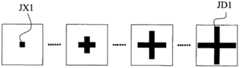
图8是平面雪花状的金属微结构的拓扑图案的演变的第一阶段;Figure 8 is the first stage of the evolution of the topological pattern of the planar snowflake-like metal microstructure;
图9是平面雪花状的金属微结构的拓扑图案的演变的第二阶段。Figure 9 is the second stage of the evolution of the topological pattern of the planar snowflake-like metal microstructure.
具体实施方式Detailed ways
如图1至4所示,根据本发明的卡塞格伦型超材料天线,包括具有中央通孔TK的超材料主反射器ZF、设置在中央通孔TK中的馈源1及设置在馈源1前方的副反射器FF,馈源1辐射的电磁波依次经过副反射器FF、超材料主反射器ZF的反射后以平面波的形式出射,所述超材料主反射器ZF包括核心层100及设置在核心层100后表面的反射层200,所述核心层100包括至少一个核心层片层10,所述核心层片层10包括基材JC以及设置在基材JC上的多个人造微结构2,所述副反射器FF为旋转椭球面的其中一个曲面,所述馈源1的相位中心与旋转椭球面的远焦点F2重合。馈源1的相位中心即为电磁波在馈源中相位相等的点,也就是将馈源等效为理想点源,该理想点源所处的位置,即图中的F2点。As shown in Figures 1 to 4, the Cassegrain-type metamaterial antenna according to the present invention includes a metamaterial main reflector ZF with a central through hole TK, a feed source 1 arranged in the central through hole TK, and a feed source 1 arranged in the central through hole TK. The sub-reflector FF in front, the electromagnetic waves radiated by the feed source 1 are emitted in the form of plane waves after being reflected by the sub-reflector FF and the metamaterial main reflector ZF in turn. The metamaterial main reflector ZF includes a core layer 100 and is arranged on The reflective layer 200 on the back surface of the core layer 100, the core layer 100 includes at least one
本发明中,所述旋转椭球面的实轴Z1垂直超材料主反射器ZF。旋转椭球面的实轴Z1即为焦轴,即为旋转椭球面的近焦点F1与远焦点F2连线所在的直线。近焦点F1靠近副反射器FF,远焦点F2与馈源1的相位中心重合。In the present invention, the real axis Z1 of the spheroid is perpendicular to the main metamaterial reflector ZF. The real axis Z1 of the spheroid is the focal axis, which is the straight line connecting the near focus F1 and the far focus F2 of the spheroid. The near focus F1 is close to the sub-reflector FF, and the far focus F2 coincides with the phase center of the feed 1 .
本发明中,优选地,所述馈源1为波纹喇叭,所述旋转椭球面的实轴通过波纹喇叭的口径面的中心。In the present invention, preferably, the feed source 1 is a corrugated horn, and the real axis of the ellipsoid of revolution passes through the center of the aperture surface of the corrugated horn.
本发明中,反射层可以为具有光滑的表面的金属反射板,例如可以是抛光的铜板、铝板或铁板等,也可是PEC(理想电导体)反射面,当然也可以是金属涂层,例如铜涂层。本发明中,所述核心层片层10任一纵截面具有相同的形状与面积,此处的纵截面是指核心层片层10中与所述旋转椭球面的实轴垂直的剖面。所述核心层片层的纵截面可以是为方形,也可是圆形或者椭圆形,例如300×300mm或450×450mm的正方形,或者直径为250、300或450mm的圆形。In the present invention, the reflective layer can be a metal reflective plate with a smooth surface, such as a polished copper plate, aluminum plate or iron plate, etc., or a PEC (Perfect Electric Conductor) reflective surface, of course it can also be a metal coating, such as Copper coating. In the present invention, any longitudinal section of the
本发明中,任一核心层片层10的折射率分布满足如下公式:In the present invention, the refractive index distribution of any
其中,n(r)表示该核心层片层10上半径为r处的折射率值,该核心层片层的折射率分布圆心即为旋转椭球面的实轴与该核心层片层的交点;Wherein, n(r) represents the refractive index value at the radius r on the
s为所述旋转椭球面的近焦点到超材料主反射器的前表面的距离;s is the distance from the near focus of the spheroid to the front surface of the metamaterial main reflector;
d为核心层的厚度;d is the thickness of the core layer;
nmax表示核心层片层上的折射率最大值;nmax represents the maximum value of the refractive index on the core layer sheet;
nmin表示核心层片层上的折射率最小值;nmin represents the minimum value of the refractive index on the core layer sheet;
λ表示天线中心频率对应的电磁波的波长;λ represents the wavelength of the electromagnetic wave corresponding to the center frequency of the antenna;
floor表示向下取整数;floor means rounding down to an integer;
例如,当

本发明中,为了便于理解,如图4所示,可以将所述核心层片层10划分为矩形阵列排布的多个如图2所示的超材料单元D,每个超材料单元D包括前基板单元U、后基板单元V及设置在前基板单元U、后基板单元V之间的人造微结构2,通常超材料单元D的长、宽及厚度均不大于天线中心频率对应的电磁波的波长的五分之一,优选为十分之一,因此,根据天线的中心频率可以确定超材料单元D的尺寸。图2为透视的画法,以表示人造微结构在超材料单元D中的位置,如图2所示,所述人造微结构2夹于基板单元U、后基板单元V之间,其所在表面用SR表示。In the present invention, for ease of understanding, as shown in Figure 4, the
由公式(1)至公式(3)所确定的核心层片层,沿其法线方向折射率保持不变,在垂直于法线的平面内其折射率分布如图3所示,其包括多个共心的环形区域,其圆心为图中的O点,优选地,圆心即为该平面的中心,图3中示意性的画出了环形区域H1至环形区域H6,每一环形区域内相同半径r处的折射率相等,且随着半径r的增大折射逐渐减小,且有相邻两个环形区域在其相接的位置折射率呈跳变形式,即相邻两个环形区域中,位于内侧的环形区域其最外侧的折射率为nmin,位于外侧的环形区域其最内侧的折射率为nmax,例如,图3中,环形区域H1最外侧的折射率为nmin,环形区域H2最内侧的折射率为nmax。应当注意,环形区域不一定是完整的,也可以是不完整的,例如图3中的环形区域H5及H6,只有当核心层片层10的纵截面为圆形时,其得到的多个环形区域则均为完整的环形区域。The refractive index of the core layer determined by formula (1) to formula (3) remains unchanged along the normal direction, and its refractive index distribution in the plane perpendicular to the normal is shown in Figure 3, which includes multiple A concentric annular area, the center of which is the O point in the figure, preferably, the center of circle is the center of the plane, schematically drawing the annular area H1 to the annular area H6 in Fig. 3, the same in each annular area The refractive index at the radius r is equal, and the refraction gradually decreases with the increase of the radius r, and there are two adjacent annular areas where the refractive index jumps in the form of a jump, that is, in the adjacent two annular areas , the outermost refractive index of the inner annular region is nmin , and the innermost refractive index of the outer annular region is nmax , for example, in Figure 3, the outermost refractive index of the annular region H1 is nmin , the annular The innermost refractive index of the region H2 is nmax . It should be noted that the annular regions are not necessarily complete, and may also be incomplete, such as the annular regions H5 and H6 in FIG. The area is a complete ring area.
本发明中,上述的半径r是指图3中的圆心O到每一超材料单元的表面中心的距离,上述的半径严格意义上并不是一个连续的变化范围,但是由于每一个超材料单元都是远远小于天线中心频率对应的电磁波的波长,所以可以近似的认为上述的半径是连续变化的。In the present invention, the above-mentioned radius r refers to the distance from the center of circle O in Fig. 3 to the surface center of each metamaterial unit, and the above-mentioned radius is not a continuous range of variation in the strict sense, but since each metamaterial unit is much smaller than the wavelength of the electromagnetic wave corresponding to the center frequency of the antenna, so it can be approximated that the above-mentioned radius changes continuously.
由公式(1)至公式(3)所确定的核心层片层,具有如图3所示的折射率分布规律,根据天线中心频率,合理设计核心层片层的层数(即核心层的厚度),即可以使得由所述旋转椭球面的近焦点F1发出的电磁波经超材料主反射器后能够以垂直于核心层片层的平面波的形式出射,即超材料主反射器的焦点与所述旋转椭球面的近焦点F1重合。The core layer determined by formula (1) to formula (3) has the distribution law of refractive index as shown in Figure 3. According to the antenna center frequency, the number of layers of the core layer (that is, the thickness of the core layer) is reasonably designed. ), that is, the electromagnetic wave emitted by the near focal point F1 of the spheroid surface can be emitted in the form of a plane wave perpendicular to the core layer after passing through the metamaterial main reflector, that is, the focal point of the metamaterial main reflector and the The near focus F1 of the spheroids of revolution coincides.
根据公知常识可以得到,由馈源1的相位中心(即远焦点F2)发出的电磁波其在旋转椭球面的一个曲面(副反射器)上反射后的电磁波必然经过近焦点F1,这样,如果设计近焦点F1为超材料主反射器的焦点就能够使得经超材料主反射器反射后的电磁波以平面波的形式出射;反之亦然,即垂直超材料主反射器入射的平面电磁波能够在馈源的相位中心处(也即远焦点F2处)聚焦。According to common knowledge, it can be obtained that the electromagnetic wave emitted by the phase center of the feed source 1 (i.e. the far focus F2) is reflected on a curved surface (sub-reflector) of the spheroid must pass through the near focus F1, so if the design If the near focal point F1 is the focal point of the metamaterial main reflector, the electromagnetic waves reflected by the metamaterial main reflector can emerge in the form of plane waves; Focus at the phase center (that is, at the far focal point F2).
本发明中,优选地,所述副反射器曲面形状与面积适应主反射器的形状与面积,即如图1所示,使得由副反射器边缘出射的电磁波刚好到达主反射器的边缘。In the present invention, preferably, the shape and area of the curved surface of the sub-reflector adapt to the shape and area of the main reflector, that is, as shown in FIG. 1 , so that the electromagnetic wave emitted from the edge of the sub-reflector just reaches the edge of the main reflector.
本发明中,如图4所示,所述基材JC包括片状的前基板13及后基板15,所述多个人造微结构夹设在前基板13与后基板15之间,所述核心层片层的厚度为0.21-2.5mm,其中,前基板的厚度为0.1-1mm,后基板的厚度为0.1-1mm,多个人造微结构2的厚度为0.01-0.5mm。In the present invention, as shown in FIG. 4 , the substrate JC includes a sheet-shaped
作为一个例子,所述核心层片层的厚度为0.818mm,其中,前基板与后基板的厚度均为0.4mm,多个人造微结构的厚度为0.018mm。As an example, the thickness of the core layer is 0.818mm, wherein the thickness of the front substrate and the rear substrate are both 0.4mm, and the thickness of the plurality of artificial microstructures is 0.018mm.
每一核心层片层的厚度确定了,则可以根据需要设定不同的层数,从而形成具有厚度d的核心层。Once the thickness of each core layer is determined, different numbers of layers can be set according to needs, so as to form a core layer with a thickness d.
本发明中,所述基材由陶瓷材料、聚苯乙烯、聚丙烯、聚酰亚胺、聚乙烯、聚醚醚酮或聚四氟乙烯制得。例如,聚四氟乙烯板(PS板),其具有很好的电绝缘性,不会对电磁波的电场产生干扰,并且具有优良的化学稳定性、耐腐蚀性,使用寿命长。In the present invention, the substrate is made of ceramic material, polystyrene, polypropylene, polyimide, polyethylene, polyether ether ketone or polytetrafluoroethylene. For example, polytetrafluoroethylene board (PS board), which has good electrical insulation, will not interfere with the electric field of electromagnetic waves, and has excellent chemical stability, corrosion resistance, and long service life.
本发明中,优选地,所述人造微结构2为金属微结构,所述金属微结构由一条或多条金属线组成,所述金属线为铜线、银线或者铝线,所述基材JC上的多个人造微结构通过蚀刻、电镀、钻刻、光刻、电子刻或离子刻的方法得到。例如图4所示的核心层片层,可以先通过在前基板13或后基板15中的其中一个上覆铜,再通过蚀刻等工艺去掉不需要的铜,即得到了多个人造微结构的平面排布,最后用热熔胶将前基板与后基板粘合在一起即形成了一个核心层片。通过上述方法可以形成多个核心层片层,将各个核心层片层用热熔胶粘接即可得到多层的核心层。热熔胶的材料最好与核心层片层的材料保持一致。In the present invention, preferably, the
本发明中,优选地,所述基材上的多个人造微结构由图5所示的呈平面雪花状的金属微结构的拓扑图案的演变得到。即图5所示的金属微结构的拓扑图案为呈平面雪花状的金属微结构的基本平面拓扑图案,同一基材上的所有金属微结构的拓扑图案均由图5所示的图案演变得到。In the present invention, preferably, the multiple artificial microstructures on the substrate are obtained from the evolution of the topological pattern of the planar snowflake-shaped metal microstructure shown in FIG. 5 . That is, the topological pattern of the metal microstructure shown in FIG. 5 is the basic planar topological pattern of the metal microstructure in the shape of a plane snowflake, and the topological patterns of all metal microstructures on the same substrate are evolved from the pattern shown in FIG. 5 .
如图5所示,所述呈平面雪花状的金属微结构具有相互垂直平分的第一金属线J1及第二金属线J2,所述第一金属线J1与第二金属线J2的长度相同,所述第一金属线J1两端连接有相同长度的两个第一金属分支F1,所述第一金属线J1两端连接在两个第一金属分支F1的中点上,所述第二金属线J2两端连接有相同长度的两个第二金属分支F2,所述第二金属线J2两端连接在两个第二金属分支F2的中点上,所述第一金属分支F1与第二金属分支F2的长度相等。As shown in FIG. 5 , the metal microstructure in the shape of a plane snowflake has a first metal line J1 and a second metal line J2 that are perpendicular to each other, and the lengths of the first metal line J1 and the second metal line J2 are the same. Both ends of the first metal line J1 are connected to two first metal branches F1 of the same length, both ends of the first metal line J1 are connected to the midpoint of the two first metal branches F1, and the second metal The two ends of the line J2 are connected with two second metal branches F2 of the same length, the two ends of the second metal line J2 are connected at the midpoint of the two second metal branches F2, the first metal branch F1 and the second The lengths of the metal branches F2 are equal.
图6是图5所示的平面雪花状的金属微结构的一种衍生结构。其在每个第一金属分支F1及每个第二金属分支F2的两端均连接有完全相同的第三金属分支F3,并且相应的第三金属分支F3的中点分别与第一金属分支F1及第二金属分支F2的端点相连。依此类推,本发明还可以衍生出其它形式的金属微结构。同样,图6所示的只是基本平面拓扑图案。FIG. 6 is a derivative structure of the planar snowflake-like metal microstructure shown in FIG. 5 . Both ends of each first metal branch F1 and each second metal branch F2 are connected to identical third metal branches F3, and the midpoints of the corresponding third metal branches F3 are respectively connected to the first metal branch F1. and the terminal of the second metal branch F2 are connected. By analogy, the present invention can also derive other forms of metal microstructures. Again, what is shown in Figure 6 is only the basic planar topological pattern.
图7是图5所示的平面雪花状的金属微结构的一种变形结构,此种结构的金属微结构,第一金属线J1与第二金属线J2不是直线,而是弯折线,第一金属线J1与第二金属线J2均设置有两个弯折部WZ,但是第一金属线J1与第二金属线J2仍然是垂直平分,通过设置弯折部的朝向与弯折部在第一金属线与第二金属线上的相对位置,使得图7所示的金属微结构绕垂直于第一金属线与第二金属线交点的轴线向任意方向旋转90度的图形都与原图重合。另外,还可以有其它变形,例如,第一金属线J1与第二金属线J2均设置多个弯折部WZ。同样,图7所示的只是基本平面拓扑图案。FIG. 7 is a deformed structure of the plane snowflake-shaped metal microstructure shown in FIG. Both the metal wire J1 and the second metal wire J2 are provided with two bending parts WZ, but the first metal wire J1 and the second metal wire J2 are still perpendicularly bisected. The relative position of the metal line and the second metal line makes the pattern of the metal microstructure shown in FIG. 7 rotated 90 degrees in any direction around the axis perpendicular to the intersection of the first metal line and the second metal line coincide with the original figure. In addition, other deformations are also possible, for example, the first metal line J1 and the second metal line J2 are both provided with a plurality of bent portions WZ. Likewise, what is shown in Figure 7 is only the basic planar topological pattern.
已知折射率
本实施例中,核心层片层上的人造微结构的平面排布可通过计算机仿真(例如CST仿真)得到,具体如下:In this embodiment, the planar arrangement of the artificial microstructure on the core layer sheet can be obtained by computer simulation (such as CST simulation), as follows:
(1)确定人造微结构的附着基材。例如介电常数为2.7的介质基板,该介质基板的材料可以是FR-4、F4b或PS。(1) Determine the attachment substrate of the artificial microstructure. For example, a dielectric substrate with a dielectric constant of 2.7, the material of the dielectric substrate may be FR-4, F4b or PS.
(2)确定超材料单元的尺寸。超材料单元的尺寸由天线的中心频率得到,利用频率得到其波长,再取小于波长的五分之一的一个数值做为超材料单元D的长度CD与宽度KD,再取小于波长的十分之一的一个数值做为超材料单元D厚度。例如对应于11.95G的天线中心频率,所述超材料单元D为如图2所示的长CD与宽KD均为2.8mm、厚度HD为0.543mm的方形小板。(2) Determine the size of the metamaterial unit. The size of the metamaterial unit is obtained from the center frequency of the antenna, its wavelength is obtained by using the frequency, and then a value less than one-fifth of the wavelength is taken as the length CD and width KD of the metamaterial unit D, and then a value less than one-fifth of the wavelength is taken as A value of one of is used as the thickness of the metamaterial element D. For example, corresponding to the antenna center frequency of 11.95G, the metamaterial unit D is a small square plate with a length CD and a width KD of 2.8 mm and a thickness HD of 0.543 mm as shown in FIG. 2 .
(3)确定人造微结构的材料及其基本平面拓扑图案。本发明中,人造微结构为金属微结构,所述金属微结构的材料为铜,金属微结构的基本平面拓扑图案为图5所示的平面雪花状的金属微结构,其线宽W各处一致;此处的基本平面拓扑图案,是指同一基材上的所有人造微结构的拓扑图案的演变基础。(3) Determine the materials and basic planar topological patterns of artificial microstructures. In the present invention, the artificial microstructure is a metal microstructure, and the material of the metal microstructure is copper, and the basic planar topological pattern of the metal microstructure is a plane snowflake-like metal microstructure as shown in Figure 5, and its line width W is everywhere Consistent; the basic planar topological pattern here refers to the evolution basis of the topological patterns of all artificial microstructures on the same substrate.
(4)确定人造微结构的拓扑图案参数。如图5所示,本发明中,平面雪花状的金属微结构的拓扑图案参数包括金属微结构的线宽W,第一金属线J1的长度a,第一金属分支F1的长度b,及金属微结构的厚度HD,本发明中,厚度不变,取为0.018mm。(4) Determine the topological pattern parameters of the artificial microstructure. As shown in Figure 5, in the present invention, the topological pattern parameter of the metal microstructure of plane snowflake shape comprises the line width W of metal microstructure, the length a of the first metal line J1, the length b of the first metal branch F1, and the metal microstructure. The thickness HD of the microstructure, in the present invention, does not change, and is taken as 0.018 mm.
(5)确定金属微结构的拓扑图案的演变限制条件。本发明中,金属微结构的拓扑图案的演变限制条件有,金属微结构之间的最小间距WL(即如图5所示,金属微结构与超材料单元的长边或宽边的距离为WL/2),金属微结构的线宽W,超材料单元的尺寸;由于加工工艺限制,WL大于等于0.1mm,同样,线宽W也是要大于等于0.1mm。第一次仿真时,WL可以取0.1mm,W可以取0.3mm,超材料单元的尺寸为长与宽为2.8mm,厚度为0.818mm(金属微结构的厚度为0.018mm,基材的厚度为0.8mm),此时金属微结构的拓扑图案参数只有a和b两个变量。金属微结构的拓扑图案通过如图8至图9所示的演变方式,对应于某一特定频率(例如11.95GHZ),可以得到一个连续的折射率变化范围。(5) To determine the evolution constraints of the topological pattern of the metal microstructure. In the present invention, the evolution constraint condition of the topological pattern of the metal microstructure has, the minimum spacing WL between the metal microstructure (that is, as shown in Figure 5, the distance between the metal microstructure and the long side or wide side of the metamaterial unit is WL /2), the line width W of the metal microstructure, and the size of the metamaterial unit; due to the limitation of the processing technology, WL is greater than or equal to 0.1mm, and similarly, the line width W must also be greater than or equal to 0.1mm. In the first simulation, WL can be taken as 0.1mm, and W can be taken as 0.3mm. The size of the metamaterial unit is 2.8mm in length and width, and 0.818mm in thickness (the thickness of the metal microstructure is 0.018mm, and the thickness of the substrate is 0.8mm), at this time, the topological pattern parameters of the metal microstructure only have two variables, a and b. The topological pattern of the metal microstructure corresponds to a specific frequency (for example, 11.95GHZ) through the evolution as shown in FIG. 8 to FIG. 9 , and a continuous range of refractive index variation can be obtained.
具体地,所述金属微结构的拓扑图案的演变包括两个阶段(拓扑图案演变的基本图案为图5所示的金属微结构):Specifically, the evolution of the topological pattern of the metal microstructure includes two stages (the basic pattern of topological pattern evolution is the metal microstructure shown in Figure 5):
第一阶段:根据演变限制条件,在b值保持不变的情况下,将a值从最小值变化到最大值,此演变过程中的金属微结构均为“十”字形(a取最小值时除外)。本实施例中,a的最小值即为0.3mm(线宽W),a的最大值为(CD-WL)。因此,在第一阶段中,金属微结构的拓扑图案的演变如图8所示,即从边长为W的正方形JX1,逐渐演变成最大的“十”字形拓扑图案JD1。在第一阶段中,随着金属微结构的拓扑图案的演变,与其对应的超材料单元的折射率连续增大(对应天线一特定频率)。The first stage: According to the evolution constraints, under the condition that the value of b remains unchanged, the value of a is changed from the minimum value to the maximum value. except). In this embodiment, the minimum value of a is 0.3 mm (line width W), and the maximum value of a is (CD-WL). Therefore, in the first stage, the evolution of the topological pattern of the metal microstructure is shown in Figure 8, that is, from a square JX1 with side length W to the largest topological pattern JD1 of a "cross". In the first stage, as the topological pattern of the metal microstructure evolves, the refractive index of the corresponding metamaterial unit increases continuously (corresponding to a specific frequency of the antenna).
第二阶段:根据演变限制条件,当a增加到最大值时,a保持不变;此时,将b从最小值连续增加到最大值,此演变过程中的金属微结构均为平面雪花状。本实施例中,b的最小值即为0.3mm,b的最大值为(CD-WL-2W)。因此,在第二阶段中,金属微结构的拓扑图案的演变如图9所示,即从最大的“十”字形拓扑图案JD1,逐渐演变成最大的平面雪花状的拓扑图案JD2,此处的最大的平面雪花状的拓扑图案JD2是指,第一金属分支J1与第二金属分支J2的长度b已经不能再伸长,否则第一金属分支与第二金属分支将发生相交。在第二阶段中,随着金属微结构的拓扑图案的演变,与其对应的超材料单元的折射率连续增大(对应天线一特定频率)。The second stage: According to the evolution constraints, when a increases to the maximum value, a remains unchanged; at this time, b is continuously increased from the minimum value to the maximum value, and the metal microstructure in this evolution process is planar snowflake shape. In this embodiment, the minimum value of b is 0.3 mm, and the maximum value of b is (CD-WL-2W). Therefore, in the second stage, the evolution of the topological pattern of the metal microstructure is shown in Fig. 9, that is, from the largest "cross" topological pattern JD1, to the largest planar snowflake-like topological pattern JD2, where The largest planar snowflake-like topological pattern JD2 means that the length b of the first metal branch J1 and the second metal branch J2 can no longer be extended, otherwise the first metal branch and the second metal branch will intersect. In the second stage, as the topological pattern of the metal microstructure evolves, the refractive index of the corresponding metamaterial unit increases continuously (corresponding to a specific frequency of the antenna).
通过上述演变得到超材料单元的折射率变化范围如果包含了nmin至nmax的连续变化范围,则满足设计需要。如果上述演变得到超材料单元的折射率变化范围不满足设计需要,例如最大值太小或最小值过大,则变动WL与W,重新仿真,直到得到我们需要的折射率变化范围。Through the above evolution, if the refractive index variation range of the metamaterial unit includes the continuous variation range from nmin to nmax , it will meet the design requirements. If the range of refractive index variation of the metamaterial unit obtained from the above evolution does not meet the design requirements, for example, the maximum value is too small or the minimum value is too large, then change WL and W, and re-simulate until the desired range of refractive index variation is obtained.
根据公式(1)至(3),将仿真得到的一系列的超材料单元按照其对应的折射率排布以后(实际上就是不同拓扑图案的多个人造微结构在基材上的排布),即能得到本发明的核心层片层。According to the formulas (1) to (3), the simulated series of metamaterial units are arranged according to their corresponding refractive indices (in fact, it is the arrangement of multiple artificial microstructures with different topological patterns on the substrate) , that is, the core layer sheet of the present invention can be obtained.
上面结合附图对本发明的实施例进行了描述,但是本发明并不局限于上述的具体实施方式,上述的具体实施方式仅仅是示意性的,而不是限制性的,本领域的普通技术人员在本发明的启示下,在不脱离本发明宗旨和权利要求所保护的范围情况下,还可做出很多形式,这些均属于本发明的保护之内。Embodiments of the present invention have been described above in conjunction with the accompanying drawings, but the present invention is not limited to the above-mentioned specific implementations, and the above-mentioned specific implementations are only illustrative, rather than restrictive, and those of ordinary skill in the art will Under the enlightenment of the present invention, many forms can also be made without departing from the gist of the present invention and the protection scope of the claims, and these all belong to the protection of the present invention.
Claims (10)
Translated fromChinesePriority Applications (4)
| Application Number | Priority Date | Filing Date | Title |
|---|---|---|---|
| CN201210269062.3ACN102856664B (en) | 2012-07-31 | 2012-07-31 | Cassegrain type metamaterial antenna |
| EP13826029.4AEP2882038B1 (en) | 2012-07-31 | 2013-07-31 | Cassegrain-type metamaterial antenna |
| PCT/CN2013/080576WO2014019524A1 (en) | 2012-07-31 | 2013-07-31 | Cassegrain-type metamaterial antenna |
| US14/607,463US9742074B2 (en) | 2012-07-31 | 2015-01-28 | Cassegrain-type metamaterial antenna |
Applications Claiming Priority (1)
| Application Number | Priority Date | Filing Date | Title |
|---|---|---|---|
| CN201210269062.3ACN102856664B (en) | 2012-07-31 | 2012-07-31 | Cassegrain type metamaterial antenna |
Publications (2)
| Publication Number | Publication Date |
|---|---|
| CN102856664Atrue CN102856664A (en) | 2013-01-02 |
| CN102856664B CN102856664B (en) | 2015-07-01 |
Family
ID=47403010
Family Applications (1)
| Application Number | Title | Priority Date | Filing Date |
|---|---|---|---|
| CN201210269062.3AActiveCN102856664B (en) | 2012-07-31 | 2012-07-31 | Cassegrain type metamaterial antenna |
Country Status (1)
| Country | Link |
|---|---|
| CN (1) | CN102856664B (en) |
Cited By (5)
| Publication number | Priority date | Publication date | Assignee | Title |
|---|---|---|---|---|
| WO2014019524A1 (en)* | 2012-07-31 | 2014-02-06 | 深圳光启创新技术有限公司 | Cassegrain-type metamaterial antenna |
| WO2017016207A1 (en)* | 2015-07-24 | 2017-02-02 | 深圳光启高等理工研究院 | Reflecting antenna and design method therefor |
| CN108767489A (en)* | 2018-05-24 | 2018-11-06 | 西安电子科技大学 | Transmission-type Cassegrain antenna based on super surface |
| CN108832311A (en)* | 2018-06-08 | 2018-11-16 | 西安电子科技大学 | Planar Cassegrain Vortex Field Antenna Based on Metasurface |
| CN108832305B (en)* | 2018-06-08 | 2020-08-11 | 西安电子科技大学 | Cassegrain vortex field antenna based on super surface |
Citations (6)
| Publication number | Priority date | Publication date | Assignee | Title |
|---|---|---|---|---|
| CN2408577Y (en)* | 2000-03-02 | 2000-11-29 | 寰波科技股份有限公司 | Parabolic reflector antenna |
| CN102480033A (en)* | 2011-07-26 | 2012-05-30 | 深圳光启高等理工研究院 | Offset feed type microwave antenna |
| CN102480024A (en)* | 2011-07-26 | 2012-05-30 | 深圳光启高等理工研究院 | Feed-backward type radar antenna |
| CN102480032A (en)* | 2011-07-26 | 2012-05-30 | 深圳光启高等理工研究院 | Offset feed type radar antenna |
| CN102480064A (en)* | 2011-07-26 | 2012-05-30 | 深圳光启高等理工研究院 | Feedforward type satellite television antenna and satellite television receiving system thereof |
| CN102593594A (en)* | 2012-02-29 | 2012-07-18 | 深圳光启创新技术有限公司 | Off-set feed type satellite television antenna and satellite television receiving system thereof |
- 2012
- 2012-07-31CNCN201210269062.3Apatent/CN102856664B/enactiveActive
Patent Citations (6)
| Publication number | Priority date | Publication date | Assignee | Title |
|---|---|---|---|---|
| CN2408577Y (en)* | 2000-03-02 | 2000-11-29 | 寰波科技股份有限公司 | Parabolic reflector antenna |
| CN102480033A (en)* | 2011-07-26 | 2012-05-30 | 深圳光启高等理工研究院 | Offset feed type microwave antenna |
| CN102480024A (en)* | 2011-07-26 | 2012-05-30 | 深圳光启高等理工研究院 | Feed-backward type radar antenna |
| CN102480032A (en)* | 2011-07-26 | 2012-05-30 | 深圳光启高等理工研究院 | Offset feed type radar antenna |
| CN102480064A (en)* | 2011-07-26 | 2012-05-30 | 深圳光启高等理工研究院 | Feedforward type satellite television antenna and satellite television receiving system thereof |
| CN102593594A (en)* | 2012-02-29 | 2012-07-18 | 深圳光启创新技术有限公司 | Off-set feed type satellite television antenna and satellite television receiving system thereof |
Non-Patent Citations (2)
| Title |
|---|
| DAVID M.POZAR: "design of millimeter wave microstrip reflectarrays", 《IEEE TRANSACTIONS ON ANTENNAS AND PROPAGATION》* |
| 林曙光: "用于"C/Ku波段双馈源卫星通信天线副反射面"的FSS设计", 《2009年全国微波毫米波会议论文集(上册)》* |
Cited By (8)
| Publication number | Priority date | Publication date | Assignee | Title |
|---|---|---|---|---|
| WO2014019524A1 (en)* | 2012-07-31 | 2014-02-06 | 深圳光启创新技术有限公司 | Cassegrain-type metamaterial antenna |
| US9742074B2 (en) | 2012-07-31 | 2017-08-22 | Kuang-Chi Innovative Technology Ltd. | Cassegrain-type metamaterial antenna |
| WO2017016207A1 (en)* | 2015-07-24 | 2017-02-02 | 深圳光启高等理工研究院 | Reflecting antenna and design method therefor |
| CN108767489A (en)* | 2018-05-24 | 2018-11-06 | 西安电子科技大学 | Transmission-type Cassegrain antenna based on super surface |
| CN108767489B (en)* | 2018-05-24 | 2020-04-07 | 西安电子科技大学 | Transmission type Cassegrain antenna based on super surface |
| CN108832311A (en)* | 2018-06-08 | 2018-11-16 | 西安电子科技大学 | Planar Cassegrain Vortex Field Antenna Based on Metasurface |
| CN108832305B (en)* | 2018-06-08 | 2020-08-11 | 西安电子科技大学 | Cassegrain vortex field antenna based on super surface |
| CN108832311B (en)* | 2018-06-08 | 2020-08-11 | 西安电子科技大学 | Metasurface-based planar Cassegrain vortex field antenna |
Also Published As
| Publication number | Publication date |
|---|---|
| CN102856664B (en) | 2015-07-01 |
Similar Documents
| Publication | Publication Date | Title |
|---|---|---|
| CN102800995B (en) | A metamaterial antenna | |
| US9742074B2 (en) | Cassegrain-type metamaterial antenna | |
| CN102800994B (en) | Cassegrain type metamaterial antenna | |
| CN102856664B (en) | Cassegrain type metamaterial antenna | |
| CN104681981A (en) | Integrated short backfire antenna of millimeter wave dielectrics | |
| CN102820555B (en) | Cassegrain metamaterial antenna | |
| CN102593606B (en) | Metamaterial antenna of inclined reflect sheet and satellite television receiving system | |
| CN103094705B (en) | Lens antenna based on Meta Materials | |
| CN102680802B (en) | Compact range generation device | |
| CN103682665A (en) | Metamaterial microwave antenna | |
| CN103036064B (en) | A kind of Cassegrain metamaterial antenna | |
| CN102544743A (en) | Microwave antenna | |
| CN103094711B (en) | A kind of lens antenna | |
| CN103296417B (en) | Metamaterial antenna cover and antenna system | |
| CN103094710B (en) | Super-material antenna | |
| CN102683811B (en) | Metamaterial satellite antenna and satellite receiving system | |
| CN102842766B (en) | Metamaterial microwave antenna | |
| CN102709709B (en) | metamaterial antenna | |
| CN103036065B (en) | A kind of Cassegrain metamaterial antenna | |
| CN103296458B (en) | A kind of antenna for satellite communication in motion | |
| CN103293393B (en) | Compact range generating device | |
| CN103293392B (en) | A kind of Compact range generation device | |
| CN103682663B (en) | A kind of metamaterial microwave antenna | |
| CN103036028B (en) | A kind of electromagnetic horn | |
| CN103682671B (en) | A kind of metamaterial microwave antenna |
Legal Events
| Date | Code | Title | Description |
|---|---|---|---|
| C06 | Publication | ||
| PB01 | Publication | ||
| C10 | Entry into substantive examination | ||
| SE01 | Entry into force of request for substantive examination | ||
| C14 | Grant of patent or utility model | ||
| GR01 | Patent grant | ||
| TR01 | Transfer of patent right | Effective date of registration:20210407 Address after:2 / F, software building, No.9, Gaoxin Zhongyi Road, Nanshan District, Shenzhen City, Guangdong Province Patentee after:KUANG-CHI INSTITUTE OF ADVANCED TECHNOLOGY Address before:18B, building a, CIC international business center, 1061 Xiangmei Road, Futian District, Shenzhen, Guangdong 518034 Patentee before:KUANG-CHI INNOVATIVE TECHNOLOGY Ltd. | |
| TR01 | Transfer of patent right |