CN102843025A - Control circuit, control method and power supply system for PFC circuit - Google Patents
Control circuit, control method and power supply system for PFC circuitDownload PDFInfo
- Publication number
- CN102843025A CN102843025ACN2012102844392ACN201210284439ACN102843025ACN 102843025 ACN102843025 ACN 102843025ACN 2012102844392 ACN2012102844392 ACN 2012102844392ACN 201210284439 ACN201210284439 ACN 201210284439ACN 102843025 ACN102843025 ACN 102843025A
- Authority
- CN
- China
- Prior art keywords
- signal
- switch
- circuit
- digital signal
- input terminal
- Prior art date
- Legal status (The legal status is an assumption and is not a legal conclusion. Google has not performed a legal analysis and makes no representation as to the accuracy of the status listed.)
- Granted
Links
Images


Classifications
- H—ELECTRICITY
- H02—GENERATION; CONVERSION OR DISTRIBUTION OF ELECTRIC POWER
- H02M—APPARATUS FOR CONVERSION BETWEEN AC AND AC, BETWEEN AC AND DC, OR BETWEEN DC AND DC, AND FOR USE WITH MAINS OR SIMILAR POWER SUPPLY SYSTEMS; CONVERSION OF DC OR AC INPUT POWER INTO SURGE OUTPUT POWER; CONTROL OR REGULATION THEREOF
- H02M1/00—Details of apparatus for conversion
- H02M1/0083—Converters characterised by their input or output configuration
- H02M1/0085—Partially controlled bridges
- G—PHYSICS
- G05—CONTROLLING; REGULATING
- G05F—SYSTEMS FOR REGULATING ELECTRIC OR MAGNETIC VARIABLES
- G05F1/00—Automatic systems in which deviations of an electric quantity from one or more predetermined values are detected at the output of the system and fed back to a device within the system to restore the detected quantity to its predetermined value or values, i.e. retroactive systems
- G05F1/70—Regulating power factor; Regulating reactive current or power
- H—ELECTRICITY
- H02—GENERATION; CONVERSION OR DISTRIBUTION OF ELECTRIC POWER
- H02M—APPARATUS FOR CONVERSION BETWEEN AC AND AC, BETWEEN AC AND DC, OR BETWEEN DC AND DC, AND FOR USE WITH MAINS OR SIMILAR POWER SUPPLY SYSTEMS; CONVERSION OF DC OR AC INPUT POWER INTO SURGE OUTPUT POWER; CONTROL OR REGULATION THEREOF
- H02M1/00—Details of apparatus for conversion
- H02M1/42—Circuits or arrangements for compensating for or adjusting power factor in converters or inverters
- H02M1/4208—Arrangements for improving power factor of AC input
- H02M1/4225—Arrangements for improving power factor of AC input using a non-isolated boost converter
- H—ELECTRICITY
- H02—GENERATION; CONVERSION OR DISTRIBUTION OF ELECTRIC POWER
- H02M—APPARATUS FOR CONVERSION BETWEEN AC AND AC, BETWEEN AC AND DC, OR BETWEEN DC AND DC, AND FOR USE WITH MAINS OR SIMILAR POWER SUPPLY SYSTEMS; CONVERSION OF DC OR AC INPUT POWER INTO SURGE OUTPUT POWER; CONTROL OR REGULATION THEREOF
- H02M3/00—Conversion of DC power input into DC power output
- H02M3/02—Conversion of DC power input into DC power output without intermediate conversion into AC
- H02M3/04—Conversion of DC power input into DC power output without intermediate conversion into AC by static converters
- H02M3/10—Conversion of DC power input into DC power output without intermediate conversion into AC by static converters using discharge tubes with control electrode or semiconductor devices with control electrode
- H02M3/145—Conversion of DC power input into DC power output without intermediate conversion into AC by static converters using discharge tubes with control electrode or semiconductor devices with control electrode using devices of a triode or transistor type requiring continuous application of a control signal
- H02M3/155—Conversion of DC power input into DC power output without intermediate conversion into AC by static converters using discharge tubes with control electrode or semiconductor devices with control electrode using devices of a triode or transistor type requiring continuous application of a control signal using semiconductor devices only
- H02M3/156—Conversion of DC power input into DC power output without intermediate conversion into AC by static converters using discharge tubes with control electrode or semiconductor devices with control electrode using devices of a triode or transistor type requiring continuous application of a control signal using semiconductor devices only with automatic control of output voltage or current, e.g. switching regulators
- H—ELECTRICITY
- H02—GENERATION; CONVERSION OR DISTRIBUTION OF ELECTRIC POWER
- H02M—APPARATUS FOR CONVERSION BETWEEN AC AND AC, BETWEEN AC AND DC, OR BETWEEN DC AND DC, AND FOR USE WITH MAINS OR SIMILAR POWER SUPPLY SYSTEMS; CONVERSION OF DC OR AC INPUT POWER INTO SURGE OUTPUT POWER; CONTROL OR REGULATION THEREOF
- H02M7/00—Conversion of AC power input into DC power output; Conversion of DC power input into AC power output
- H02M7/02—Conversion of AC power input into DC power output without possibility of reversal
- H02M7/04—Conversion of AC power input into DC power output without possibility of reversal by static converters
- H02M7/06—Conversion of AC power input into DC power output without possibility of reversal by static converters using discharge tubes without control electrode or semiconductor devices without control electrode
- Y—GENERAL TAGGING OF NEW TECHNOLOGICAL DEVELOPMENTS; GENERAL TAGGING OF CROSS-SECTIONAL TECHNOLOGIES SPANNING OVER SEVERAL SECTIONS OF THE IPC; TECHNICAL SUBJECTS COVERED BY FORMER USPC CROSS-REFERENCE ART COLLECTIONS [XRACs] AND DIGESTS
- Y02—TECHNOLOGIES OR APPLICATIONS FOR MITIGATION OR ADAPTATION AGAINST CLIMATE CHANGE
- Y02B—CLIMATE CHANGE MITIGATION TECHNOLOGIES RELATED TO BUILDINGS, e.g. HOUSING, HOUSE APPLIANCES OR RELATED END-USER APPLICATIONS
- Y02B70/00—Technologies for an efficient end-user side electric power management and consumption
- Y02B70/10—Technologies improving the efficiency by using switched-mode power supplies [SMPS], i.e. efficient power electronics conversion e.g. power factor correction or reduction of losses in power supplies or efficient standby modes
- Y—GENERAL TAGGING OF NEW TECHNOLOGICAL DEVELOPMENTS; GENERAL TAGGING OF CROSS-SECTIONAL TECHNOLOGIES SPANNING OVER SEVERAL SECTIONS OF THE IPC; TECHNICAL SUBJECTS COVERED BY FORMER USPC CROSS-REFERENCE ART COLLECTIONS [XRACs] AND DIGESTS
- Y02—TECHNOLOGIES OR APPLICATIONS FOR MITIGATION OR ADAPTATION AGAINST CLIMATE CHANGE
- Y02P—CLIMATE CHANGE MITIGATION TECHNOLOGIES IN THE PRODUCTION OR PROCESSING OF GOODS
- Y02P80/00—Climate change mitigation technologies for sector-wide applications
- Y02P80/10—Efficient use of energy, e.g. using compressed air or pressurized fluid as energy carrier
Landscapes
- Engineering & Computer Science (AREA)
- Power Engineering (AREA)
- Physics & Mathematics (AREA)
- Electromagnetism (AREA)
- General Physics & Mathematics (AREA)
- Radar, Positioning & Navigation (AREA)
- Automation & Control Theory (AREA)
- Power Conversion In General (AREA)
- Rectifiers (AREA)
- Electronic Switches (AREA)
- Dc-Dc Converters (AREA)
Abstract
Description
Translated fromChinese技术领域technical field
本发明涉及电力电子技术,尤其涉及一种用于PFC电路的控制电路、控制方法以及含有该控制电路的电源系统。The invention relates to power electronics technology, in particular to a control circuit for a PFC circuit, a control method and a power supply system containing the control circuit.
背景技术Background technique
当前,为了降低电力电子装置频繁使用给电网造成的严重谐波污染,通常需要引入功率因数校正(PFC)电路,藉由PFC电路使输入电流谐波满足预设的谐波要求。此外,PFC电路的发展趋势也如同大部分的电源产品一样,朝着高效率(High efficiency),高功率密度(High power density)方向发展。At present, in order to reduce the serious harmonic pollution caused by the frequent use of power electronic devices to the power grid, it is usually necessary to introduce a power factor correction (PFC) circuit, and use the PFC circuit to make the input current harmonics meet the preset harmonic requirements. In addition, the development trend of PFC circuits, like most power supply products, is developing in the direction of high efficiency and high power density.
以无桥PFC电路拓扑为例,该电路具有低通态损耗、低共模干扰以及元器件利用率高等诸多优点。例如,无桥PFC电路包括彼此并联连接的一第一桥臂和一第二桥臂,第一桥臂由第一MOSFET和第二MOSFET构成,第二桥臂由第一二极管D1和第二二极管D2构成。Taking the bridgeless PFC circuit topology as an example, this circuit has many advantages such as low on-state loss, low common-mode interference, and high utilization of components. For example, a bridgeless PFC circuit includes a first bridge arm and a second bridge arm connected in parallel with each other, the first bridge arm is composed of a first MOSFET and a second MOSFET, and the second bridge arm is composed of a first diode D1 and a second bridge arm. Two diodes D2 form.
当第一桥臂中的第二MOSFET关断,第一MOSFET开通时,电感通过第一MOSFET和第四MOSFET释放能量,电感电流也随之减小。之后,电感电流在某一时刻降低至零,并在该时刻之后电流反向。当第一MOSFET关断后,第二MOSFET的漏极与源极两端的电压(VDS)开始下降,若该电压下降到零的同时,控制第二MOSFET开通,可实现该第二MOSFET的零电压开通,降低开关损耗。然而,采用何种控制机制来实现上述零电压开通,降低电路中的开关损耗,是相关技术人员需要着手解决的一项课题。此外,如何简单有效地对电感电流的过零点进行自动检测,也是设计人员亟待解决的任务。When the second MOSFET in the first bridge arm is turned off and the first MOSFET is turned on, the inductor releases energy through the first MOSFET and the fourth MOSFET, and the inductor current decreases accordingly. Afterwards, the inductor current decreases to zero at a certain moment, and the current reverses after that moment. When the first MOSFET is turned off, the voltage (VDS ) across the drain and source of the second MOSFET begins to drop. If the voltage drops to zero, the second MOSFET is controlled to be turned on, and the zero voltage of the second MOSFET can be realized. The voltage is turned on to reduce switching losses. However, what kind of control mechanism to use to realize the above-mentioned zero-voltage turn-on and reduce the switching loss in the circuit is a subject that relevant technical personnel need to address. In addition, how to automatically detect the zero-crossing point of the inductor current in a simple and effective manner is also an urgent task for designers to solve.
发明内容Contents of the invention
针对现有技术中的无桥PFC电路在降低开关损耗时所存在的上述缺陷,本发明提供了一种用于PFC电路的控制电路、控制方法以及含有该控制电路的电源系统。Aiming at the above-mentioned defects in reducing switching losses of the bridgeless PFC circuit in the prior art, the present invention provides a control circuit for the PFC circuit, a control method and a power supply system including the control circuit.
依据本发明的一个方面,提供了一种用于功率因数校正电路的控制电路,所述功率因数校正电路包括一电感元件、一第一桥臂以及与所述第一桥臂并联连接的一第二桥臂,所述第一桥臂具有串联连接的一第一开关和一第二开关,该第一开关和该第二开关的共同节点经由所述电感元件耦接至一输入电压,该控制电路包括:According to one aspect of the present invention, a control circuit for a power factor correction circuit is provided. The power factor correction circuit includes an inductance element, a first bridge arm, and a first bridge arm connected in parallel with the first bridge arm. Two bridge arms, the first bridge arm has a first switch and a second switch connected in series, the common node of the first switch and the second switch is coupled to an input voltage via the inductance element, the control Circuit includes:
一零电流检测电路,包括:A zero current detection circuit, comprising:
一极性检测电路,用以接收所述输入电压,并输出用以表征输入电压极性的一第一数字信号和一第二数字信号,所述第一数字信号和所述第二数字信号的电平相反;以及A polarity detection circuit, used to receive the input voltage, and output a first digital signal and a second digital signal used to characterize the polarity of the input voltage, the first digital signal and the second digital signal level opposite; and
一信号转换电路,接收用以反映所述电感元件的感应电压的至少一感应信号、所述第一数字信号和所述第二数字信号,并产生一模拟信号;A signal conversion circuit, receiving at least one induction signal for reflecting the induction voltage of the inductance element, the first digital signal and the second digital signal, and generating an analog signal;
一反馈电路,用以接收所述模拟信号和一预设脉冲信号,并产生一驱动脉冲信号;以及a feedback circuit for receiving the analog signal and a preset pulse signal, and generating a driving pulse signal; and
一脉冲分配电路,用以根据所述第一数字信号和所述第二数字信号,将所述驱动脉冲信号分配至所述第一桥臂的第一开关和第二开关,以便所述第一开关或第二开关执行开通操作,a pulse distribution circuit, used to distribute the driving pulse signal to the first switch and the second switch of the first bridge arm according to the first digital signal and the second digital signal, so that the first switch or a second switch performs a turn-on operation,
其中,所述第一开关或所述第二开关在经历任一开关周期后,当流经所述电感元件的电流下降至一预设阈值时再执行下一开关周期的开通操作,并且第一开关或第二开关在每一开关周期中的开通时间相等。Wherein, after the first switch or the second switch undergoes any switching period, when the current flowing through the inductance element drops to a preset threshold value, the next switching period is turned on, and the first The on time of the switch or the second switch is equal in each switching cycle.
在一实施例中,极性检测电路包括:一第一运算放大器,具有一第一输入端、一第二输入端和一输出端,其第一输入端和第二输入端分别连接至所述输入电压的两端,其输出端用以输出反映输入电压极性的一电压信号;一第一比较器,具有一第一输入端、一第二输入端和一输出端,其第一输入端耦接至所述第一运算放大器的输出端,其第二输入端耦接至一第一参考电压,其输出端用以输出所述第一数字信号;以及一第一反相器,用以将所述第一数字信号转换为所述第二数字信号。In one embodiment, the polarity detection circuit includes: a first operational amplifier having a first input terminal, a second input terminal and an output terminal, the first input terminal and the second input terminal of which are respectively connected to the Two ends of the input voltage, the output terminal is used to output a voltage signal reflecting the polarity of the input voltage; a first comparator has a first input terminal, a second input terminal and an output terminal, and its first input terminal coupled to the output terminal of the first operational amplifier, its second input terminal coupled to a first reference voltage, and its output terminal is used to output the first digital signal; and a first inverter for converting the first digital signal to the second digital signal.
在一实施例中,控制电路包括一第一辅助绕组和一第二辅助绕组,均耦合至电感元件,所述第一辅助绕组产生的一第一感应信号与所述第二辅助绕组产生的一第二感应信号的极性相反。In one embodiment, the control circuit includes a first auxiliary winding and a second auxiliary winding, both of which are coupled to the inductance element, a first induction signal generated by the first auxiliary winding and a first induction signal generated by the second auxiliary winding The polarity of the second sensing signal is opposite.
在一实施例中,信号转换电路包括:一第一模拟开关,具有:一第一电阻,其一端连接至所述第一辅助绕组的第一端;一第三二极管,其阳极连接至所述第一电阻的另一端,其阴极连接至所述信号转换电路的输出端以输出所述模拟信号;以及一第一开关管,其第一端连接至所述第一电阻的另一端以及所述第三二极管的阳极,其第二端连接至接地端,其控制端用以接收所述第二数字信号;以及一第二模拟开关,具有:一第二电阻,其一端连接至所述第二辅助绕组的第一端,所述第二辅助绕组和第一辅助绕组各自的第二端连接至接地端;一第四二极管,其阳极连接至所述第二电阻的另一端,其阴极连接至所述信号转换电路的输出端以输出所述模拟信号;以及一第二开关管,其第一端连接至所述第二电阻的另一端以及所述第四二极管的阳极,其第二端连接至接地端,其控制端用以接收所述第一数字信号。In one embodiment, the signal conversion circuit includes: a first analog switch having: a first resistor, one end of which is connected to the first end of the first auxiliary winding; a third diode, whose anode is connected to The other end of the first resistor, the cathode of which is connected to the output end of the signal conversion circuit to output the analog signal; and a first switch tube, the first end of which is connected to the other end of the first resistor and The anode of the third diode, its second terminal is connected to the ground terminal, and its control terminal is used to receive the second digital signal; and a second analog switch has: a second resistor, one terminal of which is connected to The first end of the second auxiliary winding, the second end of the second auxiliary winding and the first auxiliary winding are respectively connected to the ground terminal; a fourth diode, the anode of which is connected to the other end of the second resistor One terminal, the cathode of which is connected to the output terminal of the signal conversion circuit to output the analog signal; and a second switch tube, the first terminal of which is connected to the other terminal of the second resistor and the fourth diode The anode of the anode, the second end of which is connected to the ground end, and the control end of which is used to receive the first digital signal.
在一实施例中,信号转换电路包括:一第一模拟开关,具有:一第五电阻,其一端连接至所述第一辅助绕组的第一端;一第三开关管,其第一端连接至所述第一辅助绕组的第一端,其第二端连接至一第七二极管的阳极,其控制端连接至所述第五电阻的另一端;以及一第五开关管,其第一端连接至所述第五电阻的另一端和所述第三开关管的控制端,其第二端连接至接地端,其控制端用以接收所述第一数字信号;以及一第二模拟开关,具有:一第六电阻,其一端连接至所述第二辅助绕组的第一端,所述第二辅助绕组和第一辅助绕组各自的第二端连接至接地端;一第四开关管,其第一端连接至所述第二辅助绕组的第一端,其第二端连接至一第八二极管的阳极,其控制端连接至所述第六电阻的另一端;以及一第六开关管,其第一端连接至所述第六电阻的另一端和所述第四开关管的控制端,其第二端连接至接地端,其控制端用以接收所述第二数字信号,第七二极管与第八二极管各自的阴极连接至所述信号转换电路的输出端以输出所述模拟信号。In one embodiment, the signal conversion circuit includes: a first analog switch, having: a fifth resistor, one end of which is connected to the first end of the first auxiliary winding; a third switch tube, whose first end is connected to To the first end of the first auxiliary winding, the second end of which is connected to the anode of a seventh diode, the control end of which is connected to the other end of the fifth resistor; and a fifth switch tube, the second end of which is One end is connected to the other end of the fifth resistor and the control end of the third switch tube, the second end is connected to the ground end, and the control end is used to receive the first digital signal; and a second analog The switch has: a sixth resistor, one end of which is connected to the first end of the second auxiliary winding, and the respective second ends of the second auxiliary winding and the first auxiliary winding are connected to the ground terminal; a fourth switch tube , whose first end is connected to the first end of the second auxiliary winding, whose second end is connected to the anode of an eighth diode, whose control end is connected to the other end of the sixth resistor; and a first end Six switch tubes, the first end of which is connected to the other end of the sixth resistor and the control terminal of the fourth switch tube, the second end of which is connected to the ground terminal, and the control end of which is used to receive the second digital signal The respective cathodes of the seventh diode and the eighth diode are connected to the output end of the signal conversion circuit to output the analog signal.
在一实施例中,控制电路包括一第三辅助绕组,耦合至所述电感元件,藉由所述第三辅助绕组所产生的一第三感应信号、所述第一数字信号和所述第二数字信号来产生所述模拟信号。进一步,信号转换电路包括:一第一模拟开关,具有:一第七电阻,其一端连接至所述第三辅助绕组的第一端;一第九二极管,其阳极连接至所述第七电阻的另一端,其阴极连接至所述信号转换电路的输出端以输出所述模拟信号;以及一第七开关管,其第一端连接至所述第七电阻的另一端以及所述第九二极管的阳极,其第二端连接至接地端,其控制端用以接收所述第二数字信号;以及一第二模拟开关,具有:一第八电阻,其一端连接至所述第三辅助绕组的第二端;一第十二极管,其阳极连接至所述第八电阻的另一端,其阴极连接至所述信号转换电路的输出端以输出所述模拟信号;以及一第八开关管,其第一端连接至所述第八电阻的另一端以及所述第十二极管的阳极,其第二端连接至接地端,其控制端用以接收所述第一数字信号。In one embodiment, the control circuit includes a third auxiliary winding coupled to the inductance element, a third induction signal generated by the third auxiliary winding, the first digital signal and the second digital signal to generate the analog signal. Further, the signal conversion circuit includes: a first analog switch, having: a seventh resistor, one end of which is connected to the first end of the third auxiliary winding; a ninth diode, whose anode is connected to the seventh The other end of the resistor, the cathode of which is connected to the output end of the signal conversion circuit to output the analog signal; and a seventh switch tube, the first end of which is connected to the other end of the seventh resistor and the ninth The anode of the diode, its second terminal is connected to the ground terminal, and its control terminal is used to receive the second digital signal; and a second analog switch has: an eighth resistor, one terminal of which is connected to the third the second end of the auxiliary winding; a tenth diode, whose anode is connected to the other end of the eighth resistor, and whose cathode is connected to the output end of the signal conversion circuit to output the analog signal; and an eighth A switch tube, the first end of which is connected to the other end of the eighth resistor and the anode of the tenth diode, the second end of which is connected to the ground end, and the control end of which is used to receive the first digital signal.
在一实施例中,该反馈电路包括:一第二运算放大器,具有一第一输入端、一第二输入端和一输出端,其第一输入端用以接收所述功率因数控制电路的输出电压,其第二输入端耦接至一第二参考电压,其输出端输出一差值放大信号;一第二比较器,具有一第一输入端、一第二输入端和一输出端,其第一输入端耦接至所述第二运算放大器的输出端,其第二输入端用以接收一锯齿波电压信号,其输出端输出所述预设脉冲信号;以及一RS触发器,具有一预置端、一复位端和一输出端,其预置端用以接收来自所述信号转换电路的所述模拟信号,其复位端用以接收来自第二比较器的所述预设脉冲信号,其输出端用以输出所述驱动脉冲信号。In one embodiment, the feedback circuit includes: a second operational amplifier having a first input terminal, a second input terminal and an output terminal, the first input terminal of which is used to receive the output of the power factor control circuit voltage, its second input terminal is coupled to a second reference voltage, and its output terminal outputs a difference amplification signal; a second comparator has a first input terminal, a second input terminal and an output terminal, and its The first input end is coupled to the output end of the second operational amplifier, the second input end thereof is used to receive a sawtooth wave voltage signal, and the output end thereof outputs the preset pulse signal; and an RS flip-flop having an a preset terminal, a reset terminal and an output terminal, the preset terminal is used to receive the analog signal from the signal conversion circuit, and the reset terminal is used to receive the preset pulse signal from the second comparator, Its output terminal is used to output the driving pulse signal.
在一实施例中,该反馈电路还包括一延迟电路,设置于所述信号转换电路与所述RS触发器之间,用以对所述模拟信号进行延迟,并将延迟后的所述模拟信号送至所述RS触发器的预置端。进一步,该反馈电路还包括一比较单元,设置于所述延迟电路与所述RS触发器之间,用以将延迟后的所述模拟信号转换为相应的数字延迟信号并送至所述RS触发器的预置端。In one embodiment, the feedback circuit further includes a delay circuit, arranged between the signal conversion circuit and the RS flip-flop, for delaying the analog signal, and delaying the delayed analog signal sent to the preset end of the RS flip-flop. Further, the feedback circuit also includes a comparison unit, which is arranged between the delay circuit and the RS flip-flop, and is used to convert the delayed analog signal into a corresponding digital delay signal and send it to the RS flip-flop Preset port of the device.
在一实施例中,该脉冲分配电路包括:一第一与门电路,具有一第一输入端、一第二输入端和一输出端,其第一输入端用以接收所述第一数字信号,其第二输入端用以接收所述驱动脉冲信号,其输出端输出一第一控制信号至所述第一桥臂的第一开关;以及一第二与门电路,具有一第一输入端、一第二输入端和一输出端,其第一输入端用以接收所述第二数字信号,其第二输入端用以接收所述驱动脉冲信号,其输出端输出一第二控制信号至所述第一桥臂的第二开关。In one embodiment, the pulse distribution circuit includes: a first AND gate circuit having a first input terminal, a second input terminal and an output terminal, the first input terminal of which is used to receive the first digital signal , its second input terminal is used to receive the driving pulse signal, its output terminal outputs a first control signal to the first switch of the first bridge arm; and a second AND gate circuit has a first input terminal , a second input terminal and an output terminal, the first input terminal is used to receive the second digital signal, the second input terminal is used to receive the driving pulse signal, and the output terminal outputs a second control signal to The second switch of the first bridge arm.
当所述输入电压极性为正时,所述第一数字信号为低电平且所述第二数字信号为高电平;当所述输入电压极性为负时,所述第一数字信号为高电平且所述第二数字信号为低电平。When the polarity of the input voltage is positive, the first digital signal is low level and the second digital signal is high level; when the polarity of the input voltage is negative, the first digital signal is high level and the second digital signal is low level.
依据本发明的一个方面,提供了一种电源系统,包括:According to one aspect of the present invention, a power supply system is provided, including:
一功率因数校正电路,包括:A power factor correction circuit, comprising:
一第一桥臂,包括串联连接的一第一开关和一第二开关,所述第一开关和第二开关的共同节点经由一电感元件耦接至一输入电压的一端;以及a first bridge arm including a first switch and a second switch connected in series, a common node of the first switch and the second switch is coupled to one end of an input voltage via an inductive element; and
一第二桥臂,包括串联连接的一第三开关和一第四开关,所述第三开关和第四开关的共同节点耦接至所述输入电压的另一端;以及a second bridge arm including a third switch and a fourth switch connected in series, the common node of the third switch and the fourth switch being coupled to the other end of the input voltage; and
一控制电路,包括:A control circuit, comprising:
一零电流检测电路,具有一极性检测电路和一信号转换电路,其中,所述极性检测电路用以接收所述输入电压并输出用以表征输入电压极性的一第一数字信号和一第二数字信号,所述第一数字信号和所述第二数字信号的电平相反,所述信号转换电路接收用以反映所述电感元件的感应电压的至少一感应信号、所述第一数字信号和所述第二数字信号并产生一模拟信号;A zero current detection circuit has a polarity detection circuit and a signal conversion circuit, wherein the polarity detection circuit is used to receive the input voltage and output a first digital signal and a The second digital signal, the level of the first digital signal and the second digital signal are opposite, the signal conversion circuit receives at least one induction signal for reflecting the induction voltage of the inductance element, the first digital signal signal and said second digital signal and generate an analog signal;
一反馈电路,用以接收所述模拟信号和一预设脉冲信号,并产生一驱动脉冲信号;以及a feedback circuit for receiving the analog signal and a preset pulse signal, and generating a driving pulse signal; and
一脉冲分配电路,用以根据所述第一数字信号和所述第二数字信号,将所述驱动脉冲信号分配至所述第一桥臂的第一开关和第二开关,以便所述第一开关或第二开关执行开通操作,a pulse distribution circuit, used to distribute the driving pulse signal to the first switch and the second switch of the first bridge arm according to the first digital signal and the second digital signal, so that the first switch or a second switch performs a turn-on operation,
其中,所述第一开关或所述第二开关在经历任一开关周期后,当流经所述电感元件的电流下降至一预设阈值时再执行下一开关周期的开通操作,并且第一开关或第二开关在每一开关周期中的开通时间相等。Wherein, after the first switch or the second switch undergoes any switching period, when the current flowing through the inductance element drops to a preset threshold value, the next switching period is turned on, and the first The on time of the switch or the second switch is equal in each switching cycle.
在一实施例中,极性检测电路包括:一第一运算放大器,具有一第一输入端、一第二输入端和一输出端,其第一输入端和第二输入端分别连接至所述输入电压的两端,其输出端用以输出反映输入电压极性的一电压信号;一第一比较器,具有一第一输入端、一第二输入端和一输出端,其第一输入端耦接至所述第一运算放大器的输出端,其第二输入端耦接至一第一参考电压,其输出端用以输出所述第一数字信号;以及一第一反相器,用以将所述第一数字信号转换为所述第二数字信号。In one embodiment, the polarity detection circuit includes: a first operational amplifier having a first input terminal, a second input terminal and an output terminal, the first input terminal and the second input terminal of which are respectively connected to the Two ends of the input voltage, the output terminal is used to output a voltage signal reflecting the polarity of the input voltage; a first comparator has a first input terminal, a second input terminal and an output terminal, and its first input terminal coupled to the output terminal of the first operational amplifier, its second input terminal coupled to a first reference voltage, and its output terminal is used to output the first digital signal; and a first inverter for converting the first digital signal to the second digital signal.
在一实施例中,控制电路包括一第一辅助绕组和一第二辅助绕组,均耦合至所述电感元件,第一辅助绕组产生的一第一感应信号与第二辅助绕组产生的一第二感应信号的极性相反。In one embodiment, the control circuit includes a first auxiliary winding and a second auxiliary winding, both of which are coupled to the inductance element, a first induction signal generated by the first auxiliary winding and a second induction signal generated by the second auxiliary winding The polarity of the sensing signal is reversed.
在一实施例中,控制电路包括一第三辅助绕组,耦合至所述电感元件,藉由所述第三辅助绕组所产生的一第三感应信号、所述第一数字信号和所述第二数字信号来产生所述模拟信号。In one embodiment, the control circuit includes a third auxiliary winding coupled to the inductance element, a third induction signal generated by the third auxiliary winding, the first digital signal and the second digital signal to generate the analog signal.
在一实施例中,反馈电路包括:一第二运算放大器,具有一第一输入端、一第二输入端和一输出端,其第一输入端用以接收所述功率因数控制电路的输出电压,其第二输入端耦接至一第二参考电压,其输出端输出一差值放大信号;一第二比较器,具有一第一输入端、一第二输入端和一输出端,其第一输入端耦接至所述第二运算放大器的输出端,其第二输入端用以接收一锯齿波电压信号,其输出端输出所述预设脉冲信号;以及一RS触发器,具有一预置端、一复位端和一输出端,其预置端用以接收来自所述信号转换电路的所述模拟信号,其复位端用以接收来自第二比较器的所述预设脉冲信号,其输出端用以输出所述驱动脉冲信号。In one embodiment, the feedback circuit includes: a second operational amplifier having a first input terminal, a second input terminal and an output terminal, the first input terminal of which is used to receive the output voltage of the power factor control circuit , its second input terminal is coupled to a second reference voltage, and its output terminal outputs a difference amplification signal; a second comparator has a first input terminal, a second input terminal and an output terminal, and its first An input terminal is coupled to the output terminal of the second operational amplifier, the second input terminal is used to receive a sawtooth wave voltage signal, and the output terminal outputs the preset pulse signal; and an RS flip-flop has a preset Set terminal, a reset terminal and an output terminal, the preset terminal is used to receive the analog signal from the signal conversion circuit, and the reset terminal is used to receive the preset pulse signal from the second comparator, which The output end is used for outputting the driving pulse signal.
在一实施例中,脉冲分配电路包括:一第一与门电路,具有一第一输入端、一第二输入端和一输出端,其第一输入端用以接收所述第一数字信号,其第二输入端用以接收所述驱动脉冲信号,其输出端输出一第一控制信号至所述第一桥臂的第一开关;以及一第二与门电路,具有一第一输入端、一第二输入端和一输出端,其第一输入端用以接收所述第二数字信号,其第二输入端用以接收所述驱动脉冲信号,其输出端输出一第二控制信号至所述第一桥臂的第二开关。In one embodiment, the pulse distribution circuit includes: a first AND gate circuit having a first input terminal, a second input terminal and an output terminal, the first input terminal of which is used to receive the first digital signal, Its second input terminal is used to receive the drive pulse signal, its output terminal outputs a first control signal to the first switch of the first bridge arm; and a second AND gate circuit has a first input terminal, A second input terminal and an output terminal, the first input terminal is used to receive the second digital signal, the second input terminal is used to receive the driving pulse signal, and the output terminal outputs a second control signal to the The second switch of the first bridge arm.
在一实施例中,第一桥臂中的第一开关和第二开关为快速恢复MOSFET,所述第二桥臂中的第三开关和第四开关为慢速恢复MOSFET。进一步,第一开关和第二开关为宽禁带半导体型器件。例如,宽禁带半导体型器件为碳化硅或氮化镓。In an embodiment, the first switch and the second switch in the first bridge arm are fast recovery MOSFETs, and the third switch and the fourth switch in the second bridge arm are slow recovery MOSFETs. Further, the first switch and the second switch are wide bandgap semiconductor devices. Examples of wide bandgap semiconductor type devices are silicon carbide or gallium nitride.
依据本发明的一个方面,提供了一种用于功率因数校正电路的控制方法,该功率因数校正电路包括一电感元件、一第一桥臂以及与所述第一桥臂并联连接的一第二桥臂,所述第一桥臂具有串联连接的一第一开关和一第二开关,该第一开关和该第二开关的共同节点经由所述电感元件耦接至一输入电压,该控制方法包括以下步骤:According to one aspect of the present invention, a control method for a power factor correction circuit is provided. The power factor correction circuit includes an inductance element, a first bridge arm, and a second bridge arm connected in parallel with the first bridge arm. A bridge arm, the first bridge arm has a first switch and a second switch connected in series, the common node of the first switch and the second switch is coupled to an input voltage via the inductance element, the control method Include the following steps:
(a)检测所述输入电压的极性,以输出表征所述输入电压极性的一第一数字信号和一第二数字信号;(a) detecting the polarity of the input voltage to output a first digital signal and a second digital signal representing the polarity of the input voltage;
(b)根据反映所述电感元件的感应电压的至少一感应信号、所述第一数字信号和所述第二数字信号,经由信号转换处理,产生一模拟信号;(b) generating an analog signal through signal conversion processing according to at least one induction signal reflecting the induction voltage of the inductance element, the first digital signal, and the second digital signal;
(c)提供一预设脉冲信号,根据所述模拟信号和所述预设脉冲信号,产生一驱动脉冲信号;以及(c) providing a preset pulse signal, and generating a driving pulse signal according to the analog signal and the preset pulse signal; and
(d)根据所述第一数字信号和所述第二数字信号,将所述驱动脉冲信号分配至所述第一开关与所述第二开关,以便所述第一开关和所述第二开关其中之一执行开通操作。(d) distributing the driving pulse signal to the first switch and the second switch according to the first digital signal and the second digital signal so that the first switch and the second switch One of them performs the provisioning operation.
在一实施例中,第一开关或所述第二开关在经历任一开关周期后,当流经所述电感元件的电流下降至一预设阈值时再执行下一开关周期的开通操作,并且第一开关或第二开关在每一开关周期中的开通时间相等。In an embodiment, after the first switch or the second switch undergoes any switching period, when the current flowing through the inductive element drops to a preset threshold, the next switching period is turned on, and The turn-on time of the first switch or the second switch is equal in each switching period.
在一实施例中,上述步骤a还包括:对所述输入电压进行差分放大,得到反映输入电压极性的一电压信号;将所述电压信号与一第一参考电压进行比较,得到并输出所述第一数字信号;对所述第一数字信号进行反相处理,得到并输出所述第二数字信号。进一步,当输入电压极性为正时,所述第一数字信号为一低电平且所述第二数字信号为一高电平;当所述输入电压极性为负时,所述第一数字信号为一高电平且所述第二数字信号为一低电平。In an embodiment, the above step a further includes: differentially amplifying the input voltage to obtain a voltage signal reflecting the polarity of the input voltage; comparing the voltage signal with a first reference voltage to obtain and output the the first digital signal; performing inversion processing on the first digital signal to obtain and output the second digital signal. Further, when the polarity of the input voltage is positive, the first digital signal is a low level and the second digital signal is a high level; when the polarity of the input voltage is negative, the first The digital signal is at a high level and the second digital signal is at a low level.
在一实施例中,藉由一第一辅助绕组和一第二辅助绕组来产生相应的一第一感应信号和一第二感应信号,所述第一辅助绕组和所述第二辅助绕组均耦合至所述电感元件,其中第一感应信号与第二感应信号的极性相反。In one embodiment, a first induction signal and a second induction signal are generated by a first auxiliary winding and a second auxiliary winding, the first auxiliary winding and the second auxiliary winding are both coupled to the inductive element, wherein the polarity of the first sensing signal is opposite to that of the second sensing signal.
在一实施例中,藉由一第三辅助绕组来产生相应的一第三感应信号,所述第三辅助绕组耦合至所述电感元件。In one embodiment, a corresponding third induction signal is generated by a third auxiliary winding coupled to the inductance element.
在一实施例中,上述步骤c还包括:将所述功率因数控制电路的输出电压与一第二参考电压进行差分放大,以输出一差值放大信号;将所述差值放大信号与一锯齿波电压信号进行比较,以输出所述预设脉冲信号;以及将所述模拟信号和所述预设脉冲信号分别输入至一RS触发器的预置端和复位端,藉由所述RS触发器输出所述驱动脉冲信号。In an embodiment, the above step c further includes: differentially amplifying the output voltage of the power factor control circuit and a second reference voltage to output a difference amplification signal; and combining the difference amplification signal with a sawtooth Wave voltage signals are compared to output the preset pulse signal; and the analog signal and the preset pulse signal are respectively input to a preset terminal and a reset terminal of an RS flip-flop, and the RS flip-flop The drive pulse signal is output.
在一实施例中,上述步骤c还包括:对所述模拟信号进行延迟处理,并将延迟后的所述模拟信号送至所述RS触发器的预置端。In an embodiment, the above step c further includes: performing delay processing on the analog signal, and sending the delayed analog signal to a preset terminal of the RS flip-flop.
在一实施例中,上述步骤d还包括:对所述第一数字信号与所述驱动脉冲信号进行逻辑与操作,并将处理后的一第一控制信号送至所述第一开关的控制端;以及对所述第二数字信号与所述驱动脉冲信号进行逻辑与操作,并将处理后的一第二控制信号送至所述第二开关的控制端,其中,藉由第一控制信号或第二控制信号相应地使所述第一开关或所述第二开关执行开通操作。In one embodiment, the above step d further includes: performing a logical AND operation on the first digital signal and the driving pulse signal, and sending a processed first control signal to the control terminal of the first switch and performing a logical AND operation on the second digital signal and the driving pulse signal, and sending a processed second control signal to the control terminal of the second switch, wherein, by the first control signal or The second control signal correspondingly enables the first switch or the second switch to perform an opening operation.
依据本发明的再一个方面,提供了一种用于功率因数校正电路的控制电路,所述功率因数校正电路包括一电感元件、一第一桥臂以及与第一桥臂并联连接的一第二桥臂,第一桥臂具有串联连接的一第一开关和一第二开关,该第一开关和该第二开关的共同节点经由电感元件耦接至一输入电压,该控制电路包括:According to still another aspect of the present invention, a control circuit for a power factor correction circuit is provided, and the power factor correction circuit includes an inductance element, a first bridge arm, and a second bridge arm connected in parallel with the first bridge arm. The bridge arm, the first bridge arm has a first switch and a second switch connected in series, the common node of the first switch and the second switch is coupled to an input voltage via an inductance element, the control circuit includes:
一零电流检测电路,包括:A zero current detection circuit, comprising:
一边沿检测电路,用以接收反映所述电感元件的感应电压的至少一感应信号,检测并输出所述感应信号中的上升沿或下降沿;以及an edge detection circuit for receiving at least one induction signal reflecting the induction voltage of the inductive element, detecting and outputting a rising edge or a falling edge in the induction signal; and
一使能电路,用以对所检测的上升沿或下降沿进行过滤,输出一零电流检测信号;An enabling circuit, used to filter the detected rising edge or falling edge, and output a zero current detection signal;
一反馈电路,用以接收所述零电流检测信号和一预设脉冲信号,并产生一驱动脉冲信号;以及a feedback circuit for receiving the zero current detection signal and a preset pulse signal, and generating a driving pulse signal; and
一脉冲分配电路,包括一极性检测电路,所述极性检测电路接收所述输入电压,并输出用以表征输入电压极性的一第一数字信号和一第二数字信号,所述第一数字信号和所述第二数字信号的电平相反,其中,所述脉冲分配电路根据所述第一数字信号和所述第二数字信号将所接收的驱动脉冲信号分配至所述第一桥臂的第一开关和第二开关,以便所述第一开关或第二开关执行开通操作,A pulse distribution circuit, including a polarity detection circuit, the polarity detection circuit receives the input voltage, and outputs a first digital signal and a second digital signal used to represent the polarity of the input voltage, the first The levels of the digital signal and the second digital signal are opposite, wherein the pulse distribution circuit distributes the received driving pulse signal to the first bridge arm according to the first digital signal and the second digital signal the first switch and the second switch, so that the first switch or the second switch performs a turn-on operation,
其中,所述第一开关或所述第二开关在经历任一开关周期后,当流经所述电感元件的电流下降至一预设阈值时再执行下一开关周期的开通操作,并且第一开关或第二开关在每一开关周期中的开通时间相等。Wherein, after the first switch or the second switch undergoes any switching period, when the current flowing through the inductance element drops to a preset threshold value, the next switching period is turned on, and the first The on time of the switch or the second switch is equal in each switching cycle.
在一实施例中,该控制电路包括一第一辅助绕组和一第二辅助绕组,均耦合至电感元件,所述第一辅助绕组产生的一第一感应信号与第二辅助绕组产生的一第二感应信号的极性相反。In one embodiment, the control circuit includes a first auxiliary winding and a second auxiliary winding, both of which are coupled to the inductance element, a first induction signal generated by the first auxiliary winding and a first induction signal generated by the second auxiliary winding The polarities of the two sensing signals are opposite.
在一实施例中,该边沿检测电路包括:一第一检测模组,具有:一第三电阻,其一端连接至所述第一辅助绕组的第一端;一第五二极管,其阴极连接至所述第一辅助绕组的第一端,其阳极连接至所述第三电阻的另一端;以及一第三电容,其一端连接至第五二极管的阳极,其另一端连接至接地端;一第二检测模组,具有:一第四电阻,其一端连接至所述第二辅助绕组的第一端,所述第二辅助绕组和第一辅助绕组各自的第二端连接至接地端;一第六二极管,其阴极连接至所述第二辅助绕组的第一端,其阳极连接至所述第四电阻的另一端;以及一第四电容,其一端连接至第六二极管的阳极,其另一端连接至接地端,其中,所述第五二极管的阳极和所述第六二极管的阳极还分别连接一第三二极管和一第四二极管,藉由所述第三二极管和第四二极管输出所述零电流检测信号。In one embodiment, the edge detection circuit includes: a first detection module having: a third resistor, one end of which is connected to the first end of the first auxiliary winding; a fifth diode, the cathode of which connected to the first end of the first auxiliary winding, the anode of which is connected to the other end of the third resistor; and a third capacitor, one end of which is connected to the anode of the fifth diode, and the other end of which is connected to ground end; a second detection module, having: a fourth resistor, one end of which is connected to the first end of the second auxiliary winding, and the second ends of the second auxiliary winding and the first auxiliary winding are respectively connected to ground end; a sixth diode, whose cathode is connected to the first end of the second auxiliary winding, whose anode is connected to the other end of the fourth resistor; and a fourth capacitor, whose one end is connected to the sixth second The anode of the pole tube, the other end of which is connected to the ground terminal, wherein, the anode of the fifth diode and the anode of the sixth diode are respectively connected to a third diode and a fourth diode , outputting the zero current detection signal through the third diode and the fourth diode.
在一实施例中,边沿检测电路包括:一第一检测模组,具有:一第一运算放大器,具有一第一输入端、一第二输入端和一输出端,其第一输入端连接至所述第一辅助绕组的第一端,其第二输入端连接至一接地电压,其输出端输出一第一数字信号;一RC电路,具有一第一电阻和一第一电容,所述第一电阻的一端连接至所述第一运算放大器的输出端,所述第一电容的一端连接至接地端;一反相器,其输入端连接至所述第一电阻和所述第一电容的共同节点;一与非门电路,具有一第一输入端、一第二输入端和一输出端,其第一输入端连接至所述第一运算放大器的输出端,其第二输入端连接至所述反相器的输出端,其输出端输出一第一脉冲信号;以及一第二检测模组,具有:一第二运算放大器,具有一第一输入端、一第二输入端和一输出端,其第一输入端连接至所述第二辅助绕组的第一端,其第二输入端连接至一接地电压,其输出端输出一第二数字信号,所述第二辅助绕组和第一辅助绕组各自的第二端连接至接地端;一RC电路,具有一第二电阻和一第二电容,所述第二电阻的一端连接至所述第二运算放大器的输出端,所述第二电容的一端连接至接地端;一反相器,其输入端连接至所述第二电阻和所述第二电容的共同节点;一与非门电路,具有一第一输入端、一第二输入端和一输出端,其第一输入端连接至所述第二运算放大器的输出端,其第二输入端连接至所述反相器的输出端,其输出端输出一第二脉冲信号;其中,所述第一脉冲信号和所述第二脉冲信号进行逻辑与操作,以得到所述零电流检测信号。In one embodiment, the edge detection circuit includes: a first detection module having: a first operational amplifier having a first input terminal, a second input terminal and an output terminal, the first input terminal of which is connected to The first end of the first auxiliary winding, its second input end is connected to a ground voltage, and its output end outputs a first digital signal; an RC circuit has a first resistor and a first capacitor, and the first One end of a resistor is connected to the output end of the first operational amplifier, and one end of the first capacitor is connected to the ground end; an inverter, the input end of which is connected to the first resistor and the first capacitor common node; a NAND gate circuit having a first input terminal, a second input terminal and an output terminal, its first input terminal is connected to the output terminal of the first operational amplifier, and its second input terminal is connected to The output terminal of the inverter, its output terminal outputs a first pulse signal; and a second detection module has: a second operational amplifier with a first input terminal, a second input terminal and an output end, its first input end is connected to the first end of the second auxiliary winding, its second input end is connected to a ground voltage, and its output end outputs a second digital signal, the second auxiliary winding and the first The respective second terminals of the auxiliary windings are connected to the ground terminal; an RC circuit has a second resistor and a second capacitor, one terminal of the second resistor is connected to the output terminal of the second operational amplifier, and the second One end of the capacitor is connected to the ground terminal; an inverter, the input end of which is connected to the common node of the second resistor and the second capacitor; a NAND gate circuit with a first input end and a second input terminal and an output terminal, its first input terminal is connected to the output terminal of the second operational amplifier, its second input terminal is connected to the output terminal of the inverter, and its output terminal outputs a second pulse signal; wherein , performing a logical AND operation on the first pulse signal and the second pulse signal to obtain the zero current detection signal.
在一实施例中,该控制电路包括一第三辅助绕组,耦合至所述电感元件,藉由所述第三辅助绕组所产生的一第三感应信号来检测并输出所述第三感应信号中的上升沿或下降沿。In one embodiment, the control circuit includes a third auxiliary winding coupled to the inductance element, and a third induction signal generated by the third auxiliary winding is used to detect and output the third induction signal rising or falling edge.
在一实施例中,该边沿检测电路包括:一检测模组,具有:一运算放大器,具有一第一输入端、一第二输入端和一输出端,其第一输入端连接至所述第三辅助绕组的第一端,其第二输入端连接至一接地端,其输出端输出一数字信号;一RC电路,具有一电阻和一电容,该电阻的一端连接至所述运算放大器的输出端,该电容的一端连接至接地端;一反相器,其输入端连接至该电阻和该电容的共同节点;一与非门电路,具有一第一输入端、一第二输入端和一输出端,其第一输入端连接至所述运算放大器的输出端,其第二输入端连接至所述反相器的输出端,其输出端输出一第一脉冲信号;一或门电路,具有一第一输入端、一第二输入端和一输出端,其第一输入端连接至所述运算放大器的输出端,其第二输入端连接至所述反相器的输出端,其输出端输出一第二脉冲信号;In one embodiment, the edge detection circuit includes: a detection module having: an operational amplifier having a first input terminal, a second input terminal and an output terminal, the first input terminal of which is connected to the first input terminal The first end of the three auxiliary windings, its second input end is connected to a ground end, and its output end outputs a digital signal; an RC circuit has a resistor and a capacitor, and one end of the resistor is connected to the output of the operational amplifier terminal, one end of the capacitor is connected to the ground terminal; an inverter, its input terminal is connected to the common node of the resistor and the capacitor; a NAND gate circuit has a first input terminal, a second input terminal and a Output end, its first input end is connected to the output end of described operational amplifier, its second input end is connected to the output end of described inverter, and its output end outputs a first pulse signal; An OR gate circuit has A first input terminal, a second input terminal and an output terminal, its first input terminal is connected to the output terminal of the operational amplifier, its second input terminal is connected to the output terminal of the inverter, and its output terminal outputting a second pulse signal;
其中,所述第一脉冲信号和所述第二脉冲信号进行逻辑与操作,以得到所述零电流检测信号。Wherein, a logical AND operation is performed on the first pulse signal and the second pulse signal to obtain the zero current detection signal.
在一实施例中,该边沿检测电路包括:一第一光耦合器,其第一输入端连接至所述第三辅助绕组的第二端,其第二输入端经由一第一电阻连接至所述第三辅助绕组的第一端,其第一输出端连接至一电源电压;一第二光耦合器,其第一输入端连接至所述第一光耦合器的第二输入端,其第二输入端连接至所述第三辅助绕组的第二端,其第一输出端连接至所述电源电压,其第二输出端连接至所述第一光耦合器的第二输出端从而输出所述零电流检测信号。In one embodiment, the edge detection circuit includes: a first optocoupler, the first input end of which is connected to the second end of the third auxiliary winding, and the second input end of which is connected to the second end of the third auxiliary winding through a first resistor. The first end of the third auxiliary winding, its first output end is connected to a power supply voltage; a second optocoupler, its first input end is connected to the second input end of the first optocoupler, its first The two input terminals are connected to the second terminal of the third auxiliary winding, the first output terminal thereof is connected to the power supply voltage, and the second output terminal thereof is connected to the second output terminal of the first optocoupler so as to output the The zero current detection signal.
在一实施例中,该极性检测电路包括:一第一运算放大器,具有一第一输入端、一第二输入端和一输出端,其第一输入端和第二输入端分别连接至所述输入电压的两端,其输出端用以输出反映输入电压极性的一电压信号;一第一比较器,具有一第一输入端、一第二输入端和一输出端,其第一输入端耦接至所述第一运算放大器的输出端,其第二输入端耦接至一第一参考电压,其输出端用以输出所述第一数字信号;以及一第一反相器,用以将所述第一数字信号转换为所述第二数字信号。In one embodiment, the polarity detection circuit includes: a first operational amplifier having a first input terminal, a second input terminal and an output terminal, the first input terminal and the second input terminal of which are respectively connected to the The two ends of the input voltage, the output end is used to output a voltage signal reflecting the polarity of the input voltage; a first comparator has a first input end, a second input end and an output end, and its first input terminal is coupled to the output terminal of the first operational amplifier, its second input terminal is coupled to a first reference voltage, and its output terminal is used to output the first digital signal; and a first inverter, used to convert the first digital signal into the second digital signal.
在一实施例中,该反馈电路包括:一第二运算放大器,具有一第一输入端、一第二输入端和一输出端,其第一输入端用以接收所述功率因数控制电路的输出电压,其第二输入端耦接至一第二参考电压,其输出端输出一差值放大信号;一第二比较器,具有一第一输入端、一第二输入端和一输出端,其第一输入端耦接至所述第二运算放大器的输出端,其第二输入端用以接收一锯齿波电压信号,其输出端输出所述预设脉冲信号;以及一RS触发器,具有一预置端、一复位端和一输出端,其预置端用以接收所述零电流检测信号,其复位端用以接收来自第二比较器的所述预设脉冲信号,其输出端用以输出所述驱动脉冲信号。In one embodiment, the feedback circuit includes: a second operational amplifier having a first input terminal, a second input terminal and an output terminal, the first input terminal of which is used to receive the output of the power factor control circuit voltage, its second input terminal is coupled to a second reference voltage, and its output terminal outputs a difference amplification signal; a second comparator has a first input terminal, a second input terminal and an output terminal, and its The first input end is coupled to the output end of the second operational amplifier, the second input end thereof is used to receive a sawtooth wave voltage signal, and the output end thereof outputs the preset pulse signal; and an RS flip-flop having an A preset terminal, a reset terminal and an output terminal, the preset terminal is used to receive the zero current detection signal, the reset terminal is used to receive the preset pulse signal from the second comparator, and the output terminal is used to The drive pulse signal is output.
在一实施例中,该零电流检测电路还包括一延迟电路,设置于所述使能电路与所述RS触发器之间,用以对所述零电流检测信号进行延迟,并将延迟后的所述零电流检测信号送至所述RS触发器的预置端。In one embodiment, the zero-current detection circuit further includes a delay circuit, which is arranged between the enabling circuit and the RS flip-flop to delay the zero-current detection signal, and delay the delayed The zero current detection signal is sent to the preset terminal of the RS flip-flop.
在一实施例中,该零电流检测电路还包括一比较单元,设置于所述延迟电路与所述RS触发器之间,用以将延迟后的所述零电流检测信号转换为相应的数字延迟信号并送至所述RS触发器的预置端。In one embodiment, the zero-current detection circuit further includes a comparison unit, disposed between the delay circuit and the RS flip-flop, for converting the delayed zero-current detection signal into a corresponding digital delay signal and sent to the preset end of the RS flip-flop.
在一实施例中,该脉冲分配电路包括:一第一与门电路,具有一第一输入端、一第二输入端和一输出端,其第一输入端用以接收所述第一数字信号,其第二输入端用以接收所述驱动脉冲信号,其输出端输出一第一控制信号至所述第一桥臂的第一开关;以及一第二与门电路,具有一第一输入端、一第二输入端和一输出端,其第一输入端用以接收所述第二数字信号,其第二输入端用以接收所述驱动脉冲信号,其输出端输出一第二控制信号至所述第一桥臂的第二开关。In one embodiment, the pulse distribution circuit includes: a first AND gate circuit having a first input terminal, a second input terminal and an output terminal, the first input terminal of which is used to receive the first digital signal , its second input terminal is used to receive the driving pulse signal, its output terminal outputs a first control signal to the first switch of the first bridge arm; and a second AND gate circuit has a first input terminal , a second input terminal and an output terminal, the first input terminal is used to receive the second digital signal, the second input terminal is used to receive the driving pulse signal, and the output terminal outputs a second control signal to The second switch of the first bridge arm.
当所述输入电压极性为正时,所述第一数字信号为低电平且所述第二数字信号为高电平;当所述输入电压极性为负时,所述第一数字信号为高电平且所述第二数字信号为低电平。When the polarity of the input voltage is positive, the first digital signal is low level and the second digital signal is high level; when the polarity of the input voltage is negative, the first digital signal is high level and the second digital signal is low level.
在一实施例中,该使能电路包括:一开关,具有一第一端、一第二端和一第三端,所述开关的第三端连接至接地电压,所述开关的第二端连接至所述边沿检测电路的输出端;一电阻,具有一第一端和一第二端,所述电阻的第一端电性连接至所述开关的第一端,所述电阻的第二端电性连接至所述反馈电路的输出端;以及一电容,所述电容的一端连接至所述开关的第一端和所述电阻的第一端,所述电容的另一端连接至所述开关的第三端,其中,所述使能电路根据所述反馈电路输出的所述驱动脉冲信号对所述边沿检测电路所输出的感应信号中的上升沿或下降沿进行过滤。In one embodiment, the enabling circuit includes: a switch having a first terminal, a second terminal and a third terminal, the third terminal of the switch is connected to the ground voltage, the second terminal of the switch Connected to the output terminal of the edge detection circuit; a resistor has a first terminal and a second terminal, the first terminal of the resistor is electrically connected to the first terminal of the switch, and the second terminal of the resistor terminal is electrically connected to the output terminal of the feedback circuit; and a capacitor, one end of the capacitor is connected to the first end of the switch and the first end of the resistor, and the other end of the capacitor is connected to the The third terminal of the switch, wherein the enabling circuit filters the rising edge or falling edge of the sensing signal output by the edge detection circuit according to the driving pulse signal output by the feedback circuit.
依据本发明的又一个方面,提供了一种电源系统,包括:According to yet another aspect of the present invention, a power supply system is provided, including:
一功率因数校正电路,包括:A power factor correction circuit, comprising:
一第一桥臂,包括串联连接的一第一开关和一第二开关,所述第一开关和第二开关的共同节点经由一电感元件耦接至一输入电压的一端;以及a first bridge arm including a first switch and a second switch connected in series, a common node of the first switch and the second switch is coupled to one end of an input voltage via an inductive element; and
一第二桥臂,包括串联连接的一第三开关和一第四开关,所述第三开关和第四开关的共同节点耦接至所述输入电压的另一端;以及a second bridge arm including a third switch and a fourth switch connected in series, the common node of the third switch and the fourth switch being coupled to the other end of the input voltage; and
一控制电路,包括:A control circuit, comprising:
一零电流检测电路,具有一边沿检测电路和一使能电路,其中,所述边沿检测电路用以接收反映所述电感元件的感应电压的至少一感应信号,检测并输出所述感应信号中的上升沿或下降沿,所述使能电路用以对所检测的上升沿或下降沿进行过滤从而输出一零电流检测信号;A zero current detection circuit, having an edge detection circuit and an enabling circuit, wherein the edge detection circuit is used to receive at least one induction signal reflecting the induction voltage of the inductance element, detect and output the induction signal in the induction signal Rising edge or falling edge, the enable circuit is used to filter the detected rising edge or falling edge so as to output a zero current detection signal;
一反馈电路,用以接收所述零电流检测信号和一预设脉冲信号,并产生一驱动脉冲信号;以及a feedback circuit for receiving the zero current detection signal and a preset pulse signal, and generating a driving pulse signal; and
一脉冲分配电路,包括一极性检测电路,所述极性检测电路接收所述输入电压,并输出用以表征输入电压极性的一第一数字信号和一第二数字信号,所述第一数字信号和所述第二数字信号的电平相反,其中,所述脉冲分配电路根据所述第一数字信号和所述第二数字信号将所接收的驱动脉冲信号分配至所述第一桥臂的第一开关和第二开关,以便所述第一开关或第二开关执行开通操作,A pulse distribution circuit, including a polarity detection circuit, the polarity detection circuit receives the input voltage, and outputs a first digital signal and a second digital signal used to represent the polarity of the input voltage, the first The levels of the digital signal and the second digital signal are opposite, wherein the pulse distribution circuit distributes the received driving pulse signal to the first bridge arm according to the first digital signal and the second digital signal the first switch and the second switch, so that the first switch or the second switch performs a turn-on operation,
其中,所述第一开关或所述第二开关在经历任一开关周期后,当流经所述电感元件的电流下降至一预设阈值时再执行下一开关周期的开通操作,并且第一开关或第二开关在每一开关周期中的开通时间相等。Wherein, after the first switch or the second switch undergoes any switching period, when the current flowing through the inductance element drops to a preset threshold value, the next switching period is turned on, and the first The on time of the switch or the second switch is equal in each switching cycle.
在一实施例中,该控制电路包括一第一辅助绕组和一第二辅助绕组,均耦合至电感元件,第一辅助绕组产生的一第一感应信号与第二辅助绕组产生的一第二感应信号的极性相反。In one embodiment, the control circuit includes a first auxiliary winding and a second auxiliary winding, both of which are coupled to the inductance element, a first induction signal generated by the first auxiliary winding and a second induction signal generated by the second auxiliary winding The polarity of the signal is reversed.
在一实施例中,该控制电路包括一第三辅助绕组,耦合至所述电感元件,藉由所述第三辅助绕组所产生的一第三感应信号来检测并输出所述第三感应信号中的上升沿或下降沿。In one embodiment, the control circuit includes a third auxiliary winding coupled to the inductance element, and a third induction signal generated by the third auxiliary winding is used to detect and output the third induction signal rising or falling edge.
在一实施例中,该极性检测电路包括:一第一运算放大器,具有一第一输入端、一第二输入端和一输出端,其第一输入端和第二输入端分别连接至所述输入电压的两端,其输出端用以输出反映输入电压极性的一电压信号;一第一比较器,具有一第一输入端、一第二输入端和一输出端,其第一输入端耦接至所述第一运算放大器的输出端,其第二输入端耦接至一第一参考电压,其输出端用以输出所述第一数字信号;以及一第一反相器,用以将所述第一数字信号转换为所述第二数字信号。In one embodiment, the polarity detection circuit includes: a first operational amplifier having a first input terminal, a second input terminal and an output terminal, the first input terminal and the second input terminal of which are respectively connected to the The two ends of the input voltage, the output end is used to output a voltage signal reflecting the polarity of the input voltage; a first comparator has a first input end, a second input end and an output end, and its first input terminal is coupled to the output terminal of the first operational amplifier, its second input terminal is coupled to a first reference voltage, and its output terminal is used to output the first digital signal; and a first inverter, used to convert the first digital signal into the second digital signal.
在一实施例中,该反馈电路包括:一第二运算放大器,具有一第一输入端、一第二输入端和一输出端,其第一输入端用以接收所述功率因数控制电路的输出电压,其第二输入端耦接至一第二参考电压,其输出端输出一差值放大信号;一第二比较器,具有一第一输入端、一第二输入端和一输出端,其第一输入端耦接至所述第二运算放大器的输出端,其第二输入端用以接收一锯齿波电压信号,其输出端输出所述预设脉冲信号;以及一RS触发器,具有一预置端、一复位端和一输出端,其预置端用以接收所述零电流检测信号,其复位端用以接收来自第二比较器的所述预设脉冲信号,其输出端用以输出所述驱动脉冲信号。In one embodiment, the feedback circuit includes: a second operational amplifier having a first input terminal, a second input terminal and an output terminal, the first input terminal of which is used to receive the output of the power factor control circuit voltage, its second input terminal is coupled to a second reference voltage, and its output terminal outputs a difference amplification signal; a second comparator has a first input terminal, a second input terminal and an output terminal, and its The first input end is coupled to the output end of the second operational amplifier, the second input end thereof is used to receive a sawtooth wave voltage signal, and the output end thereof outputs the preset pulse signal; and an RS flip-flop having an A preset terminal, a reset terminal and an output terminal, the preset terminal is used to receive the zero current detection signal, the reset terminal is used to receive the preset pulse signal from the second comparator, and the output terminal is used to The drive pulse signal is output.
在一实施例中,该脉冲分配电路包括:一第一与门电路,具有一第一输入端、一第二输入端和一输出端,其第一输入端用以接收所述第一数字信号,其第二输入端用以接收所述驱动脉冲信号,其输出端输出一第一控制信号至所述第一桥臂的第一开关;以及一第二与门电路,具有一第一输入端、一第二输入端和一输出端,其第一输入端用以接收所述第二数字信号,其第二输入端用以接收所述驱动脉冲信号,其输出端输出一第二控制信号至所述第一桥臂的第二开关。In one embodiment, the pulse distribution circuit includes: a first AND gate circuit having a first input terminal, a second input terminal and an output terminal, the first input terminal of which is used to receive the first digital signal , its second input terminal is used to receive the driving pulse signal, its output terminal outputs a first control signal to the first switch of the first bridge arm; and a second AND gate circuit has a first input terminal , a second input terminal and an output terminal, the first input terminal is used to receive the second digital signal, the second input terminal is used to receive the driving pulse signal, and the output terminal outputs a second control signal to The second switch of the first bridge arm.
在一实施例中,当所述输入电压极性为正时,所述第一数字信号为低电平且所述第二数字信号为高电平;当所述输入电压极性为负时,所述第一数字信号为高电平且所述第二数字信号为低电平。In one embodiment, when the polarity of the input voltage is positive, the first digital signal is at low level and the second digital signal is at high level; when the polarity of the input voltage is negative, The first digital signal is at high level and the second digital signal is at low level.
在一实施例中,该第一桥臂中的第一开关和第二开关为快速恢复MOSFET,所述第二桥臂中的第三开关和第四开关为慢速恢复MOSFET。In an embodiment, the first switch and the second switch in the first bridge arm are fast recovery MOSFETs, and the third switch and the fourth switch in the second bridge arm are slow recovery MOSFETs.
在一实施例中,第一开关和第二开关为宽禁带半导体型器件。进一步,该宽禁带半导体型器件为碳化硅或氮化镓。In one embodiment, the first switch and the second switch are wide bandgap semiconductor devices. Further, the wide bandgap semiconductor device is silicon carbide or gallium nitride.
在一实施例中,该使能电路包括:一开关,具有一第一端、一第二端和一第三端,所述开关的第三端连接至接地电压,所述开关的第二端连接至所述边沿检测电路的输出端;一电阻,具有一第一端和一第二端,所述电阻的第一端电性连接至所述开关的第一端,所述电阻的第二端电性连接至所述反馈电路的输出端;以及一电容,所述电容的一端连接至所述开关的第一端和所述电阻的第一端,所述电容的另一端连接至所述开关的第三端,其中,所述使能电路根据所述反馈电路输出的所述驱动脉冲信号对所述边沿检测电路所输出的感应信号中的上升沿或下降沿进行过滤。In one embodiment, the enabling circuit includes: a switch having a first terminal, a second terminal and a third terminal, the third terminal of the switch is connected to the ground voltage, the second terminal of the switch Connected to the output terminal of the edge detection circuit; a resistor has a first terminal and a second terminal, the first terminal of the resistor is electrically connected to the first terminal of the switch, and the second terminal of the resistor terminal is electrically connected to the output terminal of the feedback circuit; and a capacitor, one end of the capacitor is connected to the first end of the switch and the first end of the resistor, and the other end of the capacitor is connected to the The third terminal of the switch, wherein the enabling circuit filters the rising edge or falling edge of the sensing signal output by the edge detection circuit according to the driving pulse signal output by the feedback circuit.
依据本发明的再一个方面,提供了一种用于功率因数校正电路的控制方法,该功率因数校正电路包括一电感元件、一第一桥臂以及与所述第一桥臂并联连接的一第二桥臂,所述第一桥臂具有串联连接的一第一开关和一第二开关,该第一开关和该第二开关的共同节点经由所述电感元件耦接至一输入电压,该控制方法包括以下步骤:According to still another aspect of the present invention, a control method for a power factor correction circuit is provided, and the power factor correction circuit includes an inductance element, a first bridge arm, and a first bridge arm connected in parallel with the first bridge arm. Two bridge arms, the first bridge arm has a first switch and a second switch connected in series, the common node of the first switch and the second switch is coupled to an input voltage via the inductance element, the control The method includes the following steps:
(a)接收用以反映所述电感元件的感应电压的至少一感应信号,经由边沿检测和过滤处理,产生一零电流检测信号;(a) receiving at least one induction signal used to reflect the induction voltage of the inductance element, and generating a zero current detection signal through edge detection and filtering;
(b)提供一预设脉冲信号,根据所述零电流检测信号和所述预设脉冲信号,产生一驱动脉冲信号;(b) providing a preset pulse signal, and generating a driving pulse signal according to the zero current detection signal and the preset pulse signal;
(c)检测所述输入电压的极性,以输出表征所述输入电压极性的一第一数字信号和一第二数字信号;(c) detecting the polarity of the input voltage to output a first digital signal and a second digital signal representing the polarity of the input voltage;
(d)根据所述第一数字信号和所述第二数字信号,将所述驱动脉冲信号分配至所述第一开关与所述第二开关,以便所述第一开关和所述第二开关其中之一执行开通操作。(d) distributing the driving pulse signal to the first switch and the second switch according to the first digital signal and the second digital signal so that the first switch and the second switch One of them performs the provisioning operation.
在一实施例中,第一开关或第二开关在经历任一开关周期后,当流经所述电感元件的电流下降至一预设阈值时再执行下一开关周期的开通操作,并且第一开关或第二开关在每一开关周期中的开通时间相等。In one embodiment, after the first switch or the second switch undergoes any switching period, when the current flowing through the inductance element drops to a preset threshold, the next switching period is turned on, and the first The on time of the switch or the second switch is equal in each switching cycle.
在一实施例中,藉由一第一辅助绕组和一第二辅助绕组来产生相应的一第一感应信号和一第二感应信号,所述第一辅助绕组和所述第二辅助绕组均耦合至所述电感元件,其中第一感应信号与第二感应信号的极性相反。In one embodiment, a first induction signal and a second induction signal are generated by a first auxiliary winding and a second auxiliary winding, the first auxiliary winding and the second auxiliary winding are both coupled to the inductive element, wherein the polarity of the first sensing signal is opposite to that of the second sensing signal.
在一实施例中,藉由一第三辅助绕组来产生相应的一第三感应信号,所述第三辅助绕组耦合至所述电感元件。In one embodiment, a corresponding third induction signal is generated by a third auxiliary winding coupled to the inductance element.
在一实施例中,上述步骤b还包括:将所述功率因数控制电路的输出电压与一第二参考电压进行差分放大,以输出一差值放大信号;将所述差值放大信号与一锯齿波电压信号进行比较,以输出所述预设脉冲信号;以及将所述零电流检测信号和所述预设脉冲信号分别输入至一RS触发器的预置端和复位端,藉由所述RS触发器输出所述驱动脉冲信号。In an embodiment, the above step b further includes: differentially amplifying the output voltage of the power factor control circuit and a second reference voltage to output a differential amplification signal; Wave voltage signals are compared to output the preset pulse signal; and the zero current detection signal and the preset pulse signal are respectively input to a preset terminal and a reset terminal of an RS flip-flop, through the RS The flip-flop outputs the driving pulse signal.
在一实施例中,上述步骤a还包括:对所述零电流检测信号进行延迟处理,并将延迟后的所述零电流检测信号送至所述RS触发器的预置端。In an embodiment, the above step a further includes: performing delay processing on the zero current detection signal, and sending the delayed zero current detection signal to the preset terminal of the RS flip-flop.
在一实施例中,上述步骤c还包括:对所述输入电压进行差分放大,得到反映输入电压极性的一电压信号;将所述电压信号与一第一参考电压进行比较,得到并输出所述第一数字信号;对所述第一数字信号进行反相处理,得到并输出所述第二数字信号。In one embodiment, the above step c further includes: differentially amplifying the input voltage to obtain a voltage signal reflecting the polarity of the input voltage; comparing the voltage signal with a first reference voltage to obtain and output the the first digital signal; performing inversion processing on the first digital signal to obtain and output the second digital signal.
在一实施例中,上述步骤d还包括:对所述第一数字信号与所述驱动脉冲信号进行逻辑与操作,并将处理后的一第一控制信号送至所述第一开关的控制端;以及对所述第二数字信号与所述驱动脉冲信号进行逻辑与操作,并将处理后的一第二控制信号送至所述第二开关的控制端,其中,藉由所述第一控制信号或所述第二控制信号相应地使第一开关或第二开关执行开通操作。In one embodiment, the above step d further includes: performing a logical AND operation on the first digital signal and the driving pulse signal, and sending a processed first control signal to the control terminal of the first switch and performing a logical AND operation on the second digital signal and the driving pulse signal, and sending a processed second control signal to the control terminal of the second switch, wherein, through the first control signal or the second control signal correspondingly causes the first switch or the second switch to perform an opening operation.
当所述输入电压极性为正时,所述第一数字信号为一低电平且所述第二数字信号为一高电平;当所述输入电压极性为负时,所述第一数字信号为一高电平且所述第二数字信号为一低电平。When the polarity of the input voltage is positive, the first digital signal is a low level and the second digital signal is a high level; when the polarity of the input voltage is negative, the first The digital signal is at a high level and the second digital signal is at a low level.
采用本发明中的用于无桥PFC电路的控制电路、控制方法及电源系统,通过输入电压的极性检测和辅助绕组电压检测相互配合的方式来实现电流过零点检测,从而使无桥PFC电路工作于电流临界连续控制模式,以便第一桥臂中的开关管实现零电压开通,从而降低开关损耗。此外,还可利用驱动脉冲信号与边沿检测电路相结合来实现电感电流的过零检测,而不必对输入电压的相位/极性进行检测,同样能够使无桥PFC电路工作在电流临界连续控制模式,电路设计简单,电感电流的过零检测更加可靠。The control circuit, control method and power supply system for the bridgeless PFC circuit in the present invention are used to realize the zero-crossing detection of the current through the mutual cooperation of the polarity detection of the input voltage and the auxiliary winding voltage detection, thereby making the bridgeless PFC circuit Working in the current critical continuous control mode, so that the switching tube in the first bridge arm can realize zero-voltage turn-on, thereby reducing the switching loss. In addition, the combination of the drive pulse signal and the edge detection circuit can be used to realize the zero-crossing detection of the inductor current without having to detect the phase/polarity of the input voltage, and it is also possible to make the bridgeless PFC circuit work in the current critical continuous control mode , the circuit design is simple, and the zero-crossing detection of the inductor current is more reliable.
附图说明Description of drawings
读者在参照附图阅读了本发明的具体实施方式以后,将会更清楚地了解本发明的各个方面。其中,Readers will have a clearer understanding of various aspects of the present invention after reading the detailed description of the present invention with reference to the accompanying drawings. in,
图1绘示无桥PFC电路的电路结构图;FIG. 1 shows a circuit structure diagram of a bridgeless PFC circuit;
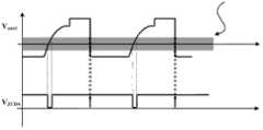
图2绘示图1中的无桥PFC电路工作于电流临界连续模式(CRM)时的电感电流波形、电感峰值电流波形、电感平均电流波形以及开关管的驱动信号的波形示意图;FIG. 2 shows a schematic diagram of the inductor current waveform, the inductor peak current waveform, the inductor average current waveform, and the driving signal of the switching tube when the bridgeless PFC circuit in FIG. 1 works in the current critical continuous mode (CRM);
图3(a)绘示图1中的交流输入电压为正向电压时,第二开关管导通时的电流路径示意图,图3(b)绘示图1中的交流输入电压为正向电压时,第二开关管关断并通过第一开关管的体二极管进行续流时的电流路径示意图;Figure 3(a) shows a schematic diagram of the current path when the second switch is turned on when the AC input voltage in Figure 1 is a forward voltage, and Figure 3(b) shows that the AC input voltage in Figure 1 is a forward voltage , the schematic diagram of the current path when the second switching tube is turned off and freewheeling through the body diode of the first switching tube;
图3(c)绘示图1中的交流输入电压为负向电压时,第一开关管导通时的电流路径示意图,图3(d)绘示图1中的交流输入电压为负向电压时,第一开关管关断并通过第二开关管的体二极管进行续流时的电流路径示意图;Figure 3(c) shows a schematic diagram of the current path when the first switch is turned on when the AC input voltage in Figure 1 is a negative voltage, and Figure 3(d) shows that the AC input voltage in Figure 1 is a negative voltage , the schematic diagram of the current path when the first switching tube is turned off and freewheeling through the body diode of the second switching tube;
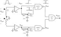
图4绘示依据本发明的一实施方式,用于PFC电路的控制电路的结构框图;FIG. 4 shows a structural block diagram of a control circuit for a PFC circuit according to an embodiment of the present invention;
图5绘示图4的控制电路中的信号转换电路的第一实施例;FIG. 5 illustrates a first embodiment of the signal conversion circuit in the control circuit of FIG. 4;
图6绘示图5的信号转换电路所输出的电流过零检测信号的波形示意图;FIG. 6 is a schematic waveform diagram of a current zero-crossing detection signal output by the signal conversion circuit in FIG. 5;
图7绘示图4的控制电路中的信号转换电路的第二实施例;FIG. 7 illustrates a second embodiment of the signal conversion circuit in the control circuit of FIG. 4;
图8绘示图7的信号转换电路所输出的电流过零检测信号的波形示意图;FIG. 8 is a schematic waveform diagram of a current zero-crossing detection signal output by the signal conversion circuit in FIG. 7;
图9绘示图4的控制电路中的信号转换电路的第三实施例;FIG. 9 illustrates a third embodiment of the signal conversion circuit in the control circuit of FIG. 4;
图10绘示图9的信号转换电路所输出的电流过零检测信号的波形示意图;FIG. 10 is a schematic waveform diagram of a current zero-crossing detection signal output by the signal conversion circuit of FIG. 9;
图11绘示依据本发明的另一实施方式,用于PFC电路的控制电路的结构框图;FIG. 11 shows a structural block diagram of a control circuit for a PFC circuit according to another embodiment of the present invention;
图12绘示图11的控制电路中的边沿检测电路的第一实施例;FIG. 12 illustrates a first embodiment of the edge detection circuit in the control circuit of FIG. 11;
图13绘示图12的边沿检测电路所输出的电流过零检测信号的波形示意图;FIG. 13 is a schematic waveform diagram of a current zero-crossing detection signal output by the edge detection circuit in FIG. 12;
图14绘示图12的控制电路中的边沿检测电路的第二实施例;FIG. 14 illustrates a second embodiment of the edge detection circuit in the control circuit of FIG. 12;
图15绘示图14的边沿检测电路所输出的电流过零检测信号的波形示意图;FIG. 15 is a schematic waveform diagram of a current zero-crossing detection signal output by the edge detection circuit in FIG. 14;
图16绘示图12的控制电路中的边沿检测电路的第三实施例;FIG. 16 illustrates a third embodiment of the edge detection circuit in the control circuit of FIG. 12;
图17绘示图16的边沿检测电路所输出的电流过零检测信号的波形示意图;FIG. 17 is a schematic waveform diagram of a current zero-crossing detection signal output by the edge detection circuit in FIG. 16;
图18绘示图12的控制电路中的边沿检测电路的第四实施例;以及FIG. 18 illustrates a fourth embodiment of the edge detection circuit in the control circuit of FIG. 12; and
图19绘示图18的边沿检测电路所输出的电流过零检测信号的波形示意图。FIG. 19 is a schematic waveform diagram of a current zero-crossing detection signal output by the edge detection circuit in FIG. 18 .
具体实施方式Detailed ways
为了使本申请所揭示的技术内容更加详尽与完备,可参照附图以及本发明的下述各种具体实施例,附图中相同的标记代表相同或相似的组件。然而,本领域的普通技术人员应当理解,下文中所提供的实施例并非用来限制本发明所涵盖的范围。此外,附图仅仅用于示意性地加以说明,并未依照其原尺寸进行绘制。In order to make the technical content disclosed in this application more detailed and complete, reference may be made to the drawings and the following various specific embodiments of the present invention, and the same symbols in the drawings represent the same or similar components. However, those skilled in the art should understand that the examples provided below are not intended to limit the scope of the present invention. In addition, the drawings are only for schematic illustration and are not drawn according to their original scale.
下面参照附图,对本发明各个方面的具体实施方式作进一步的详细描述。The specific implementation manners of various aspects of the present invention will be further described in detail below with reference to the accompanying drawings.
于本申请的具体实施方式部分与权利要求书部分,涉及“耦接(coupled with)”之描述,其可泛指一组件透过其他组件而间接连接至另一组件,或是一组件无须透过其他组件而直接连接至另一组件。In the detailed description and claims of this application, the description of "coupled with" can generally refer to a component that is indirectly connected to another component through other components, or a component that does not need to be transparently connected. directly connected to another component through another component.
于本申请的具体实施方式部分与权利要求书部分,除非文中对于冠词有所特别限定,否则“一”与“该”可泛指单个或多个。In the detailed description and claims of this application, unless the article is specifically limited, "a" and "the" can generally refer to a single or a plurality.
本文中所使用的“约”、“大约”或“大致”用以修饰任何可些微变化的数量,但这种些微变化并不会改变其本质。于实施方式中若无特别说明,则代表以“约”、“大约”或“大致”所修饰之数值的误差范围一般是容许在百分之二十以内,较佳地是在百分之十以内,而更佳地则是在百分之五以内。As used herein, "about," "approximately," or "approximately" is used to modify any quantity that may vary slightly, but which does not alter its essence. Unless otherwise specified in the embodiments, it means that the error range of the numerical value modified by "about", "approximately" or "approximately" is generally allowed within 20%, preferably within 10%. Within , and more preferably within 5%.
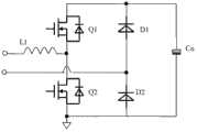
图1绘示无桥PFC电路的电路结构图。参照图1,该无桥PFC(Power Factor Correction,功率因数校正)电路包括第一桥臂和第二桥臂。其中,第一桥臂包括串联连接的一第一开关Q1和一第二开关Q2(如MOSFET),该第一开关Q1与该第二开关Q2的共同节点经由一电感元件L1耦接至一输入电压的一端。第二桥臂包括串联连接的一第三开关和一第四开关,该第三开关与该第四开关的共同节点耦接至该输入电压的另一端。FIG. 1 shows a circuit structure diagram of a bridgeless PFC circuit. Referring to FIG. 1, the bridgeless PFC (Power Factor Correction, power factor correction) circuit includes a first bridge arm and a second bridge arm. Wherein, the first bridge arm includes a first switch Q1 and a second switch Q2 (such as MOSFET) connected in series, and the common node of the first switch Q1 and the second switch Q2 is coupled to an input through an inductance element L1 one end of the voltage. The second bridge arm includes a third switch and a fourth switch connected in series, and a common node of the third switch and the fourth switch is coupled to the other end of the input voltage.
在一实施例中,第三开关和第四开关为慢速恢复二极管,如图1中的D1和D2所示。In one embodiment, the third switch and the fourth switch are slow recovery diodes, as shown by D1 and D2 in FIG. 1 .
在其他的一些实施例中,第一开关Q1和第二开关Q2为快速恢复MOSFET,第三开关和第四开关为慢速恢复MOSFET。例如,快速恢复MOSFET为宽禁带半导体型器件,诸如碳化硅(SiC)或氮化镓(GaN)。In some other embodiments, the first switch Q1 and the second switch Q2 are fast recovery MOSFETs, and the third switch and the fourth switch are slow recovery MOSFETs. For example, fast recovery MOSFETs are wide bandgap semiconductor type devices such as silicon carbide (SiC ) or gallium nitride (GaN ).
图2绘示图1中的无桥PFC电路工作于电流临界连续模式(CRM)时的电感电流波形、电感峰值电流波形、电感平均电流波形以及开关管的驱动信号的波形示意图。2 is a schematic diagram of the inductor current waveform, the inductor peak current waveform, the inductor average current waveform, and the driving signal of the switch tube when the bridgeless PFC circuit in FIG. 1 works in the current critical continuous mode (CRM).
参照图2,无桥PFC电路工作于CRM时,在每一开关周期的结束时刻(或下一开关周期的开始时刻),电感电流刚好下降至零。从图中可以看出,当第一桥臂中的开关管Q1或Q2接收一驱动信号时,自开关管的导通时刻起,电感电流逐渐增大并到达峰值电流(该期间对应于导通时间),然后开关管关断,电感电流从峰值电流逐渐下降至零(该期间对应于关断时间)。由于每一开关周期均包括电感电流的上升期间和下降期间,将上升期间和下降期间的共同点(即峰值电流所对应的点)相连接,即可构成图2中的峰值电流曲线。此外,根据电感电流曲线和峰值电流曲线,也可得到相应的平均电流曲线。Referring to Figure 2, when the bridgeless PFC circuit works in CRM, at the end of each switching cycle (or the beginning of the next switching cycle), the inductor current just drops to zero. It can be seen from the figure that when the switch tube Q1 or Q2 in the first bridge arm receives a driving signal, the inductor current gradually increases and reaches the peak current from the moment the switch tube is turned on (this period corresponds to the turn-on time), and then the switch tube is turned off, and the inductor current gradually decreases from the peak current to zero (this period corresponds to the off time). Since each switching cycle includes a rising period and a falling period of the inductor current, the peak current curve in Figure 2 can be formed by connecting the common points of the rising period and the falling period (that is, the point corresponding to the peak current). In addition, according to the inductor current curve and the peak current curve, the corresponding average current curve can also be obtained.
图3(a)绘示图1中的交流输入电压为正向电压时,第二开关管导通时的电流路径示意图,图3(b)绘示图1中的交流输入电压为正向电压时,第二开关管关断并通过第一开关管的体二极管进行续流时的电流路径示意图。Figure 3(a) shows a schematic diagram of the current path when the second switch is turned on when the AC input voltage in Figure 1 is a forward voltage, and Figure 3(b) shows that the AC input voltage in Figure 1 is a forward voltage , the schematic diagram of the current path when the second switching tube is turned off and freewheeling through the body diode of the first switching tube.
参照图3(a)和3(b),考虑输入电压为正向电压的情形,若开关管Q2开通,开关管Q1关断时,由电感元件L、开关管Q2和二极管D2形成电流路径。若开关管Q1和Q2均关断时,由电感元件L、开关管Q1的体二极管、电容和二极管D2形成电流路径。Referring to Figures 3(a) and 3(b), consider the case where the input voltage is a forward voltage. If the switch Q2 is turned on and the switch Q1 is turned off, a current path is formed by the inductance element L, the switch Q2 and the diode D2. If both the switching tubes Q1 and Q2 are turned off, a current path is formed by the inductance element L, the body diode of the switching tube Q1, the capacitor and the diode D2.
图3(c)绘示图1中的交流输入电压为负向电压时,第一开关管导通时的电流路径示意图,图3(d)绘示图1中的交流输入电压为负向电压时,第一开关管关断并通过第二开关管的体二极管进行续流时的电流路径示意图Figure 3(c) shows a schematic diagram of the current path when the first switch is turned on when the AC input voltage in Figure 1 is a negative voltage, and Figure 3(d) shows that the AC input voltage in Figure 1 is a negative voltage Schematic diagram of the current path when the first switching tube is turned off and freewheeling through the body diode of the second switching tube
参照图3(c)和3(d),考虑输入电压为负向电压的情形,若开关管Q1开通,开关管Q2关断时,由二极管D 1、开关管Q1和电感元件L形成电流路径。若开关管Q1和Q2均关断时,由二极管D1、电容、开关管Q2的体二极管和电感元件L形成电流路径。Referring to Figures 3(c) and 3(d), consider the case where the input voltage is a negative voltage. If the switch tube Q1 is turned on and the switch tube Q2 is turned off, the current path is formed by the diode D1, the switch tube Q1 and the inductance element L . If both the switch tubes Q1 and Q2 are turned off, a current path is formed by the diode D1, the capacitor, the body diode of the switch tube Q2 and the inductance element L.
图4绘示依据本发明的一实施方式,用于PFC电路的控制电路的结构框图。FIG. 4 is a structural block diagram of a control circuit for a PFC circuit according to an embodiment of the present invention.
参照图4,本发明用于无桥PFC电路的控制电路包括一零电流检测电路、一反馈电路和一脉冲分配电路。Referring to FIG. 4 , the control circuit used in the bridgeless PFC circuit of the present invention includes a zero current detection circuit, a feedback circuit and a pulse distribution circuit.
该零电流检测电路包括一极性检测电路和一信号转换电路。该极性检测电路接收交流电源的输入电压,并输出能够表征输入电压极性的一第一数字信号和一第二数字信号。在此,第一数字信号和第二数字信号的电平极性始终相反,当第一数字信号为高电平时,第二数字信号为低电平;当第一数字信号为低电平时,第二数字信号为高电平。该信号转换电路接收用以反映电感元件L1的感应电压的至少一感应信号以及上述第一和第二数字信号,并产生一模拟信号。The zero current detection circuit includes a polarity detection circuit and a signal conversion circuit. The polarity detection circuit receives the input voltage of the AC power supply, and outputs a first digital signal and a second digital signal which can represent the polarity of the input voltage. Here, the level polarities of the first digital signal and the second digital signal are always opposite. When the first digital signal is at a high level, the second digital signal is at a low level; when the first digital signal is at a low level, the second digital signal is at a low level. The second digital signal is at high level. The signal conversion circuit receives at least one induction signal for reflecting the induction voltage of the inductance element L1 and the above-mentioned first and second digital signals, and generates an analog signal.
应当理解,该控制电路既可通过两个辅助绕组来输出反映电感元件的感应电压的感应信号,也可通过单个辅助绕组来输出反映电感元件的感应电压的感应信号。例如,两个辅助绕组的其中一个辅助绕组用来输出电压极性为正时的感应信号,另一个辅助绕组用来输出电压极性为负时的感应信号。又如,单个辅助绕组的一端用来输出电压极性为正时的感应信号,另一端用来输出电压极性为负时的感应信号。It should be understood that the control circuit can output an induction signal reflecting the induced voltage of the inductive element through two auxiliary windings, or output an induced signal reflecting the induced voltage of the inductive element through a single auxiliary winding. For example, one of the two auxiliary windings is used to output the sensing signal when the voltage polarity is positive, and the other auxiliary winding is used to output the sensing signal when the voltage polarity is negative. For another example, one end of a single auxiliary winding is used to output an induction signal when the voltage polarity is positive, and the other end is used to output an induction signal when the voltage polarity is negative.
反馈电路用来接收来自信号转换电路的模拟信号和一预设脉冲信号,并根据该模拟信号和该预设脉冲信号来产生一驱动脉冲信号。脉冲分配电路电性耦接至极性检测电路和反馈电路,用以根据来自该极性检测电路的第一和第二数字信号,将反馈电路所输出的驱动脉冲信号分配至第一桥臂的第一开关Q1和第二开关Q2,以便第一开关Q1或第二开关Q2执行开通操作。第一开关Q1或第二开关Q2在经历任一开关周期后,当流经电感元件L1的电流下降至一预设阈值时再执行下一开关周期的开通操作,并且第一开关Q1或第二开关Q2在每一开关周期中的开通时间相等。The feedback circuit is used to receive the analog signal and a preset pulse signal from the signal conversion circuit, and generate a driving pulse signal according to the analog signal and the preset pulse signal. The pulse distribution circuit is electrically coupled to the polarity detection circuit and the feedback circuit, and is used for distributing the driving pulse signal output by the feedback circuit to the first bridge arm of the first bridge arm according to the first and second digital signals from the polarity detection circuit. A switch Q1 and a second switch Q2, so that the first switch Q1 or the second switch Q2 performs a turn-on operation. After the first switch Q1 or the second switch Q2 goes through any switching period, when the current flowing through the inductance element L1 drops to a preset threshold, the next switching period is turned on, and the first switch Q1 or the second The on-time of switch Q2 is equal in each switching cycle.
在一实施例中,极性检测电路包括一第一运算放大器100、一第一比较器102和一第一反相器104。In one embodiment, the polarity detection circuit includes a first
第一运算放大器100具有一第一输入端(如正相输入端)、一第二输入端(如负相输入端)和一输出端,其第一输入端和第二输入端分别连接至输入电压的两端,其输出端用以输出反映输入电压极性的一电压信号。第一比较器102具有一第一输入端、一第二输入端和一输出端,其第一输入端耦接至第一运算放大器100的输出端,其第二输入端耦接至一第一参考电压(如接地电压),其输出端用以输出第一数字信号。第一反相器104用以将第一数字信号转换为第二数字信号。因而,极性检测电路输出该第一数字信号和该第二数字信号,且第一和第二数字信号的电平极性始终相反。The first
在一实施例中,反馈电路包括一第二运算放大器200、一第二比较器202和一RS触发器204。In one embodiment, the feedback circuit includes a second
第二运算放大器200具有一第一输入端(如负相输入端)、一第二输入端(如正相输入端)和一输出端,其第一输入端用以接收功率因数控制电路的输出电压(亦即,电容两端的加载电压),其第二输入端耦接至一第二参考电压(如Vref),其输出端输出一差值放大信号。第二比较器202具有一第一输入端、一第二输入端和一输出端,其第一输入端耦接至第二运算放大器200的输出端,其第二输入端用以接收一锯齿波电压信号,其输出端输出预设脉冲信号。RS触发器204具有一预置端S、一复位端R和一输出端Q,其预置端S用以接收来自信号转换电路的模拟信号VZCD,其复位端R用以接收来自第二比较器202的预设脉冲信号,其输出端用以输出该驱动脉冲信号。The second
此外,该反馈电路还包括一延迟电路206,设置于信号转换电路与RS触发器204之间,用以对模拟信号VZCD进行延迟,并将延迟后的模拟信号送至RS触发器204的预置端S。进一步,该反馈电路还包括一比较单元(图中未示),设置于延迟电路206与RS触发器204之间,用以将延迟后的模拟信号转换为相应的数字延迟信号并送至RS触发器204的预置端S。In addition, the feedback circuit also includes a
在一实施例中,该脉冲分配电路包括一第一与门电路300和一第二与门电路302。In one embodiment, the pulse distribution circuit includes a first AND
该第一与门电路300具有一第一输入端、一第二输入端和一输出端,其第一输入端用以接收来自极性检测电路的第一数字信号,其第二输入端用以接收来自反馈电路的驱动脉冲信号,其输出端输出一第一控制信号至第一桥臂的第一开关Q1。The first AND
该第二与门电路302具有一第一输入端、一第二输入端和一输出端,其第一输入端用以接收来自极性检测电路的第二数字信号,其第二输入端用以接收来自反馈电路的驱动脉冲信号,其输出端输出一第二控制信号至第一桥臂的第二开关Q2。由于第二与门电路302所接收的驱动脉冲信号和第一与门电路300所接收的驱动脉冲信号相同,第二数字信号与第一数字信号的电平极性始终相反,因而第一桥臂中的第一开关Q1和第二开关Q2在任意时刻只有一个开关开通,而另一开关处于关断状态。The second AND
例如,当输入电压极性为正时,第一数字信号为低电平且第二数字信号为高电平;当输入电压极性为负时,第一数字信号为高电平且第二数字信号为低电平。For example, when the input voltage polarity is positive, the first digital signal is low level and the second digital signal is high level; when the input voltage polarity is negative, the first digital signal is high level and the second digital signal is high level. signal is low.
本领域的技术人员应当理解,图4不仅可用来描述用于无桥PFC电路的控制电路,而且还可用于描述包含无桥PFC电路和控制电路的电源系统、与该控制电路相对应的控制方法。Those skilled in the art should understand that Fig. 4 can not only be used to describe the control circuit for the bridgeless PFC circuit, but also can be used to describe the power supply system including the bridgeless PFC circuit and the control circuit, and the control method corresponding to the control circuit .
以用于无桥PFC电路的控制方法为例,在该控制方法中,首先,检测输入电压的极性,以输出表征输入电压极性的一第一数字信号和一第二数字信号;然后,根据反映电感元件的感应电压的至少一感应信号、第一数字信号和第二数字信号,经由信号转换处理,产生一模拟信号VZCD;接着,提供一预设脉冲信号,根据模拟信号VZCD和预设脉冲信号,产生一驱动脉冲信号;最后,根据第一数字信号和第二数字信号,将驱动脉冲信号分配至第一开关Q 1与第二开关Q2,以便第一开关Q1和第二开关Q2其中之一执行开通操作。Taking the control method for a bridgeless PFC circuit as an example, in this control method, at first, detect the polarity of the input voltage to output a first digital signal and a second digital signal representing the polarity of the input voltage; then, According to at least one induction signal reflecting the induction voltage of the inductance element, the first digital signal and the second digital signal, through signal conversion processing, an analog signal VZCD is generated; then, a preset pulse signal is provided, according to the analog signal VZCD and Preset the pulse signal to generate a driving pulse signal; finally, according to the first digital signal and the second digital signal, distribute the driving pulse signal to the first switch Q1 and the second switch Q2, so that the first switch Q1 and the second switch One of Q2 performs provisioning operation.
图5绘示图4的控制电路中的信号转换电路的第一实施例。图6绘示图5的信号转换电路所输出的电流过零检测信号的波形示意图。FIG. 5 illustrates a first embodiment of the signal conversion circuit in the control circuit of FIG. 4 . FIG. 6 is a schematic waveform diagram of a current zero-crossing detection signal output by the signal conversion circuit in FIG. 5 .
参照图5,该控制电路包括一第一辅助绕组AUX1和一第二辅助绕组AUX2,均耦合至电感元件L1,第一辅助绕组AUX1产生的一第一感应信号与第二辅助绕组AUX2产生的一第二感应信号的极性相反。Referring to Fig. 5, the control circuit includes a first auxiliary winding AUX1 and a second auxiliary winding AUX2, both of which are coupled to the inductance element L1, a first induction signal generated by the first auxiliary winding AUX1 and a first induction signal generated by the second auxiliary winding AUX2 The polarity of the second sensing signal is opposite.
在一实施例中,信号转换电路包括一第一模拟开关和一第二模拟开关。其中,第一模拟开关由第一电阻R1、第三二极管D3和第一开关管MOS 1构成;第二模拟开关由第二电阻R2、第四二极管D4和第二开关管MOS2构成。In one embodiment, the signal conversion circuit includes a first analog switch and a second analog switch. Wherein, the first analog switch is composed of the first resistor R1, the third diode D3 and the first switch tube MOS1; the second analog switch is composed of the second resistor R2, the fourth diode D4 and the second switch tube MOS2 .
第一电阻R1的一端连接至第一辅助绕组AUX1的第一端。第三二极管D3的阳极连接至第一电阻R1的另一端,阴极连接至信号转换电路的输出端以输出该模拟信号VZCD。第一开关管MOS1的第一端连接至第一电阻R1的另一端以及第三二极管D3的阳极,第二端连接至接地端,控制端用以接收该第二数字信号Vpos。One end of the first resistor R1 is connected to the first end of the first auxiliary winding AUX1. The anode of the third diode D3 is connected to the other end of the first resistor R1, and the cathode is connected to the output end of the signal conversion circuit to output the analog signal VZCD . The first end of the first switch MOS1 is connected to the other end of the first resistor R1 and the anode of the third diode D3, the second end is connected to the ground end, and the control end is used to receive the second digital signal Vpos .
第二电阻R2的一端连接至第二辅助绕组AUX2的第一端。第二辅助绕组AUX2和第一辅助绕组AUX1各自的第二端连接至接地端。第四二极管D4的阳极连接至第二电阻R2的另一端,阴极连接至信号转换电路的输出端以输出该模拟信号VZCD。第二开关管MOS2的第一端连接至第二电阻R2的另一端以及第四二极管D4的阳极,第二开关管MOS2的第二端连接至接地端,第二开关管MOS2的控制端用以接收该第一数字信号Vneg。One end of the second resistor R2 is connected to the first end of the second auxiliary winding AUX2. Second terminals of the second auxiliary winding AUX2 and the first auxiliary winding AUX1 are connected to the ground. The anode of the fourth diode D4 is connected to the other end of the second resistor R2, and the cathode is connected to the output end of the signal conversion circuit to output the analog signal VZCD . The first end of the second switching tube MOS2 is connected to the other end of the second resistor R2 and the anode of the fourth diode D4, the second end of the second switching tube MOS2 is connected to the ground terminal, and the control terminal of the second switching tube MOS2 for receiving the first digital signal Vneg .
由图6可知,在输入电压的周期内,第一辅助绕组两端的电压VAUX1与第二辅助绕组两端的电压VAUX2的电压波形始终相反。而第一模拟开关中的电阻R1与二极管D3的共同节点处的电位Va与第二模拟开关中的电阻R2与二极管D4的共同节点处的电位Vb在输入电压的前半周期和后半周期的波形刚好相反。例如,在输入电压的前半周期,电位Va为低电平,电位Vb跟随第二辅助绕组的电压波形变化,对应地,信号转换电路所输出的模拟信号VZCD与电位Vb的波形相同。又如,在输入电压的后半周期,电位Vb为低电平,电位Va跟随第一辅助绕组的电压波形变化,对应地,信号转换电路所输出的模拟信号VZCD与电位Va的波形相同。It can be seen from FIG. 6 that, within a cycle of the input voltage, the voltage waveforms of the voltage VAUX1 across the first auxiliary winding and the voltage VAUX2 across the second auxiliary winding are always opposite. The waveforms of the potential Va at the common node of the resistor R1 and the diode D3 in the first analog switch and the potential Vb at the common node of the resistor R2 and the diode D4 in the second analog switch in the first half cycle and the second half cycle of the input voltage Just the opposite. For example, in the first half period of the input voltage, the potential Va is at a low level, and the potential Vb follows the voltage waveform of the second auxiliary winding. Correspondingly, the analog signal VZCD output by the signal conversion circuit has the same waveform as the potential Vb. For another example, in the second half cycle of the input voltage, the potential Vb is at low level, and the potential Va follows the voltage waveform of the first auxiliary winding. Correspondingly, the analog signal VZCD output by the signal conversion circuit has the same waveform as the potential Va.
此外,模拟信号VZCD的波形中,t1~t2期间表示电感电流从正向峰值下降到零的阶段,t2~t3期间表示电感电流从零到负向峰值的阶段,t3~t4期间表示电感电流从负向峰值恢复至零电流的阶段。类似地,t5~t6期间表示电感电流从负向峰值至零电流的阶段,t6~t7期间表示电感电流从零到正向峰值的阶段,t7~t8期间表示电感电流从正向峰值下降到零的阶段。In addition, in the waveform of the analog signal VZCD , the period from t1 to t2 represents the stage when the inductor current drops from the positive peak to zero, the period from t2 to t3 represents the stage when the inductor current goes from zero to the negative peak value, and the period from t3 to t4 represents the stage when the inductor current The phase of recovery from negative going peak to zero current. Similarly, the period from t5 to t6 represents the stage when the inductor current goes from negative peak to zero current, the period from t6 to t7 represents the stage when the inductor current goes from zero to the positive peak, and the period from t7 to t8 represents the period when the inductor current drops from the positive peak to zero stage.
图7绘示图4的控制电路中的信号转换电路的第二实施例。图8绘示图7的信号转换电路所输出的电流过零检测信号的波形示意图。FIG. 7 illustrates a second embodiment of the signal conversion circuit in the control circuit of FIG. 4 . FIG. 8 is a schematic waveform diagram of a current zero-crossing detection signal output by the signal conversion circuit in FIG. 7 .
参照图7,该控制电路包括一第一辅助绕组AUX1和一第二辅助绕组AUX2,均耦合至电感元件L1,第一辅助绕组AUX1产生的一第一感应信号与第二辅助绕组AUX2产生的一第二感应信号的极性相反。Referring to Fig. 7, the control circuit includes a first auxiliary winding AUX1 and a second auxiliary winding AUX2, both of which are coupled to the inductance element L1, a first induction signal generated by the first auxiliary winding AUX1 and a first induction signal generated by the second auxiliary winding AUX2 The polarity of the second sensing signal is opposite.
在一实施例中,信号转换电路包括一第一模拟开关和一第二模拟开关。其中,第一模拟开关由第五电阻R5、第三开关管MOS3和第五开关管MOS5构成;第二模拟开关由第六电阻R6、第四开关管MOS4和第六开关管MOS6构成。In one embodiment, the signal conversion circuit includes a first analog switch and a second analog switch. Wherein, the first analog switch is composed of the fifth resistor R5, the third switching tube MOS3 and the fifth switching tube MOS5; the second analog switch is composed of the sixth resistor R6, the fourth switching tube MOS4 and the sixth switching tube MOS6.
第五电阻R5的一端连接至第一辅助绕组AUX1的第一端。第三开关管MOS3的第一端连接至第一辅助绕组AUX1的第一端,其第二端连接至一第七二极管D7的阳极,其控制端连接至第五电阻R5的另一端。第五开关管MOS5的第一端连接至第五电阻R5的另一端和第三开关管MOS3的控制端,其第二端连接至接地端,其控制端用以接收第一数字信号Vneg。One end of the fifth resistor R5 is connected to the first end of the first auxiliary winding AUX1. A first end of the third switching transistor MOS3 is connected to the first end of the first auxiliary winding AUX1, a second end thereof is connected to the anode of a seventh diode D7, and a control end thereof is connected to the other end of the fifth resistor R5. The first end of the fifth switch MOS5 is connected to the other end of the fifth resistor R5 and the control end of the third switch MOS3 , the second end is connected to the ground, and the control end is used to receive the first digital signal Vneg .
第六电阻R6的一端连接至第二辅助绕组AUX2的第一端。第二辅助绕组AUX2和第一辅助绕组AUX1各自的第二端连接至接地端。第四开关管MOS4的第一端连接至第二辅助绕组AUX2的第一端,其第二端连接至一第八二极管D8的阳极,其控制端连接至第六电阻R6的另一端。第六开关管MOS6的第一端连接至第六电阻R6的另一端和第四开关管MOS4的控制端,其第二端连接至接地端,其控制端用以接收第二数字信号Vpos,第七二极管D7与第八二极管D8各自的阴极连接至信号转换电路的输出端以输出模拟信号VZCD。One end of the sixth resistor R6 is connected to the first end of the second auxiliary winding AUX2. Second terminals of the second auxiliary winding AUX2 and the first auxiliary winding AUX1 are connected to the ground. The first end of the fourth switching tube MOS4 is connected to the first end of the second auxiliary winding AUX2, the second end is connected to the anode of an eighth diode D8, and the control end is connected to the other end of the sixth resistor R6. The first terminal of the sixth switching tube MOS6 is connected to the other end of the sixth resistor R6 and the control terminal of the fourth switching tube MOS4, the second terminal thereof is connected to the ground terminal, and the control terminal thereof is used to receive the second digital signal Vpos , Respective cathodes of the seventh diode D7 and the eighth diode D8 are connected to the output terminal of the signal conversion circuit to output the analog signal VZCD .
图8中的第一辅助绕组AUX1、第二辅助绕组AUX2和模拟信号VZCD的各自波形与图6相同或相似,为描述简便起见,此处不再赘述。The respective waveforms of the first auxiliary winding AUX1 , the second auxiliary winding AUX2 and the analog signal VZCD in FIG. 8 are the same or similar to those in FIG. 6 , and will not be repeated here for the sake of simplicity.
图9绘示图4的控制电路中的信号转换电路的第三实施例。图10绘示图9的信号转换电路所输出的电流过零检测信号的波形示意图。FIG. 9 illustrates a third embodiment of the signal conversion circuit in the control circuit of FIG. 4 . FIG. 10 is a schematic waveform diagram of a current zero-crossing detection signal output by the signal conversion circuit in FIG. 9 .
参照图9,该控制电路包括单个辅助绕组AUX1,耦合至电感元件L1,藉由该辅助绕组AUX1所产生的一第三感应信号、第一数字信号和第二数字信号来产生模拟信号VZCD。Referring to FIG. 9 , the control circuit includes a single auxiliary winding AUX1 coupled to the inductance element L1 , and an analog signal VZCD is generated by a third induction signal, the first digital signal and the second digital signal generated by the auxiliary winding AUX1 .
在一实施例中,信号转换电路包括一第一模拟开关和一第二模拟开关。其中,第一模拟开关由第七电阻R7、第九二极管D9和第七开关管MOS7构成;第二模拟开关由第八电阻R8、第十二极管D10和第八开关管MOS8构成。In one embodiment, the signal conversion circuit includes a first analog switch and a second analog switch. Wherein, the first analog switch is composed of the seventh resistor R7, the ninth diode D9 and the seventh switching tube MOS7; the second analog switch is composed of the eighth resistor R8, the tenth diode D10 and the eighth switching tube MOS8.
第七电阻R7的一端连接至辅助绕组AUX1的第一端。第九二极管D9的阳极连接至第七电阻R7的另一端,其阴极连接至信号转换电路的输出端以输出模拟信号VZCD。第七开关管MOS7的第一端连接至第七电阻R7的另一端以及第九二极管D9的阳极,其第二端连接至接地端,其控制端用以接收第二数字信号Vpos。One end of the seventh resistor R7 is connected to the first end of the auxiliary winding AUX1. The anode of the ninth diode D9 is connected to the other end of the seventh resistor R7, and the cathode thereof is connected to the output end of the signal conversion circuit to output the analog signal VZCD . A first end of the seventh switching transistor MOS7 is connected to the other end of the seventh resistor R7 and the anode of the ninth diode D9 , its second end is connected to the ground end, and its control end is used to receive the second digital signal Vpos .
第八电阻R8的一端连接至辅助绕组AUX1的第二端。第十二极管D10的阳极连接至第八电阻R8的另一端,阴极连接至信号转换电路的输出端以输出该模拟信号VZCD。第八开关管MOS8的第一端连接至第八电阻R8的另一端以及第十二极管D10的阳极,其第二端连接至接地端,其控制端用以接收第一数字信号Vneg。One end of the eighth resistor R8 is connected to the second end of the auxiliary winding AUX1. The anode of the tenth diode D10 is connected to the other end of the eighth resistor R8, and the cathode is connected to the output end of the signal conversion circuit to output the analog signal VZCD . A first end of the eighth switching transistor MOS8 is connected to the other end of the eighth resistor R8 and an anode of the tenth diode D10 , a second end thereof is connected to the ground end, and a control end thereof is used for receiving the first digital signal Vneg .
结合图9和图10,当输入电压位于前半周期时,第一数字信号Vneg为低电平,第二数字信号Vpos为高电平,此时第七开关管MOS7开通,第八开关管MOS8关断,因而,Va3的电位持续为接地电压,此时Vb3的电位跟随辅助绕组AUX1的负极端子的电压波形变化(与辅助绕组电压波形VAUX1的变化趋势相反)。类似地,当输入电压位于后半周期时,第一数字信号Vneg为高电平,第二数字信号Vpos为低电平,此时第七开关管MOS7关断,第八开关管MOS8开通,因而,Vb3的电位持续为接地电压,此时Va3的电位跟随辅助绕组AUX1的正极端子的电压波形变化(与辅助绕组电压波形VAUX1的变化趋势相同)。9 and 10, when the input voltage is in the first half cycle, the first digital signal Vneg is low level, the second digital signal Vpos is high level, at this time the seventh switching tube MOS7 is turned on, and the eighth switching tube MOS8 is turned off, so the potential of Va3 continues to be the ground voltage, and the potential of Vb3 follows the voltage waveform of the negative terminal of the auxiliary winding AUX1 (opposite to the changing trend of the auxiliary winding voltage waveform VAUX1 ). Similarly, when the input voltage is in the second half cycle, the first digital signal Vneg is at high level, and the second digital signal Vpos is at low level, at this time the seventh switching tube MOS7 is turned off, and the eighth switching tube MOS8 is turned on , Therefore, the potential of Vb3 remains at the ground voltage, and the potential of Va3 follows the voltage waveform of the positive terminal of the auxiliary winding AUX1 (the same trend as the voltage waveform VAUX1 of the auxiliary winding).
图11绘示依据本发明的另一实施方式,用于PFC电路的控制电路的结构框图。FIG. 11 is a structural block diagram of a control circuit for a PFC circuit according to another embodiment of the present invention.
参照图11,本发明用于无桥PFC电路的控制电路包括一零电流检测电路、一反馈电路和一脉冲分配电路。Referring to FIG. 11 , the control circuit used in the bridgeless PFC circuit of the present invention includes a zero current detection circuit, a feedback circuit and a pulse distribution circuit.
该零电流检测电路包括一边沿检测电路406和一使能电路。该边沿检测电路406接收反映电感元件L1的感应电压的至少一感应信号,检测并输出该感应信号中的上升沿或下降沿。该使能电路对所检测的上升沿或下降沿进行过滤,输出一零电流检测信号VZCD。The zero current detection circuit includes an
反馈电路用以接收该零电流检测信号VZCD和一预设脉冲信号,并根据该模拟信号和该预设脉冲信号来产生一驱动脉冲信号。脉冲分配电路包括一极性检测电路,该极性检测电路接收输入电压,并输出用以表征输入电压极性的一第一数字信号和一第二数字信号,第一数字信号和第二数字信号的电平相反。该脉冲分配电路根据第一和第二数字信号将所接收的驱动脉冲信号分配至第一桥臂的第一开关Q 1和第二开关Q2,以便第一开关Q1或第二开关Q2执行开通操作,第一开关Q1或第二开关Q2在经历任一开关周期后,当流经电感元件L1的电流下降至一预设阈值时再执行下一开关周期的开通操作,并且第一开关Q1或第二开关Q2在每一开关周期中的开通时间相等。The feedback circuit is used for receiving the zero current detection signal VZCD and a preset pulse signal, and generating a driving pulse signal according to the analog signal and the preset pulse signal. The pulse distribution circuit includes a polarity detection circuit, the polarity detection circuit receives the input voltage, and outputs a first digital signal and a second digital signal used to characterize the polarity of the input voltage, the first digital signal and the second digital signal level is opposite. The pulse distribution circuit distributes the received drive pulse signal to the first switch Q1 and the second switch Q2 of the first bridge arm according to the first and second digital signals, so that the first switch Q1 or the second switch Q2 performs the turn-on operation After the first switch Q1 or the second switch Q2 goes through any switching period, when the current flowing through the inductance element L1 drops to a preset threshold value, the turn-on operation of the next switching period is performed, and the first switch Q1 or the second switch The turn-on time of the two switches Q2 in each switching cycle is equal.
将图11与图4进行比较,其主要的区别是在于,图11中的极性检测电路不再检测电感电流波形的过零点,而是用于将驱动脉冲信号分配给开关管Q1或Q2。亦即,图11的极性检测电路所输出的、用以表征输入电压极性的第一和第二数字信号作用于驱动脉冲信号,以控制开关管Q1开通或开关管Q2开通。相比之下,图4的极性检测电路需要将第一和第二数字信号送入信号转换电路,以便信号转换电路利用该第一和第二数字信号以及感应信号来输出模拟信号VZCD,即,用于零电流检测(ZCD,Zero CurrentDetection)的模拟信号。Comparing Figure 11 with Figure 4, the main difference is that the polarity detection circuit in Figure 11 no longer detects the zero-crossing point of the inductor current waveform, but is used to distribute the driving pulse signal to the switch tube Q1 or Q2. That is, the first and second digital signals output by the polarity detection circuit in FIG. 11 and used to characterize the polarity of the input voltage act on the driving pulse signal to control the switch Q1 or the switch Q2 to be turned on. In contrast, the polarity detection circuit in FIG. 4 needs to send the first and second digital signals into the signal conversion circuit, so that the signal conversion circuit uses the first and second digital signals and the sensing signal to output an analog signal VZCD , That is, an analog signal for Zero Current Detection (ZCD, Zero Current Detection).
在一实施例中,极性检测电路包括一第一运算放大器604、一第一比较器606和一第一反相器608。其中,第一运算放大器604、第一比较器606和第一反相器608分别与图4中的第一运算放大器100、第一比较器102和第一反相器104的连接方式相同或相似,为描述方便起见,此处不再赘述。In one embodiment, the polarity detection circuit includes a first
在一实施例中,反馈电路包括一第二运算放大器500、一第二比较器502和一RS触发器504。其中,第二运算放大器500、第二比较器502和RS触发器504分别与图4中的第二运算放大器200、第二比较器202和RS触发器204的连接方式相同或相似,为描述方便起见,此处不再赘述。In one embodiment, the feedback circuit includes a second
此外,零电流检测电路还包括一延迟电路408,设置于使能电路与RS触发器504之间,用以对零电流检测信号VZCD进行延迟,并将延迟后的零电流检测信号送至RS触发器504的预置端S。如图11所示,使能电路由开关管MOS1、电阻R1和电容C2构成,用于选择正确的边沿信号,避免产生错误的电流过零检测信号,下文中将结合图12和图13进一步加以说明。In addition, the zero current detection circuit also includes a
在一实施例中,零电流检测电路还包括一比较单元(图中未示),设置于延迟电路408与RS触发器504之间,用以将延迟后的零电流检测信号转换为相应的数字延迟信号并送至RS触发器504的预置端S。In one embodiment, the zero current detection circuit further includes a comparison unit (not shown in the figure), which is arranged between the
在一实施例中,该脉冲分配电路包括一第一与门电路600和一第二与门电路602。In one embodiment, the pulse distribution circuit includes a first AND
该第一与门电路600具有一第一输入端、一第二输入端和一输出端,其第一输入端用以接收来自极性检测电路的第一数字信号,其第二输入端用以接收来自反馈电路的驱动脉冲信号,其输出端输出一第一控制信号至第一桥臂的第一开关Q1。The first AND
该第二与门电路602具有一第一输入端、一第二输入端和一输出端,其第一输入端用以接收来自极性检测电路的第二数字信号,其第二输入端用以接收来自反馈电路的驱动脉冲信号,其输出端输出一第二控制信号至第一桥臂的第二开关Q2。由于第二与门电路602所接收的驱动脉冲信号和第一与门电路600所接收的驱动脉冲信号相同,第二数字信号与第一数字信号的电平极性始终相反,因而第一桥臂中的第一开关Q1和第二开关Q2在任意时刻只有一个开关开通,而另一开关处于关断状态。The second AND
例如,当输入电压极性为正时,第一数字信号为低电平且第二数字信号为高电平;当输入电压极性为负时,第一数字信号为高电平且第二数字信号为低电平。For example, when the input voltage polarity is positive, the first digital signal is low level and the second digital signal is high level; when the input voltage polarity is negative, the first digital signal is high level and the second digital signal is high level. signal is low.
在一实施例中,该使能电路包括开关管MOS1、电阻R1和电容C2。具体地,开关管MOS1的第一端电性连接至电阻R1的第一端,开关管MOS1的第二端连接至边沿检测电路406的输出端,开关管MOS1的第三端连接至接地电压。电阻R1的第一端电性连接至开关管MOS1的第一端,电阻R1的第二端电性连接至反馈电路的输出端。电容C2的一端连接至开关管MOS1的第一端和电阻R1的第一端,电容C2的另一端连接至开关管MOS1的第三端。该使能电路根据反馈电路输出的驱动脉冲信号对边沿检测电路406所输出的感应信号中的上升沿或下降沿进行过滤,从而提取正确的边沿信号。In one embodiment, the enabling circuit includes a switch MOS1, a resistor R1 and a capacitor C2. Specifically, the first terminal of the switch MOS1 is electrically connected to the first terminal of the resistor R1, the second terminal of the switch MOS1 is connected to the output terminal of the
本领域的技术人员应当理解,图11不仅可用来描述用于无桥PFC电路的控制电路,而且还可用于描述包含无桥PFC电路和控制电路的电源系统、与该控制电路相对应的控制方法。Those skilled in the art should understand that Fig. 11 can not only be used to describe the control circuit for the bridgeless PFC circuit, but also can be used to describe the power supply system including the bridgeless PFC circuit and the control circuit, and the control method corresponding to the control circuit .
以用于无桥PFC电路的控制方法为例,在该控制方法中,首先,接收用以反映电感元件的感应电压的至少一感应信号,经由边沿检测和过滤处理,产生一零电流检测信号;然后,提供一预设脉冲信号,根据零电流检测信号和预设脉冲信号,产生一驱动脉冲信号;接着,检测输入电压的极性,以输出表征输入电压极性的一第一数字信号和一第二数字信号;最后,根据第一数字信号和第二数字信号,将驱动脉冲信号分配至第一开关Q1与第二开关Q2,以便第一开关Q1和第二开关Q2其中之一执行开通操作。Taking the control method for a bridgeless PFC circuit as an example, in the control method, first, at least one induction signal for reflecting the induction voltage of the inductance element is received, and a zero current detection signal is generated through edge detection and filtering processing; Then, a preset pulse signal is provided, and a driving pulse signal is generated according to the zero current detection signal and the preset pulse signal; then, the polarity of the input voltage is detected to output a first digital signal representing the polarity of the input voltage and a The second digital signal; finally, according to the first digital signal and the second digital signal, the driving pulse signal is distributed to the first switch Q1 and the second switch Q2, so that one of the first switch Q1 and the second switch Q2 performs an opening operation .
图12绘示图11的控制电路中的边沿检测电路的第一实施例。图13绘示图12的边沿检测电路所输出的电流过零检测信号的波形示意图。FIG. 12 illustrates a first embodiment of the edge detection circuit in the control circuit of FIG. 11 . FIG. 13 is a schematic waveform diagram of a current zero-crossing detection signal output by the edge detection circuit in FIG. 12 .
参照图12,该控制电路包括一第一辅助绕组AUX1和一第二辅助绕组AUX2,均耦合至电感元件L1,第一辅助绕组AUX1产生的一第一感应信号与第二辅助绕组AUX2产生的一第二感应信号的极性相反。Referring to Fig. 12, the control circuit includes a first auxiliary winding AUX1 and a second auxiliary winding AUX2, both of which are coupled to the inductance element L1, a first induction signal generated by the first auxiliary winding AUX1 and a first induction signal generated by the second auxiliary winding AUX2 The polarity of the second sensing signal is opposite.
在一实施例中,边沿检测电路包括一第一模拟开关和一第二模拟开关。其中,第一模拟开关由第三电阻R3、第五二极管D5和第三电容C3构成;第二模拟开关由第四电阻R4、第六二极管D6和第四电容C4构成。In one embodiment, the edge detection circuit includes a first analog switch and a second analog switch. Wherein, the first analog switch is composed of the third resistor R3, the fifth diode D5 and the third capacitor C3; the second analog switch is composed of the fourth resistor R4, the sixth diode D6 and the fourth capacitor C4.
第三电阻R3的一端连接至第一辅助绕组AUX1的第一端。第五二极管D5的阴极连接至第一辅助绕组AUX1的第一端,阳极连接至第三电阻R3的另一端。第三电容C3的一端连接至第五二极管D5的阳极,另一端连接至接地端。One end of the third resistor R3 is connected to the first end of the first auxiliary winding AUX1. The cathode of the fifth diode D5 is connected to the first end of the first auxiliary winding AUX1, and the anode is connected to the other end of the third resistor R3. One end of the third capacitor C3 is connected to the anode of the fifth diode D5, and the other end is connected to the ground.
第四电阻R4的一端连接至第二辅助绕组AUX2的第一端。第二辅助绕组AUX2和第一辅助绕组AUX1各自的第二端连接至接地端。第六二极管D6的阴极连接至第二辅助绕组AUX2的第一端,阳极连接至第四电阻R4的另一端。第四电容C4的一端连接至第六二极管D6的阳极,另一端连接至接地端,其中,第五二极管D5的阳极和第六二极管D6的阳极还分别连接第三二极管D3和第四二极管D4,藉由第三二极管D3和第四二极管D4输出零电流检测信号VZCD。One end of the fourth resistor R4 is connected to the first end of the second auxiliary winding AUX2. Second terminals of the second auxiliary winding AUX2 and the first auxiliary winding AUX1 are connected to the ground. The cathode of the sixth diode D6 is connected to the first end of the second auxiliary winding AUX2, and the anode is connected to the other end of the fourth resistor R4. One end of the fourth capacitor C4 is connected to the anode of the sixth diode D6, and the other end is connected to the ground, wherein, the anode of the fifth diode D5 and the anode of the sixth diode D6 are respectively connected to the third diode The transistor D3 and the fourth diode D4 output a zero current detection signal VZCD through the third diode D3 and the fourth diode D4.
结合图12和图13,在t1时刻,电容C3上的电压VC3从正压信号变成负压信号,存在一个下降沿。如果未设置上述使能电路,经过二极管D3和D4所组成的逻辑与电路后,VZCD在t1时刻将同时产生一对应的下降沿波形。然而,该下降沿是因为开关管动作导致辅助绕组两端电压的反转,并非正确的边沿信号。因而,藉由使能电路来接收开关管的驱动信号VDRV,经过电阻R1和C2后产生一定的延时,以驱动开关管MOS1从而使VZCD在VDRV为正的时间段内是一个低电平信号,如图13中的VTH。这样,通过VZCD和使能电路就过滤了错误的跳变信号,得到正确的零电流检测信号。Referring to FIG. 12 and FIG. 13 , at time t1 , the voltage VC3 on capacitor C3 changes from a positive voltage signal to a negative voltage signal, and there is a falling edge. If the above-mentioned enabling circuit is not set, VZCD will generate a corresponding falling edge waveform at the time t1 after passing through the logical AND circuit formed by the diodes D3 and D4. However, the falling edge is not a correct edge signal because of the reversal of the voltage across the auxiliary winding due to the action of the switching tube. Therefore, the drive signal VDRV of the switch tube is received by the enabling circuit, and a certain delay is generated after passing through the resistors R1 and C2 to drive the switch tube MOS1 so that VZCD is a low during the period when VDRV is positive. Level signal, such as VTH in Figure 13. In this way, the wrong jump signal is filtered through VZCD and the enable circuit, and the correct zero current detection signal is obtained.
图14绘示图12的控制电路中的边沿检测电路的第二实施例。图15绘示图14的边沿检测电路所输出的电流过零检测信号的波形示意图。FIG. 14 illustrates a second embodiment of the edge detection circuit in the control circuit of FIG. 12 . FIG. 15 is a schematic waveform diagram of a current zero-crossing detection signal output by the edge detection circuit in FIG. 14 .
参照图14,该边沿检测电路包括一第一检测模组和一第二检测模组。其中,该第一检测模组由一第一运算放大器A2-1、一RC电路、一反相器N2-1和一与非门电路2-1构成;该第二检测模组由一第二运算放大器A2-2、一RC电路、一反相器N2-2和一与非门电路2-2构成。Referring to FIG. 14 , the edge detection circuit includes a first detection module and a second detection module. Wherein, the first detection module is composed of a first operational amplifier A2-1, an RC circuit, an inverter N2-1 and a NAND gate circuit 2-1; the second detection module is composed of a second Operational amplifier A2-2, an RC circuit, an inverter N2-2 and a NAND gate circuit 2-2 constitute.
第一运算放大器A2-1具有一第一输入端、一第二输入端和一输出端,其第一输入端连接至第一辅助绕组AUX1的第一端,其第二输入端连接至一接地电压,其输出端输出一第一数字信号VD2-1。RC电路具有一第一电阻R2-1和一第一电容C2-1,第一电阻R2-1的一端连接至第一运算放大器A2-1的输出端,第一电容C2-1的一端连接至接地端。反相器N2-1的输入端连接至第一电阻R2-1和第一电容C2-1的共同节点。与非门电路2-1具有一第一输入端、一第二输入端和一输出端,其第一输入端连接至第一运算放大器A2-1的输出端,其第二输入端连接至反相器N2-1的输出端,其输出端输出一第一脉冲信号VD2-3。The first operational amplifier A2-1 has a first input terminal, a second input terminal and an output terminal, its first input terminal is connected to the first terminal of the first auxiliary winding AUX1, and its second input terminal is connected to a ground voltage, and its output terminal outputs a first digital signal VD2-1 . The RC circuit has a first resistor R2-1 and a first capacitor C2-1, one end of the first resistor R2-1 is connected to the output terminal of the first operational amplifier A2-1, and one end of the first capacitor C2-1 is connected to ground terminal. The input terminal of the inverter N2-1 is connected to the common node of the first resistor R2-1 and the first capacitor C2-1. The NAND gate circuit 2-1 has a first input end, a second input end and an output end, and its first input end is connected to the output end of the first operational amplifier A2-1, and its second input end is connected to the inverter The output terminal of the phase switch N2-1 outputs a first pulse signal VD2-3 .
第二运算放大器A2-2具有一第一输入端、一第二输入端和一输出端,其第一输入端连接至第一辅助绕组AUX2的第一端,其第二输入端连接至一接地电压,其输出端输出一第二数字信号VD2-2。RC电路具有一第二电阻R2-2和一第二电容C2-2,第二电阻R2-2的一端连接至第二运算放大器A2-2的输出端,第二电容C2-2的一端连接至接地端。反相器N2-2的输入端连接至第二电阻R2-2和第二电容C2-2的共同节点。与非门电路2-2具有一第一输入端、一第二输入端和一输出端,其第一输入端连接至第二运算放大器A2-2的输出端,其第二输入端连接至反相器N2-2的输出端,其输出端输出一第二脉冲信号VD2-4。其中,第一脉冲信号VD2-3和第二脉冲信号VD2-4进行逻辑与操作,以得到该零电流检测信号。The second operational amplifier A2-2 has a first input terminal, a second input terminal and an output terminal, its first input terminal is connected to the first terminal of the first auxiliary winding AUX2, and its second input terminal is connected to a ground voltage, and its output terminal outputs a second digital signal VD2-2 . The RC circuit has a second resistor R2-2 and a second capacitor C2-2, one end of the second resistor R2-2 is connected to the output terminal of the second operational amplifier A2-2, and one end of the second capacitor C2-2 is connected to ground terminal. The input terminal of the inverter N2-2 is connected to the common node of the second resistor R2-2 and the second capacitor C2-2. The NAND gate circuit 2-2 has a first input end, a second input end and an output end, and its first input end is connected to the output end of the second operational amplifier A2-2, and its second input end is connected to the inverter The output terminal of the phaser N2-2 outputs a second pulse signal VD2-4 . Wherein, the logic AND operation is performed on the first pulse signal VD2-3 and the second pulse signal VD2-4 to obtain the zero current detection signal.
参照图15,第一运算放大器A2-1输出的第一数字信号VD2-1用于对辅助绕组AUX1的电压波形的上升沿进行检测,第二运算放大器A2-2输出的第二数字信号VD2-2用于对辅助绕组AUX2的电压波形的上升沿进行检测,因而该边沿检测电路也可称为上升沿检测电路。此外,零电流检测信号VZCD2为第一脉冲信号VD2-3与第二脉冲信号VD2-4进行逻辑与操作所得到的电压波形。Referring to Fig. 15, the first digital signal VD2-1 output by the first operational amplifier A2-1 is used to detect the rising edge of the voltage waveform of the auxiliary winding AUX1, and the second digital signal V output by the second operational amplifier A2-2D2-2 is used to detect the rising edge of the voltage waveform of the auxiliary winding AUX2, so this edge detection circuit can also be called a rising edge detection circuit. In addition, the zero current detection signal VZCD2 is a voltage waveform obtained by logical AND operation of the first pulse signal VD2 - 3 and the second pulse signal VD2 - 4 .
图16绘示图12的控制电路中的边沿检测电路的第三实施例。图17绘示图16的边沿检测电路所输出的电流过零检测信号的波形示意图。FIG. 16 illustrates a third embodiment of the edge detection circuit in the control circuit of FIG. 12 . FIG. 17 is a schematic waveform diagram of a current zero-crossing detection signal output by the edge detection circuit in FIG. 16 .
参照图16,该控制电路包括单个辅助绕组AUX1,耦合至电感元件L1,藉由辅助绕组AUX1所产生的一第三感应信号来检测并输出第三感应信号中的上升沿或下降沿。Referring to FIG. 16 , the control circuit includes a single auxiliary winding AUX1 coupled to the inductance element L1 to detect and output a rising or falling edge of the third sensing signal through a third sensing signal generated by the auxiliary winding AUX1 .
该边沿检测电路包括一检测模组,该检测模组具有一运算放大器A3-1、一RC电路、一反相器N3-1、一与非门电路3-1和一或门电路3-2构成。The edge detection circuit includes a detection module, the detection module has an operational amplifier A3-1, an RC circuit, an inverter N3-1, a NAND circuit 3-1 and an OR circuit 3-2 constitute.
运算放大器A3-1具有一第一输入端、一第二输入端和一输出端,其第一输入端连接至辅助绕组AUX1的第一端,其第二输入端连接至一接地端,其输出端输出一数字信号VD3-1。RC电路具有一电阻R3-1和一电容C3-1,该电阻R3-1的一端连接至运算放大器A3-1的输出端,该电容C3-1的一端连接至接地端。反相器N3-1的输入端连接至该电阻R3-1和该电容C3-1的共同节点。与非门电路3-1具有一第一输入端、一第二输入端和一输出端,其第一输入端连接至运算放大器A3-1的输出端,其第二输入端连接至反相器N3-1的输出端,其输出端输出一第一脉冲信号VD3-3。或门电路3-2具有一第一输入端、一第二输入端和一输出端,其第一输入端连接至运算放大器A3-1的输出端,其第二输入端连接至反相器N3-1的输出端,其输出端输出一第二脉冲信号VD3-4。第一脉冲信号VD3-3和第二脉冲信号VD3-4进行逻辑与操作,以得到零电流检测信号VZCD3。The operational amplifier A3-1 has a first input terminal, a second input terminal and an output terminal, its first input terminal is connected to the first terminal of the auxiliary winding AUX1, its second input terminal is connected to a ground terminal, and its output Terminal outputs a digital signal VD3-1 . The RC circuit has a resistor R3-1 and a capacitor C3-1, one end of the resistor R3-1 is connected to the output end of the operational amplifier A3-1, and one end of the capacitor C3-1 is connected to the ground. The input terminal of the inverter N3-1 is connected to the common node of the resistor R3-1 and the capacitor C3-1. The NAND gate circuit 3-1 has a first input end, a second input end and an output end, and its first input end is connected to the output end of the operational amplifier A3-1, and its second input end is connected to the inverter The output terminal of N3-1 outputs a first pulse signal VD3-3 . OR gate circuit 3-2 has a first input end, a second input end and an output end, and its first input end is connected to the output end of operational amplifier A3-1, and its second input end is connected to inverter N3 The output terminal of -1 outputs a second pulse signal VD3-4 . A logic AND operation is performed on the first pulse signal VD3 - 3 and the second pulse signal VD3 - 4 to obtain the zero current detection signal VZCD3 .
结合图16和图17,电阻R3-1、电容C3-1、非门N3-1、与非门3-1构成上升沿检测电路,将辅助绕组AUX1的感应电压的上升沿转化为负逻辑的窄脉冲VD3-3。电阻R3-1、电容C3-1、非门N3-1、或门3-2构成下降沿检测电路,将辅助绕组AUX1的感应电压的下降沿转化为负逻辑的窄脉冲VD3-4。与门3-3将上升沿检测电路和下降沿检测电路各自形成的窄脉冲组合在一起,从而产生零电流检测信号VZCD3。因此,该实施例可将辅助绕组的感应电压波形的上升沿和下降沿都转化为负逻辑的窄脉冲,从而实现上升沿检测和下降沿检测的功能。Combining Figure 16 and Figure 17, resistor R3-1, capacitor C3-1, NAND gate N3-1, and NAND gate 3-1 form a rising edge detection circuit, which converts the rising edge of the induced voltage of the auxiliary winding AUX1 into a negative logic narrow pulse VD3-3 . Resistor R3-1, capacitor C3-1, NOT gate N3-1, and OR gate 3-2 constitute a falling edge detection circuit, which converts the falling edge of the induced voltage of the auxiliary winding AUX1 into a negative logic narrow pulse VD3-4 . The AND gate 3-3 combines the respective narrow pulses formed by the rising edge detection circuit and the falling edge detection circuit to generate the zero current detection signal VZCD3 . Therefore, in this embodiment, both the rising edge and the falling edge of the induction voltage waveform of the auxiliary winding can be converted into negative logic narrow pulses, thereby realizing the functions of rising edge detection and falling edge detection.
图18绘示图12的控制电路中的边沿检测电路的第四实施例。图19绘示图18的边沿检测电路所输出的电流过零检测信号的波形示意图。FIG. 18 illustrates a fourth embodiment of the edge detection circuit in the control circuit of FIG. 12 . FIG. 19 is a schematic waveform diagram of a current zero-crossing detection signal output by the edge detection circuit in FIG. 18 .
参照图18,该控制电路包括单个辅助绕组AUX1,耦合至电感元件L1,藉由辅助绕组AUX1所产生的感应信号来检测并输出感应信号中的上升沿或下降沿。Referring to FIG. 18 , the control circuit includes a single auxiliary winding AUX1 coupled to the inductance element L1 to detect and output rising or falling edges of the sensing signal through the sensing signal generated by the auxiliary winding AUX1 .
该边沿检测电路包括一第一光耦合器4-1和一第二光耦合器4-2。第一光耦合器4-1的第一输入端连接至辅助绕组AUX1的第二端,第二输入端经由一第一电阻R4-1连接至辅助绕组AUX1的第一端,第一输出端连接至一电源电压VCC。第二光耦合器4-2的第一输入端连接至第一光耦合器4-1的第二输入端,其第二输入端连接至辅助绕组AUX1的第二端,第一输出端连接至电源电压VCC,其第二输出端连接至第一光耦合器4-1的第二输出端从而输出零电流检测信号VZCD4。The edge detection circuit includes a first optical coupler 4-1 and a second optical coupler 4-2. The first input end of the first optocoupler 4-1 is connected to the second end of the auxiliary winding AUX1, the second input end is connected to the first end of the auxiliary winding AUX1 through a first resistor R4-1, and the first output end is connected to to a supply voltage VCC. The first input end of the second optocoupler 4-2 is connected to the second input end of the first optocoupler 4-1, the second input end thereof is connected to the second end of the auxiliary winding AUX1, and the first output end is connected to The second output terminal of the power supply voltage VCC is connected to the second output terminal of the first optocoupler 4-1 so as to output the zero current detection signal VZCD4 .
结合图18和图19,辅助绕组AUX1的感应电压无跳变时,该感应电压可令光耦合器4-1和4-2中的一个导通,从而使零电流检测信号VZCD4为高电平;当辅助绕组的感应电压反转时(包括感应电压从负压调变为正压以及从正压调变为负压),必然经过光耦合器4-1和4-2共同的截止区,此时,零电流检测信号VZCD4为低电平,从而输出一负逻辑的窄脉冲,同样能够实现辅助绕组的感应电压的边沿检测功能,进而确定电感电流的过零点。18 and 19, when the induction voltage of the auxiliary winding AUX1 has no jump, the induction voltage can make one of the optocouplers 4-1 and 4-2 conduct, so that the zero current detection signal VZCD4 is a high voltage level; when the induction voltage of the auxiliary winding reverses (including the adjustment of the induction voltage from negative voltage to positive voltage and from positive voltage to negative voltage), it must pass through the common cut-off area of optocoupler 4-1 and 4-2 , at this time, the zero-current detection signal VZCD4 is at low level, thereby outputting a narrow pulse of negative logic, which can also realize the edge detection function of the induced voltage of the auxiliary winding, and then determine the zero-crossing point of the inductor current.
上文中,参照附图描述了本发明的具体实施方式。但是,本领域中的普通技术人员能够理解,在不偏离本发明的精神和范围的情况下,还可以对本发明的具体实施方式作各种变更和替换。这些变更和替换都落在本发明权利要求书所限定的范围内。Hereinbefore, specific embodiments of the present invention have been described with reference to the accompanying drawings. However, those skilled in the art can understand that without departing from the spirit and scope of the present invention, various changes and substitutions can be made to the specific embodiments of the present invention. These changes and substitutions all fall within the scope defined by the claims of the present invention.
Claims (64)
Priority Applications (5)
| Application Number | Priority Date | Filing Date | Title |
|---|---|---|---|
| CN201210284439.2ACN102843025B (en) | 2012-08-06 | 2012-08-06 | Control circuit, control method and power supply system for PFC circuit |
| TW104115175ATWI530767B (en) | 2012-08-06 | 2012-11-28 | Control circuit, control method used in pfc circuit and power source system thereof |
| TW101144513ATWI490677B (en) | 2012-08-06 | 2012-11-28 | Control circuit, control method used in pfc circuit and power source system thereof |
| US13/759,043US9189004B2 (en) | 2012-08-06 | 2013-02-05 | Control circuit, control method used in PFC circuit and power source system thereof |
| US14/707,015US9473017B2 (en) | 2012-08-06 | 2015-05-08 | Control circuit, control method used in PFC circuit and power source system thereof |
Applications Claiming Priority (1)
| Application Number | Priority Date | Filing Date | Title |
|---|---|---|---|
| CN201210284439.2ACN102843025B (en) | 2012-08-06 | 2012-08-06 | Control circuit, control method and power supply system for PFC circuit |
Publications (2)
| Publication Number | Publication Date |
|---|---|
| CN102843025Atrue CN102843025A (en) | 2012-12-26 |
| CN102843025B CN102843025B (en) | 2015-01-07 |
Family
ID=47370146
Family Applications (1)
| Application Number | Title | Priority Date | Filing Date |
|---|---|---|---|
| CN201210284439.2AActiveCN102843025B (en) | 2012-08-06 | 2012-08-06 | Control circuit, control method and power supply system for PFC circuit |
Country Status (3)
| Country | Link |
|---|---|
| US (2) | US9189004B2 (en) |
| CN (1) | CN102843025B (en) |
| TW (2) | TWI490677B (en) |
Cited By (19)
| Publication number | Priority date | Publication date | Assignee | Title |
|---|---|---|---|---|
| CN103412181A (en)* | 2013-09-02 | 2013-11-27 | 南京埃科孚电子科技有限公司 | Inductance and current zero-cross detection circuit for correcting boost type power factor |
| CN105004910A (en)* | 2014-04-22 | 2015-10-28 | 中兴通讯股份有限公司 | Current detection method and apparatus of PFC inductor |
| CN105305848A (en)* | 2014-07-22 | 2016-02-03 | 株式会社村田制作所 | Boost inductor demagnetization detection for bridgeless boost pfc converter operating in boundary-conduction mode |
| CN105874694A (en)* | 2013-12-19 | 2016-08-17 | 德克萨斯仪器股份有限公司 | Apparatus and method for zero voltage switching |
| CN106803722A (en)* | 2015-11-26 | 2017-06-06 | 株式会社东芝 | Power inverter |
| CN108649787A (en)* | 2018-06-14 | 2018-10-12 | 广东美的制冷设备有限公司 | Driving circuit, power factor correction controller and driving method |
| CN110445402A (en)* | 2019-07-29 | 2019-11-12 | 深圳市航嘉驰源电气股份有限公司 | Active diode circuit and ac-dc power conversion circuit |
| CN111044772A (en)* | 2019-12-31 | 2020-04-21 | 广州金升阳科技有限公司 | Current sampling circuit and control method |
| CN112165247A (en)* | 2020-09-29 | 2021-01-01 | 广州金升阳科技有限公司 | Zero current sampling method and circuit of bridgeless PFC circuit |
| CN112462127A (en)* | 2019-09-06 | 2021-03-09 | 群光电能科技股份有限公司 | Surge current testing device |
| CN112595885A (en)* | 2020-11-18 | 2021-04-02 | 广州金升阳科技有限公司 | Demagnetization detection circuit and method for PFC circuit system |
| CN113252972A (en)* | 2021-07-02 | 2021-08-13 | 深圳市高斯宝电气技术有限公司 | Bridgeless PFC inductive current zero-crossing detection circuit |
| CN114076844A (en)* | 2020-08-21 | 2022-02-22 | 深圳绿米联创科技有限公司 | Zero-crossing control method, electronic device, and storage medium |
| CN114204797A (en)* | 2021-12-15 | 2022-03-18 | 杭州优特电源有限公司 | Continuous mode bridgeless power factor correction control circuit |
| CN114844343A (en)* | 2022-05-09 | 2022-08-02 | 深圳市科信通信技术股份有限公司 | Soft switch control method, totem-pole bridgeless circuit and system |
| EP3043460B1 (en)* | 2013-10-08 | 2022-10-19 | ZTE Corporation | Control device and method of totem-pole bridgeless pfc soft switch |
| CN115478996A (en)* | 2022-08-31 | 2022-12-16 | 中国大唐集团科学技术研究总院有限公司西北电力试验研究院 | Wind generating set catapulting lightning triggering system |
| CN115622371A (en)* | 2022-10-31 | 2023-01-17 | 深圳市瀚强科技股份有限公司 | Control circuit for bridgeless PFC circuit, control method thereof and power supply system |
| TWI798356B (en)* | 2018-02-16 | 2023-04-11 | 美商微晶片科技公司 | Apparatus and method for performing voltage protection, and microcontroller |
Families Citing this family (21)
| Publication number | Priority date | Publication date | Assignee | Title |
|---|---|---|---|---|
| CN103954828B (en)* | 2014-05-05 | 2017-06-16 | 广东美的暖通设备有限公司 | Voltage detecting circuit and device based on Single-phase PFC |
| CN103995176B (en)* | 2014-05-16 | 2017-05-03 | 南京能瑞自动化设备股份有限公司 | Zero-crossing signal generation method based on coupling coil signals |
| TWI518347B (en)* | 2014-07-28 | 2016-01-21 | 凱立自動化有限公司 | Alternate current detector with automatically judging amount of element under test and monitoring |
| US10390384B2 (en)* | 2015-04-30 | 2019-08-20 | Mediatek Inc. | Apparatuses and methods for reducing circuit switch fallback (CSFB) call setup time |
| TWI605694B (en) | 2016-03-25 | 2017-11-11 | 智原科技股份有限公司 | Receiver loss of signal deglitch apparatus and method |
| CN108964454B (en)* | 2017-05-17 | 2020-07-28 | 中芯国际集成电路制造(上海)有限公司 | DC-DC conversion circuit system and forming method thereof |
| CN109428476B (en)* | 2017-08-30 | 2023-11-10 | 中兴通讯股份有限公司 | An analog control device for a power factor correction circuit |
| US10944337B2 (en) | 2017-12-15 | 2021-03-09 | Texas Instruments Incorporated | Adaptive zero voltage switching (ZVS) loss detection for power converters |
| JP2019176605A (en)* | 2018-03-28 | 2019-10-10 | Tdk株式会社 | Zero current detection circuit for bridgeless totem-pole power factor improving converter, and bridgeless totem-pole power factor improving converter |
| US10461632B1 (en)* | 2018-04-10 | 2019-10-29 | Semiconductor Components Industries, Llc | Current sensing for bridgeless PFC converters |
| US10432086B1 (en)* | 2018-04-10 | 2019-10-01 | Semiconductor Components Industries, Llc | Methods and systems of bridgeless PFC converters |
| US10381915B1 (en)* | 2018-10-04 | 2019-08-13 | Texas Instruments Incorporated | Variable delay for soft switching in power conversion circuit |
| CN111190039B (en)* | 2018-11-14 | 2022-06-28 | 台达电子工业股份有限公司 | Current detection circuit of power converter |
| CN111446860B (en)* | 2019-01-16 | 2021-09-21 | 台达电子企业管理(上海)有限公司 | DC/DC converter and control method thereof |
| CN111446861B (en) | 2019-01-16 | 2021-02-26 | 台达电子企业管理(上海)有限公司 | DC/DC converter and control method thereof |
| CN112003454B (en)* | 2019-05-27 | 2025-06-13 | 恩智浦美国有限公司 | Bridgeless power factor correction converter with zero current detection circuit |
| JP7379131B2 (en)* | 2019-12-16 | 2023-11-14 | 東芝テック株式会社 | power converter |
| CN113131734A (en)* | 2019-12-31 | 2021-07-16 | 华为技术有限公司 | Current detection device and power factor correction device |
| CN117652085A (en)* | 2021-09-28 | 2024-03-05 | 华为技术有限公司 | Control method of PFC circuit and PFC circuit |
| CN115085530A (en)* | 2022-07-05 | 2022-09-20 | 华为数字能源技术有限公司 | Noise suppression method, device and electronic device for totem pole PFC circuit |
| CN117254674B (en)* | 2023-11-20 | 2024-02-09 | 珠海镓未来科技有限公司 | PFC drive control module and power factor correction device |
Citations (10)
| Publication number | Priority date | Publication date | Assignee | Title |
|---|---|---|---|---|
| EP2086095A1 (en)* | 2008-10-15 | 2009-08-05 | China Electronics Weihua Co., Ltd. | Phase shift and synchronization control circuit for interleaved PFC controller |
| CN101515726A (en)* | 2009-02-24 | 2009-08-26 | 苏州工业园区华波电子科技有限公司 | High-efficiency high power factor charger circuit |
| CN101860194A (en)* | 2010-05-14 | 2010-10-13 | 北方工业大学 | Implementation method and device of multi-mode power factor corrector |
| CN101951138A (en)* | 2009-07-08 | 2011-01-19 | 三垦电气株式会社 | Power factor correction circuit |
| US20110075462A1 (en)* | 2009-09-30 | 2011-03-31 | Astec International Limited | Bridgeless Boost PFC Circuits and Systems |
| WO2011052197A1 (en)* | 2009-10-29 | 2011-05-05 | Fuji Electric Systems Co., Ltd. | Switching power supply circuit and power factor controller |
| CN102130580A (en)* | 2011-03-30 | 2011-07-20 | 艾默生网络能源系统北美公司 | A Totem Pole Bridgeless Power Factor Correction Circuit |
| CN102340252A (en)* | 2010-07-14 | 2012-02-01 | 东芝泰格有限公司 | power conversion device |
| CN102377354A (en)* | 2010-08-09 | 2012-03-14 | 三垦电气株式会社 | Converter |
| CN102498652A (en)* | 2009-06-30 | 2012-06-13 | 美国思睿逻辑有限公司 | Switching power converter with current sensing transformer auxiliary power supply |
Family Cites Families (7)
| Publication number | Priority date | Publication date | Assignee | Title |
|---|---|---|---|---|
| US6272027B1 (en)* | 2000-07-28 | 2001-08-07 | Simon Fraidlin | AC active clamp for isolated power factor corrector and method of operating the same |
| US7164591B2 (en)* | 2003-10-01 | 2007-01-16 | International Rectifier Corporation | Bridge-less boost (BLB) power factor correction topology controlled with one cycle control |
| JP4715429B2 (en)* | 2005-09-29 | 2011-07-06 | 富士電機システムズ株式会社 | AC / DC converter |
| US7518895B2 (en)* | 2006-06-30 | 2009-04-14 | Fairchild Semiconductor Corporation | High-efficiency power converter system |
| US8199541B2 (en) | 2008-04-11 | 2012-06-12 | System General Corp. | High efficiency bridgeless PFC power converter |
| TWI384736B (en)* | 2009-07-15 | 2013-02-01 | Delta Eletronics Inc | Bridgeless pfc circuit system having current sensing circuit and method thereof |
| US8482942B2 (en)* | 2010-08-26 | 2013-07-09 | Fairchild Semiconductor Corporation | Method and apparatus for bridgeless power factor correction |
- 2012
- 2012-08-06CNCN201210284439.2Apatent/CN102843025B/enactiveActive
- 2012-11-28TWTW101144513Apatent/TWI490677B/enactive
- 2012-11-28TWTW104115175Apatent/TWI530767B/enactive
- 2013
- 2013-02-05USUS13/759,043patent/US9189004B2/enactiveActive
- 2015
- 2015-05-08USUS14/707,015patent/US9473017B2/enactiveActive
Patent Citations (10)
| Publication number | Priority date | Publication date | Assignee | Title |
|---|---|---|---|---|
| EP2086095A1 (en)* | 2008-10-15 | 2009-08-05 | China Electronics Weihua Co., Ltd. | Phase shift and synchronization control circuit for interleaved PFC controller |
| CN101515726A (en)* | 2009-02-24 | 2009-08-26 | 苏州工业园区华波电子科技有限公司 | High-efficiency high power factor charger circuit |
| CN102498652A (en)* | 2009-06-30 | 2012-06-13 | 美国思睿逻辑有限公司 | Switching power converter with current sensing transformer auxiliary power supply |
| CN101951138A (en)* | 2009-07-08 | 2011-01-19 | 三垦电气株式会社 | Power factor correction circuit |
| US20110075462A1 (en)* | 2009-09-30 | 2011-03-31 | Astec International Limited | Bridgeless Boost PFC Circuits and Systems |
| WO2011052197A1 (en)* | 2009-10-29 | 2011-05-05 | Fuji Electric Systems Co., Ltd. | Switching power supply circuit and power factor controller |
| CN101860194A (en)* | 2010-05-14 | 2010-10-13 | 北方工业大学 | Implementation method and device of multi-mode power factor corrector |
| CN102340252A (en)* | 2010-07-14 | 2012-02-01 | 东芝泰格有限公司 | power conversion device |
| CN102377354A (en)* | 2010-08-09 | 2012-03-14 | 三垦电气株式会社 | Converter |
| CN102130580A (en)* | 2011-03-30 | 2011-07-20 | 艾默生网络能源系统北美公司 | A Totem Pole Bridgeless Power Factor Correction Circuit |
Cited By (34)
| Publication number | Priority date | Publication date | Assignee | Title |
|---|---|---|---|---|
| CN103412181A (en)* | 2013-09-02 | 2013-11-27 | 南京埃科孚电子科技有限公司 | Inductance and current zero-cross detection circuit for correcting boost type power factor |
| CN103412181B (en)* | 2013-09-02 | 2015-09-16 | 南京埃科孚电子科技有限公司 | For the inductive current zero cross detection circuit that boost power factor corrects |
| EP3043460B1 (en)* | 2013-10-08 | 2022-10-19 | ZTE Corporation | Control device and method of totem-pole bridgeless pfc soft switch |
| CN105874694B (en)* | 2013-12-19 | 2019-04-23 | 德克萨斯仪器股份有限公司 | Apparatus and method for zero voltage switching |
| CN110138202B (en)* | 2013-12-19 | 2021-04-02 | 德克萨斯仪器股份有限公司 | Apparatus and method for zero voltage switching |
| CN105874694A (en)* | 2013-12-19 | 2016-08-17 | 德克萨斯仪器股份有限公司 | Apparatus and method for zero voltage switching |
| EP3084945A4 (en)* | 2013-12-19 | 2017-08-23 | Texas Instruments Incorporated | Apparatus and method for zero voltage switching |
| CN110138202A (en)* | 2013-12-19 | 2019-08-16 | 德克萨斯仪器股份有限公司 | Device and method for zero voltage switching |
| JP2019134674A (en)* | 2013-12-19 | 2019-08-08 | 日本テキサス・インスツルメンツ合同会社 | Apparatus and method for zero voltage switching |
| CN105004910A (en)* | 2014-04-22 | 2015-10-28 | 中兴通讯股份有限公司 | Current detection method and apparatus of PFC inductor |
| WO2015161634A1 (en)* | 2014-04-22 | 2015-10-29 | 中兴通讯股份有限公司 | Method and device for detecting current of inductor of pfc circuit |
| US10330711B2 (en) | 2014-04-22 | 2019-06-25 | Zte Corporation | Method and device for detecting current of inductor of PFC circuit |
| US9742264B2 (en) | 2014-07-22 | 2017-08-22 | Murata Manufacturing Co., Ltd. | Boost inductor demagnetization detection for bridgeless boost PFC converter operating in boundary-conduction mode |
| CN105305848B (en)* | 2014-07-22 | 2018-10-30 | 株式会社村田制作所 | No bridge type converter |
| CN105305848A (en)* | 2014-07-22 | 2016-02-03 | 株式会社村田制作所 | Boost inductor demagnetization detection for bridgeless boost pfc converter operating in boundary-conduction mode |
| CN106803722B (en)* | 2015-11-26 | 2019-02-19 | 株式会社东芝 | Power conversion device |
| CN106803722A (en)* | 2015-11-26 | 2017-06-06 | 株式会社东芝 | Power inverter |
| TWI798356B (en)* | 2018-02-16 | 2023-04-11 | 美商微晶片科技公司 | Apparatus and method for performing voltage protection, and microcontroller |
| CN108649787A (en)* | 2018-06-14 | 2018-10-12 | 广东美的制冷设备有限公司 | Driving circuit, power factor correction controller and driving method |
| CN110445402A (en)* | 2019-07-29 | 2019-11-12 | 深圳市航嘉驰源电气股份有限公司 | Active diode circuit and ac-dc power conversion circuit |
| CN112462127A (en)* | 2019-09-06 | 2021-03-09 | 群光电能科技股份有限公司 | Surge current testing device |
| CN112462127B (en)* | 2019-09-06 | 2024-01-23 | 群光电能科技(苏州)有限公司 | Surge current testing device |
| CN111044772A (en)* | 2019-12-31 | 2020-04-21 | 广州金升阳科技有限公司 | Current sampling circuit and control method |
| CN114076844A (en)* | 2020-08-21 | 2022-02-22 | 深圳绿米联创科技有限公司 | Zero-crossing control method, electronic device, and storage medium |
| CN112165247A (en)* | 2020-09-29 | 2021-01-01 | 广州金升阳科技有限公司 | Zero current sampling method and circuit of bridgeless PFC circuit |
| CN112595885A (en)* | 2020-11-18 | 2021-04-02 | 广州金升阳科技有限公司 | Demagnetization detection circuit and method for PFC circuit system |
| CN112595885B (en)* | 2020-11-18 | 2024-12-13 | 广州金升阳科技有限公司 | A demagnetization detection circuit and method for a PFC circuit system |
| CN113252972A (en)* | 2021-07-02 | 2021-08-13 | 深圳市高斯宝电气技术有限公司 | Bridgeless PFC inductive current zero-crossing detection circuit |
| CN114204797A (en)* | 2021-12-15 | 2022-03-18 | 杭州优特电源有限公司 | Continuous mode bridgeless power factor correction control circuit |
| CN114204797B (en)* | 2021-12-15 | 2023-11-21 | 杭州优特电源有限公司 | Bridgeless power factor correction circuit |
| CN114844343A (en)* | 2022-05-09 | 2022-08-02 | 深圳市科信通信技术股份有限公司 | Soft switch control method, totem-pole bridgeless circuit and system |
| CN115478996A (en)* | 2022-08-31 | 2022-12-16 | 中国大唐集团科学技术研究总院有限公司西北电力试验研究院 | Wind generating set catapulting lightning triggering system |
| CN115622371A (en)* | 2022-10-31 | 2023-01-17 | 深圳市瀚强科技股份有限公司 | Control circuit for bridgeless PFC circuit, control method thereof and power supply system |
| WO2024093528A1 (en)* | 2022-10-31 | 2024-05-10 | 深圳市瀚强科技股份有限公司 | Control circuit and control method for bridgeless pfc circuit, and power supply system |
Also Published As
| Publication number | Publication date |
|---|---|
| US9189004B2 (en) | 2015-11-17 |
| TWI530767B (en) | 2016-04-21 |
| US20140035541A1 (en) | 2014-02-06 |
| US20150303791A1 (en) | 2015-10-22 |
| TW201407311A (en) | 2014-02-16 |
| CN102843025B (en) | 2015-01-07 |
| US9473017B2 (en) | 2016-10-18 |
| TWI490677B (en) | 2015-07-01 |
| TW201531825A (en) | 2015-08-16 |
Similar Documents
| Publication | Publication Date | Title |
|---|---|---|
| CN102843025B (en) | Control circuit, control method and power supply system for PFC circuit | |
| CN102624213B (en) | Power factor correction circuit | |
| CN102263492B (en) | Semiconductor device and supply unit | |
| CN103368371B (en) | A power factor correction circuit | |
| CN109075614A (en) | PWM capacitor control | |
| CN105305848A (en) | Boost inductor demagnetization detection for bridgeless boost pfc converter operating in boundary-conduction mode | |
| US9252653B2 (en) | Power factor correction converter and control method thereof | |
| TWI436563B (en) | Bridgeless pfc for critical continuous current mode and method thereof | |
| CN102055313B (en) | Power factor correction control device in fixed frequency constant on time current make-and-break mode | |
| CN102130577B (en) | Window control circuit for power factor correction circuit | |
| TW201304381A (en) | High efficiency CRM four-switch bridgeless PFC convertor | |
| CN104506072B (en) | A kind of phase-shifting full-bridge peak current control circuitry based on PWM controller | |
| US20130314958A1 (en) | Soft switching power converters | |
| JP2013021831A (en) | Power factor improvement circuit | |
| CN111628654B (en) | Switching power supply circuit | |
| CN110855174A (en) | Inverter device and control method thereof | |
| CN108418433A (en) | A kind of LLC resonant converter and its control circuit, resonant current sampling circuit | |
| CN101854114B (en) | Power supply module | |
| CN103533710A (en) | LED (light emitting diode) driver | |
| CN106787676B (en) | A kind of soft switch control circuit of boost PFC converter | |
| CN201956901U (en) | Power factor correction control circuit | |
| WO2022041586A1 (en) | Power factor correction circuit, and control apparatus and control method therefor | |
| CN104702092B (en) | Power Factor Correction Circuits for Power Converters | |
| CN102611296B (en) | Switch switching-off triggering circuit and power factor correction circuit | |
| JP5471862B2 (en) | Level shift circuit and switching power supply device |
Legal Events
| Date | Code | Title | Description |
|---|---|---|---|
| C06 | Publication | ||
| PB01 | Publication | ||
| C10 | Entry into substantive examination | ||
| SE01 | Entry into force of request for substantive examination | ||
| C14 | Grant of patent or utility model | ||
| GR01 | Patent grant |