CN102842564B - Flip-chip package device for integrated switching power supply and flip-chip packaging method - Google Patents
Flip-chip package device for integrated switching power supply and flip-chip packaging methodDownload PDFInfo
- Publication number
- CN102842564B CN102842564BCN201210335201.8ACN201210335201ACN102842564BCN 102842564 BCN102842564 BCN 102842564BCN 201210335201 ACN201210335201 ACN 201210335201ACN 102842564 BCN102842564 BCN 102842564B
- Authority
- CN
- China
- Prior art keywords
- bumps
- flip
- power supply
- switching power
- redistribution layer
- Prior art date
- Legal status (The legal status is an assumption and is not a legal conclusion. Google has not performed a legal analysis and makes no representation as to the accuracy of the status listed.)
- Active
Links
Images


Classifications
- H—ELECTRICITY
- H01—ELECTRIC ELEMENTS
- H01L—SEMICONDUCTOR DEVICES NOT COVERED BY CLASS H10
- H01L24/00—Arrangements for connecting or disconnecting semiconductor or solid-state bodies; Methods or apparatus related thereto
- H01L24/80—Methods for connecting semiconductor or other solid state bodies using means for bonding being attached to, or being formed on, the surface to be connected
- H01L24/81—Methods for connecting semiconductor or other solid state bodies using means for bonding being attached to, or being formed on, the surface to be connected using a bump connector
- H—ELECTRICITY
- H01—ELECTRIC ELEMENTS
- H01L—SEMICONDUCTOR DEVICES NOT COVERED BY CLASS H10
- H01L25/00—Assemblies consisting of a plurality of semiconductor or other solid state devices
- H01L25/03—Assemblies consisting of a plurality of semiconductor or other solid state devices all the devices being of a type provided for in a single subclass of subclasses H10B, H10D, H10F, H10H, H10K or H10N, e.g. assemblies of rectifier diodes
- H01L25/04—Assemblies consisting of a plurality of semiconductor or other solid state devices all the devices being of a type provided for in a single subclass of subclasses H10B, H10D, H10F, H10H, H10K or H10N, e.g. assemblies of rectifier diodes the devices not having separate containers
- H01L25/065—Assemblies consisting of a plurality of semiconductor or other solid state devices all the devices being of a type provided for in a single subclass of subclasses H10B, H10D, H10F, H10H, H10K or H10N, e.g. assemblies of rectifier diodes the devices not having separate containers the devices being of a type provided for in group H10D89/00
- H01L25/0657—Stacked arrangements of devices
- H—ELECTRICITY
- H01—ELECTRIC ELEMENTS
- H01L—SEMICONDUCTOR DEVICES NOT COVERED BY CLASS H10
- H01L23/00—Details of semiconductor or other solid state devices
- H01L23/48—Arrangements for conducting electric current to or from the solid state body in operation, e.g. leads, terminal arrangements ; Selection of materials therefor
- H01L23/488—Arrangements for conducting electric current to or from the solid state body in operation, e.g. leads, terminal arrangements ; Selection of materials therefor consisting of soldered or bonded constructions
- H01L23/495—Lead-frames or other flat leads
- H01L23/49541—Geometry of the lead-frame
- H01L23/49562—Geometry of the lead-frame for individual devices of subclass H10D
- H—ELECTRICITY
- H01—ELECTRIC ELEMENTS
- H01L—SEMICONDUCTOR DEVICES NOT COVERED BY CLASS H10
- H01L23/00—Details of semiconductor or other solid state devices
- H01L23/48—Arrangements for conducting electric current to or from the solid state body in operation, e.g. leads, terminal arrangements ; Selection of materials therefor
- H01L23/488—Arrangements for conducting electric current to or from the solid state body in operation, e.g. leads, terminal arrangements ; Selection of materials therefor consisting of soldered or bonded constructions
- H01L23/495—Lead-frames or other flat leads
- H01L23/49575—Assemblies of semiconductor devices on lead frames
- H—ELECTRICITY
- H01—ELECTRIC ELEMENTS
- H01L—SEMICONDUCTOR DEVICES NOT COVERED BY CLASS H10
- H01L23/00—Details of semiconductor or other solid state devices
- H01L23/52—Arrangements for conducting electric current within the device in operation from one component to another, i.e. interconnections, e.g. wires, lead frames
- H01L23/522—Arrangements for conducting electric current within the device in operation from one component to another, i.e. interconnections, e.g. wires, lead frames including external interconnections consisting of a multilayer structure of conductive and insulating layers inseparably formed on the semiconductor body
- H01L23/528—Layout of the interconnection structure
- H01L23/5286—Arrangements of power or ground buses
- H—ELECTRICITY
- H01—ELECTRIC ELEMENTS
- H01L—SEMICONDUCTOR DEVICES NOT COVERED BY CLASS H10
- H01L24/00—Arrangements for connecting or disconnecting semiconductor or solid-state bodies; Methods or apparatus related thereto
- H01L24/01—Means for bonding being attached to, or being formed on, the surface to be connected, e.g. chip-to-package, die-attach, "first-level" interconnects; Manufacturing methods related thereto
- H01L24/10—Bump connectors ; Manufacturing methods related thereto
- H01L24/15—Structure, shape, material or disposition of the bump connectors after the connecting process
- H01L24/17—Structure, shape, material or disposition of the bump connectors after the connecting process of a plurality of bump connectors
- H—ELECTRICITY
- H01—ELECTRIC ELEMENTS
- H01L—SEMICONDUCTOR DEVICES NOT COVERED BY CLASS H10
- H01L24/00—Arrangements for connecting or disconnecting semiconductor or solid-state bodies; Methods or apparatus related thereto
- H01L24/73—Means for bonding being of different types provided for in two or more of groups H01L24/10, H01L24/18, H01L24/26, H01L24/34, H01L24/42, H01L24/50, H01L24/63, H01L24/71
- H—ELECTRICITY
- H01—ELECTRIC ELEMENTS
- H01L—SEMICONDUCTOR DEVICES NOT COVERED BY CLASS H10
- H01L24/00—Arrangements for connecting or disconnecting semiconductor or solid-state bodies; Methods or apparatus related thereto
- H01L24/91—Methods for connecting semiconductor or solid state bodies including different methods provided for in two or more of groups H01L24/80 - H01L24/90
- H—ELECTRICITY
- H01—ELECTRIC ELEMENTS
- H01L—SEMICONDUCTOR DEVICES NOT COVERED BY CLASS H10
- H01L25/00—Assemblies consisting of a plurality of semiconductor or other solid state devices
- H01L25/50—Multistep manufacturing processes of assemblies consisting of devices, the devices being individual devices of subclass H10D or integrated devices of class H10
- H—ELECTRICITY
- H03—ELECTRONIC CIRCUITRY
- H03K—PULSE TECHNIQUE
- H03K17/00—Electronic switching or gating, i.e. not by contact-making and –breaking
- H03K17/51—Electronic switching or gating, i.e. not by contact-making and –breaking characterised by the components used
- H03K17/56—Electronic switching or gating, i.e. not by contact-making and –breaking characterised by the components used by the use, as active elements, of semiconductor devices
- H—ELECTRICITY
- H01—ELECTRIC ELEMENTS
- H01L—SEMICONDUCTOR DEVICES NOT COVERED BY CLASS H10
- H01L2224/00—Indexing scheme for arrangements for connecting or disconnecting semiconductor or solid-state bodies and methods related thereto as covered by H01L24/00
- H01L2224/01—Means for bonding being attached to, or being formed on, the surface to be connected, e.g. chip-to-package, die-attach, "first-level" interconnects; Manufacturing methods related thereto
- H01L2224/02—Bonding areas; Manufacturing methods related thereto
- H01L2224/04—Structure, shape, material or disposition of the bonding areas prior to the connecting process
- H01L2224/0401—Bonding areas specifically adapted for bump connectors, e.g. under bump metallisation [UBM]
- H—ELECTRICITY
- H01—ELECTRIC ELEMENTS
- H01L—SEMICONDUCTOR DEVICES NOT COVERED BY CLASS H10
- H01L2224/00—Indexing scheme for arrangements for connecting or disconnecting semiconductor or solid-state bodies and methods related thereto as covered by H01L24/00
- H01L2224/01—Means for bonding being attached to, or being formed on, the surface to be connected, e.g. chip-to-package, die-attach, "first-level" interconnects; Manufacturing methods related thereto
- H01L2224/10—Bump connectors; Manufacturing methods related thereto
- H01L2224/11—Manufacturing methods
- H01L2224/114—Manufacturing methods by blanket deposition of the material of the bump connector
- H01L2224/1141—Manufacturing methods by blanket deposition of the material of the bump connector in liquid form
- H01L2224/11424—Immersion coating, e.g. in a solder bath
- H—ELECTRICITY
- H01—ELECTRIC ELEMENTS
- H01L—SEMICONDUCTOR DEVICES NOT COVERED BY CLASS H10
- H01L2224/00—Indexing scheme for arrangements for connecting or disconnecting semiconductor or solid-state bodies and methods related thereto as covered by H01L24/00
- H01L2224/01—Means for bonding being attached to, or being formed on, the surface to be connected, e.g. chip-to-package, die-attach, "first-level" interconnects; Manufacturing methods related thereto
- H01L2224/10—Bump connectors; Manufacturing methods related thereto
- H01L2224/11—Manufacturing methods
- H01L2224/114—Manufacturing methods by blanket deposition of the material of the bump connector
- H01L2224/1146—Plating
- H01L2224/11464—Electroless plating
- H—ELECTRICITY
- H01—ELECTRIC ELEMENTS
- H01L—SEMICONDUCTOR DEVICES NOT COVERED BY CLASS H10
- H01L2224/00—Indexing scheme for arrangements for connecting or disconnecting semiconductor or solid-state bodies and methods related thereto as covered by H01L24/00
- H01L2224/01—Means for bonding being attached to, or being formed on, the surface to be connected, e.g. chip-to-package, die-attach, "first-level" interconnects; Manufacturing methods related thereto
- H01L2224/10—Bump connectors; Manufacturing methods related thereto
- H01L2224/12—Structure, shape, material or disposition of the bump connectors prior to the connecting process
- H01L2224/13—Structure, shape, material or disposition of the bump connectors prior to the connecting process of an individual bump connector
- H01L2224/13001—Core members of the bump connector
- H01L2224/1302—Disposition
- H01L2224/13024—Disposition the bump connector being disposed on a redistribution layer on the semiconductor or solid-state body
- H—ELECTRICITY
- H01—ELECTRIC ELEMENTS
- H01L—SEMICONDUCTOR DEVICES NOT COVERED BY CLASS H10
- H01L2224/00—Indexing scheme for arrangements for connecting or disconnecting semiconductor or solid-state bodies and methods related thereto as covered by H01L24/00
- H01L2224/01—Means for bonding being attached to, or being formed on, the surface to be connected, e.g. chip-to-package, die-attach, "first-level" interconnects; Manufacturing methods related thereto
- H01L2224/10—Bump connectors; Manufacturing methods related thereto
- H01L2224/12—Structure, shape, material or disposition of the bump connectors prior to the connecting process
- H01L2224/13—Structure, shape, material or disposition of the bump connectors prior to the connecting process of an individual bump connector
- H01L2224/13001—Core members of the bump connector
- H01L2224/13075—Plural core members
- H01L2224/1308—Plural core members being stacked
- H01L2224/13082—Two-layer arrangements
- H—ELECTRICITY
- H01—ELECTRIC ELEMENTS
- H01L—SEMICONDUCTOR DEVICES NOT COVERED BY CLASS H10
- H01L2224/00—Indexing scheme for arrangements for connecting or disconnecting semiconductor or solid-state bodies and methods related thereto as covered by H01L24/00
- H01L2224/01—Means for bonding being attached to, or being formed on, the surface to be connected, e.g. chip-to-package, die-attach, "first-level" interconnects; Manufacturing methods related thereto
- H01L2224/10—Bump connectors; Manufacturing methods related thereto
- H01L2224/12—Structure, shape, material or disposition of the bump connectors prior to the connecting process
- H01L2224/13—Structure, shape, material or disposition of the bump connectors prior to the connecting process of an individual bump connector
- H01L2224/13001—Core members of the bump connector
- H01L2224/13099—Material
- H01L2224/131—Material with a principal constituent of the material being a metal or a metalloid, e.g. boron [B], silicon [Si], germanium [Ge], arsenic [As], antimony [Sb], tellurium [Te] and polonium [Po], and alloys thereof
- H01L2224/13101—Material with a principal constituent of the material being a metal or a metalloid, e.g. boron [B], silicon [Si], germanium [Ge], arsenic [As], antimony [Sb], tellurium [Te] and polonium [Po], and alloys thereof the principal constituent melting at a temperature of less than 400°C
- H01L2224/13111—Tin [Sn] as principal constituent
- H—ELECTRICITY
- H01—ELECTRIC ELEMENTS
- H01L—SEMICONDUCTOR DEVICES NOT COVERED BY CLASS H10
- H01L2224/00—Indexing scheme for arrangements for connecting or disconnecting semiconductor or solid-state bodies and methods related thereto as covered by H01L24/00
- H01L2224/01—Means for bonding being attached to, or being formed on, the surface to be connected, e.g. chip-to-package, die-attach, "first-level" interconnects; Manufacturing methods related thereto
- H01L2224/10—Bump connectors; Manufacturing methods related thereto
- H01L2224/12—Structure, shape, material or disposition of the bump connectors prior to the connecting process
- H01L2224/13—Structure, shape, material or disposition of the bump connectors prior to the connecting process of an individual bump connector
- H01L2224/13001—Core members of the bump connector
- H01L2224/13099—Material
- H01L2224/131—Material with a principal constituent of the material being a metal or a metalloid, e.g. boron [B], silicon [Si], germanium [Ge], arsenic [As], antimony [Sb], tellurium [Te] and polonium [Po], and alloys thereof
- H01L2224/13138—Material with a principal constituent of the material being a metal or a metalloid, e.g. boron [B], silicon [Si], germanium [Ge], arsenic [As], antimony [Sb], tellurium [Te] and polonium [Po], and alloys thereof the principal constituent melting at a temperature of greater than or equal to 950°C and less than 1550°C
- H01L2224/13144—Gold [Au] as principal constituent
- H—ELECTRICITY
- H01—ELECTRIC ELEMENTS
- H01L—SEMICONDUCTOR DEVICES NOT COVERED BY CLASS H10
- H01L2224/00—Indexing scheme for arrangements for connecting or disconnecting semiconductor or solid-state bodies and methods related thereto as covered by H01L24/00
- H01L2224/01—Means for bonding being attached to, or being formed on, the surface to be connected, e.g. chip-to-package, die-attach, "first-level" interconnects; Manufacturing methods related thereto
- H01L2224/10—Bump connectors; Manufacturing methods related thereto
- H01L2224/12—Structure, shape, material or disposition of the bump connectors prior to the connecting process
- H01L2224/13—Structure, shape, material or disposition of the bump connectors prior to the connecting process of an individual bump connector
- H01L2224/13001—Core members of the bump connector
- H01L2224/13099—Material
- H01L2224/131—Material with a principal constituent of the material being a metal or a metalloid, e.g. boron [B], silicon [Si], germanium [Ge], arsenic [As], antimony [Sb], tellurium [Te] and polonium [Po], and alloys thereof
- H01L2224/13138—Material with a principal constituent of the material being a metal or a metalloid, e.g. boron [B], silicon [Si], germanium [Ge], arsenic [As], antimony [Sb], tellurium [Te] and polonium [Po], and alloys thereof the principal constituent melting at a temperature of greater than or equal to 950°C and less than 1550°C
- H01L2224/13147—Copper [Cu] as principal constituent
- H—ELECTRICITY
- H01—ELECTRIC ELEMENTS
- H01L—SEMICONDUCTOR DEVICES NOT COVERED BY CLASS H10
- H01L2224/00—Indexing scheme for arrangements for connecting or disconnecting semiconductor or solid-state bodies and methods related thereto as covered by H01L24/00
- H01L2224/01—Means for bonding being attached to, or being formed on, the surface to be connected, e.g. chip-to-package, die-attach, "first-level" interconnects; Manufacturing methods related thereto
- H01L2224/10—Bump connectors; Manufacturing methods related thereto
- H01L2224/12—Structure, shape, material or disposition of the bump connectors prior to the connecting process
- H01L2224/13—Structure, shape, material or disposition of the bump connectors prior to the connecting process of an individual bump connector
- H01L2224/13001—Core members of the bump connector
- H01L2224/13099—Material
- H01L2224/131—Material with a principal constituent of the material being a metal or a metalloid, e.g. boron [B], silicon [Si], germanium [Ge], arsenic [As], antimony [Sb], tellurium [Te] and polonium [Po], and alloys thereof
- H01L2224/13138—Material with a principal constituent of the material being a metal or a metalloid, e.g. boron [B], silicon [Si], germanium [Ge], arsenic [As], antimony [Sb], tellurium [Te] and polonium [Po], and alloys thereof the principal constituent melting at a temperature of greater than or equal to 950°C and less than 1550°C
- H01L2224/13155—Nickel [Ni] as principal constituent
- H—ELECTRICITY
- H01—ELECTRIC ELEMENTS
- H01L—SEMICONDUCTOR DEVICES NOT COVERED BY CLASS H10
- H01L2224/00—Indexing scheme for arrangements for connecting or disconnecting semiconductor or solid-state bodies and methods related thereto as covered by H01L24/00
- H01L2224/01—Means for bonding being attached to, or being formed on, the surface to be connected, e.g. chip-to-package, die-attach, "first-level" interconnects; Manufacturing methods related thereto
- H01L2224/10—Bump connectors; Manufacturing methods related thereto
- H01L2224/12—Structure, shape, material or disposition of the bump connectors prior to the connecting process
- H01L2224/14—Structure, shape, material or disposition of the bump connectors prior to the connecting process of a plurality of bump connectors
- H01L2224/141—Disposition
- H01L2224/1412—Layout
- H01L2224/1413—Square or rectangular array
- H01L2224/14131—Square or rectangular array being uniform, i.e. having a uniform pitch across the array
- H—ELECTRICITY
- H01—ELECTRIC ELEMENTS
- H01L—SEMICONDUCTOR DEVICES NOT COVERED BY CLASS H10
- H01L2224/00—Indexing scheme for arrangements for connecting or disconnecting semiconductor or solid-state bodies and methods related thereto as covered by H01L24/00
- H01L2224/01—Means for bonding being attached to, or being formed on, the surface to be connected, e.g. chip-to-package, die-attach, "first-level" interconnects; Manufacturing methods related thereto
- H01L2224/10—Bump connectors; Manufacturing methods related thereto
- H01L2224/12—Structure, shape, material or disposition of the bump connectors prior to the connecting process
- H01L2224/14—Structure, shape, material or disposition of the bump connectors prior to the connecting process of a plurality of bump connectors
- H01L2224/141—Disposition
- H01L2224/1412—Layout
- H01L2224/1413—Square or rectangular array
- H01L2224/14134—Square or rectangular array covering only portions of the surface to be connected
- H—ELECTRICITY
- H01—ELECTRIC ELEMENTS
- H01L—SEMICONDUCTOR DEVICES NOT COVERED BY CLASS H10
- H01L2224/00—Indexing scheme for arrangements for connecting or disconnecting semiconductor or solid-state bodies and methods related thereto as covered by H01L24/00
- H01L2224/01—Means for bonding being attached to, or being formed on, the surface to be connected, e.g. chip-to-package, die-attach, "first-level" interconnects; Manufacturing methods related thereto
- H01L2224/10—Bump connectors; Manufacturing methods related thereto
- H01L2224/12—Structure, shape, material or disposition of the bump connectors prior to the connecting process
- H01L2224/14—Structure, shape, material or disposition of the bump connectors prior to the connecting process of a plurality of bump connectors
- H01L2224/141—Disposition
- H01L2224/1412—Layout
- H01L2224/14177—Combinations of arrays with different layouts
- H—ELECTRICITY
- H01—ELECTRIC ELEMENTS
- H01L—SEMICONDUCTOR DEVICES NOT COVERED BY CLASS H10
- H01L2224/00—Indexing scheme for arrangements for connecting or disconnecting semiconductor or solid-state bodies and methods related thereto as covered by H01L24/00
- H01L2224/01—Means for bonding being attached to, or being formed on, the surface to be connected, e.g. chip-to-package, die-attach, "first-level" interconnects; Manufacturing methods related thereto
- H01L2224/10—Bump connectors; Manufacturing methods related thereto
- H01L2224/12—Structure, shape, material or disposition of the bump connectors prior to the connecting process
- H01L2224/14—Structure, shape, material or disposition of the bump connectors prior to the connecting process of a plurality of bump connectors
- H01L2224/1451—Function
- H01L2224/14515—Bump connectors having different functions
- H—ELECTRICITY
- H01—ELECTRIC ELEMENTS
- H01L—SEMICONDUCTOR DEVICES NOT COVERED BY CLASS H10
- H01L2224/00—Indexing scheme for arrangements for connecting or disconnecting semiconductor or solid-state bodies and methods related thereto as covered by H01L24/00
- H01L2224/01—Means for bonding being attached to, or being formed on, the surface to be connected, e.g. chip-to-package, die-attach, "first-level" interconnects; Manufacturing methods related thereto
- H01L2224/10—Bump connectors; Manufacturing methods related thereto
- H01L2224/15—Structure, shape, material or disposition of the bump connectors after the connecting process
- H01L2224/16—Structure, shape, material or disposition of the bump connectors after the connecting process of an individual bump connector
- H01L2224/1605—Shape
- H01L2224/16057—Shape in side view
- H—ELECTRICITY
- H01—ELECTRIC ELEMENTS
- H01L—SEMICONDUCTOR DEVICES NOT COVERED BY CLASS H10
- H01L2224/00—Indexing scheme for arrangements for connecting or disconnecting semiconductor or solid-state bodies and methods related thereto as covered by H01L24/00
- H01L2224/01—Means for bonding being attached to, or being formed on, the surface to be connected, e.g. chip-to-package, die-attach, "first-level" interconnects; Manufacturing methods related thereto
- H01L2224/10—Bump connectors; Manufacturing methods related thereto
- H01L2224/15—Structure, shape, material or disposition of the bump connectors after the connecting process
- H01L2224/16—Structure, shape, material or disposition of the bump connectors after the connecting process of an individual bump connector
- H01L2224/161—Disposition
- H01L2224/16113—Disposition the whole bump connector protruding from the surface
- H—ELECTRICITY
- H01—ELECTRIC ELEMENTS
- H01L—SEMICONDUCTOR DEVICES NOT COVERED BY CLASS H10
- H01L2224/00—Indexing scheme for arrangements for connecting or disconnecting semiconductor or solid-state bodies and methods related thereto as covered by H01L24/00
- H01L2224/01—Means for bonding being attached to, or being formed on, the surface to be connected, e.g. chip-to-package, die-attach, "first-level" interconnects; Manufacturing methods related thereto
- H01L2224/10—Bump connectors; Manufacturing methods related thereto
- H01L2224/15—Structure, shape, material or disposition of the bump connectors after the connecting process
- H01L2224/16—Structure, shape, material or disposition of the bump connectors after the connecting process of an individual bump connector
- H01L2224/161—Disposition
- H01L2224/16135—Disposition the bump connector connecting between different semiconductor or solid-state bodies, i.e. chip-to-chip
- H01L2224/16145—Disposition the bump connector connecting between different semiconductor or solid-state bodies, i.e. chip-to-chip the bodies being stacked
- H—ELECTRICITY
- H01—ELECTRIC ELEMENTS
- H01L—SEMICONDUCTOR DEVICES NOT COVERED BY CLASS H10
- H01L2224/00—Indexing scheme for arrangements for connecting or disconnecting semiconductor or solid-state bodies and methods related thereto as covered by H01L24/00
- H01L2224/01—Means for bonding being attached to, or being formed on, the surface to be connected, e.g. chip-to-package, die-attach, "first-level" interconnects; Manufacturing methods related thereto
- H01L2224/10—Bump connectors; Manufacturing methods related thereto
- H01L2224/15—Structure, shape, material or disposition of the bump connectors after the connecting process
- H01L2224/16—Structure, shape, material or disposition of the bump connectors after the connecting process of an individual bump connector
- H01L2224/161—Disposition
- H01L2224/16151—Disposition the bump connector connecting between a semiconductor or solid-state body and an item not being a semiconductor or solid-state body, e.g. chip-to-substrate, chip-to-passive
- H01L2224/16221—Disposition the bump connector connecting between a semiconductor or solid-state body and an item not being a semiconductor or solid-state body, e.g. chip-to-substrate, chip-to-passive the body and the item being stacked
- H01L2224/16245—Disposition the bump connector connecting between a semiconductor or solid-state body and an item not being a semiconductor or solid-state body, e.g. chip-to-substrate, chip-to-passive the body and the item being stacked the item being metallic
- H—ELECTRICITY
- H01—ELECTRIC ELEMENTS
- H01L—SEMICONDUCTOR DEVICES NOT COVERED BY CLASS H10
- H01L2224/00—Indexing scheme for arrangements for connecting or disconnecting semiconductor or solid-state bodies and methods related thereto as covered by H01L24/00
- H01L2224/01—Means for bonding being attached to, or being formed on, the surface to be connected, e.g. chip-to-package, die-attach, "first-level" interconnects; Manufacturing methods related thereto
- H01L2224/10—Bump connectors; Manufacturing methods related thereto
- H01L2224/15—Structure, shape, material or disposition of the bump connectors after the connecting process
- H01L2224/17—Structure, shape, material or disposition of the bump connectors after the connecting process of a plurality of bump connectors
- H01L2224/171—Disposition
- H01L2224/1712—Layout
- H01L2224/1713—Square or rectangular array
- H—ELECTRICITY
- H01—ELECTRIC ELEMENTS
- H01L—SEMICONDUCTOR DEVICES NOT COVERED BY CLASS H10
- H01L2224/00—Indexing scheme for arrangements for connecting or disconnecting semiconductor or solid-state bodies and methods related thereto as covered by H01L24/00
- H01L2224/01—Means for bonding being attached to, or being formed on, the surface to be connected, e.g. chip-to-package, die-attach, "first-level" interconnects; Manufacturing methods related thereto
- H01L2224/10—Bump connectors; Manufacturing methods related thereto
- H01L2224/15—Structure, shape, material or disposition of the bump connectors after the connecting process
- H01L2224/17—Structure, shape, material or disposition of the bump connectors after the connecting process of a plurality of bump connectors
- H01L2224/1751—Function
- H—ELECTRICITY
- H01—ELECTRIC ELEMENTS
- H01L—SEMICONDUCTOR DEVICES NOT COVERED BY CLASS H10
- H01L2224/00—Indexing scheme for arrangements for connecting or disconnecting semiconductor or solid-state bodies and methods related thereto as covered by H01L24/00
- H01L2224/80—Methods for connecting semiconductor or other solid state bodies using means for bonding being attached to, or being formed on, the surface to be connected
- H01L2224/81—Methods for connecting semiconductor or other solid state bodies using means for bonding being attached to, or being formed on, the surface to be connected using a bump connector
- H01L2224/8119—Arrangement of the bump connectors prior to mounting
- H01L2224/81191—Arrangement of the bump connectors prior to mounting wherein the bump connectors are disposed only on the semiconductor or solid-state body
- H—ELECTRICITY
- H01—ELECTRIC ELEMENTS
- H01L—SEMICONDUCTOR DEVICES NOT COVERED BY CLASS H10
- H01L2225/00—Details relating to assemblies covered by the group H01L25/00 but not provided for in its subgroups
- H01L2225/03—All the devices being of a type provided for in the same main group of the same subclass of class H10, e.g. assemblies of rectifier diodes
- H01L2225/04—All the devices being of a type provided for in the same main group of the same subclass of class H10, e.g. assemblies of rectifier diodes the devices not having separate containers
- H01L2225/065—All the devices being of a type provided for in the same main group of the same subclass of class H10
- H01L2225/06503—Stacked arrangements of devices
- H01L2225/06513—Bump or bump-like direct electrical connections between devices, e.g. flip-chip connection, solder bumps
- H—ELECTRICITY
- H01—ELECTRIC ELEMENTS
- H01L—SEMICONDUCTOR DEVICES NOT COVERED BY CLASS H10
- H01L2225/00—Details relating to assemblies covered by the group H01L25/00 but not provided for in its subgroups
- H01L2225/03—All the devices being of a type provided for in the same main group of the same subclass of class H10, e.g. assemblies of rectifier diodes
- H01L2225/04—All the devices being of a type provided for in the same main group of the same subclass of class H10, e.g. assemblies of rectifier diodes the devices not having separate containers
- H01L2225/065—All the devices being of a type provided for in the same main group of the same subclass of class H10
- H01L2225/06503—Stacked arrangements of devices
- H01L2225/06517—Bump or bump-like direct electrical connections from device to substrate
- H—ELECTRICITY
- H01—ELECTRIC ELEMENTS
- H01L—SEMICONDUCTOR DEVICES NOT COVERED BY CLASS H10
- H01L2225/00—Details relating to assemblies covered by the group H01L25/00 but not provided for in its subgroups
- H01L2225/03—All the devices being of a type provided for in the same main group of the same subclass of class H10, e.g. assemblies of rectifier diodes
- H01L2225/04—All the devices being of a type provided for in the same main group of the same subclass of class H10, e.g. assemblies of rectifier diodes the devices not having separate containers
- H01L2225/065—All the devices being of a type provided for in the same main group of the same subclass of class H10
- H01L2225/06503—Stacked arrangements of devices
- H01L2225/06555—Geometry of the stack, e.g. form of the devices, geometry to facilitate stacking
- H—ELECTRICITY
- H01—ELECTRIC ELEMENTS
- H01L—SEMICONDUCTOR DEVICES NOT COVERED BY CLASS H10
- H01L24/00—Arrangements for connecting or disconnecting semiconductor or solid-state bodies; Methods or apparatus related thereto
- H01L24/01—Means for bonding being attached to, or being formed on, the surface to be connected, e.g. chip-to-package, die-attach, "first-level" interconnects; Manufacturing methods related thereto
- H01L24/02—Bonding areas ; Manufacturing methods related thereto
- H01L24/04—Structure, shape, material or disposition of the bonding areas prior to the connecting process
- H01L24/05—Structure, shape, material or disposition of the bonding areas prior to the connecting process of an individual bonding area
- H—ELECTRICITY
- H01—ELECTRIC ELEMENTS
- H01L—SEMICONDUCTOR DEVICES NOT COVERED BY CLASS H10
- H01L24/00—Arrangements for connecting or disconnecting semiconductor or solid-state bodies; Methods or apparatus related thereto
- H01L24/01—Means for bonding being attached to, or being formed on, the surface to be connected, e.g. chip-to-package, die-attach, "first-level" interconnects; Manufacturing methods related thereto
- H01L24/10—Bump connectors ; Manufacturing methods related thereto
- H01L24/11—Manufacturing methods
- H—ELECTRICITY
- H01—ELECTRIC ELEMENTS
- H01L—SEMICONDUCTOR DEVICES NOT COVERED BY CLASS H10
- H01L24/00—Arrangements for connecting or disconnecting semiconductor or solid-state bodies; Methods or apparatus related thereto
- H01L24/01—Means for bonding being attached to, or being formed on, the surface to be connected, e.g. chip-to-package, die-attach, "first-level" interconnects; Manufacturing methods related thereto
- H01L24/10—Bump connectors ; Manufacturing methods related thereto
- H01L24/12—Structure, shape, material or disposition of the bump connectors prior to the connecting process
- H01L24/13—Structure, shape, material or disposition of the bump connectors prior to the connecting process of an individual bump connector
- H—ELECTRICITY
- H01—ELECTRIC ELEMENTS
- H01L—SEMICONDUCTOR DEVICES NOT COVERED BY CLASS H10
- H01L24/00—Arrangements for connecting or disconnecting semiconductor or solid-state bodies; Methods or apparatus related thereto
- H01L24/01—Means for bonding being attached to, or being formed on, the surface to be connected, e.g. chip-to-package, die-attach, "first-level" interconnects; Manufacturing methods related thereto
- H01L24/10—Bump connectors ; Manufacturing methods related thereto
- H01L24/12—Structure, shape, material or disposition of the bump connectors prior to the connecting process
- H01L24/14—Structure, shape, material or disposition of the bump connectors prior to the connecting process of a plurality of bump connectors
- H—ELECTRICITY
- H01—ELECTRIC ELEMENTS
- H01L—SEMICONDUCTOR DEVICES NOT COVERED BY CLASS H10
- H01L24/00—Arrangements for connecting or disconnecting semiconductor or solid-state bodies; Methods or apparatus related thereto
- H01L24/01—Means for bonding being attached to, or being formed on, the surface to be connected, e.g. chip-to-package, die-attach, "first-level" interconnects; Manufacturing methods related thereto
- H01L24/10—Bump connectors ; Manufacturing methods related thereto
- H01L24/15—Structure, shape, material or disposition of the bump connectors after the connecting process
- H01L24/16—Structure, shape, material or disposition of the bump connectors after the connecting process of an individual bump connector
- H—ELECTRICITY
- H01—ELECTRIC ELEMENTS
- H01L—SEMICONDUCTOR DEVICES NOT COVERED BY CLASS H10
- H01L2924/00—Indexing scheme for arrangements or methods for connecting or disconnecting semiconductor or solid-state bodies as covered by H01L24/00
- H01L2924/10—Details of semiconductor or other solid state devices to be connected
- H01L2924/102—Material of the semiconductor or solid state bodies
- H01L2924/1025—Semiconducting materials
- H01L2924/10251—Elemental semiconductors, i.e. Group IV
- H01L2924/10253—Silicon [Si]
- H—ELECTRICITY
- H01—ELECTRIC ELEMENTS
- H01L—SEMICONDUCTOR DEVICES NOT COVERED BY CLASS H10
- H01L2924/00—Indexing scheme for arrangements or methods for connecting or disconnecting semiconductor or solid-state bodies as covered by H01L24/00
- H01L2924/10—Details of semiconductor or other solid state devices to be connected
- H01L2924/11—Device type
- H01L2924/13—Discrete devices, e.g. 3 terminal devices
- H01L2924/1304—Transistor
- H01L2924/1306—Field-effect transistor [FET]
- H01L2924/13091—Metal-Oxide-Semiconductor Field-Effect Transistor [MOSFET]
- H—ELECTRICITY
- H01—ELECTRIC ELEMENTS
- H01L—SEMICONDUCTOR DEVICES NOT COVERED BY CLASS H10
- H01L2924/00—Indexing scheme for arrangements or methods for connecting or disconnecting semiconductor or solid-state bodies as covered by H01L24/00
- H01L2924/10—Details of semiconductor or other solid state devices to be connected
- H01L2924/11—Device type
- H01L2924/14—Integrated circuits
- H—ELECTRICITY
- H02—GENERATION; CONVERSION OR DISTRIBUTION OF ELECTRIC POWER
- H02M—APPARATUS FOR CONVERSION BETWEEN AC AND AC, BETWEEN AC AND DC, OR BETWEEN DC AND DC, AND FOR USE WITH MAINS OR SIMILAR POWER SUPPLY SYSTEMS; CONVERSION OF DC OR AC INPUT POWER INTO SURGE OUTPUT POWER; CONTROL OR REGULATION THEREOF
- H02M3/00—Conversion of DC power input into DC power output
- H02M3/02—Conversion of DC power input into DC power output without intermediate conversion into AC
- H02M3/04—Conversion of DC power input into DC power output without intermediate conversion into AC by static converters
- H02M3/10—Conversion of DC power input into DC power output without intermediate conversion into AC by static converters using discharge tubes with control electrode or semiconductor devices with control electrode
- H02M3/145—Conversion of DC power input into DC power output without intermediate conversion into AC by static converters using discharge tubes with control electrode or semiconductor devices with control electrode using devices of a triode or transistor type requiring continuous application of a control signal
- H02M3/155—Conversion of DC power input into DC power output without intermediate conversion into AC by static converters using discharge tubes with control electrode or semiconductor devices with control electrode using devices of a triode or transistor type requiring continuous application of a control signal using semiconductor devices only
- H02M3/156—Conversion of DC power input into DC power output without intermediate conversion into AC by static converters using discharge tubes with control electrode or semiconductor devices with control electrode using devices of a triode or transistor type requiring continuous application of a control signal using semiconductor devices only with automatic control of output voltage or current, e.g. switching regulators
- H02M3/158—Conversion of DC power input into DC power output without intermediate conversion into AC by static converters using discharge tubes with control electrode or semiconductor devices with control electrode using devices of a triode or transistor type requiring continuous application of a control signal using semiconductor devices only with automatic control of output voltage or current, e.g. switching regulators including plural semiconductor devices as final control devices for a single load
- H02M3/1588—Conversion of DC power input into DC power output without intermediate conversion into AC by static converters using discharge tubes with control electrode or semiconductor devices with control electrode using devices of a triode or transistor type requiring continuous application of a control signal using semiconductor devices only with automatic control of output voltage or current, e.g. switching regulators including plural semiconductor devices as final control devices for a single load comprising at least one synchronous rectifier element
- H—ELECTRICITY
- H05—ELECTRIC TECHNIQUES NOT OTHERWISE PROVIDED FOR
- H05K—PRINTED CIRCUITS; CASINGS OR CONSTRUCTIONAL DETAILS OF ELECTRIC APPARATUS; MANUFACTURE OF ASSEMBLAGES OF ELECTRICAL COMPONENTS
- H05K2201/00—Indexing scheme relating to printed circuits covered by H05K1/00
- H05K2201/10—Details of components or other objects attached to or integrated in a printed circuit board
- H05K2201/10431—Details of mounted components
- H05K2201/10507—Involving several components
- H05K2201/10515—Stacked components
- H—ELECTRICITY
- H05—ELECTRIC TECHNIQUES NOT OTHERWISE PROVIDED FOR
- H05K—PRINTED CIRCUITS; CASINGS OR CONSTRUCTIONAL DETAILS OF ELECTRIC APPARATUS; MANUFACTURE OF ASSEMBLAGES OF ELECTRICAL COMPONENTS
- H05K2201/00—Indexing scheme relating to printed circuits covered by H05K1/00
- H05K2201/10—Details of components or other objects attached to or integrated in a printed circuit board
- H05K2201/10613—Details of electrical connections of non-printed components, e.g. special leads
- H05K2201/10954—Other details of electrical connections
- H05K2201/10962—Component not directly connected to the PCB
- H—ELECTRICITY
- H05—ELECTRIC TECHNIQUES NOT OTHERWISE PROVIDED FOR
- H05K—PRINTED CIRCUITS; CASINGS OR CONSTRUCTIONAL DETAILS OF ELECTRIC APPARATUS; MANUFACTURE OF ASSEMBLAGES OF ELECTRICAL COMPONENTS
- H05K3/00—Apparatus or processes for manufacturing printed circuits
- H05K3/30—Assembling printed circuits with electric components, e.g. with resistor
- H05K3/32—Assembling printed circuits with electric components, e.g. with resistor electrically connecting electric components or wires to printed circuits
- H05K3/34—Assembling printed circuits with electric components, e.g. with resistor electrically connecting electric components or wires to printed circuits by soldering
- H05K3/341—Surface mounted components
- H05K3/3431—Leadless components
- H05K3/3436—Leadless components having an array of bottom contacts, e.g. pad grid array or ball grid array components
- H—ELECTRICITY
- H10—SEMICONDUCTOR DEVICES; ELECTRIC SOLID-STATE DEVICES NOT OTHERWISE PROVIDED FOR
- H10D—INORGANIC ELECTRIC SEMICONDUCTOR DEVICES
- H10D30/00—Field-effect transistors [FET]
- H10D30/60—Insulated-gate field-effect transistors [IGFET]
- H10D30/64—Double-diffused metal-oxide semiconductor [DMOS] FETs
- H10D30/65—Lateral DMOS [LDMOS] FETs
- Y—GENERAL TAGGING OF NEW TECHNOLOGICAL DEVELOPMENTS; GENERAL TAGGING OF CROSS-SECTIONAL TECHNOLOGIES SPANNING OVER SEVERAL SECTIONS OF THE IPC; TECHNICAL SUBJECTS COVERED BY FORMER USPC CROSS-REFERENCE ART COLLECTIONS [XRACs] AND DIGESTS
- Y02—TECHNOLOGIES OR APPLICATIONS FOR MITIGATION OR ADAPTATION AGAINST CLIMATE CHANGE
- Y02B—CLIMATE CHANGE MITIGATION TECHNOLOGIES RELATED TO BUILDINGS, e.g. HOUSING, HOUSE APPLIANCES OR RELATED END-USER APPLICATIONS
- Y02B70/00—Technologies for an efficient end-user side electric power management and consumption
- Y02B70/10—Technologies improving the efficiency by using switched-mode power supplies [SMPS], i.e. efficient power electronics conversion e.g. power factor correction or reduction of losses in power supplies or efficient standby modes
Landscapes
- Engineering & Computer Science (AREA)
- Microelectronics & Electronic Packaging (AREA)
- Power Engineering (AREA)
- Computer Hardware Design (AREA)
- Physics & Mathematics (AREA)
- Condensed Matter Physics & Semiconductors (AREA)
- General Physics & Mathematics (AREA)
- Geometry (AREA)
- Manufacturing & Machinery (AREA)
- Semiconductor Integrated Circuits (AREA)
- Dc-Dc Converters (AREA)
Abstract
Translated fromChineseDescription
Translated fromChinese技术领域technical field
本发明涉及半导体器件领域,具体涉及集成开关电源的倒装封装装置及其倒装封装方法。The invention relates to the field of semiconductor devices, in particular to a flip-chip packaging device for an integrated switching power supply and a flip-chip packaging method thereof.
背景技术Background technique
开关电源(例如直流-直流电压转换器),用于为各种各样的电子系统提供稳定的电压源。低压设备(如笔记本电脑、手机等)的电池管理尤其需要高效率的直流-直流变换器。开关型电压调节器通过把输入直流电压转换成高频电压,然后再对其进行滤波而产生直流输出电压。具体来说,开关电源包括一个功率器件、一个输出滤波器和一个控制器,所述功率器件用以使直流输入电压源(如电池)和负载(如集成电路IC)交替性的连接和断开连接。所述输出滤波器,典型地包括一个电感和电容,连接到输入电压源和负载之间,以对输出进行滤波,进而提供直流输出电压。所述控制器(如脉宽调节器,脉冲频率调节器等),用以控制所述功率器件,从而获得基本恒定的直流输出电压。Switching power supplies, such as DC-DC voltage converters, are used to provide a stable voltage source for a wide variety of electronic systems. High efficiency DC-DC converters are especially required for battery management in low voltage devices such as laptops, mobile phones, etc. Switching voltage regulators generate a DC output voltage by converting an input DC voltage to a high frequency voltage, which is then filtered. Specifically, a switching power supply includes a power device, an output filter, and a controller, and the power device is used to alternately connect and disconnect a DC input voltage source (such as a battery) and a load (such as an integrated circuit IC) connect. The output filter, typically comprising an inductor and a capacitor, is connected between the input voltage source and the load to filter the output to provide a DC output voltage. The controller (such as a pulse width regulator, a pulse frequency regulator, etc.) is used to control the power device, so as to obtain a substantially constant DC output voltage.
为了实现集成电路芯片内焊垫与外部之间的电气连接,以及为集成电路芯片提供一个稳定可靠的工作环境,集成电路封装是必不可少的一个环节。集成电路封装质量的好坏,对集成电路总体的性能优劣关系很大。因此,封装应具有较强的机械性能、良好的电气性能、散热性能和化学稳定性。In order to realize the electrical connection between the pads in the integrated circuit chip and the outside, and to provide a stable and reliable working environment for the integrated circuit chip, integrated circuit packaging is an essential link. The quality of integrated circuit packaging has a great relationship with the overall performance of integrated circuits. Therefore, the package should have strong mechanical properties, good electrical properties, heat dissipation performance and chemical stability.
对集成开关电源而言,可以采用不同的封装方案,如可以将功率器件、控制器等分别设置为一独立的元件,然后各个分立元件之间再通过内部引线进行电性连接,进而再封装于一单片封装结构中,或者,在一片集成电路(IC)上集成了控制器、驱动器和功率器件。这样的单片集成开关电源由于不需要控制器、驱动器和功率器件元件之间的引线连接,因此器件间的引线寄生电阻和寄生电感减小。这种方案与各个功能元件相互分离的分立元件解决方案相比较,功能元件间的较低的引线寄生电阻和寄生电感使得单片集成开关电源可以容纳更大的电流密度,并且可以工作在较高的开关频率。For integrated switching power supplies, different packaging schemes can be used. For example, power devices, controllers, etc. can be set as independent components, and then the discrete components are electrically connected through internal leads, and then packaged in In a monolithic package structure, or, integrated controller, driver and power device on a single integrated circuit (IC). Since such a monolithic integrated switching power supply does not require lead connections among controllers, drivers and power device components, the lead parasitic resistance and parasitic inductance between devices are reduced. Compared with the discrete component solution where each functional component is separated from each other, this solution has lower lead parasitic resistance and parasitic inductance between functional components, so that the monolithic integrated switching power supply can accommodate greater current density, and can work at higher the switching frequency.
开关电源的特性,决定了其需要传递很大的电流,因此为了提高开关电源的效率,必须尽可能的减小电阻损耗。而电阻损耗主要存在于三个方面:封装结构,元件和连接件。其中器件自身的导通电阻Rds(on)可以通过制造工艺将其尽量减小。而现有技术中,例如采用引线连接的封装方式以及倒装封装方法还不能够很好的改善上述缺陷。The characteristics of the switching power supply determine that it needs to transmit a large current. Therefore, in order to improve the efficiency of the switching power supply, the resistance loss must be reduced as much as possible. The resistance loss mainly exists in three aspects: packaging structure, components and connectors. The on-resistance Rds(on) of the device itself can be reduced as much as possible through the manufacturing process. However, in the prior art, for example, wire-connected packaging methods and flip-chip packaging methods have not been able to improve the above-mentioned defects well.
发明内容Contents of the invention
有鉴于此,本发明的目的在于提供一种新型的集成开关电源的倒装封装装置以及倒装封装方法,以解决封装结构中由于电阻和寄生电感所带来的功率损耗。In view of this, the object of the present invention is to provide a novel flip-chip packaging device and flip-chip packaging method for an integrated switching power supply to solve the power loss caused by resistance and parasitic inductance in the packaging structure.
依据本发明一实施例的集成开关电源的倒装封装结构,包括:The flip-chip packaging structure of an integrated switching power supply according to an embodiment of the present invention includes:
一个或者多个硅片,所述硅片的第一表面包括一组第一组凸块,所述第一组凸块具有至少两种以上的电极性;One or more silicon chips, the first surface of the silicon chip includes a first group of bumps, and the first group of bumps has at least two or more electrical polarities;
一重分布层,其包括一组重分布层单元,所述重分布层单元的第一表面用以连接所述第一组凸块中的电极性相同的凸块;所述重分布层单元的第二表面包括一组第二组凸块,所述第二组凸块用以将所述电极性进行重新排布;A redistribution layer, which includes a group of redistribution layer units, the first surface of the redistribution layer unit is used to connect the bumps with the same electrical polarity in the first group of bumps; the first surface of the redistribution layer unit The second surface includes a second set of bumps, and the second set of bumps is used to rearrange the electrical polarity;
一引线框架,包括一组引脚,所述引脚的第一表面与所述第二组凸块中的电极性相同的凸块连接,以使所述引脚具有相应的电极性;A lead frame, including a set of pins, the first surface of the pins is connected to the bumps of the same electrical polarity in the second set of bumps, so that the pins have corresponding electrical polarities;
一倒装片封装结构,用以将所述硅片、所述重分布层和所述引线框架进行封装,并利用所述引线框架的第二表面来实现所述集成开关电源与外部PCB板之间的电气连接。A flip-chip packaging structure, used to package the silicon chip, the redistribution layer and the lead frame, and use the second surface of the lead frame to realize the connection between the integrated switching power supply and the external PCB board electrical connection between.
进一步的,所述第一组凸块呈一矩阵排列。Further, the first group of bumps is arranged in a matrix.
进一步的,所述重分布层单元呈矩形形状,以按照所述矩阵的行或者列将所述第一组凸块中电极性相同的凸块连接。或者,所述重分布层单元将所述矩阵的不同行或者列的电极性相同的第一组凸块中的凸块连接。Further, the redistribution layer unit is in a rectangular shape, so as to connect bumps with the same electrical polarity in the first group of bumps according to the rows or columns of the matrix. Alternatively, the redistribution layer unit connects the bumps in the first group of bumps with the same electrical polarity in different rows or columns of the matrix.
依据本发明实施例的集成开关电源的倒装封装结构中,所述重分布层将所述电极性集中排布于所述硅片的一区域内。In the flip-chip packaging structure of the integrated switching power supply according to the embodiment of the present invention, the redistribution layer arranges the electric polarity concentratedly in a region of the silicon chip.
所述集成开关电源包括一集成至少两个功率器件的功率器件硅片。或者,所述集成开关电源包括至少一个分立布置的包括单个功率器件的功率器件硅片。The integrated switching power supply includes a power device silicon chip integrating at least two power devices. Alternatively, the integrated switching power supply includes at least one discretely arranged power device silicon chip including a single power device.
进一步的,所述功率器件为横向双扩散金属氧化物半导体晶体管。Further, the power device is a lateral double-diffused metal oxide semiconductor transistor.
进一步的,所述倒装片封装结构为方形扁平无引脚封装(QFN)结构或者双排平面无引脚封装(DFN)结构。Further, the flip-chip package structure is a quad flat no-leads (QFN) package or a double-row flat no-leads (DFN) package.
所述引脚覆盖所有或者部分具有相同电极性的所述第二组凸块中的凸块。The pins cover all or some of the bumps in the second set of bumps having the same electrical polarity.
进一步的,具有所述电极性的所述引脚沿着所述引线框架的一侧依次间隔,平行排列。Further, the pins with the electrical polarity are arranged at intervals along one side of the lead frame and arranged in parallel.
进一步的,所述引脚呈矩形形状或者拱形形状或者“E”字形形状。Further, the pin is in the shape of a rectangle or an arch or an "E" shape.
依据本发明实施例的一种集成开关电源的倒装封装方法,用以封装一集成开关电源,包括:A flip-chip packaging method for an integrated switching power supply according to an embodiment of the present invention is used to package an integrated switching power supply, including:
提供一个或者多个硅片,所述硅片的第一表面包括一组第一组凸块,所述第一组凸块具有至少两种以上的电极性;One or more silicon chips are provided, the first surface of the silicon chip includes a first group of bumps, and the first group of bumps has at least two or more electrical polarities;
在所述硅片上布设一重分布层,所述重分布层包括一组重分布层单元,所述重分布层单元的第一表面用以连接所述第一组凸块中的电极性相同的凸块;所述重分布层单元的第二表面包括一组第二组凸块,所述第二组凸块用以将所述电极性进行重新排布;A redistribution layer is laid on the silicon chip, the redistribution layer includes a group of redistribution layer units, and the first surface of the redistribution layer unit is used to connect the electrodes with the same electrical polarity in the first group of bumps. bumps; the second surface of the redistribution layer unit includes a second set of bumps, and the second set of bumps is used to rearrange the electrical polarity;
在所述重分布层上布设一引线框架,所述引线框架包括一组引脚,所述引脚的第一表面与所述第二组凸块中的电极性相同的凸块连接,以使所述引脚具有相应的电极性;A lead frame is arranged on the redistribution layer, the lead frame includes a set of pins, the first surface of the pins is connected to the bumps of the same electrical polarity in the second set of bumps, so that said pins have corresponding electrical polarities;
利用一倒装片封装结构将所述硅片、所述第一组凸块、所述第二组凸块和所述引线框架进行封装,并利用所述引线框架的第二表面来实现所述集成开关电源与外部PCB板之间的电气连接。The silicon chip, the first group of bumps, the second group of bumps and the lead frame are packaged by using a flip-chip packaging structure, and the second surface of the lead frame is used to realize the The electrical connection between the integrated switching power supply and the external PCB board.
进一步的,所述第一组凸块呈一矩阵排列。Further, the first group of bumps is arranged in a matrix.
进一步的,所述重分布层单元呈矩形形状,以按照所述矩阵的行或者列将所述第一组凸块中电极性相同的凸块连接。或者所述重分布层单元将所述矩阵的不同行或者列的电极性相同的第一组凸块中的凸块连接。Further, the redistribution layer unit is in a rectangular shape, so as to connect bumps with the same electrical polarity in the first group of bumps according to the rows or columns of the matrix. Alternatively, the redistribution layer unit connects the bumps in the first group of bumps with the same electrical polarity in different rows or columns of the matrix.
进一步的,所述PCB板上具有多个金属层,以分别与所述引脚的第二表面连接。Further, the PCB board has a plurality of metal layers for respectively connecting with the second surfaces of the pins.
依据本发明实施例的集成开关电源的倒装封装结构和倒装封装方法,通过重分布层(RDL)将不同的电极性在引线框架区域内重新进行排列分布,以获得最优化的电极分布,从而PCB板的金属层以及引线框架的引脚的面积和厚度可以设置为较大的数值,在实现硅片与外部的电气连接的同时,也减小了电流传导路径的电阻,降低了功率损耗,提高载流能力,提高了开关电源的效率。并且,通过调整功率器件的面积,功率器件区域可以扩展或者缩小,倒装封装结构的尺寸可以成比例进行调节。因此对于不同额定电流的功率器件,简化了产品系列的设计,简化了封装工艺,增强了通用性。According to the flip-chip packaging structure and flip-chip packaging method of the integrated switching power supply of the embodiment of the present invention, different electrical polarities are rearranged and distributed in the lead frame area through the redistribution layer (RDL) to obtain the optimal electrode distribution, Therefore, the area and thickness of the metal layer of the PCB board and the pins of the lead frame can be set to a larger value, while realizing the electrical connection between the silicon chip and the outside, it also reduces the resistance of the current conduction path and reduces the power loss. , Improve the current carrying capacity and improve the efficiency of the switching power supply. Moreover, by adjusting the area of the power device, the area of the power device can be expanded or reduced, and the size of the flip-chip package structure can be adjusted proportionally. Therefore, for power devices with different rated currents, the design of product series is simplified, the packaging process is simplified, and the versatility is enhanced.
附图说明Description of drawings
为了更清楚地说明本发明实施例的技术方案,下面将对实施例描述中所需要使用的附图作简单地介绍,显而易见地,下面描述中的附图仅仅是本发明的实施例,对于本领域普通技术人员来讲,在不付出创造性劳动的前提下,还可以根据提供的附图获得其他的附图。在下文中,在不同附图中,相同的标号表示相同的部件。In order to more clearly illustrate the technical solutions of the embodiments of the present invention, the following will briefly introduce the drawings that need to be used in the description of the embodiments. Obviously, the drawings in the following description are only embodiments of the present invention. Those of ordinary skill in the art can also obtain other drawings based on the provided drawings on the premise of not paying creative efforts. Hereinafter, the same reference numerals denote the same components in different drawings.
图1所示为一采用降压型拓扑结构的开关电源的原理框图;Figure 1 shows a block diagram of a switching power supply using a step-down topology;
图2所示为依据本发明一实施例的一功率器件硅片上的焊垫、焊锡球的布置图;FIG. 2 is a layout diagram of pads and solder balls on a silicon chip of a power device according to an embodiment of the present invention;
图3所示为依据本发明实施例的图2所示的功率器件硅片的倒装封装结构的重分布层以及引线框架的布置图;FIG. 3 is a layout diagram of the redistribution layer and the lead frame of the flip-chip packaging structure of the silicon chip of the power device shown in FIG. 2 according to an embodiment of the present invention;
图4A所示为图3所示的依据本发明实施例的功率器件硅片的倒装封装结构沿轴线B-B’的剖面图;Fig. 4A is a cross-sectional view along the axis B-B' of the flip-chip packaging structure of the power device silicon chip shown in Fig. 3 according to the embodiment of the present invention;
图4B所示为图3所示的依据本发明实施例的功率器件硅片的倒装封装结构沿轴线A-A’的剖面图;Fig. 4B is a cross-sectional view along the axis A-A' of the flip-chip packaging structure of the power device silicon chip shown in Fig. 3 according to the embodiment of the present invention;
图5所示为依据本发明另一实施例的单片开关电源硅片上的焊垫、焊锡球的布置图;Fig. 5 shows according to another embodiment of the present invention the layout diagram of the welding pads and solder balls on the silicon chip of the monolithic switching power supply;
图6所示为依据本发明实施例的图5所示的单片开关电源硅片的倒装封装结构的重分布层的布置图;FIG. 6 is a layout diagram of the redistribution layer of the flip-chip packaging structure of the monolithic switching power supply silicon chip shown in FIG. 5 according to an embodiment of the present invention;
图7所示为依据本发明实施例的图5所示的单片开关电源硅片的倒装封装结构的引线框架的布置图;Fig. 7 shows the layout diagram of the lead frame of the flip-chip package structure of the monolithic switching power supply silicon chip shown in Fig. 5 according to an embodiment of the present invention;
图8A所示为图7所示的依据本发明实施例的单片开关电源硅片的倒装封装结构沿轴线A-A’的剖面图;Fig. 8A shows the cross-sectional view along the axis A-A' of the flip-chip packaging structure of the monolithic switching power supply silicon chip shown in Fig. 7 according to the embodiment of the present invention;
图8B所示为图7所示的依据本发明实施例的单片开关电源硅片的倒装封装结构沿轴线B-B’的剖面图;Fig. 8B is a cross-sectional view along the axis B-B' of the flip-chip packaging structure of the monolithic switching power supply silicon chip shown in Fig. 7 according to the embodiment of the present invention;
图9所示为依据本发明一实施例的单片开关电源硅片的倒装封装结构的示意图;FIG. 9 is a schematic diagram of a flip-chip packaging structure of a monolithic switching power supply silicon chip according to an embodiment of the present invention;
图10所示为依据本发明另一实施例的单片开关电源硅片的倒装封装结构的示意图;FIG. 10 is a schematic diagram of a flip-chip packaging structure of a monolithic switching power supply silicon chip according to another embodiment of the present invention;
图11所示为依据本发明一实施例的集成开关电源的倒装封装方法的流程图。FIG. 11 is a flowchart of a flip-chip packaging method for an integrated switching power supply according to an embodiment of the present invention.
具体实施方式Detailed ways
以下结合附图对本发明的几个优选实施例进行详细描述,但本发明并不仅仅局限于这些实施例。本发明涵盖任何在本发明的精髓和范围上所做的替代、修改、等效方法以及方案。为了使公众对本发明有彻底的了解,在以下本发明优选实施例中详细说明了具体的细节,而对本领域技术人员来说没有这些细节的描述也可以完全理解本发明。Several preferred embodiments of the present invention will be described in detail below with reference to the accompanying drawings, but the present invention is not limited to these embodiments. The present invention covers any alternatives, modifications, equivalent methods and schemes made on the spirit and scope of the present invention. In order to provide the public with a thorough understanding of the present invention, specific details are set forth in the following preferred embodiments of the present invention, but those skilled in the art can fully understand the present invention without the description of these details.
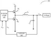
参考图1,所示为一采用降压型拓扑结构的开关电源的原理框图。其中,功率器件M1,功率器件M2,电感L1和电容C1组成一降压型的功率级电路,以将输入电压Vin转换为输出电压Vout来驱动负载101。开关电源100的控制方式为闭环控制方式。反馈电路102接收输出电压Vout,并产生一表征输出电压Vout的反馈信号Vfb;控制和驱动电路103根据接收到的所述反馈信号Vfb和一表征期望输出电压的基准电压Vref产生相应的控制信号,来控制功率器件M1和功率器件M2周期性的开通和断开,以使输出电压Vout维持基本恒定。Referring to Fig. 1, it shows a functional block diagram of a switching power supply using a step-down topology. Wherein, the power device M1 , the power device M2 , the inductor L1 and the capacitor C1 form a step-down power stage circuit to convert the input voltage Vin into an output voltage Vout to drive the load 101 . The control mode of the switching
对集成电路而言,可以通过不同的方式来实现图1所示的开关电源。例如,可以将功率器件M1,功率器件M2和控制和驱动电路103分别制造为一单颗的硅片,然后通过引线在封装内部实现不同硅片之间的电性连接。当然,这类实现方式,不可避免的会产生由引线上的电阻和寄生电感带来的功率损耗。但是,采用这样的实现方式,硅片制造工艺会相对简单一些。For integrated circuits, the switching power supply shown in Figure 1 can be implemented in different ways. For example, the power device M1 , the power device M2 and the control and driving
另外,也可以用一单颗的硅片集成功率器件M1,功率器件M2和控制和驱动电路103。这样的单片集成开关电源由于不需要各功能元件之间的引线连接,因此功能元件间的引线寄生电阻和寄生电感减小。这种方案与各个功能元件相互分离的分立元件解决方案相比较,功能元件间的较低的引线寄生电阻和寄生电感使得单片集成开关电源可以容纳更大的电流密度,并且可以工作在较高的开关频率。但是,这样的实现方式制造工艺复杂,也非常具有难度。In addition, a single silicon chip can also be used to integrate the power device M1 , the power device M2 and the control and driving
不管采用哪种集成方式,最后都需要对硅片进行封装,以实现集成电路硅片与外部之间的电气连接,以及为集成电路芯片提供一个稳定可靠的工作环境,并对集成电路硅片起到机械或环境保护的作用。对开关电源类集成电路的封装而言,通常均需要三个引脚来实现与外部的电气连接,输入引脚IN用以接收输入电压Vin,接地引脚GND用以给集成电路芯片提供一地电位,输出引脚LX用以输出一定的电信号来驱动负载。No matter which integration method is used, the silicon chip needs to be packaged in the end to realize the electrical connection between the integrated circuit silicon chip and the outside, and to provide a stable and reliable working environment for the integrated circuit chip, and to protect the integrated circuit silicon chip. to the role of mechanical or environmental protection. For the packaging of switching power supply integrated circuits, usually three pins are required to realize the electrical connection with the outside, the input pin IN is used to receive the input voltage Vin , and the ground pin GND is used to provide an integrated circuit chip. The ground potential, the output pin LX is used to output a certain electrical signal to drive the load.
结合图1所示的开关电源的示例,以功率器件M1和功率器件M2为横向双扩散金属氧化物半导体晶体管(LDMOS)为例,输入引脚IN即为功率器件M1的漏极,用以接收输入电压Vin;接地引脚GND即为功率器件M2的源极,用以给集成电路芯片提供一地电位;输出引脚LX即为功率器件M1的源极和功率器件M2的漏极的公共连接点,用以连接电感L1和电容C1,进而输出恒定的输出电信号。Combining the example of the switching power supply shown in Figure 1, taking the power deviceM1 and the power deviceM2 as lateral double-diffused metal-oxide-semiconductor transistors (LDMOS) as an example, the input pin IN is the drain of the power deviceM1 , To receive the input voltage Vin ; the ground pin GND is the source of the power deviceM2 , which is used to provide a ground potential for the integrated circuit chip; the output pin LX is the source of the power deviceM1 and the power device M The common connection point of the drain of2 is used to connect the inductor L1 and the capacitor C1 to output a constant output electrical signal.
依据本发明实施例的倒装芯片封装结构既可以适用于元件分立的集成方式,也可以适用于单片集成的集成方式,可以实际需要进行选择。The flip-chip packaging structure according to the embodiment of the present invention can be applied not only to the integration method of discrete components, but also to the integration method of monolithic integration, which can be selected according to actual needs.
以下将结合实施例,并以图1所示的开关电源为例,详细说明依据本发明的开关电源的倒装封装结构和倒装封装方法。The flip-chip packaging structure and flip-chip packaging method of the switching power supply according to the present invention will be described in detail below with reference to the embodiments and taking the switching power supply shown in FIG. 1 as an example.
实施例一:元件分立的集成方式Embodiment 1: Integration of discrete components
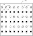
在该实施例中,功率器件M1,功率器件M2和控制和驱动电路103分别为一单颗的硅片。以连接重分布层和硅片以及重分布层和引线框架的凸块为焊垫以及其上的焊锡球为例来说明该实施例的倒装封装结构。参考图2,所示为依据本发明一实施例的一功率器件硅片上的焊垫、焊锡球的布置图。硅片201上具有多组焊垫以及焊垫上的焊锡球。其中,焊垫203为源极焊垫,其上的焊锡球202为源极焊锡球;焊垫205为漏极焊垫,其上的焊锡球204为漏极焊锡球。焊锡球202和焊锡球204呈矩阵排列。In this embodiment, the power device M1 , the power device M2 and the control and driving
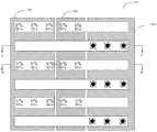
参考图3,所示为依据本发明实施例的图2所示的功率器件硅片的倒装封装结构的重分布层以及引线框架的布置图。其中,重分布层RDL包括一组漏极重分布单元301和一组源极重分布层304。按照焊锡球204的矩阵排列方式,漏极重分布层单元301的第一表面覆盖漏极焊锡球204,并通过第二表面上的焊垫302和焊锡球303,将漏极电极性引至重分布层的左半区域;源极重分布层单元304的第一表面覆盖源极焊锡球202,并通过第二表面上的焊垫305和焊锡球306,将源极电极性引至重分布层的右半区域,从而将漏极电极性和源极电极性分割为两个独立并且相互不重叠的区域。Referring to FIG. 3 , it is a layout diagram of the redistribution layer and the lead frame of the flip-chip packaging structure of the power device silicon chip shown in FIG. 2 according to an embodiment of the present invention. Wherein, the redistribution layer RDL includes a set of
然后,引线框架的每一引脚的第一表面覆盖相同电极性的焊锡球,从而使每一引脚具有不同的电极性。在图3中,引脚307的第一表面覆盖具有漏极电极性的一组焊锡球303;引脚308的第一表面覆盖具有源极电极性的一组焊锡球305。然后,引线框架再与PCB印刷电路板上的金属层(如铜层)连接,实现了功率器件的漏极和源极与外部的电气连接。Then, the first surface of each pin of the lead frame is covered with solder balls of the same electrical polarity, so that each pin has a different electrical polarity. In FIG. 3 , a first surface of a
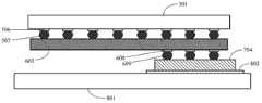
参考图4A,所示为图3所示的依据本发明实施例的功率器件硅片的倒装封装结构沿轴线B-B’的剖面图。硅片201(功率器件)倒置,其第一表面上的焊垫205和焊锡球204与重分布层单元301的第一表面连接;重分布层单元301的第二表面上的焊垫302和焊锡球303与引线框架的引脚307的第一表面连接;引脚307的第二表面与PCB板402上的金属层401连接。Referring to FIG. 4A , it is a cross-sectional view along the axis B-B' of the flip-chip packaging structure of the power device silicon chip shown in FIG. 3 according to the embodiment of the present invention. The silicon chip 201 (power device) is turned upside down, and the
通过一组重分布层单元301将漏极电极性从分散于硅片201的整个区域转移至硅片201的整左侧区域,从而PCB板的金属层401以及引线框架的引脚307的面积和厚度可以设置为较大的数值,在实现硅片201与外部的电气连接的同时,也减小了电流传导路径的电阻,降低了功率损耗,提高了开关电源的效率。Through a group of
参考图4B,所示为图3所示的依据本发明实施例的功率器件硅片的倒装封装结构沿轴线A-A’的剖面图。硅片201(功率器件)倒置,其第一表面上的焊垫203和焊锡球202与重分布层单元304的第一表面连接;重分布层单元304的第二表面上的焊垫305和焊锡球306与引线框架的引脚308的第一表面连接;引脚308的第二表面与PCB板402上的金属层403连接。Referring to FIG. 4B , it is a cross-sectional view along the axis A-A' of the flip-chip packaging structure of the power device silicon chip shown in FIG. 3 according to the embodiment of the present invention. The silicon wafer 201 (power device) is turned upside down, and the solder pads 203 and solder balls 202 on the first surface are connected to the first surface of the
通过一组重分布层单元304将源极电极性从分散于硅片201的整个区域转移至硅片201的整右侧区域,从而PCB板的金属层403以及引线框架的引脚308的面积和厚度可以设置为较大的数值,在实现硅片201与外部的电气连接的同时,也减小了电流传导路径的电阻,降低了功率损耗,提高了开关电源的效率。The polarity of the source electrode is transferred from the entire area scattered on the
并且,通过调整功率器件的面积,功率器件区域可以扩展或者缩小,倒装封装结构的尺寸可以成比例进行调节。因此对于不同额定电流的功率器件,简化了产品系列的设计,简化了封装工艺,增强了通用性。Moreover, by adjusting the area of the power device, the area of the power device can be expanded or reduced, and the size of the flip-chip package structure can be adjusted proportionally. Therefore, for power devices with different rated currents, the design of product series is simplified, the packaging process is simplified, and the versatility is enhanced.
在该实施例中,功率器件可以是任何合适类型的晶体管,如横向双扩散金属氧化物半导体晶体管(LDMOS)。引线框架的材料可以是任何合适的材料(如铜合金等)。同样,倒装封装结构可以是方形扁平无引脚封装(QFN)或者双排平面无引脚封装(DFN),或者任何其他合适的封装。进一步,用以连接重分布层和硅片以及重分布层和引线框架的凸块也可用任何合适的技术(如铜柱、锡、化学镍金等)。In this embodiment, the power device may be any suitable type of transistor, such as a lateral double diffused metal oxide semiconductor transistor (LDMOS). The material of the lead frame can be any suitable material (such as copper alloy, etc.). Likewise, the flip-chip package structure may be a quad flat no-leads (QFN) or dual flat no-leads (DFN), or any other suitable package. Further, the bumps used to connect the RDL to the silicon chip and the RDL to the lead frame can also use any suitable technology (such as copper pillars, tin, chemical nickel gold, etc.).
实施例二:单片集成的集成方式Embodiment 2: Integration method of monolithic integration
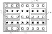
采用这种集成方式,两个功率器件以及控制和驱动电路集成于一单颗的硅片中。由于不需要控制和驱动电路和功率器件之间的引线连接,因此各功能元件之间的引线上的寄生电阻和寄生电感减小。以连接重分布层和硅片以及重分布层和引线框架的凸块为焊垫以及其上的焊锡球为例来说明该实施例的倒装封装结构。参考图5,所示为依据本发明另一实施例的单片开关电源硅片上的焊垫、焊锡球的布置图。其中,硅片501包括两个并列排列的功率器件,以及控制和驱动电路。在此,为方便说明,仅仅列出了功率器件的焊垫以及焊锡球的布置方式,控制和驱动电路的焊垫以及焊锡球的布置方式在此不进行详细说明。With this integration method, two power devices as well as control and drive circuits are integrated in a single silicon chip. Since lead connections between control and drive circuits and power devices are not required, parasitic resistance and inductance on leads between functional elements are reduced. The flip-chip packaging structure of this embodiment is illustrated by taking the bumps connecting the redistribution layer and the silicon chip and the bumps connecting the redistribution layer and the lead frame as solder pads and solder balls thereon as examples. Referring to FIG. 5 , it is a layout diagram of pads and solder balls on a monolithic switching power supply silicon chip according to another embodiment of the present invention. Wherein, the
硅片501的第一表面上设置有多组焊垫以及焊垫上的焊锡球,并且,这些焊垫和焊锡球呈矩阵排列。其中,输入焊垫502以及输入焊垫之上的输入焊锡球503与接地焊垫504以及接地焊垫之上的接地焊锡球505位于同一行,并与一组输出焊垫506以及输出焊垫之上的输出焊锡球507相互间隔,依次排列。Multiple groups of solder pads and solder balls on the solder pads are disposed on the first surface of the
参考图6,所示为依据本发明实施例的图5所示的单片开关电源硅片的倒装封装结构的重分布层的布置图。按照矩阵排列结构,重分布层RDL的重分布层单元将输入焊锡球503,输出焊锡球507,接地焊锡球505重新进行排列分布。重分布层的第一表面分别与输入焊锡球IN,输出焊锡球LX,接地焊锡球GND进行相应的连接;重分布层的第二表面上具有另一组焊垫和焊锡球,以将硅片501上的输入,输出和接地三种电极性重新进行排列分布,以方便于引脚排列,并且最大程度的减小电流传导路径的电阻。具体的,重分布层单元601的第一表面完全覆盖输入焊锡球503,第二表面上布置有第二组焊垫604以及其上的焊锡球605,以将输入电极性IN转移至硅片区域的左侧区域。重分布层单元602的第一表面完全覆盖接地焊锡球505,第二表面上布置有焊垫606以及其上的焊锡球607,以将接地电极性GND转移至硅片区域的中间区域。重分布层单元603的第一表面完全覆盖输出焊锡球507,第二表面上布置有焊垫608以及其上的焊锡球609,以将输出电极性LX转移至硅片区域的右侧区域。Referring to FIG. 6 , it is a layout diagram of the redistribution layer of the flip-chip packaging structure of the monolithic switching power supply silicon chip shown in FIG. 5 according to an embodiment of the present invention. According to the matrix arrangement structure, the redistribution layer unit of the redistribution layer RDL will input
参考图7,所示为依据本发明实施例的图5所示的单片开关电源硅片的倒装封装结构的引线框架的布置图。如图6所示,利用重分布层RDL已经将不同电极性进行了重新分布,输入电极性位于硅片区域的左侧区域,接地电极性位于硅片区域的中间区域,输出电极性位于硅片区域的右侧区域。因此,引线框架的输入引脚702,输出引脚704和接地引脚703可以表现为三个整片的金属层结构。例如,引线框架的引脚可以设置为具有较厚厚度的铜金属层。这样不仅为硅片和重分布层提供很好的机械支撑,而且,较厚的金属层也可以使作为电流传导路径的组成部分的引脚具有较小的电阻。Referring to FIG. 7 , it is a layout diagram of the lead frame of the flip-chip packaging structure of the monolithic switching power supply silicon chip shown in FIG. 5 according to an embodiment of the present invention. As shown in Figure 6, different electrical polarities have been redistributed by using the redistribution layer RDL. The input electrical polarity is located in the left area of the silicon wafer area, the ground electrical polarity is located in the middle area of the silicon wafer area, and the output electrical polarity is located in the silicon wafer area. The right side of the region. Therefore, the
参考图8A,所示为图7所示的依据本发明实施例的单片开关电源的倒装封装结构沿轴线A-A’的剖面图。其中,硅片501倒置,其上的输出焊垫506以及输出焊锡球507连接至重分布层单元603的第一表面。重分布层单元603的第二表面上的焊垫608以及焊锡球609连接至引线框架的引脚704的第一表面;引脚704的第二表面连接至PCB板801上的金属层802。Referring to FIG. 8A , it is a cross-sectional view along the axis A-A' of the flip-chip packaging structure of the monolithic switching power supply shown in FIG. 7 according to the embodiment of the present invention. Wherein, the
参考图8B,所示为图7所示的依据本发明实施例的单片开关电源的倒装封装结构沿轴线B-B’的剖面图。其中,硅片501倒置,其上的输入焊垫502以及输入焊锡球503连接至重分布层单元601的第一表面。重分布层单元601的第二表面上的焊垫604以及焊锡球605连接至引线框架的引脚702的第一表面;引脚702的第二表面连接至PCB板801上的金属层803。硅片501上的接地焊垫504以及接地焊锡球505连接至重分布层单元602的第一表面。重分布层单元602的第二表面上的焊垫606以及焊锡球607连接至引线框架的引脚703的第一表面;引脚703的第二表面连接至PCB板801上的金属层804。Referring to FIG. 8B , it is a cross-sectional view along the axis B-B' of the flip-chip packaging structure of the monolithic switching power supply shown in FIG. 7 according to the embodiment of the present invention. Wherein, the
依据本发明实施例的上述单片开关电源的倒装封装结构,根据特定的开关电源硅片的电路布置和相关联的PCB路径,通过相应的重分布层结构,对各不同的电极性进行重新分布,使得电极性能够集中分布,便于引脚和PCB板的金属层的布设。进而,引脚和PCB板的金属层可以设置为具有较大面积和较厚厚度的金属层,以减小电流导电路径的电阻,提高传输路径的传导效率。According to the flip-chip packaging structure of the above-mentioned monolithic switching power supply in the embodiment of the present invention, according to the circuit layout of the specific switching power supply silicon chip and the associated PCB path, through the corresponding redistribution layer structure, the different electrical polarities are redistributed. Distribution, so that the electrical polarity can be distributed in a concentrated manner, which is convenient for the layout of the pins and the metal layer of the PCB board. Furthermore, the metal layer of the pin and the PCB board can be set as a metal layer with a larger area and a thicker thickness, so as to reduce the resistance of the current conduction path and improve the conduction efficiency of the transmission path.
另一方面,倒装封装结构的尺寸可以成比例进行调节。通过调整功率器件的面积,功率器件区域可以扩展或者缩小。因此对于不同额定电流的功率器件,简化了产品系列的设计,简化了封装工艺,增强了通用性。On the other hand, the size of the flip-chip package structure can be adjusted proportionally. By adjusting the area of the power device, the area of the power device can be expanded or reduced. Therefore, for power devices with different rated currents, the design of product series is simplified, the packaging process is simplified, and the versatility is enhanced.
以上详细说明了依据本发明一实施例的重分布层、引线框架、PCB板的铜金属层的布设方式。本领域技术人员可以得知,其他合适形式的布设方式也同样适用于本发明的倒装封装结构。The layout of the redistribution layer, the lead frame, and the copper metal layer of the PCB board according to an embodiment of the present invention has been described in detail above. Those skilled in the art can know that other suitable arrangements are also applicable to the flip-chip packaging structure of the present invention.
参考图9,所示为依据本发明一实施例的单片开关电源硅片的倒装封装结构的示意图。在该实施例中,通过重分布层对输入、输出和接地三种电极性进行重新分配,然后通过引线框架的引脚将这三种电极性引出。其中,引脚902(GND)不是规则的矩形形状,而是根据重分布层的结构表现为相应的形状,并且三个引脚(输入引脚901,接地引脚902和输出引脚903)的区域不互相重叠,具体表示为“E”形状。Referring to FIG. 9 , it is a schematic diagram of a flip-chip packaging structure of a monolithic switching power supply silicon chip according to an embodiment of the present invention. In this embodiment, the three electrical polarities of input, output and ground are redistributed through the redistribution layer, and then these three electrical polarities are led out through the pins of the lead frame. Among them, the pin 902 (GND) is not a regular rectangular shape, but behaves in a corresponding shape according to the structure of the redistribution layer, and the three pins (
参考图10,所示为依据本发明另一实施例的单片开关电源硅片的倒装封装结构的示意图。在该实施例中,重分布层单元可以覆盖单个的焊垫以及焊锡球,也可以横跨行或者列以将不同行或者列中相同电极性的焊锡球连接起来,并将不同的电极性转移至不同的区域。例如,位于左侧区域的输入引脚1001(IN),位于中间区域的接地引脚1002(GND)和位于右侧区域的输出引脚1003(LX)。Referring to FIG. 10 , it is a schematic diagram of a flip-chip packaging structure of a monolithic switching power supply silicon chip according to another embodiment of the present invention. In this embodiment, the redistribution layer unit can cover a single pad and solder ball, and can also span rows or columns to connect solder balls of the same electrical polarity in different rows or columns, and transfer different electrical polarities to different regions. For example, an input pin 1001 (IN) located in the left area, a ground pin 1002 (GND) located in the middle area, and an output pin 1003 (LX) located in the right area.
以下结合实施例详细说明依据本发明的集成开关电源的倒装封装方法。The flip-chip packaging method of the integrated switching power supply according to the present invention will be described in detail below in conjunction with the embodiments.
参考图11,所示为依据本发明一实施例的集成开关电源的倒装封装方法的流程图。在该实施例中,集成开关电源的倒装封装方法包括以下步骤:Referring to FIG. 11 , it is a flow chart of a flip-chip packaging method for an integrated switching power supply according to an embodiment of the present invention. In this embodiment, the flip-chip packaging method of an integrated switching power supply includes the following steps:
S1101:提供一个或者多个硅片,所述硅片的第一表面包括一组第一组凸块,所述第一组凸块具有至少两种以上的电极性;S1101: Provide one or more silicon chips, the first surface of the silicon chip includes a first group of bumps, and the first group of bumps has at least two or more electrical polarities;
S1102:在所述硅片上布设一重分布层,所述重分布层包括一组重分布层单元,所述重分布层单元的第一表面用以连接所述第一组凸块中的电极性相同的凸块;所述重分布层单元的第二表面包括一组第二组凸块,所述第二组凸块用以将所述电极性进行重新排布;S1102: Laying a redistribution layer on the silicon wafer, the redistribution layer includes a group of redistribution layer units, the first surface of the redistribution layer unit is used to connect the electrical polarities in the first group of bumps the same bumps; the second surface of the redistribution layer unit includes a second group of bumps, the second group of bumps is used to rearrange the electrical polarity;
S1103:在所述重分布层上布设一引线框架,所述引线框架包括一组引脚,所述引脚的第一表面与所述第二组凸块中的电极性相同的凸块连接,以使所述引脚具有相应的电极性;S1103: Lay a lead frame on the redistribution layer, where the lead frame includes a set of pins, and the first surface of the pins is connected to bumps with the same electrical polarity in the second set of bumps, so that said pins have a corresponding electrical polarity;
S1104:利用一倒装片封装结构将所述硅片、所述第一组凸块、所述第二组凸块和所述引线框架进行封装,并利用所述引线框架的第二表面来实现所述集成开关电源与外部PCB板之间的电气连接。S1104: Package the silicon wafer, the first group of bumps, the second group of bumps, and the lead frame using a flip-chip packaging structure, and use the second surface of the lead frame to implement The electrical connection between the integrated switching power supply and the external PCB board.
进一步的,所述第一组凸块可以设置为规则的矩阵排列。因此,在步骤S1102中,按照矩阵的行或者列,将相同行或者列中的具有相同电极性的第一组凸块中的凸块利用一组呈矩形形状的重分布层单元的第一表面将其分别连接起来。当然也可以跨越不同的行或者列,将不同行或者列中的具有相同电极性的第一组凸块中的凸块利用一完整的重分布层单元的第一表面将其分别连接起来,此时重分布层单元不是规则的几何形状。Further, the first group of bumps can be arranged in a regular matrix. Therefore, in step S1102, according to the rows or columns of the matrix, the bumps in the first group of bumps with the same electrical polarity in the same row or column are used on the first surface of a group of rectangular redistribution layer units Connect them separately. Of course, the bumps in the first group of bumps with the same electrical polarity in different rows or columns can also be connected across different rows or columns by using the first surface of a complete redistribution layer unit. The time redistribution layer units are not regular geometric shapes.
另一方面,重分布层单元的第二表面的第二组凸块也相应的具有了与第一组凸块相同的电极性。通过对所述第二组凸块的排布,将具有相同电极性的第二组凸块中的凸块转移至一相对集中的区域。例如,可以是沿着所述硅片区域的一边界依次间隔,平行排列;或者,保证各电极性区域互不重叠,相互间隔,并且方便于后续引线框架的引脚的设置。On the other hand, the second group of bumps on the second surface of the RDL unit also correspondingly have the same electrical polarity as the first group of bumps. Through the arrangement of the second group of bumps, the bumps in the second group of bumps with the same electrical polarity are transferred to a relatively concentrated area. For example, it may be spaced apart and arranged in parallel along a boundary of the silicon wafer region; or, it is ensured that the electric polar regions do not overlap with each other and are spaced apart from each other, which facilitates the arrangement of leads of the subsequent lead frame.
在步骤S1103中,引线框架的一组引脚的第一表面分别覆盖第二组凸块中具有相同电极性的凸块,从而将电极性通过所述引脚分别对外引出。由于重分布层对电极性的重新排布,使得具有相同电极性的第二组凸块区域相对集中,因此,引脚的布置可以相对简单一些,并且,引脚可以设置为具有较大面积和较厚厚度的金属层,从而降低电流传导路径的电阻,减少损耗。对开关电源而言,需要传导较大电流的路径包括输入引脚,输出引脚和接地引脚。In step S1103 , the first surfaces of a group of pins of the lead frame respectively cover the bumps with the same electrical polarity in the second group of bumps, so that the electrical polarities are drawn out through the pins respectively. Due to the rearrangement of the polarity of the redistribution layer, the second group of bump regions with the same polarity are relatively concentrated, so the arrangement of the pins can be relatively simple, and the pins can be set to have a larger area and A thicker metal layer reduces the resistance of the current conduction path and reduces losses. For switching power supplies, the paths that need to conduct large currents include input pins, output pins, and ground pins.
在步骤S1104中,还可以在PCB(印刷电路板)上设置不同的金属层,来分别与所述引线框架的不同引脚的第二表面连接,相应的,所述金属层同样可以设置具有较大的面积,来减低电阻。In step S1104, different metal layers can also be set on the PCB (printed circuit board) to respectively connect with the second surfaces of different pins of the lead frame. large area to reduce resistance.
以上对依据本发明的优选实施例的集成开关电源的倒装封装结构和倒装封装方法进行了详尽描述,本领域普通技术人员据此可以推知其他技术或者结构以及电路布局、元件等均可应用于所述实施例,例如,功率器件的类型,引线框架的材料,倒装封装结构的类型,以及凸块的构成可以为任何合适的形式。上述实施例中,并没有详细说明倒装片封装结构,本领域技术人员可以得知任何合适类型的塑封结构,如为方形扁平无引脚封装(QFN)结构或者双排平面无引脚封装(DFN)结构均适用于依据本发明的倒装封装结构。The flip-chip packaging structure and flip-chip packaging method of the integrated switching power supply according to the preferred embodiment of the present invention have been described in detail above, and those of ordinary skill in the art can deduce that other technologies or structures, circuit layouts, components, etc. can be applied Depending on the embodiment, for example, the type of power device, the material of the lead frame, the type of flip-chip package structure, and the configuration of the bumps may be in any suitable form. In the above embodiments, the flip-chip packaging structure is not described in detail, and those skilled in the art can know any suitable type of plastic packaging structure, such as a quad flat no-lead package (QFN) structure or a double-row planar no-lead package ( DFN) structures are applicable to the flip-chip packaging structure according to the present invention.
在本文中,诸如第一和第二等之类的关系术语仅仅用来将一个实体或者操作与另一个实体或操作区分开来,而不一定要求或者暗示这些实体或操作之间存在任何这种实际的关系或者顺序。而且,术语“包括”、“包含”或者其任何其他变体意在涵盖非排他性的包含,从而使得包括一系列要素的过程、方法、物品或者设备不仅包括那些要素,而且还包括没有明确列出的其他要素,或者是还包括为这种过程、方法、物品或者设备所固有的要素。在没有更多限制的情况下,由语句“包括一个……”限定的要素,并不排除在包括所述要素的过程、方法、物品或者设备中还存在另外的相同要素。In this document, relational terms such as first and second etc. are used only to distinguish one entity or operation from another without necessarily requiring or implying any such relationship between these entities or operations. Actual relationship or sequence. Furthermore, the term "comprises", "comprises" or any other variation thereof is intended to cover a non-exclusive inclusion such that a process, method, article, or apparatus comprising a set of elements includes not only those elements, but also includes elements not expressly listed. other elements of or also include elements inherent in such a process, method, article, or device. Without further limitations, an element defined by the phrase "comprising a ..." does not exclude the presence of additional identical elements in the process, method, article or apparatus comprising said element.
依照本发明的实施例如上文所述,这些实施例并没有详尽叙述所有的细节,也不限制该发明仅为所述的具体实施例。显然,根据以上描述,可作很多的修改和变化。本说明书选取并具体描述这些实施例,是为了更好地解释本发明的原理和实际应用,从而使所属技术领域技术人员能很好地利用本发明以及在本发明基础上的修改使用。本发明仅受权利要求书及其全部范围和等效物的限制。Embodiments according to the present invention are described above, and these embodiments do not describe all details in detail, nor do they limit the invention to only the specific embodiments described. Obviously many modifications and variations are possible in light of the above description. This description selects and specifically describes these embodiments in order to better explain the principles and practical applications of the present invention, so that those skilled in the art can make good use of the present invention and its modification on the basis of the present invention. The invention is to be limited only by the claims, along with their full scope and equivalents.
Claims (18)
Translated fromChinesePriority Applications (4)
| Application Number | Priority Date | Filing Date | Title |
|---|---|---|---|
| CN201210335201.8ACN102842564B (en) | 2012-09-12 | 2012-09-12 | Flip-chip package device for integrated switching power supply and flip-chip packaging method |
| TW102120539ATWI512937B (en) | 2012-09-12 | 2013-06-10 | Flip - mounted package for integrated switching power supply and its flip - chip packaging method |
| US14/018,206US9024440B2 (en) | 2012-09-12 | 2013-09-04 | Flip-chip package structure and method for an integrated switching power supply |
| US14/672,512US9245872B2 (en) | 2012-09-12 | 2015-03-30 | Flip-chip package structure and method for an integrated switching power supply |
Applications Claiming Priority (1)
| Application Number | Priority Date | Filing Date | Title |
|---|---|---|---|
| CN201210335201.8ACN102842564B (en) | 2012-09-12 | 2012-09-12 | Flip-chip package device for integrated switching power supply and flip-chip packaging method |
Publications (2)
| Publication Number | Publication Date |
|---|---|
| CN102842564A CN102842564A (en) | 2012-12-26 |
| CN102842564Btrue CN102842564B (en) | 2014-06-25 |
Family
ID=47369783
Family Applications (1)
| Application Number | Title | Priority Date | Filing Date |
|---|---|---|---|
| CN201210335201.8AActiveCN102842564B (en) | 2012-09-12 | 2012-09-12 | Flip-chip package device for integrated switching power supply and flip-chip packaging method |
Country Status (3)
| Country | Link |
|---|---|
| US (2) | US9024440B2 (en) |
| CN (1) | CN102842564B (en) |
| TW (1) | TWI512937B (en) |
Families Citing this family (11)
| Publication number | Priority date | Publication date | Assignee | Title |
|---|---|---|---|---|
| JP6336293B2 (en)* | 2014-02-21 | 2018-06-06 | ローム株式会社 | Voltage generator |
| US9379079B1 (en)* | 2014-12-29 | 2016-06-28 | Mediatek Inc. | Flip chip scheme and method of forming flip chip scheme |
| JP6019367B2 (en)* | 2015-01-13 | 2016-11-02 | 株式会社野田スクリーン | Semiconductor device |
| WO2017027101A1 (en) | 2015-08-13 | 2017-02-16 | Exxonmobil Chemical Patents Inc. | Multi-layered sheets comprising a high melt strength polypropylene |
| JP6653541B2 (en) | 2015-09-14 | 2020-02-26 | ローム株式会社 | Semiconductor device |
| KR102389772B1 (en)* | 2015-12-03 | 2022-04-21 | 삼성전자주식회사 | Semiconductor device and method for fabricating the same |
| CN107393836B (en) | 2017-06-19 | 2020-04-10 | 矽力杰半导体技术(杭州)有限公司 | Chip packaging method and packaging structure |
| CN107808868B (en) | 2017-10-13 | 2020-03-10 | 矽力杰半导体技术(杭州)有限公司 | Chip packaging structure and manufacturing method thereof |
| CN110323141B (en) | 2019-04-15 | 2021-10-12 | 矽力杰半导体技术(杭州)有限公司 | Lead frame structure, chip packaging structure and manufacturing method thereof |
| CN110534494B (en)* | 2019-09-06 | 2020-11-06 | 深圳市安信达存储技术有限公司 | BGA chip pin secondary arrangement packaging method and packaging structure |
| CN114267656A (en)* | 2021-06-02 | 2022-04-01 | 青岛昇瑞光电科技有限公司 | Packaging structure and packaging method of power module |
Family Cites Families (24)
| Publication number | Priority date | Publication date | Assignee | Title |
|---|---|---|---|---|
| US6130546A (en)* | 1998-05-11 | 2000-10-10 | Lsi Logic Corporation | Area array (flip chip) probe card |
| US6713860B2 (en)* | 2002-02-01 | 2004-03-30 | Intel Corporation | Electronic assembly and system with vertically connected capacitors |
| TW586205B (en)* | 2001-06-26 | 2004-05-01 | Intel Corp | Electronic assembly with vertically connected capacitors and manufacturing method |
| US6800947B2 (en)* | 2001-06-27 | 2004-10-05 | Intel Corporation | Flexible tape electronics packaging |
| CN1194410C (en)* | 2001-12-21 | 2005-03-23 | 威盛电子股份有限公司 | Flip Chip Conductive Bump and Redistribution Wire Layer Configuration |
| AU2003298595A1 (en)* | 2002-10-08 | 2004-05-04 | Chippac, Inc. | Semiconductor stacked multi-package module having inverted second package |
| US6900538B2 (en)* | 2003-06-03 | 2005-05-31 | Micrel, Inc. | Integrating chip scale packaging metallization into integrated circuit die structures |
| US6875921B1 (en)* | 2003-10-31 | 2005-04-05 | Xilinx, Inc. | Capacitive interposer |
| US7566960B1 (en)* | 2003-10-31 | 2009-07-28 | Xilinx, Inc. | Interposing structure |
| US20050133929A1 (en)* | 2003-12-18 | 2005-06-23 | Howard Gregory E. | Flexible package with rigid substrate segments for high density integrated circuit systems |
| US7078812B2 (en)* | 2004-08-30 | 2006-07-18 | Hewlett-Packard Development Company, L.P. | Routing differential signal lines in a substrate |
| JP2006216758A (en)* | 2005-02-03 | 2006-08-17 | Three M Innovative Properties Co | Connection method of printed circuit board |
| US7944048B2 (en)* | 2006-08-09 | 2011-05-17 | Monolithic Power Systems, Inc. | Chip scale package for power devices and method for making the same |
| US8237289B2 (en)* | 2007-01-30 | 2012-08-07 | Kabushiki Kaisha Toshiba | System in package device |
| US7595226B2 (en)* | 2007-08-29 | 2009-09-29 | Freescale Semiconductor, Inc. | Method of packaging an integrated circuit die |
| US7838975B2 (en)* | 2008-05-27 | 2010-11-23 | Mediatek Inc. | Flip-chip package with fan-out WLCSP |
| US8110926B2 (en)* | 2009-01-30 | 2012-02-07 | Broadcom Corporation | Redistribution layer power grid |
| US8390035B2 (en)* | 2009-05-06 | 2013-03-05 | Majid Bemanian | Massively parallel interconnect fabric for complex semiconductor devices |
| CN102481598B (en)* | 2009-06-11 | 2014-07-09 | 罗杰斯公司 | Dielectric material, method of forming subassembly therefrom, and subassembly formed thereby |
| US8084780B2 (en)* | 2009-08-13 | 2011-12-27 | Semileds Optoelectronics Co. | Smart integrated semiconductor light emitting system including light emitting diodes and application specific integrated circuits (ASIC) |
| US20110241125A1 (en)* | 2010-03-31 | 2011-10-06 | Semtech Corporation | Power Semiconductor Device with Low Parasitic Metal and Package Resistance |
| TWI418269B (en)* | 2010-12-14 | 2013-12-01 | Unimicron Technology Corp | Package substrate with embedded perforation interposer and preparation method thereof |
| US8546925B2 (en)* | 2011-09-28 | 2013-10-01 | Texas Instruments Incorporated | Synchronous buck converter having coplanar array of contact bumps of equal volume |
| TWI508258B (en)* | 2013-12-19 | 2015-11-11 | 矽品精密工業股份有限公司 | Semiconductor package and manufacturing method thereof |
- 2012
- 2012-09-12CNCN201210335201.8Apatent/CN102842564B/enactiveActive
- 2013
- 2013-06-10TWTW102120539Apatent/TWI512937B/enactive
- 2013-09-04USUS14/018,206patent/US9024440B2/enactiveActive
- 2015
- 2015-03-30USUS14/672,512patent/US9245872B2/enactiveActive
Also Published As
| Publication number | Publication date |
|---|---|
| US9245872B2 (en) | 2016-01-26 |
| CN102842564A (en) | 2012-12-26 |
| TW201413912A (en) | 2014-04-01 |
| TWI512937B (en) | 2015-12-11 |
| US9024440B2 (en) | 2015-05-05 |
| US20150206857A1 (en) | 2015-07-23 |
| US20140070385A1 (en) | 2014-03-13 |
Similar Documents
| Publication | Publication Date | Title |
|---|---|---|
| CN102842564B (en) | Flip-chip package device for integrated switching power supply and flip-chip packaging method | |
| US8400778B2 (en) | Layout schemes and apparatus for multi-phase power switch-mode voltage regulator | |
| US8461669B2 (en) | Integrated power converter package with die stacking | |
| US9129947B2 (en) | Multi-chip packaging structure and method | |
| US8400784B2 (en) | Flip chip package for monolithic switching regulator | |
| US9111928B2 (en) | Switch circuit package module | |
| US20140063744A1 (en) | Vertically Stacked Power FETS and Synchronous Buck Converter Having Low On-Resistance | |
| TW201250978A (en) | Multi-die packages structure, converter module and packaging methods | |
| US11742268B2 (en) | Package structure applied to power converter | |
| US9076778B2 (en) | Semiconductor package | |
| TW201230290A (en) | Semiconductor device with stacked power converter | |
| JP4694539B2 (en) | Output control device, and AC / DC power supply device, circuit device, LED backlight circuit device, and switching type DC / DC converter device using the same | |
| TWI492353B (en) | Dual power converter package using external driver ic | |
| CN103928431B (en) | A kind of flip-chip packaged device | |
| TWI555157B (en) | Integrated dual power converter package with internal driver IC | |
| CN211828761U (en) | Packaging structure applied to power converter | |
| CN103985694B (en) | Integrated circuit package and package assembling thereof | |
| JP5412559B2 (en) | Manufacturing method of semiconductor device | |
| JP2009038956A (en) | Output control device | |
| TWM424596U (en) | Semiconductor packaging structure for direct current buck power converter |
Legal Events
| Date | Code | Title | Description |
|---|---|---|---|
| C06 | Publication | ||
| PB01 | Publication | ||
| C10 | Entry into substantive examination | ||
| SE01 | Entry into force of request for substantive examination | ||
| C14 | Grant of patent or utility model | ||
| GR01 | Patent grant | ||
| CP02 | Change in the address of a patent holder | ||
| CP02 | Change in the address of a patent holder | Address after:310051 No. 6 Lianhui Street, Xixing Street, Binjiang District, Hangzhou City, Zhejiang Province Patentee after:Silergy Semiconductor Technology (Hangzhou ) Co., Ltd. Address before:310012 Wensanlu Road, Hangzhou Province, No. 90 East Software Park, science and technology building A1501 Patentee before:Silergy Semiconductor Technology (Hangzhou ) Co., Ltd. |