CN102792455A - Rear-contact heterojunction photovoltaic cell - Google Patents
Rear-contact heterojunction photovoltaic cellDownload PDFInfo
- Publication number
- CN102792455A CN102792455ACN2010800638402ACN201080063840ACN102792455ACN 102792455 ACN102792455 ACN 102792455ACN 2010800638402 ACN2010800638402 ACN 2010800638402ACN 201080063840 ACN201080063840 ACN 201080063840ACN 102792455 ACN102792455 ACN 102792455A
- Authority
- CN
- China
- Prior art keywords
- substrate
- amorphous silicon
- passivation layer
- hydrogenated amorphous
- type
- Prior art date
- Legal status (The legal status is an assumption and is not a legal conclusion. Google has not performed a legal analysis and makes no representation as to the accuracy of the status listed.)
- Pending
Links
- 239000000758substrateSubstances0.000claimsabstractdescription84
- 238000002161passivationMethods0.000claimsabstractdescription61
- 239000004065semiconductorSubstances0.000claimsabstractdescription43
- 229910021417amorphous siliconInorganic materials0.000claimsdescription63
- 229910052782aluminiumInorganic materials0.000claimsdescription15
- XAGFODPZIPBFFR-UHFFFAOYSA-NaluminiumChemical compound[Al]XAGFODPZIPBFFR-UHFFFAOYSA-N0.000claimsdescription14
- 238000005224laser annealingMethods0.000claimsdescription13
- XUIMIQQOPSSXEZ-UHFFFAOYSA-NSiliconChemical compound[Si]XUIMIQQOPSSXEZ-UHFFFAOYSA-N0.000claimsdescription11
- 229910052710siliconInorganic materials0.000claimsdescription11
- 239000010703siliconSubstances0.000claimsdescription11
- 230000015572biosynthetic processEffects0.000claimsdescription10
- 238000005516engineering processMethods0.000claimsdescription9
- 239000004411aluminiumSubstances0.000claimsdescription6
- 239000013078crystalSubstances0.000claimsdescription6
- HQVNEWCFYHHQES-UHFFFAOYSA-Nsilicon nitrideChemical compoundN12[Si]34N5[Si]62N3[Si]51N64HQVNEWCFYHHQES-UHFFFAOYSA-N0.000claimsdescription5
- 238000001704evaporationMethods0.000claimsdescription4
- 230000008020evaporationEffects0.000claimsdescription4
- 238000005507sprayingMethods0.000claimsdescription4
- 238000007650screen-printingMethods0.000claimsdescription3
- 238000001259photo etchingMethods0.000claims1
- 238000001465metallisationMethods0.000abstractdescription37
- 238000000034methodMethods0.000abstractdescription17
- 238000004519manufacturing processMethods0.000abstractdescription12
- 239000000370acceptorSubstances0.000abstractdescription4
- 229910052751metalInorganic materials0.000description18
- 239000002184metalSubstances0.000description18
- 239000002800charge carrierSubstances0.000description8
- 238000000151depositionMethods0.000description7
- 239000000463materialSubstances0.000description7
- 238000006243chemical reactionMethods0.000description4
- 229910021419crystalline siliconInorganic materials0.000description4
- 238000009792diffusion processMethods0.000description4
- 239000002019doping agentSubstances0.000description4
- 239000003574free electronSubstances0.000description4
- 150000003376siliconChemical class0.000description4
- 230000003068static effectEffects0.000description4
- 230000003667anti-reflective effectEffects0.000description3
- 239000011521glassSubstances0.000description3
- 238000004518low pressure chemical vapour depositionMethods0.000description3
- 230000008018meltingEffects0.000description3
- 238000002844meltingMethods0.000description3
- 238000000623plasma-assisted chemical vapour depositionMethods0.000description3
- 239000011347resinSubstances0.000description3
- 229920005989resinPolymers0.000description3
- 238000007711solidificationMethods0.000description3
- 230000008023solidificationEffects0.000description3
- 230000005540biological transmissionEffects0.000description2
- 230000005611electricityEffects0.000description2
- 238000005530etchingMethods0.000description2
- 238000000206photolithographyMethods0.000description2
- 239000007787solidSubstances0.000description2
- VGGSQFUCUMXWEO-UHFFFAOYSA-NEtheneChemical compoundC=CVGGSQFUCUMXWEO-UHFFFAOYSA-N0.000description1
- 239000005977EthyleneSubstances0.000description1
- DGAQECJNVWCQMB-PUAWFVPOSA-MIlexoside XXIXChemical compoundC[C@@H]1CC[C@@]2(CC[C@@]3(C(=CC[C@H]4[C@]3(CC[C@@H]5[C@@]4(CC[C@@H](C5(C)C)OS(=O)(=O)[O-])C)C)[C@@H]2[C@]1(C)O)C)C(=O)O[C@H]6[C@@H]([C@H]([C@@H]([C@H](O6)CO)O)O)O.[Na+]DGAQECJNVWCQMB-PUAWFVPOSA-M0.000description1
- XTXRWKRVRITETP-UHFFFAOYSA-NVinyl acetateChemical compoundCC(=O)OC=CXTXRWKRVRITETP-UHFFFAOYSA-N0.000description1
- 230000004913activationEffects0.000description1
- 239000000919ceramicSubstances0.000description1
- 230000000295complement effectEffects0.000description1
- 238000007796conventional methodMethods0.000description1
- 230000007547defectEffects0.000description1
- 230000000593degrading effectEffects0.000description1
- 238000010586diagramMethods0.000description1
- 239000003989dielectric materialSubstances0.000description1
- 238000009826distributionMethods0.000description1
- 230000005684electric fieldEffects0.000description1
- 238000004070electrodepositionMethods0.000description1
- 238000005538encapsulationMethods0.000description1
- 238000000407epitaxyMethods0.000description1
- 239000012212insulatorSubstances0.000description1
- 238000004093laser heatingMethods0.000description1
- 238000013532laser treatmentMethods0.000description1
- 239000007788liquidSubstances0.000description1
- 230000000873masking effectEffects0.000description1
- 239000007769metal materialSubstances0.000description1
- 150000002739metalsChemical class0.000description1
- 239000000203mixtureSubstances0.000description1
- 229910021421monocrystalline siliconInorganic materials0.000description1
- 229910021420polycrystalline siliconInorganic materials0.000description1
- 238000007789sealingMethods0.000description1
- 229910052708sodiumInorganic materials0.000description1
- 239000011734sodiumSubstances0.000description1
- 238000006467substitution reactionMethods0.000description1
Images


Classifications
- H—ELECTRICITY
- H10—SEMICONDUCTOR DEVICES; ELECTRIC SOLID-STATE DEVICES NOT OTHERWISE PROVIDED FOR
- H10F—INORGANIC SEMICONDUCTOR DEVICES SENSITIVE TO INFRARED RADIATION, LIGHT, ELECTROMAGNETIC RADIATION OF SHORTER WAVELENGTH OR CORPUSCULAR RADIATION
- H10F10/00—Individual photovoltaic cells, e.g. solar cells
- H10F10/10—Individual photovoltaic cells, e.g. solar cells having potential barriers
- H10F10/16—Photovoltaic cells having only PN heterojunction potential barriers
- H—ELECTRICITY
- H10—SEMICONDUCTOR DEVICES; ELECTRIC SOLID-STATE DEVICES NOT OTHERWISE PROVIDED FOR
- H10F—INORGANIC SEMICONDUCTOR DEVICES SENSITIVE TO INFRARED RADIATION, LIGHT, ELECTROMAGNETIC RADIATION OF SHORTER WAVELENGTH OR CORPUSCULAR RADIATION
- H10F19/00—Integrated devices, or assemblies of multiple devices, comprising at least one photovoltaic cell covered by group H10F10/00, e.g. photovoltaic modules
- H10F19/90—Structures for connecting between photovoltaic cells, e.g. interconnections or insulating spacers
- H10F19/902—Structures for connecting between photovoltaic cells, e.g. interconnections or insulating spacers for series or parallel connection of photovoltaic cells
- H—ELECTRICITY
- H10—SEMICONDUCTOR DEVICES; ELECTRIC SOLID-STATE DEVICES NOT OTHERWISE PROVIDED FOR
- H10F—INORGANIC SEMICONDUCTOR DEVICES SENSITIVE TO INFRARED RADIATION, LIGHT, ELECTROMAGNETIC RADIATION OF SHORTER WAVELENGTH OR CORPUSCULAR RADIATION
- H10F71/00—Manufacture or treatment of devices covered by this subclass
- H10F71/128—Annealing
- H—ELECTRICITY
- H10—SEMICONDUCTOR DEVICES; ELECTRIC SOLID-STATE DEVICES NOT OTHERWISE PROVIDED FOR
- H10F—INORGANIC SEMICONDUCTOR DEVICES SENSITIVE TO INFRARED RADIATION, LIGHT, ELECTROMAGNETIC RADIATION OF SHORTER WAVELENGTH OR CORPUSCULAR RADIATION
- H10F71/00—Manufacture or treatment of devices covered by this subclass
- H10F71/129—Passivating
- H—ELECTRICITY
- H10—SEMICONDUCTOR DEVICES; ELECTRIC SOLID-STATE DEVICES NOT OTHERWISE PROVIDED FOR
- H10F—INORGANIC SEMICONDUCTOR DEVICES SENSITIVE TO INFRARED RADIATION, LIGHT, ELECTROMAGNETIC RADIATION OF SHORTER WAVELENGTH OR CORPUSCULAR RADIATION
- H10F77/00—Constructional details of devices covered by this subclass
- H10F77/10—Semiconductor bodies
- H10F77/16—Material structures, e.g. crystalline structures, film structures or crystal plane orientations
- H10F77/162—Non-monocrystalline materials, e.g. semiconductor particles embedded in insulating materials
- H10F77/164—Polycrystalline semiconductors
- H—ELECTRICITY
- H10—SEMICONDUCTOR DEVICES; ELECTRIC SOLID-STATE DEVICES NOT OTHERWISE PROVIDED FOR
- H10F—INORGANIC SEMICONDUCTOR DEVICES SENSITIVE TO INFRARED RADIATION, LIGHT, ELECTROMAGNETIC RADIATION OF SHORTER WAVELENGTH OR CORPUSCULAR RADIATION
- H10F77/00—Constructional details of devices covered by this subclass
- H10F77/10—Semiconductor bodies
- H10F77/16—Material structures, e.g. crystalline structures, film structures or crystal plane orientations
- H10F77/162—Non-monocrystalline materials, e.g. semiconductor particles embedded in insulating materials
- H10F77/166—Amorphous semiconductors
- H—ELECTRICITY
- H10—SEMICONDUCTOR DEVICES; ELECTRIC SOLID-STATE DEVICES NOT OTHERWISE PROVIDED FOR
- H10F—INORGANIC SEMICONDUCTOR DEVICES SENSITIVE TO INFRARED RADIATION, LIGHT, ELECTROMAGNETIC RADIATION OF SHORTER WAVELENGTH OR CORPUSCULAR RADIATION
- H10F77/00—Constructional details of devices covered by this subclass
- H10F77/20—Electrodes
- H10F77/206—Electrodes for devices having potential barriers
- H10F77/211—Electrodes for devices having potential barriers for photovoltaic cells
- H10F77/219—Arrangements for electrodes of back-contact photovoltaic cells
- H—ELECTRICITY
- H10—SEMICONDUCTOR DEVICES; ELECTRIC SOLID-STATE DEVICES NOT OTHERWISE PROVIDED FOR
- H10F—INORGANIC SEMICONDUCTOR DEVICES SENSITIVE TO INFRARED RADIATION, LIGHT, ELECTROMAGNETIC RADIATION OF SHORTER WAVELENGTH OR CORPUSCULAR RADIATION
- H10F77/00—Constructional details of devices covered by this subclass
- H10F77/30—Coatings
- H10F77/306—Coatings for devices having potential barriers
- H10F77/311—Coatings for devices having potential barriers for photovoltaic cells
- H10F77/315—Coatings for devices having potential barriers for photovoltaic cells the coatings being antireflective or having enhancing optical properties
- Y—GENERAL TAGGING OF NEW TECHNOLOGICAL DEVELOPMENTS; GENERAL TAGGING OF CROSS-SECTIONAL TECHNOLOGIES SPANNING OVER SEVERAL SECTIONS OF THE IPC; TECHNICAL SUBJECTS COVERED BY FORMER USPC CROSS-REFERENCE ART COLLECTIONS [XRACs] AND DIGESTS
- Y02—TECHNOLOGIES OR APPLICATIONS FOR MITIGATION OR ADAPTATION AGAINST CLIMATE CHANGE
- Y02E—REDUCTION OF GREENHOUSE GAS [GHG] EMISSIONS, RELATED TO ENERGY GENERATION, TRANSMISSION OR DISTRIBUTION
- Y02E10/00—Energy generation through renewable energy sources
- Y02E10/50—Photovoltaic [PV] energy
- Y—GENERAL TAGGING OF NEW TECHNOLOGICAL DEVELOPMENTS; GENERAL TAGGING OF CROSS-SECTIONAL TECHNOLOGIES SPANNING OVER SEVERAL SECTIONS OF THE IPC; TECHNICAL SUBJECTS COVERED BY FORMER USPC CROSS-REFERENCE ART COLLECTIONS [XRACs] AND DIGESTS
- Y02—TECHNOLOGIES OR APPLICATIONS FOR MITIGATION OR ADAPTATION AGAINST CLIMATE CHANGE
- Y02P—CLIMATE CHANGE MITIGATION TECHNOLOGIES IN THE PRODUCTION OR PROCESSING OF GOODS
- Y02P70/00—Climate change mitigation technologies in the production process for final industrial or consumer products
- Y02P70/50—Manufacturing or production processes characterised by the final manufactured product
Landscapes
- Photovoltaic Devices (AREA)
- Life Sciences & Earth Sciences (AREA)
- Sustainable Development (AREA)
- Engineering & Computer Science (AREA)
- Sustainable Energy (AREA)
Abstract
Translated fromChinese
Description
Translated fromChinese技术领域technical field
本发明涉及背接触异质结光伏电池,并且还涉及背接触异质结光伏电池的制造工艺。The present invention relates to a back contact heterojunction photovoltaic cell, and also relates to a manufacturing process of the back contact heterojunction photovoltaic cell.
背景技术Background technique
如目前所知道的,光伏模块包括串联和/或并联连接的多个光伏电池(或太阳能电池)。光伏电池为半导体二极管,设计为吸收光能且将光能转换成电能。该半导体二极管包括在两个层之间的p-n结,该两个层分别为p型掺杂的硅和n型掺杂的硅。在该结的形成期间,由于n层中自由电子过量且由于p层中自由电子缺乏,所以出现了电势差(且由此出现了局部电场)。As currently known, a photovoltaic module comprises a plurality of photovoltaic cells (or solar cells) connected in series and/or in parallel. Photovoltaic cells are semiconductor diodes designed to absorb light energy and convert it into electricity. The semiconductor diode comprises a p-n junction between two layers, p-type doped silicon and n-type doped silicon, respectively. During the formation of this junction, a potential difference (and thus a local electric field) arises due to the excess of free electrons in the n-layer and due to the scarcity of free electrons in the p-layer.
当光子被半导体吸收时,它们释放它们的能量以产生自由电子和空穴。考虑到结处存在的电势差,自由电子倾向于累积在n型区域中而空穴倾向于累积在p型区域中。分别与n型区域和p型区域接触的收集电极使得可以回收由光伏电池发出的电流。When photons are absorbed by the semiconductor, they release their energy to generate free electrons and holes. Considering the potential difference present at the junction, free electrons tend to accumulate in the n-type region and holes tend to accumulate in the p-type region. Collecting electrodes respectively in contact with the n-type and p-type regions make it possible to recover the current emitted by the photovoltaic cell.
传统地,基于单晶或多晶硅的太阳能电池被开发为将正接触和负接触设置在电池的每个面上。背表面由于仅考虑导电性(没有光通过该背表面)而通常被金属完全覆盖,而前表面(也就是被照射的面)被允许大部分入射光通过的金属网接触。Traditionally, solar cells based on monocrystalline or polycrystalline silicon have been developed with positive and negative contacts placed on each face of the cell. The back surface is usually completely covered with metal since it is only considered conductive (no light passes through it), while the front surface (that is, the illuminated side) is contacted by a metal mesh that allows most of the incident light to pass through.
近来,已经提出了仅在背表面设置电接触(背接触电池)。这意味着在单个面上制作选择的接触。该技术的优点是在前表面没有任何遮挡,且使得由于金属接触而能够减小欧姆损耗,因为金属接触覆盖了电池的更多的表面。还存在这样的事实,不必在前表面(不导电是必须的)上采用透明导电氧化物而是采用非晶硅和/或电介质,非晶硅和/或电介质具有不如透明导电氧化物(通常由昂贵的和/或稀缺的产品组成)那样多地吸收光的特性。因此,理论上可制造出具有较高短路电流且因此具有较高效率的电池。Recently, it has been proposed to provide electrical contacts only on the back surface (back contact cells). This means making selected contacts on a single face. The advantage of this technique is that there is no occlusion at the front surface and it enables the reduction of ohmic losses due to the metal contact, since the metal contact covers more of the surface of the cell. There is also the fact that it is not necessary to use transparent conductive oxide on the front surface (non-conductive is necessary) but to use amorphous silicon and/or dielectric, which has lower properties than transparent conductive oxide (usually made of properties that absorb light as much as expensive and/or scarce products. Thus, it is theoretically possible to manufacture cells with higher short-circuit currents and thus higher efficiencies.
为了在单个面上制作选择的接触,存在两种可能类型的结:同质结接触(晶体/晶体接触),例如可在高温的作用下(炉子)通过掺杂剂的扩散而获得;以及异质结接触(晶体/非晶体接触),例如可通过沉积掺杂的氢化非晶硅(a-Si:H)而获得。In order to make selective contacts on a single face, there are two possible types of junctions: homojunction contacts (crystal/crystal contacts), which can be obtained, for example, by diffusion of dopants under the influence of high temperature (furnace); and heterojunction contacts. Junction contacts (crystalline/amorphous contacts) can be obtained, for example, by depositing doped hydrogenated amorphous silicon (a-Si:H).
文件US 2008/0035198提供了同质结型背接触光伏电池的示例。文件US2007/0137692提供了其另一示例,其中两个叠置的金属层提供为收集各自的电荷载流子,它们彼此隔开并且通过绝缘体与基板隔开,每个金属层与基板的接触通过在指定的位置处对金属层进行激光退火来提供。Document US 2008/0035198 provides an example of a homojunction type back contact photovoltaic cell. Another example of this is provided in document US2007/0137692, in which two superimposed metal layers are provided to collect the respective charge carriers, they are separated from each other and from the substrate by an insulator, the contact of each metal layer with the substrate is through Provided by laser annealing the metal layer at the designated locations.
与同质结型的接触相比较,异质结型的接触的优点是所提供的开路电压高(且在高温下效率损耗低)。而且,异质结型的接触使得可以实现钝化和接触二者。Compared with homojunction type contacts, the advantages of heterojunction type contacts are the high open circuit voltage provided (and low efficiency loss at high temperature). Furthermore, contacts of the heterojunction type make it possible to achieve both passivation and contacting.
然而,异质结型的背接触光伏电池本身的制造仍较难实施,因为至今所提出的工艺均基于大量的步骤例如大量的光刻步骤且基于因精度而为人所知但却难于工业化的技术。类似地,用于生产异质结型的背表面上的两个接触的其它方法(掩模,剥离)也要求大量的步骤,并且可能非常不实用。However, the production of back-contact photovoltaic cells of the heterojunction type itself is still relatively difficult, since the processes proposed so far are based on a large number of steps, such as photolithography, and on technologies known for their precision but difficult to industrialize . Similarly, other methods (masking, lift-off) for producing two contacts on the back surface of the heterojunction type also require a large number of steps and may be very impractical.
例如,文件WO03/083955、WO2006/077343、WO2007/085072、US2007/0256728和EP1873 840都描述了包括晶体硅基板的异质结半导体器件,该晶体硅基板在一个且相同的背表面上被各n型掺杂非晶硅区域和p型掺杂非晶硅区域覆盖,n型掺杂非晶硅区域和p型掺杂非晶硅区域通过绝缘部分隔开,并且被各自的用于收集电荷载流子的金属化区域覆盖。For example, documents WO03/083955, WO2006/077343, WO2007/085072, US2007/0256728 and EP1873840 all describe heterojunction semiconductor devices comprising a crystalline silicon substrate which is each n The n-type doped amorphous silicon region and the p-type doped amorphous silicon region are covered, and the n-type doped amorphous silicon region and the p-type doped amorphous silicon region are separated by insulating parts, and are respectively used to collect charge carriers. The metallized area of the runner is covered.
所有这些器件的一个缺点是它们的制造需要两个分开的沉积非晶硅的步骤,例如在每个步骤中采用掩膜,或者首先沉积一个非晶硅然后在沉积另一个非晶硅之前蚀刻已沉积的非晶硅。A disadvantage of all these devices is that their fabrication requires two separate steps of depositing the amorphous silicon, for example using a mask in each step, or first depositing one amorphous silicon and then etching the already deposited amorphous silicon before depositing the other. deposited amorphous silicon.
因此,确实需要开发一种半导体器件,其适合于用作光伏电池,能通过步骤数减少且工业化规模实施的较简单的工艺来制造。Therefore, there is a real need to develop a semiconductor device, suitable for use as a photovoltaic cell, which can be manufactured by a simpler process with a reduced number of steps and carried out on an industrial scale.
发明内容Contents of the invention
本发明首先涉及半导体器件,该半导体器件包括:The invention relates first to a semiconductor device comprising:
-晶体半导体基板,具有前表面和背表面;- a crystalline semiconductor substrate having a front surface and a back surface;
-前钝化层,设置在基板的前表面上;- a front passivation layer arranged on the front surface of the substrate;
-后钝化层,设置在基板的背表面上;- a rear passivation layer arranged on the back surface of the substrate;
-第一金属化区域,设置在后钝化层上且适合于收集电子;- a first metallization area, arranged on the rear passivation layer and suitable for collecting electrons;
-第二金属化区域,适合于收集空穴且包括:- a second metallization area, suitable for collecting holes and comprising:
■表面部分,设置在后钝化层上;以及■ a surface portion, disposed on the rear passivation layer; and
■内部部分,通过后钝化层且在基板中形成一区域,在该区域中电子受主的浓度比基板的其它区域大。■ Inner part, passing through the rear passivation layer and forming a region in the substrate in which the concentration of electron acceptors is greater than in other regions of the substrate.
根据一个实施例,晶体半导体基板是n型或p型掺杂的晶体硅基板。According to one embodiment, the crystalline semiconductor substrate is an n-type or p-type doped crystalline silicon substrate.
根据一个实施例,第二金属化区域包括铝,并且优选第一金属化区域也包括铝。According to one embodiment, the second metallization region comprises aluminum, and preferably the first metallization region also comprises aluminium.
根据一个实施例,前钝化层包括:According to one embodiment, the front passivation layer comprises:
-本征氢化非晶硅层,与基板接触;以及- an intrinsic hydrogenated amorphous silicon layer, in contact with the substrate; and
-掺杂氢化非晶硅层,设置在本征氢化非晶硅层上,如果基板为p型则该掺杂氢化非晶硅层具有p型掺杂,或者如果基板为n型则该掺杂氢化非晶硅层具有n型掺杂;并且/或者- a doped hydrogenated amorphous silicon layer, arranged on the intrinsic hydrogenated amorphous silicon layer, the doped hydrogenated amorphous silicon layer having p-type doping if the substrate is p-type, or the doping if the substrate is n-type The hydrogenated amorphous silicon layer has n-type doping; and/or
后钝化层包括:The rear passivation layer consists of:
-本征氢化非晶硅层,与基板接触;以及- an intrinsic hydrogenated amorphous silicon layer, in contact with the substrate; and
-掺杂氢化非晶硅层,设置在本征氢化非晶硅层上且具有n型掺杂。- a doped hydrogenated amorphous silicon layer arranged on the intrinsic hydrogenated amorphous silicon layer and having n-type doping.
根据一个实施例,第一金属化区域和第二金属化区域形成交叉梳状结构。According to one embodiment, the first metallization region and the second metallization region form an interdigitated comb structure.
根据一个实施例,半导体器件包括设置在前钝化层上的抗反射层,该抗反射层优选包括氢化非晶氮化硅。According to one embodiment, the semiconductor device comprises an anti-reflection layer disposed on the front passivation layer, the anti-reflection layer preferably comprising hydrogenated amorphous silicon nitride.
根据一个实施例,该半导体器件为光伏电池。According to one embodiment, the semiconductor device is a photovoltaic cell.
本发明的另一个方面是光伏电池的模块,包括几个串联或并联连接的上述光伏电池。Another aspect of the invention is a module of photovoltaic cells comprising several photovoltaic cells as described above connected in series or in parallel.
本发明的另一个方面是制造半导体器件的工艺,包括:Another aspect of the invention is a process for fabricating a semiconductor device, comprising:
-提供具有前表面和背表面的晶体半导体基板;- providing a crystalline semiconductor substrate having a front surface and a back surface;
-在基板的前表面上形成前钝化层;- forming a front passivation layer on the front surface of the substrate;
-在基板的背表面上形成后钝化层;- forming a rear passivation layer on the back surface of the substrate;
-在后钝化层上形成第一金属化区域,该第一金属化区域适合于收集电子;- forming a first metallization region on the rear passivation layer, which first metallization region is suitable for collecting electrons;
-形成第二金属化区域,包括:- forming a second metallization region comprising:
■在后钝化层上形成第二金属化区域的表面部分,该表面部分适合于收集空穴;■ forming a surface portion of the second metallization region on the rear passivation layer, which surface portion is suitable for collecting holes;
■通过对第二金属化区域的表面部分进行激光退火,形成第二金属化区域的内部部分,该内部部分通过后钝化层并且在基板中形成一个区域,在该区域中电子受主的浓度比基板的其它区域大。■ By laser annealing the surface portion of the second metallization region, an inner portion of the second metallization region is formed which passes through the rear passivation layer and forms a region in the substrate in which the concentration of electron acceptors larger than other areas of the substrate.
根据一个实施例,晶体半导体基板为n型或p型掺杂的晶体硅基板。According to one embodiment, the crystalline semiconductor substrate is an n-type or p-type doped crystalline silicon substrate.
根据一个实施例:According to one embodiment:
-在基板的前表面上形成前钝化层包括:形成与基板接触的本征氢化非晶硅层;以及在本征氢化非晶硅层上形成掺杂氢化非晶硅层,如果基板为p型则掺杂氢化非晶硅层具有p型掺杂,或者如果基板为n型则掺杂氢化非晶硅层具有n型掺杂;并且/或者- forming the front passivation layer on the front surface of the substrate comprises: forming an intrinsic hydrogenated amorphous silicon layer in contact with the substrate; and forming a doped hydrogenated amorphous silicon layer on the intrinsic hydrogenated amorphous silicon layer, if the substrate is p type the doped hydrogenated amorphous silicon layer has p-type doping, or the doped hydrogenated amorphous silicon layer has n-type doping if the substrate is n-type; and/or
-在基板的背表面上形成后钝化层包括:形成与基板接触的本征氢化非晶硅层;以及在本征氢化非晶硅层上形成具有n型掺杂的掺杂氢化非晶硅层。- forming the rear passivation layer on the back surface of the substrate includes: forming an intrinsic hydrogenated amorphous silicon layer in contact with the substrate; and forming doped hydrogenated amorphous silicon with n-type doping on the intrinsic hydrogenated amorphous silicon layer layer.
根据一个实施例,第二金属化区域包括铝,并且优选第一金属化区域也包括铝。According to one embodiment, the second metallization region comprises aluminum, and preferably the first metallization region also comprises aluminium.
根据一个实施例,形成第一金属化区域和形成第二金属化区域的表面部分通过光刻或者采用掩模的蒸发或者采用掩模的喷涂或者丝网印刷来实现并且优选同时进行;并且其中第一金属化区域和第二金属化区域优选形成交叉梳状结构。According to one embodiment, the formation of the first metallization region and the formation of the surface portion of the second metallization region are achieved by photolithography or evaporation with a mask or spraying or screen printing with a mask and preferably simultaneously; and wherein the first The first metallized region and the second metallized region preferably form an interdigitated comb structure.
根据一个实施例,该工艺包括在前钝化层上形成抗反射层,该抗反射层优选包括氢化非晶氮化硅。According to one embodiment, the process includes forming an anti-reflective layer on the front passivation layer, the anti-reflective layer preferably comprising hydrogenated amorphous silicon nitride.
根据一个实施例,半导体器件为光伏电池。According to one embodiment, the semiconductor device is a photovoltaic cell.
本发明的另一个方面是制造光伏电池的模块的工艺,包括将几个如上所述的电池串联或并联连接。Another aspect of the invention is a process for manufacturing a module of photovoltaic cells, comprising connecting several cells as described above in series or in parallel.
本发明能够克服现有技术的缺点。特别是,它提供了适合于操作为光伏电池的半导体器件,该半导体器件能通过步骤数减少且工业化规模实施的较简单的工艺来制造。The present invention can overcome the disadvantages of the prior art. In particular, it provides a semiconductor device suitable for operation as a photovoltaic cell, which can be manufactured by a simpler process with a reduced number of steps and carried out on an industrial scale.
如上所述,这由于背接触半导体器件的开发而得以实现。As mentioned above, this has been made possible by the development of back-contact semiconductor devices.
该半导体器件实际上可以通过在背表面上沉积掺杂非晶硅的步骤和在背表面上沉积用于收集电荷载流子的金属材料的步骤来获得。The semiconductor device can actually be obtained by a step of depositing doped amorphous silicon on the back surface and a step of depositing a metal material for collecting charge carriers on the back surface.
根据一些特定实施例,本发明还具有下面列出的一个或优选几个有利特征。According to some specific embodiments, the present invention also has one or several preferred advantageous features listed below.
-本发明提供背接触光伏电池,也就是说电池在前表面没有遮挡,并且由于金属接触而具有最小的欧姆损耗;而且,本发明使得能够在前表面省掉任何的透明导电氧化物,这使得能够获得较高的短路电流并因此获得较高的效率。- The invention provides back-contact photovoltaic cells, that is to say the cells are not shaded on the front surface and have minimal ohmic losses due to metal contacts; moreover, the invention enables to dispense with any transparent conductive oxide on the front surface, which enables Higher short-circuit currents and thus higher efficiencies can be achieved.
-本发明的半导体器件具有异质结型的n接触(就是说具有与非晶硅区域的接触),这保证了非常好的钝化;并且本发明的半导体器件具有异质结型的p接触,其与前者结合使得能够采取大大简化的制造工艺而不过分地劣化整体钝化。- the semiconductor device of the invention has an n-contact of the heterojunction type (that is to say has a contact to the amorphous silicon region), which ensures a very good passivation; and the semiconductor device of the invention has a p-contact of the heterojunction type , which in combination with the former enables a greatly simplified manufacturing process without unduly degrading the overall passivation.
-采用激光退火技术制作p型接触使得能够仅在背表面以非常有限的方式损坏钝化层(也就是在p型接触自身上),因为激光加热在表面上是非常局域化的。在n型接触处以及在n型接触和p型接触之间钝化层保持得完整无缺。- Fabrication of the p-contact by laser annealing enables damage to the passivation layer in a very limited way only on the back surface (ie on the p-contact itself), since the laser heating is very localized on the surface. The passivation layer remains intact at the n-type contact and between the n-type contact and the p-type contact.
附图说明Description of drawings
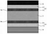
图1以截面图(且为局部视图)示意性地示出了根据本发明的在制造过程中的半导体器件(尤其是光伏电池)的一个实施例。附图中各材料层未按比例绘制。FIG. 1 schematically shows an embodiment of a semiconductor device (in particular a photovoltaic cell) according to the invention in a cross-sectional view (and a partial view) during manufacture. The layers of material in the figures are not drawn to scale.
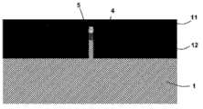
图2也以截面图且仍然为局部视图示出了在其制造结束时的该半导体器件。FIG. 2 also shows the semiconductor device at the end of its manufacture in a cross-sectional view and still in a partial view.
图3示出了该半导体器件在其制造结束时的背表面的示意图。FIG. 3 shows a schematic view of the back surface of the semiconductor device at the end of its manufacture.
图4示出了该器件的局部示意图,为对应于图3中的A-A线的纵向截面。FIG. 4 shows a partial schematic diagram of the device, which is a longitudinal section corresponding to line A-A in FIG. 3 .
具体实施方式Detailed ways
在下面的描述中,参考本发明的光伏应用,将更加详细而非限定地描述本发明。In the following description, the invention will be described in more detail without limitation with reference to photovoltaic applications of the invention.
参见图1,根据本发明的半导体器件可制造如下。Referring to FIG. 1, a semiconductor device according to the present invention can be fabricated as follows.
首先,提供具有前表面1a和背表面1b的晶体半导体基板1。优选地,晶体半导体基板1为晶体,尤其是晶片形式的单晶或多晶(优选单晶)硅基板(或晶片)。First, a
该基板可被n型或p型掺杂。因为n型掺杂基板的寿命较长,所以采用该基板特别有利。下面,采用n型掺杂基板作为示例。有利地,基板1不具有任何氧化物材料。The substrate can be doped n-type or p-type. The use of n-type doped substrates is particularly advantageous due to their longer lifetime. In the following, an n-type doped substrate is taken as an example. Advantageously, the
优选地,基板1具有足够的掺杂以具有在约0.1和1Ω.cm之间的电阻率。Preferably, the
在基板1的两侧上,也就是在其前表面1a和在其背表面1b上,分别施加前钝化层3和后钝化层2。On both sides of the
前钝化层3有利地包括与基板1接触的非晶本征氢化硅层6和在非晶本征氢化硅层6上设置的掺杂氢化非晶硅层7。当基板1为n型时,掺杂氢化非晶硅层7为n型掺杂;或者当基板1为p型时,它为p型掺杂。The
对称地,后钝化层2有利地包括与基板1接触的非晶本征氢化硅层4和在非晶本征氢化硅层4上设置的掺杂氢化非晶硅层5。优选地,掺杂氢化非晶硅层5为n型掺杂,而不论基板1的掺杂类型。Symmetrically, the
前钝化层3和后钝化层2以两个互补的方式实现钝化的任务:一方面,晶体基板的每个面1a、1b上的非晶硅的存在使得可以通过防止结合物(pendant)接合到表面上而使基板的表面缺陷不具有活性,这防止了电荷载流子在它们被收集前复合;另一方面,掺杂氢化非晶硅层5、7的存在使得可以分别产生前表面场和后表面场,以改善电荷载流子的收集。The
沉积两个本征氢化非晶硅层4、6和两个掺杂氢化非晶硅层5、7例如可通过等离子体增强化学气相沉积(PECVD)技术或通过低压化学气相沉积(LPCVD)技术来进行。上述层的每一个可覆盖基板1的整个表面。Depositing two intrinsic hydrogenated
抗反射层8有利地设置在前钝化层3上。该抗反射层包括电介质材料,优选为氢化非晶氮化硅。优选地,它延伸在前钝化层3的整个表面上。例如,它可通过PECVD或LPCVD技术沉积。抗反射层的主要作用是尽可能多地消除通过前侧到达器件的光的反射。抗反射层的折射系数例如可在2附近。可以采用纹理化的硅来改善光收集。An
在后钝化层2上,沉积金属层9。例如这可通过蒸发、喷涂或通过电化学沉积来实现。金属层9优选为铝基材料。根据图1所示的实施例,金属层9最初覆盖后钝化层2的整个表面;然后,一部分金属层9(通过蚀刻或另外的技术)被选择性去除,以获得第一金属化区域10以及与第一金属化区域10隔开的第二金属化区域11。On the rear passivation layer 2 a
优选地,第一金属化区域10和第二金属化区域11形成如图3所示的交叉梳状结构(interdigitated structure),也就是两个金属化区域10、11形成反向且互锁的梳状的结构。金属化区域10、11要收集各自的电荷载流子。交叉梳状结构能使器件实现特别简单的电连接。Preferably, the
作为选择,也可在后钝化层2的表面直接选择性地施加金属化区域10、11,从而直接获得所希望的(例如交叉梳状的)图案。为此,可以采用通过适当形状的掩模丝网印刷金属膏,或者采用通过掩模的蒸发或喷涂。Alternatively, the
根据上述的主要实施例,金属化区域10、11由一种且相同的材料(优选为铝基材料)制作:该实施例实际上是最简单的实施方式。然而,可以制备组成彼此不同的金属化区域10、11。在此情况下,至少第二金属化区域11优选为铝基材料。According to the main embodiment described above, the metallized
接下来,进行第二金属化区域11的激光退火(或激光烘烤)步骤。激光退火在于给第二金属化区域11施加激光脉冲,从而在非常短的时间使第二金属化区域11以及一定厚度的下层硅进行熔化/凝固循环。在熔化相期间,金属(尤其是铝)快速扩散进入液态硅中。在凝固工艺期间,硅再一次从下层固体硅外延;然后在熔化周期期间已经扩散的金属(尤其是铝)的原子(掺杂剂)在重构的晶体中位于取代位置。Next, a laser annealing (or laser baking) step of the
因此,并且参见图2,在激光退火结束时,第二金属化区域一方面包括表面部分11且另一方面包括内部部分12,表面部分11位于后钝化层3上且基本上对应于激光退火前的第二金属化区域,内部部分12通过后钝化层2且进入到基板1中,该内部部分12通过激光退火期间的原子(尤其是铝)扩散而获得。Thus, and referring to FIG. 2 , at the end of the laser annealing, the second metallization region comprises on the one hand a
因此,第二金属化区域的内部部分12包括基板1的一个区域,该区域位于第二金属化区域的表面部分11之下且被p+掺杂(也就是,该区域具有高浓度的p型掺杂剂,尤其是铝原子)。换言之,第二金属化区域的内部部分12因此在基板1中形成了一个区域,在该区域中电子受主的浓度比基板1的其它区域大,不论基板1是n型或p型。当基板1为n型时,p-n型结由此形成在基板1的由激光退火改性的区域和基板1的其它区域之间;当基板1为p型时,由此形成p-p+型结。Thus, the
激光退火期间凝固前沿的极高速度有利于方形分布的形成,并且使得可以实现比传统技术获得的激活率大的激活率。根据该技术,激光能量决定了基板1的如此掺杂的区域的厚度。在激光处理后,掺杂剂被电激活,掺杂分布几乎为方形并具有非常陡峭的侧部。The extremely high speed of the solidification front during laser annealing favors the formation of a square distribution and makes it possible to achieve activation rates greater than those obtained with conventional techniques. According to this technique, the laser energy determines the thickness of the thus doped regions of the
下面的文件提供了实施激光退火技术的示例:The following documents provide examples of implementing laser annealing techniques:
-Laser fired back contact for silicon cells,Tucci et al.,Thin solid films516:6767-6770(2008);-Laser fired back contact for silicon cells, Tucci et al., Thin solid films 516: 6767-6770 (2008);
-Laser fired contacts on amorphous silicon deposited by hot-wire CVDon crystalline silicon,Blanquéet al.,23rd European photovoltaic solar energyconference,1-5 September 2008,Valence(Espagne),p.1393-1396;-Laser fired contacts on amorphous silicon deposited by hot-wire CVDon crystalline silicon, Blanqué et al., 23rd European photovoltaic solar energy conference, 1-5 September 2008, Valence (Espagne), p.1393-1396;
-Bragg reflector and laser fired back contact in a-Si:H/c-Siheterostructure,Tucci et al.,Materials Science and Engineering B 159-160:48-52(2009).-Bragg reflector and laser fired back contact in a-Si: H/c-Siheterostructure, Tucci et al., Materials Science and Engineering B 159-160: 48-52 (2009).
典型地,可采用脉冲Nd-YAG激光器或者脉冲UV准分子激光器。通过示例的方式,可采用TEM00模式的1064nm的Nd-YAG调Q激光器(Q-switched laser),功率为300至900mW,脉冲持续时间为100ms,重复频率为1kHz。Typically, a pulsed Nd-YAG laser or a pulsed UV excimer laser can be used. By way of example, a 1064 nm Nd-YAG Q-switched laser (Q-switched laser) in TEM00 mode can be used with a power of 300 to 900 mW, a pulse duration of 100 ms, and a repetition rate of 1 kHz.
通常,激光器的功率和脉冲持续时间调整为所希望的退火深度及诱导掺杂的函数。激光的运动速度和频率被调整,以调整激光冲击之间的距离。Typically, laser power and pulse duration are adjusted as a function of the desired anneal depth and induced doping. The speed and frequency of laser movement are adjusted to adjust the distance between laser strikes.
当第二金属化区域的表面部分11具有条状图案时,如交叉梳状结构时的情况,沿着条状图案的激光冲击之间的距离(见图4)必须足够小,以便限制欧姆损耗且优化电荷收集。When the
在激光退火结束时:At the end of laser annealing:
-第一金属化区域10仍然仅位于后钝化层2的顶部,并且更确切地说仅位于n型掺杂氢化非晶硅层5的顶部。因此,该第一金属化区域10保证了n型接触,也就是说适合于收集电子。- The
-第二金属化区域已经转变成了p型接触,也就是说它适合于收集空穴。- The second metallization area has been transformed into a p-type contact, that is to say it is suitable for collecting holes.
通过示例的方式,如此获得的半导体器件的结构可为如下:By way of example, the structure of the semiconductor device thus obtained may be as follows:
-基板1:厚度在150和300μm之间。- Substrate 1: thickness between 150 and 300 μm.
-本征氢化非晶硅层4、6:厚度在1和10nm之间,尤其是在3和5nm之间。- Intrinsic hydrogenated
-掺杂氢化非晶硅层5、7:厚度在5和30nm之间,尤其是在5和15nm之间。- Doped hydrogenated
-抗反射层8:厚度在50和100nm之间。- Anti-reflection layer 8: thickness between 50 and 100 nm.
-第一金属化区域10和第二金属化区域的表面部分11:厚度在2和30μm之间,尤其是在2和10μm之间。- The
如果两个金属区域具有交叉梳状的形式,如这里所示的,则这些金属区域包括交替设置的平行条状图案。每个条可具有50至400μm的典型宽度,且尤其是50至200μm(例如约100μm)的典型宽度,并且两个条可隔开50至200μm(例如约100μm)的典型距离。If two metal regions have the form of an interdigitated comb, as shown here, these metal regions comprise a pattern of parallel strips arranged alternately. Each stripe may have a typical width of 50 to 400 μm, and in particular 50 to 200 μm (eg about 100 μm), and two stripes may be separated by a typical distance of 50 to 200 μm (eg about 100 μm).
由于掺杂非晶硅的存在,电荷载流子进入后钝化层2的扩散长度典型地为约20nm。因此,取决于后钝化层2的厚度电荷载流子可通过后钝化层2,但是在平行于基板1的背表面1a的方向上电荷载流子基本上不能通过后钝化层2。因此,实际上在两个各自的金属化区域之间没有短路的可能性。Due to the presence of doped amorphous silicon, the diffusion length of the charge carriers into the
上面的描述涉及通常用作光伏电池的半导体器件。这些器件的一个或多个可以以光伏电池模块的方式结合。例如,一定数量的光伏电池可串联和/或并联电连接,以便形成模块。The above description relates to semiconductor devices commonly used as photovoltaic cells. One or more of these devices may be combined in a photovoltaic cell module. For example, a number of photovoltaic cells may be electrically connected in series and/or in parallel to form a module.
模块可以以各种方法制造。例如,光伏电池可设置在玻璃片之间,或设置在玻璃片和透明树脂片之间,透明树脂片例如由乙烯/乙酸乙烯酯制成。如果所有的光伏电池的前表面沿相同的方向取向,则也可在后侧采用不透明的片(金属或陶瓷等)。也可将模块制作成在两个相对的面上接收光(对此例如参见文件US 6,667,435)。可提供密封树脂以密封模块的侧部,并且保护模块免受大气湿气的影响。也可提供各种树脂层以防止来自玻璃片的钠的不希望的扩散。Modules can be manufactured in various ways. For example, a photovoltaic cell may be disposed between sheets of glass, or between a sheet of glass and a sheet of transparent resin, for example made of ethylene/vinyl acetate. If the front surfaces of all photovoltaic cells are oriented in the same direction, opaque sheets (metal or ceramic, etc.) can also be used on the rear side. The module can also be made to receive light on two opposite faces (see for example document US 6,667,435 for this). A sealing resin is available to seal the sides of the module and protect the module from atmospheric moisture. Various resin layers may also be provided to prevent undesired diffusion of sodium from the glass sheet.
此外,模块通常包括各光伏电池端子处的静态转换装置。根据应用,这些装置可为直流-交流(DC/AC)转换装置和/或直流-直流(DC/DC)转换装置。静态转换装置适合于将光伏电池提供的电力传输为使外部应用(电池或电网等)充电。这些静态转换装置适合于降低传输电流以且提高传输电压。静态转换装置可与电子控制器结合。Furthermore, the modules typically include static conversion means at the terminals of each photovoltaic cell. Depending on the application, these devices may be direct current-alternating current (DC/AC) conversion devices and/or direct current-direct current (DC/DC) conversion devices. Static conversion devices are suitable for transferring electricity provided by photovoltaic cells to charge an external application (battery or grid, etc.). These static switching devices are suitable for reducing the transmission current and increasing the transmission voltage. Static switching devices can be combined with electronic controllers.
太阳能模块的制造细节(支撑元件、框架、电连接、封装等)已被本领域技术人员所熟知。The manufacturing details of solar modules (support elements, frame, electrical connections, encapsulation, etc.) are well known to those skilled in the art.
Claims (16)
Applications Claiming Priority (3)
| Application Number | Priority Date | Filing Date | Title |
|---|---|---|---|
| FR09/58922 | 2009-12-14 | ||
| FR0958922AFR2953999B1 (en) | 2009-12-14 | 2009-12-14 | PHOTOVOLTAIC CELL HETEROJUNCTION WITH REAR CONTACT |
| PCT/IB2010/055725WO2011073868A2 (en) | 2009-12-14 | 2010-12-10 | Rear-contact heterojunction photovoltaic cell |
Publications (1)
| Publication Number | Publication Date |
|---|---|
| CN102792455Atrue CN102792455A (en) | 2012-11-21 |
Family
ID=42713403
Family Applications (1)
| Application Number | Title | Priority Date | Filing Date |
|---|---|---|---|
| CN2010800638402APendingCN102792455A (en) | 2009-12-14 | 2010-12-10 | Rear-contact heterojunction photovoltaic cell |
Country Status (12)
| Country | Link |
|---|---|
| US (1) | US20120247539A1 (en) |
| EP (1) | EP2513978B1 (en) |
| JP (1) | JP2013513964A (en) |
| KR (2) | KR20170029652A (en) |
| CN (1) | CN102792455A (en) |
| AU (1) | AU2010331900B2 (en) |
| BR (1) | BR112012014143A8 (en) |
| CA (1) | CA2784491C (en) |
| FR (1) | FR2953999B1 (en) |
| RU (1) | RU2555212C2 (en) |
| WO (1) | WO2011073868A2 (en) |
| ZA (1) | ZA201204008B (en) |
Cited By (2)
| Publication number | Priority date | Publication date | Assignee | Title |
|---|---|---|---|---|
| CN103050553A (en)* | 2012-12-29 | 2013-04-17 | 中国科学院沈阳科学仪器股份有限公司 | Crystalline silicon solar cell with double-side passivation and preparing method thereof |
| CN114008798A (en)* | 2019-07-26 | 2022-02-01 | 迈尔博尔格(德国)有限公司 | Photovoltaic device and method of manufacturing the same |
Families Citing this family (12)
| Publication number | Priority date | Publication date | Assignee | Title |
|---|---|---|---|---|
| EP2690668A4 (en)* | 2011-03-25 | 2014-09-03 | Sanyo Electric Co | METHOD FOR PRODUCING PHOTOELECTRIC CONVERSION ELEMENT |
| WO2012132995A1 (en)* | 2011-03-25 | 2012-10-04 | 三洋電機株式会社 | Method for producing photoelectric conversion element |
| FI20116217A7 (en)* | 2011-12-02 | 2013-06-03 | Beneq Oy | An n-type silicon photovoltaic cell structure |
| US9202959B2 (en) | 2012-09-25 | 2015-12-01 | International Business Machines Corporation | Embedded junction in hetero-structured back-surface field for photovoltaic devices |
| US9640699B2 (en) | 2013-02-08 | 2017-05-02 | International Business Machines Corporation | Interdigitated back contact heterojunction photovoltaic device |
| US9859455B2 (en) | 2013-02-08 | 2018-01-02 | International Business Machines Corporation | Interdigitated back contact heterojunction photovoltaic device with a floating junction front surface field |
| CN103178135B (en)* | 2013-02-26 | 2015-10-14 | 友达光电股份有限公司 | Solar cell and manufacturing method thereof |
| CN103746005B (en)* | 2014-01-17 | 2016-08-17 | 宁波富星太阳能有限公司 | Double-layer silicon nitride anti-reflection coating |
| FR3040822B1 (en)* | 2015-09-07 | 2018-02-23 | Ecole Polytechnique | METHOD FOR MANUFACTURING ELECTRONIC JUNCTION DEVICE AND DEVICE THEREOF |
| KR102480841B1 (en) | 2021-01-21 | 2022-12-23 | 경북대학교 산학협력단 | Photoelectrochemical cell and manufacturing method thereof |
| CN113963836A (en)* | 2021-08-29 | 2022-01-21 | 东华理工大学 | Nuclear battery based on silicon carbide PN junction type beta radiation volt effect |
| DE102023135277A1 (en)* | 2023-12-15 | 2025-06-18 | Ce Cell Engineering Gmbh | Wafer solar cell and method for producing such a wafer solar cell |
Citations (4)
| Publication number | Priority date | Publication date | Assignee | Title |
|---|---|---|---|---|
| US5641362A (en)* | 1995-11-22 | 1997-06-24 | Ebara Solar, Inc. | Structure and fabrication process for an aluminum alloy junction self-aligned back contact silicon solar cell |
| CN101097969A (en)* | 2006-06-30 | 2008-01-02 | 通用电气公司 | Optoelectronic devices including all back contact structures and related processing |
| CN101414648A (en)* | 2007-10-17 | 2009-04-22 | 财团法人工业技术研究院 | Method for rapid hydrogen passivation of crystalline silicon solar cells |
| US20090223562A1 (en)* | 2006-10-27 | 2009-09-10 | Kyocera Corporation | Solar Cell Element Manufacturing Method and Solar Cell Element |
Family Cites Families (20)
| Publication number | Priority date | Publication date | Assignee | Title |
|---|---|---|---|---|
| US4839312A (en)* | 1978-03-16 | 1989-06-13 | Energy Conversion Devices, Inc. | Fluorinated precursors from which to fabricate amorphous semiconductor material |
| US4703553A (en)* | 1986-06-16 | 1987-11-03 | Spectrolab, Inc. | Drive through doping process for manufacturing low back surface recombination solar cells |
| US5538564A (en)* | 1994-03-18 | 1996-07-23 | Regents Of The University Of California | Three dimensional amorphous silicon/microcrystalline silicon solar cells |
| US5571339A (en)* | 1995-04-17 | 1996-11-05 | The Ohio State Univ. Research Found | Hydrogen passivated heteroepitaxial III-V photovoltaic devices grown on lattice-mismatched substrates, and process |
| US6262359B1 (en)* | 1999-03-17 | 2001-07-17 | Ebara Solar, Inc. | Aluminum alloy back junction solar cell and a process for fabrication thereof |
| JP2001291881A (en) | 2000-01-31 | 2001-10-19 | Sanyo Electric Co Ltd | Solar cell module |
| DE10046170A1 (en)* | 2000-09-19 | 2002-04-04 | Fraunhofer Ges Forschung | Method for producing a semiconductor-metal contact through a dielectric layer |
| JP2003298078A (en) | 2002-03-29 | 2003-10-17 | Ebara Corp | Photovoltaic element |
| US7335835B2 (en)* | 2002-11-08 | 2008-02-26 | The Boeing Company | Solar cell structure with by-pass diode and wrapped front-side diode interconnection |
| DE102004050269A1 (en) | 2004-10-14 | 2006-04-20 | Institut Für Solarenergieforschung Gmbh | Process for the contact separation of electrically conductive layers on back-contacted solar cells and solar cell |
| FR2880989B1 (en) | 2005-01-20 | 2007-03-09 | Commissariat Energie Atomique | SEMICONDUCTOR DEVICE WITH HETEROJUNCTIONS AND INTERDIGITAL STRUCTURE |
| US20070137692A1 (en) | 2005-12-16 | 2007-06-21 | Bp Corporation North America Inc. | Back-Contact Photovoltaic Cells |
| US20070169808A1 (en) | 2006-01-26 | 2007-07-26 | Kherani Nazir P | Solar cell |
| US7737357B2 (en) | 2006-05-04 | 2010-06-15 | Sunpower Corporation | Solar cell having doped semiconductor heterojunction contacts |
| FR2906403B1 (en)* | 2006-09-21 | 2008-12-19 | Commissariat Energie Atomique | METHOD FOR RECLAIMING PHOTOVOLTAIC CELLS |
| DE102006046726A1 (en)* | 2006-10-02 | 2008-04-03 | Fraunhofer-Gesellschaft zur Förderung der angewandten Forschung e.V. | Silicon-based solar cell comprises front-end contacts that are placed on a front-end doped surface layer and a passivation layer with backside contacts that is placed on the backside doped layer |
| RU2331139C1 (en)* | 2007-02-28 | 2008-08-10 | Российская Академия сельскохозяйственных наук Государственное научное учреждение Всероссийский научно-исследовательский институт электрификации сельского хозяйства (ГНУ ВИЭСХ РОССЕЛЬХОЗАКАДЕМИИ) | Photo-electric converter and method of its production (versions) |
| JP2010527146A (en)* | 2007-05-07 | 2010-08-05 | ジョージア テック リサーチ コーポレイション | Formation of high quality back contact with screen printed local back surface field |
| US20100218821A1 (en)* | 2009-03-02 | 2010-09-02 | Sunyoung Kim | Solar cell and method for manufacturing the same |
| TW201140866A (en)* | 2009-12-07 | 2011-11-16 | Applied Materials Inc | Method of cleaning and forming a negatively charged passivation layer over a doped region |
- 2009
- 2009-12-14FRFR0958922Apatent/FR2953999B1/enactiveActive
- 2010
- 2010-12-10KRKR1020177006259Apatent/KR20170029652A/ennot_activeCeased
- 2010-12-10WOPCT/IB2010/055725patent/WO2011073868A2/enactiveApplication Filing
- 2010-12-10RURU2012129993/28Apatent/RU2555212C2/enactive
- 2010-12-10JPJP2012543955Apatent/JP2013513964A/enactivePending
- 2010-12-10CNCN2010800638402Apatent/CN102792455A/enactivePending
- 2010-12-10BRBR112012014143Apatent/BR112012014143A8/enactiveSearch and Examination
- 2010-12-10AUAU2010331900Apatent/AU2010331900B2/enactiveActive
- 2010-12-10KRKR1020127018378Apatent/KR20120094131A/ennot_activeCeased
- 2010-12-10EPEP10809184.4Apatent/EP2513978B1/enactiveActive
- 2010-12-10CACA2784491Apatent/CA2784491C/enactiveActive
- 2010-12-10USUS13/515,657patent/US20120247539A1/ennot_activeAbandoned
- 2012
- 2012-06-01ZAZA201204008Apatent/ZA201204008B/enunknown
Patent Citations (4)
| Publication number | Priority date | Publication date | Assignee | Title |
|---|---|---|---|---|
| US5641362A (en)* | 1995-11-22 | 1997-06-24 | Ebara Solar, Inc. | Structure and fabrication process for an aluminum alloy junction self-aligned back contact silicon solar cell |
| CN101097969A (en)* | 2006-06-30 | 2008-01-02 | 通用电气公司 | Optoelectronic devices including all back contact structures and related processing |
| US20090223562A1 (en)* | 2006-10-27 | 2009-09-10 | Kyocera Corporation | Solar Cell Element Manufacturing Method and Solar Cell Element |
| CN101414648A (en)* | 2007-10-17 | 2009-04-22 | 财团法人工业技术研究院 | Method for rapid hydrogen passivation of crystalline silicon solar cells |
Cited By (4)
| Publication number | Priority date | Publication date | Assignee | Title |
|---|---|---|---|---|
| CN103050553A (en)* | 2012-12-29 | 2013-04-17 | 中国科学院沈阳科学仪器股份有限公司 | Crystalline silicon solar cell with double-side passivation and preparing method thereof |
| CN103050553B (en)* | 2012-12-29 | 2015-06-24 | 中国科学院沈阳科学仪器股份有限公司 | Crystalline silicon solar cell with double-side passivation and preparing method thereof |
| CN114008798A (en)* | 2019-07-26 | 2022-02-01 | 迈尔博尔格(德国)有限公司 | Photovoltaic device and method of manufacturing the same |
| CN114008798B (en)* | 2019-07-26 | 2024-02-13 | 迈尔博尔格(德国)有限公司 | Photovoltaic device and method for manufacturing the same |
Also Published As
| Publication number | Publication date |
|---|---|
| BR112012014143A2 (en) | 2016-08-16 |
| KR20170029652A (en) | 2017-03-15 |
| JP2013513964A (en) | 2013-04-22 |
| EP2513978A2 (en) | 2012-10-24 |
| ZA201204008B (en) | 2020-11-25 |
| RU2555212C2 (en) | 2015-07-10 |
| US20120247539A1 (en) | 2012-10-04 |
| BR112012014143A8 (en) | 2017-12-26 |
| WO2011073868A3 (en) | 2011-09-01 |
| AU2010331900B2 (en) | 2015-09-10 |
| WO2011073868A2 (en) | 2011-06-23 |
| AU2010331900A1 (en) | 2012-07-19 |
| KR20120094131A (en) | 2012-08-23 |
| RU2012129993A (en) | 2014-01-27 |
| CA2784491C (en) | 2018-02-20 |
| CA2784491A1 (en) | 2011-06-23 |
| EP2513978B1 (en) | 2015-03-25 |
| FR2953999B1 (en) | 2012-01-20 |
| FR2953999A1 (en) | 2011-06-17 |
Similar Documents
| Publication | Publication Date | Title |
|---|---|---|
| CA2784491C (en) | Rear-contact heterojunction photovoltaic cell | |
| JP5328363B2 (en) | Method for manufacturing solar cell element and solar cell element | |
| JP5025184B2 (en) | Solar cell element, solar cell module using the same, and manufacturing method thereof | |
| CN102763225B (en) | High-efficiency photovoltaic back-junction back-contact solar cell structure and fabrication method using semiconductor wafer | |
| JP4334455B2 (en) | Solar cell module | |
| TW201924073A (en) | Interdigitated back contact solar cell with p-type conductivity | |
| JP2016111357A (en) | Solar battery, solar battery module, and method of manufacturing solar battery | |
| JP2013239476A (en) | Photovoltaic device and method of manufacturing the same, and photovoltaic module | |
| CN103875082B (en) | The manufacture method of photovoltaic devices and photovoltaic devices | |
| KR101597532B1 (en) | The Manufacturing Method of Back Contact Solar Cells | |
| KR101729745B1 (en) | Solar cell and manufacturing method thereof | |
| JP2013048126A (en) | Photovoltaic device and manufacturing method thereof | |
| US8283199B2 (en) | Solar cell patterning and metallization | |
| JP2015146335A (en) | Photovoltaic element and manufacturing method thereof | |
| JP5645734B2 (en) | Solar cell element | |
| JP2005260157A (en) | Solar cell and solar cell module | |
| JP4467337B2 (en) | Solar cell module | |
| JP5501549B2 (en) | Photoelectric conversion element and photoelectric conversion module composed thereof | |
| US20190081186A1 (en) | Solar cell element and solar cell module | |
| JP5029921B2 (en) | Method for manufacturing solar battery cell | |
| KR101199649B1 (en) | Localized Emitter Solar Cell and Method for Manufacturing Thereof | |
| KR101114198B1 (en) | Localized emitter solar cell and method for manufacturing thereof | |
| US20110155225A1 (en) | Back contact solar cells having exposed vias | |
| KR101588456B1 (en) | Solar cell and manufacturing mehtod of the same | |
| CN115425111A (en) | Manufacturing method of doping structure, solar cell assembly and solar cell system |
Legal Events
| Date | Code | Title | Description |
|---|---|---|---|
| C06 | Publication | ||
| PB01 | Publication | ||
| C10 | Entry into substantive examination | ||
| SE01 | Entry into force of request for substantive examination | ||
| ASS | Succession or assignment of patent right | Owner name:TOTAL RAFFINAGE MARKETING Free format text:FORMER OWNER: TOTAL S.A. Effective date:20140418 | |
| C41 | Transfer of patent application or patent right or utility model | ||
| C53 | Correction of patent of invention or patent application | ||
| CB02 | Change of applicant information | Address after:French pitot Applicant after:TOTAL MARKETING SERVICES Applicant after:CENTRE NATIONAL DE LA RECHERCHE SCIENTIFIQUE Applicant after:ECOLE POLYTECHNIQUE Address before:French pitot Applicant before:Total Raffinage Marketing Applicant before:CENTRE NATIONAL DE LA RECHERCHE SCIENTIFIQUE Applicant before:ECOLE POLYTECHNIQUE | |
| COR | Change of bibliographic data | Free format text:CORRECT: APPLICANT; FROM: TOTAL RAFFINAGE MARKETING TO: TOTAL SALES SERVICE CORP. | |
| TA01 | Transfer of patent application right | Effective date of registration:20140418 Address after:French pitot Applicant after:TOTAL RAFFINAGE MARKETING Applicant after:CENTRE NATIONAL DE LA RECHERCHE SCIENTIFIQUE Applicant after:ECOLE POLYTECHNIQUE Address before:Kolb tile Applicant before:Total S.A. Applicant before:CENTRE NATIONAL DE LA RECHERCHE SCIENTIFIQUE Applicant before:ECOLE POLYTECHNIQUE | |
| WD01 | Invention patent application deemed withdrawn after publication | ||
| WD01 | Invention patent application deemed withdrawn after publication | Application publication date:20121121 |