CN102790016A - Bump structure and manufacturing process - Google Patents
Bump structure and manufacturing processDownload PDFInfo
- Publication number
- CN102790016A CN102790016ACN2011101347294ACN201110134729ACN102790016ACN 102790016 ACN102790016 ACN 102790016ACN 2011101347294 ACN2011101347294 ACN 2011101347294ACN 201110134729 ACN201110134729 ACN 201110134729ACN 102790016 ACN102790016 ACN 102790016A
- Authority
- CN
- China
- Prior art keywords
- groove
- engaging groove
- metal layer
- block
- layer
- Prior art date
- Legal status (The legal status is an assumption and is not a legal conclusion. Google has not performed a legal analysis and makes no representation as to the accuracy of the status listed.)
- Granted
Links
- 238000004519manufacturing processMethods0.000titleclaimsabstractdescription26
- 229910052751metalInorganic materials0.000claimsabstractdescription86
- 239000002184metalSubstances0.000claimsabstractdescription86
- 239000010410layerSubstances0.000claimsdescription151
- 239000011241protective layerSubstances0.000claimsdescription28
- 229920002120photoresistant polymerPolymers0.000claimsdescription13
- 238000011161developmentMethods0.000claimsdescription3
- 229920002521macromoleculePolymers0.000claims27
- 229920000642polymerPolymers0.000abstractdescription133
- 238000003466weldingMethods0.000description18
- 239000010931goldSubstances0.000description15
- PCHJSUWPFVWCPO-UHFFFAOYSA-NgoldChemical compound[Au]PCHJSUWPFVWCPO-UHFFFAOYSA-N0.000description13
- 229910052737goldInorganic materials0.000description13
- 239000000758substrateSubstances0.000description8
- 230000005496eutecticsEffects0.000description6
- 239000000463materialSubstances0.000description6
- 239000011521glassSubstances0.000description5
- 238000005272metallurgyMethods0.000description5
- 238000000034methodMethods0.000description4
- XUIMIQQOPSSXEZ-UHFFFAOYSA-NSiliconChemical compound[Si]XUIMIQQOPSSXEZ-UHFFFAOYSA-N0.000description3
- 230000007547defectEffects0.000description3
- 238000012986modificationMethods0.000description3
- 230000004048modificationEffects0.000description3
- 229910052710siliconInorganic materials0.000description3
- 239000010703siliconSubstances0.000description3
- 238000013461designMethods0.000description2
- 230000000694effectsEffects0.000description2
- 238000004806packaging method and processMethods0.000description2
- 229910000679solderInorganic materials0.000description2
- 230000009286beneficial effectEffects0.000description1
- 238000009713electroplatingMethods0.000description1
- 238000005516engineering processMethods0.000description1
- 239000002245particleSubstances0.000description1
- 238000007747platingMethods0.000description1
- 230000008092positive effectEffects0.000description1
- 230000000750progressive effectEffects0.000description1
- 238000012827research and developmentMethods0.000description1
- MAKDTFFYCIMFQP-UHFFFAOYSA-Ntitanium tungstenChemical compound[Ti].[W]MAKDTFFYCIMFQP-UHFFFAOYSA-N0.000description1
Images


Classifications
- H—ELECTRICITY
- H01—ELECTRIC ELEMENTS
- H01L—SEMICONDUCTOR DEVICES NOT COVERED BY CLASS H10
- H01L24/00—Arrangements for connecting or disconnecting semiconductor or solid-state bodies; Methods or apparatus related thereto
- H01L24/01—Means for bonding being attached to, or being formed on, the surface to be connected, e.g. chip-to-package, die-attach, "first-level" interconnects; Manufacturing methods related thereto
- H01L24/10—Bump connectors ; Manufacturing methods related thereto
- H01L24/11—Manufacturing methods
- H—ELECTRICITY
- H01—ELECTRIC ELEMENTS
- H01L—SEMICONDUCTOR DEVICES NOT COVERED BY CLASS H10
- H01L2224/00—Indexing scheme for arrangements for connecting or disconnecting semiconductor or solid-state bodies and methods related thereto as covered by H01L24/00
- H01L2224/01—Means for bonding being attached to, or being formed on, the surface to be connected, e.g. chip-to-package, die-attach, "first-level" interconnects; Manufacturing methods related thereto
- H01L2224/10—Bump connectors; Manufacturing methods related thereto
- H01L2224/11—Manufacturing methods
- H—ELECTRICITY
- H01—ELECTRIC ELEMENTS
- H01L—SEMICONDUCTOR DEVICES NOT COVERED BY CLASS H10
- H01L2924/00—Indexing scheme for arrangements or methods for connecting or disconnecting semiconductor or solid-state bodies as covered by H01L24/00
- H01L2924/013—Alloys
- H01L2924/0132—Binary Alloys
- H01L2924/01322—Eutectic Alloys, i.e. obtained by a liquid transforming into two solid phases
- H—ELECTRICITY
- H01—ELECTRIC ELEMENTS
- H01L—SEMICONDUCTOR DEVICES NOT COVERED BY CLASS H10
- H01L2924/00—Indexing scheme for arrangements or methods for connecting or disconnecting semiconductor or solid-state bodies as covered by H01L24/00
- H01L2924/15—Details of package parts other than the semiconductor or other solid state devices to be connected
- H01L2924/151—Die mounting substrate
- H01L2924/156—Material
- H01L2924/15786—Material with a principal constituent of the material being a non metallic, non metalloid inorganic material
- H01L2924/15788—Glasses, e.g. amorphous oxides, nitrides or fluorides
Landscapes
- Engineering & Computer Science (AREA)
- Manufacturing & Machinery (AREA)
- Computer Hardware Design (AREA)
- Microelectronics & Electronic Packaging (AREA)
- Power Engineering (AREA)
- Manufacturing Of Electrical Connectors (AREA)
Abstract
Description
Translated fromChinese技术领域technical field
本发明涉及一种凸块结构及制造工艺,特别是涉及一种可提高共晶可靠度的凸块结构及制造工艺。The invention relates to a bump structure and a manufacturing process, in particular to a bump structure and a manufacturing process that can improve the reliability of eutectic.
背景技术Background technique
现有习知的金凸块结构10形成于硅基板20上,该硅基板20具有多个焊垫21及一保护层22,该保护层22形成有多个开口23,所述开口23显露出所述焊垫21,该凸块结构10包含一凸块下金属层11以及一金凸块层12,该凸块下金属层11形成于所述焊垫21上,该金凸块层12形成于该凸块下金属层11上,因此当该金凸块结构10与另一电子元件的接点(如连接垫或引脚)共晶接合时,该金凸块结构10与该接点的接触面积并不大,相对地影响了该金凸块结构10与该接点的共晶可靠度,并且在该接点被触压结合于该金凸块结构10时,该接点会有偏移的情况,而造成相邻的接点接触而产生短路的情形,此外由于该金凸块结构10由该金凸块层12所构成,因此其生产成本较高。The conventional
由此可见,上述现有的凸块结构及制造工艺在产品结构、制造方法与使用上,显然仍存在有不便与缺陷,而亟待加以进一步改进。为了解决上述存在的问题,相关厂商莫不费尽心思来谋求解决之道,但长久以来一直未见适用的设计被发展完成,而一般产品及方法又没有适切的结构及方法能够解决上述问题,此显然是相关业者急欲解决的问题。因此如何能创设一种新的凸块结构及制造工艺,实属当前重要研发课题之一,亦成为当前业界极需改进的目标。It can be seen that the above-mentioned existing bump structure and manufacturing process obviously still have inconveniences and defects in terms of product structure, manufacturing method and use, and need to be further improved. In order to solve the above-mentioned problems, the relevant manufacturers have tried their best to find a solution, but no suitable design has been developed for a long time, and there is no suitable structure and method for general products and methods to solve the above-mentioned problems. This is obviously a problem that relevant industry players are eager to solve. Therefore, how to create a new bump structure and manufacturing process is one of the current important research and development topics, and has also become a goal that the industry needs to improve.
发明内容Contents of the invention
本发明的主要目的在于,克服现有的凸块结构存在的缺陷,而提供一种新型结构的凸块结构,所要解决的技术问题是提供一种凸块结构,其设置于一载板上,该载板具有多个焊垫及一保护层,该保护层具有多个开口,所述开口显露出所述焊垫,该凸块结构与各该焊垫电性连接,该凸块结构包含有一第一高分子块体、一第二高分子块体、一第一沟槽、一凸块下金属层及一接合金属层,其中该第一高分子块体及第二高分子块体分别为一独立的块体,且该第一高分子块体及该第二高分子块体位于该第一沟槽的二侧,该第一沟槽显露出该焊垫,该第一高分子块体及第二高分子块体其设置于该焊垫及该保护层上,该第一高分子块体具有一第一上表面及一凹设于该第一上表面的第一接合槽,该第二高分子块体具有一第二上表面及一凹设于该第二上表面的第二接合槽,其中该第一高分子块体的该第一接合槽及该第二高分子块体的该第二接合槽连通该第一沟槽,该凸块下金属层(UBM)覆盖该第一高分子块体、该第二高分子块体及该焊垫,且该凸块下金属层形成有一第二沟槽、一第三接合槽及一第四接合槽,该第三接合槽及该第四接合槽连通该第二沟槽,该接合金属层覆盖该凸块下金属层,并形成有一第三沟槽、一第五接合槽及一第六接合槽,该第五接合槽及该第六接合槽连通该第三沟槽,其中该凸块下金属层的该第二沟槽位于该第一沟槽与该接合金属层的该第三沟槽之间,该凸块下金属层的该第三接合槽位于该第一高分子块体的该第一接合槽与该接合金属层的该第五接合槽之间,该凸块下金属层的第四接合槽位于该第二高分子块体的该第二接合槽与该接合金属层的该第六接合槽之间,非常适于实用。The main purpose of the present invention is to overcome the defects of the existing bump structure and provide a new bump structure. The technical problem to be solved is to provide a bump structure, which is arranged on a carrier board. The carrier board has a plurality of welding pads and a protection layer, the protection layer has a plurality of openings, the openings expose the welding pads, the bump structure is electrically connected to each of the welding pads, and the bump structure includes a a first polymer block, a second polymer block, a first groove, an under bump metal layer and a bonding metal layer, wherein the first polymer block and the second polymer block are respectively An independent block, and the first polymer block and the second polymer block are located on two sides of the first groove, the first groove exposes the pad, and the first polymer block and a second polymer block which is disposed on the pad and the protection layer, the first polymer block has a first upper surface and a first bonding groove recessed on the first upper surface, the first The two polymer blocks have a second upper surface and a second joint groove recessed on the second upper surface, wherein the first joint groove of the first polymer block and the second joint groove of the second polymer block The second bonding groove communicates with the first groove, the under bump metallurgy (UBM) covers the first polymer block, the second polymer block and the pad, and the UBM layer forms There is a second groove, a third bonding groove and a fourth bonding groove, the third bonding groove and the fourth bonding groove communicate with the second groove, the bonding metal layer covers the UBM layer, and forms There is a third groove, a fifth bonding groove and a sixth bonding groove, the fifth bonding groove and the sixth bonding groove communicate with the third groove, wherein the second groove of the UBM layer is located Between the first groove and the third groove of the bonding metal layer, the third bonding groove of the UBM layer is located between the first bonding groove of the first polymer block and the bonding metal layer Between the fifth bonding groove of the UBM layer, the fourth bonding groove of the UBM layer is located between the second bonding groove of the second polymer block and the sixth bonding groove of the bonding metal layer, which is very suitable practical.
本发明的另一目的在于,克服现有的凸块制造工艺存在的缺陷,而提供一种新的凸块结构及制造工艺,所要解决的技术问题是提供一种凸块制造工艺,包含下列步骤,首先,提供一载板,其具有多个焊垫及一保护层,该保护层具有多个开口,所述开口显露出所述焊垫。之后,在该载板上形成一高分子层,该高分子层覆盖该保护层及所述焊垫。接着,提供一第一光罩并进行第一次曝光步骤。之后,移除该第一光罩并进行第一次显影步骤,以使该高分子层形成有多个高分子凸块,且每一高分子凸块对应一焊垫,各该高分子凸块包含有一第一高分子块体、一第二高分子块体及一第一沟槽,该第一高分子块体及该第二高分子块体分别为一独立的块体,且该第一高分子块体及该第二高分子块体位于该第一沟槽的二侧,该第一沟槽显露出该焊垫,且该第一高分子块体及该第二高分子块体设置于该焊垫及该保护层上,该第一高分子块体具有一第一上表面及一凹设于该第一上表面的第一接合槽,该第二高分子块体具有一第二上表面及一凹设于该第二上表面的第二接合槽,其中该第一高分子块体的该第一接合槽及该第二高分子块体的该第二接合槽连通该第一沟槽。接着,固化所述高分子凸块。之后,在该载板上形成一凸块下金属层(UBM),该凸块下金属层覆盖该保护层、该焊垫、该第一高分子块体及该第二高分子块体,其中该凸块下金属层形成有一第二沟槽、一第三接合槽及一第四接合槽,该第三接合槽及该第四接合槽连通该第二沟槽,该第二沟槽位于该第一沟槽上方,该第三接合槽位于该第一接合槽上方,该第四接合槽位于该第二接合槽上方。接着,在该凸块下金属层(UBM)上形成一光刻胶。之后,提供一第二光罩并进行第二次曝光步骤。接着,移除该第二光罩并进行第二次显影步骤,以使该光刻胶形成有多个开口,各该开口对应各该高分子凸块,且各该开口并显露出位在各该开口中的该凸块下金属层。之后,在所述开口中形成一接合金属层,该接合金属层覆盖被所述开口显露的该凸块下金属层,其中该接合金属层形成有一第三沟槽、一第五接合槽及一第六接合槽,该第五接合槽及该第六接合槽连通该第三沟槽,该第三沟槽位于该第二沟槽上方,该第五接合槽位于该第三接合槽上方,该第六接合槽位于该第四接合槽上方。接着,移除该光刻胶,以显露未被该接合金属层覆盖的该凸块下金属层。最后,移除未被该接合金属层覆盖的该凸块下金属层,以使该凸块下金属层仅覆盖该焊垫、该第一高分子块体及该第二高分子块体,从而更加适于实用。Another object of the present invention is to overcome the defects in the existing bump manufacturing process and provide a new bump structure and manufacturing process. The technical problem to be solved is to provide a bump manufacturing process, which includes the following steps , firstly, a carrier board is provided, which has a plurality of welding pads and a protection layer, and the protection layer has a plurality of openings, and the openings expose the welding pads. Afterwards, a polymer layer is formed on the carrier board, and the polymer layer covers the protection layer and the welding pad. Next, a first photomask is provided and a first exposure step is performed. Afterwards, remove the first photomask and carry out the first developing step, so that the polymer layer is formed with a plurality of polymer bumps, and each polymer bump corresponds to a welding pad, each of the polymer bumps Comprising a first polymer block, a second polymer block and a first groove, the first polymer block and the second polymer block are respectively an independent block, and the first The polymer block and the second polymer block are located on both sides of the first groove, the first groove exposes the pad, and the first polymer block and the second polymer block are set On the pad and the protective layer, the first polymer block has a first upper surface and a first bonding groove recessed on the first upper surface, and the second polymer block has a second an upper surface and a second joint groove recessed on the second upper surface, wherein the first joint groove of the first polymer block and the second joint groove of the second polymer block communicate with the first groove. Next, curing the polymer bumps. Afterwards, an under-bump metallurgy (UBM) is formed on the carrier, the under-bump metal layer covers the protection layer, the pad, the first polymer block and the second polymer block, wherein The UBM layer is formed with a second groove, a third bonding groove and a fourth bonding groove, the third bonding groove and the fourth bonding groove communicate with the second groove, and the second groove is located in the Above the first groove, the third engaging groove is located above the first engaging groove, and the fourth engaging groove is located above the second engaging groove. Next, a photoresist is formed on the UBM layer. Afterwards, a second photomask is provided and a second exposure step is performed. Then, remove the second photomask and perform a second developing step, so that the photoresist is formed with a plurality of openings, each of which corresponds to each of the polymer bumps, and each of the openings exposes the position at each The UBM layer in the opening. After that, a bonding metal layer is formed in the opening, the bonding metal layer covers the UBM layer exposed by the opening, wherein the bonding metal layer is formed with a third groove, a fifth bonding groove and a The sixth engaging groove, the fifth engaging groove and the sixth engaging groove communicate with the third groove, the third groove is located above the second groove, the fifth engaging groove is located above the third engaging groove, the The sixth engaging groove is located above the fourth engaging groove. Next, the photoresist is removed to expose the UBM layer not covered by the bonding metal layer. Finally, removing the UBM layer not covered by the bonding metal layer, so that the UBM layer only covers the pad, the first polymer block and the second polymer block, thereby more practical.
本发明的目的及解决其技术问题是采用以下技术方案来实现的。依据本发明提出的凸块结构,其设置于一载板上,该载板具有多个焊垫及一保护层,该保护层具有多个开口,所述开口显露出所述焊垫,该凸块结构与各该焊垫电性连接,该凸块结构包含有:一第一高分子块体,为一独立的块体,其设置于该焊垫及该保护层上,该第一高分子块体具有一第一上表面及一凹设于该第一上表面的第一接合槽;一第二高分子块体,为一独立的块体,其设置于该焊垫及该保护层上,该第二高分子块体具有一第二上表面及一凹设于该第二上表面的第二接合槽;一第一沟槽,其位于该第一高分子块体及该第二高分子块体之间,该第一沟槽显露出该焊垫,该第一高分子块体的该第一接合槽及该第二高分子块体的该第二接合槽连通该第一沟槽;一凸块下金属层(UBM),其覆盖该焊垫、该第一高分子块体及该第二高分子块体,其中该凸块下金属层形成有一第二沟槽、一第三接合槽及一第四接合槽;以及一接合金属层,其覆盖该凸块下金属层,并形成有一第三沟槽、一第五接合槽及一第六接合槽,该第五接合槽及该第六接合槽连通该第三沟槽,其中该凸块下金属层的该第二沟槽位于该第一沟槽与该接合金属层的该第三沟槽之间,该凸块下金属层的该第三接合槽位于该第一高分子块体的该第一接合槽与该接合金属层的该第五接合槽之间,该凸块下金属层的第四接合槽位于该第二高分子块体的该第二接合槽与该接合金属层的该第六接合槽之间。The purpose of the present invention and the solution to its technical problems are achieved by adopting the following technical solutions. According to the bump structure proposed by the present invention, it is arranged on a carrier board, the carrier board has a plurality of welding pads and a protective layer, the protective layer has a plurality of openings, the openings expose the welding pads, the bump The block structure is electrically connected to each of the pads, and the bump structure includes: a first polymer block, which is an independent block, which is arranged on the pad and the protective layer. The first polymer block The block has a first upper surface and a first bonding groove recessed on the first upper surface; a second polymer block, which is an independent block, is arranged on the pad and the protective layer , the second polymer block has a second upper surface and a second engagement groove recessed on the second upper surface; a first groove is located between the first polymer block and the second high polymer block Between the molecular blocks, the first groove exposes the pad, the first bonding groove of the first polymer block and the second bonding groove of the second polymer block communicate with the first groove ; An under bump metallurgy (UBM), which covers the pad, the first polymer block and the second polymer block, wherein the UBM layer is formed with a second trench, a third a bonding groove and a fourth bonding groove; and a bonding metal layer covering the UBM layer and forming a third groove, a fifth bonding groove and a sixth bonding groove, the fifth bonding groove and The sixth bonding groove communicates with the third groove, wherein the second groove of the UBM layer is located between the first groove and the third groove of the bonding metal layer, and the UBM The third bonding groove of the layer is located between the first bonding groove of the first polymer block and the fifth bonding groove of the bonding metal layer, and the fourth bonding groove of the UBM layer is located in the second Between the second bonding groove of the polymer block and the sixth bonding groove of the bonding metal layer.
本发明的目的及解决其技术问题还可采用以下技术措施进一步实现。The purpose of the present invention and its technical problems can also be further realized by adopting the following technical measures.
前述的凸块结构,其中所述的该第三沟槽、该第五接合槽及该第六接合槽为“+”状。In the aforementioned bump structure, the third groove, the fifth engaging groove, and the sixth engaging groove are in a "+" shape.
前述的凸块结构,其中所述的该第三沟槽具有一第一宽度,该第五接合槽具有一第二宽度,该第一宽度大于该第二宽度。In the aforementioned bump structure, the third groove has a first width, the fifth engaging groove has a second width, and the first width is greater than the second width.
前述的凸块结构,其中所述的该第六接合槽具有一第三宽度,该第一宽度大于该第三宽度。In the aforementioned bump structure, the sixth engagement groove has a third width, and the first width is greater than the third width.
本发明的目的及解决其技术问题还采用以下技术方案来实现。依据本发明提出的凸块制造工艺,其包括以下步骤:提供一载板,其具有多个焊垫及一保护层,该保护层具有多个开口,所述开口显露出所述焊垫;在该载板上形成一高分子层,该高分子层覆盖该保护层及所述焊垫;提供一第一光罩并进行第一次曝光步骤;移除该第一光罩并进行第一次显影步骤,以使该高分子层形成有多个高分子凸块,且每一高分子凸块对应一焊垫,各该高分子凸块包含有:一第一高分子块体,为一独立的块体,其设置于该焊垫及该保护层上,该第一高分子块体具有一第一上表面及一凹设于该第一上表面的第一接合槽;一第二高分子块体,为一独立的块体,其设置于该焊垫及该保护层上,该第二高分子块体具有一第二上表面及一凹设于该第二上表面的第二接合槽;以及一第一沟槽,其位于该第一高分子块体及该第二高分子块体之间,该第一沟槽显露出该焊垫,该第一高分子块体的该第一接合槽及该第二高分子块体的该第二接合槽连通该第一沟槽。固化所述高分子凸块;在该载板上形成一凸块下金属层(UBM),该凸块下金属层覆盖该保护层、该焊垫、该第一高分子块体及该第二高分子块体,其中该凸块下金属层形成有一第二沟槽、一第三接合槽及一第四接合槽,该第三接合槽及该第四接合槽连通该第二沟槽,该第二沟槽位于该第一沟槽上方,该第三接合槽位于该第一接合槽上方,该第四接合槽位于该第二接合槽上方;在该凸块下金属层(UBM)上形成一光刻胶;提供一第二光罩并进行第二次曝光步骤;移除该第二光罩并进行第二次显影步骤,以使该光刻胶形成有多个开口,各该开口对应各该高分子凸块,且各该开口并显露出位在各该开口中的该凸块下金属层;在所述开口中形成一接合金属层,其覆盖被所述开口显露的该凸块下金属层,其中该接合金属层形成有一第三沟槽、一第五接合槽及一第六接合槽,该第五接合槽及该第六接合槽连通该第三沟槽,该第三沟槽位于该第二沟槽上方,该第五接合槽位于该第三接合槽上方,该第六接合槽位于该第四接合槽上方;移除该光刻胶,以显露未被该接合金属层覆盖的该凸块下金属层;以及移除未被该接合金属层覆盖的该凸块下金属层,以使该凸块下金属层仅覆盖该焊垫、该第一高分子块体及该第二高分子块体。The purpose of the present invention and the solution to its technical problem also adopt the following technical solutions to achieve. According to the bump manufacturing process proposed by the present invention, it includes the following steps: providing a carrier board with a plurality of welding pads and a protective layer, the protective layer has a plurality of openings, and the openings expose the welding pads; A polymer layer is formed on the carrier, and the polymer layer covers the protective layer and the welding pad; a first photomask is provided and a first exposure step is performed; the first photomask is removed and a first exposure step is performed; A developing step, so that the polymer layer is formed with a plurality of polymer bumps, and each polymer bump corresponds to a welding pad, and each polymer bump includes: a first polymer block, which is an independent a block, which is disposed on the pad and the protective layer, the first polymer block has a first upper surface and a first bonding groove recessed on the first upper surface; a second polymer The block, which is an independent block, is disposed on the pad and the protective layer, and the second polymer block has a second upper surface and a second bonding groove recessed on the second upper surface ; and a first groove, which is located between the first polymer block and the second polymer block, the first groove exposes the pad, the first polymer block of the first The joint groove and the second joint groove of the second polymer block communicate with the first groove. curing the polymer bump; forming an under-bump metallurgy (UBM) on the carrier, the under-bump metal layer covering the protection layer, the pad, the first polymer block and the second The polymer block, wherein the UBM layer forms a second groove, a third bonding groove and a fourth bonding groove, the third bonding groove and the fourth bonding groove communicate with the second groove, the The second groove is located above the first groove, the third bonding groove is positioned above the first bonding groove, and the fourth bonding groove is positioned above the second bonding groove; formed on the under bump metallurgy (UBM) A photoresist; providing a second photomask and performing a second exposure step; removing the second photomask and performing a second development step, so that the photoresist is formed with a plurality of openings, each corresponding to the opening each of the polymer bumps, and each of the openings and exposing the UBM layer located in each of the openings; forming a bonding metal layer in the openings, which covers the bumps exposed by the openings The lower metal layer, wherein the bonding metal layer is formed with a third groove, a fifth bonding groove and a sixth bonding groove, the fifth bonding groove and the sixth bonding groove communicate with the third groove, and the third groove The groove is located above the second groove, the fifth bonding groove is positioned above the third bonding groove, and the sixth bonding groove is positioned above the fourth bonding groove; the photoresist is removed to expose the metal layer not covered by the bonding covering the UBM layer; and removing the UBM layer not covered by the bonding metal layer so that the UBM layer only covers the solder pad, the first polymer bulk and the The second polymer block.
本发明的目的及解决其技术问题还可采用以下技术措施进一步实现。The purpose of the present invention and its technical problems can also be further realized by adopting the following technical measures.
前述的凸块制造工艺,其中所述的其在所述开口中形成该接合金属层的步骤中,该第三沟槽、该第五接合槽及该第六接合槽为“+”状。In the aforementioned bump manufacturing process, in the step of forming the bonding metal layer in the opening, the third groove, the fifth bonding groove, and the sixth bonding groove are in a "+" shape.
前述的凸块制造工艺,其中所述的其在所述开口中形成该接合金属层的步骤中,该第三沟槽具有一第一宽度,该第五接合槽具有一第二宽度,该第一宽度大于该第二宽度。In the aforementioned bump manufacturing process, wherein in the step of forming the bonding metal layer in the opening, the third groove has a first width, the fifth bonding groove has a second width, and the first A width is greater than the second width.
前述的凸块制造工艺,其中所述的其在所述开口中形成该接合金属层的步骤中,该第六接合槽具有一第三宽度,该第一宽度大于该第三宽度。In the aforementioned bump manufacturing process, wherein in the step of forming the bonding metal layer in the opening, the sixth bonding groove has a third width, and the first width is larger than the third width.
借由上述技术方案,本发明凸块结构及制造工艺至少具有下列优点及有益效果:因此当本发明的该凸块结构与另一电子元件的接点(如连接垫或引脚)共晶接合(eutectic bonding)时,该接点的一下表面被触压结合于该凸块结构的该接合金属层,且该接点的一部份嵌入该沟槽及该接合槽中,借由所述沟槽的斜面可增加该凸块结构与该接点的接触面积,以提高该接点与该凸块结构的接合强度,并且可避免该接点被触压结合于该凸块结构的该接合金属层时,发生偏移的情形,此外由于该凸块结构以该第一高分子块体及第二高分子块体为衬底材料,因此可节省电镀材料成本。此外,本发明的该凸块结构可运用于Chip-on-Glass(COG)封装,当该凸块压合于一玻璃基板时,该沟槽可增加该凸块与该玻璃基板的异方性导电薄膜(ACF)流动,以避免异方性导电薄膜中的导电粒子聚集于相邻凸块间而造成短路。或者,本发明的该凸块结构可运用于Chip-on-Glass(COG)封装,由于该凸块包含具有弹性的高分子块体及所述沟槽,因此该凸块可直接压合于一玻璃基板的导接垫,而不需使用异方性导电薄膜(ACF),以降低成本。By means of the above-mentioned technical solution, the bump structure and manufacturing process of the present invention have at least the following advantages and beneficial effects: Therefore, when the bump structure of the present invention is eutectically bonded to a contact (such as a connection pad or a pin) of another electronic component ( During eutectic bonding), the lower surface of the contact is contact-press bonded to the bonding metal layer of the bump structure, and a part of the contact is embedded in the groove and the bonding groove, by virtue of the slope of the groove The contact area between the bump structure and the contact can be increased to improve the bonding strength between the contact and the bump structure, and it can avoid deviation when the contact is bonded to the bonding metal layer of the bump structure In addition, because the bump structure uses the first polymer block and the second polymer block as substrate materials, the cost of electroplating materials can be saved. In addition, the bump structure of the present invention can be applied to Chip-on-Glass (COG) packaging. When the bump is bonded to a glass substrate, the groove can increase the anisotropy between the bump and the glass substrate. The conductive film (ACF) flows to prevent the conductive particles in the anisotropic conductive film from accumulating between adjacent bumps and causing a short circuit. Alternatively, the bump structure of the present invention can be applied to Chip-on-Glass (COG) packaging. Since the bump includes an elastic polymer block and the groove, the bump can be directly pressed onto a Conducting pads on glass substrates without using anisotropic conductive film (ACF) to reduce costs.
综上所述,本发明一种凸块结构及制造工艺,该凸块结构,其设置于一载板上,其包含有一第一高分子块体、一第二高分子块体、一第一沟槽、一凸块下金属层及一接合金属层,其中该第一高分子块体及该第二高分子块体为一独立的块体,该第一高分子块体具有一第一接合槽,该第二高分子块体具有一第二接合槽,该凸块下金属层覆盖该第一高分子块体及该第二高分子块体,该凸块下金属层形成有一第二沟槽、一第三接合槽及一第四接合槽,该接合金属层覆盖该凸块下金属层,且该接合金属层形成有一第三沟槽、一第五接合槽及一第六接合槽,其中该第二沟槽位于该第一沟槽与该第三沟槽之间,该第三接合槽位于该第一接合槽与该第五接合槽之间,该第四接合槽位于该第二接合槽与该第六接合槽之间。本发明在技术上有显着的进步,并具有明显的积极效果,诚为一新颖、进步、实用的新设计。To sum up, the present invention provides a bump structure and manufacturing process. The bump structure is set on a carrier board and includes a first polymer block, a second polymer block, and a first polymer block. trench, an UBM layer, and a bonding metal layer, wherein the first polymer block and the second polymer block are an independent block, and the first polymer block has a first junction groove, the second polymer block has a second bonding groove, the UBM layer covers the first polymer block and the second polymer block, and the UBM layer forms a second groove groove, a third bonding groove and a fourth bonding groove, the bonding metal layer covers the UBM layer, and the bonding metal layer forms a third groove, a fifth bonding groove and a sixth bonding groove, Wherein the second groove is located between the first groove and the third groove, the third engaging groove is located between the first engaging groove and the fifth engaging groove, and the fourth engaging groove is located between the second Between the engaging groove and the sixth engaging groove. The present invention has significant progress in technology, and has obvious positive effects, and is a novel, progressive and practical new design.
上述说明仅是本发明技术方案的概述,为了能够更清楚了解本发明的技术手段,而可依照说明书的内容予以实施,并且为了让本发明的上述和其它目的、特征和优点能够更明显易懂,以下特举较佳实施例,并配合附图,详细说明如下。The above description is only an overview of the technical solution of the present invention. In order to better understand the technical means of the present invention, it can be implemented according to the contents of the description, and in order to make the above and other purposes, features and advantages of the present invention more obvious and understandable , the following preferred embodiments are specifically cited below, and are described in detail as follows in conjunction with the accompanying drawings.
附图说明Description of drawings
图1:现有习知的凸块结构的截面示意图。FIG. 1 : A schematic cross-sectional view of a known bump structure.
图2:依据本发明的一较佳实施例,一种凸块结构的立体图。Fig. 2: A perspective view of a bump structure according to a preferred embodiment of the present invention.
图3:依据本发明的该凸块结构的分解立体图。FIG. 3 : An exploded perspective view of the bump structure according to the present invention.
图4A至图4L:依据本发明的一较佳实施例,一种凸块制造工艺的剖视立体图。4A to 4L are cross-sectional perspective views of a bump manufacturing process according to a preferred embodiment of the present invention.
图5A至图5L:依据本发明的一较佳实施例,该凸块制造工艺的截面示意图。5A to 5L are schematic cross-sectional views of the bump manufacturing process according to a preferred embodiment of the present invention.
图6:依据本发明的一较佳实施例,接点接合于该凸块结构的侧视图。FIG. 6 : A side view of contacts bonded to the bump structure according to a preferred embodiment of the present invention.
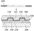
10:金凸块结构 11:凸块下金属层10: Gold bump structure 11: UBM layer
12:金凸块层 20:硅基板12: Gold bump layer 20: Silicon substrate
21:焊垫 22:保护层21: Welding pad 22: Protective layer
23:开口 100:凸块结构23: Opening 100: Bump structure
110:第一高分子块体 111:第一上表面110: first polymer block 111: first upper surface
112:第一接合槽 120:第二高分子块体112: The first joint groove 120: The second polymer block
121:第二上表面 122:第二接合槽121: Second upper surface 122: Second engagement groove
130:第一沟槽 140:凸块下金属层130: first groove 140: under bump metal layer
141:第二沟槽 142:第三接合槽141: Second Groove 142: Third Engagement Groove
143:第四接合槽 150:接合金属层143: Fourth joint slot 150: Joint metal layer
151:第三沟槽 152:第五接合槽151: The third groove 152: The fifth joint groove
153:第六接合槽 200:载板153: The sixth joint slot 200: Carrier board
210:焊垫 220:保护层210: welding pad 220: protective layer
221:开口 300:高分子层221: opening 300: polymer layer
310:高分子凸块 400:第一光罩310: polymer bump 400: first photomask
500:光刻胶 510:开口500: Photoresist 510: Opening
600:第二光罩 700:接点600: Second mask 700: Contact
710:下表面 W1:第一宽度710: lower surface W1: first width
W2:第二宽度 W3:第三宽度W2: second width W3: third width
具体实施方式Detailed ways
为更进一步阐述本发明为达成预定发明目的所采取的技术手段及功效,以下结合附图及较佳实施例,对依据本发明提出的凸块结构及制造工艺其具体实施方式、结构、制造方法、步骤、特征及其功效,详细说明如后。In order to further explain the technical means and effects of the present invention to achieve the intended purpose of the invention, the specific implementation, structure and manufacturing method of the bump structure and manufacturing process proposed according to the present invention will be described below in conjunction with the accompanying drawings and preferred embodiments. , steps, features and effects thereof are described in detail below.
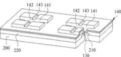
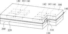
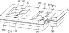
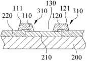
请参阅图2及图3,其本发明的一较佳实施例,一种凸块结构100其设置于一载板200上,该载板200具有多个焊垫210及一保护层220,该保护层220具有多个开口221,所述开口221显露出所述焊垫210,该凸块结构100与各该焊垫210电性连接,该凸块结构100包含有一第一高分子块体110、一第二高分子块体120、一第一沟槽130、一凸块下金属层140及一接合金属层150,其中该第一高分子块体110及第二高分子块体120分别为一独立的块体,该第一高分子决体110及该第二高分子块体120位于该第一沟槽130的二侧,且该第一沟槽130显露出该焊垫210,请参阅图3及图5E,该第一高分子块体110及第二高分子块体120设置于该焊垫210及该保护层220上,该第一高分子块体110具有一第一上表面111及一凹设于该第一上表面111的第一接合槽112,该第二高分子块体120具有一第二上表面121及一凹设于该第二上表面121的第二接合槽122,该第一高分子块体110的该第一接合槽112及该第二高分子块体120的该第二接合槽122连通该第一沟槽130,该凸块下金属层140(UBM)覆盖该焊垫210,该凸块下金属层140形成有一第二沟槽141、一第三接合槽142及一第四接合槽143,该第三接合槽142及该第四接合槽143连通该第二沟槽141,该凸块下金属层140的材质可为钛化钨/金(TiW/Au),该接合金属层150覆盖该凸块下金属层140,该接合金属层150的材质可为金(Au),该接合金属层150并形成有一第三沟槽151、一第五接合槽152及一第六接合槽153,该第五接合槽152及该第六接合槽153连通该第三沟槽151,在本实施例中,该第三沟槽151、该第五接合槽152及该第六接合槽153构成一“+”形凹槽,其中该凸块下金属层140的该第二沟槽141位于该第一沟槽130与该接合金属层150的该第三沟槽151之间,该凸块下金属层140的该第三接合槽142位于该第一高分子块体110的该第一接合槽112与该接合金属层150的该第五接合槽152之间,该凸块下金属层140的第四接合槽143位于该第二高分子块体120的该第二接合槽122与该接合金属层150的该第六接合槽153之间,该第三沟槽151具有一第一宽度W1,该第五接合槽152具有一第二宽度W2,该第六接合槽152具有一第三宽度W3,该第一宽度W1大于该第二宽度W2,且该第一宽度W1大于该第三宽度W3。Please refer to FIG. 2 and FIG. 3, a preferred embodiment of the present invention, a bump structure 100 is disposed on a carrier 200, the carrier 200 has a plurality of solder pads 210 and a protective layer 220, the The protection layer 220 has a plurality of openings 221, the openings 221 expose the pads 210, the bump structure 100 is electrically connected to each of the pads 210, and the bump structure 100 includes a first polymer block 110 , a second polymer block 120, a first groove 130, an UBM layer 140 and a bonding metal layer 150, wherein the first polymer block 110 and the second polymer block 120 are respectively An independent block, the first polymer block 110 and the second polymer block 120 are located on two sides of the first trench 130, and the first trench 130 exposes the pad 210, please refer to 3 and 5E, the first polymer block 110 and the second polymer block 120 are disposed on the pad 210 and the protective layer 220, and the first polymer block 110 has a first upper surface 111 and a first engaging groove 112 recessed on the first upper surface 111, the second polymer block 120 has a second upper surface 121 and a second engaging groove 122 recessed on the second upper surface 121 , the first bonding groove 112 of the first polymer block 110 and the second bonding groove 122 of the second polymer block 120 communicate with the first groove 130, the under bump metal layer 140 (UBM) Covering the pad 210, the UBM layer 140 forms a second groove 141, a third bonding groove 142 and a fourth bonding groove 143, the third bonding groove 142 and the fourth bonding groove 143 communicate with the The second groove 141, the material of the UBM layer 140 can be titanium tungsten/gold (TiW/Au), the bonding metal layer 150 covers the UBM layer 140, and the material of the bonding metal layer 150 can be It is gold (Au), and the bonding metal layer 150 is formed with a third groove 151, a fifth bonding groove 152 and a sixth bonding groove 153, and the fifth bonding groove 152 and the sixth bonding groove 153 communicate with the first bonding groove 153. Three
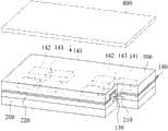
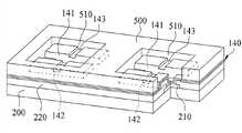
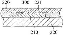
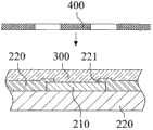
请参阅图4A至图4M及图5A至图5M,其为本发明该凸块结构100的制造工艺,包含下列步骤,首先,请参阅图4A及图5A,提供一载板200,其具有多个焊垫210及一保护层220,该保护层220具有多个开口221,所述开口221显露出所述焊垫210。之后,请参阅图4B及图5B,在该载板200上形成一高分子层300,该高分子层300覆盖该保护层220及所述焊垫210。接着,请参阅图4C及图5C,提供一第一光罩400并进行第一次曝光步骤。之后,请参阅图4D及图5D,移除该第一光罩400并进行第一次显影步骤,以使该高分子层300形成有多个高分子凸块310,且每一高分子凸块310对应一焊垫210,各该高分子凸块310包含有一第一高分子块体110、一第二高分子块体120及一第一沟槽130,该第一高分子块体110及该第二高分子块体120分别为一独立的块体,其分别位于该第一沟槽130的二侧,该第一沟槽130显露出该焊垫210,且该第一高分子块体110及该第二高分子块体120设置于该焊垫210及该保护层220上,请参阅图4,该第一高分子块体110具有一第一上表面111及一凹设于该第一上表面111的第一接合槽112,该第二高分子块体120具有一第二上表面121及一凹设于该第二上表面121的第二接合槽122,其中该第一高分子块体110的该第一接合槽112及该第二高分子块体120的该第二接合槽122连通该第一沟槽130。接着,请参阅图4E及图5E,固化所述高分子凸块310。之后,请参阅图4F及图5F,在该载板200上形成一凸块下金属层140(UBM),该凸块下金属层140覆盖该保护层220、该焊垫210、该第一高分子块体110及该第二高分子块体120,请参阅图4D及图4F,其中该凸块下金属层140形成有一第二沟槽141、一第三接合槽142及一第四接合槽143,该第三接合槽142及该第四接合槽143连通该第二沟槽141,该第二沟槽141位于该第一沟槽130上方,该第三接合槽142位于该第一接合槽112上方,该第四接合槽143位于该第二接合槽122上方。接着,请参阅图4G及图5G,在该凸块下金属层上形成一光刻胶500。之后,请参阅图4H及图5H,提供一第二光罩600并进行第二次曝光步骤。接着,请参阅图4I及图5I,移除该第二光罩600并进行第二次显影步骤,以使该光刻胶500形成有多个开口510,各该开口510对应各该高分子凸块310,且各该开口510并显露出位在各该开口510中的该凸块下金属层140。之后,请参阅图4J及图5J,在所述开口510中形成一接合金属层150,该接合金属层150覆盖被所述开口510显露的该凸块下金属层140,其中该接合金属层150形成有一第三沟槽151、一第五接合槽152及一第六接合槽153,该第五接合槽152及该第六接合槽153连通该第三沟槽151,请参阅图3,该第三沟槽151位于该第二沟槽141上方,该第五接合槽152位于该第三接合槽142上方,该第六接合槽153位于该第四接合槽143上方。接着,请参阅图4K及图5K,移除该光刻胶500,以显露未被该接合金属层150覆盖的该凸块下金属层140。最后,请参阅图4L、图5L及图3,移除未被该接合金属层150覆盖的该凸块下金属层140,以使该凸块下金属层140仅覆盖该第一高分子块体110及该第二高分子块体120。Please refer to FIG. 4A to FIG. 4M and FIG. 5A to FIG. 5M, which is the manufacturing process of the
请参阅图6,当本发明的该凸块结构100与另一电子元件的接点700(如连接垫或引脚)共晶接合(eutectic bonding)时,该接点700的一下表面710被触压结合于该凸块结构100的该接合金属层140,且该接点700的一部份嵌入该接合金属层150的该第三沟槽151、该第五接合槽152及该第六接合槽153中,其可增加该凸块结构100与该接点700的接触面积,并可提高该接点700与该凸块结构100的共晶可靠度,并且由于该接点700的一部份嵌入该接合金属层150该第五接合槽152及该第六接合槽153中,因此可避免该接点700发生偏移的情形,此外由于该凸块结构100以该第一高分子块体110及第二高分子块体120为衬底材料,因此可节省电镀材料成本。Please refer to FIG. 6 , when the
以上所述,仅是本发明的较佳实施例而已,并非对本发明作任何形式上的限制,虽然本发明已以较佳实施例揭露如上,然而并非用以限定本发明,任何熟悉本专业的技术人员,在不脱离本发明技术方案范围内,当可利用上述揭示的方法及技术内容作出些许的更动或修饰为等同变化的等效实施例,但凡是未脱离本发明技术方案的内容,依据本发明的技术实质对以上实施例所作的任何简单修改、等同变化与修饰,均仍属于本发明技术方案的范围内。The above description is only a preferred embodiment of the present invention, and does not limit the present invention in any form. Although the present invention has been disclosed as above with preferred embodiments, it is not intended to limit the present invention. Anyone familiar with this field Those skilled in the art, without departing from the scope of the technical solution of the present invention, may use the method and technical content disclosed above to make some changes or modifications to equivalent embodiments with equivalent changes, but if they do not depart from the technical solution of the present invention, Any simple modifications, equivalent changes and modifications made to the above embodiments according to the technical essence of the present invention still fall within the scope of the technical solution of the present invention.
Claims (8)
Priority Applications (1)
| Application Number | Priority Date | Filing Date | Title |
|---|---|---|---|
| CN201110134729.4ACN102790016B (en) | 2011-05-16 | 2011-05-16 | Bump structure and manufacturing process |
Applications Claiming Priority (1)
| Application Number | Priority Date | Filing Date | Title |
|---|---|---|---|
| CN201110134729.4ACN102790016B (en) | 2011-05-16 | 2011-05-16 | Bump structure and manufacturing process |
Publications (2)
| Publication Number | Publication Date |
|---|---|
| CN102790016Atrue CN102790016A (en) | 2012-11-21 |
| CN102790016B CN102790016B (en) | 2014-10-15 |
Family
ID=47155386
Family Applications (1)
| Application Number | Title | Priority Date | Filing Date |
|---|---|---|---|
| CN201110134729.4AActiveCN102790016B (en) | 2011-05-16 | 2011-05-16 | Bump structure and manufacturing process |
Country Status (1)
| Country | Link |
|---|---|
| CN (1) | CN102790016B (en) |
Cited By (2)
| Publication number | Priority date | Publication date | Assignee | Title |
|---|---|---|---|---|
| CN109786349A (en)* | 2018-01-11 | 2019-05-21 | 苏州能讯高能半导体有限公司 | A kind of exhaust device and device welding structure |
| WO2022007267A1 (en)* | 2020-07-09 | 2022-01-13 | 江苏纳沛斯半导体有限公司 | Semiconductor encapsulation structure and manufacturing method therefor |
Citations (5)
| Publication number | Priority date | Publication date | Assignee | Title |
|---|---|---|---|---|
| JP2001085560A (en)* | 1999-09-13 | 2001-03-30 | Sharp Corp | Semiconductor device and method of manufacturing the same |
| US20020180064A1 (en)* | 2001-06-05 | 2002-12-05 | Chipbond Technology Corporation | Metallized surface wafer level package structure |
| CN1585122A (en)* | 2004-06-04 | 2005-02-23 | 友达光电股份有限公司 | Composite bump structure and manufacturing method |
| CN101266936A (en)* | 2008-04-30 | 2008-09-17 | 日月光半导体制造股份有限公司 | Bump manufacturing process |
| CN101567348A (en)* | 2008-04-21 | 2009-10-28 | 南茂科技股份有限公司 | Chip structure with bump and forming method |
- 2011
- 2011-05-16CNCN201110134729.4Apatent/CN102790016B/enactiveActive
Patent Citations (5)
| Publication number | Priority date | Publication date | Assignee | Title |
|---|---|---|---|---|
| JP2001085560A (en)* | 1999-09-13 | 2001-03-30 | Sharp Corp | Semiconductor device and method of manufacturing the same |
| US20020180064A1 (en)* | 2001-06-05 | 2002-12-05 | Chipbond Technology Corporation | Metallized surface wafer level package structure |
| CN1585122A (en)* | 2004-06-04 | 2005-02-23 | 友达光电股份有限公司 | Composite bump structure and manufacturing method |
| CN101567348A (en)* | 2008-04-21 | 2009-10-28 | 南茂科技股份有限公司 | Chip structure with bump and forming method |
| CN101266936A (en)* | 2008-04-30 | 2008-09-17 | 日月光半导体制造股份有限公司 | Bump manufacturing process |
Cited By (2)
| Publication number | Priority date | Publication date | Assignee | Title |
|---|---|---|---|---|
| CN109786349A (en)* | 2018-01-11 | 2019-05-21 | 苏州能讯高能半导体有限公司 | A kind of exhaust device and device welding structure |
| WO2022007267A1 (en)* | 2020-07-09 | 2022-01-13 | 江苏纳沛斯半导体有限公司 | Semiconductor encapsulation structure and manufacturing method therefor |
Also Published As
| Publication number | Publication date |
|---|---|
| CN102790016B (en) | 2014-10-15 |
Similar Documents
| Publication | Publication Date | Title |
|---|---|---|
| US8119451B2 (en) | Method of manufacturing semiconductor package and method of manufacturing substrate for the semiconductor package | |
| TWI611521B (en) | Semiconductor package and semiconductor device | |
| CN101083238A (en) | Microelectronic element with elastic conductive projection and method of manufacture | |
| TWI434383B (en) | Bonding pad structure and integrated cicruit comprise a pluirality of bonding pad structures | |
| JP5290215B2 (en) | Semiconductor device, semiconductor package, interposer, and manufacturing method of interposer | |
| JP4729963B2 (en) | PROJECT ELECTRODE FOR CONNECTING ELECTRONIC COMPONENT, ELECTRONIC COMPONENT MOUNTING BODY USING SAME, AND METHOD FOR PRODUCING THEM | |
| TW200812037A (en) | Circuit substrate and semiconductor device | |
| CN202394889U (en) | Semiconductor packaging structure | |
| JP4887997B2 (en) | Electronic component mounting method | |
| JP5569676B2 (en) | Electronic component mounting method | |
| KR102006637B1 (en) | Method Of Forming Bump And Semiconductor device including The Same | |
| CN101404268A (en) | Semiconductor element and bump manufacturing method | |
| CN102790016B (en) | Bump structure and manufacturing process | |
| CN102790035B (en) | Bump structure and process | |
| KR100635425B1 (en) | Structure and method for bonding an ic chip | |
| TWI423353B (en) | Bump structure and process of manufacturing the same | |
| TWI406378B (en) | Bump structure and process of manufacturing the same | |
| CN101989590B (en) | bump structure | |
| JP4118974B2 (en) | IC chip mounting substrate and method of manufacturing IC chip mounting substrate | |
| TWI606466B (en) | Nuclear layer technology anisotropic conductive film | |
| TWM412460U (en) | Bump structure | |
| TWM412576U (en) | Bump structure | |
| US8330280B1 (en) | Bump structure and process of manufacturing the same | |
| JP5067247B2 (en) | Electronic equipment | |
| KR20110015904A (en) | Solder bump manufacturing method |
Legal Events
| Date | Code | Title | Description |
|---|---|---|---|
| C06 | Publication | ||
| PB01 | Publication | ||
| C10 | Entry into substantive examination | ||
| SE01 | Entry into force of request for substantive examination | ||
| C14 | Grant of patent or utility model | ||
| GR01 | Patent grant |