CN102779756A - Method for manufacturing semiconductor power device - Google Patents
Method for manufacturing semiconductor power deviceDownload PDFInfo
- Publication number
- CN102779756A CN102779756ACN201110170133XACN201110170133ACN102779756ACN 102779756 ACN102779756 ACN 102779756ACN 201110170133X ACN201110170133X ACN 201110170133XACN 201110170133 ACN201110170133 ACN 201110170133ACN 102779756 ACN102779756 ACN 102779756A
- Authority
- CN
- China
- Prior art keywords
- layer
- semiconductor
- manufacture method
- power devices
- semiconductor power
- Prior art date
- Legal status (The legal status is an assumption and is not a legal conclusion. Google has not performed a legal analysis and makes no representation as to the accuracy of the status listed.)
- Granted
Links
- 238000000034methodMethods0.000titleclaimsabstractdescription59
- 239000004065semiconductorSubstances0.000titleclaimsabstractdescription57
- 238000004519manufacturing processMethods0.000titleclaimsabstractdescription21
- 239000002019doping agentSubstances0.000claimsabstractdescription31
- 239000000758substrateSubstances0.000claimsabstractdescription15
- 230000003647oxidationEffects0.000claimsabstractdescription11
- 238000007254oxidation reactionMethods0.000claimsabstractdescription11
- 238000005516engineering processMethods0.000claimsdescription4
- VYPSYNLAJGMNEJ-UHFFFAOYSA-NSilicium dioxideChemical compoundO=[Si]=OVYPSYNLAJGMNEJ-UHFFFAOYSA-N0.000claimsdescription3
- 229910021420polycrystalline siliconInorganic materials0.000claimsdescription3
- 229910052710siliconInorganic materials0.000claimsdescription3
- 239000010703siliconSubstances0.000claimsdescription3
- OAICVXFJPJFONN-UHFFFAOYSA-NPhosphorusChemical compound[P]OAICVXFJPJFONN-UHFFFAOYSA-N0.000claimsdescription2
- 229910052581Si3N4Inorganic materials0.000claimsdescription2
- 229910021417amorphous siliconInorganic materials0.000claimsdescription2
- 229910052698phosphorusInorganic materials0.000claimsdescription2
- 239000011574phosphorusSubstances0.000claimsdescription2
- HQVNEWCFYHHQES-UHFFFAOYSA-Nsilicon nitrideChemical compoundN12[Si]34N5[Si]62N3[Si]51N64HQVNEWCFYHHQES-UHFFFAOYSA-N0.000claimsdescription2
- 230000002262irrigationEffects0.000claims2
- 238000003973irrigationMethods0.000claims2
- 238000009792diffusion processMethods0.000claims1
- 238000002347injectionMethods0.000claims1
- 239000007924injectionSubstances0.000claims1
- 229920005591polysiliconPolymers0.000claims1
- 239000000377silicon dioxideSubstances0.000claims1
- 238000007517polishing processMethods0.000abstractdescription12
- 239000010410layerSubstances0.000description119
- 230000002093peripheral effectEffects0.000description14
- 229920002120photoresistant polymerPolymers0.000description12
- 230000007704transitionEffects0.000description10
- 238000005530etchingMethods0.000description8
- 150000002500ionsChemical class0.000description6
- 239000004020conductorSubstances0.000description5
- 238000005468ion implantationMethods0.000description5
- 229910052751metalInorganic materials0.000description5
- 239000002184metalSubstances0.000description5
- 238000000206photolithographyMethods0.000description5
- 238000005498polishingMethods0.000description5
- 230000005540biological transmissionEffects0.000description4
- 239000000203mixtureSubstances0.000description4
- 239000011159matrix materialSubstances0.000description3
- 239000000126substanceSubstances0.000description3
- XUIMIQQOPSSXEZ-UHFFFAOYSA-NSiliconChemical compound[Si]XUIMIQQOPSSXEZ-UHFFFAOYSA-N0.000description2
- 239000005380borophosphosilicate glassSubstances0.000description2
- 238000010586diagramMethods0.000description2
- 230000005669field effectEffects0.000description2
- 239000007769metal materialSubstances0.000description2
- 229910004298SiO 2Inorganic materials0.000description1
- RTAQQCXQSZGOHL-UHFFFAOYSA-NTitaniumChemical compound[Ti]RTAQQCXQSZGOHL-UHFFFAOYSA-N0.000description1
- 239000002253acidSubstances0.000description1
- 239000012790adhesive layerSubstances0.000description1
- 229910052782aluminiumInorganic materials0.000description1
- XAGFODPZIPBFFR-UHFFFAOYSA-NaluminiumChemical compound[Al]XAGFODPZIPBFFR-UHFFFAOYSA-N0.000description1
- 230000004888barrier functionEffects0.000description1
- 238000003486chemical etchingMethods0.000description1
- 238000006243chemical reactionMethods0.000description1
- 238000005229chemical vapour depositionMethods0.000description1
- 239000011248coating agentSubstances0.000description1
- 238000000576coating methodMethods0.000description1
- 238000001312dry etchingMethods0.000description1
- 230000005684electric fieldEffects0.000description1
- 238000009413insulationMethods0.000description1
- 239000000463materialSubstances0.000description1
- 229910044991metal oxideInorganic materials0.000description1
- 150000004706metal oxidesChemical class0.000description1
- 238000012986modificationMethods0.000description1
- 230000004048modificationEffects0.000description1
- 239000011241protective layerSubstances0.000description1
- 229910052814silicon oxideInorganic materials0.000description1
- 239000010936titaniumSubstances0.000description1
- 229910052719titaniumInorganic materials0.000description1
Images


Classifications
- H—ELECTRICITY
- H10—SEMICONDUCTOR DEVICES; ELECTRIC SOLID-STATE DEVICES NOT OTHERWISE PROVIDED FOR
- H10D—INORGANIC ELECTRIC SEMICONDUCTOR DEVICES
- H10D30/00—Field-effect transistors [FET]
- H10D30/01—Manufacture or treatment
- H10D30/021—Manufacture or treatment of FETs having insulated gates [IGFET]
- H10D30/028—Manufacture or treatment of FETs having insulated gates [IGFET] of double-diffused metal oxide semiconductor [DMOS] FETs
- H10D30/0291—Manufacture or treatment of FETs having insulated gates [IGFET] of double-diffused metal oxide semiconductor [DMOS] FETs of vertical DMOS [VDMOS] FETs
- H—ELECTRICITY
- H10—SEMICONDUCTOR DEVICES; ELECTRIC SOLID-STATE DEVICES NOT OTHERWISE PROVIDED FOR
- H10D—INORGANIC ELECTRIC SEMICONDUCTOR DEVICES
- H10D30/00—Field-effect transistors [FET]
- H10D30/60—Insulated-gate field-effect transistors [IGFET]
- H10D30/64—Double-diffused metal-oxide semiconductor [DMOS] FETs
- H10D30/66—Vertical DMOS [VDMOS] FETs
- H10D30/665—Vertical DMOS [VDMOS] FETs having edge termination structures
- H—ELECTRICITY
- H01—ELECTRIC ELEMENTS
- H01L—SEMICONDUCTOR DEVICES NOT COVERED BY CLASS H10
- H01L21/00—Processes or apparatus adapted for the manufacture or treatment of semiconductor or solid state devices or of parts thereof
- H01L21/02—Manufacture or treatment of semiconductor devices or of parts thereof
- H01L21/04—Manufacture or treatment of semiconductor devices or of parts thereof the devices having potential barriers, e.g. a PN junction, depletion layer or carrier concentration layer
- H01L21/18—Manufacture or treatment of semiconductor devices or of parts thereof the devices having potential barriers, e.g. a PN junction, depletion layer or carrier concentration layer the devices having semiconductor bodies comprising elements of Group IV of the Periodic Table or AIIIBV compounds with or without impurities, e.g. doping materials
- H01L21/22—Diffusion of impurity materials, e.g. doping materials, electrode materials, into or out of a semiconductor body, or between semiconductor regions; Interactions between two or more impurities; Redistribution of impurities
- H01L21/225—Diffusion of impurity materials, e.g. doping materials, electrode materials, into or out of a semiconductor body, or between semiconductor regions; Interactions between two or more impurities; Redistribution of impurities using diffusion into or out of a solid from or into a solid phase, e.g. a doped oxide layer
- H01L21/2251—Diffusion into or out of group IV semiconductors
- H01L21/2254—Diffusion into or out of group IV semiconductors from or through or into an applied layer, e.g. photoresist, nitrides
- H01L21/2257—Diffusion into or out of group IV semiconductors from or through or into an applied layer, e.g. photoresist, nitrides the applied layer being silicon or silicide or SIPOS, e.g. polysilicon, porous silicon
- H—ELECTRICITY
- H10—SEMICONDUCTOR DEVICES; ELECTRIC SOLID-STATE DEVICES NOT OTHERWISE PROVIDED FOR
- H10D—INORGANIC ELECTRIC SEMICONDUCTOR DEVICES
- H10D62/00—Semiconductor bodies, or regions thereof, of devices having potential barriers
- H10D62/10—Shapes, relative sizes or dispositions of the regions of the semiconductor bodies; Shapes of the semiconductor bodies
- H10D62/17—Semiconductor regions connected to electrodes not carrying current to be rectified, amplified or switched, e.g. channel regions
- H10D62/393—Body regions of DMOS transistors or IGBTs
Landscapes
- Electrodes Of Semiconductors (AREA)
Abstract
Translated fromChinese
Description
Translated fromChinese技术领域technical field
本发明涉及一种半导体功率装置的制作方法,特别是涉及一种可消除微刮痕的半导体功率装置的制作方法。The invention relates to a manufacturing method of a semiconductor power device, in particular to a manufacturing method of a semiconductor power device capable of eliminating micro scratches.
背景技术Background technique
功率半导体装置常常被应用在电源管理的领域,例如,切换式电源供应器、计算机中心或周边电源管理IC、背光板电源供应器或马达控制等等用途,其种类包括有绝缘栅双极性晶体管(insulated gate bipolar transistor,IGBT)、金氧半场效晶体管(metal-oxide-semiconductor field effect transistor,MOSFET)与双载子接面晶体管(bipolar junction transistor,BJT)等装置。其中,由于金氧半场效晶体管可以节省电能而且可以提供比较快的装置切换速度,所以被广泛地应用各领域中。Power semiconductor devices are often used in the field of power management, such as switching power supply, computer center or peripheral power management IC, backlight power supply or motor control, etc., and its types include insulated gate bipolar transistors (insulated gate bipolar transistor, IGBT), metal-oxide-semiconductor field effect transistor (MOSFET) and bipolar junction transistor (bipolar junction transistor, BJT) and other devices. Among them, metal oxide semiconductor field effect transistors are widely used in various fields because they can save power and provide relatively fast device switching speeds.
在功率装置中,基底是P型外延层与N型外延层交替设置,所以在衬底中会有许多个垂直于衬底表面的PN接面,而且这些PN接面互相平行,所以又被叫做超级接面结构。现有技术制作超级接面结构的技术,包括先在一第一导电型基底(例如:N型基底)上成长一第一导电型外延层(例如:N型外延层)和一硬掩模,然后利用一第一掩模,在第一导电型外延层及硬掩模蚀刻出多个沟渠。接着,在各个沟渠内形成一第二导电型外延层(例如:P型外延层),并进行抛光工艺和回蚀刻工艺,使第二导电型外延层的上表面与第一导电型外延层的上表面切齐。到现在,各个沟渠内已经填满了第二导电型外延层并且被第一导电型外延层包围。而多个第二导电型外延层和第一导电型外延层的接触面会形成超级接面结构。In a power device, the substrate is alternately arranged with P-type epitaxial layers and N-type epitaxial layers, so there will be many PN junctions perpendicular to the substrate surface in the substrate, and these PN junctions are parallel to each other, so they are also called super junction structure. The prior art technology for making a super junction structure includes first growing a first conductivity type epitaxial layer (for example: N type epitaxial layer) and a hard mask on a first conductivity type substrate (for example: N type substrate), Then using a first mask, a plurality of trenches are etched in the epitaxial layer of the first conductivity type and the hard mask. Next, a second conductivity type epitaxial layer (for example: P-type epitaxial layer) is formed in each trench, and a polishing process and an etch-back process are performed to make the upper surface of the second conductivity type epitaxial layer and the first conductivity type epitaxial layer Cut the top surface evenly. Up to now, each trench has been filled with the second conductivity type epitaxial layer and surrounded by the first conductivity type epitaxial layer. The contact surfaces of the plurality of epitaxial layers of the second conductivity type and the epitaxial layers of the first conductivity type will form a super junction structure.
但是,上述的现有技术仍有问题需要被解决。举例来说,上述技术是藉由一抛光工艺,使第二导电型外延层的上表面与硬掩模的表面对齐。因为抛光包括有物理作用力,所以一定会对第二导电型外延层的上表面产生微刮痕(micro scratch),而所述的微刮痕会影响金属导体和外延层接面间的电流传输,所以降低了功率装置的电性表现和工艺良率。可知,仍然需要一种超级接面的功率半导体装置的制作方法,用来制作具有较少微刮痕的功率半导体装置,提升功率半导体装置的良率,这是业界想要努力达到的目标。However, the above-mentioned prior art still has problems to be solved. For example, the above technology uses a polishing process to align the top surface of the second conductivity type epitaxial layer with the surface of the hard mask. Because polishing includes physical force, it will definitely produce micro scratches (micro scratches) on the upper surface of the second conductivity type epitaxial layer, and the micro scratches will affect the current transmission between the metal conductor and the epitaxial layer junction. , so the electrical performance and process yield of the power device are reduced. It can be seen that there is still a need for a method for manufacturing a super-junction power semiconductor device, which is used to manufacture a power semiconductor device with less micro-scratch and improve the yield of the power semiconductor device. This is the goal that the industry wants to strive to achieve.
发明内容Contents of the invention
本发明的主要目的在于提供一种功率半导体装置的制作方法,能够提升功率半导体装置的电性及良率。The main purpose of the present invention is to provide a method for manufacturing a power semiconductor device, which can improve the electrical performance and yield of the power semiconductor device.
本发明提供一种半导体功率装置的制作方法。首先,提供一衬底,其上包括有至少一半导体层和一衬垫层。接着,在衬垫层及半导体层内蚀刻出至少一沟渠,并在沟渠内及衬垫层上形成一掺质来源层。进行一热驱入工艺,将掺质来源层的掺质扩散到半导体层,并进行一抛光工艺,去除衬垫层上的掺质来源层。接着,进行一热氧化工艺,用来消除抛光工艺造成的微刮痕。最后,去除衬垫层,用来暴露出半导体层。The invention provides a method for manufacturing a semiconductor power device. First, a substrate is provided, including at least one semiconductor layer and a liner layer thereon. Next, at least one trench is etched in the liner layer and the semiconductor layer, and a dopant source layer is formed in the trench and on the liner layer. A thermal driving process is performed to diffuse the dopants in the dopant source layer to the semiconductor layer, and a polishing process is performed to remove the dopant source layer on the liner layer. Next, a thermal oxidation process is performed to eliminate micro-scratches caused by the polishing process. Finally, the pad layer is removed to expose the semiconductor layer.
本发明提供一热氧化工艺(thermal oxidation process),用来消除因为抛光工艺而产生在掺质来源层表面的微刮痕,可以帮助金属导体和掺质来源层接面间的电流传输,并且提升功率半导体装置的良率。The present invention provides a thermal oxidation process (thermal oxidation process), which is used to eliminate micro-scratches on the surface of the dopant source layer due to the polishing process, which can help the current transmission between the metal conductor and the dopant source layer junction, and improve Yield of power semiconductor devices.
附图说明Description of drawings
图1到图11是一种半导体功率装置的制作方法示意图。1 to 11 are schematic diagrams of a manufacturing method of a semiconductor power device.
其中,附图标记说明如下:Wherein, the reference signs are explained as follows:
12 第一导电型基底 14 晶胞区12 Substrate of the
16 外围耐压区 15 过渡区16 Peripheral
18 半导体层 20 衬垫层18
20a 上层衬垫层 20b 下层衬垫层20a
24、26 沟渠 30 掺质来源层24, 26 Ditch 30 Dopant source layer
34 基体掺质区 32 氧化层34 Matrix
48 栅极氧化层 40 场氧化层48
50 栅极导电层 50a 栅极图案50 Gate
50b 栅极图案 51 光致抗蚀剂图案
52 离子井 53 光致抗蚀剂图案52 Ion Well 53 Photoresist Pattern
53a 开口 54 源极掺杂区
56 衬垫层 58 绝缘层56
60 接触洞开口 62 接触洞开口60 Contact Hole Opening 62 Contact Hole Opening
66 掺杂区 68 接触插塞66 Doped region 68 Contact plug
74a 栅极导线 74b 源极电极74a Gate Wire 74b Source Electrode
76 保护层76 protective layer
具体实施方式Detailed ways
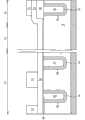
图1到图10是制作一种功率装置的方法示意图,其中的功率装置可以包括沟渠式的功率晶体管,而附图中相同的装置或部位是使用相同的标记。需要注意的是,附图是用来说明是目的,并没有按照原尺寸作图。1 to 10 are schematic diagrams of a method of manufacturing a power device, wherein the power device may include a trench-type power transistor, and the same devices or parts in the drawings use the same symbols. It should be noted that the drawings are for illustration purposes and are not drawn to original scale.
请参考图1,首先提供一第一导电型基底12,第一导电型基底12可以是N型掺杂硅基底,可以当作功率晶体管的一漏極。第一导电型基底12上定义有一晶胞区(cell region)14、一围绕晶胞区14的外围耐压区(terminationregion)16、和一设置在晶胞区14和外围耐压区16间的过渡区(transitionregion)15,其中晶胞区14用于设置具有开关功能的晶体管装置,而外围耐压区16包括用来阻挡晶胞区14的高强度电场向外扩散的耐压结构。接着,可以利用外延工艺于第一导电型基底12上形成一第一导电型半导体层18。根据本发明的优选实施例,半导体层18可以是一N型外延层,例如,可以利用一化学气相沉积工艺或其它适合的方法形成,而半导体层18同时可作是所想要形成的功率装置的飘移层(drift layer)。接着,于半导体层18上形成一衬垫层20,此衬垫层20可以包括上、下两部分,上层衬垫层20a的组成可以是氮化硅(Si3N4),而下层衬垫层20b的组成可以是硅氧层(SiO2)。Referring to FIG. 1 , firstly, a substrate 12 of a first conductivity type is provided. The substrate 12 of the first conductivity type can be an N-type doped silicon substrate, and can be used as a drain of a power transistor. A cell region (cell region) 14, a peripheral withstand voltage region (terminationregion) 16 surrounding the
接着,利用光刻和蚀刻工艺,于衬垫层20和半导体层18中形成至少一沟渠24、26,其中,沟渠24位于晶胞区域14内,而沟渠26位于外围耐压区16内。沟渠24、26的形成方式,举例来说,可以先在衬垫层20上涂上一光致抗蚀剂层(图未示),接着利用具有沟渠图案的光掩模当作曝光掩模,对光致抗蚀剂层(图未示)进行一光刻工艺,再利用图案化的光致抗蚀剂层当作蚀刻掩模,对衬垫层20进行一各向異性蚀刻工艺,将光罩上的沟渠图案转移到衬垫层20,接下来,去除图案化的光致抗蚀剂层,再进行干蚀刻工艺,将沟渠图案转移到半导体层18中。当然,上述形成沟渠的方法只是范例,沟渠24、26也可以利用其它方法形成。本发明沟渠的形状、位置、深度、宽度、长度与数量等特征不用受到图1的沟渠24、26所局限,而且可以根据实际的产品设计需求或工艺特性而调整,例如沟渠24、26的布局可以是具有条状(strip)、六边形(hexagonal)或螺旋状(spiral)等图案。Next, at least one
请参考图2,接着,形成一掺质来源层30于沟渠24、26内和衬垫层20上,其中掺质来源层30具有一第二导电型,例如P型,而且掺质来源层30的材料包括外延硅、多晶硅或非晶硅,但不限于此。然后,进行一热驱入工艺,将掺质来源层30的掺质扩散到半导体层18中,所述的掺质可包括有磷。到目前为止,沟渠24、26周围和底部的半导体层18内已经形成具有一第二导电型基体掺质区34,其中第二导电型基体掺质区34与半导体层18间具有垂直PN接面,也就是超级接面。Please refer to FIG. 2, then, form a
然后,参考图3,进行一抛光工艺,去除衬垫层20上的掺质来源层30,直到暴露出衬垫层20的上表面,其中,抛光工艺是一化学机械抛光工艺(chemical mechanical polishing,CMP)。在现有技术中,因为化学机械抛光同时包括化学蚀刻反应用和物理抛光作用,此物理抛光作用一定会对掺质来源层30的上表面产生微刮痕(micro scratch),而且所述的微刮痕会影响金属导体和掺质来源层30间的电流传输,降低功率装置的电性表现和工艺良率。因此,根据本发明的优选实施例,提供一热氧化工艺(thermal oxidation process),用来消除抛光工艺所造成的掺质来源层30表面的微刮痕。接着,进行一热氧化工艺,形成一氧化层32位于掺质来源层30的上半部,其中,所述的热氧化工艺温度在800℃到1200℃间。Then, with reference to FIG. 3, a polishing process is performed to remove the
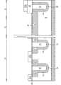
接着,参考图4,进行一蚀刻工艺,此蚀刻可以是一酸液蚀刻,用来同时去除半导体层18上方的衬垫层20(图未示)和沟渠24、26内部的氧化层32(图未示),暴露出半导体层18的上表面。这个时候,沟渠24、26内的掺质来源层30的上表面大概与半导体层18的上表面对齐。Next, with reference to FIG. 4 , an etching process is performed, which can be an acid etching, to simultaneously remove the pad layer 20 (not shown) above the
参考图5,于晶胞区14和过渡区15内的半导体层18的上表面形成一栅极氧化层48,接着于外围耐压区16的沟渠26上方形成一场氧化层40,其中场氧化层40的组成可包括氧硅化物。Referring to FIG. 5, a
参考图6,接着,全面沈积一栅极导电层50。根据本发明的优选实施例,栅极导电层50可以包括掺杂多晶硅(doped poly-silicon)。并且进行一光刻工艺,形成一光致抗蚀剂图案51,其包括多个开口(图未示),暴露出一部分的栅极导电层50。光致抗蚀剂图案51的用途是用来转移其图形到栅极导电层50。Referring to FIG. 6 , next, a gate
参考图7,进行一蚀刻工艺,经由开口51a(图未示)蚀刻部分的栅极导电层50(图未示),形成栅极图案50a、50b,其中栅极图案50b位于外围耐压区16内的场氧化层40上方。然后,去除光致抗蚀剂图案51(图未示)。接下来,进行一自我对准离子注入工艺,于沟渠24、26旁的导体层18中形成一第二导电型离子井52,例如,P型井。接下来,可以继续进行一热驱入工艺,用来活化第二导电型离子井52内的掺质。Referring to FIG. 7, an etching process is performed to etch part of the gate conductive layer 50 (not shown) through the opening 51a (not shown) to form
参考图8,进行一光刻工艺,形成一光致抗蚀剂图案53,其包括一开口53a,暴露出晶胞区14。再进行另一离子注入工艺,于晶胞区14内的第二导电型离子井52内形成一第一导电型源极掺杂区54。于此离子注入工艺中,因为过渡区15和外围耐压区16受到光致抗蚀剂图案53保护,所以不会产生掺杂区。然后,去除光致抗蚀剂图案53。接下来,可继续进行一热驱入工艺。Referring to FIG. 8 , a photolithography process is performed to form a
参考图9,于晶胞区14、过渡区15和外围耐压区16的上表面全面沈积一衬垫层56和一绝缘层58。根据本发明的优选实施例,绝缘层58的组成可以包括硼磷硅玻璃(BPSG)。然后,可以继续进行一回流(reflow)工艺和/或回蚀刻工艺,使绝缘层58表面平坦化。Referring to FIG. 9 , a
参考图10,蚀刻晶胞区14、过渡区15和外围耐压区16内的部分绝缘层58和衬垫层56,使晶胞区14内的各个沟渠24上方形成一接触洞开口60,暴露出沟渠24内的掺质来源层30表面及一部分的第一导电型源极掺杂区54。同时,于过渡区15和外围耐压区16分别形成至少一接触洞开口62,用来暴露出部分离子井52和部分栅极图案50b的表面。接下来,进行一离子注入工艺,在晶胞区14内的掺质来源层30表面形成一第二导电型掺杂区66并同时于过渡区15内的离子井52表面形成一第二导电型掺杂区66。经由所述的离子注入工艺,可以增加半导体层18于后续工艺中和金属的导电性。Referring to FIG. 10 , etching part of the insulating
参考图11,然后,全面形成一导电层(图未示),导电层可以包括金属材料,例如钛、铝等,所述的导电层覆盖于绝缘层58上方并且填入接触洞开口60、62内,并且在填入金属材料前,可以于接触洞开口60、62中先形成黏合层或/与阻挡层。接着,再利用另一道光刻和蚀刻工艺去除外围耐压区16内的部分的导电层(图未示),用来形成至少一栅极导线74a与至少一源极电极74b。其中,栅极导线74a直接接触栅极图案50b的表面,而且源极电极74b直接接触并覆盖于晶胞区域14和过渡区15的绝缘层58和部分半导体层18上。接下来,于过渡区15和外围耐压区16内形成一层保护层76,保护层76覆盖住栅极导线74a,但暴露出源极电极74b,用来形成本发明的功率装置。Referring to FIG. 11 , then, a conductive layer (not shown) is formed on the entire surface. The conductive layer may include metal materials, such as titanium, aluminum, etc., and the conductive layer covers the insulating
本发明提供一热氧化工艺(thermal oxidation process),用来消除抛光工艺所造成的掺质来源层表面的微刮痕,帮助金属导体和掺质来源层接面间的电流传输,进一步地提升功率半导体装置的良率。The present invention provides a thermal oxidation process (thermal oxidation process), which is used to eliminate micro-scratches on the surface of the dopant source layer caused by the polishing process, helps the current transmission between the metal conductor and the dopant source layer junction, and further improves the power The yield rate of semiconductor devices.
以上所述仅为本发明的优选实施例,凡依本发明权利要求所做的均等变化与修饰,皆应属本发明的涵盖范围。The above descriptions are only preferred embodiments of the present invention, and all equivalent changes and modifications made according to the claims of the present invention shall fall within the scope of the present invention.
Claims (11)
Applications Claiming Priority (2)
| Application Number | Priority Date | Filing Date | Title |
|---|---|---|---|
| TW100116806 | 2011-05-13 | ||
| TW100116806ATWI441261B (en) | 2011-05-13 | 2011-05-13 | Semiconductor power device manufacturing method |
Publications (2)
| Publication Number | Publication Date |
|---|---|
| CN102779756Atrue CN102779756A (en) | 2012-11-14 |
| CN102779756B CN102779756B (en) | 2014-12-31 |
Family
ID=47124625
Family Applications (1)
| Application Number | Title | Priority Date | Filing Date |
|---|---|---|---|
| CN201110170133.XAExpired - Fee RelatedCN102779756B (en) | 2011-05-13 | 2011-06-21 | Method for manufacturing semiconductor power device |
Country Status (3)
| Country | Link |
|---|---|
| US (1) | US8536004B2 (en) |
| CN (1) | CN102779756B (en) |
| TW (1) | TWI441261B (en) |
Families Citing this family (8)
| Publication number | Priority date | Publication date | Assignee | Title |
|---|---|---|---|---|
| US8748973B2 (en)* | 2011-05-19 | 2014-06-10 | Anpec Electronics Corporation | Super junction transistor and fabrication method thereof |
| TW201334036A (en)* | 2012-02-02 | 2013-08-16 | Anpec Electronics Corp | Method for reducing surface doping concentration of diffusion doped region, manufacturing method of super interface structure, and manufacturing method of power transistor element |
| US9614043B2 (en) | 2012-02-09 | 2017-04-04 | Vishay-Siliconix | MOSFET termination trench |
| US9842911B2 (en) | 2012-05-30 | 2017-12-12 | Vishay-Siliconix | Adaptive charge balanced edge termination |
| CN105409006B (en)* | 2013-07-16 | 2019-02-19 | 松下知识产权经营株式会社 | semiconductor device |
| US9887259B2 (en) | 2014-06-23 | 2018-02-06 | Vishay-Siliconix | Modulated super junction power MOSFET devices |
| US9882044B2 (en) | 2014-08-19 | 2018-01-30 | Vishay-Siliconix | Edge termination for super-junction MOSFETs |
| US20170373142A1 (en)* | 2016-06-23 | 2017-12-28 | Littelfuse, Inc. | Semiconductor device having side-diffused trench plug |
Citations (4)
| Publication number | Priority date | Publication date | Assignee | Title |
|---|---|---|---|---|
| CN1790735A (en)* | 2004-11-08 | 2006-06-21 | 株式会社电装 | Silicon carbide semiconductor device and method for manufacturing the same |
| WO2008084519A1 (en)* | 2007-01-11 | 2008-07-17 | Shin-Etsu Handotai Co., Ltd. | Method for manufacturing silicon epitaxial wafer |
| CN101814436A (en)* | 2009-11-05 | 2010-08-25 | 苏州博创集成电路设计有限公司 | Method for preparing longitudinal high-pressure deep-slot transistor |
| CN101877307A (en)* | 2009-04-29 | 2010-11-03 | 上海华虹Nec电子有限公司 | Method for obtaining alternative P-type and N-type semiconductor device structure and device structure thereof |
Family Cites Families (13)
| Publication number | Priority date | Publication date | Assignee | Title |
|---|---|---|---|---|
| US4672407A (en)* | 1984-05-30 | 1987-06-09 | Kabushiki Kaisha Toshiba | Conductivity modulated MOSFET |
| US5273917A (en)* | 1989-08-19 | 1993-12-28 | Fuji Electric Co., Ltd. | Method for manufacturing a conductivity modulation MOSFET |
| JP4860022B2 (en)* | 2000-01-25 | 2012-01-25 | エルピーダメモリ株式会社 | Manufacturing method of semiconductor integrated circuit device |
| US8314002B2 (en)* | 2000-05-05 | 2012-11-20 | International Rectifier Corporation | Semiconductor device having increased switching speed |
| US6660571B2 (en)* | 2000-06-02 | 2003-12-09 | General Semiconductor, Inc. | High voltage power MOSFET having low on-resistance |
| US6479352B2 (en)* | 2000-06-02 | 2002-11-12 | General Semiconductor, Inc. | Method of fabricating high voltage power MOSFET having low on-resistance |
| DE10221808B4 (en)* | 2001-05-18 | 2010-01-07 | Fuji Electric Co., Ltd., Kawasaki | Method for producing a lateral MOSFET |
| KR100549949B1 (en)* | 2003-12-23 | 2006-02-07 | 삼성전자주식회사 | Method for manufacturing recess type MOS transistor and its structure |
| TW201246542A (en)* | 2011-05-02 | 2012-11-16 | Anpec Electronics Corp | Power element having super interface |
| TW201239995A (en)* | 2011-03-30 | 2012-10-01 | Anpec Electronics Corp | Production method of power transistor with super junction |
| CN102760662B (en)* | 2011-04-29 | 2014-12-31 | 茂达电子股份有限公司 | Method for manufacturing semiconductor power device |
| US8766325B2 (en)* | 2011-10-17 | 2014-07-01 | Rohm Co., Ltd. | Semiconductor device |
| TWI462295B (en)* | 2011-11-15 | 2014-11-21 | Anpec Electronics Corp | Ditch type power transistor component and manufacturing method thereof |
- 2011
- 2011-05-13TWTW100116806Apatent/TWI441261B/ennot_activeIP Right Cessation
- 2011-06-21CNCN201110170133.XApatent/CN102779756B/ennot_activeExpired - Fee Related
- 2011-08-17USUS13/211,312patent/US8536004B2/ennot_activeExpired - Fee Related
Patent Citations (4)
| Publication number | Priority date | Publication date | Assignee | Title |
|---|---|---|---|---|
| CN1790735A (en)* | 2004-11-08 | 2006-06-21 | 株式会社电装 | Silicon carbide semiconductor device and method for manufacturing the same |
| WO2008084519A1 (en)* | 2007-01-11 | 2008-07-17 | Shin-Etsu Handotai Co., Ltd. | Method for manufacturing silicon epitaxial wafer |
| CN101877307A (en)* | 2009-04-29 | 2010-11-03 | 上海华虹Nec电子有限公司 | Method for obtaining alternative P-type and N-type semiconductor device structure and device structure thereof |
| CN101814436A (en)* | 2009-11-05 | 2010-08-25 | 苏州博创集成电路设计有限公司 | Method for preparing longitudinal high-pressure deep-slot transistor |
Also Published As
| Publication number | Publication date |
|---|---|
| US8536004B2 (en) | 2013-09-17 |
| TW201250848A (en) | 2012-12-16 |
| CN102779756B (en) | 2014-12-31 |
| US20120289037A1 (en) | 2012-11-15 |
| TWI441261B (en) | 2014-06-11 |
Similar Documents
| Publication | Publication Date | Title |
|---|---|---|
| CN102760662B (en) | Method for manufacturing semiconductor power device | |
| CN102779756B (en) | Method for manufacturing semiconductor power device | |
| KR100442881B1 (en) | High voltage vertical double diffused MOS transistor and method for manufacturing the same | |
| CN102789987B (en) | Method for manufacturing super junction power transistor with low miller capacitance | |
| US7799642B2 (en) | Trench MOSFET and method of manufacture utilizing two masks | |
| JP5551213B2 (en) | Manufacturing method of semiconductor device | |
| US8178409B2 (en) | Semiconductor device with alternately arranged P-type and N-type thin semiconductor layers and method for manufacturing the same | |
| US7687352B2 (en) | Trench MOSFET and method of manufacture utilizing four masks | |
| CN103107194A (en) | Trench type power transistor device and manufacturing method thereof | |
| US20090085099A1 (en) | Trench mosfet and method of manufacture utilizing three masks | |
| CN103021860A (en) | Trench transistor | |
| CN102751327B (en) | Voltage-withstanding termination structure of power device | |
| CN103187303B (en) | Method for manufacturing power semiconductor device | |
| CN113921607A (en) | Stepped groove transverse insulated gate bipolar transistor structure and manufacturing method | |
| TWI430449B (en) | Lateral stacked super junction power semiconductor component | |
| CN103839999A (en) | Structure and preparation method of power field effect transistor | |
| CN103066110A (en) | Super junction transistor and manufacturing method thereof | |
| CN102810565B (en) | Semiconductor power device | |
| CN103545369A (en) | Power semiconductor device and manufacturing method thereof | |
| CN102751191A (en) | Method for manufacturing power semiconductor device | |
| TWI749971B (en) | Semiconductor device with porous dielectric structure | |
| CN104425247A (en) | Preparation method of insulated gate bipolar transistor | |
| TW202143442A (en) | Semiconductor device with porous dielectric structure and method for fabricating the same | |
| CN103730497A (en) | Structure of chip scale package power device | |
| KR101060637B1 (en) | Manufacturing Method of Power Semiconductor Device |
Legal Events
| Date | Code | Title | Description |
|---|---|---|---|
| C06 | Publication | ||
| PB01 | Publication | ||
| C10 | Entry into substantive examination | ||
| SE01 | Entry into force of request for substantive examination | ||
| C14 | Grant of patent or utility model | ||
| GR01 | Patent grant | ||
| CF01 | Termination of patent right due to non-payment of annual fee | Granted publication date:20141231 Termination date:20180621 | |
| CF01 | Termination of patent right due to non-payment of annual fee |