CN102760403A - Signal interface circuit of LED module and LED display device - Google Patents
Signal interface circuit of LED module and LED display deviceDownload PDFInfo
- Publication number
- CN102760403A CN102760403ACN2011101038318ACN201110103831ACN102760403ACN 102760403 ACN102760403 ACN 102760403ACN 2011101038318 ACN2011101038318 ACN 2011101038318ACN 201110103831 ACN201110103831 ACN 201110103831ACN 102760403 ACN102760403 ACN 102760403A
- Authority
- CN
- China
- Prior art keywords
- data
- output
- led
- module
- control signal
- Prior art date
- Legal status (The legal status is an assumption and is not a legal conclusion. Google has not performed a legal analysis and makes no representation as to the accuracy of the status listed.)
- Granted
Links
- 230000007274generation of a signal involved in cell-cell signalingEffects0.000claimsabstractdescription22
- 239000013078crystalSubstances0.000claimsabstractdescription9
- 239000011159matrix materialSubstances0.000claimsabstractdescription9
- 238000012544monitoring processMethods0.000claimsdescription11
- 238000005070samplingMethods0.000claimsdescription11
- 238000006243chemical reactionMethods0.000claimsdescription8
- 230000009471actionEffects0.000claimsdescription7
- 230000003139buffering effectEffects0.000claimsdescription6
- 230000005540biological transmissionEffects0.000description27
- 238000005516engineering processMethods0.000description18
- 238000013461designMethods0.000description13
- 230000006870functionEffects0.000description12
- 238000004891communicationMethods0.000description10
- 238000010586diagramMethods0.000description6
- 238000004806packaging method and processMethods0.000description4
- 238000012937correctionMethods0.000description3
- 238000011161developmentMethods0.000description3
- 230000003068static effectEffects0.000description3
- 238000009826distributionMethods0.000description2
- 230000001360synchronised effectEffects0.000description2
- 238000003491arrayMethods0.000description1
- 230000009286beneficial effectEffects0.000description1
- 238000013500data storageMethods0.000description1
- 230000007547defectEffects0.000description1
- 238000001514detection methodMethods0.000description1
- 230000005670electromagnetic radiationEffects0.000description1
- 230000002349favourable effectEffects0.000description1
- 230000010365information processingEffects0.000description1
- 238000004519manufacturing processMethods0.000description1
- 238000000034methodMethods0.000description1
- 238000012986modificationMethods0.000description1
- 230000004048modificationEffects0.000description1
- 239000013307optical fiberSubstances0.000description1
- 238000012545processingMethods0.000description1
- 230000001737promoting effectEffects0.000description1
- 238000011084recoveryMethods0.000description1
- 230000011664signalingEffects0.000description1
- 238000003860storageMethods0.000description1
Images


Landscapes
- Control Of Indicators Other Than Cathode Ray Tubes (AREA)
Abstract
Translated fromChineseDescription
Translated fromChinese技术领域technical field
本发明涉及LED显示领域,尤其是涉及一种LED模块的信号接口电路及具有该信号接口电路的LED显示装置。The invention relates to the field of LED display, in particular to a signal interface circuit of an LED module and an LED display device with the signal interface circuit.
背景技术Background technique
在LED显示屏的应用中,LED模块间的电路连接是很重要的一环,从90年代起,目前一般LED模块间的连接一直采用16-20线并行接口技术,其信号包括移位时钟SCLK、锁存信号/LATCH、开通信号/OE、数据R[n:0]、G[n:0]、B[n:0]、可选的虚拟数据X[n:0]、行扫描信号H[m:0]和地线,其中RGB数据的组数n可以为0-3,即1-4组,行扫描信号的数目m根据占空比的不同可以为0-3或无,即在占空比为1/2、1/4、1/8、1/16动态扫描时分别为0、1、2、3,在占空比为1静态扫描时没有行扫描信号,地线则占用其余非信号管脚,至少为1位。In the application of LED display, the circuit connection between LED modules is a very important part. Since the 1990s, the connection between general LED modules has been using 16-20 line parallel interface technology, and its signals include shift clock SCLK , latch signal /LATCH, open signal /OE, data R[n:0], G[n:0], B[n:0], optional dummy data X[n:0], line scan signal H [m:0] and the ground wire, where the number n of RGB data groups can be 0-3, that is, 1-4 groups, and the number m of line scanning signals can be 0-3 or none according to the duty cycle, that is, in When the duty cycle is 1/2, 1/4, 1/8, 1/16 dynamic scanning is 0, 1, 2, 3 respectively, when the duty cycle is 1 static scanning, there is no line scanning signal, and the ground wire is occupied The remaining non-signal pins are at least 1 bit.
下面具体分析一下现有LED模块的接口电路设计技术。The following specifically analyzes the interface circuit design technology of the existing LED module.
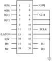
图4为一种RGB数据的组数为2,占空比支持1/16的动态扫描LED模块的20线接口布局,包括6位数据线R[1..0]、G[1..0]、B[1..0],1位移位时钟、1位行锁存信号/LATCH、1位开通信号/OE、4位行扫描信号H[3..0],有效的数据和控制信号线数为13,地线和空置管脚数为7。Figure 4 is a 20-line interface layout of a dynamic scanning LED module with a RGB data group number of 2 and a duty cycle that supports 1/16, including 6-bit data lines R[1..0], G[1..0 ], B[1..0], 1-bit shift clock, 1-bit line latch signal /LATCH, 1-bit enable signal /OE, 4-bit line scan signal H[3..0], effective data and control The number of signal lines is 13, and the number of ground wires and vacant pins is 7.
图5为一占空比为1/8,分辨率为32×16的动态LED模块的传统接口设计电路原理图,图中接口电路包括3片CMOS缓冲驱动芯片74HC245,1片CMOS 74HC138行译码器,1片CMOS 74HC123无信号关断保护芯片和两个20 P插座。其中:1片74HC245用于RGB输入数据的驱动,分2组R[]、G[]、B[]共6位分别输出到LED列驱动电路,作为上下两组RGB恒流芯片阵列的数据输入;1片74HC245用于控制信号的驱动,分2组SCLK、/LATCH、/OE信号共6位,一组CT[]输出到RGB恒流芯片去控制RGB数据的移位、锁存、开通和灰度显示,/OE还同时输出到CMOS74HC138去控制行切换时的行关断消隐,另一组CT_out输出到下一LED模块;1片74HC245用于行扫描信号的驱动,分2组行扫描信号共6位,一组输出H[]到本模块CMOS74HC138进行行译码,一组H_out输出到下一 LED模块;输入控制信号中的/LATCH还同时接入CMOS74HC123去实现无行扫描信号时的LED关断保护。这种并行的RGB数据和控制信号接口电路及采用的芯片74HC245、74HC138和74HC123流行多年,被各个公司广泛采用。其次,也有少数采用专用接口芯片的厂商,但处理的仍然是并行数据,这一点并未改变。Figure 5 is a traditional interface design circuit schematic diagram of a dynamic LED module with a duty ratio of 1/8 and a resolution of 32×16. The interface circuit in the figure includes 3 pieces of CMOS buffer driver chip 74HC245, and 1 piece of CMOS 74HC138 line decoding device, a CMOS 74HC123 no-signal shutdown protection chip and two 20 P sockets. Among them: 1 piece of 74HC245 is used to drive the RGB input data, divided into 2 groups of R[], G[], B[], a total of 6 bits are respectively output to the LED column drive circuit, as the data input of the upper and lower two groups of RGB constant current chip arrays ;One piece of 74HC245 is used to drive the control signal, divided into 2 groups of SCLK, /LATCH, /OE signals, a total of 6 bits, a group of CT[] output to the RGB constant current chip to control the shifting, latching, opening and closing of RGB data For grayscale display, /OE is also output to CMOS74HC138 to control the row off and blanking when switching rows, and another group of CT_out is output to the next LED module; 1 piece of 74HC245 is used for driving the row scanning signal, which is divided into 2 groups of row scanning The signal is 6 bits in total, a group of output H[] to this module CMOS74HC138 for row decoding, a group of H_out output to the next LED module; /LATCH in the input control signal is also connected to CMOS74HC123 to realize no row scanning signal LED shutdown protection. This parallel RGB data and control signal interface circuit and the chips 74HC245, 74HC138 and 74HC123 used have been popular for many years and have been widely used by various companies. Secondly, there are also a small number of manufacturers that use dedicated interface chips, but they still deal with parallel data, which has not changed.
由于在现有LED模块的信号接口电路设计中,各路RGB数据和控制信号一般均采用并行传送模式,它需要多片CMOS 74HC245作总线驱动器,动态扫描时还需要行译码器件74HC138作行译码。例如在占空比为1/4,分辨率为32列×16行的RGB全彩色LED模组设计中,RGB数据有12位,控制信号有5位,在传输速率为20MHz时,需要3片74HC245,一片74HC138,并采用20P插座和20芯扁平电缆,来完成RGB数据和LED扫描信号的缓冲驱动、译码和传送。该种现有技术虽然具有通用和利于各种LED模块的统一设计、便于采购和生产的优点,但是,却具有以下缺陷:1、该并行传送模式传送的数据和控制信号多达17位,连接线多,箱体布线显得繁杂;2、占用了较多FPGA的I/O资源;3、信号少时空脚多,显得不够经济;4、采用的接口芯片较多,不利于低密度LED显示屏的设计,且成本较高;5、由于尚无行业标准,迫使LED生产商开发出各种不同的HUB接口板来适应各公司不同LED模块的接口布局,增加了成本。Because in the signal interface circuit design of the existing LED module, each channel of RGB data and control signals generally adopts a parallel transmission mode, which requires multiple CMOS 74HC245 as a bus driver, and a line decoding device 74HC138 is also required for line decoding during dynamic scanning. code. For example, in the design of an RGB full-color LED module with a duty ratio of 1/4 and a resolution of 32 columns x 16 rows, the RGB data has 12 bits, and the control signal has 5 bits. When the transmission rate is 20MHz, 3 chips are required. 74HC245, a piece of 74HC138, and use 20P socket and 20-core flat cable to complete the buffer drive, decoding and transmission of RGB data and LED scanning signals. Although this prior art has the advantages of being universal and beneficial to the uniform design of various LED modules, and being convenient for procurement and production, it has the following defects: 1. The data and control signals transmitted by the parallel transmission mode are as many as 17 bits, and the connection There are many wires, and the wiring of the box is complicated; 2. It takes up more I/O resources of FPGA; 3. When there are few signals, there are many empty pins, which is not economical; 4. There are many interface chips used, which is not conducive to low-density LED display screens. 5. Since there is no industry standard yet, LED manufacturers are forced to develop various HUB interface boards to adapt to the interface layout of different LED modules of each company, which increases the cost.
发明内容Contents of the invention
本发明为了解决现有技术LED模块的信号接口电路存在连接线多、布线复杂、占用了较多FPGA的I/O资源且成本较高的技术问题,提供了一种LED模块的信号接口电路及LED显示装置。In order to solve the technical problems of the signal interface circuit of the LED module in the prior art, such as many connection lines, complicated wiring, taking up more I/O resources of the FPGA, and high cost, the present invention provides a signal interface circuit of the LED module and LED display device.
为解决上述技术问题,本发明采用的技术方案为设计一种LED模块的信号接口电路,包括LED点阵、与所述LED点阵连接的行驱动电路和列驱动电路,所述LED模块的信号接口电路还包括输入插座、输出插座、LVDS接口芯片和用于产生本地基准时钟的晶振,所述LVDS接口芯片具有:In order to solve the above technical problems, the technical solution adopted by the present invention is to design a signal interface circuit of an LED module, including an LED dot matrix, a row drive circuit and a column drive circuit connected to the LED dot matrix, and the signal interface circuit of the LED module The interface circuit also includes an input socket, an output socket, an LVDS interface chip and a crystal oscillator for generating a local reference clock, and the LVDS interface chip has:
用于接收RGB视频数据的数据差分输入端,其与所述输入插座连接;A data differential input terminal for receiving RGB video data, which is connected to the input socket;
用于输出RGB视频数据的数据差分输出端,其与所述输出插座连接; A data differential output terminal for outputting RGB video data, which is connected to the output socket;
用于接收本地基准时钟的本地时钟输入端,其与所述晶振的输出端连接;a local clock input terminal for receiving a local reference clock, which is connected to the output terminal of the crystal oscillator;
与所述列驱动电路连接且输出RGB数据至所述列驱动电路的RGB输出端;Connect with the column driver circuit and output RGB data to the RGB output end of the column driver circuit;
与所述列驱动电路连接且输出LED扫描控制信号至所述列驱动电路的LED扫描控制信号输出端;Connect with the column drive circuit and output the LED scan control signal to the LED scan control signal output end of the column drive circuit;
与所述行驱动电路连接且输出行扫描控制信号至所述行驱动电路的行扫描控制信号输出端; Connect with the row driver circuit and output the row scan control signal to the row scan control signal output end of the row driver circuit;
与数据差分输入端连接的Des/CDR模块,其接收所述数据差分输入端输入的RGB视频数据并从中恢复移位时钟且和数据位对齐,然后将数据差分输入端输入的RGB视频数据转换成并行数据输出;The Des/CDR module connected to the data differential input end, which receives the RGB video data input by the data differential input end and recovers the shift clock from it and aligns with the data bits, and then converts the RGB video data input by the data differential input end into parallel data output;
一根据本地时钟生成锁相时钟信号的锁相时钟生成模块;a phase-locked clock generating module that generates a phase-locked clock signal according to a local clock;
一输入端与所述Des/CDR模块、锁相时钟生成模块的输出端连接,输出端与所述RGB输出端、LED扫描控制信号输出端和行扫描控制信号输出端相连的RGB数据截取和控制信号生成模块,其接收所述Des/CDR模块输出的并行数据,并在所述恢复的移位时钟和所述锁相时钟的作用下完成并行数据的译码、缓冲、转换和对应LED模块的RGB视频数据的截取,并分别输出截取的RGB视频数据、LED扫描控制信号和行扫描控制信号至所述RGB输出端、LED扫描控制信号输出端和行扫描控制信号输出端,同时输出RGB视频数据;An input end is connected with the output end of the Des/CDR module and the phase-locked clock generation module, and the output end is connected with the RGB output end, the LED scan control signal output end and the line scan control signal output end. RGB data interception and control A signal generation module, which receives the parallel data output by the Des/CDR module, and completes the decoding, buffering, conversion of the parallel data and the corresponding LED module under the action of the recovered shift clock and the phase-locked clock Intercept RGB video data, and output the intercepted RGB video data, LED scan control signal and line scan control signal to the RGB output terminal, LED scan control signal output terminal and line scan control signal output terminal respectively, and output RGB video data at the same time ;
一与所述RGB数据截取和控制信号生成模块的输出端及数据差分输出端相接的串化器,所述串化器接收所述RGB数据截取和控制信号生成模块输出的RGB视频数据,并将接收到的RGB视频数据转换成串行数据输出至数据差分输出端。A serializer connected to the output end and the data differential output end of the RGB data interception and control signal generation module, the serializer receives the RGB video data output by the RGB data interception and control signal generation module, and The received RGB video data is converted into serial data and output to the data differential output terminal.
所述LVDS接口芯片还包括:The LVDS interface chip also includes:
一监控所述LED模块数据的信息采样模块;An information sampling module for monitoring the data of the LED module;
一接收下一LED模块数据的数据回传输入端;A data return input terminal for receiving the data of the next LED module;
一输出回传数据的数据回传输出端;- a data return output port that outputs return data;
一与所述数据回传输入端连接的回传Des/CDR模块,其接收所述数据回传输入端输入的下一LED模块数据,并转换成并行数据输出;A return Des/CDR module connected to the data return input end, which receives the next LED module data input by the data return input end, and converts it into parallel data output;
一与所述信息采样模块的输出端、回传Des/CDR模块的输出端连接且混合所述LED模块数据和下一LED模块数据的混合电路;A mixing circuit that is connected to the output of the information sampling module and the output of the return Des/CDR module and mixes the data of the LED module and the data of the next LED module;
一与混合电路的输出端连接的回传串化器,其将混合后的所述LED模块数据和下一LED模块数据转化成串行数据输出至数据回传输出端。A return serializer connected to the output end of the mixing circuit, which converts the mixed LED module data and the next LED module data into serial data and outputs it to the data return output end.
所述LVDS接口芯片还包括一与所述RGB数据截取和控制信号生成模块相连的FLASH存储器。The LVDS interface chip also includes a FLASH memory connected to the RGB data interception and control signal generation module.
所述晶振产生本地基准时钟。The crystal oscillator generates a local reference clock.
所述输入插座是2P插座。The input socket is a 2P socket.
所述输出插座是2P插座。The output socket is a 2P socket.
所述LVDS接口芯片的差分输入输出口支持热插拔功能。The differential input and output ports of the LVDS interface chip support a hot swap function.
所述Des/CDR模块模块包括CDR时钟数据恢复器和Des解串器。The Des/CDR module includes a CDR clock data restorer and a Des deserializer.
所述RGB视频数据流中含有LED模块控制信号和模块参数。The RGB video data stream contains LED module control signals and module parameters.
本发明还提供了一种具有上述LED模块的信号接口电路的LED显示装置。The present invention also provides an LED display device with the signal interface circuit of the above-mentioned LED module.
本发明还提供了一种用于LED模块的LVDS接口芯片,包括:The present invention also provides a kind of LVDS interface chip for LED module, comprising:
用于接收RGB视频数据的数据差分输入端;A data differential input terminal for receiving RGB video data;
用于输出RGB视频数据的数据差分输出端; A data differential output terminal for outputting RGB video data;
用于接收本地基准时钟的本地时钟输入端;a local clock input for receiving a local reference clock;
用于输出RGB数据的RGB输出端;RGB output terminal for outputting RGB data;
用于输出LED扫描控制信号的LED扫描控制信号输出端;An LED scanning control signal output terminal for outputting an LED scanning control signal;
用于输出行扫描控制信号的行扫描控制信号输出端; A row scan control signal output terminal for outputting a row scan control signal;
与数据差分输入端连接的Des/CDR模块,其接收所述数据差分输入端输入的RGB视频数据并从中恢复移位时钟且和数据位对齐,然后将数据差分输入端输入的RGB视频数据转换成并行数据输出;The Des/CDR module connected to the data differential input end, which receives the RGB video data input by the data differential input end and recovers the shift clock from it and aligns with the data bits, and then converts the RGB video data input by the data differential input end into parallel data output;
一根据本地基准时钟生成锁相时钟信号的锁相时钟生成模块;a phase-locked clock generating module that generates a phase-locked clock signal according to a local reference clock;
一输入端与所述Des/CDR模块、锁相时钟生成模块的输出端连接,输出端与所述RGB输出端、LED扫描控制信号输出端和行扫描控制信号输出端相连的RGB数据截取和控制信号生成模块,其接收所述Des/CDR模块输出的并行数据,并在所述恢复的移位时钟和所述锁相时钟的作用下完成并行数据的译码、缓冲、转换和对应LED模块的RGB视频数据的截取,并分别输出截取的RGB视频数据、LED扫描控制信号和行扫描控制信号至所述RGB输出端、LED扫描控制信号输出端和行扫描控制信号输出端,同时输出RGB视频数据;An input end is connected with the output end of the Des/CDR module and the phase-locked clock generation module, and the output end is connected with the RGB output end, the LED scan control signal output end and the line scan control signal output end. RGB data interception and control A signal generation module, which receives the parallel data output by the Des/CDR module, and completes the decoding, buffering, conversion of the parallel data and the corresponding LED module under the action of the recovered shift clock and the phase-locked clock Intercept RGB video data, and output the intercepted RGB video data, LED scan control signal and line scan control signal to the RGB output terminal, LED scan control signal output terminal and line scan control signal output terminal respectively, and output RGB video data at the same time ;
一与所述RGB数据截取和控制信号生成模块的输出端及数据差分输出端相接的串化器,所述串化器接收所述RGB数据截取和控制信号生成模块输出的RGB视频数据,并将接收到的RGB视频数据转换成串行数据输出至数据差分输出端。A serializer connected to the output end and the data differential output end of the RGB data interception and control signal generation module, the serializer receives the RGB video data output by the RGB data interception and control signal generation module, and The received RGB video data is converted into serial data and output to the data differential output terminal.
所述LVDS接口芯片还包括:The LVDS interface chip also includes:
一监控LED模块数据的信息采样模块;An information sampling module for monitoring the data of the LED module;
一接收下一LED模块数据的数据回传输入端;A data return input terminal for receiving the data of the next LED module;
一输出回传数据的数据回传输出端;- a data return output port that outputs return data;
一与所述数据回传输入端连接的回传Des/CDR模块,其接收所述数据回传输入端输入的下一LED模块数据,并转换成并行数据输出;A return Des/CDR module connected to the data return input end, which receives the next LED module data input by the data return input end, and converts it into parallel data output;
一与所述信息采样模块的输出端、回传Des/CDR模块的输出端连接且混合所述LED模块数据和下一LED模块数据的混合电路;A mixing circuit that is connected to the output of the information sampling module and the output of the return Des/CDR module and mixes the data of the LED module and the data of the next LED module;
一与混合电路的输出端连接的回传串化器,其将混合后的所述LED模块数据和下一LED模块数据转化成串行数据输出至数据回传输出端A return serializer connected to the output end of the mixing circuit, which converts the mixed LED module data and the next LED module data into serial data and outputs it to the data return output end
本发明通过设置LVDS接口芯片,只需要2根信号线即可实现LED模块全部数据和控制信号的缓冲驱动、译码和传送功能,连接线明显减少,箱体布线非常简单,而且大幅度减少了占用FPGA的I/O口资源,同时,采用的接口芯片少,有利于LED显示屏的设计,且有利于LED模块连接的标准化,成本也较低。By setting the LVDS interface chip, the present invention only needs 2 signal wires to realize the buffer drive, decoding and transmission functions of all data and control signals of the LED module, the connection wires are significantly reduced, the wiring of the cabinet is very simple, and the power consumption is greatly reduced. Occupies the I/O port resources of the FPGA, and at the same time, uses fewer interface chips, which is conducive to the design of LED display screens, and is conducive to the standardization of LED module connections, and the cost is also low.
附图说明Description of drawings
下面结合实施例和附图对本发明进行详细说明,其中:The present invention is described in detail below in conjunction with embodiment and accompanying drawing, wherein:
图1是本发明LED模块接口逻辑电路示意图;Fig. 1 is a schematic diagram of the interface logic circuit of the LED module of the present invention;
图2是本发明带监控回传功能的LED模块接口逻辑电路示意图Fig. 2 is a schematic diagram of the logic circuit of the interface of the LED module with monitoring and return function in the present invention
图3是本发明带监控回传功能的LVDS接口芯片逻辑电路设计示意图;Fig. 3 is a schematic diagram of the logic circuit design of the LVDS interface chip with the monitor return function of the present invention;
图4是现有LED模块20线接口示意图;Fig. 4 is a schematic diagram of the 20-wire interface of the existing LED module;
图5是现有LED模块接口逻辑电路示意图。Fig. 5 is a schematic diagram of an existing LED module interface logic circuit.
具体实施方式Detailed ways
纵观现代的数据通讯技术,我们不难发现,随着对信息流量需求的不断增长,传统并行接口技术已成为进一步提高数据传输速率的瓶颈。过去主要用于光纤通信的串行通信技术——SerDes正在取代传统并行总线而成为高速接口技术的主流。Looking at modern data communication technologies, it is not difficult to find that with the increasing demand for information flow, traditional parallel interface technology has become a bottleneck for further increasing data transmission rates. In the past, SerDes, a serial communication technology mainly used in optical fiber communication, is replacing the traditional parallel bus and becoming the mainstream of high-speed interface technology.
SERDES是并串行与串并行转换器SERializer/DESerializer(串化器/并化器)的缩写。有两种基本类型的SerDes接口:源同步(SS)协议和时钟数据恢复(CDR)协议。这两种类型的主要差别是如何实现时钟控制。源同步接口拥有一个伴随传送数据的时钟信号;CDR没有单独的时钟信号,而是把时钟嵌入在数据中。即CDR接收器将相位锁定在数据信号本身以获取时钟。SERDES is an abbreviation for parallel-serial and serial-parallel converter SERializer/DESerializer (serializer/parallelizer). There are two basic types of SerDes interfaces: source synchronous (SS) protocols and clock data recovery (CDR) protocols. The main difference between the two types is how clocking is implemented. A source-synchronous interface has a clock signal that accompanies the transmitted data; CDR does not have a separate clock signal, but embeds the clock in the data. i.e. the CDR receiver phase locks to the data signal itself to get the clock.
低压差分传送技术是基于低压差分信号LVDS(Low Voltage Differential Signal)的传送技术,LVDS接口又称RS644总线接口。LVDS是一种小振幅差分信号技术,它使用非常低的幅度信号,通过一对平行的PCB走线或平衡电缆传输数据。该传输标准采用恒流两线差分驱动模式,抗共模噪声干扰能力强,电磁辐射小,不会产生振铃和信号切换带来的尖峰信号,具有良好的EMI特性。还具有数据反转快、功耗低等优点。采用这种技术,只要保证平行传输线的长度足够一致,并在接收端提供良好的阻抗匹配减少信号反射,一对线就可以将数据的传输速率提高到800MHz以上,传输距离则随频率的增加而递减,可达几十米至几十厘米。由于LVDS具有这些优良特性,已广泛用于USB接口、 PCI Ex,都采用了差分式的数据传送方式。Low voltage differential transmission technology is based on low voltage differential signal LVDS (Low Voltage Differential Signal) transmission technology, LVDS interface is also called RS644 bus interface. LVDS is a small-amplitude differential signaling technology that uses very low-amplitude signals to transmit data over a pair of parallel PCB traces or balanced cables. This transmission standard adopts a constant current two-wire differential drive mode, which has strong anti-common-mode noise interference capability, low electromagnetic radiation, no ringing and peak signals caused by signal switching, and has good EMI characteristics. It also has the advantages of fast data reversal and low power consumption. Using this technology, as long as the length of parallel transmission lines is consistent enough, and good impedance matching is provided at the receiving end to reduce signal reflection, a pair of lines can increase the data transmission rate to above 800MHz, and the transmission distance increases with the increase of frequency. Decrease, up to tens of meters to tens of centimeters. Because LVDS has these excellent characteristics, it has been widely used in USB interface and PCI Ex, all of which adopt differential data transmission mode.
SerDes和低压差分传送技术具有卓越的性能,而SerDes IP和具有差分收发接口的可编程逻辑器件的出现与应用又为差分传送技术的应用创造了更有利的条件。目前,Altera、Xilinx、Actel等公司均推出了内部嵌有不等个数,速率为1.5-3.125G的SerDes IP核的 FPGA器件, 且这些FPGA器件IO口的输入输出都支持LVDS这种信号标准。高速串行差分传送技术的采用和支持高速串行差分传送技术器件的推出,无疑为实现高速的设备互连及组建大规模的电子系统提供了极大方便,从而推动了信息处理、视频显示、网络通讯和数据储存等领域的技术创新和跨越进步。SerDes and low-voltage differential transmission technology have excellent performance, and the emergence and application of SerDes IP and programmable logic devices with differential transceiver interfaces have created more favorable conditions for the application of differential transmission technology. At present, Altera, Xilinx, Actel and other companies have launched FPGA devices with different numbers of embedded SerDes IP cores with a rate of 1.5-3.125G, and the input and output of these FPGA device IO ports support the signal standard of LVDS . The adoption of high-speed serial differential transmission technology and the introduction of devices supporting high-speed serial differential transmission technology undoubtedly provide great convenience for realizing high-speed device interconnection and building large-scale electronic systems, thereby promoting information processing, video display, Technological innovation and leapfrog progress in the fields of network communication and data storage.
无独有偶,考察一下LED显示屏控制器控制技术的发展史,从数字分立器件到GAL、PAL,再到小规模FPGA直至大规模FPGA,无论是数字视频的采集、转换、传送、存储、分配,还是LED模组的扫描控制,正是基于以FPGA为核心构建,并随作FPGA的发展而发展。LED显示屏控制系统发送器的数据传送,尽管因成本因素尚未采用内部嵌有1.5-3.125G SerDes IP核的高档FPGA芯片,也在外部采用了SerDes和低压差分传送技术, 即通过FPGA的I/O口,将视频数据和控制信号并行输出到SerDes芯片。可以预见,随着高清视频和高分辨率视频应用的日益扩大,随作FPGA芯片的成本下降和价格的降低,内部嵌有SerDes IP核的FPGA芯片必将在LED显示屏的控制系统中占有一席之地。Coincidentally, examine the development history of LED display controller control technology, from digital discrete devices to GAL, PAL, to small-scale FPGA to large-scale FPGA, whether it is digital video collection, conversion, transmission, storage, distribution, or The scanning control of the LED module is based on FPGA as the core and develops with the development of FPGA. The data transmission of the LED display control system transmitter, although the high-end FPGA chip embedded with 1.5-3.125G SerDes IP core has not been adopted due to cost factors, SerDes and low-voltage differential transmission technology are also used externally, that is, through the I/O of the FPGA O port, which outputs video data and control signals to the SerDes chip in parallel. It can be foreseen that with the increasing application of high-definition video and high-resolution video, as the cost and price of FPGA chips decrease, FPGA chips with embedded SerDes IP cores will surely occupy a place in the control system of LED displays. .
然而,近20年间,LED模块间的数据流传输通讯技术,依然停止并局限于分离CMOS器件的应用而没有得到发展,模块之间的连接依然采用20线扁平电缆连接,模组的布局连接线多不简洁,用的芯片较多,体积偏大,成本偏高,尤其是应用于低密度屏时显得尤为突出,同时因公司而异的20线信号的杂乱分配,也不利于信号标准的建立和统一,不利于LED显示屏的高层次发展和进步。基于此,本发明提出一种采用SerDes通讯和低压差分传送技术的LED模块通讯芯片和电路设计方案, 通过内部设置有LVDS差分串行接口的专用芯片用于LED模组数据和控制信号的接入,它应用传输速率高达几百Mbps到几个Gbps的LVDS差分通讯信号,仅需1对双绞线即可实现LED模块间全部数据和控制信号的传送。同时利用内部的可编程逻辑资源,完成RGB数据的截取、LED控制信号的生成和输出。However, in the past 20 years, the data stream transmission communication technology between LED modules has still stopped and is limited to the application of separate CMOS devices and has not been developed. The connection between modules is still connected by 20-wire flat cables, and the layout of the modules It is not simple, it uses more chips, the volume is too large, and the cost is high, especially when it is applied to low-density screens. At the same time, the messy distribution of 20-line signals varies from company to company, which is not conducive to the establishment of signal standards. And unification is not conducive to the high-level development and progress of LED display screens. Based on this, the present invention proposes a LED module communication chip and circuit design scheme using SerDes communication and low-voltage differential transmission technology, and a dedicated chip with an internal LVDS differential serial interface is used for the access of LED module data and control signals , which uses LVDS differential communication signals with a transmission rate of several hundred Mbps to several Gbps, and only needs one pair of twisted pair to realize the transmission of all data and control signals between LED modules. At the same time, the internal programmable logic resources are used to complete the interception of RGB data, the generation and output of LED control signals.
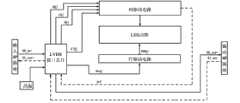
请参见图1、图2和图3,本发明LED模块的信号接口电路包括:LVDS接口芯片、晶振、输入2P插座和输出2P插座、LED点阵、与所述LED点阵连接的行驱动电路、与所述LED点阵连接的列驱动电路。晶振用于产生本地基准时钟。Please refer to Fig. 1, Fig. 2 and Fig. 3, the signal interface circuit of the LED module of the present invention includes: LVDS interface chip, crystal oscillator,
LVDS接口芯片包括:数据差分输入端、数据差分输出端、RGB输出端、LED扫描控制信号输出端、行扫描控制信号输出端、Des/CDR模块、锁相时钟生成模块、RGB数据截取和控制信号生成模块、串化器(Ser)和FLASH存储器。其中:LVDS interface chip includes: data differential input terminal, data differential output terminal, RGB output terminal, LED scanning control signal output terminal, line scanning control signal output terminal, Des/CDR module, phase-locked clock generation module, RGB data interception and control signal Build module, serializer (Ser) and FLASH memory. in:
数据差分输入端用于接收上一级LED模块或扫描控制器的RGB视频数据,其中,RGB视频数据中含有LED模块控制信号和模块参数。The data differential input terminal is used to receive the RGB video data of the upper-level LED module or scanning controller, wherein the RGB video data contains LED module control signals and module parameters.
数据差分输出端用于输出RGB视频数据至下一LED模块的LVDS接口芯片。The data differential output terminal is used to output RGB video data to the LVDS interface chip of the next LED module.
RGB输出端与所述LED列驱动电路相连,用于输出RGB数据至LED列驱动电路驱动LED灯工作。The RGB output terminal is connected to the LED row driving circuit for outputting RGB data to the LED row driving circuit to drive the LED lights to work.
本地时钟输入端与所述晶振相连,用于接收本地基准时钟;The local clock input terminal is connected to the crystal oscillator for receiving a local reference clock;
LED扫描控制信号输出端与所述LED列驱动电路相连,用于输出LED扫描控制信号至LED列驱动电路。The LED scanning control signal output terminal is connected with the LED row driving circuit for outputting the LED scanning control signal to the LED row driving circuit.
行扫描控制信号输出端与所述行驱动电路的输入端相连,用于输出行扫描控制信号至行驱动电路控制行驱动电路。The output terminal of the row scanning control signal is connected with the input terminal of the row driving circuit for outputting the row scanning control signal to the row driving circuit to control the row driving circuit.
Des/CDR模块与数据差分输入端连接,其接收所述数据差分输入端输入的RGB视频数据并从中恢复移位时钟且和数据位对齐,然后将数据差分输入端输入的RGB视频数据转换成并行数据输出。所述Des/CDR模块包括CDR时钟数据恢复器和Des解串器。The Des/CDR module is connected to the data differential input terminal, which receives the RGB video data input from the data differential input terminal and recovers the shift clock from it and aligns with the data bits, and then converts the RGB video data input from the data differential input terminal into parallel data output. The Des/CDR module includes a CDR clock data restorer and a Des deserializer.
锁相时钟生成模块根据本地时钟生成锁相时钟信号。The phase-locked clock generating module generates a phase-locked clock signal according to the local clock.
RGB数据截取和控制信号生成模块,其输入端与所述Des/CDR模块、锁相时钟生成模块的输出端连接,输出端与所述RGB输出端、LED扫描控制信号输出端、行扫描控制信号输出端和串化器相连。RGB数据截取和控制信号生成模块接收所述Des/CDR模块输出的并行数据,并在所述恢复的移位时钟和所述锁相时钟的作用下完成并行数据的译码、缓冲、转换和对应LED模块的RGB视频数据的截取,并分别输出截取的RGB视频数据、LED扫描控制信号和行扫描控制信号至所述RGB输出端、LED扫描控制信号输出端和行扫描控制信号输出端,同时输出RGB视频数据到串化器。RGB data interception and control signal generation module, its input end is connected with the output end of described Des/CDR module, phase-locked clock generation module, output end is connected with described RGB output end, LED scan control signal output end, row scan control signal The output terminal is connected to the serializer. The RGB data interception and control signal generation module receives the parallel data output by the Des/CDR module, and completes the decoding, buffering, conversion and correspondence of the parallel data under the action of the recovered shift clock and the phase-locked clock Intercepting the RGB video data of the LED module, and outputting the intercepted RGB video data, LED scanning control signal and line scanning control signal to the RGB output terminal, LED scanning control signal output terminal and line scanning control signal output terminal respectively, and simultaneously outputting RGB video data to serializer.
串化器(Ser)与所述RGB数据截取和控制信号生成模块的输出端及数据差分输出端相接。串化器接收所述RGB数据截取和控制信号生成模块输出的RGB视频数据,并将接收到的RGB视频数据转换成串行数据输出至数据差分输出端。The serializer (Ser) is connected to the output end and the data differential output end of the RGB data interception and control signal generation module. The serializer receives the RGB video data output by the RGB data interception and control signal generation module, converts the received RGB video data into serial data and outputs it to the data differential output terminal.
所述LVDS接口芯片的全部差分输入输出口支持热插拔功能。All differential input and output ports of the LVDS interface chip support a hot swap function.
FLASH存储器与所述RGB数据截取和控制信号生成模块相连,用于存储LED模块的参数。The FLASH memory is connected with the RGB data interception and control signal generation module for storing the parameters of the LED module.
输入2P(二针)插座与数据差分输入端相连,用以接收输入数据S0_in±。The
输出2P(二针)插座与所述数据差分输出端相连,用于输出S0_out±至下一LED模块的LVDS接口芯片。The
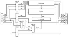
为了对LED灯的短路和开路、LED灯的校正系数、LED模块的温度及电压等信息进行监测,在接口部分的信号线增加虚线部分的LVDS差分数据输入S1_in±和输出S1_out±,以用于实现监控回传功能,同时LVDS接口芯片增加状态侦测、处理和回传功能。即LVDS接口芯片还包括:In order to monitor the short circuit and open circuit of the LED lamp, the correction coefficient of the LED lamp, the temperature and voltage of the LED module, etc., the LVDS differential data input S1_in± and output S1_out± of the dotted line are added to the signal line of the interface part for use in Realize the function of monitoring and returning, and at the same time, the LVDS interface chip increases the function of state detection, processing and returning. That is, the LVDS interface chip also includes:
信息采样模块,其监控所述LED模块数据;an information sampling module, which monitors the data of the LED module;
数据回传输入端,其接收下一LED模块数据S1_in±;Data return input terminal, which receives the next LED module data S1_in±;
数据回传输出端,其输出回传数据S1_out±;The data is transmitted back to the output terminal, and its output returns the data S1_out±;
回传Des/CDR模块,其与所述数据回传输入端连接,接收下一LED模块的回传数据,并转换成并行数据输出;Returning the Des/CDR module, which is connected to the data return input end, receives the return data of the next LED module, and converts it into parallel data output;
混合电路,其与所述信息采样模块的输出端、回传Des/CDR模块的输出端连接且混合所述LED模块数据和下一LED模块数据;A mixing circuit, which is connected to the output terminal of the information sampling module and the output terminal of the return Des/CDR module and mixes the data of the LED module and the data of the next LED module;
回传串化器(Ser),其与混合电路的输出端连接,将混合后的所述LED模块数据和下一LED模块数据转化成串行数据输出至数据回传输出端。A return serializer (Ser), which is connected to the output end of the mixing circuit, converts the mixed LED module data and the next LED module data into serial data and outputs it to the data return output end.
增加数据回传输出端和数据回传输入端后,由于增加了输入输出插口,所以在图2中将输入2P插座和输出2P插座分别改为输入4P插座和输出4P插座。After adding the data return output port and the data return input port, the
本发明LED模块的信号接口电路的工作原理为:差分数据输入S0_in±接收来自扫描控制板或上一LED模块的视频和系统控制数据,在CDR接收器的作用下锁相恢复移位时钟,并和数据位对齐,再通过Des(Deserializes ,并化器)8B/10B解码、串并转换后输出到RGB数据截取和扫描控制信号发生器;RGB数据截取和扫描控制信号发生模块在接收时钟和本地锁相时钟的作用下完成原始数据的译码、缓冲、转换和本LED模块RGB[]视频数据的截取,再通过RGB数据截取和扫描控制信号发生模块内置的扫描控制信号发生电路生成LED扫描控制信号CT[],包括移位时钟SCLK、数据锁存信号/LATCH、灰度门控信号/EN和已译码的行扫描信号Ho[7..0],并通过并行口驱动输出以实现RGB数据的视频显示,同时原始数据通过Ser(Serializes,串化器) 8B/10B编码和串化处理,再嵌入PLL锁相环时钟后经差分数据输出S0_out±连接到下一级LED模块。The working principle of the signal interface circuit of the LED module of the present invention is: the differential data input S0_in ± receives the video and system control data from the scanning control board or the previous LED module, phase-locks and restores the shift clock under the action of the CDR receiver, and Align with the data bits, and then through Des (Deserializes, parallelizer) 8B/10B decoding, serial-to-parallel conversion, and then output to the RGB data interception and scanning control signal generator; the RGB data interception and scanning control signal generation module receives the clock and the local Under the action of the phase-locked clock, the decoding, buffering, conversion of the original data and the interception of the RGB[] video data of this LED module are completed, and then the LED scanning control is generated through the RGB data interception and the scanning control signal generation circuit built in the scanning control signal generation module. Signal CT[], including shift clock SCLK, data latch signal /LATCH, grayscale gate control signal /EN and decoded row scanning signal Ho[7..0], and drives output through parallel port to realize RGB The video display of the data, at the same time, the original data is encoded and serialized by Ser (Serializes, serializer) 8B/10B, and then embedded in the PLL phase-locked loop clock, and then connected to the next-level LED module through the differential data output S0_out±.
LVDS信号接口芯片的并行输出口可这样设计,显示数据输出R[3..0]、G[3..0]、B[3..0]共四组RGB数据,其输出功能可通过软件编程,除支持1-4组数据结构的各种LED模块外,采用R[3..0]、G[1..0]、B[1..0]数据结构支持虚拟像素显示;采用R[0]、G[0]、B[0]单组数据结构,剩余的R[3..1]、G[3..1]、B[3..1]的8位可作为1/16动态扫描的高位行扫描线;采用R[1..0]、G[1..0]、B[1..0]2组数据结构,剩余的R[3..2]、G[3..2]、B[3..2]可作为多分枝LED扫描控制信号SCLK、数据锁存信号/LATCH和灰度门控信号/EN输出,以方便LED模块设计。固定的行扫描信号则为Ho[7..0]共8位,支持1/2、1/4、1/8动态扫描显示和静态显示,同时可通过编程实现1/3、1/5、1/6和1/7任意占空比的动态扫描显示。The parallel output port of the LVDS signal interface chip can be designed in this way, display data output R[3..0], G[3..0], B[3..0] a total of four groups of RGB data, and its output function can be controlled by software Programming, in addition to supporting various LED modules with 1-4 sets of data structures, use R[3..0], G[1..0], B[1..0] data structures to support virtual pixel display; use R [0], G[0], B[0] single group data structure, the remaining 8 bits of R[3..1], G[3..1], B[3..1] can be used as 1/ 16 high-level row scan lines for dynamic scanning; use R[1..0], G[1..0], B[1..0] 2 data structures, and the remaining R[3..2], G[ 3..2], B[3..2] can be output as multi-branch LED scan control signal SCLK, data latch signal /LATCH and grayscale gate control signal /EN to facilitate LED module design. The fixed line scan signal is Ho[7..0] with a total of 8 bits, which supports 1/2, 1/4, 1/8 dynamic scan display and static display, and can be programmed to realize 1/3, 1/5, Dynamic scanning display of 1/6 and 1/7 arbitrary duty cycle.
在接口芯片中嵌入信息采样模块可完成本级LED模块监控数据S[]的获取,差分数据输入S1_in±接收来自下一LED模块的监测数据, 经Des解串后通过混合模块与本级模块的监测信号混合,再到输入端的Ser串化编码,经输入端的差分数据输出传往上一级LED模块或扫描控制板。Embedding the information sampling module in the interface chip can complete the acquisition of the monitoring data S[] of the LED module at the current level. The differential data input S1_in± receives the monitoring data from the next LED module. The monitoring signal is mixed, and then to the Ser serialization coding at the input end, and then transmitted to the upper-level LED module or scanning control board through the differential data output at the input end.
在接口芯片中嵌入的FLASH模块用于存储本级LED模块参数、RGB校正数据和其它有用的信息,用于亮度、色度的像素校正和智能控制。The FLASH module embedded in the interface chip is used to store the parameters of the current LED module, RGB correction data and other useful information for pixel correction and intelligent control of brightness and chromaticity.
当不采用回传监测功能时,去掉图5虚线部分,即为成本较低的单对差分线传送方案。When the backhaul monitoring function is not used, remove the dotted line in Figure 5, which is a low-cost single-pair differential line transmission solution.
至于LVDS信号接口芯片的封装,可以采用微型TQFP封装、QFN封装,如采用BGA封装,则在四层板的LED模块设计中更具有优势。As for the packaging of the LVDS signal interface chip, micro TQFP packaging and QFN packaging can be used. If BGA packaging is used, it has more advantages in the design of LED modules with four-layer boards.
本发明LED模块的信号接口电路可用于各种LED显示装置,如单色LED显示屏、双基LED显示屏、全彩LED显示屏等。The signal interface circuit of the LED module of the present invention can be used in various LED display devices, such as single-color LED display screens, dual-base LED display screens, full-color LED display screens, and the like.
本发明具有如下优点: The present invention has the following advantages:
1、采用1条高速LVDS串行链路,仅需2根信号线,即可实现LED模块全部数据和控制信号的缓冲驱动、译码和传送功能。1. Using one high-speed LVDS serial link, only two signal lines are needed to realize the buffer drive, decoding and transmission functions of all data and control signals of the LED module.
2、利用芯片的内部资源完成LED模块的数据及控制信号的截取、驱动和译码,同时支持虚拟像素显示、1--16行动态扫描或静态驱动。2. Use the internal resources of the chip to complete the interception, driving and decoding of the data and control signals of the LED module, and support virtual pixel display, 1--16 lines of dynamic scanning or static driving.
3、性能优异,通信速率可高达270Mbps到3.125Gbps,传输数据量大、抗干扰性好、可靠性高,LVDS 数据速率可高达270Mbps到3.125Gbps, 同时分离CMOS芯片被集成的接口芯片所代替,相比现有技术其电路大大简化。3. Excellent performance, the communication rate can be as high as 270Mbps to 3.125Gbps, the transmission data volume is large, the anti-interference performance is good, and the reliability is high. The LVDS data rate can be as high as 270Mbps to 3.125Gbps. At the same time, the separated CMOS chip is replaced by the integrated interface chip. Compared with the prior art, its circuit is greatly simplified.
4、它大幅度减少了LED模块间信号连接线的数量,使LED箱体布线设计更简洁,成本降低。4. It greatly reduces the number of signal connection lines between LED modules, making the wiring design of the LED cabinet more concise and reducing the cost.
5、输出管脚的功能可由用户自行定义编程,这给PCB板的设计带来了灵活性。5. The function of the output pin can be defined and programmed by the user, which brings flexibility to the design of the PCB board.
6、扩充1条LVDS串行回传链路,具有信号监测功能,提高了LED显示屏的应用等级。6. Expand one LVDS serial backhaul link, with signal monitoring function, which improves the application level of LED display.
7、大幅度减少扫描控制板FPGA的I/O口输出,允许采用更小封装的FPGA或更简单的器件,进一步降低了成本。7. Significantly reduce the I/O port output of the scanning control board FPGA, allowing the use of smaller packaged FPGAs or simpler devices, further reducing costs.
8、有利于LED模块连接和通讯协议的标准化工作。8. It is conducive to the standardization of LED module connection and communication protocols.
以上所述仅为本发明的较佳实施例而已,并不用以限制本发明,凡在本发明的精神和原则之内所作的任何修改、等同替换和改进,例如将单对差分视频输入改为两对差分视频输入等,均应包含在本发明的保护范围之内。 The above description is only a preferred embodiment of the present invention, and is not intended to limit the present invention. Any modifications, equivalent replacements and improvements made within the spirit and principles of the present invention, such as changing the single-pair differential video input to Two pairs of differential video inputs, etc., should be included in the protection scope of the present invention. the
Claims (10)
Translated fromChinesePriority Applications (1)
| Application Number | Priority Date | Filing Date | Title |
|---|---|---|---|
| CN201110103831.8ACN102760403B (en) | 2011-04-25 | 2011-04-25 | A kind of signal interface circuit of LED module and LED display |
Applications Claiming Priority (1)
| Application Number | Priority Date | Filing Date | Title |
|---|---|---|---|
| CN201110103831.8ACN102760403B (en) | 2011-04-25 | 2011-04-25 | A kind of signal interface circuit of LED module and LED display |
Publications (2)
| Publication Number | Publication Date |
|---|---|
| CN102760403Atrue CN102760403A (en) | 2012-10-31 |
| CN102760403B CN102760403B (en) | 2015-10-28 |
Family
ID=47054850
Family Applications (1)
| Application Number | Title | Priority Date | Filing Date |
|---|---|---|---|
| CN201110103831.8AExpired - Fee RelatedCN102760403B (en) | 2011-04-25 | 2011-04-25 | A kind of signal interface circuit of LED module and LED display |
Country Status (1)
| Country | Link |
|---|---|
| CN (1) | CN102760403B (en) |
Cited By (12)
| Publication number | Priority date | Publication date | Assignee | Title |
|---|---|---|---|---|
| CN103426402A (en)* | 2013-08-09 | 2013-12-04 | 深圳市奥拓电子股份有限公司 | LED (light-emitting diode) display system, display module thereof and data transmission method |
| CN103841693A (en)* | 2012-11-21 | 2014-06-04 | 欧普照明股份有限公司 | Constant current drive circuit and LED light source lighting circuit with constant current drive circuit |
| CN105321465A (en)* | 2015-10-27 | 2016-02-10 | 刘志海 | LED display screen control system based on FPGA module |
| CN106847166A (en)* | 2017-02-14 | 2017-06-13 | 江苏利鼎微系统有限公司 | A kind of one of small spacing all-colour LED display module 128 scan method |
| CN107358908A (en)* | 2017-05-22 | 2017-11-17 | 福建祥云光电科技有限公司 | A kind of P5.75 patterns LED display |
| CN107424557A (en)* | 2017-08-16 | 2017-12-01 | 深圳市德普微电子有限公司 | A kind of single dual-colored LED display drive circuit |
| CN109616066A (en)* | 2018-12-29 | 2019-04-12 | 惠科股份有限公司 | Signal generating circuit and display device using same |
| WO2020041939A1 (en)* | 2018-08-27 | 2020-03-05 | 西安诺瓦电子科技有限公司 | Display control system |
| CN113012633A (en)* | 2021-03-02 | 2021-06-22 | 深圳高鼎通信息技术有限公司 | Point-to-point correction system of common-sun LED display screen and implementation method thereof |
| CN115602097A (en)* | 2021-07-08 | 2023-01-13 | 西安钛铂锶电子科技有限公司(Cn) | Interface chip and display device |
| CN115602096A (en)* | 2021-07-07 | 2023-01-13 | 西安钛铂锶电子科技有限公司(Cn) | Interface chip, display module and display cabinet |
| CN115604417A (en)* | 2021-07-08 | 2023-01-13 | 西安钛铂锶电子科技有限公司(Cn) | Interface chip and display module |
Citations (6)
| Publication number | Priority date | Publication date | Assignee | Title |
|---|---|---|---|---|
| JP2003101975A (en)* | 2001-09-26 | 2003-04-04 | Canon Inc | Multi-tone transmission method |
| JP2005260620A (en)* | 2004-03-12 | 2005-09-22 | Fuji Xerox Co Ltd | Image processor and its data transmitting method |
| CN1964465A (en)* | 2006-11-22 | 2007-05-16 | 天津亚威达电子有限公司 | A FPGA-based video image processor |
| CN101192371A (en)* | 2006-11-28 | 2008-06-04 | 康佳集团股份有限公司 | LEDLED display module group signal |
| CN201622783U (en)* | 2009-12-22 | 2010-11-03 | 康佳集团股份有限公司 | LED module communication circuit and LED display screen |
| CN201773567U (en)* | 2010-04-26 | 2011-03-23 | 苏州长风有限责任公司 | LVDS signal encoding circuit for display |
- 2011
- 2011-04-25CNCN201110103831.8Apatent/CN102760403B/ennot_activeExpired - Fee Related
Patent Citations (6)
| Publication number | Priority date | Publication date | Assignee | Title |
|---|---|---|---|---|
| JP2003101975A (en)* | 2001-09-26 | 2003-04-04 | Canon Inc | Multi-tone transmission method |
| JP2005260620A (en)* | 2004-03-12 | 2005-09-22 | Fuji Xerox Co Ltd | Image processor and its data transmitting method |
| CN1964465A (en)* | 2006-11-22 | 2007-05-16 | 天津亚威达电子有限公司 | A FPGA-based video image processor |
| CN101192371A (en)* | 2006-11-28 | 2008-06-04 | 康佳集团股份有限公司 | LEDLED display module group signal |
| CN201622783U (en)* | 2009-12-22 | 2010-11-03 | 康佳集团股份有限公司 | LED module communication circuit and LED display screen |
| CN201773567U (en)* | 2010-04-26 | 2011-03-23 | 苏州长风有限责任公司 | LVDS signal encoding circuit for display |
Cited By (16)
| Publication number | Priority date | Publication date | Assignee | Title |
|---|---|---|---|---|
| CN103841693A (en)* | 2012-11-21 | 2014-06-04 | 欧普照明股份有限公司 | Constant current drive circuit and LED light source lighting circuit with constant current drive circuit |
| CN103841693B (en)* | 2012-11-21 | 2017-02-15 | 欧普照明股份有限公司 | Constant current drive circuit and LED light source lighting circuit with constant current drive circuit |
| CN103426402A (en)* | 2013-08-09 | 2013-12-04 | 深圳市奥拓电子股份有限公司 | LED (light-emitting diode) display system, display module thereof and data transmission method |
| CN105321465A (en)* | 2015-10-27 | 2016-02-10 | 刘志海 | LED display screen control system based on FPGA module |
| CN106847166B (en)* | 2017-02-14 | 2020-11-27 | 江苏利鼎微系统有限公司 | A scanning method for small-pitch full-color LED display module 128 |
| CN106847166A (en)* | 2017-02-14 | 2017-06-13 | 江苏利鼎微系统有限公司 | A kind of one of small spacing all-colour LED display module 128 scan method |
| CN107358908A (en)* | 2017-05-22 | 2017-11-17 | 福建祥云光电科技有限公司 | A kind of P5.75 patterns LED display |
| CN107424557A (en)* | 2017-08-16 | 2017-12-01 | 深圳市德普微电子有限公司 | A kind of single dual-colored LED display drive circuit |
| CN107424557B (en)* | 2017-08-16 | 2023-01-24 | 深圳市德普微电子有限公司 | Single-double-color LED display screen driving circuit |
| WO2020041939A1 (en)* | 2018-08-27 | 2020-03-05 | 西安诺瓦电子科技有限公司 | Display control system |
| CN109616066B (en)* | 2018-12-29 | 2020-12-11 | 惠科股份有限公司 | Signal generating circuit and display device using same |
| CN109616066A (en)* | 2018-12-29 | 2019-04-12 | 惠科股份有限公司 | Signal generating circuit and display device using same |
| CN113012633A (en)* | 2021-03-02 | 2021-06-22 | 深圳高鼎通信息技术有限公司 | Point-to-point correction system of common-sun LED display screen and implementation method thereof |
| CN115602096A (en)* | 2021-07-07 | 2023-01-13 | 西安钛铂锶电子科技有限公司(Cn) | Interface chip, display module and display cabinet |
| CN115602097A (en)* | 2021-07-08 | 2023-01-13 | 西安钛铂锶电子科技有限公司(Cn) | Interface chip and display device |
| CN115604417A (en)* | 2021-07-08 | 2023-01-13 | 西安钛铂锶电子科技有限公司(Cn) | Interface chip and display module |
Also Published As
| Publication number | Publication date |
|---|---|
| CN102760403B (en) | 2015-10-28 |
Similar Documents
| Publication | Publication Date | Title |
|---|---|---|
| CN102760403B (en) | A kind of signal interface circuit of LED module and LED display | |
| CN205158877U (en) | LED display control card, LED lamp plate and LED display system | |
| CN105141877B (en) | A kind of chromacoder based on programming device | |
| CN102760402B (en) | The signal interface circuit of a kind of LED module and LED display | |
| CN111063287B (en) | Display control system | |
| CN108345553B (en) | Satellite-borne high-resolution imaging data transmission and acquisition system | |
| CN111063285B (en) | Display control system and display unit board | |
| CN201130518Y (en) | LED data scanning board | |
| CN102917213A (en) | System and method for transmitting optical fiber video images | |
| CN113852775A (en) | Image data transmission device and method, and nonvolatile storage medium | |
| CN101378483A (en) | Digital high clear display control device and method | |
| TWM650787U (en) | Control system for led display and display device | |
| CN201773567U (en) | LVDS signal encoding circuit for display | |
| CN100507997C (en) | A signal interconnection method of LED display screen | |
| CN105118409B (en) | V BY ONE coding/decoding systems and method based on FPGA | |
| CN115691346A (en) | Display screen, display system and display box | |
| CN212381303U (en) | Device for realizing double-link DVI (digital video interactive) based on FPGA (field programmable Gate array) | |
| CN204948223U (en) | A kind of chromacoder based on programming device | |
| CN102740128B (en) | A kind of video transmission device and its implementation with function of surfing the Net | |
| CN201622783U (en) | LED module communication circuit and LED display screen | |
| CN111818699A (en) | Control method and control circuit of RGB-LED light source | |
| CN200947337Y (en) | LED full chromatic display screen control system | |
| CN111063286B (en) | Display control system and display unit board | |
| TWI819762B (en) | Millimeter wave wireless connector chips, wireless connectors and signal transmission systems | |
| CN211239967U (en) | Display controller, display control system and LED display system |
Legal Events
| Date | Code | Title | Description |
|---|---|---|---|
| C06 | Publication | ||
| PB01 | Publication | ||
| C10 | Entry into substantive examination | ||
| SE01 | Entry into force of request for substantive examination | ||
| C14 | Grant of patent or utility model | ||
| GR01 | Patent grant | ||
| CF01 | Termination of patent right due to non-payment of annual fee | ||
| CF01 | Termination of patent right due to non-payment of annual fee | Granted publication date:20151028 |