CN102751871A - Switching power supply device - Google Patents
Switching power supply deviceDownload PDFInfo
- Publication number
- CN102751871A CN102751871ACN2012101345537ACN201210134553ACN102751871ACN 102751871 ACN102751871 ACN 102751871ACN 2012101345537 ACN2012101345537 ACN 2012101345537ACN 201210134553 ACN201210134553 ACN 201210134553ACN 102751871 ACN102751871 ACN 102751871A
- Authority
- CN
- China
- Prior art keywords
- switching element
- voltage
- power supply
- switching
- supply device
- Prior art date
- Legal status (The legal status is an assumption and is not a legal conclusion. Google has not performed a legal analysis and makes no representation as to the accuracy of the status listed.)
- Granted
Links
Images


Classifications
- H—ELECTRICITY
- H02—GENERATION; CONVERSION OR DISTRIBUTION OF ELECTRIC POWER
- H02M—APPARATUS FOR CONVERSION BETWEEN AC AND AC, BETWEEN AC AND DC, OR BETWEEN DC AND DC, AND FOR USE WITH MAINS OR SIMILAR POWER SUPPLY SYSTEMS; CONVERSION OF DC OR AC INPUT POWER INTO SURGE OUTPUT POWER; CONTROL OR REGULATION THEREOF
- H02M3/00—Conversion of DC power input into DC power output
- H02M3/02—Conversion of DC power input into DC power output without intermediate conversion into AC
- H02M3/04—Conversion of DC power input into DC power output without intermediate conversion into AC by static converters
- H02M3/10—Conversion of DC power input into DC power output without intermediate conversion into AC by static converters using discharge tubes with control electrode or semiconductor devices with control electrode
- H02M3/145—Conversion of DC power input into DC power output without intermediate conversion into AC by static converters using discharge tubes with control electrode or semiconductor devices with control electrode using devices of a triode or transistor type requiring continuous application of a control signal
- H02M3/155—Conversion of DC power input into DC power output without intermediate conversion into AC by static converters using discharge tubes with control electrode or semiconductor devices with control electrode using devices of a triode or transistor type requiring continuous application of a control signal using semiconductor devices only
- H02M3/156—Conversion of DC power input into DC power output without intermediate conversion into AC by static converters using discharge tubes with control electrode or semiconductor devices with control electrode using devices of a triode or transistor type requiring continuous application of a control signal using semiconductor devices only with automatic control of output voltage or current, e.g. switching regulators
- H02M3/158—Conversion of DC power input into DC power output without intermediate conversion into AC by static converters using discharge tubes with control electrode or semiconductor devices with control electrode using devices of a triode or transistor type requiring continuous application of a control signal using semiconductor devices only with automatic control of output voltage or current, e.g. switching regulators including plural semiconductor devices as final control devices for a single load
Landscapes
- Engineering & Computer Science (AREA)
- Power Engineering (AREA)
- Dc-Dc Converters (AREA)
Abstract
Translated fromChinese
Description
Translated fromChinese技术领域technical field
本发明涉及一种通过开关动作来生成并输出规定电压的开关电源(switching power supply)装置。The present invention relates to a switching power supply (switching power supply) device that generates and outputs a prescribed voltage through switching operations.
背景技术Background technique
近年来,在信息设备、家电设备等各种设备中广泛利用着开关电源装置。尤其是在移动终端装置等信息设备中,需要针对CPU(Central ProcessingUnit,中央处理器)驱动用、显示器驱动用、通信接口用等对应不同功能供给不同电压的各种电源,且必须利用电池电源(也就是输入电压)生成这些电源(也就是输出电压)。由于开关电源可通过使要施加于线圈的电压在接通/断开之间切换而获得所需的输出电压,因而得到广泛应用。In recent years, switching power supply devices have been widely used in various equipment such as information equipment and home appliances. Especially in information equipment such as mobile terminal devices, it is necessary to supply various power sources of different voltages for different functions such as CPU (Central Processing Unit, central processing unit) drive, display drive, and communication interface, and battery power ( That is, the input voltage) generates these power supplies (that is, the output voltage). Since the switching power supply can obtain a desired output voltage by switching the voltage to be applied to the coil on/off, it is widely used.
作为该开关电源的一例,例如在专利文献1中公开有如下技术:在临界模式PFC(Power Factor Correction,功率因数修正)升压型转换器中,检测输入电压及输出电压,并使用所检测出的这些电压进行规定的运算,由此决定开关元件的接通持续时间(duration)及断开持续时间,并基于所决定的接通持续时间及断开持续时间,使开关元件接通/断开。As an example of this switching power supply, for example, Patent Document 1 discloses the following technology: In a critical mode PFC (Power Factor Correction, power factor correction) boost converter, the input voltage and the output voltage are detected, and the detected voltage is used. These voltages perform prescribed calculations, thereby determining the on-duration and off-duration of the switching element, and based on the determined on-duration and off-duration, the switching element is turned on/off .
在这种开关电源装置中,为了有效率地进行稳定的电源供给,在适宜的时刻进行切换成为共通的课题。In such a switching power supply device, in order to efficiently supply a stable power supply, switching at an appropriate timing is a common problem.
(现有技术文献)(Prior art literature)
专利文献1:日本国专利申请公开公报“特开2010-104218号公报”;2010年5月6日公开。Patent Document 1: Japanese Patent Application Publication "JP-A-2010-104218"; published on May 6, 2010.
发明内容Contents of the invention
然而,在以往的开关电源装置中,因为是通过规定的运算来决定开关元件的接通时刻,所以如果该运算中产生误差,那么开关元件的接通时刻中也会产生偏差。另外,适宜的接通时刻会根据开关元件的端子间电容、线圈的电感值、输入电压等可变因素而变动,在以往的开关电源装置中,因为通过规定的运算来决定开关元件的接通时刻,所以无法应对所述可变因素。因此,在以往的开关电源装置中,无法在适宜的时刻使开关元件接通。However, in the conventional switching power supply device, since the ON timing of the switching element is determined by a predetermined calculation, if an error occurs in the calculation, a deviation occurs in the ON timing of the switching element. In addition, the appropriate turn-on timing varies depending on variable factors such as the capacitance between the terminals of the switching element, the inductance value of the coil, and the input voltage. In conventional switching power supply devices, the turn-on of the switching element is determined by a predetermined calculation moment, so cannot cope with said variable factors. Therefore, in the conventional switching power supply device, the switching element cannot be turned on at an appropriate timing.
因此,本发明是鉴于所述问题而完成,目的在于提供一种开关电源装置,可以使用于切换对线圈是否施加电压的开关元件的接通时刻进一步优化。Therefore, the present invention was made in view of the above problems, and an object of the present invention is to provide a switching power supply device that can further optimize the turn-on timing of a switching element for switching whether or not to apply a voltage to a coil.
为了解决所述课题,本发明的开关电源装置是通过与线圈的一端相连接的开关元件来在是否对所述线圈施加直流电压间进行切换,且使在开关元件接通期间蓄积在所述线圈中的磁能作为由开关元件断开期间在所述线圈中流通的电流传输的电能而提取到输出侧,从而获得输出电压;该开关电源装置的特征在于:所述开关元件包含互相共源共栅连接(cascodeconnection)的常导通型的第1开关元件及常断开型的第2开关元件;且所述开关电源装置包括:电压检测单元,检测所述开关元件的共源共栅连接点上的电压;以及控制单元,根据由所述电压检测单元所检测出的所述电压,控制所述开关元件的接通。In order to solve the above-mentioned problems, the switching power supply device of the present invention switches whether or not to apply a DC voltage to the coil through a switching element connected to one end of the coil, and makes the voltage accumulated in the coil when the switching element is turned on. The magnetic energy in the switch element is extracted to the output side as the electric energy transmitted by the current flowing in the coil during the switch-off period, thereby obtaining the output voltage; the switching power supply device is characterized in that the switch elements include mutual cascode A normally-on type first switching element and a normally-off type second switching element connected (cascodeconnection); and the switching power supply device includes: a voltage detection unit that detects the cascode connection point a voltage; and a control unit that controls turning on of the switching element according to the voltage detected by the voltage detection unit.
根据该结构,因为是根据决定开关元件的适宜的接通时刻的开关元件的共源共栅连接点上的电压来控制开关元件的接通,所以即便在如根据开关元件的端子间电容、电感值、或输入电压,而使线圈电流变为0后直至开关元件的汲极电压降至规定电压为止的时间差发生变动的情况下,也不会在汲极电压降至规定电压之前使开关元件接通。因此,可以使开关元件的接通时刻进一步最佳化。另外,通过检测开关元件彼此的共源共栅连接点的电位,而可利用低于开关元件的端子间电压的电压来控制开关元件的接通时刻。According to this configuration, since the on-on of the switching element is controlled based on the voltage at the cascode connection point of the switching element that determines the appropriate on-time of the switching element, even if the switching element is controlled by the inter-terminal capacitance and inductance of the switching element, value, or input voltage, and when the time difference between the coil current becomes 0 and the drain voltage of the switching element drops to the specified voltage varies, the switching element will not be connected before the drain voltage drops to the specified voltage. Pass. As a result, the turn-on timing of the switching element can be further optimized. In addition, by detecting the potential of the cascode connection point between the switching elements, it is possible to control the turn-on timing of the switching elements with a voltage lower than the inter-terminal voltage of the switching elements.
通常,随着检测部中的耐压变大,检测部的成本会增加。另外,随着检测部中的耐压范围扩大,检测部的检测精度会降低。在此,本发明采用的技术方案是对共源共栅连接点的电压进行检测,由此根据该技术方案,而检测更低的电压。由此,可以抑制检测部的成本,而且可以提高检测部的检测精度。Generally, as the withstand voltage in the detection part becomes larger, the cost of the detection part increases. In addition, as the withstand voltage range in the detection part increases, the detection accuracy of the detection part decreases. Here, the technical solution adopted by the present invention is to detect the voltage of the cascode connection point, so that a lower voltage is detected according to the technical solution. Accordingly, the cost of the detection unit can be suppressed, and the detection accuracy of the detection unit can be improved.
于此,如果仅使检测部中的电压降低,那么也可以考虑通过电阻来进行分压的技术方案,但在此情况下,零件件数会增加,而且会产生电阻所致的导通损耗。本发明由于并未采用这种技术方案,所以零件件数不会增加,也不会产生导通损耗。Here, if only the voltage in the detection part is lowered, it is conceivable to divide the voltage by resistors, but in this case, the number of components increases and conduction loss due to resistors occurs. Since the present invention does not adopt this technical solution, the number of parts will not increase, and conduction loss will not occur.
[发明效果][Invention effect]
根据本发明的开关电源装置,发挥能够使用于在是否对线圈施加电压间进行切换的开关元件的接通时刻进一步最佳化这样的效果。According to the switching power supply device of the present invention, it is possible to further optimize the turn-on timing of the switching element for switching whether or not to apply a voltage to the coil.
附图说明Description of drawings
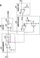
图1表示本实施方式的开关电源装置的结构。FIG. 1 shows the configuration of a switching power supply device according to this embodiment.
图2表示本实施方式的开关电源装置所包含的控制单元的详细结构。FIG. 2 shows a detailed configuration of a control unit included in the switching power supply device of the present embodiment.
图3表示本实施方式的开关电源装置执行动作时的各种参数的波形。FIG. 3 shows waveforms of various parameters when the switching power supply device of this embodiment operates.
[附图标记说明][Description of Reference Signs]
100 开关电源装置100 switching power supply unit
200 控制电路(控制单元)200 control circuit (control unit)
210 底部电压检测电路210 Bottom voltage detection circuit
220 驱动电路220 drive circuit
230 误差放大电路230 error amplifier circuit
240 接通时刻生成电路240 Turn-on moment generating circuit
C1 电容器C1 capacitor
C2 电容器C2 capacitor
C3 电容器C3 capacitor
D1 二极管D1 diode
L1 线圈L1 Coil
Q1 开关元件Q1 switching element
Q1A 开关元件(第1开关元件)Q1A Switching element (1st switching element)
Q1B 开关元件(第2开关元件)Q1B switching element (second switching element)
R11 电阻R11 resistor
R12 电阻R12 resistor
具体实施方式Detailed ways
下面,参照附图说明本发明的实施方式。图1表示本实施方式的开关电源装置100的结构。电源装置100是所谓的升压型开关电源装置,即,通过与线圈L1的一端相连接的开关元件Q1,来在对线圈L1是否施加直流电压之间切换,且使在开关接通期间蓄积在线圈L1中的磁能作为由开关断开期间在线圈L1中流通的电流传输的电能而提取到输出侧,由此使输入电压Vi升压而获得输出电压Vo。Hereinafter, embodiments of the present invention will be described with reference to the drawings. FIG. 1 shows the configuration of a switching power supply device 100 according to this embodiment. The power supply device 100 is a so-called step-up switching power supply device, that is, switches whether to apply a DC voltage to the coil L1 through the switching element Q1 connected to one end of the coil L1, and makes the accumulated voltage on the line during the switch ON period. The magnetic energy in the coil L1 is extracted to the output side as electric energy transmitted by the current flowing in the coil L1 while the switch is off, thereby boosting the input voltage Vi to obtain the output voltage Vo.
〔开关电源装置的结构〕[Structure of switching power supply unit]
开关电源装置100包括电容器C1、电容器C2、线圈L1、开关元件Q1、电阻R11、电阻R12、及控制电路200。The switching power supply device 100 includes a capacitor C1 , a capacitor C2 , a coil L1 , a switching element Q1 , a resistor R11 , a resistor R12 , and a
电容器C1即所谓的平流电容器,使输入电压Vi平流化。线圈L1即所谓的电感器,如果施加输入电压Vi则会产生电感器电流。电容器C2即所谓的输出电容器。电容器C2是通过线圈L1中所产生的电感器电流而充电。由此,可从电容器C2中获得输出电压Vo。二极管D1设置在线圈L1与电容器C2之间,以防止电感器电流的逆流。电阻R11及R12用于使输出电压Vo分压。The capacitor C1 is a so-called smoothing capacitor, which smoothes the input voltage Vi. The coil L1 is a so-called inductor, and an inductor current is generated when an input voltage Vi is applied. Capacitor C2 is the so-called output capacitor. Capacitor C2 is charged by the inductor current generated in coil L1. Thus, the output voltage Vo can be obtained from the capacitor C2. Diode D1 is provided between coil L1 and capacitor C2 to prevent reverse flow of inductor current. Resistors R11 and R12 are used to divide the output voltage Vo.
(开关元件Q1)(switching element Q1)
开关元件Q1在对线圈L1是否施加输入电压Vi之间切换。开关元件Q1包含开关元件Q1A及Q1B。开关元件Q1A(第1开关元件)是常导通型的场效应晶体管(耗尽型晶体管)。于此,使用耗尽型n信道型的接合型场效应晶体管作为常导通型的场效应晶体管,但也可以使用耗尽型n信道型的MOS(Metal Oxide Semiconductor,金属氧化物半导体)型场效应晶体管作为常导通型的场效应晶体管。另外,开关元件Q1B(第2开关元件)是常断开型的场效应晶体管(增强型晶体管)。于此,使用增强型n信道型的MOS型场效应晶体管作为常断开型的场效应晶体管。开关元件Q1A及Q1B互相共源共栅连接。The switching element Q1 switches whether or not to apply the input voltage Vi to the coil L1. The switching element Q1 includes switching elements Q1A and Q1B. Switching element Q1A (first switching element) is a normally-on field effect transistor (depletion transistor). Here, a depletion n-channel junction field effect transistor is used as a normally-on field effect transistor, but a depletion n-channel MOS (Metal Oxide Semiconductor) field effect transistor may also be used. The effect transistor is a normally-on field effect transistor. In addition, switching element Q1B (second switching element) is a normally-off type field effect transistor (enhancement type transistor). Here, an enhancement n-channel MOS field effect transistor is used as a normally-off field effect transistor. Switching elements Q1A and Q1B are cascode-connected to each other.
具体来说,开关元件Q1B的汲极与开关元件Q1A的源极相连接。另外,开关元件Q1B的源极与开关元件Q1A的闸极相连接。也就是说构成如下:在开关元件Q1中,开关元件Q1B的汲极-源极间和开关元件Q1A的源极-闸极间互相并列地连接。Specifically, the drain of the switching element Q1B is connected to the source of the switching element Q1A. In addition, the source of switching element Q1B is connected to the gate of switching element Q1A. That is to say, in the switching element Q1, the drain-source of the switching element Q1B and the source-gate of the switching element Q1A are connected in parallel to each other.
通过该技术结构,开关元件Q1发挥常断开型的开关元件的功能。也就是说,如果对闸极施加控制电压,那么开关元件Q1成为接通状态。由此,对线圈L1施加输入电压Vi。相反地,如果切断对闸极施加的控制电压,那么开关元件Q1成为断开状态。由此,切断对线圈L1施加的输入电压Vi。With this technical structure, the switching element Q1 functions as a normally-off switching element. That is, when the control voltage is applied to the gate, the switching element Q1 is turned on. Thus, the input voltage Vi is applied to the coil L1. Conversely, when the control voltage applied to the gate is cut off, the switching element Q1 is turned off. Thus, the input voltage Vi applied to the coil L1 is cut off.
下面对开关元件Q1的断开动作进行具体说明。首先,通过使开关元件Q1B的闸极电压降低,而使开关元件Q1B断开。由此,使开关元件Q1B的源极-汲极间的电压上升,随之使开关元件Q1A的源极-闸极间的反向电压上升。接着,如果该反向电压达到开关元件Q1A的闸极阈值电压,那么开关元件Q1A断开,从而开关元件Q1整体上呈断开状态。Next, the turning-off operation of the switching element Q1 will be specifically described. First, switching element Q1B is turned off by reducing the gate voltage of switching element Q1B. Accordingly, the voltage between the source and the drain of the switching element Q1B increases, and accordingly the reverse voltage between the source and the gate of the switching element Q1A increases. Next, when the reverse voltage reaches the gate threshold voltage of the switching element Q1A, the switching element Q1A is turned off, and the switching element Q1 is turned off as a whole.
此外,根据所述断开动作也可判断出,开关元件Q1B所需之汲极-源极间电压耐量为开关元件Q1A的阈值电压的绝对值。因此,可对开关元件Q1B应用导通损耗较小的低耐压的开关元件,最终可实现导通损耗较小的开关元件Q1。In addition, it can also be judged from the above-mentioned turn-off operation that the required drain-source voltage tolerance of the switching element Q1B is the absolute value of the threshold voltage of the switching element Q1A. Therefore, a low withstand voltage switching element with a small conduction loss can be applied to the switching element Q1B, and finally a switching element Q1 with a small conduction loss can be realized.
另外,在开关元件Q1B的汲极和开关元件Q 1A的源极的连接点(下面,简称“共源共栅连接点”)中连接着来自下述控制电路200的用于检测电压的配线。由此,可通过控制电路200来测量开关元件Q1B的汲极和源极的端子间电压Vq。In addition, wiring for detecting a voltage from the
此外,在图1中,Crss_Q1A表示开关元件Q1A的反馈电容。另外,Ciss_Q1A表示开关元件Q1A的输入电容。另外,Coss_Q1A表示开关元件Q1A的输出电容。另外,开关元件Q1A的源极-汲极间的二极管表示开关元件Q1A的体二极管(寄生二极管)。In addition, in FIG. 1 , Crss_Q1A represents the feedback capacitance of the switching element Q1A. In addition, Ciss_Q1A represents the input capacitance of the switching element Q1A. In addition, Coss_Q1A represents the output capacitance of the switching element Q1A. In addition, the diode between the source and the drain of the switching element Q1A represents the body diode (parasitic diode) of the switching element Q1A.
同样地,Crss_Q1B表示开关元件Q1B的反馈电容。另外,Ciss_Q1B表示开关元件Q1B的输入电容。另外,Coss_Q1B表示开关元件Q1B的输出电容。另外,设置在开关元件Q1B的源极-汲极间的二极管表示开关元件Q1B的体二极管(寄生二极管)。Likewise, Crss_Q1B represents the feedback capacitance of the switching element Q1B. In addition, Ciss_Q1B represents the input capacitance of the switching element Q1B. In addition, Coss_Q1B represents the output capacitance of the switching element Q1B. In addition, the diode provided between the source and the drain of the switching element Q1B represents the body diode (parasitic diode) of the switching element Q1B.
(控制电路200)(control circuit 200)
控制电路200控制开关元件Q1的开关(也就是说,接通及断开)。控制电路200包括底部电压检测电路210、驱动电路220、误差放大电路230、及接通时间生成电路240。下面,说明控制电路200的详细结构。图2表示本实施方式的开关电源装置100所包含的控制电路200的详细结构。The
(底部电压检测电路210)(Bottom voltage detection circuit 210)
底部电压检测电路210控制用于使开关元件Q1接通的控制信号(下面,简称“接通信号”)的输出。底部电压检测电路210包括比较器212及单击多谐振荡器(one-shot multivibrator)214。The bottom
比较器212的正输入端子与共源共栅连接点相连接。也就是说,对比较器212的正输入端子输入共源共栅连接点中所检测出的开关元件Q1B的端子间电压Vq。因此,可以说该结构为“检测开关元件的共源共栅连接点上的电压的电压检测单元”。The positive input terminal of
另一方面,对比较器212的负输入端子输入阈值电压。在该阈值中预先设定开关元件Q1B的端子间电压的下限值。例如,当开关元件Q1B的端子间电压降至0V时,该阈值电压大致为0V。On the other hand, a threshold voltage is input to the negative input terminal of the
通过该结构,比较器212的结构可表述为:在所述端子间电压Vq小于所述阈值电压的时刻,将输出的控制信号从Hi电平向Lo电平切换。With this structure, the structure of the
当从比较器212输入的控制信号切换为Lo电平,单击多谐振荡器214对驱动电路220输出接通信号。When the control signal input from the
也就是说,底部电压检测电路210是以如下方式构成:在开关元件Q1B的端子间电压Vq的下限值低于阈值电压的时刻,对驱动电路220输出接通信号。That is, bottom
(误差放大电路230)(error amplification circuit 230)
误差放大电路230包含运算放大器232。运算放大器232将输出电压Vo和基准电压Vref的误差放大而输出。具体来说,运算放大器232的负输入端子、与电阻R11和电阻R12的连接点相连接,且对其输入通过电阻R11和电阻R12进行分压所得的输出电压Vo。另一方面,对运算放大器232的正输入端子输入基准电压Vref。运算放大器232求出所输入的输出电压Vo和基准电压Vref的误差,且将该误差放大而作为误差信号Comp输出。The
(接通时间生成电路240)(ON time generating circuit 240)
接通时间生成电路240控制用于使开关元件Q1断开的控制信号(下面,简称“断开信号”)的输出。接通时间生成电路240包括比较器242、电容器C3、及恒定电流电源246。The on-
对比较器242的负输入端子输入误差放大电路230的输出电压Vcomp。对比较器242的正输入端子输入电容器C3的电压VC3。比较器242对误差放大电路230的输出电压和电容器C3的电压VC3进行比较,如果电容器C3的电压VC3达到误差放大电路230的输出电压的电压,那么输出断开信号。The output voltage Vcomp of the
在开关元件Q1接通期间,因为电容器C3通过恒定电流电源246而进行恒定电流充电,所以其电压持续上升。接着,如果电容器C3的电压达到误差放大电路230的输出电压Vcomp,那么输出断开信号。如果将开关元件Q1断开,则使电容器C3放电。While the switching element Q1 is turned on, since the capacitor C3 is charged with a constant current by the constant
所述内容中,因为误差放大电路230的输出电压Vcomp固定,所以开关元件Q1的接通期间由电容器C3的充电时间来决定。因此,为了使开关元件Q1的接通期间与所需的输出电压相对应,而以如果使电容器C3以规定时间充电,则达到误差放大电路230的输出电压Vcomp的方式,使电容器C3通过规定的恒定电流而进行恒定电流充电。In the foregoing, since the output voltage Vcomp of the
(驱动电路220)(drive circuit 220)
驱动电路220控制开关元件Q1的开关。驱动电路220包括FF(触发器(flip-flop))222及放大器224。The driving
FF222进行接通信号的输出和断开信号的输出间的切换。FF222 switches between the output of the ON signal and the output of the OFF signal.
具体来说,对FF222的S输入端子输入来自底部电压检测电路210的接通信号。如果对FF222输入接通信号,那么FF222将该接通信号从Q输出端子输出。Specifically, the ON signal from the bottom
另一方面,对FF222的R输入端子输入来自接通时间生成电路240的断开信号。如果对FF222输入断开信号,那么FF222将该断开信号从Q输出端子输出。On the other hand, an off signal from the on-
从触发器222输出的接通信号或断开信号是由放大器224放大,而供给至开关元件Q1的闸极。The ON signal or the OFF signal output from the flip-
(开关电源装置100的动作)(Operation of switching power supply device 100)
接下来,对本实施方式的开关电源装置100的动作进行说明。图3表示本实施方式的开关电源装置100执行动作时的各种参数的波形。Next, the operation of the switching power supply device 100 of this embodiment will be described. FIG. 3 shows waveforms of various parameters when the switching power supply device 100 of the present embodiment operates.
首先,如果开关元件Q1成为断开状态(时刻t0),那么在线圈L1中流通的电感器电流开始以((输出电压Vo-输入电压Vi)/线圈L1的电感)的斜度降低。同时,使电容器C3放电。此时,开关元件Q1B的端子间电压Vq如已进行说明般,成为开关元件Q1A的阈值电压的绝对值。First, when switching element Q1 is turned off (time t0), the inductor current flowing through coil L1 starts to decrease with a gradient of ((output voltage Vo−input voltage Vi)/inductance of coil L1). At the same time, capacitor C3 is discharged. At this time, the inter-terminal voltage Vq of the switching element Q1B becomes the absolute value of the threshold voltage of the switching element Q1A as already described.
接着,如果在线圈L1中流通的电感器电流变为0(时刻t1),那么开始开关元件Q1A的反馈电容Crss_Q1A和线圈L1、输入电压Vi的串联共振动作。Next, when the inductor current flowing through coil L1 becomes 0 (time t1), the series resonance operation of feedback capacitance Crss_Q1A of switching element Q1A, coil L1, and input voltage Vi starts.
此时,开关元件Q1B的端子间电压,也就是说,开关元件Q1的共源共栅连接点上的电压Vq仍保持为开关元件Q1A的阈值电压的绝对值。因此,开关元件Q1A的输入电容Ciss_Q1A不包含在所述串联共振动作中。At this time, the inter-terminal voltage of switching element Q1B, that is, voltage Vq at the cascode connection point of switching element Q1 remains at the absolute value of the threshold voltage of switching element Q1A. Therefore, the input capacitance Ciss_Q1A of the switching element Q1A is not included in the series resonance operation.
另外,因为通过所述串联共振动作而使开关元件Q1A的端子间电压降低,所以输出电容Coss_Q1A的电荷的变动量的电流从开关元件Q1A的汲极流向源极。因此,开关元件Q1A的输出电容Coss_Q1A不包含在所述串联共振动作中。In addition, since the inter-terminal voltage of the switching element Q1A is lowered by the series resonance operation, a current corresponding to the variation in the charge of the output capacitor Coss_Q1A flows from the drain to the source of the switching element Q1A. Therefore, the output capacitance Coss_Q1A of the switching element Q1A is not included in the series resonance operation.
此外,此时,开关元件Q1B的寄生电容也不包含在所述串联共振动作中。In addition, at this time, the parasitic capacitance of the switching element Q1B is not included in the series resonance operation.
如果开关元件Q1A的端子间电压变为0V(时刻t2),那么开关元件Q1A的体二极管导通,而开始开关元件Q1A的反馈电容Crss_Q1A、输入电容Ciss_Q1A、开关元件Q1B的反馈电容Crss_Q1B、输出电容Coss_Q1B和线圈L1、输入电压Vi的串联共振动作。此时,开关元件Q1B的端子间电压,也就是说,开关元件Q1的共源共栅连接点上的电压Vq和Vds相等。When the voltage between the terminals of the switching element Q1A becomes 0 V (time t2), the body diode of the switching element Q1A conducts, and the feedback capacitance Crss_Q1A of the switching element Q1A, the input capacitance Ciss_Q1A, the feedback capacitance Crss_Q1B of the switching element Q1B, the output capacitance Series resonance operation of Coss_Q1B, coil L1, and input voltage Vi. At this time, the voltage between the terminals of the switching element Q1B, that is, the voltages Vq and Vds at the cascode connection point of the switching element Q1 are equal.
此外,此时,因为输入电容Ciss_Q1B的端子间电压为0V,所以开关元件Q1B的输入电容Ciss_Q1B不包含在所述串联共振动作中。In addition, at this time, since the inter-terminal voltage of the input capacitance Ciss_Q1B is 0V, the input capacitance Ciss_Q1B of the switching element Q1B is not included in the series resonance operation.
控制电路200对在共源共栅连接点上所检测出的开关元件Q1B的端子间电压Vq和阈值电压进行比较,如果开关元件Q1B的端子间电压Vq低于阈值电压(时刻t3),那么输出接通信号。由此,使开关元件Q1接通。The
如果使开关元件Q1接通,那么对线圈L1施加输入电压Vi,从而在线圈L1中流通的电感器电流上升。电感器电流通过二极管D1,而使输出电容器C2充电。也就是说,由此,可获得输出电压Vo。When the switching element Q1 is turned on, the input voltage Vi is applied to the coil L1, and the inductor current flowing through the coil L1 increases. Inductor current flows through diode D1, charging output capacitor C2. That is, thereby, the output voltage Vo can be obtained.
同时,通过恒定电流电源246使电容器C3开始进行恒定电流充电,而使电容器C3的电压VC3上升。接着,如果电容器C3的电压VC3达到从运算放大器232输出的误差信号Comp(时刻t4),那么接通时间生成电路240输出断开信号。由此,使开关元件Q1断开。At the same time, the capacitor C3 starts to be charged with a constant current by the constant
开关电源装置100通过重复进行以上动作,而连续且稳定地输出输出电压Vo。The switching power supply device 100 continuously and stably outputs the output voltage Vo by repeating the above operations.
(开关电源装置100的效果)(Effect of switching power supply device 100)
如上所述,本实施方式的开关电源装置100采用如下结构:检测开关元件Q1的共源共栅连接点上的电压Vq,且根据所检测出的电压Vq,而使开关元件Q1接通。As described above, the switching power supply device 100 according to the present embodiment has a structure in which the voltage Vq at the cascode connection point of the switching element Q1 is detected, and the switching element Q1 is turned on based on the detected voltage Vq.
由此,即便在开关元件Q1的端子间电容、线圈L1的电感值、及输入电压Vi的任一者产生了变动的情况下,也不会受其影响,而可在与开关元件Q1的汲极电压相对应的适宜的时刻,使开关元件Q1接通。As a result, even if any one of the inter-terminal capacitance of the switching element Q1, the inductance value of the coil L1, and the input voltage Vi fluctuates, it is not affected by the change, and can be connected to the drain of the switching element Q1. The switching element Q1 is turned on at an appropriate timing corresponding to the pole voltage.
另外,通过检测开关元件Q1A、Q1B彼此的共源共栅连接点的电压Vq,而利用低于开关元件Q1的端子间电压的低电压来实现开关元件Q1的接通·时刻的控制。In addition, by detecting the voltage Vq at the cascode connection point between the switching elements Q1A and Q1B, the on/time control of the switching element Q1 is realized with a voltage lower than the inter-terminal voltage of the switching element Q1.
尤其,本实施方式的开关电源装置100采用如下结构:当所检测出的电压低于预先规定的阈值电压时,使开关元件Q1接通。In particular, the switching power supply device 100 of the present embodiment has a configuration in which the switching element Q1 is turned on when the detected voltage is lower than a predetermined threshold voltage.
由此,以通过比较器212对所检测出的电压和阈值电压进行比较,且根据该比较结果来控制开关元件Q1的接通等简单且确实的结构,而实现在适宜时刻接通开关元件Q1。Thus, the switching element Q1 can be turned on at an appropriate timing with a simple and reliable structure such as comparing the detected voltage with the threshold voltage by the
进而,本实施方式的开关电源装置100中,使用常导通型的开关元件作为开关元件Q1A,使用常断开型的开关元件作为开关元件Q1B。Furthermore, in the switching power supply device 100 of the present embodiment, a normally-on switching element is used as the switching element Q1A, and a normally-off switching element is used as the switching element Q1B.
由此,将导通损耗较少的常导通型的开关元件作为开关元件Q1A而加以利用,从而实现常断开型的开关元件Q1。As a result, a normally-on switching element with less conduction loss is used as the switching element Q1A, thereby realizing a normally-off switching element Q1 .
(补充说明)(supplementary explanation)
以上,对本发明的实施方式进行了说明,但本发明并不限定于所述实施方式,可在权利要求所示的范围内进行各种变更。也就是说,将在权利要求所示的范围内进行适当变更后的技术方案加以组合而获得的实施方式也包含在本发明的技术范围内。As mentioned above, although embodiment of this invention was described, this invention is not limited to the said embodiment, Various changes are possible within the range shown by a claim. In other words, an embodiment obtained by combining technical solutions appropriately modified within the scope of the claims is also included in the technical scope of the present invention.
例如,实施方式中所说明的开关电源装置的电路结构只是一例,在开关电源装置中采用与实施方式不同的电路结构来实施本发明的情况下,该开关电源装置也包含在本发明的技术范围内。For example, the circuit configuration of the switching power supply device described in the embodiment is just an example, and when the present invention is implemented using a circuit configuration different from that of the embodiment, the switching power supply device is also included in the technical scope of the present invention. Inside.
另外,在实施方式中,设为控制单元在共源共栅连接点中所检测出的电压低于预先规定的阈值电压时,使开关元件接通,但并不限定于此。也就是说,作为控制单元,只要基于至少在共源共栅连接点中所检测出的电压而使开关元件接通,则也可采用任何结构。In addition, in the embodiment, the control unit turns on the switching element when the voltage detected at the cascode connection point is lower than a predetermined threshold voltage, but the present invention is not limited thereto. That is, as the control means, any configuration may be adopted as long as the switching element is turned on based on the voltage detected at least at the cascode connection point.
(总结)(Summarize)
如上所述,本发明的开关电源装置是通过与线圈的一端相连接的开关元件来在对所述线圈是否施加直流电压间进行切换,且使在开关元件接通期间蓄积在所述线圈中的磁能作为由开关元件断开期间在所述线圈中流通的电流传输的电能而提取到输出侧,从而获得输出电压;该开关电源装置的特征在于:所述开关元件包含互相共源共栅连接的常导通型的第1开关元件及常断开型的第2开关元件;且所述开关电源装置包括:电压检测单元,检测所述开关元件的共源共栅连接点上的电压;以及控制单元,根据由所述电压检测单元所检测出的所述电压,来控制所述开关元件的接通。As described above, in the switching power supply device of the present invention, the switching element connected to one end of the coil is used to switch whether or not to apply a DC voltage to the coil, and to make the voltage accumulated in the coil when the switching element is turned on. The magnetic energy is extracted to the output side as electric energy transmitted by the current flowing in the coil during the switch-off period, thereby obtaining an output voltage; the switching power supply device is characterized in that the switching elements include mutually cascode-connected A first switching element of a normally-on type and a second switching element of a normally-off type; and the switching power supply device includes: a voltage detection unit that detects a voltage on a cascode connection point of the switching element; and controls A unit for controlling turning on of the switching element based on the voltage detected by the voltage detection unit.
根据该结构,因为根据决定开关元件的适宜的接通·时刻的开关元件的共源共栅连接点上的电压来控制开关元件的接通,所以即便在如根据开关元件的端子间电容、电感值、或输入电压,而使线圈电流变为0后,至开关元件的汲极电压降至规定电压为止的时间差发生变动的情况下,也不会在汲极电压降至规定电压之前使开关元件接通。因此,可以使开关元件的接通·时刻进一步最佳化。另外,通过检测开关元件彼此的共源共栅连接点的电位,而可利用低于开关元件的端子间电压的电压来控制开关元件的接通时刻。According to this configuration, since the on-on of the switching element is controlled based on the voltage at the cascode connection point of the switching element that determines the appropriate turn-on timing of the switching element, even in the case of inter-terminal capacitance and inductance of the switching element value, or input voltage, and when the coil current becomes 0, and the time difference until the drain voltage of the switching element drops to the specified voltage varies, the switching element will not be turned off before the drain voltage drops to the specified voltage. connected. Therefore, it is possible to further optimize the turn-on timing of the switching element. In addition, by detecting the potential of the cascode connection point between the switching elements, it is possible to control the turn-on timing of the switching elements with a voltage lower than the inter-terminal voltage of the switching elements.
通常,随着检测部中的耐压变大,检测部的成本会增加。另外,随着检测部中的耐压范围扩大,检测部的检测精度会降低。在此,本发明采用检测共源共栅连接点的电压的技术方案,由此通过该技术方案而检测更低的电压。由此,可以抑制检测部的成本,而且可以提高检测部的检测精度。Generally, as the withstand voltage in the detection part becomes larger, the cost of the detection part increases. In addition, as the withstand voltage range in the detection part increases, the detection accuracy of the detection part decreases. Here, the invention adopts the technical solution of detecting the voltage of the cascode connection point, whereby a lower voltage is detected by this technical solution. Accordingly, the cost of the detection unit can be suppressed, and the detection accuracy of the detection unit can be improved.
于此,如果仅使检测部中的电压降低,那么也可考虑通过电阻而使其分压的技术方案,但在此情况下,零件件数会增加,且电阻会导致产生导通损耗。本发明未使用这种技术方案,所以零件件数不会增加,也不会产生导通损耗。Here, if only the voltage in the detection part is lowered, it is conceivable to divide the voltage by resistors, but in this case, the number of parts will increase, and the resistors will cause conduction loss. The present invention does not use this technical solution, so the number of parts will not increase, and conduction loss will not occur.
另外,在所述开关电源装置中,优选的是所述控制单元在所检测出的所述电压低于预先规定的阈值电压时,使所述开关元件接通。In addition, in the switching power supply device, it is preferable that the control unit turns on the switching element when the detected voltage is lower than a predetermined threshold voltage.
根据该结构,通过采用对所检测出的电压和阈值进行比较,根据该比较结果来控制开关元件的接通这样的简单且确实的结束方案,可以实现在适宜时刻接通开关元件。According to this configuration, it is possible to turn on the switching element at an appropriate timing by adopting a simple and reliable termination scheme of comparing the detected voltage with the threshold value and controlling the switching element to be turned on based on the comparison result.
[工业上的利用可能性][industrial availability]
本发明的开关电源装置可以应用于通过在对线圈施加的电压的接通断开之间切换而获得所需的输出电压的各种开关电源装置,尤其是可以应用于临界模式PFC(Power Factor Correction)升压型转换器。The switching power supply device of the present invention can be applied to various switching power supply devices that obtain the required output voltage by switching between on and off of the voltage applied to the coil, especially can be applied to critical mode PFC (Power Factor Correction ) boost converter.
Claims (2)
Translated fromChineseApplications Claiming Priority (2)
| Application Number | Priority Date | Filing Date | Title |
|---|---|---|---|
| JP2011093404AJP5270713B2 (en) | 2011-04-19 | 2011-04-19 | Switching power supply |
| JP2011-093404 | 2011-04-19 |
Publications (2)
| Publication Number | Publication Date |
|---|---|
| CN102751871Atrue CN102751871A (en) | 2012-10-24 |
| CN102751871B CN102751871B (en) | 2015-05-20 |
Family
ID=47020792
Family Applications (1)
| Application Number | Title | Priority Date | Filing Date |
|---|---|---|---|
| CN201210134553.7AActiveCN102751871B (en) | 2011-04-19 | 2012-04-18 | Switching power supply device |
Country Status (3)
| Country | Link |
|---|---|
| US (1) | US20120268090A1 (en) |
| JP (1) | JP5270713B2 (en) |
| CN (1) | CN102751871B (en) |
Cited By (1)
| Publication number | Priority date | Publication date | Assignee | Title |
|---|---|---|---|---|
| CN104467775A (en)* | 2013-09-20 | 2015-03-25 | 富士通株式会社 | Cascode transistor and method of controlling cascode transistor |
Families Citing this family (7)
| Publication number | Priority date | Publication date | Assignee | Title |
|---|---|---|---|---|
| JP5431445B2 (en)* | 2011-12-27 | 2014-03-05 | シャープ株式会社 | Switching power supply circuit |
| JP6113542B2 (en)* | 2013-03-21 | 2017-04-12 | 株式会社東芝 | Semiconductor device |
| EP2784816A1 (en) | 2013-03-28 | 2014-10-01 | Nxp B.V. | Cascode semiconductor device |
| CN105450052B (en)* | 2014-08-20 | 2018-03-30 | 台达电子工业股份有限公司 | Converter, controller and control method |
| EP3224937A4 (en) | 2014-10-24 | 2019-01-09 | Texas Instruments Incorporated | ADAPTIVE CONTROL FOR VOLTAGE CONVERTER |
| JP6972349B2 (en)* | 2018-07-18 | 2021-11-24 | 三菱電機株式会社 | Rectenna controller and rectenna device equipped with it |
| JP7292874B2 (en)* | 2018-12-26 | 2023-06-19 | 株式会社東芝 | Current detection circuit |
Citations (4)
| Publication number | Priority date | Publication date | Assignee | Title |
|---|---|---|---|---|
| WO2003009455A2 (en)* | 2001-07-16 | 2003-01-30 | Siemens Ag Österreich | Circuit breaker |
| US6614281B1 (en)* | 1999-06-11 | 2003-09-02 | Siemens Aktiengesellschaft | Method and device for disconnecting a cascode circuit with voltage-controlled semiconductor switches |
| US20100244797A1 (en)* | 2009-03-31 | 2010-09-30 | Katsuyuki Tabata | Current limiting circuit |
| CN101951716A (en)* | 2010-09-30 | 2011-01-19 | 杭州电子科技大学 | Constant-on-time primary side constant-current control device for LED driver with high power factor |
Family Cites Families (4)
| Publication number | Priority date | Publication date | Assignee | Title |
|---|---|---|---|---|
| JPH0575110A (en)* | 1991-09-13 | 1993-03-26 | Fuji Electric Co Ltd | Semiconductor device |
| US5481178A (en)* | 1993-03-23 | 1996-01-02 | Linear Technology Corporation | Control circuit and method for maintaining high efficiency over broad current ranges in a switching regulator circuit |
| JP4772542B2 (en)* | 2006-03-15 | 2011-09-14 | 株式会社東芝 | Power converter |
| JP5211959B2 (en)* | 2008-09-12 | 2013-06-12 | 株式会社リコー | DC-DC converter |
- 2011
- 2011-04-19JPJP2011093404Apatent/JP5270713B2/enactiveActive
- 2012
- 2012-04-17USUS13/449,065patent/US20120268090A1/ennot_activeAbandoned
- 2012-04-18CNCN201210134553.7Apatent/CN102751871B/enactiveActive
Patent Citations (4)
| Publication number | Priority date | Publication date | Assignee | Title |
|---|---|---|---|---|
| US6614281B1 (en)* | 1999-06-11 | 2003-09-02 | Siemens Aktiengesellschaft | Method and device for disconnecting a cascode circuit with voltage-controlled semiconductor switches |
| WO2003009455A2 (en)* | 2001-07-16 | 2003-01-30 | Siemens Ag Österreich | Circuit breaker |
| US20100244797A1 (en)* | 2009-03-31 | 2010-09-30 | Katsuyuki Tabata | Current limiting circuit |
| CN101951716A (en)* | 2010-09-30 | 2011-01-19 | 杭州电子科技大学 | Constant-on-time primary side constant-current control device for LED driver with high power factor |
Cited By (1)
| Publication number | Priority date | Publication date | Assignee | Title |
|---|---|---|---|---|
| CN104467775A (en)* | 2013-09-20 | 2015-03-25 | 富士通株式会社 | Cascode transistor and method of controlling cascode transistor |
Also Published As
| Publication number | Publication date |
|---|---|
| JP5270713B2 (en) | 2013-08-21 |
| CN102751871B (en) | 2015-05-20 |
| JP2012228067A (en) | 2012-11-15 |
| US20120268090A1 (en) | 2012-10-25 |
Similar Documents
| Publication | Publication Date | Title |
|---|---|---|
| CN102751871B (en) | Switching power supply device | |
| CN105896944B (en) | Inverting buck-boost converter drive circuit and method | |
| US9812856B2 (en) | Modulation mode control circuit, switch control circuit including the modulation mode control circuit and power supply device including the switch control circuit | |
| TWI454036B (en) | Bridge rectifier for a pfc power converter | |
| US8710905B2 (en) | Bias voltage generating circuit and switching power supply thereof | |
| US9647562B2 (en) | Power conversion with switch turn-off delay time compensation | |
| TWI636646B (en) | Method of forming a power supply controller and structure therefor | |
| CN106855731B (en) | Dual-mode voltage stabilizer circuit | |
| US9337742B2 (en) | Switching power-supply device | |
| US9935547B2 (en) | System and method for a switched-mode power supply | |
| CN102694476B (en) | Switch control circuit applied to bridgeless exchange circuit and control method | |
| JP2009207242A (en) | Power supply device | |
| US20130207626A1 (en) | Switching Power Supply Circuit | |
| US10763737B2 (en) | Waveform shaping circuit, semiconductor device, and switching power supply device | |
| CN111010040A (en) | Synchronous rectification control device, insulated synchronous rectification type DC/DC converter, gate drive device, AC/DC converter | |
| US20200106357A1 (en) | Dynamic biasing circuit for main comparator to improve load-transient and line-transient performance of buck converter in 100% mode | |
| US20150236590A1 (en) | Synchronous rectification converter and control method of synchronous rectification converter | |
| JP6563648B2 (en) | Insulated DC / DC converter, primary side controller, synchronous rectification controller, power supply device using the same, power supply adapter, and electronic device | |
| US11637489B2 (en) | Isolated DC/DC converter and AC/DC converter | |
| CN106655764A (en) | interleaved buck converter | |
| JP6942559B2 (en) | Power receiving device | |
| JP5767408B2 (en) | Switching power supply circuit | |
| CN102570834A (en) | Control circuit and method for intermittent switch of power converter | |
| JP5594526B2 (en) | Switching power supply circuit | |
| CN202617001U (en) | Step-down switching power supply and its control circuit |
Legal Events
| Date | Code | Title | Description |
|---|---|---|---|
| C06 | Publication | ||
| PB01 | Publication | ||
| C10 | Entry into substantive examination | ||
| SE01 | Entry into force of request for substantive examination | ||
| C14 | Grant of patent or utility model | ||
| GR01 | Patent grant | ||
| TR01 | Transfer of patent right | ||
| TR01 | Transfer of patent right | Effective date of registration:20211018 Address after:Kyoto Japan Patentee after:Rohm Co.,Ltd. Address before:Osaka, Japan Patentee before:Sharp Corp. |