CN102749782A - Adjustable time delay system of frequency domain linear phase shift - Google Patents
Adjustable time delay system of frequency domain linear phase shiftDownload PDFInfo
- Publication number
- CN102749782A CN102749782ACN2012102257891ACN201210225789ACN102749782ACN 102749782 ACN102749782 ACN 102749782ACN 2012102257891 ACN2012102257891 ACN 2012102257891ACN 201210225789 ACN201210225789 ACN 201210225789ACN 102749782 ACN102749782 ACN 102749782A
- Authority
- CN
- China
- Prior art keywords
- frequency
- phase shift
- linear phase
- frequency divider
- delay system
- Prior art date
- Legal status (The legal status is an assumption and is not a legal conclusion. Google has not performed a legal analysis and makes no representation as to the accuracy of the status listed.)
- Pending
Links
Images


Landscapes
- Optical Communication System (AREA)
- Optical Integrated Circuits (AREA)
Abstract
Description
Translated fromChinese技术领域technical field
本发明涉及一种实现光信号延时量的连续可调的系统,属于光电子学领域。The invention relates to a system for realizing the continuous adjustment of the optical signal delay amount, which belongs to the field of optoelectronics.
背景技术Background technique
可调光延时线在通信网络、信号处理和微波光子领域都有很重要的应用。在通信网络中,我们需要对信息进行缓存和延时处理,比如在光分组交换(Optical Packet Switching)节点中,可调光延时线能够按需求提供一定的延迟时间来进行包头处理和解决不同用户竞争同一信道的网络冲突问题,从而提高网络节点的吞吐量,降低丢包率;另外,在网络缓存、数据同步和时分复用等应用中,都需要光信号延时量的精确连续可调。在信号处理方面,可调延迟线可以增强主机的通信能力,增加整个系统的性能;此外,实现高效可重构光学信号处理的基本部件就是可调延时线。在微波光子领域,光控相位阵列天线(PPA)由于体积小、损耗低、重量轻、瞬时带宽大和抗电磁干扰能力强等优点受到很大的重视;相位阵列可以产生具有严格方向性的光束,通过改变不同阵列元素的相对相位进行转向;如果相位跟频率有关,则不同的光谱分量会指向不同的方向,引起信号衰减,而这种情况可以通过延时来避免。总之,可调光延时线具有非常广阔和重要的应用,是未来通信网络、信号处理和微波光子领域不可或缺的重要部件,因此有很重要的研究意义。Dimmable delay lines have important applications in the fields of communication networks, signal processing and microwave photonics. In the communication network, we need to cache and delay the information. For example, in the Optical Packet Switching (Optical Packet Switching) node, the adjustable optical delay line can provide a certain delay time according to the demand to process the packet header and solve the different problems. The network conflict problem of users competing for the same channel, thereby improving the throughput of network nodes and reducing the packet loss rate; in addition, in applications such as network caching, data synchronization, and time division multiplexing, precise and continuous adjustment of optical signal delay is required . In terms of signal processing, the adjustable delay line can enhance the communication capability of the host and increase the performance of the whole system; in addition, the basic component to realize efficient reconfigurable optical signal processing is the adjustable delay line. In the field of microwave photonics, the optically controlled phased array antenna (PPA) has received great attention due to its advantages of small size, low loss, light weight, large instantaneous bandwidth and strong anti-electromagnetic interference ability; the phased array can generate a beam with strict directionality, Steering is done by changing the relative phase of the different array elements; if the phase is frequency dependent, different spectral components will point in different directions, causing signal attenuation, which can be avoided by time delay. In short, the dimmable delay line has very broad and important applications, and is an indispensable and important component in the fields of future communication networks, signal processing and microwave photonics, so it has very important research significance.
实现可调光延迟线的方案有很多,如Jaime Cardenas等人在OPTICS EXPRESS (Vol. 18, No. 25) 上发表的论文“Wide-bandwidth continuously tunable optical delay line using silicon microring resonators”中提出一种通过硅基微环级联耦合的结构实现光延时,通过热光调制实现了对10GHz带宽光脉冲延时135ps。 Andrea Melloni等人在OPTICS LETTERS (Vol. 33, No. 20)上发表的论文“Continuously tunable 1 byte delay in coupled-resonator optical waveguides”中提出用微环耦合谐振光波导实现对10Gb/s的光信号延时一个比特。Toshihiko Baba等人在NATURE PHOTONICS(Vol. 1, No. 2)上发表的论文“Slow light in photonic crystals”中提到利用光子晶体的禁带边缘高群折射率的特性产生慢光来实现可调延时。另外,用布拉格光栅的方法也有报道。There are many schemes to realize tunable optical delay line, such as Jaime Cardenas et al. in the paper "Wide-bandwidth continuously tunable optical delay line using silicon microring resonators" published on OPTICS EXPRESS (Vol. 18, No. 25) proposed a The optical delay is realized through the cascade coupling structure of silicon-based microrings, and the delay of 10GHz bandwidth optical pulse is realized by 135ps through thermo-optic modulation. In the paper "Continuously tunable 1 byte delay in coupled-resonator optical waveguides" published by Andrea Melloni et al. on OPTICS LETTERS (Vol. 33, No. 20), it is proposed to use a microring coupled resonator optical waveguide to achieve 10Gb/s optical signal Delay one bit. In the paper "Slow light in photonic crystals" published by Toshihiko Baba et al. on NATURE PHOTONICS (Vol. 1, No. 2), it is mentioned that the characteristics of high group refractive index at the edge of the forbidden band of photonic crystals are used to generate slow light to achieve tunable delay. In addition, methods using Bragg gratings have also been reported.
综合已报道的方法,可调延时线性能受限于延时-带宽积,无法同时实现高带宽和大延时,因此都需要进行改善,以满足应用的要求。另外,现有的报道均集中在光集成器件结构的设计和改进,很少用信号处理的方法来实现光的可调延时。因此,提出运用频域线性相移实现可调光延时的方案十分重要。Based on the reported methods, the performance of the adjustable delay line is limited by the delay-bandwidth product, and it is impossible to achieve high bandwidth and large delay at the same time, so it needs to be improved to meet the application requirements. In addition, the existing reports all focus on the design and improvement of the optical integrated device structure, and seldom use the method of signal processing to realize the adjustable delay of light. Therefore, it is very important to propose a scheme that uses linear phase shift in frequency domain to realize dimming delay.
发明内容Contents of the invention
本发明的目的在于针对现有技术的不足,提供一种频域线性相移可调光延时系统,可以处理高带宽的光信号,通过改变线性移相器的相位偏移量,实现光信号延时量的连续可调。The purpose of the present invention is to address the deficiencies of the prior art, to provide a frequency-domain linear phase shift adjustable optical delay system, which can process high-bandwidth optical signals, and realize optical signal delay by changing the phase offset of the linear phase shifter. Continuously adjustable delay amount.
为达到上述目的,本发明的技术解决方案如下:To achieve the above object, the technical solution of the present invention is as follows:
一种频域线性相移可调光延时系统,其特点在于,包括沿光路依次设置的频率分割器、线性移相器和频率合成器,所述的频率分割器把光信号在频域上等间隔地分割成多个信道信号,每个信道经过所述的线性移相器进行相位平移,不同信道之间的相移量呈线性关系,所述的频率合成器将所有信道的信号合成为一个信号。A frequency-domain linear phase-shift adjustable light delay system is characterized in that it includes a frequency divider, a linear phase shifter and a frequency synthesizer arranged in sequence along the optical path, and the frequency divider divides the optical signal in the frequency domain Split into a plurality of channel signals at equal intervals, each channel is phase-shifted by the linear phase shifter, the phase shift between different channels is linear, and the frequency synthesizer synthesizes the signals of all channels into a signal.
所述的频率分割器为光栅型频率分割器、薄膜干涉型频率分割器、光纤布拉格光栅型频率分割器、阵列波导光栅型频率分割器或微环级联型频率分割器。The frequency divider is a grating type frequency divider, a thin film interference type frequency divider, a fiber Bragg grating type frequency divider, an arrayed waveguide grating type frequency divider or a microring cascade type frequency divider.
所述的线性移相器包括多个移相器构成,每个移相器之间的相移量呈线性关系,所述的线性移相器为硅基、石英基或氮化硅基集成光子器件。The linear phase shifter is composed of a plurality of phase shifters, and the phase shift amount between each phase shifter is linear, and the linear phase shifter is a silicon-based, quartz-based or silicon nitride-based integrated photon device.
所述的频率合成器为光栅型频率合成器、薄膜干涉型频率合成器、光纤布拉格光栅型频率合成器、阵列波导光栅型频率合成器或微环级联型频率合成器。The frequency synthesizer is a grating frequency synthesizer, a thin film interference frequency synthesizer, a fiber Bragg grating frequency synthesizer, an arrayed waveguide grating frequency synthesizer or a microring cascade frequency synthesizer.
所述的频率分割器和频率合成器的结构相同。The structure of the frequency divider and the frequency synthesizer are the same.
光信号的带宽越大、延时量越大,频率分割器所需分割的信道数越多。The larger the bandwidth of the optical signal and the greater the delay, the more channels the frequency divider needs to divide.
所述的移相器对不同信道的信号的相位平移量成线性关系,通过改变线性相移量的增幅,实现光信号延时量的连续可调。 The phase shifter has a linear relationship with the phase shift amounts of signals of different channels, and realizes the continuous adjustment of the optical signal delay amount by changing the increment of the linear phase shift amount. the
该系统的频率分割器、线性移相器和频率合成器集成在单个芯片上。The system's frequency divider, linear phase shifter and frequency synthesizer are integrated on a single chip.
本发明的原理是光信号首先经过频率分割器等间隔地分割成不同的信道,然后每个信道经过移相器进行相位平移,不同信道之间的相移量呈线性关系,最后频率合成器将所有信道信号合成一个信号。因为信号在频域上的线性相移等价于时域上的延时,所以通过对光信号在频域上分割后的不同信道进行线性相移可实现光信号的延时。通过改变线性相移的增幅,可以实现光信号延时量的连续可调。The principle of the present invention is that the optical signal is first divided into different channels at equal intervals by a frequency divider, and then each channel is phase-shifted by a phase shifter, and the phase shifts between different channels are in a linear relationship. Finally, the frequency synthesizer will All channel signals are combined into one signal. Because the linear phase shift of the signal in the frequency domain is equivalent to the delay in the time domain, the delay of the optical signal can be realized by performing a linear phase shift on different channels of the optical signal divided in the frequency domain. By changing the increment of the linear phase shift, the continuous adjustment of the delay amount of the optical signal can be realized.
与现有技术相比,本发明解决了现有可调光延时线受限于延时-带宽积的问题,实现高带宽光信号延时量的大范围连续可调。Compared with the prior art, the present invention solves the problem that the existing adjustable optical delay line is limited by the delay-bandwidth product, and realizes large-scale continuous adjustment of the delay amount of the high-bandwidth optical signal.
附图说明Description of drawings
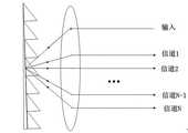
图1为本发明频域线性相移可调光延时系统的结构示意图。FIG. 1 is a schematic structural diagram of a frequency domain linear phase shift adjustable light delay system according to the present invention.
图2为本发明频域线性相移可调光延时系统中光栅型频率分割器结构示意图。FIG. 2 is a structural schematic diagram of a grating type frequency divider in the frequency domain linear phase shift adjustable light delay system of the present invention.
图3为本发明频域线性相移可调光延时系统中薄膜干涉型频率分割器结构示意图。FIG. 3 is a schematic structural diagram of a thin-film interference frequency divider in the frequency-domain linear phase shift adjustable optical delay system of the present invention.
图4为本发明频域线性相移可调光延时系统中光纤布拉格光栅(FBG)型频率分割器结构示意图。Fig. 4 is a structural schematic diagram of a fiber Bragg grating (FBG) type frequency divider in the frequency domain linear phase shift adjustable optical delay system of the present invention.
图5为本发明频域线性相移可调光延时系统中阵列波导光栅(AWG)型频率分割器结构示意图。FIG. 5 is a schematic structural diagram of an arrayed waveguide grating (AWG) type frequency divider in the frequency domain linear phase shift adjustable optical delay system of the present invention.
图6为本发明频域线性相移可调光延时系统中微环级联型频率分割器结构示意图。FIG. 6 is a schematic structural diagram of a microring cascaded frequency divider in the frequency domain linear phase shift adjustable light delay system of the present invention.
图7为双环级联型频率分割器的幅度和相位响应图。Fig. 7 is the magnitude and phase response diagram of the double-loop cascaded frequency divider.
图8为高斯脉冲经过本发明系统后的时域和频域图。Fig. 8 is a time-domain and frequency-domain diagram of a Gaussian pulse passing through the system of the present invention.
图9为高斯脉冲延时图。Figure 9 is a Gaussian pulse delay diagram.
具体实施方式Detailed ways
下面结合附图和实施例对本发明做进一步阐述,但不应以此限制本发明的保护范围。The present invention will be further described below in conjunction with the accompanying drawings and embodiments, but the protection scope of the present invention should not be limited thereby.
图1为本发明频域线性相移可调光延时系统的结构示意图。如图1所示,一种频域线性相移可调光延时系统,包括沿光路依次设置的频率分割器1、线性移相器2和频率合成器3,所述的频率分割器把光信号在频域上等间隔地分割成N个信道信号。多种密集波分复用(DWDM)器件都可以用来实现光信号的频域分割,分别如图2~6所示。图2所示为本发明中频域线性相移可调光延时系统中光栅型频率分割器。图3所示为本发明频域线性相移可调光延时系统中薄膜干涉型频率分割器。图4所示为本发明频域线性相移可调光延时系统中光纤布拉格光栅(FBG)型频率分割器。图5所示为本发明频域线性相移可调光延时系统中阵列波导光栅(AWG)型频率分割器。图6所示为本发明频域线性相移可调光延时系统中微环级联型频率分割器。其中AWG型和微环级联型的频率分割器都便于集成,为本发明的可调延时系统实现单片集成提供可能。图7所示为基于双环级联滤波器型频率分割器的每个信道的幅度响应和相位响应,由图可得此频率分割器能将输入光信号频谱等间隔分割,所需的分割份数N与光信号的带宽和最大延时量有关,光信号的带宽越高、延时越大,所需的频率分割数N越大,否则信号因离散线性相移而引起的畸变将增大。FIG. 1 is a schematic structural diagram of a frequency domain linear phase shift adjustable light delay system according to the present invention. As shown in Figure 1, a frequency-domain linear phase shift adjustable optical delay system includes a
每个信道经过所述的线性移相器进行相位平移,不同信道之间的相移量呈线性关系,线性移相器可以由硅基、石英基和氮化硅基等集成光子器件构成,通过等离子体色散效应或者热光效应来得到连续可调的相位偏移量,频率合成器将所有信道的信号合成为一个信号。Each channel is phase-shifted by the linear phase shifter, and the phase shift between different channels is linear. The linear phase shifter can be composed of silicon-based, quartz-based and silicon nitride-based integrated photonic devices. Through The plasma dispersion effect or thermo-optic effect can be used to obtain continuously adjustable phase offset, and the frequency synthesizer synthesizes the signals of all channels into one signal.
系统中各个器件都可以用集成器件实现,因此本系统最终可以设计成可调光延时集成芯片。假若输入光信号带宽为BW,经过频率分割器后分为N个信道,每个信道带宽为BW/N,分别经过线性移相器,每个信道相位偏移量呈线性关系:第一个信道相位偏移Φ,第二个信道相位偏移2Φ,以此类推,第N个信道相位偏移NΦ,最后N个信道的光信号通过频率合成器合成一个光信号。Each device in the system can be realized by an integrated device, so the system can finally be designed as an integrated chip with adjustable light delay. If the bandwidth of the input optical signal is BW, it is divided into N channels after passing through the frequency divider, and each channel has a bandwidth of BW/N, and passes through the linear phase shifter respectively. The phase shift is Φ, the phase shift of the second channel is 2Φ, and so on, the phase shift of the Nth channel is NΦ, and the optical signals of the last N channels are synthesized into one optical signal by a frequency synthesizer.
图8(a)为输入光信号和输出光信号的时域图,由图可知输出信号相对于输入光信号延时了320ps,输出光能量有所减少,而移相引起的信号展宽对系统的影响不大。通过增加线性移相器的相位偏移量,可以进一步增大延时量。为了避免相位偏移过大造成光信号严重畸变,在增大延时量时需要考虑增加频率分割份数。图8(b)为输入光信号和输出光信号的频域图,由于频率切割并不连续,一部分频率的光能量损耗,使总的输出能量减少。连续调节每个信道线性移相器的相位偏移量,就可以实现光信号延时量的连续可调。如图9所示,调节移相器的相位,使得相位偏移从45°变为180°,输出光信号的延时从240ps变化到320ps,实现了80ps的可调延时量。Figure 8(a) is the time-domain diagram of the input optical signal and the output optical signal. It can be seen from the figure that the output signal is delayed by 320 ps relative to the input optical signal, and the output optical energy is reduced, and the signal broadening caused by phase shift has a great impact on the system. Has little effect. By increasing the phase offset of the linear phase shifter, the amount of delay can be further increased. In order to avoid severe distortion of the optical signal caused by excessive phase offset, it is necessary to consider increasing the number of frequency divisions when increasing the delay amount. Fig. 8(b) is a frequency domain diagram of the input optical signal and the output optical signal. Since the frequency cutting is discontinuous, the optical energy of a part of the frequency is lost, which reduces the total output energy. By continuously adjusting the phase offset of the linear phase shifter of each channel, the continuous adjustment of the optical signal delay can be realized. As shown in Figure 9, the phase of the phase shifter is adjusted so that the phase shift changes from 45° to 180°, and the delay of the output optical signal changes from 240 ps to 320 ps, realizing an adjustable delay of 80 ps.
the
实施例Example
图1中频率分割器和频率合成器都利用基于微环级联的滤波器构成,其结构如图6所示,其中每个信道使用双环级联的方式,可以得到平坦的频率幅度响应,减小滤波损耗。图7所示为上述频率分割器每个信道的频率幅度响应和相位响应,频率分割器的中心波长为1550nm,可将10ps的高斯光脉冲信号的频率等间隔分割成32个信道。线性移相器利用氮化硅波导热光效应来实现线性相位偏移。其中第一个信道移相π,第二个信道移相2π,以此类推,最后一个信道移相32π,最后通过频率合成器,将所有信道的光合成得到了最后的输出光信号。如图8(a)所示,光脉冲信号相对于输入信号延时了320ps,频率分割引入了一定的插入损耗,同时分割32个信道后相位线性平移给信号带来一定的展宽。调节每个信道的相对相位偏移量,可以调节光脉冲信号的延时量。如图9所示,通过调节移相器的偏移相位,使得相位偏移从45°变为180°,输出光信号的延时从240ps变化到320ps,从而实现了80ps延时量的连续可调。Both the frequency divider and the frequency synthesizer in Figure 1 are composed of filters based on micro-ring cascading, and their structure is shown in Figure 6, where each channel uses a double-ring cascading method to obtain a flat frequency-amplitude response, reducing Small filter loss. Figure 7 shows the frequency amplitude response and phase response of each channel of the above frequency divider. The center wavelength of the frequency divider is 1550nm, which can divide the frequency of the 10ps Gaussian optical pulse signal into 32 channels at equal intervals. Linear phase shifters utilize the silicon nitride waveguide thermo-optic effect to achieve linear phase shifting. The first channel is phase-shifted by π, the second channel is phase-shifted by 2π, and so on, and the last channel is phase-shifted by 32π. Finally, the optical signals of all channels are synthesized by a frequency synthesizer to obtain the final output optical signal. As shown in Figure 8(a), the optical pulse signal is delayed by 320 ps relative to the input signal, and the frequency division introduces a certain insertion loss. At the same time, the phase linear translation after dividing 32 channels brings a certain broadening to the signal. By adjusting the relative phase offset of each channel, the delay of the optical pulse signal can be adjusted. As shown in Figure 9, by adjusting the offset phase of the phase shifter, the phase offset changes from 45° to 180°, and the delay of the output optical signal changes from 240 ps to 320 ps, thereby realizing a continuous delay of 80 ps. Tune.
经实验表明,本发明频域线性相移可调光延时系统实现可调光延时。Experiments show that the frequency domain linear phase shift adjustable light delay system of the present invention realizes adjustable light delay.
Claims (8)
Translated fromChinesePriority Applications (1)
| Application Number | Priority Date | Filing Date | Title |
|---|---|---|---|
| CN2012102257891ACN102749782A (en) | 2012-07-03 | 2012-07-03 | Adjustable time delay system of frequency domain linear phase shift |
Applications Claiming Priority (1)
| Application Number | Priority Date | Filing Date | Title |
|---|---|---|---|
| CN2012102257891ACN102749782A (en) | 2012-07-03 | 2012-07-03 | Adjustable time delay system of frequency domain linear phase shift |
Publications (1)
| Publication Number | Publication Date |
|---|---|
| CN102749782Atrue CN102749782A (en) | 2012-10-24 |
Family
ID=47030094
Family Applications (1)
| Application Number | Title | Priority Date | Filing Date |
|---|---|---|---|
| CN2012102257891APendingCN102749782A (en) | 2012-07-03 | 2012-07-03 | Adjustable time delay system of frequency domain linear phase shift |
Country Status (1)
| Country | Link |
|---|---|
| CN (1) | CN102749782A (en) |
Cited By (4)
| Publication number | Priority date | Publication date | Assignee | Title |
|---|---|---|---|---|
| WO2014071631A1 (en)* | 2012-11-12 | 2014-05-15 | 华为技术有限公司 | Wavelength division multiplexing optical network transmission method and apparatus |
| ES2697948A1 (en)* | 2017-07-28 | 2019-01-29 | Univ Valencia Politecnica | TINTAL OPTICAL DELAY LINE AND METHOD FOR TUNING DELAY (Machine-translation by Google Translate, not legally binding) |
| WO2023217153A1 (en)* | 2022-05-09 | 2023-11-16 | 北京万集科技股份有限公司 | Phase shifter |
| US20240061172A1 (en)* | 2021-07-06 | 2024-02-22 | Macom Technology Solutions Holdings, Inc. | Arrayed waveguide gratings with stabilized performance under varying parameters |
Citations (4)
| Publication number | Priority date | Publication date | Assignee | Title |
|---|---|---|---|---|
| JP2001042272A (en)* | 1999-08-03 | 2001-02-16 | Nippon Telegr & Teleph Corp <Ntt> | Polarization dispersion compensation circuit |
| US20010036002A1 (en)* | 1991-04-29 | 2001-11-01 | Guillermo Tearney | Grating based phase control optical delay line |
| JP2003021814A (en)* | 2001-07-09 | 2003-01-24 | Communication Research Laboratory | Optical delay multiplexing circuit |
| US20070122160A1 (en)* | 2005-11-30 | 2007-05-31 | Park Chang-Soo | Phase controllable optical delay interferometer, optical differential phase shift keying demodulator using the same, and demodulating method therefor |
- 2012
- 2012-07-03CNCN2012102257891Apatent/CN102749782A/enactivePending
Patent Citations (4)
| Publication number | Priority date | Publication date | Assignee | Title |
|---|---|---|---|---|
| US20010036002A1 (en)* | 1991-04-29 | 2001-11-01 | Guillermo Tearney | Grating based phase control optical delay line |
| JP2001042272A (en)* | 1999-08-03 | 2001-02-16 | Nippon Telegr & Teleph Corp <Ntt> | Polarization dispersion compensation circuit |
| JP2003021814A (en)* | 2001-07-09 | 2003-01-24 | Communication Research Laboratory | Optical delay multiplexing circuit |
| US20070122160A1 (en)* | 2005-11-30 | 2007-05-31 | Park Chang-Soo | Phase controllable optical delay interferometer, optical differential phase shift keying demodulator using the same, and demodulating method therefor |
Cited By (5)
| Publication number | Priority date | Publication date | Assignee | Title |
|---|---|---|---|---|
| WO2014071631A1 (en)* | 2012-11-12 | 2014-05-15 | 华为技术有限公司 | Wavelength division multiplexing optical network transmission method and apparatus |
| ES2697948A1 (en)* | 2017-07-28 | 2019-01-29 | Univ Valencia Politecnica | TINTAL OPTICAL DELAY LINE AND METHOD FOR TUNING DELAY (Machine-translation by Google Translate, not legally binding) |
| WO2019020860A1 (en)* | 2017-07-28 | 2019-01-31 | Universitat Politècnica De València | Tunable optical delay line and method for tuning the delay |
| US20240061172A1 (en)* | 2021-07-06 | 2024-02-22 | Macom Technology Solutions Holdings, Inc. | Arrayed waveguide gratings with stabilized performance under varying parameters |
| WO2023217153A1 (en)* | 2022-05-09 | 2023-11-16 | 北京万集科技股份有限公司 | Phase shifter |
Similar Documents
| Publication | Publication Date | Title |
|---|---|---|
| JP6387177B2 (en) | Multistage interferometer circuit with waveform shaping function | |
| US9882650B2 (en) | Optical differential signal sending method, apparatus and system | |
| US9829640B2 (en) | Temperature insensitive DEMUX/MUX in silicon photonics | |
| CN103532604B (en) | Based on the Wave-packet shaping network able to programme of light WDM technology | |
| US9325419B1 (en) | Wavelength control of two-channel DEMUX/MUX in silicon photonics | |
| CN109459816B (en) | Silicon-based optical arbitrary waveform generation chip | |
| CN103412367B (en) | On a kind of sheet of integrated light guide chip, polarization does not rely on system | |
| CN108519642B (en) | An integrated optical mode switch compatible with wavelength division multiplexing and mode division multiplexing functions | |
| JP5773521B2 (en) | Mode multiplexer / demultiplexer, optical transceiver, and optical communication system | |
| JP5868341B2 (en) | Optical multiplexer / demultiplexer | |
| Li et al. | The O-band 20-channel 800 GHz Arrayed Waveguide Grating based on silica platform for 1 Tb/s or higher-speed communication system | |
| CN103064199A (en) | Reflection-type adjustable light delay line | |
| CN102749782A (en) | Adjustable time delay system of frequency domain linear phase shift | |
| CN102841406B (en) | Optical staggered filtering device | |
| Yu et al. | Tunable optical delay line for optical time-division multiplexer | |
| CN102043255A (en) | Polarization interference-based full-light OFDM signal multiplexing and demultiplexing device | |
| US20080138014A1 (en) | Wide passband optical interleaver | |
| Narmadhadevi et al. | Performance analysis of different micro ring resonators based on optical delay lines | |
| CN104092497B (en) | A kind of light serioparallel exchange device based on SLALOM | |
| JP2013257354A (en) | Mode multiplexer/demultiplxer, light transmitter/receiver, and optical communication system | |
| Takiguchi | Integrated-optic Demultiplexer for Variable Capacity Optical OFDM Signals Composed of Slab Star Coupler-type Optical DFT Circuit and Variable Optical | |
| Karim | Design of a novel multiplexer/demultiplexer based on polarization beam splitters/combiners and a polarization converter | |
| CN103048809B (en) | Delay adjustable device based on active fiber grating coupler | |
| JP6266315B2 (en) | Wavelength multiplexer / demultiplexer and optical integrated circuit device | |
| Suzuki et al. | WDM tuneable dispersion compensator with PLC ring resonators |
Legal Events
| Date | Code | Title | Description |
|---|---|---|---|
| C06 | Publication | ||
| PB01 | Publication | ||
| C10 | Entry into substantive examination | ||
| SE01 | Entry into force of request for substantive examination | ||
| C02 | Deemed withdrawal of patent application after publication (patent law 2001) | ||
| WD01 | Invention patent application deemed withdrawn after publication | Application publication date:20121024 |