CN102747345A - Method for chemically plating nickel on surface of copper circuit of PCB (printed circuit board) by dipping and activating nickel - Google Patents
Method for chemically plating nickel on surface of copper circuit of PCB (printed circuit board) by dipping and activating nickelDownload PDFInfo
- Publication number
- CN102747345A CN102747345ACN2012102500690ACN201210250069ACN102747345ACN 102747345 ACN102747345 ACN 102747345ACN 2012102500690 ACN2012102500690 ACN 2012102500690ACN 201210250069 ACN201210250069 ACN 201210250069ACN 102747345 ACN102747345 ACN 102747345A
- Authority
- CN
- China
- Prior art keywords
- concentration
- nickel
- activation
- pcb
- solution
- Prior art date
- Legal status (The legal status is an assumption and is not a legal conclusion. Google has not performed a legal analysis and makes no representation as to the accuracy of the status listed.)
- Granted
Links
- PXHVJJICTQNCMI-UHFFFAOYSA-NNickelChemical compound[Ni]PXHVJJICTQNCMI-UHFFFAOYSA-N0.000titleclaimsabstractdescription326
- 229910052759nickelInorganic materials0.000titleclaimsabstractdescription161
- 238000007747platingMethods0.000titleclaimsabstractdescription86
- RYGMFSIKBFXOCR-UHFFFAOYSA-NCopperChemical compound[Cu]RYGMFSIKBFXOCR-UHFFFAOYSA-N0.000titleclaimsabstractdescription67
- 229910052802copperInorganic materials0.000titleclaimsabstractdescription67
- 239000010949copperSubstances0.000titleclaimsabstractdescription67
- 238000000034methodMethods0.000titleclaimsabstractdescription54
- 230000003213activating effectEffects0.000titleclaims2
- 238000007598dipping methodMethods0.000titleabstract2
- 230000004913activationEffects0.000claimsabstractdescription77
- KGBXLFKZBHKPEV-UHFFFAOYSA-Nboric acidChemical compoundOB(O)OKGBXLFKZBHKPEV-UHFFFAOYSA-N0.000claimsabstractdescription14
- 239000004327boric acidSubstances0.000claimsabstractdescription14
- 150000007524organic acidsChemical class0.000claimsabstractdescription14
- 238000002360preparation methodMethods0.000claimsabstractdescription14
- 230000008569processEffects0.000claimsabstractdescription14
- 159000000000sodium saltsChemical class0.000claimsabstractdescription12
- 239000000243solutionSubstances0.000claimsdescription96
- 238000001994activationMethods0.000claimsdescription76
- HEMHJVSKTPXQMS-UHFFFAOYSA-MSodium hydroxideChemical compound[OH-].[Na+]HEMHJVSKTPXQMS-UHFFFAOYSA-M0.000claimsdescription66
- 239000000126substanceSubstances0.000claimsdescription28
- 239000007788liquidSubstances0.000claimsdescription27
- XLYOFNOQVPJJNP-UHFFFAOYSA-NwaterChemical compoundOXLYOFNOQVPJJNP-UHFFFAOYSA-N0.000claimsdescription26
- CDBYLPFSWZWCQE-UHFFFAOYSA-LSodium CarbonateChemical compound[Na+].[Na+].[O-]C([O-])=OCDBYLPFSWZWCQE-UHFFFAOYSA-L0.000claimsdescription20
- 239000000203mixtureSubstances0.000claimsdescription19
- UMGDCJDMYOKAJW-UHFFFAOYSA-NaminothiocarboxamideNatural productsNC(N)=SUMGDCJDMYOKAJW-UHFFFAOYSA-N0.000claimsdescription18
- 239000008367deionised waterSubstances0.000claimsdescription18
- QAOWNCQODCNURD-UHFFFAOYSA-NSulfuric acidChemical compoundOS(O)(=O)=OQAOWNCQODCNURD-UHFFFAOYSA-N0.000claimsdescription17
- JVTAAEKCZFNVCJ-UHFFFAOYSA-Nlactic acidChemical compoundCC(O)C(O)=OJVTAAEKCZFNVCJ-UHFFFAOYSA-N0.000claimsdescription16
- 229910021641deionized waterInorganic materials0.000claimsdescription14
- 235000010338boric acidNutrition0.000claimsdescription13
- KRKNYBCHXYNGOX-UHFFFAOYSA-Ncitric acidChemical compoundOC(=O)CC(O)(C(O)=O)CC(O)=OKRKNYBCHXYNGOX-UHFFFAOYSA-N0.000claimsdescription13
- NTHWMYGWWRZVTN-UHFFFAOYSA-Nsodium silicateChemical compound[Na+].[Na+].[O-][Si]([O-])=ONTHWMYGWWRZVTN-UHFFFAOYSA-N0.000claimsdescription12
- 238000005530etchingMethods0.000claimsdescription11
- 229910000029sodium carbonateInorganic materials0.000claimsdescription10
- 239000001488sodium phosphateSubstances0.000claimsdescription10
- RYFMWSXOAZQYPI-UHFFFAOYSA-Ktrisodium phosphateChemical compound[Na+].[Na+].[Na+].[O-]P([O-])([O-])=ORYFMWSXOAZQYPI-UHFFFAOYSA-K0.000claimsdescription10
- LCPVQAHEFVXVKT-UHFFFAOYSA-N2-(2,4-difluorophenoxy)pyridin-3-amineChemical compoundNC1=CC=CN=C1OC1=CC=C(F)C=C1FLCPVQAHEFVXVKT-UHFFFAOYSA-N0.000claimsdescription9
- CHQMHPLRPQMAMX-UHFFFAOYSA-Lsodium persulfateSubstances[Na+].[Na+].[O-]S(=O)(=O)OOS([O-])(=O)=OCHQMHPLRPQMAMX-UHFFFAOYSA-L0.000claimsdescription9
- 238000003756stirringMethods0.000claimsdescription9
- 239000002253acidSubstances0.000claimsdescription8
- 239000004310lactic acidSubstances0.000claimsdescription8
- 235000014655lactic acidNutrition0.000claimsdescription8
- 150000002815nickelChemical class0.000claimsdescription8
- VMHLLURERBWHNL-UHFFFAOYSA-MSodium acetateChemical compound[Na+].CC([O-])=OVMHLLURERBWHNL-UHFFFAOYSA-M0.000claimsdescription6
- YTAHJIFKAKIKAV-XNMGPUDCSA-N[(1R)-3-morpholin-4-yl-1-phenylpropyl] N-[(3S)-2-oxo-5-phenyl-1,3-dihydro-1,4-benzodiazepin-3-yl]carbamateChemical compoundO=C1[C@H](N=C(C2=C(N1)C=CC=C2)C1=CC=CC=C1)NC(O[C@H](CCN1CCOCC1)C1=CC=CC=C1)=OYTAHJIFKAKIKAV-XNMGPUDCSA-N0.000claimsdescription6
- XBDQKXXYIPTUBI-UHFFFAOYSA-NdimethylselenoniopropionateNatural productsCCC(O)=OXBDQKXXYIPTUBI-UHFFFAOYSA-N0.000claimsdescription6
- JLKDVMWYMMLWTI-UHFFFAOYSA-Mpotassium iodateChemical compound[K+].[O-]I(=O)=OJLKDVMWYMMLWTI-UHFFFAOYSA-M0.000claimsdescription6
- 235000006666potassium iodateNutrition0.000claimsdescription6
- 239000001230potassium iodateSubstances0.000claimsdescription6
- 229940093930potassium iodateDrugs0.000claimsdescription6
- 235000020637scallopNutrition0.000claimsdescription6
- 239000001632sodium acetateSubstances0.000claimsdescription6
- 235000017281sodium acetateNutrition0.000claimsdescription6
- KQJQICVXLJTWQD-UHFFFAOYSA-NN-MethylthioureaChemical compoundCNC(N)=SKQJQICVXLJTWQD-UHFFFAOYSA-N0.000claimsdescription5
- 239000007864aqueous solutionSubstances0.000claimsdescription5
- FGUUSXIOTUKUDN-IBGZPJMESA-NC1(=CC=CC=C1)N1C2=C(NC([C@H](C1)NC=1OC(=NN=1)C1=CC=CC=C1)=O)C=CC=C2Chemical compoundC1(=CC=CC=C1)N1C2=C(NC([C@H](C1)NC=1OC(=NN=1)C1=CC=CC=C1)=O)C=CC=C2FGUUSXIOTUKUDN-IBGZPJMESA-N0.000claimsdescription4
- NWZSZGALRFJKBT-KNIFDHDWSA-N(2s)-2,6-diaminohexanoic acid;(2s)-2-hydroxybutanedioic acidChemical compoundOC(=O)[C@@H](O)CC(O)=O.NCCCC[C@H](N)C(O)=ONWZSZGALRFJKBT-KNIFDHDWSA-N0.000claimsdescription3
- WHUUTDBJXJRKMK-VKHMYHEASA-NL-glutamic acidChemical compoundOC(=O)[C@@H](N)CCC(O)=OWHUUTDBJXJRKMK-VKHMYHEASA-N0.000claimsdescription3
- IKDUDTNKRLTJSI-UHFFFAOYSA-Nhydrazine monohydrateSubstancesO.NNIKDUDTNKRLTJSI-UHFFFAOYSA-N0.000claimsdescription3
- BRWIZMBXBAOCCF-UHFFFAOYSA-NhydrazinecarbothioamideChemical compoundNNC(N)=SBRWIZMBXBAOCCF-UHFFFAOYSA-N0.000claimsdescription3
- 235000019260propionic acidNutrition0.000claimsdescription3
- IUVKMZGDUIUOCP-BTNSXGMBSA-NquinboloneChemical compoundO([C@H]1CC[C@H]2[C@H]3[C@@H]([C@]4(C=CC(=O)C=C4CC3)C)CC[C@@]21C)C1=CCCC1IUVKMZGDUIUOCP-BTNSXGMBSA-N0.000claimsdescription3
- KDYFGRWQOYBRFD-UHFFFAOYSA-NSuccinic acidNatural productsOC(=O)CCC(O)=OKDYFGRWQOYBRFD-UHFFFAOYSA-N0.000claimsdescription2
- KDYFGRWQOYBRFD-NUQCWPJISA-Nbutanedioic acidChemical compoundO[14C](=O)CC[14C](O)=OKDYFGRWQOYBRFD-NUQCWPJISA-N0.000claimsdescription2
- 238000002791soakingMethods0.000claims15
- 238000005303weighingMethods0.000claims5
- 235000019353potassium silicateNutrition0.000claims4
- 238000002203pretreatmentMethods0.000claims4
- 235000017550sodium carbonateNutrition0.000claims4
- 229910000162sodium phosphateInorganic materials0.000claims4
- 241000237509Patinopecten sp.Species0.000claims2
- 239000003795chemical substances by applicationSubstances0.000claims2
- 239000000843powderSubstances0.000claims2
- 230000002829reductive effectEffects0.000claims2
- 229960004249sodium acetateDrugs0.000claims2
- -1vinyl thiocarbamideChemical compound0.000claims2
- 101100136092Drosophila melanogaster peng geneProteins0.000claims1
- QNAYBMKLOCPYGJ-REOHCLBHSA-NL-alanineChemical compoundC[C@H](N)C(O)=OQNAYBMKLOCPYGJ-REOHCLBHSA-N0.000claims1
- 229910000085boraneInorganic materials0.000claims1
- 125000002147dimethylamino groupChemical group[H]C([H])([H])N(*)C([H])([H])[H]0.000claims1
- 229960002989glutamic acidDrugs0.000claims1
- 238000010438heat treatmentMethods0.000claims1
- 238000002156mixingMethods0.000claims1
- 229910052700potassiumInorganic materials0.000claims1
- UORVGPXVDQYIDP-UHFFFAOYSA-NtrihydridoboronSubstancesBUORVGPXVDQYIDP-UHFFFAOYSA-N0.000claims1
- 229920002554vinyl polymerPolymers0.000claims1
- 238000007654immersionMethods0.000abstractdescription42
- KDLHZDBZIXYQEI-UHFFFAOYSA-NPalladiumChemical compound[Pd]KDLHZDBZIXYQEI-UHFFFAOYSA-N0.000abstractdescription32
- 230000003197catalytic effectEffects0.000abstractdescription16
- 229910052763palladiumInorganic materials0.000abstractdescription16
- LGQLOGILCSXPEA-UHFFFAOYSA-Lnickel sulfateChemical compound[Ni+2].[O-]S([O-])(=O)=OLGQLOGILCSXPEA-UHFFFAOYSA-L0.000abstractdescription14
- 229910000363nickel(II) sulfateInorganic materials0.000abstractdescription14
- 238000004519manufacturing processMethods0.000abstractdescription12
- 150000001875compoundsChemical class0.000abstractdescription10
- 239000010970precious metalSubstances0.000abstractdescription5
- 230000008021depositionEffects0.000abstractdescription4
- 230000008859changeEffects0.000abstractdescription3
- 238000009776industrial productionMethods0.000abstractdescription3
- 230000002269spontaneous effectEffects0.000abstractdescription3
- 150000003464sulfur compoundsChemical class0.000abstractdescription3
- 238000012360testing methodMethods0.000description12
- KWSLGOVYXMQPPX-UHFFFAOYSA-N5-[3-(trifluoromethyl)phenyl]-2h-tetrazoleChemical compoundFC(F)(F)C1=CC=CC(C2=NNN=N2)=C1KWSLGOVYXMQPPX-UHFFFAOYSA-N0.000description9
- 238000005238degreasingMethods0.000description9
- 229910001379sodium hypophosphiteInorganic materials0.000description9
- 239000000758substrateSubstances0.000description9
- 239000004115Sodium SilicateSubstances0.000description8
- 239000003638chemical reducing agentSubstances0.000description8
- 229910052911sodium silicateInorganic materials0.000description8
- 229910052717sulfurInorganic materials0.000description8
- BJEPYKJPYRNKOW-REOHCLBHSA-N(S)-malic acidChemical compoundOC(=O)[C@@H](O)CC(O)=OBJEPYKJPYRNKOW-REOHCLBHSA-N0.000description7
- NINIDFKCEFEMDL-UHFFFAOYSA-NSulfurChemical compound[S]NINIDFKCEFEMDL-UHFFFAOYSA-N0.000description7
- BJEPYKJPYRNKOW-UHFFFAOYSA-Nalpha-hydroxysuccinic acidNatural productsOC(=O)C(O)CC(O)=OBJEPYKJPYRNKOW-UHFFFAOYSA-N0.000description7
- 239000001630malic acidSubstances0.000description7
- 235000011090malic acidNutrition0.000description7
- 239000011593sulfurSubstances0.000description7
- RGHNJXZEOKUKBD-SQOUGZDYSA-ND-gluconic acidChemical compoundOC[C@@H](O)[C@@H](O)[C@H](O)[C@@H](O)C(O)=ORGHNJXZEOKUKBD-SQOUGZDYSA-N0.000description6
- XSQUKJJJFZCRTK-UHFFFAOYSA-NUreaNatural productsNC(N)=OXSQUKJJJFZCRTK-UHFFFAOYSA-N0.000description6
- 229910000406trisodium phosphateInorganic materials0.000description6
- 235000019801trisodium phosphateNutrition0.000description6
- PVTGORQEZYKPDK-UHFFFAOYSA-NethenylthioureaChemical compoundNC(=S)NC=CPVTGORQEZYKPDK-UHFFFAOYSA-N0.000description5
- RGHNJXZEOKUKBD-UHFFFAOYSA-ND-gluconic acidNatural productsOCC(O)C(O)C(O)C(O)C(O)=ORGHNJXZEOKUKBD-UHFFFAOYSA-N0.000description4
- 241000237503PectinidaeSpecies0.000description4
- 235000015165citric acidNutrition0.000description4
- 239000000174gluconic acidSubstances0.000description4
- 235000012208gluconic acidNutrition0.000description4
- PCHJSUWPFVWCPO-UHFFFAOYSA-NgoldChemical compound[Au]PCHJSUWPFVWCPO-UHFFFAOYSA-N0.000description4
- 229910052737goldInorganic materials0.000description4
- 239000010931goldSubstances0.000description4
- XUIMIQQOPSSXEZ-UHFFFAOYSA-NSiliconChemical compound[Si]XUIMIQQOPSSXEZ-UHFFFAOYSA-N0.000description3
- 229920000122acrylonitrile butadiene styrenePolymers0.000description3
- 239000011248coating agentSubstances0.000description3
- 238000000576coating methodMethods0.000description3
- 230000008595infiltrationEffects0.000description3
- 238000001764infiltrationMethods0.000description3
- 229910052751metalInorganic materials0.000description3
- 239000002184metalSubstances0.000description3
- 230000003647oxidationEffects0.000description3
- 238000007254oxidation reactionMethods0.000description3
- 229910052710siliconInorganic materials0.000description3
- 239000010703siliconSubstances0.000description3
- DGAQECJNVWCQMB-PUAWFVPOSA-MIlexoside XXIXChemical compoundC[C@@H]1CC[C@@]2(CC[C@@]3(C(=CC[C@H]4[C@]3(CC[C@@H]5[C@@]4(CC[C@@H](C5(C)C)OS(=O)(=O)[O-])C)C)[C@@H]2[C@]1(C)O)C)C(=O)O[C@H]6[C@@H]([C@H]([C@@H]([C@H](O6)CO)O)O)O.[Na+]DGAQECJNVWCQMB-PUAWFVPOSA-M0.000description2
- WNLRTRBMVRJNCN-UHFFFAOYSA-Nadipic acidChemical compoundOC(=O)CCCCC(O)=OWNLRTRBMVRJNCN-UHFFFAOYSA-N0.000description2
- YPTUAQWMBNZZRN-UHFFFAOYSA-NdimethylaminoboronChemical group[B]N(C)CYPTUAQWMBNZZRN-UHFFFAOYSA-N0.000description2
- 238000006073displacement reactionMethods0.000description2
- 230000000694effectsEffects0.000description2
- 239000002245particleSubstances0.000description2
- ACVYVLVWPXVTIT-UHFFFAOYSA-MphosphinateChemical compound[O-][PH2]=OACVYVLVWPXVTIT-UHFFFAOYSA-M0.000description2
- 229910052708sodiumInorganic materials0.000description2
- 239000011734sodiumSubstances0.000description2
- 239000012279sodium borohydrideChemical group0.000description2
- 229910000033sodium borohydrideInorganic materials0.000description2
- 238000005476solderingMethods0.000description2
- 238000005406washingMethods0.000description2
- 229920001661ChitosanPolymers0.000description1
- WHUUTDBJXJRKMK-UHFFFAOYSA-NGlutamic acidNatural productsOC(=O)C(N)CCC(O)=OWHUUTDBJXJRKMK-UHFFFAOYSA-N0.000description1
- VEQPNABPJHWNSG-UHFFFAOYSA-NNickel(2+)Chemical compound[Ni+2]VEQPNABPJHWNSG-UHFFFAOYSA-N0.000description1
- 206010070834SensitisationDiseases0.000description1
- PMZURENOXWZQFD-UHFFFAOYSA-LSodium SulfateChemical compound[Na+].[Na+].[O-]S([O-])(=O)=OPMZURENOXWZQFD-UHFFFAOYSA-L0.000description1
- 239000001361adipic acidSubstances0.000description1
- 235000011037adipic acidNutrition0.000description1
- 235000001014amino acidNutrition0.000description1
- 150000001413amino acidsChemical class0.000description1
- 230000009286beneficial effectEffects0.000description1
- 230000008901benefitEffects0.000description1
- 238000004140cleaningMethods0.000description1
- 230000007797corrosionEffects0.000description1
- 238000005260corrosionMethods0.000description1
- 230000007547defectEffects0.000description1
- 238000011161developmentMethods0.000description1
- 235000013922glutamic acidNutrition0.000description1
- 239000004220glutamic acidSubstances0.000description1
- BHEPBYXIRTUNPN-UHFFFAOYSA-Nhydridophosphorus(.) (triplet)Chemical compound[PH]BHEPBYXIRTUNPN-UHFFFAOYSA-N0.000description1
- 229910001453nickel ionInorganic materials0.000description1
- 229910000510noble metalInorganic materials0.000description1
- 235000005985organic acidsNutrition0.000description1
- 238000012545processingMethods0.000description1
- 238000006722reduction reactionMethods0.000description1
- 238000011160researchMethods0.000description1
- 238000001878scanning electron micrographMethods0.000description1
- 229910052938sodium sulfateInorganic materials0.000description1
- 235000011152sodium sulphateNutrition0.000description1
- 238000010561standard procedureMethods0.000description1
- 235000011149sulphuric acidNutrition0.000description1
- 238000004381surface treatmentMethods0.000description1
- 235000012431wafersNutrition0.000description1
Images


Landscapes
- Chemically Coating (AREA)
- Manufacturing Of Printed Wiring (AREA)
- Electroplating Methods And Accessories (AREA)
Abstract
Translated fromChinese
Description
Translated fromChinese技术领域technical field
本发明属于印刷电路板(PCB)制造领域,涉及一种印刷电路板(PCB)的铜电路表面化学镀镍前的新型无钯活化方法。The invention belongs to the field of printed circuit board (PCB) manufacturing and relates to a novel palladium-free activation method before electroless nickel plating on the copper circuit surface of the printed circuit board (PCB).
背景技术Background technique
印刷电路板(PCB)是通过其绝缘基板上的铜电路来提供电子元件连接的互连件,是现代电子设备的必需部件。然而在PCB的制作过程中,由于铜电路易氧化,导致导电及焊接性能恶化,必须对铜电路进行表面处理以改善铜电路的耐蚀性能和焊接性能。化学镀镍/置换镀金技术是在铜电路表面先化学镀镍再置换镀金,得到的镍/金组合镀层能够有效防止铜电路的氧化并提高可焊性,因此在PCB制造领域被广泛的应用。化学镀镍/置换镀金技术中的化学镀镍是一种可以在具有催化活性的表面自发进行的自催化过程。然而在以次亚磷酸钠为还原剂的化学镀镍液中,铜表面并不能催化次亚磷酸根的氧化,因此无法自发的进行化学镀镍,必须借助活化处理在铜表面引入活性点来诱发化学镀镍的进行。A printed circuit board (PCB) is an interconnect that provides the connection of electronic components through copper circuits on its insulating substrate and is an essential part of modern electronic equipment. However, in the process of PCB manufacturing, since the copper circuit is easily oxidized, the electrical conductivity and soldering performance deteriorate, and the surface treatment of the copper circuit must be carried out to improve the corrosion resistance and soldering performance of the copper circuit. Electroless nickel plating/gold displacement plating technology is to first electroless nickel plating on the surface of copper circuit and then to replace gold plating. The nickel/gold combination coating obtained can effectively prevent the oxidation of copper circuit and improve solderability, so it is widely used in the field of PCB manufacturing. Electroless nickel plating in electroless nickel/gold displacement technology is an autocatalytic process that can occur spontaneously on catalytically active surfaces. However, in the electroless nickel plating solution using sodium hypophosphite as a reducing agent, the copper surface cannot catalyze the oxidation of hypophosphite, so the electroless nickel plating cannot be performed spontaneously, and activation treatment must be used to induce active sites on the copper surface. Electroless nickel plating is performed.
在目前的PCB制造过程中,钯活化是应用最广泛的铜电路表面化学镀镍前的活化方法,其原理就是将铜浸入含有贵金属钯的溶液中获得铜面上的钯活性位,典型的钯活化法包括:敏化-活化法、胶体钯活化法以及离子钯活化法。然而,随着近些年贵金属钯的价格持续飙升,应用于铜电路表面化学镀镍前的钯活化法的成本问题也日益显著,给PCB的生产成本控制带来了巨大的冲击。同时,钯活化液自身的亚稳定性以及所导致的化学镀镍过程中的渗镀现象也进一步增加了PCB的制造成本。因此,开发新型的低成本、高活性、高稳定性而且操作简便的无钯活化法对于PCB制造业来说具有重大意义。In the current PCB manufacturing process, palladium activation is the most widely used activation method before electroless nickel plating on the surface of copper circuits. The principle is to immerse copper in a solution containing precious metal palladium to obtain palladium active sites on the copper surface. Typical palladium Activation methods include: sensitization-activation method, colloidal palladium activation method and ionic palladium activation method. However, as the price of precious metal palladium continues to soar in recent years, the cost problem of the palladium activation method applied before electroless nickel plating on the surface of copper circuits has become increasingly significant, which has brought a huge impact on PCB production cost control. At the same time, the metastability of the palladium activation solution itself and the resulting seepage phenomenon in the electroless nickel plating process further increase the manufacturing cost of the PCB. Therefore, the development of a new palladium-free activation method with low cost, high activity, high stability and easy operation is of great significance to the PCB manufacturing industry.
在这种情况下,许多研究工作已经开始关注对次亚磷酸根氧化同样具有催化活性的金属镍,来代替传统活化方法中采用的贵金属钯。许多特殊基体上化学镀镍的镍活化法已经被报道,比如ABS塑料以及硅片。例如:唐雪娇等采用镍活化法来代替钯活化法成功在ABS塑料上得到了具有催化活性的镍活性点,其原理是在ABS塑料上先化学附着一层壳聚糖膜来固定镍离子,再通过化学还原法得到金属镍催化层;H.F.Hsu和S.Karmalkarz等人分别利用硅在含F-和OH-介质中的不稳定性,实现了两种介质中硅对镍的置换沉积作为化学镀镍活性位的引入方式,达到了无钯活化的目的。然而,应用于铜电路表面化学镀镍前的简单有效的无钯活化法却未见报道。因此,开发针对铜电路表面化学镀镍的操作简便、成本低廉且兼具高活性和化学稳定性的镍活化法对于PCB制造业来说具有非常重要的意义。In this context, many research works have begun to focus on metallic nickel, which is also catalytically active for hypophosphite oxidation, to replace the noble metal palladium used in traditional activation methods. Many nickel activation methods for electroless nickel plating on special substrates have been reported, such as ABS plastics and silicon wafers. For example: Tang Xuejiao et al. used nickel activation instead of palladium activation to successfully obtain catalytically active nickel active sites on ABS plastics. The principle is to chemically attach a layer of chitosan film to fix nickel ions on ABS plastics, and then The metallic nickel catalytic layer was obtained by chemical reduction; HFHsu and S.Karmalkarz et al. took advantage of the instability of silicon in F-and OH- containing media, respectively, and realized the replacement deposition of silicon to nickel in the two media as electroless nickel plating The introduction of the active site achieves the purpose of palladium-free activation. However, a simple and effective palladium-free activation method applied to the surface of copper circuits before electroless nickel plating has not been reported. Therefore, it is of great significance for the PCB manufacturing industry to develop a nickel activation method that is easy to operate, low in cost, and has both high activity and chemical stability for electroless nickel plating on the surface of copper circuits.
发明内容Contents of the invention
本发明是要解决现有的PCB制备过程中铜电路表面化学镀镍必须采用贵金属钯进行活化所导致的活化液稳定性低、易发生渗镀以及PCB制造成本高的技术问题,而提供通过浸镍活化在PCB铜电路表面化学镀镍的方法。The present invention aims to solve the technical problems of low stability of the activation solution, easy occurrence of infiltration and high manufacturing cost of the PCB caused by activation of the electroless nickel plating on the surface of the copper circuit in the existing PCB preparation process. Nickel activation is a method of electroless nickel plating on the surface of PCB copper circuit.
本发明的通过浸镍活化在PCB铜电路表面化学镀镍的方法按照以下步骤进行:The method of electroless nickel plating on PCB copper circuit surface by immersion nickel activation of the present invention is carried out according to the following steps:
一、浸镍液的配制:a、按硼酸的浓度为10~40g/L、有机酸或其钠盐的浓度为0~50g/L、含硫化合物的浓度为30~200g/L、硫酸镍的浓度为5~80g/L分别称取硼酸、有机酸或其钠盐、含硫化合物和硫酸镍;b、将步骤a称取的硼酸溶于去离子水中,然后用硫酸预调整pH值至1.0,得到溶液A;c、将步骤b得到的溶液A加热至50~60℃,然后加入步骤a称取的含硫化合物,搅拌至溶解,得到溶液B;d、将步骤a称取的有机酸或其钠盐加入到溶液B中,并用硫酸或氢氧化钠溶液调整pH值为0.5~1.5,得到溶液C;e、在搅拌的条件下,将步骤a称取的硫酸镍加入到步骤d得到的溶液C中,混合均匀,得到浸镍液;其中步骤一的a中所述的含硫化合物为甲基硫脲、乙烯基硫脲、硫脲、异硫脲和氨基硫脲中的一种或几种的组合;1. Preparation of nickel immersion solution: a. The concentration of boric acid is 10-40g/L, the concentration of organic acid or its sodium salt is 0-50g/L, the concentration of sulfur-containing compounds is 30-200g/L, nickel sulfate The concentration of boric acid, organic acid or its sodium salt, sulfur compound and nickel sulfate is weighed respectively; b, the boric acid weighed in step a is dissolved in deionized water, and then the pH value is pre-adjusted with sulfuric acid to 1.0 to obtain solution A; c. heat solution A obtained in step b to 50-60°C, then add the sulfur-containing compound weighed in step a, stir until dissolved, and obtain solution B; d. Add the acid or its sodium salt into solution B, and adjust the pH value to 0.5 to 1.5 with sulfuric acid or sodium hydroxide solution to obtain solution C; e, under stirring conditions, add the nickel sulfate weighed in step a to step d In the obtained solution C, mix uniformly to obtain a nickel immersion solution; wherein the sulfur-containing compound described in a of step 1 is one of methylthiourea, vinylthiourea, thiourea, isothiourea and thiosemicarbazide one or a combination of several;
二、PCB板前处理:f、按质量百分浓度为98%的H2SO4的浓度为10~50ml/L、过硫酸钠的浓度为20~100g/L的比例,将质量百分浓度为98%的H2SO4和过硫酸钠加入水中,混合均匀,得到微蚀液;g、按氢氧化钠的浓度为5~15g/L、碳酸钠的浓度为20~60g/L、磷酸三钠的浓度为30~50g/L、硅酸钠的浓度为5~10g/L的比例,将氢氧化钠、碳酸钠、磷酸三钠和硅酸钠加入水中,混合均匀,并调节pH值为9.0~13.0,得到化学除油液;h、将印有铜电路的PCB板浸没于温度为20~60℃的化学除油液中,吹入空气搅拌1~10min,然后将PCB板用去离子水清洗;i、将步骤f得到的微蚀液加热至20~40℃,再将经步骤h处理后的PCB板浸没于微蚀液中保持0.5~3.0min,再用去离子水清洗,完成PCB板的前处理;Two, PCB board pretreatment: f, according to the proportion that the concentration of H2 SO4 with a mass percentage concentration of 98% is 10-50ml/L, and the concentration of sodium persulfate is 20-100g/L, the mass percentage concentration is Add 98% H2 SO4 and sodium persulfate into water and mix evenly to obtain a microetching solution; The concentration of sodium is 30-50g/L, and the concentration of sodium silicate is 5-10g/L. Add sodium hydroxide, sodium carbonate, trisodium phosphate and sodium silicate to water, mix well, and adjust the pH value 9.0~13.0, get the chemical degreasing liquid; h, immerse the PCB board printed with the copper circuit in the chemical degreasing liquid with a temperature of 20~60℃, blow in the air and stir for 1~10min, then deionize the PCB board Washing with water; i. Heat the micro-etching solution obtained in step f to 20-40°C, then immerse the PCB board treated in step h in the micro-etching solution for 0.5-3.0min, and then wash it with deionized water to complete Pretreatment of PCB board;
三、浸镍活化及化学镀镍:j、将步骤一得到的浸镍液加热30~70℃,然后将经步骤二完成前处理的PCB板浸没于浸镍液中保持2~60s,取出后用去离子水清洗;k、按NaOH的浓度为4~100g/L、还原剂的浓度为10~50g/L将NaOH和还原剂加入水中,混合均匀,得到激活液;l、按硫酸镍的浓度为20~30g/L、次亚磷酸钠的浓度为23~30g/L、醋酸钠的浓度为5~15g/L、乳酸的浓度为10~20ml/L、干贝素的浓度为5~10g/L、苹果酸的浓度为2~8g/L、碘酸钾的浓度为1~5mg/L的比例配制水溶液,并调节pH值为4.6~5.2,得到化学镀镍液;m、将步骤k制备的激活液加热至40~80℃,然后将经步骤j处理的PCB板浸没于激活液中保持5~60s,取出PCB板,用去离子水清洗后立即浸入温度为80~90℃的步骤l制备的化学镀镍液中进行化学镀镍,完成通过浸镍活化在PCB铜电路表面化学镀镍的过程。3. Nickel immersion activation and electroless nickel plating: j. Heat the nickel immersion solution obtained in step 1 to 30-70°C, then immerse the PCB board that has been pre-treated in
步骤三的k中所述的还原剂为次亚磷酸钠、硼氢化钠、水合肼或者二甲基氨基硼烷;The reducing agent described in step 3 k is sodium hypophosphite, sodium borohydride, hydrazine hydrate or dimethylaminoborane;
本发明印有铜电路的PCB板先经化学除油处理后,再进行微蚀处理,去除铜表面氧化膜,然后浸镍处理,使金属镍沉积在铜表面,得到催化层,再经激活液活化处理,以激发浸镍铜面对于化学镀镍的催化活性,使后续的化学镀镍得以顺利进行。The PCB board printed with the copper circuit of the present invention is first subjected to chemical degreasing treatment, then micro-etching treatment to remove the oxide film on the copper surface, and then nickel immersion treatment to deposit metal nickel on the copper surface to obtain a catalytic layer, and then pass through the activation solution Activation treatment to stimulate the catalytic activity of the nickel-impregnated copper surface for electroless nickel plating, so that the subsequent electroless nickel plating can proceed smoothly.
本发明的浸镍液中添加了含有C=S基团的化合物,可以改变铜和镍之间的电位关系,能够在铜表面实现金属镍的快速自发沉积得到催化层。浸镍过程中镍催化层是通过金属键生长在铜基体上的,镍催化层与基体的结合强度较高,因此生长在镍催化层上的化学镀镍层与基体的结合牢固,不会造成掉镍现象;激活的浸镍层催化活性比较高,可以在化学镀镍的过程中迅速起到活化的效果,化学镀镍启镀速度可以与离子钯活化法相媲美。The compound containing C=S group is added in the nickel immersion solution of the present invention, which can change the potential relationship between copper and nickel, and can realize rapid spontaneous deposition of metallic nickel on the copper surface to obtain a catalytic layer. During the nickel immersion process, the nickel catalytic layer grows on the copper substrate through metal bonds, and the bonding strength between the nickel catalytic layer and the substrate is relatively high, so the electroless nickel plating layer grown on the nickel catalytic layer is firmly bonded to the substrate without causing Nickel drop phenomenon; the activated nickel immersion layer has relatively high catalytic activity, which can quickly activate the electroless nickel plating process, and the electroless nickel plating start-up plating speed can be compared with the ionic palladium activation method.
本发明的方法用的浸镍活化避免了活化过程中贵金属钯的使用,活化液稳定性高且避免了化学镀镍过程中渗镀现象的发生,有效降低了PCB的生产成本;浸镍和激活处理操作都比较简便而且活化速度快、条件温和、效率高,适合大规模PCB工业生产。The immersion nickel activation used in the method of the present invention avoids the use of precious metal palladium in the activation process, the activation solution has high stability and avoids the occurrence of infiltration plating in the electroless nickel plating process, effectively reducing the production cost of PCB; immersion nickel and activation The processing operations are relatively simple and the activation speed is fast, the conditions are mild, and the efficiency is high, which is suitable for large-scale PCB industrial production.
附图说明Description of drawings
图1为试验一经步骤三的m步骤的铜表面浸没于激活液中保持10s之后的扫描电子显微镜照片;Fig. 1 is the scanning electron micrograph after the copper surface of the m step of test one is immersed in the activation solution and keeps for 10s;
图2为试验一经步骤三的m步骤的铜表面浸没于激活液中保持10s之后的EDX谱图;Fig. 2 is the EDX spectrogram after the copper surface of the m step of test one is immersed in the activation solution and kept for 10s;
图3为试验一经步骤三的m步骤的化学镀镍30分钟后的扫描电子显微镜照片;Fig. 3 is the scanning electron microscope photograph after the electroless nickel plating of step 3 m steps of test one after 30 minutes;
图4为试验一经步骤三的m步骤的化学镀镍30分钟后的EDX谱图。Fig. 4 is the EDX spectrogram after 30 minutes of the electroless nickel plating of the step m step of the test one.
具体实施方式Detailed ways
具体实施方式一:本实施方式的通过浸镍活化在PCB铜电路表面化学镀镍的方法按照以下步骤进行:Specific embodiment one: the method for electroless nickel plating on the surface of PCB copper circuit by immersion nickel activation of the present embodiment is carried out according to the following steps:
一、浸镍液的配制:a、按硼酸的浓度为10~40g/L、有机酸或其钠盐的浓度为0~50g/L、含硫化合物的浓度为30~200g/L、硫酸镍的浓度为5~80g/L分别称取硼酸、有机酸或其钠盐、含硫化合物和硫酸镍;b、将步骤a称取的硼酸溶于去离子水中,然后用硫酸预调整pH值至1.0,得到溶液A;c、将步骤b得到的溶液A加热至50~60℃,然后加入步骤a称取的含硫化合物,搅拌至溶解,得到溶液B;d、将步骤a称取的有机酸或其钠盐加入到溶液B中,并用硫酸或氢氧化钠溶液调整pH值为0.5~1.5,得到溶液C;e、在搅拌的条件下,将步骤a称取的硫酸镍加入到步骤d得到的溶液C中,混合均匀,得到浸镍液;其中步骤一的a中所述的含硫化合物为甲基硫脲、乙烯基硫脲、硫脲、异硫脲和氨基硫脲中的一种或几种的组合;1. Preparation of nickel immersion solution: a. The concentration of boric acid is 10-40g/L, the concentration of organic acid or its sodium salt is 0-50g/L, the concentration of sulfur-containing compounds is 30-200g/L, nickel sulfate The concentration of boric acid, organic acid or its sodium salt, sulfur compound and nickel sulfate is weighed respectively; b, the boric acid weighed in step a is dissolved in deionized water, and then the pH value is pre-adjusted with sulfuric acid to 1.0 to obtain solution A; c. heat solution A obtained in step b to 50-60°C, then add the sulfur-containing compound weighed in step a, stir until dissolved, and obtain solution B; d. Add the acid or its sodium salt into solution B, and adjust the pH value to 0.5 to 1.5 with sulfuric acid or sodium hydroxide solution to obtain solution C; e, under stirring conditions, add the nickel sulfate weighed in step a to step d In the obtained solution C, mix uniformly to obtain a nickel immersion solution; wherein the sulfur-containing compound described in a of step 1 is one of methylthiourea, vinylthiourea, thiourea, isothiourea and thiosemicarbazide one or a combination of several;
二、PCB板前处理:f、按质量百分浓度为98%的H2SO4的浓度为10~50ml/L、过硫酸钠的浓度为20~100g/L的比例,将质量百分浓度为98%的H2SO4和过硫酸钠加入水中,混合均匀,得到微蚀液;g、按氢氧化钠的浓度为5~15g/L、碳酸钠的浓度为20~60g/L、磷酸三钠的浓度为30~50g/L、硅酸钠的浓度为5~10g/L的比例,将氢氧化钠、碳酸钠、磷酸三钠和硅酸钠加入水中,混合均匀,并调节pH值为9.0~13.0,得到化学除油液;h、将印有铜电路的PCB板浸没于温度为20~60℃的化学除油液中,吹入空气搅拌1~10min,然后将PCB板用去离子水清洗;i、将步骤f得到的微蚀液加热至20~40℃,再将经步骤h处理后的PCB板浸没于微蚀液中保持0.5~3.0min,再用去离子水清洗,完成PCB板的前处理;Two, PCB board pretreatment: f, according to the proportion that the concentration of H2 SO4 with a mass percentage concentration of 98% is 10-50ml/L, and the concentration of sodium persulfate is 20-100g/L, the mass percentage concentration is Add 98% H2 SO4 and sodium persulfate into water and mix evenly to obtain a microetching solution; The concentration of sodium is 30-50g/L, and the concentration of sodium silicate is 5-10g/L. Add sodium hydroxide, sodium carbonate, trisodium phosphate and sodium silicate to water, mix well, and adjust the pH value 9.0~13.0, get the chemical degreasing liquid; h, immerse the PCB board printed with the copper circuit in the chemical degreasing liquid with a temperature of 20~60℃, blow in the air and stir for 1~10min, then deionize the PCB board Washing with water; i. Heat the micro-etching solution obtained in step f to 20-40°C, then immerse the PCB board treated in step h in the micro-etching solution for 0.5-3.0min, and then wash it with deionized water to complete Pretreatment of PCB board;
三、浸镍活化及化学镀镍:j、将步骤一得到的浸镍液加热30~70℃,然后将经步骤二完成前处理的PCB板浸没于浸镍液中保持2~60s,取出后用去离子水清洗;k、按NaOH的浓度为4~100g/L、次亚磷酸钠的浓度为10~50g/L将NaOH和还原剂加入水中,混合均匀,得到激活液;l、按硫酸镍的浓度为20~30g/L、次亚磷酸钠的浓度为23~30g/L、醋酸钠的浓度为5~15g/L、乳酸的浓度为10~20ml/L、干贝素的浓度为5~10g/L、苹果酸的浓度为2~8g/L、碘酸钾的浓度为1~5mg/L的比例配制水溶液,并调节其pH值为4.6~5.2,得到化学镀镍液;m、将步骤k制备的激活液加热至40~80℃,然后将经步骤j处理的PCB板浸没于激活液中保持5~60s,取出PCB板,用去离子水清洗后立即浸入温度为80~90℃的步骤l制备的化学镀镍液中进行化学镀镍,完成通过浸镍活化在PCB铜电路表面化学镀镍的过程。3. Nickel immersion activation and electroless nickel plating: j. Heat the nickel immersion solution obtained in step 1 to 30-70°C, then immerse the PCB board that has been pre-treated in
本实施方式印有铜电路的PCB板先经化学除油处理后,再进行微蚀处理,去除铜表面氧化膜,然后浸镍处理,使金属镍沉积在铜表面,得到催化层,再经激活液活化处理,以激发浸镍铜面对于化学镀镍的催化活性,使后续的化学镀镍得以顺利进行。本实施方式的浸镍液中添加了含有C=S基团的化合物,可以改变铜和镍之间的电位关系,能够在铜表面实现金属镍的快速自发沉积得到催化层。浸镍过程中镍催化层是通过金属键生长在铜基体上的,镍催化层与基体的结合强度较高,因此生长在镍催化层上的化学镀镍层与基体的结合牢固,不会造成掉镍现象;激活的浸镍层催化活性比较高,可以在化学镀镍的过程中迅速起到活化的效果,化学镀镍启镀速度可以与离子钯活化法相媲美。本实施方式的方法用的浸镍活化避免了活化过程中贵金属钯的使用,活化液稳定性高且避免了化学镀镍过程中渗镀现象的发生,有效降低了PCB的生产成本;浸镍和激活处理操作都比较简便而且活化速度快、条件温和、效率高,适合大规模PCB工业生产。In this embodiment, the PCB printed with a copper circuit is first subjected to chemical degreasing treatment, then micro-etched to remove the oxide film on the copper surface, and then dipped in nickel to deposit metallic nickel on the copper surface to obtain a catalytic layer, and then activated Liquid activation treatment to stimulate the catalytic activity of the nickel-impregnated copper surface for electroless nickel plating, so that the subsequent electroless nickel plating can proceed smoothly. The compound containing C=S group is added to the nickel immersion solution of this embodiment, which can change the potential relationship between copper and nickel, and can realize rapid spontaneous deposition of metallic nickel on the copper surface to obtain a catalytic layer. During the nickel immersion process, the nickel catalytic layer grows on the copper substrate through metal bonds, and the bonding strength between the nickel catalytic layer and the substrate is relatively high, so the electroless nickel plating layer grown on the nickel catalytic layer is firmly bonded to the substrate without causing Nickel drop phenomenon; the activated nickel immersion layer has relatively high catalytic activity, which can quickly activate the electroless nickel plating process, and the electroless nickel plating start-up plating speed can be compared with the ionic palladium activation method. The nickel immersion activation used in the method of this embodiment avoids the use of precious metal palladium in the activation process, and the activation solution has high stability and avoids the occurrence of infiltration plating in the electroless nickel plating process, effectively reducing the production cost of PCB; immersion nickel and The activation treatment operations are relatively simple and the activation speed is fast, the conditions are mild, and the efficiency is high, which is suitable for large-scale PCB industrial production.
具体实施方式二:本实施方式与具体实施方式一不同的是步骤一的a中所述的有机酸为柠檬酸、乳酸、苹果酸、葡萄糖酸、丙酸、己二酸、丁二酸、丙氨酸和谷氨酸中的一种或几种的组合。其它与具体实施方式一相同。Specific embodiment two: the difference between this embodiment and specific embodiment one is that the organic acid described in a of step one is citric acid, lactic acid, malic acid, gluconic acid, propionic acid, adipic acid, succinic acid, propionic acid One or more combinations of amino acid and glutamic acid. Others are the same as in the first embodiment.
本实施方式的有机酸为组合物时,各种有机酸按任意比组合。When the organic acid of this embodiment is a composition, various organic acids are combined in arbitrary ratios.
具体实施方式三:本实施方式与具体实施方式一或二不同的是步骤二的g中所述的化学除油液的配制按氢氧化钠的浓度为10~12g/L、碳酸钠的浓度为30~50g/L、磷酸三钠的浓度为35~40g/L、硅酸钠的浓度为6~8g/L的比例,将氢氧化钠、碳酸钠、磷酸三钠和硅酸钠加入水中,混合均匀,并调节pH值至10.0~13.0。其它与具体实施方式一或二相同。Specific embodiment three: what this embodiment is different from specific embodiment one or two is that the preparation of the chemical degreasing liquid described in the g of
具体实施方式四:本实施方式与具体实施方式一至三之一不同的是步骤三的k中所述的还原剂为次亚磷酸钠、硼氢化钠、水合肼或者二甲基氨基硼烷。其它与具体实施方式一至三之一相同。Embodiment 4: The difference between this embodiment and one of Embodiments 1 to 3 is that the reducing agent described in step 3 k is sodium hypophosphite, sodium borohydride, hydrazine hydrate or dimethylaminoborane. Others are the same as those in the first to third specific embodiments.
具体实施方式五:本实施方式与具体实施方式一至四之一不同的是步骤三的l中所述的化学镀镍液的配制按硫酸镍的浓度为25~27g/L、次亚磷酸钠的浓度为26~29g/L、醋酸钠的浓度为10~12g/L、乳酸的浓度为15~18ml/L、干贝素的浓度为6~8g/L、苹果酸的浓度为3~4g/L、碘酸钾的浓度为2~3mg/L的比例,配制化学镀镍液,并调节pH值至4.8~5.0;其它与具体实施方式一至四之一相同。Specific embodiment five: what this embodiment is different from one of specific embodiments one to four is that the preparation of the electroless nickel plating solution described in 1 of step 3 is that the concentration of nickel sulfate is 25~27g/L, the concentration of sodium hypophosphite The concentration is 26-29g/L, the concentration of sodium acetate is 10-12g/L, the concentration of lactic acid is 15-18ml/L, the concentration of scallops is 6-8g/L, and the concentration of malic acid is 3-4g/L 1. The concentration of potassium iodate is 2-3 mg/L, the electroless nickel plating solution is prepared, and the pH value is adjusted to 4.8-5.0; the others are the same as in one of the specific embodiments 1 to 4.
具体实施方式六:本实施方式与具体实施方式一至五之一不同的是步骤一的a中浸镍液中硼酸的浓度为15~35g/L、有机酸或其钠盐的浓度为5~40g/L、含硫化合物的浓度为50~150g/L、硫酸镍的浓度为10~70g/L。其它与具体实施方式一至五之一相同。Specific embodiment six: the difference between this embodiment and one of specific embodiments one to five is that the concentration of boric acid in the nickel immersion solution in step a is 15-35g/L, and the concentration of organic acid or its sodium salt is 5-40g /L, the concentration of sulfur-containing compounds is 50-150g/L, and the concentration of nickel sulfate is 10-70g/L. Others are the same as one of the specific embodiments 1 to 5.
具体实施方式七:本实施方式与具体实施方式一至六之一不同的是步骤二的f中微蚀液中质量百分浓度为98%的H2SO4的浓度为15~45ml/L、过硫酸钠的浓度为30~80g/L。其它与具体实施方式一至六之一相同。Specific embodiment seven: the difference between this embodiment and one of the specific embodiments one to six is that the concentration ofH2SO4 with a mass percentage concentration of 98% in the microetching solution in step2 is 15-45ml/L. The concentration of sodium sulfate is 30-80g/L. Others are the same as one of the specific embodiments 1 to 6.
具体实施方式八:本实施方式与具体实施方式一至七之一不同的是步骤二的i中微蚀液加热至25~35℃,再将经步骤h处理后的PCB板浸没于微蚀液中保持1.0~2.0min。其它与具体实施方式一至七之一相同。Embodiment 8: The difference between this embodiment and one of Embodiments 1 to 7 is that the microetching solution in step 2 i is heated to 25-35°C, and then the PCB board treated in step h is immersed in the microetching solution Keep it for 1.0-2.0 minutes. Others are the same as one of the specific embodiments 1 to 7.
具体实施方式九:本实施方式与具体实施方式一至八之一不同的是步骤三的j中浸镍液加热至40~60℃,然后将经步骤二完成前处理的PCB板浸没于浸镍液中保持10~50s。其它与具体实施方式一至八之一相同。Embodiment 9: The difference between this embodiment and Embodiments 1 to 8 is that the nickel immersion solution in j of step 3 is heated to 40-60°C, and then the PCB board that has been pretreated in
具体实施方式十:本实施方式与具体实施方式一至九之一不同的是步骤三的m中将激活液加热至50~70℃,然后将经步骤j处理的PCB板浸没于激活液中保持10~50s。其它与具体实施方式一至九之一相同。Embodiment 10: The difference between this embodiment and Embodiment 1 to Embodiment 9 is that in step 3 m, the activation solution is heated to 50-70°C, and then the PCB board treated in step j is immersed in the activation solution for 10 ~50s. Others are the same as one of the specific embodiments 1 to 9.
用以下试验验证本发明的有益效果:Verify beneficial effect of the present invention with following test:
试验一:本发明的通过浸镍活化在PCB铜电路表面化学镀镍的方法按照以下步骤进行:Test one: the method of electroless nickel plating on the surface of PCB copper circuit by immersion nickel activation of the present invention is carried out according to the following steps:
一、浸镍液的配制:a、按硼酸的浓度为25g/L、柠檬酸的浓度为10g/L、苹果酸的浓度为5g/L、葡萄糖酸的浓度为5g/L、甲基硫脲的浓度为30g/L、乙烯基硫脲的浓度为30g/L、硫脲的浓度为40g/L、硫酸镍的浓度为30g/L分别称取硼酸、柠檬酸、苹果酸、葡萄糖酸、甲基硫脲、乙烯基硫脲、硫脲和硫酸镍;b、将步骤a称取的硼酸溶于去离子水中,然后用硫酸预调整pH值至1.0,得到溶液A;c、将步骤b得到的溶液A加热至50~60℃,然后加入步骤a称取的甲基硫脲、乙烯基硫脲和硫脲,搅拌至溶解,得到溶液B;d、将步骤a称取的柠檬酸、苹果酸和葡萄糖酸加入到溶液B中,并用硫酸或氢氧化钠溶液调整pH值为1.0,得到溶液C;e、在搅拌的条件下,将步骤a称取的硫酸镍加入到步骤d得到的溶液C中,混合均匀,得到浸镍液;1. Preparation of nickel immersion solution: a. The concentration of boric acid is 25g/L, the concentration of citric acid is 10g/L, the concentration of malic acid is 5g/L, the concentration of gluconic acid is 5g/L, methylthiourea The concentration of 30g/L, the concentration of vinylthiourea is 30g/L, the concentration of thiourea is 40g/L, and the concentration of nickel sulfate is 30g/L. Weigh boric acid, citric acid, malic acid, gluconic acid, thiourea, vinylthiourea, thiourea and nickel sulfate; b, dissolving the boric acid weighed in step a in deionized water, and then pre-adjusting the pH value to 1.0 with sulfuric acid to obtain solution A; c, obtaining solution A in step b Solution A is heated to 50-60°C, then the methylthiourea, vinylthiourea and thiourea weighed in step a are added, and stirred until dissolved to obtain solution B; d, the citric acid, apple Add acid and gluconic acid into solution B, and adjust the pH value to 1.0 with sulfuric acid or sodium hydroxide solution to obtain solution C; e, under stirring conditions, add the nickel sulfate weighed in step a to the solution obtained in step d In C, mix uniformly to obtain a nickel immersion solution;
二、PCB板前处理:f、按质量百分浓度为98%的H2SO4的浓度为20ml/L、过硫酸钠的浓度为80g/L的比例,将质量百分浓度为98%的H2SO4和过硫酸钠加入水中,混合均匀,得到微蚀液;g、按氢氧化钠的浓度为10g/L、碳酸钠的浓度为50g/L、磷酸三钠的浓度为50g/L、硅酸钠的浓度为10g/L的比例,将氢氧化钠、碳酸钠、磷酸三钠和硅酸钠加入水中,混合均匀,并调节pH值为13.0,得到化学除油液;h、将印有铜电路的PCB板浸没于温度为40℃的化学除油液中,吹入空气搅拌5min,然后将PCB板用去离子水清洗;i、将步骤f得到的微蚀液加热至25℃,再将经步骤h处理后的PCB板浸没于微蚀液中保持1.5min,再用去离子水清洗,完成PCB板的前处理;Two, PCB board pretreatment: f, according to the ratio that the concentration of 98% H2 SO4 is 20ml/L and the concentration of sodium persulfate is 80g/L, the concentration of 98% H2 SOand sodium persulfate are added in water, mixed uniformly to obtain microetching solution; g, the concentration of sodium hydroxide is 10g/L, the concentration of sodium carbonate is 50g/L, and the concentration of trisodium phosphate is 50g/L, The concentration of sodium silicate is the ratio of 10g/L, sodium hydroxide, sodium carbonate, trisodium phosphate and sodium silicate are added into water, mix evenly, and adjust pH value to 13.0, obtain chemical degreasing liquid; h, print Submerge the PCB board with the copper circuit in a chemical degreasing solution at a temperature of 40°C, blow in air and stir for 5 minutes, and then clean the PCB board with deionized water; i. Heat the microetching solution obtained in step f to 25°C, Then immerse the PCB board treated in step h in the microetching solution for 1.5 minutes, and then wash it with deionized water to complete the pretreatment of the PCB board;
三、浸镍活化及化学镀镍:j、将步骤一得到的浸镍液加热60℃,然后将经步骤二完成前处理的PCB板浸没于浸镍液中保持10s,取出后用去离子水清洗;k、按NaOH的浓度为100g/L、次亚磷酸钠的浓度为50g/L将NaOH和还原剂加入水中,混合均匀,得到激活液;l、按硫酸镍的浓度为25g/L、次亚磷酸钠的浓度为27g/L、醋酸钠的浓度为15g/L、乳酸的浓度为12ml/L、干贝素的浓度为5g/L、苹果酸的浓度为4g/L、碘酸钾的浓度为3mg/L的比例配制水溶液,并调节其pH值为5.2,得到化学镀镍液;m、将步骤k制备的激活液加热至60℃,然后将经步骤j处理的PCB板浸没于激活液中保持10s,取出PCB板,用去离子水清洗后立即浸入温度为85℃的步骤l制备的化学镀镍液中进行化学镀镍30分钟,完成通过浸镍活化在PCB铜电路表面化学镀镍的过程。3. Nickel immersion activation and electroless nickel plating: j. Heat the nickel immersion solution obtained in step 1 to 60°C, then immerse the PCB board that has been pretreated in step 2 in the nickel immersion solution for 10 seconds, and use deionized water after taking it out Cleaning; k, the concentration of NaOH is 100g/L, the concentration of sodium hypophosphite is 50g/L NaOH and reducing agent are added in water, mix well, obtain activation solution; l, the concentration of nickel sulfate is 25g/L, The concentration of sodium hypophosphite is 27g/L, the concentration of sodium acetate is 15g/L, the concentration of lactic acid is 12ml/L, the concentration of scallops is 5g/L, the concentration of malic acid is 4g/L, the concentration of potassium iodate Prepare an aqueous solution with a concentration of 3mg/L, and adjust its pH value to 5.2 to obtain an electroless nickel plating solution; m, heat the activation solution prepared in step k to 60°C, and then immerse the PCB board treated in step j in the activation solution Keep in the solution for 10s, take out the PCB board, wash it with deionized water, and immediately immerse it in the electroless nickel plating solution prepared in step 1 at a temperature of 85°C for 30 minutes to complete the electroless nickel plating on the surface of the PCB copper circuit by immersion nickel activation nickel process.
按照《用胶带测试测量附着力的标准方法ASTM D 3359》的方法B(划方格法)测试镀层结合力,在样品表面划相距1mm的纵横各11线形成10×10的方格,然后用胶带粘住样品后迅速揭开,切口边缘完全光滑,没有一个方格出现剥落,达到5B级,说明镀层与基体的结合力优良。According to "Standard Method for Measuring Adhesion with Tape Test ASTM D 3359" method B (square grid method) to test the bonding force of the coating, draw 11 vertical and horizontal lines at a distance of 1mm on the surface of the sample to form a 10×10 grid, and then use After the tape sticks to the sample, it is quickly removed. The edge of the incision is completely smooth, and none of the squares peel off, reaching 5B level, indicating that the bonding force between the coating and the substrate is excellent.
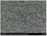
本试验经步骤三的m步骤的铜表面浸没于激活液中保持10s之后的扫描电子显微镜照片如图1所示,从图1可知,经过浸镍活化后黑色的镍颗粒均匀的分布在铜表面,颗粒的大小为0.2~2μm。The scanning electron microscope photo of the copper surface immersed in the activation solution for 10s after the step m of step 3 in this test is shown in Figure 1. From Figure 1, it can be seen that black nickel particles are evenly distributed on the copper surface after nickel immersion activation , The particle size is 0.2-2μm.
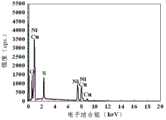
本试验经步骤三的m步骤的铜表面浸没于激活液中保持10s之后的EDX谱图如图2所示,从图2可知,浸镍活化后铜表面的浸镍层的元素组成为Ni和S,其中S元素在浸镍层中的含量为11.6wt%。This test is immersed in the EDX spectrogram after the copper surface of the m step of step 3 is kept in the activation solution for 10s as shown in Figure 2. From Figure 2, it can be known that the elemental composition of the nickel-impregnated layer on the copper surface after nickel-immersion activation is Ni and S, wherein the content of S element in the nickel-immersion layer is 11.6wt%.
本试验经步骤三的m步骤的化学镀镍30分钟后的扫描电子显微镜照片如图3所示,从图3可知,化学镀镍层均匀致密的生长在铜表面,表面没有缺陷。The scanning electron microscope photo of the electroless nickel plating in the m step of step 3 of this test after 30 minutes is shown in Figure 3. From Figure 3, it can be seen that the electroless nickel plating layer grows uniformly and densely on the copper surface without defects on the surface.
本试验经步骤三的m步骤的化学镀镍30分钟后的EDX谱图如图4所示,从图4可知,化学镀镍层的元素组成为Ni和P,其中P元素在化学镀镍层中的含量为10.7wt%,属于高磷化学镀镍层。This test is shown in Figure 4 after the EDX spectrogram of the electroless nickel plating of the m step of step 3 after 30 minutes, as can be seen from Figure 4, the element composition of the electroless nickel plating layer is Ni and P, and wherein P element is in the electroless nickel plating layer The content in is 10.7wt%, which belongs to the high phosphorous electroless nickel plating layer.
Claims (10)
Priority Applications (1)
| Application Number | Priority Date | Filing Date | Title |
|---|---|---|---|
| CN2012102500690ACN102747345B (en) | 2012-07-19 | 2012-07-19 | Method for chemically plating nickel on surface of copper circuit of PCB (printed circuit board) by dipping and activating nickel |
Applications Claiming Priority (1)
| Application Number | Priority Date | Filing Date | Title |
|---|---|---|---|
| CN2012102500690ACN102747345B (en) | 2012-07-19 | 2012-07-19 | Method for chemically plating nickel on surface of copper circuit of PCB (printed circuit board) by dipping and activating nickel |
Publications (2)
| Publication Number | Publication Date |
|---|---|
| CN102747345Atrue CN102747345A (en) | 2012-10-24 |
| CN102747345B CN102747345B (en) | 2013-11-13 |
Family
ID=47027823
Family Applications (1)
| Application Number | Title | Priority Date | Filing Date |
|---|---|---|---|
| CN2012102500690AExpired - Fee RelatedCN102747345B (en) | 2012-07-19 | 2012-07-19 | Method for chemically plating nickel on surface of copper circuit of PCB (printed circuit board) by dipping and activating nickel |
Country Status (1)
| Country | Link |
|---|---|
| CN (1) | CN102747345B (en) |
Cited By (15)
| Publication number | Priority date | Publication date | Assignee | Title |
|---|---|---|---|---|
| CN103484841A (en)* | 2013-10-10 | 2014-01-01 | 青岛黎马敦包装有限公司 | Production technology of fine bronzing plate with high precision and hardness |
| CN103602965A (en)* | 2013-11-18 | 2014-02-26 | 广东哈福科技有限公司 | Chemical nickel plating process for solving problems of diffusion plating and skip plating |
| CN104152879A (en)* | 2014-08-26 | 2014-11-19 | 安捷利电子科技(苏州)有限公司 | A method of manufacturing barrier material-plated copper foil |
| CN104561945A (en)* | 2014-12-31 | 2015-04-29 | 上海安费诺永亿通讯电子有限公司 | LDS electroless plating process |
| CN104862677A (en)* | 2015-05-13 | 2015-08-26 | 电子科技大学 | Method for achieving chemical nickel plating by activating surface of PCB |
| CN104928658B (en)* | 2015-05-13 | 2017-10-17 | 电子科技大学 | A kind of method that activation PCB circuit surfaces realize chemical nickel plating |
| CN107815669A (en)* | 2017-11-02 | 2018-03-20 | 广州市天承化工有限公司 | A kind of method of PCB chemical nickel and golds |
| CN107868947A (en)* | 2017-11-23 | 2018-04-03 | 广东工业大学 | A kind of activating solution and preparation method thereof and no-palladium activating chemical nickel plating method |
| CN108165958A (en)* | 2018-01-25 | 2018-06-15 | 广东工业大学 | A kind of method of red copper surface chemical Ni-P plating-graphene composite deposite |
| CN110257806A (en)* | 2019-06-26 | 2019-09-20 | 捷奈斯科技(深圳)有限公司 | A kind of layering gold plating method for micromotor pcb board |
| CN110724943A (en)* | 2019-11-29 | 2020-01-24 | 四川英创力电子科技股份有限公司 | Palladium-free activating solution before chemical nickel plating on copper surface, preparation method and nickel plating method |
| CN111893464A (en)* | 2020-07-27 | 2020-11-06 | 西安工业大学 | A kind of preparation method of thick Ni-P film plating on the surface of aluminum alloy substrate |
| CN112695320A (en)* | 2020-12-11 | 2021-04-23 | 西安交通大学 | High-flux preparation method of loose ceramic preform |
| CN113151811A (en)* | 2021-04-13 | 2021-07-23 | 赤壁市聚茂新材料科技有限公司 | Non-palladium activated nickel plating solution and nickel plating method |
| CN115015343A (en)* | 2022-06-07 | 2022-09-06 | 中国科学院天津工业生物技术研究所 | A kind of all-solid-state miniature dissolved oxygen electrode fabrication method |
Citations (5)
| Publication number | Priority date | Publication date | Assignee | Title |
|---|---|---|---|---|
| GB802053A (en)* | 1956-05-25 | 1958-09-24 | British Dielectric Res Ltd | Improvements in or relating to the deposition of nickel on dielectric surfaces |
| JPH02111883A (en)* | 1988-10-20 | 1990-04-24 | Toda Kogyo Corp | Electroless metal plating method |
| CN1301881A (en)* | 1999-12-29 | 2001-07-04 | 上海雅驰科技发展有限公司 | Chemical nickel-plating solution and its preparation and using method |
| CN1435509A (en)* | 2002-09-27 | 2003-08-13 | 欧昌亚 | Pre-plating nickel dipping solution for chemical plating aluminium and aluminium alloy with nickel |
| CN101660145A (en)* | 2008-08-28 | 2010-03-03 | 北京玉佳明三态离子科学研究院有限公司 | Formula and technological process of acid plating solution for chemically plating amorphous nickel-phosphorus alloy |
- 2012
- 2012-07-19CNCN2012102500690Apatent/CN102747345B/ennot_activeExpired - Fee Related
Patent Citations (5)
| Publication number | Priority date | Publication date | Assignee | Title |
|---|---|---|---|---|
| GB802053A (en)* | 1956-05-25 | 1958-09-24 | British Dielectric Res Ltd | Improvements in or relating to the deposition of nickel on dielectric surfaces |
| JPH02111883A (en)* | 1988-10-20 | 1990-04-24 | Toda Kogyo Corp | Electroless metal plating method |
| CN1301881A (en)* | 1999-12-29 | 2001-07-04 | 上海雅驰科技发展有限公司 | Chemical nickel-plating solution and its preparation and using method |
| CN1435509A (en)* | 2002-09-27 | 2003-08-13 | 欧昌亚 | Pre-plating nickel dipping solution for chemical plating aluminium and aluminium alloy with nickel |
| CN101660145A (en)* | 2008-08-28 | 2010-03-03 | 北京玉佳明三态离子科学研究院有限公司 | Formula and technological process of acid plating solution for chemically plating amorphous nickel-phosphorus alloy |
Non-Patent Citations (4)
| Title |
|---|
| 《电镀与环保》 20000930 张天顺 等 "TL-3化学镀镍在铜及其合金基体上的镀覆" 第23-25页 1-10 第20卷, 第5期* |
| 《电镀与环保》 20120131 刘海萍 等 "工艺参数对印刷线路板表面化学镀镍/置换镀金层性能的影响" 第15-18页 1-10 第32卷, 第1期* |
| 刘海萍 等: ""工艺参数对印刷线路板表面化学镀镍/置换镀金层性能的影响"", 《电镀与环保》, vol. 32, no. 1, 31 January 2012 (2012-01-31), pages 15 - 18* |
| 张天顺 等: ""TL-3化学镀镍在铜及其合金基体上的镀覆"", 《电镀与环保》, vol. 20, no. 5, 30 September 2000 (2000-09-30), pages 23 - 25* |
Cited By (20)
| Publication number | Priority date | Publication date | Assignee | Title |
|---|---|---|---|---|
| CN103484841B (en)* | 2013-10-10 | 2016-07-20 | 青岛黎马敦包装有限公司 | A kind of production technology of high accuracy and the fine gold stamping version of hardness |
| CN103484841A (en)* | 2013-10-10 | 2014-01-01 | 青岛黎马敦包装有限公司 | Production technology of fine bronzing plate with high precision and hardness |
| CN103602965A (en)* | 2013-11-18 | 2014-02-26 | 广东哈福科技有限公司 | Chemical nickel plating process for solving problems of diffusion plating and skip plating |
| CN104152879A (en)* | 2014-08-26 | 2014-11-19 | 安捷利电子科技(苏州)有限公司 | A method of manufacturing barrier material-plated copper foil |
| CN104561945A (en)* | 2014-12-31 | 2015-04-29 | 上海安费诺永亿通讯电子有限公司 | LDS electroless plating process |
| CN104862677A (en)* | 2015-05-13 | 2015-08-26 | 电子科技大学 | Method for achieving chemical nickel plating by activating surface of PCB |
| CN104862677B (en)* | 2015-05-13 | 2017-08-11 | 电子科技大学 | A kind of method that activation PCB circuit surfaces realize chemical nickel plating |
| CN104928658B (en)* | 2015-05-13 | 2017-10-17 | 电子科技大学 | A kind of method that activation PCB circuit surfaces realize chemical nickel plating |
| CN107815669A (en)* | 2017-11-02 | 2018-03-20 | 广州市天承化工有限公司 | A kind of method of PCB chemical nickel and golds |
| CN107868947B (en)* | 2017-11-23 | 2023-09-19 | 广东工业大学 | Activating solution, preparation method thereof and palladium-free activated chemical nickel plating method |
| CN107868947A (en)* | 2017-11-23 | 2018-04-03 | 广东工业大学 | A kind of activating solution and preparation method thereof and no-palladium activating chemical nickel plating method |
| CN108165958A (en)* | 2018-01-25 | 2018-06-15 | 广东工业大学 | A kind of method of red copper surface chemical Ni-P plating-graphene composite deposite |
| CN110257806A (en)* | 2019-06-26 | 2019-09-20 | 捷奈斯科技(深圳)有限公司 | A kind of layering gold plating method for micromotor pcb board |
| CN110724943A (en)* | 2019-11-29 | 2020-01-24 | 四川英创力电子科技股份有限公司 | Palladium-free activating solution before chemical nickel plating on copper surface, preparation method and nickel plating method |
| CN111893464A (en)* | 2020-07-27 | 2020-11-06 | 西安工业大学 | A kind of preparation method of thick Ni-P film plating on the surface of aluminum alloy substrate |
| CN112695320A (en)* | 2020-12-11 | 2021-04-23 | 西安交通大学 | High-flux preparation method of loose ceramic preform |
| CN112695320B (en)* | 2020-12-11 | 2022-07-12 | 西安交通大学 | A high-throughput preparation method for loosely packed ceramic preforms |
| CN113151811A (en)* | 2021-04-13 | 2021-07-23 | 赤壁市聚茂新材料科技有限公司 | Non-palladium activated nickel plating solution and nickel plating method |
| CN115015343A (en)* | 2022-06-07 | 2022-09-06 | 中国科学院天津工业生物技术研究所 | A kind of all-solid-state miniature dissolved oxygen electrode fabrication method |
| CN115015343B (en)* | 2022-06-07 | 2024-04-26 | 中国科学院天津工业生物技术研究所 | A method for manufacturing an all-solid-state micro dissolved oxygen electrode |
Also Published As
| Publication number | Publication date |
|---|---|
| CN102747345B (en) | 2013-11-13 |
Similar Documents
| Publication | Publication Date | Title |
|---|---|---|
| CN102747345B (en) | Method for chemically plating nickel on surface of copper circuit of PCB (printed circuit board) by dipping and activating nickel | |
| CN110724943A (en) | Palladium-free activating solution before chemical nickel plating on copper surface, preparation method and nickel plating method | |
| CN104862677B (en) | A kind of method that activation PCB circuit surfaces realize chemical nickel plating | |
| CN105018904B (en) | A kind of solution and its plating method for flexible PCB chemical nickel plating | |
| JP2016533430A (en) | Novel adhesion promoter for metallization of substrate surface | |
| TWI876300B (en) | Pre-treatment solution for electroless plating used simultaneously with reduction treatment | |
| TWI687545B (en) | Electroless nickel strike plating solution and method for forming nickel plating film | |
| CN102031505B (en) | Treating fluid for coarsening and activating polyimide and method for coarsening and activating surface of polyimide | |
| CN104928658B (en) | A kind of method that activation PCB circuit surfaces realize chemical nickel plating | |
| CN107868947B (en) | Activating solution, preparation method thereof and palladium-free activated chemical nickel plating method | |
| CN110468394A (en) | A kind of silver-based wiring board of chemical nickel plating porpezite and preparation method thereof | |
| Ogutu et al. | Hybrid method for metallization of glass interposers | |
| CN113005437B (en) | Chemical gold-precipitating liquid for printed circuit board | |
| CN106637159B (en) | A kind of chemical plating solution, preparation method and a kind of non-metal chemical plating method | |
| CN106319485A (en) | Ion palladium activating solution, preparation method and activation method thereof | |
| CN103871540B (en) | A kind of nickel bag glass conductive powder body and preparation method thereof for conductive rubber | |
| CN103572264B (en) | Circuit board surface treatment method | |
| CN103409733A (en) | Metallization method for laser direct structured antenna and chemical copper-precipitated liquid used by the method | |
| KR100759452B1 (en) | Manufacturing method of aluminum nitride substrate with nickel pattern | |
| CN104947110A (en) | Micro etchant, production method of circuit board and circuit board | |
| CN113151812B (en) | A kind of tin activation solution and its preparation method and chemical nickel plating method | |
| CN105112895B (en) | One kind exempts from activation without cyanogen chemical copper plating solution and its copper-plating technique | |
| CN109457239A (en) | The non-cyanogen gold plating liquid of reduced form, gold plating method and gold-plated product | |
| CN114507850A (en) | Chemical formula of an environmentally friendly plating solution for non-formaldehyde electroless copper plating on ceramic substrates by inkjet printing | |
| CN105463416A (en) | Adjusting liquid for chemical roughening of polyimide, and a method for surface chemical roughening of polyimide |
Legal Events
| Date | Code | Title | Description |
|---|---|---|---|
| C06 | Publication | ||
| PB01 | Publication | ||
| C10 | Entry into substantive examination | ||
| SE01 | Entry into force of request for substantive examination | ||
| C14 | Grant of patent or utility model | ||
| GR01 | Patent grant | ||
| CF01 | Termination of patent right due to non-payment of annual fee | Granted publication date:20131113 Termination date:20140719 | |
| EXPY | Termination of patent right or utility model |