CN102741954A - Magnetic circuit for non-contact charging device, power supply device, power receiving device, and non-contact charging device - Google Patents
Magnetic circuit for non-contact charging device, power supply device, power receiving device, and non-contact charging deviceDownload PDFInfo
- Publication number
- CN102741954A CN102741954ACN2011800075089ACN201180007508ACN102741954ACN 102741954 ACN102741954 ACN 102741954ACN 2011800075089 ACN2011800075089 ACN 2011800075089ACN 201180007508 ACN201180007508 ACN 201180007508ACN 102741954 ACN102741954 ACN 102741954A
- Authority
- CN
- China
- Prior art keywords
- magnetic
- coil
- contact charging
- charging device
- coil holder
- Prior art date
- Legal status (The legal status is an assumption and is not a legal conclusion. Google has not performed a legal analysis and makes no representation as to the accuracy of the status listed.)
- Granted
Links
Images


Classifications
- H—ELECTRICITY
- H02—GENERATION; CONVERSION OR DISTRIBUTION OF ELECTRIC POWER
- H02M—APPARATUS FOR CONVERSION BETWEEN AC AND AC, BETWEEN AC AND DC, OR BETWEEN DC AND DC, AND FOR USE WITH MAINS OR SIMILAR POWER SUPPLY SYSTEMS; CONVERSION OF DC OR AC INPUT POWER INTO SURGE OUTPUT POWER; CONTROL OR REGULATION THEREOF
- H02M3/00—Conversion of DC power input into DC power output
- H02M3/22—Conversion of DC power input into DC power output with intermediate conversion into AC
- H02M3/24—Conversion of DC power input into DC power output with intermediate conversion into AC by static converters
- H02M3/28—Conversion of DC power input into DC power output with intermediate conversion into AC by static converters using discharge tubes with control electrode or semiconductor devices with control electrode to produce the intermediate AC
- H02M3/325—Conversion of DC power input into DC power output with intermediate conversion into AC by static converters using discharge tubes with control electrode or semiconductor devices with control electrode to produce the intermediate AC using devices of a triode or a transistor type requiring continuous application of a control signal
- H02M3/335—Conversion of DC power input into DC power output with intermediate conversion into AC by static converters using discharge tubes with control electrode or semiconductor devices with control electrode to produce the intermediate AC using devices of a triode or a transistor type requiring continuous application of a control signal using semiconductor devices only
- H02M3/33538—Conversion of DC power input into DC power output with intermediate conversion into AC by static converters using discharge tubes with control electrode or semiconductor devices with control electrode to produce the intermediate AC using devices of a triode or a transistor type requiring continuous application of a control signal using semiconductor devices only of the forward type
- H02M3/33546—Conversion of DC power input into DC power output with intermediate conversion into AC by static converters using discharge tubes with control electrode or semiconductor devices with control electrode to produce the intermediate AC using devices of a triode or a transistor type requiring continuous application of a control signal using semiconductor devices only of the forward type with automatic control of the output voltage or current
- H02M3/33553—Conversion of DC power input into DC power output with intermediate conversion into AC by static converters using discharge tubes with control electrode or semiconductor devices with control electrode to produce the intermediate AC using devices of a triode or a transistor type requiring continuous application of a control signal using semiconductor devices only of the forward type with automatic control of the output voltage or current with galvanic isolation between input and output of both the power stage and the feedback loop
- H—ELECTRICITY
- H01—ELECTRIC ELEMENTS
- H01F—MAGNETS; INDUCTANCES; TRANSFORMERS; SELECTION OF MATERIALS FOR THEIR MAGNETIC PROPERTIES
- H01F3/00—Cores, Yokes, or armatures
- H01F3/10—Composite arrangements of magnetic circuits
- H—ELECTRICITY
- H01—ELECTRIC ELEMENTS
- H01F—MAGNETS; INDUCTANCES; TRANSFORMERS; SELECTION OF MATERIALS FOR THEIR MAGNETIC PROPERTIES
- H01F38/00—Adaptations of transformers or inductances for specific applications or functions
- H01F38/14—Inductive couplings
- H—ELECTRICITY
- H01—ELECTRIC ELEMENTS
- H01F—MAGNETS; INDUCTANCES; TRANSFORMERS; SELECTION OF MATERIALS FOR THEIR MAGNETIC PROPERTIES
- H01F3/00—Cores, Yokes, or armatures
- H01F3/10—Composite arrangements of magnetic circuits
- H01F2003/103—Magnetic circuits with permanent magnets
Landscapes
- Engineering & Computer Science (AREA)
- Power Engineering (AREA)
- Chemical & Material Sciences (AREA)
- Composite Materials (AREA)
- Charge And Discharge Circuits For Batteries Or The Like (AREA)
Abstract
Description
Translated fromChinese技术领域technical field
本发明涉及电力传送效率几乎不降低而相对于供电装置的一次线圈使受电装置的二次线圈能够可靠地定位的非接触点充电装置、及用于其的磁气回路、供电装置及受电装置。The present invention relates to a non-contact charging device capable of reliably positioning a secondary coil of a power receiving device with respect to a primary coil of a power feeding device without lowering power transmission efficiency, a magnetic circuit used therefor, a power feeding device, and a power receiving device device.
背景技术Background technique
近年来,手机等小型信息通信设备的高性能化及高功能化进展,另外,也要求Web终端及音乐播放器等长时间的连续使用。这些小型信息通信设备或电子设备中,作为电源使用锂离子电池等二次电池。In recent years, high performance and high functionality of small information communication devices such as mobile phones have progressed, and continuous use over a long period of time has also been required for web terminals and music players. In these small information communication devices and electronic devices, secondary batteries such as lithium ion batteries are used as power sources.
二次电池的充电方法有接触充电方式和非接触充电方式。接触充电方式是使受电装置的电极和供电装置的电极直接接触进行充电的方式,构成简单,所以目前被广泛采用,但需要与受电装置的电极形状吻合的连接插头和充电器。非接触充电方式是供电装置及受电装置两方具有线圈且利用电磁感应进行电力传送的方式。非接触充电方式中,不需要用于使供电装置和受电装置直接接触的电极,因此,可以用相同的供电装置对不同的受电装置进行充电。另外,非接触充电方式中,由于不使用可能会腐蚀的电极,所以能够稳定地进行电力的受供电的优点存在。The charging method of the secondary battery includes a contact charging method and a non-contact charging method. The contact charging method is a method in which the electrodes of the power receiving device and the electrodes of the power supply device are directly contacted for charging. It has a simple structure and is currently widely used, but it requires a connecting plug and a charger that match the shape of the electrodes of the power receiving device. The non-contact charging method is a method in which both the power supply device and the power receiving device have coils and use electromagnetic induction to transmit power. In the non-contact charging method, electrodes for directly contacting the power supply device and the power receiving device are not required, so different power receiving devices can be charged by the same power supply device. In addition, in the non-contact charging method, there is an advantage that electric power can be received and fed stably because electrodes that may corrode are not used.
非接触充电装置中,一次线圈中产生的磁通经由供电装置和受电装置的壳体在二次线圈中产生电动势。为提高电力传送效率,在一次线圈及二次线圈的后面设置防止充电中从线圈产生的磁通的泄漏的线圈支架。泄漏磁通流过其它零件或金属部件时,因涡电流而引起发热,但线圈支架作为抑制该发热的磁屏蔽材料起作用。例如特开平11-176677号中公开有在二次线圈和电路零件之间具备铁素体磁芯的非接触充电装置。In the non-contact charging device, the magnetic flux generated in the primary coil generates an electromotive force in the secondary coil via the casings of the power supply device and the power receiving device. In order to improve the power transmission efficiency, a coil holder is installed behind the primary coil and the secondary coil to prevent the leakage of the magnetic flux generated from the coil during charging. When leakage magnetic flux flows through other parts or metal parts, heat is generated by eddy currents, but the coil holder functions as a magnetic shielding material that suppresses this heat. For example, JP-A-11-176677 discloses a non-contact charging device including a ferrite core between a secondary coil and circuit components.
在空芯的一次线圈及二次线圈的情况下,以得到高的电力传送效率的方式尽可能以宽的面积进行重叠,因此,需要使两者的中心轴一致。例如特开平11-176677号中记载有如果两线圈的中心轴错开半径量,则传送电力成为零。为向供电装置可靠地定位受电装置,有将供电装置的壳体与受电装置的壳体嵌合的方式。但是,该方式中,供电装置需要具有与各受电装置相对应的供电面,相对于各种受电装置不能共用供电装置。In the case of air-core primary coils and secondary coils, since they are overlapped over as wide an area as possible to obtain high power transmission efficiency, it is necessary to align the central axes of both. For example, Japanese Unexamined Patent Publication No. 11-176677 discloses that when the central axes of the two coils deviate by a radius, the transmitted power becomes zero. In order to securely position the power receiving device to the power feeding device, there is a method of fitting the case of the power feeding device with the case of the power receiving device. However, in this method, the power feeding device needs to have a power feeding surface corresponding to each power receiving device, and the power feeding device cannot be shared by various power receiving devices.
特开2008-301553号中公开有一种装置,是对手机等被充电设备以非接触式进行充电的装置,在壳体内具备一次线圈的托架具有拥有可以以充裕空间载置被充电设备的面积的大致平板状的载置部,在載置部中与一次线圈的中心相对应的部分设有包含容许范围标记的镜面部,以表示被充电设备的二次线圈的中心位置的中心标记与载置部的容许范围标记相一致的方式将中心标记映射于镜面部,同时将被充电设备定位于载置部上。但是,该装置中,需要在各被充电设备中预先设置中心标记,在设计上不优选,而且使两标记一致的作业在黑暗的地方不能进行的不便存在。Japanese Patent Application Laid-Open No. 2008-301553 discloses a device for non-contact charging of a charged device such as a mobile phone. The bracket equipped with a primary coil in the case has an area capable of placing the charged device with sufficient space. The substantially flat plate-shaped mounting part, in the mounting part corresponding to the center of the primary coil, is provided with a mirror part containing the allowable range mark, so as to indicate the center mark of the center position of the secondary coil of the charged device and the mounting part. The center mark is mapped to the mirror part in a manner consistent with the allowable range mark of the placement part, and the device to be charged is positioned on the placement part at the same time. However, in this device, it is necessary to pre-install the center mark on each charged device, which is not preferable in design, and it is inconvenient that the work of aligning the two marks cannot be performed in a dark place.
特开2009-159677号中公开有一种非接触充电适配器,其在供电装置的供电面及充电装置的充电面的背侧分别安装永久磁铁,且具有用于按照一次线圈和二次线圈的中心轴相一致的方式利用磁气吸附将两者进行定位的安装装置。安装装置由以沿装置的外周环状延伸的方式组合的细的L字型的两个永久磁铁构成。两装置均具有配置于线圈的外侧的环状的永久磁铁,因此,当在线圈的背面设置线圈支架时,从永久磁铁产生的磁通容易流过内侧的线圈支架,接近永久磁铁的线圈支架的部分容易磁饱和。磁饱和的线圈支架部分的磁导率大幅降低,因此,不能充分得到作为磁轭的功能,电力传送效率降低。而且,难以通过稀土类磁铁制作细的L字型的永久磁铁,另外,手操作容易破坏。另外,在利用例如橡胶磁铁制作细的L字型的永久磁铁时,磁力不充分,不能得到足够的定位精度。Japanese Patent Application Laid-Open No. 2009-159677 discloses a non-contact charging adapter, which installs permanent magnets on the back side of the power supply surface of the power supply device and the charging surface of the charging device respectively, and has a central axis for connecting the primary coil and the secondary coil. A mounting device that uses magnetic adsorption to position the two in a consistent manner. The mounting device is composed of two thin L-shaped permanent magnets combined so as to extend annularly along the outer periphery of the device. Both devices have ring-shaped permanent magnets arranged on the outside of the coil. Therefore, when the coil holder is provided on the back of the coil, the magnetic flux generated from the permanent magnet easily flows through the inner coil holder, and the coil holder close to the permanent magnet. Some are prone to magnetic saturation. The magnetic permeability of the magnetically saturated coil holder part is greatly reduced, so that the function as a yoke cannot be sufficiently obtained, and the power transmission efficiency is reduced. Furthermore, it is difficult to produce a thin L-shaped permanent magnet with a rare earth magnet, and it is easily broken by hand. In addition, when a thin L-shaped permanent magnet is manufactured using, for example, a rubber magnet, the magnetic force is insufficient and sufficient positioning accuracy cannot be obtained.
发明内容Contents of the invention
因此,本发明的目的在于,提供几乎不降低电力传送效率而相对于供电装置的一次线圈能够可靠地定位受电装置的二次线圈且具有优异的实用性的非接触充电装置、及用于其的磁气回路、供电装置及受电装置。Therefore, it is an object of the present invention to provide a non-contact charging device that can reliably position the secondary coil of the power receiving device with respect to the primary coil of the power feeding device with little reduction in power transmission efficiency and has excellent practicability, and a non-contact charging device for use therein. The magnetic circuit, power supply device and power receiving device.
本发明的非接触充电装置用磁气回路的特征在于,具备:线圈、配置于所述线圈的后面侧的线圈支架、经由面内方向及/或厚度方向的磁隙配置于所述线圈支架的孔的磁吸附装置。The magnetic circuit for a non-contact charging device according to the present invention is characterized by comprising: a coil, a coil holder arranged on the rear side of the coil, and a coil holder arranged on the coil holder through a magnetic gap in the in-plane direction and/or the thickness direction. Hole magnetic adsorption device.
优选的是,所述线圈支架为具有中央孔的环形板状,所述磁吸附装置同轴配置于所述线圈支架的中央孔内。Preferably, the coil support is in the shape of an annular plate with a central hole, and the magnetic adsorption device is coaxially arranged in the central hole of the coil support.
优选的是,所述磁吸附装置的前面为与所述线圈的前面同高度。即,优选的是,所述磁吸附装置及所述线圈配置于尽可能接近平坦的供电面及充电面。Preferably, the front of the magnetic adsorption device is at the same height as the front of the coil. That is, it is preferable that the magnetic attraction device and the coil are arranged as close as possible to a flat power supply surface and a charge surface.
优选的是,所述磁吸附装置的至少一部分从面内方向观察时,进入所述线圈支架的中央孔。Preferably, at least a part of the magnetic attraction means enters the central hole of the coil holder when viewed from an in-plane direction.
优选的是,所述线圈支架由利用辊急冷法制造的厚度100μm以下的至少一层软磁性合金片构成,所述软磁性合金片的总厚为200μm以下。Preferably, the coil support is composed of at least one layer of soft magnetic alloy sheet with a thickness of 100 μm or less produced by a roller quenching method, and the total thickness of the soft magnetic alloy sheet is 200 μm or less.
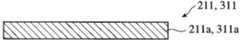
优选的是,所述磁吸附装置由圆板状永久磁铁和具有承受所述圆板状永久磁铁的凹部的具有圆形的帽形状的磁轭部件构成,所述圆板状永久磁铁位于前面侧。Preferably, the magnetic attraction means is composed of a disc-shaped permanent magnet and a circular cap-shaped yoke member having a concave portion for receiving the disc-shaped permanent magnet, and the disc-shaped permanent magnet is located on the front side. .
本发明的非接触充电装置用供电装置的特征在于,具有所述磁气回路。A power supply device for a non-contact charging device according to the present invention includes the magnetic circuit.
本发明的非接触充电装置用受电装置的特征在于,具有所述磁气回路。A power receiving device for a non-contact charging device according to the present invention includes the magnetic circuit.
本发明的非接触充电装置的特征在于,具备具有所述磁气回路的供电装置和具有所述磁气回路的受电装置。A non-contact charging device according to the present invention includes a power supply device having the magnetic circuit and a power receiving device having the magnetic circuit.
本发明的非接触充电装置用磁气回路,磁吸附装置经由磁隙同轴配置于环形板状的线圈支架的中央孔内,因此,为简单的构造,并且能够抑制电力传送效率的降低,并且能够可靠地对供电装置的一次线圈的中心轴定位受电装置的二次线圈的中心轴。另外,本发明的非接触充电装置具有在线圈支架的中央孔的中心配置有小的磁吸附装置的构造,因此,具有优异的实用性,相对于各种受电装置能够由一个供电装置对应。具有这种特征的本发明的非接触充电装置适合手机、便携音乐播放器、便携信息终端、小型计算机、搭载电子电路的手表等小型便携电子制品、或电动牙刷、遥控器等小型电子制品等。In the magnetic circuit for a non-contact charging device according to the present invention, the magnetic attraction device is arranged coaxially in the center hole of the annular plate-shaped coil holder through the magnetic gap, so it has a simple structure and can suppress a decrease in power transmission efficiency, and The center axis of the secondary coil of the power receiving device can be reliably positioned with respect to the center axis of the primary coil of the power feeding device. In addition, the non-contact charging device of the present invention has a structure in which a small magnetic attraction device is arranged in the center of the central hole of the coil holder, and therefore has excellent practicality, and can support various power receiving devices with one power supply device. The non-contact charging device of the present invention having such characteristics is suitable for small portable electronic products such as mobile phones, portable music players, portable information terminals, small computers, and watches equipped with electronic circuits, or small electronic products such as electric toothbrushes and remote controls.
附图说明Description of drawings
图1是表示本发明的非接触充电装置之一例的概略剖面图;1 is a schematic sectional view showing an example of a non-contact charging device of the present invention;
图2是表示图1的非接触充电装置的供电装置的构成的局部剖面平面图;2 is a partial sectional plan view showing the configuration of a power supply device of the non-contact charging device of FIG. 1;
图3是表示用于本发明的非接触充电装置的供电装置之一例的分解立体图;3 is an exploded perspective view showing an example of a power supply device used in the non-contact charging device of the present invention;
图4是表示用于本发明的非接触充电装置的受电装置之一例的分解立体图;4 is an exploded perspective view showing an example of a power receiving device used in the non-contact charging device of the present invention;
图5(a)是表示磁吸附装置和线圈支架的位置关系之一例的局部概略剖面图;Fig. 5 (a) is a partial schematic sectional view showing an example of the positional relationship between the magnetic attraction device and the coil holder;
图5(b)是表示磁吸附装置和线圈支架的位置关系的其它例的局部概略剖面图;Fig. 5 (b) is a partial schematic sectional view showing another example of the positional relationship between the magnetic attraction device and the coil support;
图5(c)是表示磁吸附装置和线圈支架的位置关系的再其它例的局部概略剖面图;Fig. 5 (c) is a partial schematic sectional view showing yet another example of the positional relationship between the magnetic adsorption device and the coil support;
图5(d)是表示磁吸附装置和线圈支架的位置关系的再其它例的局部概略剖面图;Fig. 5 (d) is a partial schematic sectional view showing yet another example of the positional relationship between the magnetic adsorption device and the coil support;
图5(e)是表示磁吸附装置和线圈支架的位置关系的再其它例的局部概略剖面图;Fig. 5 (e) is a partial schematic sectional view showing yet another example of the positional relationship between the magnetic attraction device and the coil support;
图5(f)是表示磁吸附装置和线圈支架的位置关系的再其它例的局部概略剖面图;Fig. 5 (f) is a partial schematic cross-sectional view showing yet another example of the positional relationship between the magnetic adsorption device and the coil support;
图6(a)表示是磁吸附装置之一例的剖面图;Fig. 6 (a) expression is the sectional view of one example of magnetic adsorption device;
图6(b)是表示磁吸附装置的其它例的剖面图;Figure 6 (b) is a cross-sectional view showing another example of the magnetic attraction device;
图6(c)是表示磁吸附装置的再其它例的剖面图;Fig. 6 (c) is a cross-sectional view showing yet another example of the magnetic adsorption device;
图6(d)是表示磁吸附装置的再其它例的剖面图;Fig. 6 (d) is the cross-sectional view showing yet another example of the magnetic adsorption device;
图7是表示本发明的非接触充电装置的其它例的概略剖面图;7 is a schematic sectional view showing another example of the non-contact charging device of the present invention;
图8是表示实施例2中用于磁场解析的非接触充电装置的概略剖面图;8 is a schematic cross-sectional view showing a non-contact charging device used for magnetic field analysis in Example 2;
图9是表示磁吸附装置的外径和线圈支架内的磁通密度的关系的图表;Fig. 9 is a graph showing the relationship between the outer diameter of the magnetic adsorption device and the magnetic flux density in the coil holder;
图10是表示实施例3中用于电力传送效率的测定的非接触充电装置的概略剖面图;10 is a schematic cross-sectional view showing a non-contact charging device used for measurement of power transfer efficiency in Example 3;
图11是图10的局部放大图;Figure 11 is a partial enlarged view of Figure 10;
图12是表示在电力传送效率的测定所使用的电路的框图;Fig. 12 is a block diagram showing a circuit used in the measurement of power transmission efficiency;
图13是表示磁隙和电力传送效率的关系的图表;Fig. 13 is a graph showing the relationship between magnetic gap and power transmission efficiency;
图14是表示距线圈支架的中心的距离和线圈支架内的磁通密度的关系的图表;14 is a graph showing the relationship between the distance from the center of the coil holder and the magnetic flux density in the coil holder;
图15是表示非接触充电装置的电路之一例的框图。FIG. 15 is a block diagram showing an example of a circuit of a non-contact charging device.
具体实施方式Detailed ways
可应用本发明的非接触充电装置,具有图15所示的电路构成。供电装置20具备:供给交流电流的供电部21;为将交流电流整流为直流电流而与供电部21连接的整流电路22;输入直流电流并变换成规定频率的高频电流的开关电路23;以流过高频电流的方式与开关电路23连接的一次线圈201;以在与开关电路23同频率下共振的方式与一次线圈201并联连接的共振用电容器26;与开关电路23连接的控制电路24;与控制电路24连接的控制用一次线圈25。控制电路24基于由控制用一次线圈25得到的感应电流来控制开关电路23的动作。A non-contact charging device to which the present invention can be applied has a circuit configuration as shown in FIG. 15 . The
受电装置30具备:接受从一次线圈201产生的磁通的二次线圈301;与二次线圈301连接的整流电路32;与整流电路32连接的二次电池33;根据二次电池33的电压检测蓄电状态而与二次电池33连接的电池控制电路34;与电池控制电路34连接的控制用二次线圈35。在二次线圈301上也可以并联连接共振用电容器(未图示)。被整流的电流除被蓄电于二次电池33外,还可以用于电子电路或驱动部件(未图示)等。电池控制电路34将用于根据二次电池33的蓄电状态进行最佳的充电的信号流过控制用二次线圈35。例如,在二次电池33为全充电的情况下,使该信息的信号流过控制用二次线圈35,经由与控制用二次线圈35电磁结合的控制用一次线圈25将信号传递给供电装置20的控制电路24。控制电路24基于该信号将开关电路23设为OFF。The
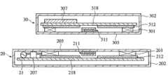
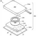
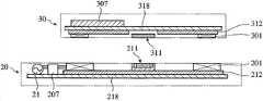
图1~图4表示用于非接触充电装置的供电装置20及受电装置30的构造的优选的一例。非接触充电装置由供电装置20和受电装置30构成,供电装置20具有由一次线圈201、磁吸附装置211及线圈支架212构成的磁气回路,受电装置30具有由二次线圈301、磁吸附装置311及线圈支架312构成的磁气回路。为简便说明,在供电装置20中将一次线圈201、磁吸附装置211及线圈支架212各自的供电面203侧的面称作“前面”,将供电面203的相反侧的面称作“后面”。另外,在受电装置30中将二次线圈301、磁吸附装置311及线圈支架312各自的受电面303侧的面称作“前面”,将受电面303的相反侧的面称作“后面”。另外,将各线圈201、301、磁吸附装置211、311及线圈支架212、312的厚度方向简称为“厚度方向”。1 to 4 show a preferred example of the structure of the
供电装置20的壳体202利用由薄的非磁性树脂板构成的上壳体202a及下壳体202b构成。上壳体202a的上面构成供电面203,背面为平坦。在上壳体202a的平坦的背面中央部固定有:具有平坦的前面的磁吸附装置211、和以使磁吸附装置211经由磁隙得以同轴(同心圆状)地包围的平面螺旋状的且具有平坦的前面的一次线圈201。在此,“同轴”是指磁吸附装置211的中心轴和一次线圈201的中心轴一致,在两者为圆形的情况下,两者为同心圆。一次线圈201按照为了提高与二次线圈301的电磁结合而尽可能接近供电面203的方式配置。磁吸附装置211和一次线圈201的磁隙优选以实质上一次线圈201不受磁吸附装置211的磁通影响的方式增大。通过将一次线圈201设为平面线圈,可以将磁气回路薄型化,可以使供电装置低高度。也可以由绝缘性树脂模制一次线圈201。The
在一次线圈201的后面,同心圆状邻接有大致覆盖一次线圈201的大小的(具有比一次线圈201的外径大的外径和比一次线圈201的内径小的内径)环形板状的线圈支架212,防止由一次线圈201产生的磁通的泄漏。磁吸附装置211从厚度方向观察时,经由磁隙而同心圆状置于线圈支架212的中央孔。因此,磁吸附装置211也可以相对于线圈支架212同心圆状配置。Behind the
在下壳体202b的内面(图3中的上面)固定有基板218。在由电介质构成的基板218上安装有连接一次线圈201的导线端部的线圈端子27、共振用电容器26、整流电路22、开关电路23等。图2中,将共振用电容器26、整流电路22、开关电路23等统一由207表示。A
图4表示在非接触充电装置所使用的受电装置30之一例。受电装置30的壳体302由具有充电时与供电装置20的供电面203相接的充电面303的薄的平坦的树脂板状的下壳体302a、和具有液晶显示部39等的上壳体302b构成。在充电面303的平坦的背侧中央固定有:具有平坦的前面的磁吸附装置311、和以使磁吸附装置311经由磁隙得以同心圆状地包围的平面螺旋状的且具有平坦的前面的二次线圈301。二次线圈301在与一次线圈201对向的位置被配置于充电面303附近。磁吸附装置311和二次线圈301的磁隙,优选以实质上二次线圈301不受磁吸附装置311的磁通影响的方式增大。通过将二次线圈301设为平面线圈,可以将磁气回路薄型化,可以使供电装置低高度。也可以由绝缘性树脂模制二次线圈301。FIG. 4 shows an example of a
在二次线圈301的后面,同心圆状地邻接有大致覆盖二次线圈301的大小的(具有比二次线圈301的外径大的外径和比二次线圈301的内径小的内径)环形板状的线圈支架312,防止由二次线圈301产生的磁通的泄漏。从厚度方向观察时,磁吸附装置311经由磁隙而同心圆状地置于线圈支架312的中央孔。因此,磁吸附装置311也可以相对于线圈支架312同心圆状配置。On the back of the
在上壳体302b的背面(图4中上面)固定有基板318。在由电介质构成的基板318上,除连接二次线圈301的导线端部的线圈端子37、整流电路32及二次电池33外,根据需要还安置有驱动装置(未图示)等。线圈支架312优选以由从二次线圈301产生的磁通不会泄漏的方式与二次线圈301邻接。基板318和线圈支架312也可以不固定。A
在供电装置20及受电装置30的任一磁气回路中,优选磁吸附装置211、311的前面与线圈201、301的前面为相同高度。即,优选磁吸附装置211、311和传送线圈201、301被配置于平坦的供电面203及充电面303附近。配置于前面侧的二次线圈301容易与一次线圈201电磁结合,得到高的电力传送效率。另外,配置于前面侧的磁吸附装置311相对于供电装置20的磁吸附装置311具有大的吸附力,能够以小的永久磁铁容易且正确地进行供电装置20和受电装置30的定位,能够减少从磁吸附装置311泄漏的磁通量。因此,线圈支架312的磁饱和的范围减小,防止线圈支架312的磁导率的降低,得到高的电力传送效率。In any magnetic circuit of the
供电装置20的一次线圈201的卷数也可以比受电装置30的二次线圈301的卷数多。在未如受电装置30那样要求小型化的供电装置20,可使用卷数多的一次线圈201,通过利用相互感应作用而在二次线圈301产生的电压可以在二次电池33中以短时间蓄积电力。磁吸附装置211也可以与受电装置30的磁吸附装置311相同。The number of windings of the
用于线圈支架的软磁性材料优选通过辊急冷制造的厚度100μm以下的Fe系非晶合金、Co系非晶合金、Fe系纳米结晶合金、Co系纳米结晶合金等薄带。例如,在Fe系纳米结晶合金或Co系纳米结晶合金的情况下,优选具有由TaAbMcSidBe(其中,T为Fe及/或Co,A为Cu及/或Au,M为选自Mo、Mn、Cr、Ti、Nb、Ta、W、Al及Sn构成的组中的至少一种元素,a、b、c、d及e以原子%计,分别满足65≤a≤80、0.3≤b≤5、1≤c≤10、5≤d≤15、及5≤e≤15的条件。)表现的基本组成,且平均结晶粒径为50nm以下的微细结晶粒占50体积%以上。A元素在Fe中大致非固溶,是凝集而促进微结晶群的形成的元素。A元素不足0.3原子%时,不能充分发挥其作用,超过5原子%时,容易形成粗大结晶粒,使磁气特性恶化。B及Si是非晶质形成元素。M元素优先进入热处理后残留的非晶相中,因此,辅助Fe浓度高的微细结晶粒的生成,有助于软磁气特性的改善。M元素不足1原子%时,不能充分发挥其作用,超过10原子%时,带来饱和磁通密度的降低。The soft magnetic material used for the coil holder is preferably a thin strip of Fe-based amorphous alloy, Co-based amorphous alloy, Fe-based nanocrystalline alloy, and Co-based nanocrystalline alloy with a thickness of 100 μm or less produced by rapid cooling of a roll. For example, in the case of Fe-based nanocrystalline alloys or Co-based nanocrystalline alloys, it is preferable to have a composition consisting of Ta Ab Mc SidBe (where T is Fe and/or Co, A is Cu and/or Au, M is at least one element selected from the group consisting of Mo, Mn, Cr, Ti, Nb, Ta, W, Al, and Sn, and a, b, c, d, and e are in atomic %, and each satisfies 65≤a ≤80, 0.3≤b≤5, 1≤c≤10, 5≤d≤15, and 5≤e≤15.) The basic composition of the expression, and the average crystal grain size of 50nm or less fine crystal grains accounted for 50 volume % or more. Element A is substantially non-solid-soluble in Fe, and is an element that aggregates to promote the formation of microcrystal groups. When element A is less than 0.3 atomic %, its effect cannot be fully exhibited, and when it exceeds 5 atomic %, coarse crystal grains are likely to be formed, deteriorating the magnetic properties. B and Si are amorphous forming elements. M element preferentially enters the amorphous phase remaining after heat treatment, therefore, assists the formation of fine crystal grains with high Fe concentration, and contributes to the improvement of soft magnetic properties. When the M element is less than 1 atomic %, its effect cannot be fully exhibited, and when it exceeds 10 atomic %, the saturation magnetic flux density decreases.
非接触充电装置以较高的频率进行受供电,当由软磁性金属构成的线圈支架厚时,涡电流损失增大,电力传送效率降低。因此,这些薄带的厚度优选为50μm以下,更优选为30μm以下,特别优选为25μm以下。为抑制涡电流的发生,线圈支架也可以将多个软磁性薄带经由非导电性树脂层层叠而形成。由于供电装置20中不要求薄壁化,所以为降低成本,也可以由具有高饱和磁通密度的铁素体形成线圈支架。The non-contact charging device receives power at a high frequency, and when the coil holder made of soft magnetic metal is thick, the eddy current loss increases and the power transmission efficiency decreases. Therefore, the thickness of these ribbons is preferably 50 μm or less, more preferably 30 μm or less, particularly preferably 25 μm or less. In order to suppress the occurrence of eddy currents, the coil holder may be formed by laminating a plurality of soft magnetic thin strips via non-conductive resin layers. Since thickness reduction is not required in the
非晶合金及纳米结晶合金在低频率带域得到高的磁导率,因此,能够充分抑制泄漏磁通的发生。由纳米结晶合金构成的线圈支架优选在180kHz以下、特别优选在150kHz以下的频率带域使用,由铁素体构成的线圈支架优选在超过180kHz的频率带域使用。Amorphous alloys and nanocrystalline alloys obtain high magnetic permeability in low frequency bands, and therefore can sufficiently suppress the occurrence of leakage magnetic flux. Coil carriers made of nanocrystalline alloys are preferably used in the frequency range below 180 kHz, particularly preferably below 150 kHz, and coil carriers made of ferrite are preferably used in the frequency range above 180 kHz.
线圈支架的总厚(线圈支架内的软磁性片的合计厚度)优选为200m以下,更优选为150μm以下,最为优选为100μm以下,特别优选为50μm以下。例如在手机等便携设备的情况下,通过重叠了两片厚度25μm以下的软磁性片的线圈支架实现本发明的效果。软磁性片越薄,接近线圈支架的磁吸附装置的部分越容易磁饱和,因此,通过在线圈支架和磁吸附装置之间介设磁隙,缩小磁饱和的线圈支架的范围。特别是,由于要求低高度化的非接触充电装置用的磁气回路在厚度方向没有空间上的富裕,所以优选相比厚度方向更在面内方向在线圈支架和磁吸附装置之间形成磁隙。The total thickness of the coil holder (the total thickness of the soft magnetic sheets in the coil holder) is preferably 200 m or less, more preferably 150 μm or less, most preferably 100 μm or less, particularly preferably 50 μm or less. For example, in the case of portable devices such as mobile phones, the effect of the present invention can be achieved by a coil holder in which two soft magnetic sheets with a thickness of 25 μm or less are stacked. The thinner the soft magnetic sheet is, the easier it is to saturate the portion of the magnetic adsorption device close to the coil holder. Therefore, by interposing a magnetic gap between the coil holder and the magnetic adsorption device, the range of the magnetically saturated coil holder is reduced. In particular, since the magnetic circuit for a low-profile non-contact charging device is required to have no space in the thickness direction, it is preferable to form a magnetic gap between the coil holder and the magnetic attraction device in the in-plane direction rather than the thickness direction. .
为防止受电装置及供电装置的落下、冲击等带来的破损,也可以在线圈支架上固定树脂片作为保护片。考虑到受供电时的发热,优选树脂片具有高耐热性。与线圈支架同样地也可以将保护片设为环形板状。In order to prevent the power receiving device and the power supply device from being damaged due to falling, impact, etc., a resin sheet may be fixed on the coil holder as a protective sheet. The resin sheet preferably has high heat resistance in consideration of heat generation when power is supplied. Similarly to the coil holder, the protection sheet may be formed into an annular plate shape.
磁吸附装置211、311和线圈支架212、312之间的各磁隙,也可以是空隙,也可以由磁导率为10以下的材料形成。各磁隙的宽度优选设定为:(a)充分发挥相对于线圈的磁轭功能,并且,(b)防止线圈支架的附近部分的磁饱和并抑制磁导率的降低,以抑制电力传送效率的降低的范围,具体而言,优选设定为0.1~15mm的范围。如果各磁隙的宽度为0.1mm以上,则充分得到线圈支架的磁饱和的抑制效果。各磁隙的宽度优选为0.3mm以上,更优选为0.5mm以上,特别优选为1mm以上。另外,如果各磁隙的宽度为15mm以下,则能够大幅确保线圈支架的面积,因此,能够不使非接触充电装置大型化而得到高的电力传送效率。各磁隙的宽度的上限更优选为10mm,最为优选为8mm。The magnetic gaps between the
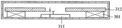
例如在为了提高磁吸附装置211、311的吸附力并使磁吸附装置211、311比线圈201、301厚的情况下,为了使磁气回路低高度化,优选使磁吸附装置211、311的至少一部分在面内方向上位于线圈支架212、312的中央孔的内侧。图5(a)~图5(f)中,以受电装置30为例表示磁吸附装置311和线圈支架312的各种位置关系。任一磁吸附装置311的前面位于与线圈301的前面同一平面上。For example, in order to improve the adsorption force of the
图5(a)表示磁吸附装置311的后面位于与线圈支架312的后面同一平面上的例子。图5(b)表示磁吸附装置311的后面位于比线圈支架312的后面更后方的例子。如图5(a)及图5(b)所示,如果磁吸附装置311位于线圈支架312的中央孔内或向其后方突出,则磁通容易从磁吸附装置311的后面流向线圈支架312的后面侧,线圈支架312的磁饱和的面积减小。图5(c)表示磁吸附装置311的后面位于与线圈支架312的前面同一平面上的例子。FIG. 5( a ) shows an example in which the rear surface of the
图5(d)所示的例子中,从厚度方向观察,磁吸附装置311的至少一部分与线圈支架312重叠,从面内方向观察,两者间有磁隙。为了防止线圈支架312的磁饱和,磁吸附装置311的前面和线圈支架312的后面之间的磁隙T优选为0.1mm以上,更优选为0.2mm以上,最为优选为0.3mm以上。为了受电装置的低高度化,磁隙T的上限优选为1mm,更优选为0.8mm。在线圈支架312的前面侧使用树脂片的情况下,也可以与树脂片分开设置磁隙T。In the example shown in FIG. 5( d ), at least a part of the
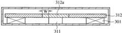
图5(e)所示的例子中,磁吸附装置311由具有中央凸部311c的圆板部d构成,中央凸部311c经由磁隙W置于线圈支架312的中央孔,圆板部d从厚度方向观察经由磁隙T与线圈支架312重叠。优选中央凸部311c为圆形。如果中央凸部311c位于线圈支架312的中央孔内,则磁通容易从凸部311c流入线圈支架312的后面侧,从而线圈支架312的磁饱和的面积减小。In the example shown in Fig. 5 (e), the
图5(f)所示的例子中,线圈支架312的中央孔由树脂片312a覆盖,或者其至少一部分充填有树脂片312a。如果中央孔的磁导率非常低(例如如果为10以下),则能够充分抑制线圈支架312的磁饱和。在由树脂片312a覆盖的情况下,例如在由通过辊急冷制造的软磁性合金薄带构成的线圈支架312上设置的孔的至少一侧粘贴树脂片312a。通过由树脂片312a覆盖中央孔,能够防止金属粉或尘埃等混入磁气回路的内部,另外也能够提高线圈支架312的机械强度。当中央孔的两侧由树脂片312a覆盖时,相对于内部的软磁性金属得到防锈效果。In the example shown in FIG. 5(f), the central hole of the
磁吸附装置311可以是圆形,也可以是正方形等多角形。供电装置30当然也可以使用与上述相同构造的磁气回路。但是,在供电装置20的情况下,磁吸附装置211也可以向比一次线圈201更上方(供电面203侧)错开,例如磁吸附装置211的后面也可以在与一次线圈201的前面同一平面上。The
磁吸附装置211、311优选(a)利用由圆板状永久磁铁211a、311a和软磁性材料构成的磁轭部件211b、311b构成、或(b)仅由圆板状永久磁铁211a、311a构成、或(c)仅由磁轭部件211b、311b构成。图6(a)所示的磁吸附装置211、311由圆板状永久磁铁211a、311a和在前面侧有开口的帽形状的磁轭部件211b、311b构成。磁轭部件211b、311b的开口端优选位于与二次线圈301的前面同一面上。图6(b)所示的磁吸附装置211、311由圆板状永久磁铁211a、311a和圆板状磁轭部件211b、311b构成。图6(c)所示的磁吸附装置211、311仅由圆板状永久磁铁211a、311a构成,图6(d)所示的磁吸附装置211、311仅由圆板状磁轭部件211b、311b构成。在使用图6(d)的磁吸附装置211、311的情况下,供电装置20的磁吸附装置211需要具有永久磁铁3。如果使用圆形的磁吸附装置,则与线圈支架的磁隙均匀,另外受电装置30和供电装置20在任何方向都能够得到一定的吸附力,故而优选。The magnetic attraction means 211, 311 is preferably (a) made of disk-shaped
永久磁铁211a、311a可以使用铁素体磁铁、稀土类磁铁等,但考虑到供电装置20和受电装置30的磁气吸附力、小型化及低高度化,优选NdFeB系稀土类烧结磁铁。作为永久磁铁,即使磁气吸附力比各向同性磁铁强,且供电装置和受电装置在任何方向均接触,也能够产生一定的吸附力,因此,优选在厚度方向配向的各向异性磁铁。如果使用在厚度方向着磁的永久磁铁,则从磁吸附装置的前面出来的磁通量多,但从侧面(与线圈支架的对向面)出来的磁通量少,因此,如果用于图5(a)及图5(b)那样的磁气回路,则能够在抑制线圈支架的磁饱和的同时,发挥大的磁气吸附力。就对稀土类磁铁实施的防氧化用的被覆处理而言,考虑到由线圈201、301产生的磁通对涡电流的影响,优选金属镀敷改为树脂被覆。Ferrite magnets, rare earth magnets, etc. can be used for the
优选在供电装置的一次线圈及受电装置的二次线圈的至少一方,连接有构成共振电路的共振用电容器,更优选在两方连接。特别是在线圈不使用磁芯的非接触充电装置,通过利用共振电路,可以提高电力传送效率。在充电装置具有共振电路的情况下,适宜调整线圈的卷数。A resonant capacitor constituting a resonant circuit is preferably connected to at least one of the primary coil of the power feeding device and the secondary coil of the power receiving device, and more preferably connected to both of them. Especially in a non-contact charging device that does not use a magnetic core for a coil, power transmission efficiency can be improved by using a resonant circuit. When the charging device has a resonant circuit, it is appropriate to adjust the number of turns of the coil.
磁轭部件211b、311b使来自永久磁铁211a、311a的磁通局部集中,提高供电装置20和受电装置30的磁气吸附力,同时,防止来自永久磁铁211a、311a的磁通流入线圈支架212、312。因此,相比磁轭部件211b、311b设为圆板状,如图6(a)所示,优选设为前面侧有开口的圆形的帽状。因此,在使用由永久磁铁211a、311a和磁轭部件211b、311b构成的磁吸附装置211、311的情况下,优选将永久磁铁211a、311a配置于前面侧,将磁轭部件211b、311b配置于后面侧。磁轭部件211b、311b只要是软磁性材料即可,如电磁钢板那样优选为高饱和磁通密度。另外,如果使用磁轭部件211b、311b,则得到相比单独永久磁铁311a的情况可以减薄磁吸附装置的优点。The
优选供电装置20的供电面203和受电装置30的充电面303均平坦,特别优选供电装置30的供电面203平坦。通过平面的供电面203,可以由一个供电装置20对应各种尺寸的受电装置30。Preferably, both the
如果将线圈支架212、312的外径设为比线圈201、301的外径大,则电力传送效率提高,但如果线圈支架212、312的外径过大,则不仅磁气回路大型化,而且电力传送效率饱和。因此,线圈支架212、312的大小根据必要的电力传送效率、及供电装置及受电装置的大小来决定。If the outer diameter of the
图7表示仅受电装置30内的线圈支架312为环形板状且供电装置20内的线圈支架212为平板状的本发明的非接触充电装置的其它例。该例中,供电装置20的线圈支架212可以使用较厚的铁素体板。图7中,将整流电路32、二次电池33、电池控制电路34等汇总用307表示。另外,也可以将磁吸附装置211设为图6(a)~图6(c)所示的使用永久磁铁211a的构造,将磁吸附装置311设为图6(d)所示的磁轭部件311b单独的构造。由于薄型化的要求在受电装置30一方强,所以也可以由薄的磁轭部件311b单独构成磁吸附装置311。另外,如果内装有复杂的电路的受电装置30使用仅由磁轭部件311b构成的磁吸附装置,则设计电路的稳定动作。另外,如果在受电装置30上设置仅由非晶合金或纳米结晶合金构成的线圈支架312且供电装置20使用廉价的铁素体板,则在成本降低方面有效。7 shows another example of the non-contact charging device of the present invention in which only the
通过以下的实施例更详细说明本发明,但本发明不限于此。The present invention will be described in detail through the following examples, but the present invention is not limited thereto.
实施例1Example 1
通过图1所示的构造制作具有下述尺寸的非接触充电装置,且进行磁场解析。With the structure shown in FIG. 1 , a non-contact charging device having the following dimensions was produced, and magnetic field analysis was performed.
(1)供电装置(1) Power supply device
将一次线圈201和环形板状的线圈支架212同心圆状粘接,在线圈支架212的中央孔同心圆状配置图6(a)所示的磁吸附装置211,由此制作图1所示的供电装置20。一次线圈201由卷数20匝且线径0.5mm的铜线构成,为内径15mm、外径35mm及厚度1mm。环形板状的线圈支架212为内径10mm及外径40mm、且使两片厚度20μm的Fe基纳米结晶合金薄带(日立金属株式会社制的“フアインメツトFT1”)层叠、并在其两面层叠厚度50μm的聚对苯二甲酸乙二醇酯(PET)薄膜而形成。磁吸附装置211由外径8mm、内径7mm、壁厚0.5mm及凹部的深度0.5mm的帽形状的磁轭部件211b;固定于磁轭部件211b的凹部的内径6mm及外径7mm的磁隙形成用非磁性环;固定于非磁性环的内侧的直径6mm及厚度0.5mm的圆板状永久磁铁211a所构成。永久磁铁211a由树脂被覆的NdFeB系稀土类磁铁(日立金属株式会社制的“NEOMAX(NMX-S36UH)”、Br=1.2T)构成。磁吸附装置211的前面和一次线圈201的前面为相同高度。The
(2)受电装置(2) Power receiving device
将二次线圈301和环形板状的线圈支架312同心圆状粘接,在线圈支架312的中央孔同心圆状地配置图6(a)所示的磁吸附装置311,由此制作图1所示的受电装置30。二次线圈301由卷数10匝且线径0.5mm的铜线构成,为内径20mm、外径30mm及厚度1mm。环形板状线圈支架312为内径10mm及外径35mm、且使两片厚度20μm的Fe基纳米结晶合金薄带(日立金属株式会社制的“フアインメツトFT1”)层叠、并在其两面层叠厚度50μm的PET薄膜而形成。磁吸附装置311为与磁吸附装置211相同的构成。磁吸附装置311的前面和二次线圈301的前面为相同高度。The
(3)磁场解析结果(3) Magnetic field analysis results
将供电装置20及受电装置30的接触面侧的壳体的厚度分别设为0.5mm,将两磁吸附装置211、311间的距离设为1mm,进行磁场解析,其结果是,磁吸附装置211、311间的吸附力为1.1N,受电装置30的线圈支架312内的最大磁通密度为0.4T。The thickness of the case on the contact surface side of the
实施例2Example 2
图8所示的非接触充电装置中,通过磁场解析求出磁吸附装置311的外径和线圈支架312内的磁通密度的关系。一次线圈201由卷数16匝且线径0.5mm的铜线构成,为内径17mm、外径36mm及厚度1.0mm,二次线圈301由卷数8匝且线径0.5mm的铜线构成,为内径22mm、外径32mm及厚度0.5mm。内径10mm及外径40mm及厚度1.0mm的环形板状线圈支架212由Mn-Zn系铁素体形成。内径10mm及外径35mm的环形板状线圈支架312通过经由厚度10μm的粘接带层叠两片厚度20μm的Fe基纳米结晶合金薄带(日立金属株式会社制的“フアインメツトFT1”)而形成。将磁吸附装置211的前面设为与线圈201的前面相同高度,将磁吸附装置311的前面也设为与线圈301的前面相同高度。磁吸附装置211、311均为表1所示的尺寸且具有图6(a)所示的形状。将磁吸附装置211的后面设为与线圈支架212的前面相同高度,将磁吸附装置311的厚度方向中心设为与线圈支架312的厚度方向中心相同高度。图9表示以在20℃下输入频率120kHz的电流的条件进行磁场解析的结果。In the non-contact charging device shown in FIG. 8 , the relationship between the outer diameter of the
表1]Table 1]

磁轭部件的外径与线圈支架312的中央孔的直径相同,且在磁吸附装置和线圈支架312之间没有磁隙的试样1中,接近磁吸附装置的线圈支架312的部分饱和(达到与Fe基纳米结晶合金的饱和磁通密度相同的约1.2T),另外,即使施加磁通,也不能起到作为磁轭的作用,从而非接触充电装置的电力传送效率降低。The outer diameter of the yoke part is the same as the diameter of the central hole of the
与之相对,在磁吸附装置和线圈支架312的中央孔内面之间介设磁隙的试样2~6中,成为比试样1低的磁通密度,抑制了线圈支架312的磁饱和。磁隙越大,线圈支架312内的磁通密度越低。通过抑制线圈支架的磁导率降低,非接触充电装置的电力传送效率提高。线圈支架内的磁通密度通过磁隙、磁吸附装置的永久磁铁等发生变动,因此,需要将这些尺寸最佳化。In contrast, in
实施例3Example 3
图10所示的非接触充电装置中,求出磁吸附装置和线圈支架之间的磁隙的宽度和非接触充电装置的电力传送效率的关系。In the non-contact charging device shown in FIG. 10 , the relationship between the width of the magnetic gap between the magnetic attraction device and the coil holder and the power transmission efficiency of the non-contact charging device was obtained.
(1)供电装置(1) Power supply device
将外径40mm及厚度1mm的由铁素体圆板构成的线圈支架212固定于树脂制的基板218上。在线圈支架212上,作为一次线圈201同心圆状地重叠卷数16匝且由线径0.5mm的铜线构成且被覆了外径40mm、内径20mm及厚度0.5mm的树脂的平面线圈。作为磁吸附装置211,将外径15mm、厚度1.5mm及厚度0.5mm的圆板状永久磁铁(表面磁通密度=150mT)与一次线圈201同心圆状地配置。将磁吸附装置211的前面和线圈201的前面设为同高度。A
(2)受电装置(2) Power receiving device
环形板状线圈支架312通过将厚度18μm的Fe基纳米结晶合金薄带(日立金属株式会社制的“フアインメツトFT3”)经由厚度10μm的粘接片分别层叠三层、六层、九层而形成。线圈支架312固定于厚度3mm的铝合金基板318上。表2表示各层数的线圈支架312的外径及内径。The annular plate-shaped
表2]Table 2]

作为二次线圈301,使用卷数8匝且由线径0.5mm的铜线构成且被覆了外径40mm、内径20mm及厚度0.5mm的树脂的平面线圈。作为磁吸附装置311,与线圈支架312同心圆状地配置直径15mm及厚度0.5mm的软磁性冷轧钢圆板。将磁吸附装置311的前面以与二次线圈301的前面同高度的方式固定于树脂板11上。图11中放大表示受电装置30的磁吸附装置311的外周面和线圈支架312的中央孔的内周面之间的磁隙W。As the
(3)电力传送效率的测定(3) Measurement of power transmission efficiency
使一次线圈201和二次线圈301经由厚度1.5mm的树脂板11同轴对向,如图12所示与测定器连接。调整共振用电容器26的电容,使一次线圈201和二次线圈301可共振。向供电装置20的一次线圈201在20℃下输入频率120kHz的电流,通过下式求出电力传送效率。结果示于图13。The
电力传送效率P=(V2×A2)/(V1×A1)Power transmission efficiency P=(V2×A2)/(V1×A1)
(其中,V1是一次线圈201和共振用电容器26的串联共振电路的两端间的电压值,A1是流过一次线圈201的电流值,V2是二次线圈301的两端间的电压值,A2是流过二次线圈301的电流值。)(Where, V1 is the voltage value between the two ends of the series resonance circuit of the
自图13表明,电力传送效率在比0mm大的磁隙W下为极大。伴随线圈支架312的中央孔的直径增大且磁隙W增大,线圈支架312的面积减小,因此,预想到电力传送效率降低,但通过在磁吸附装置311和线圈支架312之间设置磁隙,可知电力传送效率反而提高。该趋势在使用图6(a)、图6(b)及图6(c)所示的磁吸附装置的情况下也能够看到。It is clear from FIG. 13 that the power transmission efficiency is maximum at a magnetic gap W larger than 0 mm. As the diameter of the central hole of the
任一线圈支架312均是Fe基纳米结晶合金薄带的总厚越大则电力传送效率P越大。具体而言,在9层线圈支架312(Fe基纳米结晶合金薄带的总厚为150μm以上)的情况下,磁隙W为2.5mm及5mm时的电力传送效率P比磁隙W为0mm时的电力传送效率P大8%以上。在6层线圈支架312(Fe基纳米结晶合金薄带的总厚为100μm以上)的情况下,磁隙W为5mm时的电力传送效率P比磁隙W为0mm时的电力传送效率P大10%以上。在3层线圈支架312(Fe基纳米结晶合金薄带的总厚为50μm以上)的情况下,磁隙W为2.5mm、5mm及7.5mm时的电力传送效率P比磁隙W为0mm时的电力传送效率P大10%以上。特别是,磁隙W为7.5mm时的电力传送效率P比磁隙W为0mm时的电力传送效率P大20%以上。Any
实施例4Example 4
对于图8所示的非接触充电装置的供电装置20及受电装置30有定位用的磁吸附装置211、311和没有定位用磁吸附装置211、311的情况,通过磁场解析求电力传送效率。作为磁吸附装置211、311,使用表1所示的试样2。向供电装置20的一次线圈201在20℃下输入频率120kHz的电流,根据使用图12所示的测定器得到的V1、V2、A1及A2,利用与实施例3相同的式求出电力传送效率。For the cases where the
没有磁吸附装置的情况下的电力传送效率为89.0%,与之相对,有磁吸附装置的情况下的电力传送效率为88.6%。用于磁吸附装置的永久磁铁及金属制磁轭部件成为电力传送效率降低的原因,但由于经由磁隙与线圈支架及线圈进行配置,所以可知其影响极小。The power transmission efficiency without the magnetic adsorption device was 89.0%, whereas the power transmission efficiency with the magnetic adsorption device was 88.6%. The permanent magnets and metal yoke members used in the magnetic attraction device cause a reduction in power transmission efficiency, but since they are arranged with the coil holder and the coil through the magnetic gap, it can be seen that the influence is minimal.
实施例5Example 5
图8所示的构造的供电装置20及受电装置30中,使用具有10mm的外径的图6(b)所示的磁吸附装置211、311、和具有6mm的外径的图6(c)所示的磁吸附装置211、311,通过磁场解析求出距受电装置30的线圈支架312的中央孔(半径5mm)中心的距离和线圈支架312内的磁通密度的关系。图14表示结果。In the
在各磁吸附装置的外径为10mm的情况下,各磁吸附装置和线圈支架接触,因此,线圈支架局部磁饱和。另一方面,在各磁吸附装置的外径为6mm的情况下,在线圈支架和磁吸附装置之间有2mm的磁气间隙,因此,线圈支架未饱和。另外,由永久磁铁和磁轭部件构成的图6(a)所示的磁吸附装置一方相比由永久磁铁单体构成的图6(c)所示的磁吸附装置,线圈支架内部的磁通密度大,但磁气吸附力高。通过减小永久磁铁,可以降低线圈支架内的磁通密度。When the outer diameter of each magnetic attraction device is 10 mm, each magnetic attraction device is in contact with the coil holder, and therefore, the coil holder is partially magnetically saturated. On the other hand, when the outer diameter of each magnetic attraction device is 6 mm, there is a magnetic air gap of 2 mm between the coil holder and the magnetic attraction device, and therefore, the coil holder is not saturated. In addition, the magnetic attraction device shown in FIG. 6(a) composed of permanent magnets and yoke components is compared with the magnetic attraction device shown in FIG. 6(c) composed of permanent magnets alone, and the magnetic flux inside the coil holder High density, but high magnetic adsorption force. By reducing the size of the permanent magnets, the magnetic flux density in the coil holder can be reduced.
参照附图对本发明进行了详细说明,但本发明不限于此,在本发明的范围内可以实施各种变更。例如一次线圈及二次线圈不限于图示的圆形,也可以是四角形那样的多角形。根据线圈的形状,线圈支架也可以为多角形的环状。另外,磁吸附装置也不限于圆形,也可以是正方形等多角形。一次线圈及二次线圈的卷线在厚度方向可以是一段也可以是多段。线圈不限于卷绕铜线,也可以是印刷而成。另外,以在中央具有孔的情况为例说明了线圈支架,但本发明不限于此,例如也可以为在四方的线圈支架的各角设置孔,在各孔配置磁吸附装置的构造。The present invention has been described in detail with reference to the drawings, but the present invention is not limited thereto, and various changes can be made within the scope of the present invention. For example, the primary coil and the secondary coil are not limited to the illustrated circular shape, and may be polygonal such as a square. According to the shape of the coil, the coil holder can also be in the shape of a polygonal ring. In addition, the magnetic adsorption device is not limited to a circle, and may also be a polygon such as a square. The winding wires of the primary coil and the secondary coil may be one-stage or multi-stage in the thickness direction. Coils are not limited to wound copper wires, but can also be printed. In addition, the case where the coil holder has a hole in the center has been described as an example, but the present invention is not limited thereto. For example, holes may be provided at each corner of a square coil holder, and a magnetic attraction device may be arranged in each hole.
Claims (9)
Applications Claiming Priority (3)
| Application Number | Priority Date | Filing Date | Title |
|---|---|---|---|
| JP2010-024364 | 2010-02-05 | ||
| JP2010024364 | 2010-02-05 | ||
| PCT/JP2011/052564WO2011096569A1 (en) | 2010-02-05 | 2011-02-07 | Magnetic circuit for a non-contact charging device, power supply device, power receiving device, and non-contact charging device |
Publications (2)
| Publication Number | Publication Date |
|---|---|
| CN102741954Atrue CN102741954A (en) | 2012-10-17 |
| CN102741954B CN102741954B (en) | 2014-09-03 |
Family
ID=44355561
Family Applications (1)
| Application Number | Title | Priority Date | Filing Date |
|---|---|---|---|
| CN201180007508.9AActiveCN102741954B (en) | 2010-02-05 | 2011-02-07 | Magnetic circuit for non-contact charging device, power supply device, power receiving device, and non-contact charging device |
Country Status (5)
| Country | Link |
|---|---|
| US (1) | US9143041B2 (en) |
| EP (1) | EP2535906B1 (en) |
| JP (1) | JP5477393B2 (en) |
| CN (1) | CN102741954B (en) |
| WO (1) | WO2011096569A1 (en) |
Cited By (10)
| Publication number | Priority date | Publication date | Assignee | Title |
|---|---|---|---|---|
| US9460846B2 (en) | 2014-06-20 | 2016-10-04 | Apple Inc. | Methods for forming shield materials onto inductive coils |
| CN106026241A (en)* | 2016-06-06 | 2016-10-12 | 薛寿贞 | Wireless charging system |
| CN106165036A (en)* | 2014-03-24 | 2016-11-23 | 苹果公司 | Magnetic shielding in inductive power transfer |
| CN106451631A (en)* | 2016-10-31 | 2017-02-22 | 努比亚技术有限公司 | Method and device for calibrating wireless charging position |
| CN106876116A (en)* | 2017-03-07 | 2017-06-20 | 张智敏 | New double square structure wireless charge coil |
| US10327326B2 (en) | 2017-08-17 | 2019-06-18 | Apple Inc. | Electronic device with encapsulated circuit assembly having an integrated metal layer |
| CN110235214A (en)* | 2017-01-30 | 2019-09-13 | 日产自动车株式会社 | Non-contact power coil unit |
| US10699842B2 (en) | 2014-09-02 | 2020-06-30 | Apple Inc. | Magnetically doped adhesive for enhancing magnetic coupling |
| CN112712988A (en)* | 2020-12-11 | 2021-04-27 | 广州金南磁性材料有限公司 | Positioning adsorption magnet and preparation method and application thereof |
| US20230103141A1 (en)* | 2018-12-21 | 2023-03-30 | Apple Inc. | Grounded ferrite in wireless power systems |
Families Citing this family (90)
| Publication number | Priority date | Publication date | Assignee | Title |
|---|---|---|---|---|
| JP4835795B1 (en)* | 2011-01-26 | 2011-12-14 | パナソニック株式会社 | Receiving side non-contact charging module and receiving side non-contact charging device |
| JP5003834B1 (en)* | 2011-06-14 | 2012-08-15 | パナソニック株式会社 | Transmission-side non-contact charging module and transmission-side non-contact charging device using the same |
| US20130293191A1 (en) | 2011-01-26 | 2013-11-07 | Panasonic Corporation | Non-contact charging module and non-contact charging instrument |
| JP4835794B1 (en)* | 2011-01-26 | 2011-12-14 | パナソニック株式会社 | Receiving side non-contact charging module and receiving side non-contact charging device |
| CN203366972U (en)* | 2011-01-26 | 2013-12-25 | 松下电器产业株式会社 | Contactless charging module and receiving-side and transmission-side contactless charger using same |
| JP5342073B2 (en) | 2011-06-14 | 2013-11-13 | パナソニック株式会社 | Communication device |
| JP4900528B1 (en) | 2011-09-08 | 2012-03-21 | パナソニック株式会社 | Non-contact charging module and non-contact charging device using the same |
| JP4983999B1 (en)* | 2011-09-09 | 2012-07-25 | パナソニック株式会社 | Non-contact charging module and non-contact charging device using the same |
| US9607757B2 (en) | 2011-11-02 | 2017-03-28 | Panasonic Corporation | Non-contact wireless communication coil, transmission coil, and portable wireless terminal |
| US10204734B2 (en) | 2011-11-02 | 2019-02-12 | Panasonic Corporation | Electronic device including non-contact charging module and near field communication antenna |
| JP6066256B2 (en)* | 2011-12-28 | 2017-01-25 | 日立金属株式会社 | Magnetic sheet, transmission coil component and non-contact charging device |
| JP5967467B2 (en)* | 2011-12-28 | 2016-08-10 | 日立金属株式会社 | Magnetic sheet, transmission coil component and non-contact charging device |
| JP2013169122A (en) | 2012-02-17 | 2013-08-29 | Panasonic Corp | Non-contact charge module and portable terminal having the same |
| JP6025015B2 (en)* | 2012-02-27 | 2016-11-16 | 日立金属株式会社 | Magnetic sheet, transmission coil component and non-contact charging device |
| JP6032528B2 (en)* | 2012-03-26 | 2016-11-30 | 日立金属株式会社 | Transmission coil component and non-contact charging device |
| JP6048787B2 (en)* | 2012-03-26 | 2016-12-21 | 日立金属株式会社 | Magnetic sheet, transmission coil component and non-contact charging device |
| JP5244250B1 (en)* | 2012-03-28 | 2013-07-24 | パナソニック株式会社 | Power supply device |
| KR101339486B1 (en) | 2012-03-29 | 2013-12-10 | 삼성전기주식회사 | Thin film coil and electronic device having the same |
| CN106816297B (en)* | 2012-04-10 | 2020-01-07 | 松下知识产权经营株式会社 | Wireless power transmission device, power supply device, and power receiving device |
| JP6008237B2 (en) | 2012-06-28 | 2016-10-19 | パナソニックIpマネジメント株式会社 | Mobile device |
| JP6112383B2 (en) | 2012-06-28 | 2017-04-12 | パナソニックIpマネジメント株式会社 | Mobile device |
| JP6061067B2 (en)* | 2012-08-08 | 2017-01-18 | Tdk株式会社 | Contactless power receiving device |
| RU2523932C1 (en)* | 2013-05-27 | 2014-07-27 | Корпорация "САМСУНГ ЭЛЕКТРОНИКС Ко., Лтд." | Flat inductance coil with increased magnification factor |
| JP2014220893A (en)* | 2013-05-07 | 2014-11-20 | 株式会社東芝 | Control device, wireless power transmission system, and wireless power transmission device |
| US9753436B2 (en) | 2013-06-11 | 2017-09-05 | Apple Inc. | Rotary input mechanism for an electronic device |
| CN104283242A (en)* | 2013-07-05 | 2015-01-14 | 亚旭电脑股份有限公司 | Combination of wireless charging frame and electronic device with wireless charging frame |
| KR101477408B1 (en)* | 2013-07-23 | 2014-12-29 | 삼성전기주식회사 | Coil sheet including core and contactless power transmission device including the same |
| EP3014400B1 (en) | 2013-08-09 | 2020-06-03 | Apple Inc. | Tactile switch for an electronic device |
| KR20150048551A (en)* | 2013-10-28 | 2015-05-07 | 삼성전기주식회사 | Transformer, power supplying apparatus, display apparatus having thereof |
| KR20150089754A (en) | 2014-01-28 | 2015-08-05 | 엘지이노텍 주식회사 | Apparatus for receiving wireless power and terminal |
| US10048802B2 (en) | 2014-02-12 | 2018-08-14 | Apple Inc. | Rejection of false turns of rotary inputs for electronic devices |
| KR101762778B1 (en) | 2014-03-04 | 2017-07-28 | 엘지이노텍 주식회사 | Wireless communication and charge substrate and wireless communication and charge device |
| US10461582B2 (en)* | 2014-03-31 | 2019-10-29 | Qualcomm Incorporated | Systems, apparatus, and methods for wireless power receiver coil configuration |
| US9805864B2 (en) | 2014-04-04 | 2017-10-31 | Apple Inc. | Inductive spring system |
| US10062492B2 (en) | 2014-04-18 | 2018-08-28 | Apple Inc. | Induction coil having a conductive winding formed on a surface of a molded substrate |
| US10574091B2 (en)* | 2014-07-08 | 2020-02-25 | Witricity Corporation | Enclosures for high power wireless power transfer systems |
| US20160064137A1 (en) | 2014-09-02 | 2016-03-03 | Apple Inc. | Capacitively balanced inductive charging coil |
| KR20250021617A (en) | 2014-09-02 | 2025-02-13 | 애플 인크. | Wearable electronic device |
| EP2992776B1 (en)* | 2014-09-04 | 2019-11-06 | WITS Co., Ltd. | Case and apparatus including the same |
| US20160094078A1 (en)* | 2014-09-29 | 2016-03-31 | Apple Inc. | Inductive coupling assembly for an electronic device |
| US10404089B2 (en) | 2014-09-29 | 2019-09-03 | Apple Inc. | Inductive charging between electronic devices |
| US10609473B2 (en) | 2014-09-30 | 2020-03-31 | Apple Inc. | Audio driver and power supply unit architecture |
| JP6526185B2 (en) | 2014-09-30 | 2019-06-05 | アップル インコーポレイテッドApple Inc. | Loudspeaker with reduced audio coloration caused by surface reflections |
| USRE49437E1 (en) | 2014-09-30 | 2023-02-28 | Apple Inc. | Audio driver and power supply unit architecture |
| JP6502056B2 (en)* | 2014-10-22 | 2019-04-17 | 日本圧着端子製造株式会社 | Electrical connection device |
| TW201622430A (en)* | 2014-12-02 | 2016-06-16 | 鴻騰精密科技股份有限公司 | Magnetic floating loudspeaker |
| KR20160100754A (en)* | 2015-02-16 | 2016-08-24 | 엘지이노텍 주식회사 | Apparatus and method for receiving wireless power and terminal |
| EP3251139B1 (en) | 2015-03-08 | 2021-04-28 | Apple Inc. | Compressible seal for rotatable and translatable input mechanisms |
| US10020671B2 (en)* | 2015-05-22 | 2018-07-10 | Samsung Electro-Mechanics Co., Ltd. | Magnetic sheet for wireless power charging system |
| JP6458678B2 (en) | 2015-08-05 | 2019-01-30 | トヨタ自動車株式会社 | Coil unit |
| JP6314934B2 (en)* | 2015-08-07 | 2018-04-25 | トヨタ自動車株式会社 | vehicle |
| US10424962B2 (en)* | 2015-09-30 | 2019-09-24 | Apple Inc. | Charging assembly for wireless power transfer |
| JP6701590B2 (en)* | 2016-01-14 | 2020-05-27 | 国立大学法人信州大学 | Capsule endoscope and drive system for capsule endoscope |
| US10551798B1 (en) | 2016-05-17 | 2020-02-04 | Apple Inc. | Rotatable crown for an electronic device |
| US10756572B2 (en) | 2016-05-20 | 2020-08-25 | Lear Corporation | Wireless charging pad having coolant assembly |
| US10342984B2 (en)* | 2016-06-15 | 2019-07-09 | Boston Scientific Neuromodulation Corporation | Split coil for uniform magnetic field generation from an external charger for an implantable medical device |
| US10061399B2 (en) | 2016-07-15 | 2018-08-28 | Apple Inc. | Capacitive gap sensor ring for an input device |
| US10019097B2 (en) | 2016-07-25 | 2018-07-10 | Apple Inc. | Force-detecting input structure |
| US10631071B2 (en) | 2016-09-23 | 2020-04-21 | Apple Inc. | Cantilevered foot for electronic device |
| JP6477671B2 (en)* | 2016-11-17 | 2019-03-06 | トヨタ自動車株式会社 | Coil unit |
| US10245963B2 (en)* | 2016-12-05 | 2019-04-02 | Lear Corporation | Air cooled wireless charging pad |
| USD831375S1 (en) | 2017-01-20 | 2018-10-23 | The Gillette Company Llc | Shaving razor stand |
| EP3351138B1 (en) | 2017-01-20 | 2020-09-09 | The Gillette Company LLC | Personal care product docking system |
| EP3351135B1 (en)* | 2017-01-20 | 2020-01-08 | The Gillette Company LLC | Personal care product docking system with flux guiding members |
| US10962935B1 (en) | 2017-07-18 | 2021-03-30 | Apple Inc. | Tri-axis force sensor |
| DE102018111244A1 (en)* | 2018-05-09 | 2019-11-14 | Zollner Elektronik Ag | Induction device for loading motor vehicles |
| US11360440B2 (en) | 2018-06-25 | 2022-06-14 | Apple Inc. | Crown for an electronic watch |
| US11561515B2 (en) | 2018-08-02 | 2023-01-24 | Apple Inc. | Crown for an electronic watch |
| US11181863B2 (en) | 2018-08-24 | 2021-11-23 | Apple Inc. | Conductive cap for watch crown |
| CN211293787U (en) | 2018-08-24 | 2020-08-18 | 苹果公司 | Electronic watch |
| US12259690B2 (en) | 2018-08-24 | 2025-03-25 | Apple Inc. | Watch crown having a conductive surface |
| US11194298B2 (en) | 2018-08-30 | 2021-12-07 | Apple Inc. | Crown assembly for an electronic watch |
| CN209625187U (en) | 2018-08-30 | 2019-11-12 | 苹果公司 | Electronic Watches and Electronic Devices |
| US11515083B2 (en) | 2018-09-27 | 2022-11-29 | Apple Inc. | Dual mode wireless power system designs |
| US11194299B1 (en) | 2019-02-12 | 2021-12-07 | Apple Inc. | Variable frictional feedback device for a digital crown of an electronic watch |
| US11596801B2 (en) | 2019-03-28 | 2023-03-07 | Zoll Medical Corporation | Medical device integrated with portable display and functionality |
| US11223222B2 (en) | 2019-09-13 | 2022-01-11 | Texas Institute Of Science, Inc. | Contactless charging apparatus and method for contactless charging |
| WO2021050847A1 (en)* | 2019-09-13 | 2021-03-18 | Texas Institute Of Science, Inc. | Contactless charging apparatus and method for contactless charging |
| WO2021086125A1 (en)* | 2019-10-30 | 2021-05-06 | 에스케이씨 주식회사 | Wireless charging apparatus and mobile means comprising same |
| US20210265861A1 (en)* | 2020-02-26 | 2021-08-26 | Apple Inc. | Wireless Power System |
| US11550268B2 (en) | 2020-06-02 | 2023-01-10 | Apple Inc. | Switch module for electronic crown assembly |
| KR102854132B1 (en)* | 2020-09-08 | 2025-09-04 | 가부시키가이샤 에바라 세이사꾸쇼 | Electromagnetic device, method for driving electromagnet device and electromagnet control system |
| CN112332554B (en)* | 2020-11-23 | 2022-02-15 | 瑞声新能源发展(常州)有限公司科教城分公司 | Electronic equipment and wireless charging system |
| CN112271825B (en)* | 2020-11-23 | 2022-02-15 | 瑞声新能源发展(常州)有限公司科教城分公司 | Electronic equipment and wireless charging system |
| CN112803601B (en)* | 2020-12-29 | 2024-07-16 | 瑞声精密制造科技(常州)有限公司 | Electronic equipment and wireless charging system |
| US12092996B2 (en) | 2021-07-16 | 2024-09-17 | Apple Inc. | Laser-based rotation sensor for a crown of an electronic watch |
| US20230040855A1 (en) | 2021-08-06 | 2023-02-09 | Braun Gmbh | Universal base for electric toothbrush |
| US12396686B2 (en) | 2021-08-31 | 2025-08-26 | Apple Inc. | Sensing health parameters in wearable devices |
| US20230080598A1 (en)* | 2021-09-13 | 2023-03-16 | Apple Inc. | Accessory case for multiple charger types |
| US12189347B2 (en) | 2022-06-14 | 2025-01-07 | Apple Inc. | Rotation sensor for a crown of an electronic watch |
Citations (6)
| Publication number | Priority date | Publication date | Assignee | Title |
|---|---|---|---|---|
| JPH01157232A (en)* | 1987-05-25 | 1989-06-20 | Seiko Epson Corp | Charging device for electronic watches |
| JPH11176677A (en)* | 1997-12-09 | 1999-07-02 | Tokin Corp | Cordless power station |
| JP2008301553A (en)* | 2007-05-29 | 2008-12-11 | Sony Ericsson Mobilecommunications Japan Inc | Non-contact charging device and non-contact charging system |
| JP2009159677A (en)* | 2007-12-25 | 2009-07-16 | Panasonic Electric Works Co Ltd | Contactless power supply adapter |
| JP2009159660A (en)* | 2007-12-25 | 2009-07-16 | Casio Comput Co Ltd | Non-contact power transmission device |
| US20090212637A1 (en)* | 2008-02-22 | 2009-08-27 | Access Business Group International Llc | Magnetic positioning for inductive coupling |
Family Cites Families (6)
| Publication number | Priority date | Publication date | Assignee | Title |
|---|---|---|---|---|
| TW503409B (en)* | 2000-05-29 | 2002-09-21 | Daido Steel Co Ltd | Isotropic powdery magnet material, process for preparing and resin-bonded magnet |
| US8232764B2 (en)* | 2006-03-24 | 2012-07-31 | Kabushiki Kaisha Toshiba | Power receiving device, and electronic apparatus and non-contact charging system using the same |
| WO2007122788A1 (en)* | 2006-03-24 | 2007-11-01 | Kabushiki Kaisha Toshiba | Power receiving device, electronic apparatus using same and non-contact charger |
| KR100976589B1 (en)* | 2008-01-03 | 2010-08-17 | 롯데제과주식회사 | Method of Making Puffed Corn Snacks Using Deep Sea Water |
| US8338990B2 (en)* | 2008-03-13 | 2012-12-25 | Access Business Group International Llc | Inductive power supply system with multiple coil primary |
| RU2011132944A (en)* | 2009-01-06 | 2013-02-20 | Эксесс Бизнесс Груп Интернешнл Ллс | INDUCTIVE POWER SUPPLY |
- 2011
- 2011-02-07EPEP11739916.2Apatent/EP2535906B1/enactiveActive
- 2011-02-07JPJP2011552859Apatent/JP5477393B2/enactiveActive
- 2011-02-07USUS13/577,005patent/US9143041B2/enactiveActive
- 2011-02-07WOPCT/JP2011/052564patent/WO2011096569A1/enactiveApplication Filing
- 2011-02-07CNCN201180007508.9Apatent/CN102741954B/enactiveActive
Patent Citations (6)
| Publication number | Priority date | Publication date | Assignee | Title |
|---|---|---|---|---|
| JPH01157232A (en)* | 1987-05-25 | 1989-06-20 | Seiko Epson Corp | Charging device for electronic watches |
| JPH11176677A (en)* | 1997-12-09 | 1999-07-02 | Tokin Corp | Cordless power station |
| JP2008301553A (en)* | 2007-05-29 | 2008-12-11 | Sony Ericsson Mobilecommunications Japan Inc | Non-contact charging device and non-contact charging system |
| JP2009159677A (en)* | 2007-12-25 | 2009-07-16 | Panasonic Electric Works Co Ltd | Contactless power supply adapter |
| JP2009159660A (en)* | 2007-12-25 | 2009-07-16 | Casio Comput Co Ltd | Non-contact power transmission device |
| US20090212637A1 (en)* | 2008-02-22 | 2009-08-27 | Access Business Group International Llc | Magnetic positioning for inductive coupling |
Cited By (15)
| Publication number | Priority date | Publication date | Assignee | Title |
|---|---|---|---|---|
| CN106165036B (en)* | 2014-03-24 | 2019-01-11 | 苹果公司 | Magnetic shielding in inductive power transfer |
| CN106165036A (en)* | 2014-03-24 | 2016-11-23 | 苹果公司 | Magnetic shielding in inductive power transfer |
| US9852844B2 (en) | 2014-03-24 | 2017-12-26 | Apple Inc. | Magnetic shielding in inductive power transfer |
| US9460846B2 (en) | 2014-06-20 | 2016-10-04 | Apple Inc. | Methods for forming shield materials onto inductive coils |
| US10043612B2 (en) | 2014-06-20 | 2018-08-07 | Apple Inc. | Methods for forming shield materials onto inductive coils |
| US10699842B2 (en) | 2014-09-02 | 2020-06-30 | Apple Inc. | Magnetically doped adhesive for enhancing magnetic coupling |
| CN106026241A (en)* | 2016-06-06 | 2016-10-12 | 薛寿贞 | Wireless charging system |
| CN106451631A (en)* | 2016-10-31 | 2017-02-22 | 努比亚技术有限公司 | Method and device for calibrating wireless charging position |
| CN110235214A (en)* | 2017-01-30 | 2019-09-13 | 日产自动车株式会社 | Non-contact power coil unit |
| CN110235214B (en)* | 2017-01-30 | 2020-08-21 | 日产自动车株式会社 | Coil unit for non-contact power supply |
| CN106876116A (en)* | 2017-03-07 | 2017-06-20 | 张智敏 | New double square structure wireless charge coil |
| US10327326B2 (en) | 2017-08-17 | 2019-06-18 | Apple Inc. | Electronic device with encapsulated circuit assembly having an integrated metal layer |
| US20230103141A1 (en)* | 2018-12-21 | 2023-03-30 | Apple Inc. | Grounded ferrite in wireless power systems |
| US12272482B2 (en)* | 2018-12-21 | 2025-04-08 | Apple Inc. | Grounded ferrite in wireless power systems |
| CN112712988A (en)* | 2020-12-11 | 2021-04-27 | 广州金南磁性材料有限公司 | Positioning adsorption magnet and preparation method and application thereof |
Also Published As
| Publication number | Publication date |
|---|---|
| WO2011096569A1 (en) | 2011-08-11 |
| EP2535906B1 (en) | 2017-11-01 |
| JPWO2011096569A1 (en) | 2013-06-13 |
| EP2535906A1 (en) | 2012-12-19 |
| JP5477393B2 (en) | 2014-04-23 |
| US9143041B2 (en) | 2015-09-22 |
| EP2535906A4 (en) | 2015-11-25 |
| US20120319647A1 (en) | 2012-12-20 |
| CN102741954B (en) | 2014-09-03 |
Similar Documents
| Publication | Publication Date | Title |
|---|---|---|
| CN102741954B (en) | Magnetic circuit for non-contact charging device, power supply device, power receiving device, and non-contact charging device | |
| US11337345B2 (en) | Magnetic field shielding sheet for a wireless charger, method for manufacturing same, and receiving apparatus for a wireless charger using the sheet | |
| US10574082B2 (en) | Electronic device including non-contact charging module and battery | |
| JP5112439B2 (en) | Non-contact type power receiving device, electronic device using the same, and charging system | |
| CN103493158B (en) | Magnetic piece and its noncontact current-collecting device of use, electronic equipment and non-contact charging device | |
| JP5721001B2 (en) | Coil component and power supply device and charging device using the same | |
| US11805631B2 (en) | Magnetic field shielding sheet for a wireless charger, method for manufacturing same, and receiving apparatus for a wireless charger using the sheet | |
| JP2013175621A (en) | Magnetic sheet, transmission coil component and non-contact charging apparatus | |
| CN104885331A (en) | Magnetic sheet for contactless power receiving device, and contactless power receiving device, electronic device and contactless charging device using same | |
| JP2014036116A (en) | Receiver for non-contact power supply | |
| JP5700289B2 (en) | Transmission coil device and power receiving device and power feeding device using the same | |
| JP2013201296A (en) | Transmission coil component and non-contact charger |
Legal Events
| Date | Code | Title | Description |
|---|---|---|---|
| C06 | Publication | ||
| PB01 | Publication | ||
| C10 | Entry into substantive examination | ||
| SE01 | Entry into force of request for substantive examination | ||
| C14 | Grant of patent or utility model | ||
| GR01 | Patent grant |