CN102738405A - Display device and electronic unit - Google Patents
Display device and electronic unitDownload PDFInfo
- Publication number
- CN102738405A CN102738405ACN2012100801354ACN201210080135ACN102738405ACN 102738405 ACN102738405 ACN 102738405ACN 2012100801354 ACN2012100801354 ACN 2012100801354ACN 201210080135 ACN201210080135 ACN 201210080135ACN 102738405 ACN102738405 ACN 102738405A
- Authority
- CN
- China
- Prior art keywords
- semiconductor layer
- film
- substrate
- transistor
- holding element
- Prior art date
- Legal status (The legal status is an assumption and is not a legal conclusion. Google has not performed a legal analysis and makes no representation as to the accuracy of the status listed.)
- Granted
Links
Images


Classifications
- G—PHYSICS
- G02—OPTICS
- G02F—OPTICAL DEVICES OR ARRANGEMENTS FOR THE CONTROL OF LIGHT BY MODIFICATION OF THE OPTICAL PROPERTIES OF THE MEDIA OF THE ELEMENTS INVOLVED THEREIN; NON-LINEAR OPTICS; FREQUENCY-CHANGING OF LIGHT; OPTICAL LOGIC ELEMENTS; OPTICAL ANALOGUE/DIGITAL CONVERTERS
- G02F1/00—Devices or arrangements for the control of the intensity, colour, phase, polarisation or direction of light arriving from an independent light source, e.g. switching, gating or modulating; Non-linear optics
- G02F1/01—Devices or arrangements for the control of the intensity, colour, phase, polarisation or direction of light arriving from an independent light source, e.g. switching, gating or modulating; Non-linear optics for the control of the intensity, phase, polarisation or colour
- G02F1/13—Devices or arrangements for the control of the intensity, colour, phase, polarisation or direction of light arriving from an independent light source, e.g. switching, gating or modulating; Non-linear optics for the control of the intensity, phase, polarisation or colour based on liquid crystals, e.g. single liquid crystal display cells
- G02F1/133—Constructional arrangements; Operation of liquid crystal cells; Circuit arrangements
- G02F1/136—Liquid crystal cells structurally associated with a semi-conducting layer or substrate, e.g. cells forming part of an integrated circuit
- G02F1/1362—Active matrix addressed cells
- G02F1/136213—Storage capacitors associated with the pixel electrode
- G—PHYSICS
- G02—OPTICS
- G02F—OPTICAL DEVICES OR ARRANGEMENTS FOR THE CONTROL OF LIGHT BY MODIFICATION OF THE OPTICAL PROPERTIES OF THE MEDIA OF THE ELEMENTS INVOLVED THEREIN; NON-LINEAR OPTICS; FREQUENCY-CHANGING OF LIGHT; OPTICAL LOGIC ELEMENTS; OPTICAL ANALOGUE/DIGITAL CONVERTERS
- G02F1/00—Devices or arrangements for the control of the intensity, colour, phase, polarisation or direction of light arriving from an independent light source, e.g. switching, gating or modulating; Non-linear optics
- G02F1/01—Devices or arrangements for the control of the intensity, colour, phase, polarisation or direction of light arriving from an independent light source, e.g. switching, gating or modulating; Non-linear optics for the control of the intensity, phase, polarisation or colour
- G02F1/13—Devices or arrangements for the control of the intensity, colour, phase, polarisation or direction of light arriving from an independent light source, e.g. switching, gating or modulating; Non-linear optics for the control of the intensity, phase, polarisation or colour based on liquid crystals, e.g. single liquid crystal display cells
- G02F1/133—Constructional arrangements; Operation of liquid crystal cells; Circuit arrangements
- G02F1/13306—Circuit arrangements or driving methods for the control of single liquid crystal cells
- G—PHYSICS
- G02—OPTICS
- G02F—OPTICAL DEVICES OR ARRANGEMENTS FOR THE CONTROL OF LIGHT BY MODIFICATION OF THE OPTICAL PROPERTIES OF THE MEDIA OF THE ELEMENTS INVOLVED THEREIN; NON-LINEAR OPTICS; FREQUENCY-CHANGING OF LIGHT; OPTICAL LOGIC ELEMENTS; OPTICAL ANALOGUE/DIGITAL CONVERTERS
- G02F1/00—Devices or arrangements for the control of the intensity, colour, phase, polarisation or direction of light arriving from an independent light source, e.g. switching, gating or modulating; Non-linear optics
- G02F1/01—Devices or arrangements for the control of the intensity, colour, phase, polarisation or direction of light arriving from an independent light source, e.g. switching, gating or modulating; Non-linear optics for the control of the intensity, phase, polarisation or colour
- G02F1/13—Devices or arrangements for the control of the intensity, colour, phase, polarisation or direction of light arriving from an independent light source, e.g. switching, gating or modulating; Non-linear optics for the control of the intensity, phase, polarisation or colour based on liquid crystals, e.g. single liquid crystal display cells
- G02F1/133—Constructional arrangements; Operation of liquid crystal cells; Circuit arrangements
- G02F1/1333—Constructional arrangements; Manufacturing methods
- G02F1/1339—Gaskets; Spacers; Sealing of cells
- G—PHYSICS
- G02—OPTICS
- G02F—OPTICAL DEVICES OR ARRANGEMENTS FOR THE CONTROL OF LIGHT BY MODIFICATION OF THE OPTICAL PROPERTIES OF THE MEDIA OF THE ELEMENTS INVOLVED THEREIN; NON-LINEAR OPTICS; FREQUENCY-CHANGING OF LIGHT; OPTICAL LOGIC ELEMENTS; OPTICAL ANALOGUE/DIGITAL CONVERTERS
- G02F1/00—Devices or arrangements for the control of the intensity, colour, phase, polarisation or direction of light arriving from an independent light source, e.g. switching, gating or modulating; Non-linear optics
- G02F1/01—Devices or arrangements for the control of the intensity, colour, phase, polarisation or direction of light arriving from an independent light source, e.g. switching, gating or modulating; Non-linear optics for the control of the intensity, phase, polarisation or colour
- G02F1/13—Devices or arrangements for the control of the intensity, colour, phase, polarisation or direction of light arriving from an independent light source, e.g. switching, gating or modulating; Non-linear optics for the control of the intensity, phase, polarisation or colour based on liquid crystals, e.g. single liquid crystal display cells
- G02F1/133—Constructional arrangements; Operation of liquid crystal cells; Circuit arrangements
- G02F1/1333—Constructional arrangements; Manufacturing methods
- G02F1/1343—Electrodes
- G02F1/134309—Electrodes characterised by their geometrical arrangement
- G—PHYSICS
- G02—OPTICS
- G02F—OPTICAL DEVICES OR ARRANGEMENTS FOR THE CONTROL OF LIGHT BY MODIFICATION OF THE OPTICAL PROPERTIES OF THE MEDIA OF THE ELEMENTS INVOLVED THEREIN; NON-LINEAR OPTICS; FREQUENCY-CHANGING OF LIGHT; OPTICAL LOGIC ELEMENTS; OPTICAL ANALOGUE/DIGITAL CONVERTERS
- G02F1/00—Devices or arrangements for the control of the intensity, colour, phase, polarisation or direction of light arriving from an independent light source, e.g. switching, gating or modulating; Non-linear optics
- G02F1/01—Devices or arrangements for the control of the intensity, colour, phase, polarisation or direction of light arriving from an independent light source, e.g. switching, gating or modulating; Non-linear optics for the control of the intensity, phase, polarisation or colour
- G02F1/13—Devices or arrangements for the control of the intensity, colour, phase, polarisation or direction of light arriving from an independent light source, e.g. switching, gating or modulating; Non-linear optics for the control of the intensity, phase, polarisation or colour based on liquid crystals, e.g. single liquid crystal display cells
- G02F1/133—Constructional arrangements; Operation of liquid crystal cells; Circuit arrangements
- G02F1/1333—Constructional arrangements; Manufacturing methods
- G02F1/1343—Electrodes
- G02F1/13439—Electrodes characterised by their electrical, optical, physical properties; materials therefor; method of making
- G—PHYSICS
- G02—OPTICS
- G02F—OPTICAL DEVICES OR ARRANGEMENTS FOR THE CONTROL OF LIGHT BY MODIFICATION OF THE OPTICAL PROPERTIES OF THE MEDIA OF THE ELEMENTS INVOLVED THEREIN; NON-LINEAR OPTICS; FREQUENCY-CHANGING OF LIGHT; OPTICAL LOGIC ELEMENTS; OPTICAL ANALOGUE/DIGITAL CONVERTERS
- G02F1/00—Devices or arrangements for the control of the intensity, colour, phase, polarisation or direction of light arriving from an independent light source, e.g. switching, gating or modulating; Non-linear optics
- G02F1/01—Devices or arrangements for the control of the intensity, colour, phase, polarisation or direction of light arriving from an independent light source, e.g. switching, gating or modulating; Non-linear optics for the control of the intensity, phase, polarisation or colour
- G02F1/13—Devices or arrangements for the control of the intensity, colour, phase, polarisation or direction of light arriving from an independent light source, e.g. switching, gating or modulating; Non-linear optics for the control of the intensity, phase, polarisation or colour based on liquid crystals, e.g. single liquid crystal display cells
- G02F1/133—Constructional arrangements; Operation of liquid crystal cells; Circuit arrangements
- G02F1/136—Liquid crystal cells structurally associated with a semi-conducting layer or substrate, e.g. cells forming part of an integrated circuit
- G02F1/1362—Active matrix addressed cells
- G02F1/1368—Active matrix addressed cells in which the switching element is a three-electrode device
- H—ELECTRICITY
- H10—SEMICONDUCTOR DEVICES; ELECTRIC SOLID-STATE DEVICES NOT OTHERWISE PROVIDED FOR
- H10D—INORGANIC ELECTRIC SEMICONDUCTOR DEVICES
- H10D30/00—Field-effect transistors [FET]
- H10D30/60—Insulated-gate field-effect transistors [IGFET]
- H10D30/67—Thin-film transistors [TFT]
- H10D30/6704—Thin-film transistors [TFT] having supplementary regions or layers in the thin films or in the insulated bulk substrates for controlling properties of the device
- H10D30/6713—Thin-film transistors [TFT] having supplementary regions or layers in the thin films or in the insulated bulk substrates for controlling properties of the device characterised by the properties of the source or drain regions, e.g. compositions or sectional shapes
- H—ELECTRICITY
- H10—SEMICONDUCTOR DEVICES; ELECTRIC SOLID-STATE DEVICES NOT OTHERWISE PROVIDED FOR
- H10D—INORGANIC ELECTRIC SEMICONDUCTOR DEVICES
- H10D30/00—Field-effect transistors [FET]
- H10D30/60—Insulated-gate field-effect transistors [IGFET]
- H10D30/67—Thin-film transistors [TFT]
- H10D30/674—Thin-film transistors [TFT] characterised by the active materials
- H10D30/6755—Oxide semiconductors, e.g. zinc oxide, copper aluminium oxide or cadmium stannate
- H—ELECTRICITY
- H10—SEMICONDUCTOR DEVICES; ELECTRIC SOLID-STATE DEVICES NOT OTHERWISE PROVIDED FOR
- H10D—INORGANIC ELECTRIC SEMICONDUCTOR DEVICES
- H10D30/00—Field-effect transistors [FET]
- H10D30/60—Insulated-gate field-effect transistors [IGFET]
- H10D30/67—Thin-film transistors [TFT]
- H10D30/6757—Thin-film transistors [TFT] characterised by the structure of the channel, e.g. transverse or longitudinal shape or doping profile
- H—ELECTRICITY
- H10—SEMICONDUCTOR DEVICES; ELECTRIC SOLID-STATE DEVICES NOT OTHERWISE PROVIDED FOR
- H10D—INORGANIC ELECTRIC SEMICONDUCTOR DEVICES
- H10D86/00—Integrated devices formed in or on insulating or conducting substrates, e.g. formed in silicon-on-insulator [SOI] substrates or on stainless steel or glass substrates
- H10D86/40—Integrated devices formed in or on insulating or conducting substrates, e.g. formed in silicon-on-insulator [SOI] substrates or on stainless steel or glass substrates characterised by multiple TFTs
- H10D86/421—Integrated devices formed in or on insulating or conducting substrates, e.g. formed in silicon-on-insulator [SOI] substrates or on stainless steel or glass substrates characterised by multiple TFTs having a particular composition, shape or crystalline structure of the active layer
- H10D86/423—Integrated devices formed in or on insulating or conducting substrates, e.g. formed in silicon-on-insulator [SOI] substrates or on stainless steel or glass substrates characterised by multiple TFTs having a particular composition, shape or crystalline structure of the active layer comprising semiconductor materials not belonging to the Group IV, e.g. InGaZnO
- H—ELECTRICITY
- H10—SEMICONDUCTOR DEVICES; ELECTRIC SOLID-STATE DEVICES NOT OTHERWISE PROVIDED FOR
- H10D—INORGANIC ELECTRIC SEMICONDUCTOR DEVICES
- H10D86/00—Integrated devices formed in or on insulating or conducting substrates, e.g. formed in silicon-on-insulator [SOI] substrates or on stainless steel or glass substrates
- H10D86/40—Integrated devices formed in or on insulating or conducting substrates, e.g. formed in silicon-on-insulator [SOI] substrates or on stainless steel or glass substrates characterised by multiple TFTs
- H10D86/481—Integrated devices formed in or on insulating or conducting substrates, e.g. formed in silicon-on-insulator [SOI] substrates or on stainless steel or glass substrates characterised by multiple TFTs integrated with passive devices, e.g. auxiliary capacitors
- H—ELECTRICITY
- H10—SEMICONDUCTOR DEVICES; ELECTRIC SOLID-STATE DEVICES NOT OTHERWISE PROVIDED FOR
- H10D—INORGANIC ELECTRIC SEMICONDUCTOR DEVICES
- H10D86/00—Integrated devices formed in or on insulating or conducting substrates, e.g. formed in silicon-on-insulator [SOI] substrates or on stainless steel or glass substrates
- H10D86/40—Integrated devices formed in or on insulating or conducting substrates, e.g. formed in silicon-on-insulator [SOI] substrates or on stainless steel or glass substrates characterised by multiple TFTs
- H10D86/60—Integrated devices formed in or on insulating or conducting substrates, e.g. formed in silicon-on-insulator [SOI] substrates or on stainless steel or glass substrates characterised by multiple TFTs wherein the TFTs are in active matrices
- H—ELECTRICITY
- H10—SEMICONDUCTOR DEVICES; ELECTRIC SOLID-STATE DEVICES NOT OTHERWISE PROVIDED FOR
- H10F—INORGANIC SEMICONDUCTOR DEVICES SENSITIVE TO INFRARED RADIATION, LIGHT, ELECTROMAGNETIC RADIATION OF SHORTER WAVELENGTH OR CORPUSCULAR RADIATION
- H10F77/00—Constructional details of devices covered by this subclass
- H10F77/20—Electrodes
- H10F77/244—Electrodes made of transparent conductive layers, e.g. transparent conductive oxide [TCO] layers
- H10F77/247—Electrodes made of transparent conductive layers, e.g. transparent conductive oxide [TCO] layers comprising indium tin oxide [ITO]
- H—ELECTRICITY
- H10—SEMICONDUCTOR DEVICES; ELECTRIC SOLID-STATE DEVICES NOT OTHERWISE PROVIDED FOR
- H10K—ORGANIC ELECTRIC SOLID-STATE DEVICES
- H10K10/00—Organic devices specially adapted for rectifying, amplifying, oscillating or switching; Organic capacitors or resistors having potential barriers
- H10K10/80—Constructional details
- H10K10/82—Electrodes
- H10K10/84—Ohmic electrodes, e.g. source or drain electrodes
- H—ELECTRICITY
- H10—SEMICONDUCTOR DEVICES; ELECTRIC SOLID-STATE DEVICES NOT OTHERWISE PROVIDED FOR
- H10K—ORGANIC ELECTRIC SOLID-STATE DEVICES
- H10K59/00—Integrated devices, or assemblies of multiple devices, comprising at least one organic light-emitting element covered by group H10K50/00
- H10K59/10—OLED displays
- H10K59/12—Active-matrix OLED [AMOLED] displays
- H10K59/121—Active-matrix OLED [AMOLED] displays characterised by the geometry or disposition of pixel elements
- H10K59/1216—Active-matrix OLED [AMOLED] displays characterised by the geometry or disposition of pixel elements the pixel elements being capacitors
- G—PHYSICS
- G02—OPTICS
- G02F—OPTICAL DEVICES OR ARRANGEMENTS FOR THE CONTROL OF LIGHT BY MODIFICATION OF THE OPTICAL PROPERTIES OF THE MEDIA OF THE ELEMENTS INVOLVED THEREIN; NON-LINEAR OPTICS; FREQUENCY-CHANGING OF LIGHT; OPTICAL LOGIC ELEMENTS; OPTICAL ANALOGUE/DIGITAL CONVERTERS
- G02F1/00—Devices or arrangements for the control of the intensity, colour, phase, polarisation or direction of light arriving from an independent light source, e.g. switching, gating or modulating; Non-linear optics
- G02F1/01—Devices or arrangements for the control of the intensity, colour, phase, polarisation or direction of light arriving from an independent light source, e.g. switching, gating or modulating; Non-linear optics for the control of the intensity, phase, polarisation or colour
- G02F1/13—Devices or arrangements for the control of the intensity, colour, phase, polarisation or direction of light arriving from an independent light source, e.g. switching, gating or modulating; Non-linear optics for the control of the intensity, phase, polarisation or colour based on liquid crystals, e.g. single liquid crystal display cells
- G02F1/133—Constructional arrangements; Operation of liquid crystal cells; Circuit arrangements
- G02F1/1333—Constructional arrangements; Manufacturing methods
- G02F1/133357—Planarisation layers
- H—ELECTRICITY
- H10—SEMICONDUCTOR DEVICES; ELECTRIC SOLID-STATE DEVICES NOT OTHERWISE PROVIDED FOR
- H10K—ORGANIC ELECTRIC SOLID-STATE DEVICES
- H10K59/00—Integrated devices, or assemblies of multiple devices, comprising at least one organic light-emitting element covered by group H10K50/00
- H10K59/10—OLED displays
- H10K59/12—Active-matrix OLED [AMOLED] displays
- H10K59/1201—Manufacture or treatment
- H—ELECTRICITY
- H10—SEMICONDUCTOR DEVICES; ELECTRIC SOLID-STATE DEVICES NOT OTHERWISE PROVIDED FOR
- H10K—ORGANIC ELECTRIC SOLID-STATE DEVICES
- H10K59/00—Integrated devices, or assemblies of multiple devices, comprising at least one organic light-emitting element covered by group H10K50/00
- H10K59/10—OLED displays
- H10K59/12—Active-matrix OLED [AMOLED] displays
- H10K59/121—Active-matrix OLED [AMOLED] displays characterised by the geometry or disposition of pixel elements
- H10K59/1213—Active-matrix OLED [AMOLED] displays characterised by the geometry or disposition of pixel elements the pixel elements being TFTs
Landscapes
- Physics & Mathematics (AREA)
- Nonlinear Science (AREA)
- Crystallography & Structural Chemistry (AREA)
- Mathematical Physics (AREA)
- Chemical & Material Sciences (AREA)
- General Physics & Mathematics (AREA)
- Optics & Photonics (AREA)
- Engineering & Computer Science (AREA)
- Microelectronics & Electronic Packaging (AREA)
- Power Engineering (AREA)
- Geometry (AREA)
- Electroluminescent Light Sources (AREA)
- Thin Film Transistor (AREA)
- Liquid Crystal (AREA)
- Devices For Indicating Variable Information By Combining Individual Elements (AREA)
Abstract
Translated fromChinese
Description
Translated fromChinese技术领域technical field
本发明涉及优选用于有机电致发光(EL)显示装置和液晶显示装置的显示装置,并涉及包括该显示装置的电子设备。The present invention relates to a display device preferably used for an organic electroluminescent (EL) display device and a liquid crystal display device, and to electronic equipment including the display device.
背景技术Background technique
在有源驱动液晶显示装置或有机电致发光显示装置中,薄膜晶体管被用作驱动元件,且电容保持元件保持与用于记录视频图像的信号电压相对应的电荷。如果在薄膜晶体管的栅电极与其源或漏电极的交叉区域中寄生电容增加,则信号电压可能变化,导致图像质量劣化。In an actively driven liquid crystal display device or an organic electroluminescent display device, a thin film transistor is used as a driving element, and a capacitive holding element holds charges corresponding to a signal voltage for recording a video image. If the parasitic capacitance increases in the intersection region of the gate electrode of the thin film transistor and its source or drain electrode, signal voltage may vary, resulting in image quality degradation.
特别地,如果有机电致发光显示装置中的寄生电容大,则需要增加电容保持元件的电容,导致像素布局中配线等的占据率的增加。这导致配线间短路等的概率增加,并导致成品率降低。In particular, if the parasitic capacitance in the organic electroluminescent display device is large, it is necessary to increase the capacitance of the capacitance holding element, resulting in an increase in the occupancy rate of wiring and the like in the pixel layout. This leads to an increase in the probability of a short circuit between wirings and the like, and leads to a decrease in yield.
对于具有包括诸如氧化锌(ZnO)和氧化铟镓锌(IGZO)的氧化物半导体的沟道的薄膜晶体管,过去,试图减小在栅电极和源电极或漏电极的交叉区域中形成的寄生电容。For a thin film transistor having a channel including an oxide semiconductor such as zinc oxide (ZnO) and indium gallium zinc oxide (IGZO), in the past, attempts have been made to reduce parasitic capacitance formed in an intersection region of a gate electrode and a source electrode or a drain electrode .
例如,日本未审查专利申请公开第2007-220817号和J.Park等人的“Self-Aligned Top-Gate Amorphous Gallium Indium Zinc Oxide Thin FilmTransistors”,Applied Physics Letters,American Institute of Physics,2008,93,053501每一个均描述了自对准顶栅薄膜晶体管,其中栅电极和栅极绝缘膜以相同的形状形成在氧化物半导体薄膜层的沟道区域上,然后将氧化物半导体薄膜层的未被栅电极和栅极绝缘膜覆盖的区域的电阻减小,以形成源/漏区。R.Hayashi等人的“Improved Amorphous In-Ga-Zn-O TFTs”,SID 08 DIGEST,2008,42.1,pp.621-624描述了自对准底栅薄膜晶体管,其中通过以栅电极作为掩膜背面曝光而在氧化物半导体膜中形成源极和漏极。For example, Japanese Unexamined Patent Application Publication No. 2007-220817 and "Self-Aligned Top-Gate Amorphous Gallium Indium Zinc Oxide Thin Film Transistors" by J. Park et al., Applied Physics Letters, American Institute of Physics, 2008, 93, 053501 Each describes a self-aligned top-gate thin film transistor in which a gate electrode and a gate insulating film are formed in the same shape on a channel region of an oxide semiconductor thin film layer, and then the uncoated gate electrode of the oxide semiconductor thin film layer is And the resistance of the region covered with the gate insulating film is reduced to form source/drain regions. "Improved Amorphous In-Ga-Zn-O TFTs" by R. Hayashi et al., SID 08 DIGEST, 2008, 42.1, pp.621-624 describes a self-aligned bottom-gate thin film transistor in which the gate electrode is used as a mask Source and drain electrodes are formed in the oxide semiconductor film by back exposure.
发明内容Contents of the invention
如上所述与包括氧化物半导体的晶体管一起设置在基板上的电容保持元件,期望保持抑制图像质量的降低所需的电容。The capacitance holding element provided on the substrate together with the transistor including the oxide semiconductor as described above is expected to hold the capacitance necessary to suppress the degradation of image quality.
期望提供抑制图像质量降低的一种显示装置,以及包括该显示装置的电子设备。It is desirable to provide a display device that suppresses degradation in image quality, and electronic equipment including the display device.
根据本发明的实施方式的第一显示装置包括:基板;显示元件;晶体管,作为显示元件的驱动元件;以及电容保持元件,保持对应于视频信号的电荷,并且以靠近基板的顺序包括第一导电膜、包含氧化物半导体的第一半导体层、绝缘膜和第二导电膜。显示元件、晶体管和电容保持元件设置在基板上。A first display device according to an embodiment of the present invention includes: a substrate; a display element; a transistor as a drive element of the display element; film, a first semiconductor layer including an oxide semiconductor, an insulating film, and a second conductive film. Display elements, transistors and capacitive holding elements are provided on the substrate.
在根据本发明的实施方式的第一显示装置中,与基板上的显示元件和晶体管一起设置的电容保持元件,形成为包含氧化物半导体的第一半导体层和绝缘膜夹在第一导电膜和第二导电膜之间的堆叠结构。这抑制了电容保持元件的电容根据所施加的电压而变化。In the first display device according to the embodiment of the present invention, the capacitive holding element provided together with the display element and the transistor on the substrate is formed such that a first semiconductor layer including an oxide semiconductor and an insulating film are sandwiched between a first conductive film and A stacked structure between the second conductive films. This suppresses the capacitance of the capacitance holding element from changing according to the applied voltage.
根据本发明的实施方式的第二显示装置包括:基板;显示元件;晶体管,作为显示元件的驱动元件;以及电容保持元件,保持对应于视频信号的电荷,并且以靠近基板的顺序包括包含氧化物半导体的第一半导体层、第一导电膜、绝缘膜和第二导电膜。显示元件、晶体管和电容保持元件设置在基板上。A second display device according to an embodiment of the present invention includes: a substrate; a display element; a transistor as a drive element of the display element; A first semiconductor layer, a first conductive film, an insulating film, and a second conductive film of a semiconductor. Display elements, transistors and capacitive holding elements are provided on the substrate.
在根据本发明的实施方式的第二显示装置中,与基板上的显示元件和晶体管一起设置的电容保持元件,形成为绝缘膜夹在第一导电膜和第二导电膜之间的堆叠结构。这抑制了电容保持元件的电容根据所施加的电压而变化。In the second display device according to the embodiment of the present invention, the capacitive holding element provided together with the display element and the transistor on the substrate is formed in a stack structure in which an insulating film is sandwiched between a first conductive film and a second conductive film. This suppresses the capacitance of the capacitance holding element from changing according to the applied voltage.
根据本发明的实施方式的第一电子设备包括显示装置,该显示装置包括:基板;显示元件;晶体管,作为显示元件的驱动元件;以及电容保持元件,保持对应于视频信号的电荷,并且以靠近基板的顺序包括第一导电膜、包含氧化物半导体的第一半导体层、绝缘膜和第二导电膜。显示元件、晶体管和电容保持元件设置在基板上。A first electronic device according to an embodiment of the present invention includes a display device including: a substrate; a display element; a transistor as a drive element of the display element; The substrate includes, in order, a first conductive film, a first semiconductor layer including an oxide semiconductor, an insulating film, and a second conductive film. Display elements, transistors and capacitive holding elements are provided on the substrate.
根据本发明的实施方式的第二电子设备包括显示装置,该显示装置包括:基板;显示元件;晶体管,作为显示元件的驱动元件;以及电容保持元件,保持对应于视频信号的电荷,并且以靠近基板的顺序包括包含氧化物半导体的第一半导体层、第一导电膜、绝缘膜和第二导电膜。显示元件、晶体管和电容保持元件设置在基板上。A second electronic device according to an embodiment of the present invention includes a display device including: a substrate; a display element; a transistor as a drive element of the display element; The substrate sequentially includes a first semiconductor layer including an oxide semiconductor, a first conductive film, an insulating film, and a second conductive film. Display elements, transistors and capacitive holding elements are provided on the substrate.
依照根据本发明的实施方式的第一显示装置和第一电子设备,与显示元件和晶体管一起设置在基板上的电容保持元件,形成为包含氧化物半导体的第一半导体层和绝缘膜夹在第一导电膜和第二导电膜之间的堆叠结构。这抑制了电容保持元件的电容根据所施加的电压而变化,从而保持了所需的电容。结果,抑制了图像质量的降低。According to the first display device and the first electronic device according to the embodiment of the present invention, the capacitive holding element provided on the substrate together with the display element and the transistor is formed such that the first semiconductor layer including an oxide semiconductor and the insulating film are sandwiched between the first semiconductor layer and the insulating film. A stack structure between a conductive film and a second conductive film. This suppresses the capacitance of the capacitance holding element from changing according to the applied voltage, thereby maintaining a desired capacitance. As a result, reduction in image quality is suppressed.
依照根据本发明的实施方式的第二显示装置和第二电子设备,与显示元件和晶体管一起设置在基板上的电容保持元件,形成为绝缘膜夹在第一导电膜和第二导电膜之间的堆叠结构。这抑制了电容保持元件的电容根据所施加的电压而变化,从而保持了所需的电容。结果,抑制了图像质量的降低。According to the second display device and the second electronic device according to the embodiment of the present invention, the capacitive holding element provided on the substrate together with the display element and the transistor is formed so that the insulating film is sandwiched between the first conductive film and the second conductive film stack structure. This suppresses the capacitance of the capacitance holding element from changing according to the applied voltage, thereby maintaining a desired capacitance. As a result, reduction in image quality is suppressed.
应理解,前面的概述和下面的详细说明是示例性的,且旨在提供对所要求保护技术的进一步说明。It is to be understood that both the foregoing general description and the following detailed description are exemplary and are intended to provide further explanation of the claimed technology.
附图说明Description of drawings
所包括的附图提供对本发明的进一步理解,并包含在本说明书中且构成本说明书的一部分。附图示出了实施方式并和说明书一起用来解释本技术的原理。The accompanying drawings are included to provide a further understanding of the invention, and are incorporated in and constitute a part of this specification. The drawings illustrate embodiments and together with the description serve to explain the principles of the technology.
图1示出了根据本发明的第一实施方式的有机EL显示装置的截面结构。FIG. 1 shows a cross-sectional structure of an organic EL display device according to a first embodiment of the present invention.
图2以放大方式示出了图1中所示的电容保持元件的截面结构。FIG. 2 shows in an enlarged manner the cross-sectional structure of the capacitive holding element shown in FIG. 1 .
图3示出了图1中所示的有机EL显示装置及其外围电路的整体结构。FIG. 3 shows the overall structure of the organic EL display device shown in FIG. 1 and its peripheral circuits.
图4示出了图3中所示像素的电路结构。FIG. 4 shows a circuit configuration of the pixel shown in FIG. 3 .
图5A和图5B示出了图1中所示有机EL显示装置的制造处理的顺序步骤。5A and 5B show sequential steps of a manufacturing process of the organic EL display device shown in FIG. 1 .
图6A和图6B示出了图5B中的步骤之后的步骤。Figures 6A and 6B illustrate steps subsequent to those in Figure 5B.
图7A和图7B示出了图6B中的步骤之后的步骤。7A and 7B illustrate steps subsequent to those in FIG. 6B.
图8A和图8B示出了图7B中的步骤之后的步骤。8A and 8B illustrate steps subsequent to those in FIG. 7B.
图9A和图9B示出了图8B中的步骤之后的步骤。9A and 9B illustrate steps subsequent to those in FIG. 8B.
图10是示出了根据比较例1的电容保持元件的截面结构的示意图。FIG. 10 is a schematic diagram showing a cross-sectional structure of a capacitance holding element according to Comparative Example 1. FIG.
图11A和图11B是示出了根据比较例2的电容保持元件的截面结构和平面结构的示意图。11A and 11B are schematic diagrams showing a cross-sectional structure and a planar structure of a capacitive holding element according to Comparative Example 2. FIG.
图12示出了根据本发明的第二实施方式的有机EL显示装置的截面结构。FIG. 12 shows a cross-sectional structure of an organic EL display device according to a second embodiment of the present invention.
图13以放大方式示出了图12中所示的电容保持元件的截面结构。FIG. 13 shows in an enlarged manner the cross-sectional structure of the capacitive holding element shown in FIG. 12 .
图14A和图14B说明了图12中所示有机EL显示装置的制造处理。14A and 14B illustrate the manufacturing process of the organic EL display device shown in FIG. 12 .
图15A和图15B示出了图14B中的步骤之后的步骤。15A and 15B illustrate steps subsequent to those in FIG. 14B.
图16示出了根据修改例的液晶显示装置的截面结构。FIG. 16 shows a cross-sectional structure of a liquid crystal display device according to a modified example.
图17是示出了具有显示装置的模块的示意性结构的平面图。Fig. 17 is a plan view showing a schematic structure of a module having a display device.
图18是示出了应用例的1外观的立体图。Fig. 18 is a perspective view showing the appearance of application example 1.
图19A是示出了从前侧观看的应用例2的外观的立体图,并且图19B是示出了从后侧观看的应用例2的外观的立体图。FIG. 19A is a perspective view showing the appearance of Application Example 2 viewed from the front side, and FIG. 19B is a perspective view showing the appearance of Application Example 2 viewed from the rear side.
图20是示出了应用例3的外观的立体图。FIG. 20 is a perspective view showing the appearance of Application Example 3. FIG.
图21是说明应用例4的外观的立体图。FIG. 21 is a perspective view illustrating an appearance of Application Example 4. FIG.
图22A和图22B是应用例5在打开状态下的前视图和侧视图,图22C至图22G分别是应用例5在闭合状态下的前视图、左侧视图、右侧视图、顶视图和底视图。Figure 22A and Figure 22B are the front view and side view of Application Example 5 in the open state, and Figure 22C to Figure 22G are the front view, left side view, right side view, top view and bottom view of Application Example 5 in the closed state, respectively view.
具体实施方式Detailed ways
下面将参考附图详细说明本发明的实施方式。按以下顺序进行说明。Embodiments of the present invention will be described in detail below with reference to the accompanying drawings. Descriptions are given in the following order.
1.第一实施方式(具有在一对导电膜之间包括氧化物半导体层和栅极绝缘膜(包括在氧化物半导体层下方的导电膜)的电容保持元件的有机EL显示装置的实例)。1. First Embodiment (an example of an organic EL display device having a capacitive holding element including an oxide semiconductor layer and a gate insulating film (including a conductive film under the oxide semiconductor layer) between a pair of conductive films).
2.第二实施方式(具有在一对导电膜之间包括栅极绝缘膜(包括在氧化物半导体层上方的导电膜)的电容保持元件的有机EL显示装置的实例)。2. Second Embodiment (an example of an organic EL display device having a capacitive holding element including a gate insulating film (including a conductive film over an oxide semiconductor layer) between a pair of conductive films).
3.修改例(液晶显示装置的实例)。3. Modified example (example of liquid crystal display device).
4.应用例(模块和电子设备的实例)。4. Application examples (examples of modules and electronic devices).
[第一实施方式][first embodiment]
[结构][structure]
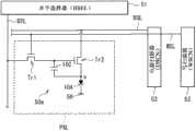
图1示出了根据本发明的第一实施方式的显示装置(有机EL显示装置1A)的截面结构。有机EL显示装置1A包括:例如通过有源矩阵驱动来驱动的多个像素(有机EL元件10A)。应注意,图1仅示出对应于一个像素(子像素)的区域。在有机EL显示装置1A中,例如,晶体管10B和电容保持元件10C设置在基板10上,且有机EL元件10A设置在这些部件上。有机EL元件10A是通过例如保护层(钝化层)22密封的,且密封基板23附着到保护层22上,其间介有未示出的粘接层。发光型的有机EL显示装置1A可以是所谓的顶发光型或底发光型。有机EL元件10A、晶体管10B和电容保持元件10C中每一个的结构在下面具体说明。FIG. 1 shows a cross-sectional structure of a display device (organic
[有机EL元件10A][
有机EL元件10A在第一电极18上具有像素隔离膜19,该像素隔离膜具有用于各个像素的开口,并在像素隔离膜19的开口中具有有机层20。第二电极21设置在有机层20上。The
例如,为每个像素设置用作阳极的第一电极18。在底发光型中,第一电极18由透明导电膜构成,例如包括氧化铟锡(ITO)、氧化铟锌(IZO)和氧化铟锌(InZnO)中的一种的单层膜或包括其中两种以上的堆叠膜。在顶发光型中,第一电极18由包括包含铝(Al)、镁(Mg)、钙(Ca)和钠(Na)中的一种以上的金属单质的单层膜,或包含一种以上金属的合金的单层膜,或包含两个以上单层膜的多层膜而构成。For example, the first electrode 18 serving as an anode is provided for each pixel. In the bottom emission type, the first electrode 18 is composed of a transparent conductive film, for example, a single-layer film including one of indium tin oxide (ITO), indium zinc oxide (IZO) and indium zinc oxide (InZnO) or both of them. More than one stacked membrane. In the top emission type, the first electrode 18 is composed of a single-layer film containing more than one metal element in aluminum (Al), magnesium (Mg), calcium (Ca) and sodium (Na), or contains more than one metal element. A single-layer film of a metal alloy, or a multi-layer film consisting of two or more single-layer films.
像素隔离膜19限定每个像素的发光区域,并包括例如光敏树脂,如聚酰亚胺树脂、丙烯酸树脂和酚醛树脂。The
有机层20包括有机电致发光层(有机EL层),并响应于所施加的驱动电流而发光。有机层20例如以靠近基板10的顺序包括例如空穴注入层、空穴传输层、有机EL层和电子传输层,上述所有均未被示出。在有机EL层中,由于所施加的电场,电子和空穴复合以导致发光。有机EL层的材料通常可包括低分子或高分子有机材料而不受任何限制。例如,可为每个像素分别涂覆红色、绿色和蓝色的彩色发光层,或者可在基板的整个表面上设置白色发光层(例如,红色、绿色和蓝色的堆叠彩色发光层)。空穴注入层改善空穴注入效率,并防止漏电。空穴传输层改善对有机EL层的空穴传输效率。根据需要,可设置有机EL层以外的这些层。The
用作阴极的第二电极21由金属导电膜构成。在底发光型中,第二电极21由包括包含铝、镁、钙和钠中的一种以上的金属单质,或包括包含一种以上金属的合金的单层膜,或作为两个以上单层膜的堆叠体的多层膜而构成。在顶发光型中,第二电极21例如包括包含ITO或IZO的透明导电膜。第二电极21对于所有像素公共地设置有机层20上,同时与第一电极18绝缘。The
保护层22可由绝缘材料或导电材料构成。绝缘材料例如包括非晶硅(a-Si)、非晶碳化硅(a-SiC)、非晶氮化硅(a-Si1-xNx)和非晶碳(a-C)。The
基板10和密封基板23均包括:例如包括石英、玻璃、硅和塑料的片材。允许使用廉价的塑料膜用于基板,因为半导体层11是通过下述溅射处理沉积的而无需加热基板10。塑料材料例如包括聚对苯二甲酸乙二醇酯(PET)和聚萘二甲酸乙二醇酯(PEN)。可选地,根据目的可使用包括不锈钢(SUS)的金属基板。在顶发光型中,密封基板23包括包含玻璃或塑料的透明基板,并可以在其上具有未示出的滤色片或遮光膜。在底发光型中,基板10包括透明基板。Both the
[晶体管10B][
晶体管10B例如对应于下述像素驱动电路50a中的采样晶体管Tr1或驱动晶体管5B,并且是具有错层结构(staggered structure)的薄膜晶体管,或所谓的顶栅薄膜晶体管。晶体管10B具有在基板10上的半导体基板11,并具有在半导体层11中的选择性区域上的栅电极13A,其间介有栅极绝缘膜12A。层间绝缘膜15设置为覆盖半导体层11、栅极绝缘膜12A和栅电极13A。层间绝缘膜15具有被配置为与半导体层11相对的接触孔H1,且源/漏电极层16设置在层间绝缘膜15上,以填充接触孔H1。因此,源/漏电极层16电连接至半导体层11的预定区域(下述源/漏区11SD)。The
在该实施方式中,半导体层11被设置为从晶体管10B到电容保持元件10C。具体地,在半导体层11中,对应于晶体管10B的部分对应于“第二半导体层”,并且对应于电容保持元件10C的部分对应于“第一半导体层”。半导体层11对应于“第一半导体层”和“第二半导体层”一体设置的结构的具体实例。In this embodiment mode, the
半导体层11响应于所施加的栅极电压形成沟道,并包括例如包含铟(In)、镓(Ga)、锌(Zn)、硅(Si)和锡(Sn)中的一种以上的氧化物半导体。这样的氧化物半导体包括例如非晶氧化物半导体,如铟锡锌氧化物(ITZO)和铟镓锌氧化物(IGZO,InGaZnO)。此外,氧化物半导体包括包含氧化锌(ZnO)、铟锌氧化物(IZO)、铟镓氧化物(IGO)、ITO和氧化铟(InO)的晶体氧化物半导体。半导体层11具有作为与源/漏电极层16的连接区域的源/漏区11SD,该源/漏区与栅电极13A相对的区域(沟道区11A)邻近。例如,半导体层11的厚度约为50nm。应注意,半导体层11在不与栅电极13A和电容保持元件10C相对的区域的在该半导体层的顶侧上的部分中具有电阻比其他区域的电阻低的低电阻区。The
从顶部以深度方向设置在半导体层11的一部分中的源/漏区11SD的电阻比沟道区11A低。源/漏区11SD的这样的低电阻是通过下述制造处理过程中通过金属的反应在氧化物半导体中扩散诸如铝的金属而提供的。结果,晶体管10B具有所谓的自对准结构并具有稳定的特性。The source/drain region 11SD provided in a part of the
栅极绝缘膜12A例如包括:包括氧化硅(SiOx)、氮化硅(SiNx)、氧氮化硅(SiON)和氧化铝(AlOx)中之一的单层膜,或包括两个以上单层膜的堆叠膜。其中,氧化硅膜或氧化铝膜是优选的,因为其几乎不会使氧化物半导体脱氧。栅极绝缘膜12A的厚度例如是约300nm。在该实施方式中,因为电容保持元件10C的栅极绝缘膜12A和绝缘膜12B由相同材料在同一步骤中形成,栅极绝缘膜12A的厚度基本与绝缘膜12B的厚度相同。这反映在栅极绝缘膜12A的厚度的设置中,因为电容保持元件10C的电容取决于绝缘膜12B的厚度。The
栅电极13A对晶体管10B施加栅极电压(Vg)从而控制半导体层11中的载流子密度,并用作提供电位至晶体管的配线。栅电极13A包括:例如包含钼(Mo)、钛(Ti)、铝、银、钕(Nd)和铜(Cu)中的一种的金属单质或合金,或包含其中两种以上的堆叠膜。特别地,栅电极13A包括诸如铝或银的低电阻金属被钼或钛所夹持的堆叠结构,或包括铝和钕的合金(AlNd合金)。可选地,栅电极13A可由诸如ITO的透明导电膜构成。栅电极13A的厚度例如为约10nm到500nm,包括10nm和500nm。The
层间绝缘膜15例如具有约2μm的厚度,并例如包括包含氧化硅膜、氮化硅膜、氧氮化硅膜和氧化铝膜中的一种的单层膜、或包括其中两种以上的堆叠膜。可选地,层间绝缘膜15可包括包含丙烯酸或聚酰亚胺树脂的有机绝缘膜。特别地,使用氧化硅膜和氧化铝膜的堆叠膜来抑制水渗入或扩散到半导体层11中,以改善晶体管10B的电特性和可靠性。The
源/漏电极层16用作晶体管10B的源电极或漏电极。源/漏电极层16例如具有约200nm的厚度,且包括类似于所列出的用于栅电极13A或类似的透明导电膜的金属。例如,优选地,源/漏电极层16由诸如铝或铜的低电阻金属构成,更优选地由这样的低电阻金属被包括钛或钼的阻挡层所夹持的堆叠膜构成。使用这类堆叠膜能够减少驱动中的配线延迟。所期望的是,源/漏电极层16设置在栅电极13A的正上方的部分之外的区域中,以防止在栅电极13A和源/漏电极层16的交叉区域中形成寄生电容。The source/
平坦化膜17被设置为覆盖层间绝缘膜15和源/漏电极层16。平坦化膜17例如包括聚酰亚胺或丙烯酸类树脂,并设置在整个显示区域上。然而,平坦化膜17具有将晶体管10B的源/漏电极层16电连接至有机EL元件10A的第一电极18的接触孔H2。第一电极18设置在平坦化膜17上以填充接触孔H2。A
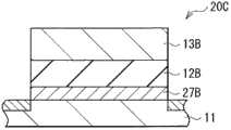
[电容保持元件10C][
例如,电容保持元件10C保持对应于下述像素电路50a中的视频信号的电荷。图2示出了电容保持元件10C的放大截面结构。由于使用晶体管10B的半导体层11的一部分的堆叠结构,电容保持元件10C具有一定电容。详细地,电容保持元件10C以靠近基板10的顺序具有导电膜27A、半导体层11、绝缘膜12B和导电膜13B的堆叠结构。在该实施方式中,导电膜27A设置在半导体层11的下方(在靠近基板10的区域上)。在电容保持元件10C中,半导体层11从晶体管10B延伸(与晶体管10B一体设置),并且导电膜27A、绝缘膜12B和导电膜13B设置在与晶体管10B分离的选择性区域中。For example, the
应注意,电容保持元件10C的导电膜27A对应于本发明的第一显示装置的“第一导电膜”的具体实例,并且导电膜13B对应于其“第二导电膜”的具体实例。It should be noted that the
例如,绝缘膜12B由与晶体管10B的栅极绝缘膜12A相同的材料形成,并且与栅极绝缘膜12A在同一步骤中形成。类似地,例如,导电膜13B由与栅电极13A相同的材料形成,并且与栅电极13A在同一步骤中形成。For example, the insulating
导电膜27A包括例如包含铝、钼和钛中的一种的单层膜,或包括其中两种以上的堆叠膜,并且具有的厚度例如为约50nm。在该实施方式中,如下文所详细描述的,导电膜27A在形成半导体层11之前形成。The
[高电阻膜14][High resistance film 14]
高电阻膜14被设置为覆盖电容保持元件10C、晶体管10B的栅极绝缘膜12A和栅电极13A、半导体层11上的不与栅电极13A和电容保持元件10C中的每一个相对的区域(低电阻区)。高电阻膜14的与源/漏电极层16相对的一部分被选择性地去除。The high-
高电阻膜14是从金属膜变化得到的氧化物膜,其用作下述制造处理过程中扩散到半导体层11的低电阻区(例如,源/漏区11SD)中的金属的供应源。这样的高电阻膜14例如包括氧化钛、氧化铝、氧化铟和氧化锡。高电阻膜14具有对外部气氛的高阻挡性能,因此具有减小氧和水的影响的功能,这样,除了上述制造处理中的功能,还可改变晶体管10B的半导体层11的电特性。高电阻膜14稳定晶体管10B和电容保持元件10C中的每一个的电特性,这增强了层间绝缘膜15的效果。高电阻膜14的厚度例如为20nm以下。High-
[外围电路和像素电路的结构][Structure of Peripheral Circuit and Pixel Circuit]
现在将说明上述有机EL显示装置1A的外围电路和像素电路的结构。图3示出了有机EL显示装置1A及其外围电路的整体结构。例如,如图所示,包括有机EL元件10A的多个像素PXL以矩阵形式配置的显示区域50设置在基板10上,并且作为信号线驱动电路的水平选择器(HSEL)51、作为扫描线驱动电路的写入扫描器(WSCN)52、乙级作为电源线驱动电路的电源扫描器(DSCN)53设置在显示区域50的外围。The structures of the peripheral circuits and the pixel circuits of the organic
在显示区域50中,多个(整数n)信号线DTL1至DTLn沿列方向配置,且多个(整数m)扫描线WSL1至WSLm和多个电源线DSL1至DSLm沿行方向配置。每个像素PXL(对应于R、G和B的像素中的一个)设置在各信号线DTL和各扫描线WSL的交叉部。每个信号线DTL连接到将视频信号提供到每个扫描线DTL的水平选择器51。每个扫描线WSL连接到将扫描信号(选择脉冲)提供到每个扫描线WSL的写入扫描器52。每个电源线DSL连接到将电源信号(控制脉冲)提供到每个电源线DSL的电源扫描器53。In the
图4具体示出了像素PXL的示例性电路结构。每个PXL具有包括有机EL元件10A的像素电路50a。像素电路50a是有源驱动电路,其包括采样晶体管Tr1、驱动晶体管Tr2、电容保持元件10C和有机EL元件10A。采样晶体管Tr1(或驱动晶体管Tr2)对应于上述实施方式等中的晶体管10B。FIG. 4 specifically shows an exemplary circuit structure of the pixel PXL. Each PXL has a
采样晶体管Tr1的栅极连接到相应的扫描线WSL,其源极和漏极中的一个连接到相应的信号线DTL,而另一个连接到驱动晶体管Tr2的栅极。驱动晶体管Tr2的漏极连接到相应的电源线DSL,且其源极连接到有机EL元件10A的阳极。有机EL元件10A的阴极连接到地线5H。应注意,地线5H公共地配线至所有像素PXLC。电容保持元件10C设置在驱动晶体管Tr2的源极和栅极之间。The gate of the sampling transistor Tr1 is connected to the corresponding scanning line WSL, one of its source and drain is connected to the corresponding signal line DTL, and the other is connected to the gate of the driving transistor Tr2. The drain of the driving transistor Tr2 is connected to the corresponding power supply line DSL, and the source thereof is connected to the anode of the
采样晶体管Tr1响应于从扫描线WSL提供的扫描信号(选择脉冲)而导通,因而对从信号线DTL提供的视频信号的信号电位进行采样,并保持电容保持元件10C中的信号电位。驱动晶体管Tr2从设定为预定的第一电位(未示出)的电源线DSL接收电流,并根据保持在电容保持元件10C中的信号电位将驱动电流提供到有机EL元件10A。有机EL元件10A响应于从动晶体管Tr2提供的驱动电流以根据视频信号的信号电位的亮度发光。The sampling transistor Tr1 is turned on in response to a scan signal (selection pulse) supplied from the scan line WSL, thus samples the signal potential of the video signal supplied from the signal line DTL, and holds the signal potential in the
在这种电路结构中,采样晶体管Tr1响应于从扫描线WSL提供的扫描信号(选择脉冲)导通,因此对从信号线DTL提供的视频信号的信号电位进行采样并保持在电容保持元件10C中。将电流从设定为第一电位的电源线DSL提供到驱动晶体管Tr2,并根据保持在电容保持元件10C中信号电位将驱动电流提供给有机EL元件10A(红色、绿色和蓝色有机EL元件中的每一个)。每个有机EL元件10A响应于所提供的驱动电流、以基于视频信号的信号电位的亮度发光。因此,显示装置基于视频信号显示视频图像。In this circuit configuration, the sampling transistor Tr1 is turned on in response to the scanning signal (selection pulse) supplied from the scanning line WSL, and thus the signal potential of the video signal supplied from the signal line DTL is sampled and held in the
[制造方法][Manufacturing method]
例如,上述有机EL显示装置1A以下列方式制造。首先,在基板10上形成晶体管10B和电容保持元件10C。For example, the above-mentioned organic
具体地,首先,如图5A所示,通过例如溅射处理在基板10的整个表面上沉积包括上述材料的导电膜27A。然后,如图5B所示,导电膜27A通过例如光刻和蚀刻被图案化而设置在基板10的选择性区域(电容形成区域)上。Specifically, first, as shown in FIG. 5A , a
然后,如图6A所示,沉积包括上述氧化物半导体的半导体层11。详细地,如图6A所示,半导体层11通过例如溅射处理沉积在基板10的整个表面上并覆盖导电膜27A。在这种沉积中,具有与目标氧化物半导体相同成分的陶瓷用作靶材。因为氧化物半导体中的载体浓度显著依赖于溅射过程中的氧分压,所以控制氧分压以实现所需的晶体管特征。然后,半导体层11通过例如光刻和蚀刻图案化为预定形状。在图案化时,半导体层11优选利用磷酸、硝酸和乙酸混合溶液通过湿蚀刻来处理。磷酸、硝酸和乙酸混合溶液可以显著增加半导体层相对于基板的蚀刻选择性,以使得较易于处理。Then, as shown in FIG. 6A ,
然后,例如通过等离子体化学气相沉积(CVD)处理在基板10的整个表面上沉积包括例如氧化硅膜的绝缘膜12(栅极绝缘膜12A和绝缘膜12B),如图6B所示。可选地,氧化硅膜可通过反应溅射处理形成。氧化铝膜不仅可以通过反应溅射处理和CVD处理而且可以通过原子层沉积处理来沉积。Then, insulating film 12 (
然后,例如钼或钛膜和铝膜的堆叠膜的导电膜13(栅电极13A和导电膜13B)通过例如溅射处理在绝缘膜12的整个表面上沉积,如图6B所示。Then, conductive film 13 (
然后,导电膜13例如通过光刻和蚀刻而图案化,从而在半导体层11中的选择性区域上形成栅电极13A和导电膜13B,如图7A所示。Then,
然后,利用栅电极13A和导电膜13作为掩膜来蚀刻绝缘膜12,如图7B所示。这里,在半导体层11由诸如ZnO、IZO和IGO的晶体材料形成的情况下,例如,可使用氢氟酸来保持大的蚀刻选择性,从而有助于蚀刻处理。因此,栅极绝缘膜12A被图案化为与栅电极13A相同的形状,且绝缘膜12B和导电膜13B形成在导电膜27A上。这样,包括导电膜27A、半导体层11、绝缘膜12B和导电膜13B的堆叠结构的电容保持元件10C在基板10的选择性区域上形成。Then, the insulating
然后,如图8A所示,通过例如溅射处理在基板10的整个表面上沉积金属膜14a,厚度为例如5nm到10nm,包括5nm和10nm,该金属膜包括在较低温度与氧反应的金属,如钛、铝和铟。Then, as shown in FIG. 8A, a
然后,如图8B所示,金属膜14a进行例如约300℃的温度的热处理以被氧化,从而形成包括金属氧化物膜的高电阻膜14。同时,在不与栅电极13A和电容保持元件10C相对的区域中形成低电阻区(包括源/漏区11SD)。因为包含在氧化物半导体中的部分氧用于金属膜14a的氧化反应,所以半导体层11中的氧浓度从其与金属膜14a接触的表面起随着金属膜14a的氧化进程而逐渐减小。此外,诸如铝的金属从金属膜14a扩散到半导体层11中。金属元素用作减小半导体层11顶部与金属膜14a接触的区域的电阻的杂质。这导致形成了具有低电阻的源/漏区域11SD。Then, as shown in FIG. 8B ,
应注意,优选金属膜14a在例如约300℃的温度通过退火进行热处理。这里,金属膜14a在例如含氧的氧化气氛中退火,这抑制了低电阻区的氧浓度的过度减小,使得能够供应充分的氧给半导体层11。因此,使得能够省略后面的退火步骤,导致处理简化。It should be noted that the
可选地,高电阻膜14可以下面的方式形成。例如,在图8A中所示的步骤中,可沉积金属膜14a,同时基板10保持约200℃的较高温度。结果,减小了半导体层11的预定区域的电阻,而无需图8B中所示的热处理。在这类情况下,半导体层11中的载流子浓度减小到晶体管所需的水平。Alternatively, high-
优选金属膜14a沉积厚度为例如10nm以下。这是因为如果金属膜14a的厚度为10nm以下,则金属膜14a通过热处理而完全氧化(形成高电阻膜14)。如果金属膜14a没有完全氧化,则这种未氧化的金属膜14a需要在额外的蚀刻步骤中去除。这是因为金属膜14a也沉积在栅电极13A上,所以如果金属膜没有充分氧化,则可能发生漏电流。如果金属膜14a完全氧化且因此形成高电阻膜14,则这样的去除步骤是不需要的,从而简化制造处理。即,无需利用蚀刻的去除步骤就可防止漏电流。应注意,在金属膜14a沉积厚度为10nm以下的情况下,热处理后高电阻膜14的厚度约为20nm以下。The
尽管金属膜14a通过上述热处理被氧化,但金属膜14a的氧化可通过诸如在蒸汽气氛中的氧化和等离子体氧化的方法加速。特别地,等离子体氧化具有下列优点。具体地,在通过金属膜14a的等离子体氧化形成高电阻膜14之后,允许通过等离子体CVD处理连续地(不断地)形成层间绝缘膜15。这消除了附加的氧化步骤。理想地,等离子体氧化在基板10的温度约为200℃到400℃(包括200℃和400℃)时,通过在例如氧和一氧化二氮(dinitroxide)的混合气体的含氧气氛中生成的等离子体进行。这是因为这种等离子体处理提供了如上所述具有对于外部环境的高阻挡性能的高电阻膜14。Although the
此外,除上述金属膜14a和半导体层11的反应之外,还可通过等离子体处理或从等离子体CVD处理沉积的氮化硅膜扩散氢来减小半导体层11的预定区域的电阻。Furthermore, in addition to the reaction of the
然后,如图9A所示,形成层间绝缘膜15。具体地,层间绝缘膜15包括上述包含丙烯酸树脂的有机膜、或包含氧化硅膜或氧化铝膜的无机膜、或有机膜和无机膜的堆叠膜,并以上述厚度沉积在高电阻膜14的整个表面上。氧化硅膜理想地通过等离子体CVD处理沉积,且氧化铝膜理想地通过使用具有铝靶的利用DC或AC电源的反应性溅射处理沉积。这是因为这样的沉积处理实现了高速沉积。有机膜通过例如旋转涂覆或狭缝涂覆而沉积。Then, as shown in FIG. 9A , an
然后,在不与半导体层11的源/漏区11SD相对的区域的一部分中例如通过光刻和蚀刻形成接触孔H1,以贯通层间绝缘膜15和高电阻膜14。Then, a contact hole H1 is formed in a part of a region not opposed to source/drain region 11SD of
如图9B所示,然后,通过例如溅射处理在层间绝缘膜15上沉积包括上述材料等的源/漏电极层16,以填充接触孔H1。然后通过光刻和蚀刻处理将源/漏电极层16图案化为预定形状。因此,形成源/漏电极层16并将其与半导体层11的源/漏区11SD电连接。如上所述,在基板10上形成了晶体管10B和电容保持元件10C。As shown in FIG. 9B , then, source/
然后,通过例如旋转涂覆或狭缝涂覆来沉积包括上述材料的平坦化膜17以覆盖层间绝缘膜15和源/漏电极层16。然后,在与源/漏电极层16相对的区域的一部分中形成接触孔H2。Then,
然后,在平坦化膜17上形成有机EL元件10A。具体地,包括上述材料的第一电极18通过例如溅射处理在平坦化膜17上形成,以填充接触孔H2,然后通过光刻和蚀刻图案化第一电极18。然后,在第一电极18上形成具有开口的像素隔离膜19,且通过例如真空蒸发处理沉积有机层20。然后,通过溅射处理在有机层20上沉积包括上述材料的第二电极21。然后,通过例如CVD处理在第二电极21上沉积保护层22,然后将密封基板23附着到保护层22上。图1中所示有机EL显示装置1的制造处理至此结束。Then, the
[操作和效果][Operation and effect]
在第一实施方式的有机EL显示装置1A中,例如,当对应于每种色彩的视频信号的驱动电流施加到对应于R、G和B之一的每个像素时,电子和空穴分别通过第一和第二电极18和21注入到有机层20中。电子和空穴在有机层20的有机EL层中复合,导致发光。以该方式,有机EL显示装置1A例如执行R、G和B的全色视频显示。In the organic
在有机EL显示装置1A中,对应于视频信号的电位在上述视频显示操作过程中施加到电容保持元件10C的一端,以使得对应于视频信号的电荷累积在电容保持元件10C中。在该实施方式中,如上所述,电容保持元件10C具有堆叠结构,其中包含氧化物半导体的半导体层11和绝缘膜12B夹在导电膜27A和导电膜13B之间。In the organic
图10示出了根据该实施方式的比较例(比较例1)的电容保持元件100的堆叠结构。在比较例1中,例如,绝缘膜102由基板101上晶体管的栅极绝缘膜的一部分形成,且在绝缘膜102上(在与晶体管的栅电极相同的层中)设置导电膜103。在导电膜103上设置具有大厚度的层间绝缘膜104,且在层间绝缘膜104上在与源/漏电极层相同的层中设置导电膜105。以该方式,比较例1的电容保持元件100具有以下结构,其中层间绝缘膜104夹在导电膜103和105之间,导电膜103和105分别设置在与晶体管的栅电极和源/漏电极相同的层中。电容也允许通过这样的堆叠结构形成。然而,在这样的电容保持元件100中,层间绝缘膜104的厚度较大(微米级尺寸),且因此电容小,导致对寄生电容的灵敏度较高。FIG. 10 shows a stacked structure of a
在第一实施方式中,电容保持元件10C具有半导体层11和绝缘膜12B夹在导电膜27A和导电膜13B之间的堆叠结构。因此,半导体层11和绝缘膜12B的总厚度小于层间绝缘膜15的厚度。结果,该实施方式的电容保持元件10C与比较例1相比具有较大电容。In the first embodiment, the
图11A和图11B示出了根据第一实施方式的另一比较例(比较例2)的电容保持元件100A的堆叠结构。在电容保持元件100A中,导电膜103设置在半导体层101上,其间介有由栅极绝缘膜形成的绝缘膜102,并且通过这样的堆叠结构提供了一定电容。虽然如同在第一实施方式中那样,这种电容保持元件100A实现了较大的电容,但电容容易根据在半导体层101与导电膜103之间施加的电压而变化。这样的电容变化可能导致根据像素电路的驱动条件的电容不足,从而导致图像质量降低。11A and 11B show a stacked structure of a
在该实施方式中,电容保持元件10C具有导电膜27A设置在半导体层11的下方,并且半导体层11和绝缘膜12B夹在导电膜27A和由栅电极13A形成的导电膜13B之间的结构。提供到电容保持元件10C的电压被保持在导电膜27A和导电膜13B之间(而不是半导体层11),这减小了根据所施加的电压的电容变化。In this embodiment,
在第一实施方式中,如上所述,与有机EL元件10A和晶体管10B一起设置在基板10上的电容保持元件10C具有堆叠结构,在该堆叠结构中包括氧化物半导体的半导体层11和绝缘膜12B(包括与栅极绝缘膜12A的材料相同的材料)夹在导电膜27A和导电膜13B(包括与栅电极13A的材料相同的材料)之间。这抑制了电容保持元件10C的电容根据所施加的电压变化,以保持所需的电容,从而抑制图像质量的降低。In the first embodiment, as described above, the
此外,这使得有源驱动显示器显示高质量图像,从而实现大画面、高分辨率和高帧率。此外,由于电容保持元件10C具有较大电容,所以可减小像素布局中的配线的占据率,从而以高产量制造具有较少数量缺陷的显示面板。In addition, this enables active-driven displays to display high-quality images, enabling large screens, high resolutions, and high frame rates. In addition, since the
[第二实施方式][Second Embodiment]
图12示出了根据本发明的第二实施方式的显示装置(有机EL显示装置1B)的截面结构。如同第一实施方式中的有机显示装置1A那样,有机EL显示装置1B包括例如通过有源矩阵驱动而驱动的多个像素(有机EL元件10A),以及驱动像素用于显示的晶体管10B和电容保持元件10C驱动。每个有机EL元件10A被保护层22和密封基板23密封。每个晶体管10B是具有包括氧化物半导体的半导体层11的顶栅薄膜晶体管。应注意,与第一实施方式中的元件相似的元件由相同的附图标记表示,并且适当地省略其说明。FIG. 12 shows a cross-sectional structure of a display device (organic
[结构][structure]
电容保持元件10C保持对应于如上文在第一实施方式中所述的像素电路50a中的视频信号的电荷。图13示出电容保持元件20C的放大截面结构。虽然电容保持元件20C由晶体管10B的堆叠结构的一部分形成,但是电容保持元件20C具有与第一实施方式的第一电容保持元件10C不同的堆叠结构。详细地,在电容保持元件20C中,半导体层11、导电膜27B、绝缘膜12B和导电膜13B以靠近基板10的顺序堆叠。即,导电膜27B设置在半导体层11上或在其上方(在靠近绝缘膜12B的区域)。具体地,在电容保持元件20C中,导电膜27B、绝缘膜12B和导电膜13B以所述顺序设置在半导体层11的选择性区域上,并且由于绝缘膜12B夹在导电膜27B和导电膜13B之间的堆叠结构而提供了一定电容。The
应注意,电容保持元件20C的导电膜27B对应于本发明的第二显示装置的“第一导电膜”的具体实例,并且导电膜13B对应于其“第二导电膜”的具体实例。It should be noted that the
在这种结构中,绝缘膜12B同样由例如与晶体管10B的栅极绝缘膜12A的材料相同的材料形成,并且与其在同一步骤中形成。类似地,导电膜13B由例如与栅电极13A的材料相同的材料形成,并且与其在同一步骤中形成。In this structure as well, the insulating
导电膜27B包括例如包含钛、铝和钼中的一种的单层膜,或包括其中的两种以上的堆叠膜,并且具有的厚度为例如约50nm。在该实施方式中,导电膜27B在形成半导体层11之后形成。The
例如,上述有机电致发光显示装置1B按以下方法制造。首先在基板10上形成晶体管10B和电容保持元件20C。具体地,首先,如图14A所示,通过例如溅射处理在基板10上沉积半导体层11,然后,通过光刻或任何其他处理将其图案化为预定形状。然后,包括上述材料等的导电膜27B通过例如溅射处理沉积在基板10的整个表面上。For example, the above-mentioned organic
然后,如图14B所示,导电膜27B通过光刻和蚀刻而被图案化从而被设置在半导体层11的选择性区域上。在蚀刻过程中,需要选择性地去除导电膜27B而不蚀刻半导体层11。例如,在利用磷酸/乙酸/硝酸的溶液来对导电膜27B进行湿蚀刻的情况下,理想地,将晶体铟镓氧化物(IGO)或铟锌氧化物(IZO)、或非晶铟锡锌氧化物(ITZO)用于半导体层11。在将铟锡锌氧化物(ITZO)用于半导体层11的情况下,通过导电膜27B的干蚀刻处理实现导电膜27B对半导体层11的高蚀刻选择性。利用磷酸/乙酸/硝酸蚀刻的导电膜27B的材料例如包括钛、钼和铝。Then, as shown in FIG. 14B , the
如图15A所示,通过与第一实施方式相似的处理在基板10的整个表面上沉积包含例如氧化硅膜或氧化铝膜的绝缘膜12(栅极绝缘膜12A和绝缘膜12B)。然后,通过与第一实施方式相似的处理在绝缘膜12的整个表面上沉积导电膜13(栅电极13A和导电膜13B)。As shown in FIG. 15A , insulating film 12 (
然后,如图15B所示,通过与第一实施方式相似的处理使导电膜13图案化(形成栅电极13A和导电膜13B),然后对绝缘膜12进行蚀刻。此处,如第一实施方式中那样,在半导体层11由诸如ZnO、IZO和IGO的晶体材料形成的情况下,使用诸如氢氟酸的腐蚀剂从而促进蚀刻处理。因此,栅极绝缘膜12A被图案化为与栅电极13A基本相同的形状,并且绝缘膜12B和导电膜13B形成在导电膜27B上。这样,在半导体层11的选择性区域上形成了包括导电膜27B、绝缘膜12B和导电膜13B的堆叠结构的电容保持元件20C。Then, as shown in FIG. 15B , the
以上述方式形成电容保持元件20C,然后如第一实施方式中那样,在基板10的整个表面上沉积金属膜14a(未示出)。然后,通过例如热处理形成高电阻膜14,并且在半导体层11的顶侧上的预定区域中形成源极/漏极区11SD。然后,如第一实施方式中那样形成层间绝缘膜15和源极/漏电极层16,从而形成了晶体管10B。如第一实施方式中那样,在基板10(其上以上述方式形成有晶体管10B和电容保持元件20C)上形成平坦化膜17、有机电致发光元件10A和保护层22,然后将密封基板23附着到保护层22上。图12中所示有机电致发光显示装置1B的制造处理至此结束。Capacitance holding
[操作和效果][Operation and effect]
在第二实施方式的有机电致发光显示装置1B中,如在第一实施方式的有机电致发光显示装置1A中那样,当对应于各颜色的视频信号的驱动电流通过第一电极18和第二电极21施加到每个像素上时,有机层20发光。这导致了例如R、G和B的全色彩视频显示。在这个过程中,对应于视频信号的电位施加到电容保持元件20C的一端,使得在电容保持元件20C中累积电荷。此处,电容保持元件20C具有这样的堆叠结构,其中,具有较小的厚度的绝缘膜12B夹在导电膜27B和导电膜13B之间,实现了较大的电容。结果,减小了寄生电容的影响。此外,电容保持元件20C具有以下结构,其中,由栅极绝缘膜12A形成的绝缘膜12B夹在导电膜27B和由栅电极13A形成的导电膜13B之间。提供到电容保持元件20C的电压被保持在导电膜27A和导电膜13B之间而不是半导体层11中,这减小了根据所施加的电压的电容变化。In the organic
在第二实施方式中,如上所述,与有机电致发光元件10A和晶体管10B一起设置在基板10上的电容保持元件20C具有绝缘膜12B(包含与栅极绝缘膜12A的材料相同的材料)夹在导电膜27B和导电膜13B(包含与栅电极13A的材料相同的材料)之间的堆叠结构。如在第一实施方式中那样,这抑制了电容保持元件20C的电容根据所施加的电压而变化,从而保持了所需的电容。因此,实现了与第一实施方式中相同的效果。In the second embodiment, as described above, the
此外,第二实施方式的电容保持元件20C在半导体层11上或在其上方具有导电膜27B,因此具有仅绝缘膜12B夹在导电膜27B与13B之间的堆叠结构,这与第一实施方式的电容保持元件10C不同。结果,电容保持元件20C具有比第一实施方式的电容保持元件10C更大的电容,从而更有效地减小了寄生电容的影响。Furthermore, the
[修改例][Modification example]
现在描述根据本发明的修改例的显示装置(液晶显示装置2)。图16示出了液晶显示装置2的截面结构。如第一实施方式中的有机EL显示装置1A那样,液晶显示装置2包括基板10上的显示元件、晶体管10B和电容保持元件10C,但显示元件是液晶显示元件20A而非有机EL元件。具体地,在液晶显示装置2中,晶体管10B和电容保持元件10C设置在基板10上,并且液晶显示元件20A设置在它们上或者它们的上方。背光30设置在基板10的下方。偏光板28a和28b分别附着到基板10的背光30侧以及密封基板23上。应注意,与这些实施方式中相似的部件以相同符号表示,并适当省略其说明。此外,尽管通过第一实施方式中描述的电容保持元件10C例示了修改例,但其也可以通过第二实施方式中描述的电容保持元件20C来例示。A display device (liquid crystal display device 2 ) according to a modified example of the present invention will now be described. FIG. 16 shows a cross-sectional structure of the liquid
在液晶显示元件20A中,例如,液晶层25A被封闭在像素电极29和对向电极26之间,且对准膜24a和24b设置在像素电极29和对向电极26的面向液晶层25的各个表面上。例如,为每个像素设置像素电极29,并且像素电极29电连接至晶体管10B的源/漏电极层16。例如,对向电极26对于多个像素公共地设置,并保持在公共电位。液晶层25包括例如以垂直对准(VA)模式、扭转向列(TN)模式或面内切换(IPS)模式驱动的液晶。In the liquid
背光30是将光发射到液晶层25的光源,并例如包括例如多个发光二极管(LED)或冷阴极荧光灯(CCFL)。背光30由未示出的背光驱动部件控制开或关。The
偏光板28a和28b(偏光镜和分析仪)例如以交叉尼科尔(crossed-Nicol)方式设置,从而在未施加电压时阻挡从背光30照射的光(关闭),并在施加电压时使其透过(打开)。The
在这种液晶显示装置2中,如第一实施方式的有机EL显示装置1A中那样,电容保持元件10C具有半导体层11和绝缘膜12B夹在导电膜27A和13B之间的堆叠结构。因此,修改例的电容保持元件10C也具有较大的电容,且减小了电容对的电压依赖性。特别地,本发明的显示装置不仅可应用到上述有机EL显示装置1A,而且可应用到液晶显示装置2。In such a liquid
[应用例][Application example]
以下,将说明上述显示装置(有机EL显示装置1和液晶显示装置2)应用到电子设备的实例。电子设备例如包括电视设备、数码相机、笔记本个人计算机、如移动电话的移动终端装置以及视频摄像机。换句话说,上述显示装置可应用于不同领域的电子设备,以将外部接收或内部生成的视频信号显示为静态或视频图像。Hereinafter, an example in which the above-described display devices (the organic
[模块][module]
各显示装置例如作为图17中所示的模块内置在诸如下述应用例1到5的各种电子设备中。在模块中,例如,基板10的一侧具有从密封基板23暴露的区域210,并且通过延伸水平选择器51、写入扫描器52和电源扫描器53的配线,将外部连接端子(未示出)设置在暴露区域210上。外部连接端子可以附有柔性印刷电路(FPC)220,以用于输入/输出信号。Each display device is built, for example, as a module shown in FIG. 17 in various electronic devices such as application examples 1 to 5 described below. In the module, for example, one side of the
[应用例1][Application example 1]
图18示出了电视设备的外观。电视设备例如具有包括前面板310和滤光玻璃320的图像显示画面部300,且图像显示画面部300对应于上述显示装置。Fig. 18 shows the appearance of a television device. The television apparatus has, for example, an image
[应用例2][Application example 2]
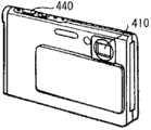
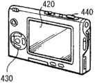
图19A和图19B示出了数码相机的外观。数码相机例如具有用于闪光的发光部410、显示部420、菜单开关430和快门按钮440,且显示部420对应于上述显示装置。19A and 19B show the appearance of a digital camera. The digital camera has, for example, a
[应用例3][Application example 3]
图20示出了笔记本个人计算机的外观。笔记本个人计算机例如具有主体510、用于字母等的输入的键盘520和用于显示图像的显示部530,且显示部530对应于上述显示装置。Fig. 20 shows the appearance of a notebook personal computer. The notebook personal computer has, for example, a
[应用例4][Application example 4]
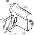
图21示出了视频摄像机的外观。视频摄像机例如具有主体部610、设置在主体部610的前侧的物体拍摄镜头620、用于拍摄的启动/停止开关630和显示部640。显示部640对应于上述显示装置。Fig. 21 shows the appearance of a video camera. The video camera has, for example, a
[应用例5][Application example 5]
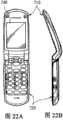
图22A至图22G示出了移动电话的外观。例如,移动电话由通过铰链部730彼此连接的上壳体710和下壳体720构成,并具有显示器740、副显示器750、画面灯760和摄像头770。显示器740或副显示器750对应于上述显示装置。22A to 22G show the appearance of the mobile phone. For example, a mobile phone is composed of an
虽然上文参考实施方式及其修改例对本发明进行了描述,但本发明不限于这些实施方式和修改例,并可做出各种其他修改或变化。例如,虽然实施方式和修改例已经通过电容保持元件10C或20C的绝缘膜12B与晶体管10B的栅极绝缘膜12A分开图案化的结构来例示,但栅极绝缘膜12A和绝缘膜12B不必分开,并且可以从晶体管10B到电容保持元件10C或20C连续设置。此外,尽管已例示了半导体层11从晶体管10B到电容保持元件10C或20C一体(连续)设置,但导体层11可以分开设置在晶体管10B和电容保持元件10C或20C的每一个中。Although the present invention has been described above with reference to the embodiments and modifications thereof, the present invention is not limited to these embodiments and modifications, and various other modifications or changes can be made. For example, although the embodiments and the modifications have been exemplified by the structure in which the insulating
此外,虽然已经以具有高电阻膜14的示例性结构对实施方式和修改例进行了描述,但可以省略高电阻膜14。然而,期望的是如上所述结构具有高电阻膜14,从而稳定地保持晶体管10B和电容保持元件10C或20C的电特性。Furthermore, although the embodiments and modifications have been described with an exemplary structure having the high-
此外,虽然实施方式和修改例中半导体层11的预定区域的电阻通过金属膜14a和半导体层11的反应减小,但是也可以通过等离子体处理、或通过从等离子体CVD处理沉积的氮化硅膜扩散氢来减小电阻。In addition, although the resistance of a predetermined region of the
通过上述本发明的示例性实施方式和修改例,至少可以实现以下结构。With the exemplary embodiments and modifications of the present invention described above, at least the following configurations can be realized.
(1)一种显示装置,包括:(1) A display device, comprising:
基板;Substrate;
显示元件;Display components;
晶体管,作为显示元件的驱动元件;以及a transistor as a driving element of the display element; and
电容保持元件,保持对应于视频信号的电荷,并且以靠近基板的顺序包括第一导电膜、包含氧化物半导体的第一半导体层、绝缘膜以及第二导电膜,其中,The capacitive holding element holds charges corresponding to video signals, and includes a first conductive film, a first semiconductor layer including an oxide semiconductor, an insulating film, and a second conductive film in order close to the substrate, wherein,
显示元件、晶体管和电容保持元件设置在基板上。Display elements, transistors and capacitive holding elements are provided on the substrate.
(2)根据(1)的显示装置,其中,晶体管以靠近基板的顺序包括:(2) The display device according to (1), wherein the transistors include, in order of proximity to the substrate:
第二半导体层,包含氧化物半导体,a second semiconductor layer comprising an oxide semiconductor,
栅极绝缘膜,设置在第二半导体层的选择性区域上,a gate insulating film disposed on a selective region of the second semiconductor layer,
栅电极,设置在栅极绝缘膜上,以及a gate electrode provided on the gate insulating film, and
源/漏电极层,电连接到第二半导体层。The source/drain electrode layer is electrically connected to the second semiconductor layer.
(3)根据(2)的显示装置,其中,第一导电膜设置在基板的选择性区域上,(3) The display device according to (2), wherein the first conductive film is provided on a selective region of the substrate,
第一半导体层和第二半导体层由相同材料一体地形成在基板上,the first semiconductor layer and the second semiconductor layer are integrally formed on the substrate from the same material,
绝缘膜由与栅极绝缘膜的材料相同的材料形成,并且the insulating film is formed of the same material as that of the gate insulating film, and
第二导电膜由与栅电极的材料相同的材料形成。The second conductive film is formed of the same material as that of the gate electrode.
(4)根据(2)或(3)的显示装置,其中,第一半导体层和第二半导体层在不与电容保持元件和栅电极这二者相对的区域中具有电阻比其他区域低的低电阻区,并且(4) The display device according to (2) or (3), wherein the first semiconductor layer and the second semiconductor layer have a lower resistance than other regions in a region not opposed to both the capacitive holding element and the gate electrode. resistance area, and
源/漏电极层电连接到低电阻区。The source/drain electrode layer is electrically connected to the low resistance region.
(5)根据(2)至(4)中任一项的显示装置,其中,高电阻膜被设置为覆盖电容保持元件、栅电极以及第一半导体层和第二半导体层的低电阻区。(5) The display device according to any one of (2) to (4), wherein the high-resistance film is provided to cover the capacitive holding element, the gate electrode, and the low-resistance region of the first semiconductor layer and the second semiconductor layer.
(6)根据(1)至(5)中任一项的显示装置,其中,显示元件是有机电致发光元件。(6) The display device according to any one of (1) to (5), wherein the display element is an organic electroluminescence element.
(7)根据(1)至(5)中任一项的显示装置,其中,显示元件是液晶显示元件。(7) The display device according to any one of (1) to (5), wherein the display element is a liquid crystal display element.
(8)一种显示装置,包括:(8) A display device, comprising:
基板;Substrate;
显示元件;Display elements;
晶体管,作为显示元件的驱动元件;以及a transistor as a driving element of the display element; and
电容保持元件,保持对应于视频信号的电荷,并且以靠近基板的顺序包括包含氧化物半导体的第一半导体层、第一导电膜、绝缘膜以及第二导电膜,其中The capacitive holding element holds charges corresponding to video signals, and includes, in order close to the substrate, a first semiconductor layer including an oxide semiconductor, a first conductive film, an insulating film, and a second conductive film, wherein
显示元件、晶体管和电容保持元件设置在基板上。Display elements, transistors and capacitive holding elements are provided on the substrate.
(9)根据(8)的显示装置,其中,晶体管以靠近基板的顺序包括:(9) The display device according to (8), wherein the transistors include, in order of proximity to the substrate:
第二半导体层,包含氧化物半导体,a second semiconductor layer comprising an oxide semiconductor,
栅极绝缘膜,设置在第二半导体层的选择性区域上,a gate insulating film disposed on a selective region of the second semiconductor layer,
栅电极,设置在栅极绝缘膜上,以及a gate electrode provided on the gate insulating film, and
源/漏电极层,电连接到第二半导体层。The source/drain electrode layer is electrically connected to the second semiconductor layer.
(10)根据(9)的显示装置,其中,第一半导体层和第二半导体层由相同材料一体地形成在基板上,(10) The display device according to (9), wherein the first semiconductor layer and the second semiconductor layer are integrally formed on the substrate from the same material,
绝缘膜由与栅极绝缘膜的材料相同的材料形成,并且the insulating film is formed of the same material as that of the gate insulating film, and
第二导电膜由与栅电极的材料相同的材料形成。The second conductive film is formed of the same material as that of the gate electrode.
(11)根据(9)或(10)的显示装置,其中,第一导电膜设置在第一半导体层的选择性区域上,并且由包括铝(Al)、钼(Mo)和钛(Ti)中的一种的单层膜或包括铝(Al)、钼(Mo)和钛(Ti)中的两种以上的堆叠膜构成,并且(11) The display device according to (9) or (10), wherein the first conductive film is provided on a selective region of the first semiconductor layer, and is composed of aluminum (Al), molybdenum (Mo) and titanium (Ti) A single-layer film of one of aluminum (Al), molybdenum (Mo) and titanium (Ti) is composed of a stacked film of two or more, and
第一半导体层和第二半导体层均包括锌铟锡氧化物(ITZO)、铟锌氧化物(IZO)、铟镓氧化物(IGO)和铟镓锌氧化物(IGZO)中的一种。Each of the first semiconductor layer and the second semiconductor layer includes one of zinc indium tin oxide (ITZO), indium zinc oxide (IZO), indium gallium oxide (IGO), and indium gallium zinc oxide (IGZO).
(12)根据(9)至(11)中任一项的显示装置,其中,第一半导体层和第二半导体层在不与电容保持元件和栅电极这二者相对的区域中具有电阻比其他区域低的低电阻区,并且(12) The display device according to any one of (9) to (11), wherein the first semiconductor layer and the second semiconductor layer have a resistance ratio higher than that of the other in a region not opposed to both the capacitive holding element and the gate electrode. region low in the low-resistance region, and
源/漏电极层电连接到低电阻区。The source/drain electrode layer is electrically connected to the low resistance region.
(13)根据(9)至(12)中任一项的显示装置,其中,高电阻膜被设置为覆盖电容保持元件、栅电极以及第一半导体层和第二半导体层的低电阻区。(13) The display device according to any one of (9) to (12), wherein the high-resistance film is provided to cover the capacitive holding element, the gate electrode, and the low-resistance region of the first semiconductor layer and the second semiconductor layer.
(14)根据(8)至(13)中任一项的显示装置,其中,显示元件是有机电致发光元件。(14) The display device according to any one of (8) to (13), wherein the display element is an organic electroluminescence element.
(15)根据(8)至(13)中任一项的显示装置,其中,显示元件是液晶显示元件。(15) The display device according to any one of (8) to (13), wherein the display element is a liquid crystal display element.
本发明包含于2011年3月31日向日本专利局提交的日本在先专利申请JP 2011-78493中所公开的主题,其全部内容结合于此作为参考。The present invention contains subject matter disclosed in Japanese Priority Patent Application JP 2011-78493 filed in the Japan Patent Office on Mar. 31, 2011, the entire content of which is hereby incorporated by reference.
本领域的技术人员应当理解,根据设计要求和其他因素,可以进行各种修改、组合、子组合和变形,只要它们在所附权利要求或其等同物的范围之内。It should be understood by those skilled in the art that various modifications, combinations, sub-combinations and alterations may occur depending on design requirements and other factors insofar as they are within the scope of the appended claims or the equivalents thereof.
Claims (18)
Applications Claiming Priority (2)
| Application Number | Priority Date | Filing Date | Title |
|---|---|---|---|
| JP2011078493AJP6019329B2 (en) | 2011-03-31 | 2011-03-31 | Display device and electronic device |
| JP2011-078493 | 2011-03-31 |
Publications (2)
| Publication Number | Publication Date |
|---|---|
| CN102738405Atrue CN102738405A (en) | 2012-10-17 |
| CN102738405B CN102738405B (en) | 2016-12-14 |
Family
ID=46926809
Family Applications (1)
| Application Number | Title | Priority Date | Filing Date |
|---|---|---|---|
| CN201210080135.4AActiveCN102738405B (en) | 2011-03-31 | 2012-03-23 | Display device and electronic equipment |
Country Status (5)
| Country | Link |
|---|---|
| US (2) | US9412763B2 (en) |
| JP (1) | JP6019329B2 (en) |
| KR (1) | KR20120112045A (en) |
| CN (1) | CN102738405B (en) |
| TW (1) | TWI552330B (en) |
Cited By (3)
| Publication number | Priority date | Publication date | Assignee | Title |
|---|---|---|---|---|
| CN104078511A (en)* | 2013-03-28 | 2014-10-01 | 索尼公司 | Semiconductor device, display unit, and electronic apparatus |
| CN104756253A (en)* | 2012-11-05 | 2015-07-01 | 索尼公司 | Semiconductor device, display unit, and electronic apparatus |
| CN106255999A (en)* | 2015-04-13 | 2016-12-21 | 株式会社半导体能源研究所 | Display panel, data processor and method for manufacturing display panel |
Families Citing this family (18)
| Publication number | Priority date | Publication date | Assignee | Title |
|---|---|---|---|---|
| JP6005401B2 (en)* | 2011-06-10 | 2016-10-12 | 株式会社半導体エネルギー研究所 | Method for manufacturing semiconductor device |
| KR102099445B1 (en) | 2012-06-29 | 2020-04-09 | 가부시키가이샤 한도오따이 에네루기 켄큐쇼 | Semiconductor device and method for manufacturing semiconductor device |
| US9246011B2 (en)* | 2012-11-30 | 2016-01-26 | Semiconductor Energy Laboratory Co., Ltd. | Semiconductor device |
| KR101996438B1 (en) | 2012-12-13 | 2019-07-05 | 삼성디스플레이 주식회사 | Substrate for display device, display device and method of manufacturing the same |
| US9905585B2 (en)* | 2012-12-25 | 2018-02-27 | Semiconductor Energy Laboratory Co., Ltd. | Semiconductor device comprising capacitor |
| WO2015033496A1 (en) | 2013-09-04 | 2015-03-12 | パナソニック株式会社 | Display device and driving method |
| JP2015108731A (en)* | 2013-12-05 | 2015-06-11 | ソニー株式会社 | SEMICONDUCTOR DEVICE, ITS MANUFACTURING METHOD, DISPLAY DEVICE, AND ELECTRONIC DEVICE |
| JP2015122417A (en)* | 2013-12-24 | 2015-07-02 | ソニー株式会社 | Semiconductor device and method of manufacturing the same, display device, and electronic apparatus |
| TWI536464B (en) | 2014-01-15 | 2016-06-01 | 友達光電股份有限公司 | Transistor and manufacturing method thereof |
| KR101877660B1 (en)* | 2014-02-28 | 2018-07-12 | 도판 인사츠 가부시키가이샤 | Lcd device |
| US9640669B2 (en) | 2014-03-13 | 2017-05-02 | Semiconductor Energy Laboratory Co., Ltd. | Semiconductor device, display device including the semiconductor device, display module including the display device, and electronic appliance including the semiconductor device, the display device, and the display module |
| TWI548067B (en) | 2014-05-22 | 2016-09-01 | 友達光電股份有限公司 | Pixel structure |
| CN110246850B (en)* | 2014-07-23 | 2022-12-02 | 索尼公司 | Display device |
| KR102412493B1 (en)* | 2015-09-08 | 2022-06-23 | 삼성디스플레이 주식회사 | Liquid crystal display device and manufacturing method thereof |
| JP6850096B2 (en)* | 2015-09-24 | 2021-03-31 | 株式会社半導体エネルギー研究所 | Manufacturing method of semiconductor devices and manufacturing method of electronic devices |
| US10109650B2 (en) | 2016-04-01 | 2018-10-23 | Joled Inc. | Semiconductor device and active matrix substrate using semiconductor device |
| KR20170119801A (en)* | 2016-04-19 | 2017-10-30 | 삼성디스플레이 주식회사 | Organic light emitting display device and method of manufacturing organic light emitting display device |
| KR102854033B1 (en)* | 2016-11-30 | 2025-09-02 | 엘지디스플레이 주식회사 | Organic light emitting diode display device |
Citations (8)
| Publication number | Priority date | Publication date | Assignee | Title |
|---|---|---|---|---|
| JP2000098409A (en)* | 1998-09-24 | 2000-04-07 | Seiko Epson Corp | Electro-optical device, method of manufacturing the same, and electronic apparatus |
| JP2001013518A (en)* | 1999-07-02 | 2001-01-19 | Sharp Corp | Liquid crystal display device and method of manufacturing the same |
| TWI256106B (en)* | 2004-04-21 | 2006-06-01 | Sharp Kk | Active matrix substrate for display device and its manufacture method |
| JP2007013013A (en)* | 2005-07-01 | 2007-01-18 | Sharp Corp | Semiconductor device, semiconductor device manufacturing method, thin film transistor array substrate, and liquid crystal display device |
| CN101196668A (en)* | 2006-12-07 | 2008-06-11 | 三菱电机株式会社 | Display device and manufacturing method thereof |
| JP2010060683A (en)* | 2008-09-02 | 2010-03-18 | Hitachi Displays Ltd | Display device |
| CN101752390A (en)* | 2008-12-05 | 2010-06-23 | 株式会社半导体能源研究所 | Semiconductor device with a plurality of semiconductor chips |
| JP2010161382A (en)* | 2007-06-29 | 2010-07-22 | Semiconductor Energy Lab Co Ltd | Semiconductor device and manufacturing method of the same |
Family Cites Families (28)
| Publication number | Priority date | Publication date | Assignee | Title |
|---|---|---|---|---|
| JP4366732B2 (en)* | 1998-09-30 | 2009-11-18 | ソニー株式会社 | Method for manufacturing electro-optical device and method for manufacturing drive substrate for electro-optical device |
| JP3763381B2 (en)* | 1999-03-10 | 2006-04-05 | シャープ株式会社 | Manufacturing method of liquid crystal display device |
| JP4700156B2 (en)* | 1999-09-27 | 2011-06-15 | 株式会社半導体エネルギー研究所 | Semiconductor device |
| US6563559B2 (en)* | 2000-02-02 | 2003-05-13 | Sanyo Electric Co., Ltd. | Reflective liquid crystal display having increase luminance for each display pixel |
| US7285459B2 (en)* | 2001-08-06 | 2007-10-23 | Samsung Sdi Co., Ltd. | Flat panel display with high capacitance and method of manufacturing the same |
| KR100930916B1 (en)* | 2003-03-20 | 2009-12-10 | 엘지디스플레이 주식회사 | Lateral electric field type liquid crystal display device and manufacturing method thereof |
| KR101039022B1 (en)* | 2004-02-11 | 2011-06-03 | 삼성전자주식회사 | Contact portion and manufacturing method thereof, thin film transistor array panel and manufacturing method thereof |
| KR101085139B1 (en)* | 2004-12-03 | 2011-11-21 | 엘지디스플레이 주식회사 | Thin film transistor array substrate and manufacturing method thereof |
| JP2007188936A (en)* | 2006-01-11 | 2007-07-26 | Epson Imaging Devices Corp | Display device |
| JP5015471B2 (en) | 2006-02-15 | 2012-08-29 | 財団法人高知県産業振興センター | Thin film transistor and manufacturing method thereof |
| JP4930704B2 (en)* | 2006-03-14 | 2012-05-16 | セイコーエプソン株式会社 | Organic electroluminescence device and electronic device |
| KR100782461B1 (en)* | 2006-04-05 | 2007-12-05 | 삼성에스디아이 주식회사 | TFT panel, manufacturing method thereof, and organic light emitting display device including the same |
| JP4723654B2 (en)* | 2006-12-22 | 2011-07-13 | シャープ株式会社 | Active matrix substrate and display panel having the same |
| US9176353B2 (en)* | 2007-06-29 | 2015-11-03 | Semiconductor Energy Laboratory Co., Ltd. | Liquid crystal display device |
| US8441007B2 (en)* | 2008-12-25 | 2013-05-14 | Semiconductor Energy Laboratory Co., Ltd. | Display device and manufacturing method thereof |
| JP2010177223A (en)* | 2009-01-27 | 2010-08-12 | Videocon Global Ltd | Liquid crystal display device and method of manufacturing the same |
| JP2010204239A (en)* | 2009-03-02 | 2010-09-16 | Seiko Epson Corp | Liquid crystal device and electronic apparatus |
| KR101041141B1 (en)* | 2009-03-03 | 2011-06-13 | 삼성모바일디스플레이주식회사 | Organic light emitting display device and manufacturing method |
| KR101668380B1 (en)* | 2009-05-19 | 2016-10-24 | 삼성디스플레이 주식회사 | Liquid crsytal display |
| KR101084233B1 (en)* | 2009-10-13 | 2011-11-16 | 삼성모바일디스플레이주식회사 | Thin film transistor and its manufacturing method |
| KR20250048807A (en)* | 2009-12-25 | 2025-04-10 | 가부시키가이샤 한도오따이 에네루기 켄큐쇼 | Semiconductor device |
| KR101084261B1 (en)* | 2010-03-17 | 2011-11-16 | 삼성모바일디스플레이주식회사 | Thin film transistor, display device having same, and manufacturing method thereof |
| KR101710179B1 (en)* | 2010-06-03 | 2017-02-27 | 삼성디스플레이 주식회사 | Flat panel display apparatus and manufacturing method of the same |
| KR20120044042A (en)* | 2010-10-27 | 2012-05-07 | 삼성모바일디스플레이주식회사 | Organic light emitting display device and method for manufacturing the same |
| KR101318601B1 (en)* | 2010-12-01 | 2013-10-15 | 샤프 가부시키가이샤 | Tft substrate and method for manufacturing tft substrate |
| JP5766481B2 (en)* | 2011-03-29 | 2015-08-19 | 株式会社Joled | Display device and electronic device |
| JP6091905B2 (en)* | 2012-01-26 | 2017-03-08 | 株式会社半導体エネルギー研究所 | Semiconductor device |
| TW201338173A (en)* | 2012-02-28 | 2013-09-16 | Sony Corp | Transistor, method of manufacturing transistor, display device and electronic machine |
- 2011
- 2011-03-31JPJP2011078493Apatent/JP6019329B2/enactiveActive
- 2012
- 2012-03-12USUS13/417,989patent/US9412763B2/enactiveActive
- 2012-03-20KRKR1020120028244Apatent/KR20120112045A/ennot_activeWithdrawn
- 2012-03-21TWTW101109668Apatent/TWI552330B/enactive
- 2012-03-23CNCN201210080135.4Apatent/CN102738405B/enactiveActive
- 2016
- 2016-07-02USUS15/201,426patent/US9721977B2/enactiveActive
Patent Citations (8)
| Publication number | Priority date | Publication date | Assignee | Title |
|---|---|---|---|---|
| JP2000098409A (en)* | 1998-09-24 | 2000-04-07 | Seiko Epson Corp | Electro-optical device, method of manufacturing the same, and electronic apparatus |
| JP2001013518A (en)* | 1999-07-02 | 2001-01-19 | Sharp Corp | Liquid crystal display device and method of manufacturing the same |
| TWI256106B (en)* | 2004-04-21 | 2006-06-01 | Sharp Kk | Active matrix substrate for display device and its manufacture method |
| JP2007013013A (en)* | 2005-07-01 | 2007-01-18 | Sharp Corp | Semiconductor device, semiconductor device manufacturing method, thin film transistor array substrate, and liquid crystal display device |
| CN101196668A (en)* | 2006-12-07 | 2008-06-11 | 三菱电机株式会社 | Display device and manufacturing method thereof |
| JP2010161382A (en)* | 2007-06-29 | 2010-07-22 | Semiconductor Energy Lab Co Ltd | Semiconductor device and manufacturing method of the same |
| JP2010060683A (en)* | 2008-09-02 | 2010-03-18 | Hitachi Displays Ltd | Display device |
| CN101752390A (en)* | 2008-12-05 | 2010-06-23 | 株式会社半导体能源研究所 | Semiconductor device with a plurality of semiconductor chips |
Cited By (7)
| Publication number | Priority date | Publication date | Assignee | Title |
|---|---|---|---|---|
| CN104756253A (en)* | 2012-11-05 | 2015-07-01 | 索尼公司 | Semiconductor device, display unit, and electronic apparatus |
| CN104078511A (en)* | 2013-03-28 | 2014-10-01 | 索尼公司 | Semiconductor device, display unit, and electronic apparatus |
| CN104078511B (en)* | 2013-03-28 | 2018-04-10 | 株式会社日本有机雷特显示器 | Semiconductor devices, display unit and electronic installation |
| CN106255999A (en)* | 2015-04-13 | 2016-12-21 | 株式会社半导体能源研究所 | Display panel, data processor and method for manufacturing display panel |
| US10831291B2 (en) | 2015-04-13 | 2020-11-10 | Semiconductor Energy Laboratory Co., Ltd. | Display panel, data processor, and method for manufacturing display panel |
| US11016329B2 (en) | 2015-04-13 | 2021-05-25 | Semiconductor Energy Laboratory Co., Ltd. | Display panel, data processor, and method for manufacturing display panel |
| US11754873B2 (en) | 2015-04-13 | 2023-09-12 | Semiconductor Energy Laboratory Co., Ltd. | Display panel, data processor, and method for manufacturing display panel |
Also Published As
| Publication number | Publication date |
|---|---|
| US9412763B2 (en) | 2016-08-09 |
| US20160315107A1 (en) | 2016-10-27 |
| US20120249904A1 (en) | 2012-10-04 |
| CN102738405B (en) | 2016-12-14 |
| US9721977B2 (en) | 2017-08-01 |
| JP6019329B2 (en) | 2016-11-02 |
| TW201248846A (en) | 2012-12-01 |
| KR20120112045A (en) | 2012-10-11 |
| TWI552330B (en) | 2016-10-01 |
| JP2012212077A (en) | 2012-11-01 |
Similar Documents
| Publication | Publication Date | Title |
|---|---|---|
| CN102738405B (en) | Display device and electronic equipment | |
| CN102738145B (en) | Display device and electronic equipment | |
| JP6111398B2 (en) | Display device and electronic device | |
| JP6111458B2 (en) | Semiconductor device, display device and electronic apparatus | |
| US20150162399A1 (en) | Semiconductor device, method of manufacturing the same, display unit, and electronic apparatus | |
| WO2014068859A1 (en) | Semiconductor device, display unit, and electronic apparatus | |
| JP6142136B2 (en) | Transistor manufacturing method, display device manufacturing method, and electronic device manufacturing method | |
| US20150179681A1 (en) | Semiconductor device, method of manufacturing the same, display unit, and electronic apparatus | |
| US20160149042A1 (en) | Semiconductor device and method of manufacturing the same, and display unit and electronic apparatus | |
| JP6019331B2 (en) | Transistor, semiconductor device, display device, electronic device, and method for manufacturing semiconductor device |
Legal Events
| Date | Code | Title | Description |
|---|---|---|---|
| C06 | Publication | ||
| PB01 | Publication | ||
| SE01 | Entry into force of request for substantive examination | ||
| SE01 | Entry into force of request for substantive examination | ||
| ASS | Succession or assignment of patent right | Owner name:JANPAN ORGANIC RATE DISPLAY CO., LTD. Free format text:FORMER OWNER: SONY CORP Effective date:20150715 | |
| C41 | Transfer of patent application or patent right or utility model | ||
| TA01 | Transfer of patent application right | Effective date of registration:20150715 Address after:Tokyo, Japan Applicant after:JOLED Inc. Address before:Tokyo, Japan Applicant before:Sony Corp. | |
| C14 | Grant of patent or utility model | ||
| GR01 | Patent grant | ||
| TR01 | Transfer of patent right | Effective date of registration:20231123 Address after:Tokyo, Japan Patentee after:Japan Display Design and Development Contract Society Address before:Tokyo Patentee before:JOLED Inc. | |
| TR01 | Transfer of patent right | ||
| TR01 | Transfer of patent right | ||
| TR01 | Transfer of patent right | Effective date of registration:20250730 Address after:Tokyo, Japan Patentee after:Magno Bolan Co.,Ltd. Country or region after:Japan Address before:Tokyo, Japan Patentee before:Japan Display Design and Development Contract Society Country or region before:Japan |