CN102738060B - A kind of preparation method of GOI wafer structure - Google Patents
A kind of preparation method of GOI wafer structureDownload PDFInfo
- Publication number
- CN102738060B CN102738060BCN201210225637.1ACN201210225637ACN102738060BCN 102738060 BCN102738060 BCN 102738060BCN 201210225637 ACN201210225637 ACN 201210225637ACN 102738060 BCN102738060 BCN 102738060B
- Authority
- CN
- China
- Prior art keywords
- layer
- substrate
- goi
- wafer structure
- preparing
- Prior art date
- Legal status (The legal status is an assumption and is not a legal conclusion. Google has not performed a legal analysis and makes no representation as to the accuracy of the status listed.)
- Active
Links
- 238000002360preparation methodMethods0.000titleclaimsabstractdescription8
- 229910000577Silicon-germaniumInorganic materials0.000claimsabstractdescription68
- 238000000034methodMethods0.000claimsabstractdescription60
- 229910052732germaniumInorganic materials0.000claimsabstractdescription43
- GNPVGFCGXDBREM-UHFFFAOYSA-Ngermanium atomChemical compound[Ge]GNPVGFCGXDBREM-UHFFFAOYSA-N0.000claimsabstractdescription42
- 230000008569processEffects0.000claimsabstractdescription38
- 238000005468ion implantationMethods0.000claimsabstractdescription18
- 238000000137annealingMethods0.000claimsabstractdescription6
- 239000000758substrateSubstances0.000claimsdescription49
- XUIMIQQOPSSXEZ-UHFFFAOYSA-NSiliconChemical compound[Si]XUIMIQQOPSSXEZ-UHFFFAOYSA-N0.000claimsdescription20
- 229910052710siliconInorganic materials0.000claimsdescription20
- 239000010703siliconSubstances0.000claimsdescription20
- WGTYBPLFGIVFAS-UHFFFAOYSA-Mtetramethylammonium hydroxideChemical compound[OH-].C[N+](C)(C)CWGTYBPLFGIVFAS-UHFFFAOYSA-M0.000claimsdescription18
- VYPSYNLAJGMNEJ-UHFFFAOYSA-NSilicium dioxideChemical compoundO=[Si]=OVYPSYNLAJGMNEJ-UHFFFAOYSA-N0.000claimsdescription16
- 238000006243chemical reactionMethods0.000claimsdescription12
- 150000002500ionsChemical class0.000claimsdescription10
- 229910004298SiO 2Inorganic materials0.000claimsdescription8
- 229910052681coesiteInorganic materials0.000claimsdescription8
- 229910052906cristobaliteInorganic materials0.000claimsdescription8
- 239000000377silicon dioxideSubstances0.000claimsdescription8
- 235000012239silicon dioxideNutrition0.000claimsdescription8
- 229910052682stishoviteInorganic materials0.000claimsdescription8
- 229910052905tridymiteInorganic materials0.000claimsdescription8
- 238000005530etchingMethods0.000claimsdescription6
- 239000012299nitrogen atmosphereSubstances0.000claimsdescription6
- 239000012298atmosphereSubstances0.000claimsdescription5
- 230000001681protective effectEffects0.000claimsdescription4
- 229910018072Al 2 O 3Inorganic materials0.000claimsdescription3
- 239000004065semiconductorSubstances0.000abstractdescription9
- 238000004519manufacturing processMethods0.000abstractdescription4
- 235000012431wafersNutrition0.000description24
- 239000000463materialSubstances0.000description8
- 239000000203mixtureSubstances0.000description8
- 238000002513implantationMethods0.000description5
- 238000007254oxidation reactionMethods0.000description5
- 238000011161developmentMethods0.000description4
- 238000010586diagramMethods0.000description4
- 230000008018meltingEffects0.000description4
- 238000002844meltingMethods0.000description4
- 239000000243solutionSubstances0.000description4
- 230000008859changeEffects0.000description3
- 230000003647oxidationEffects0.000description3
- 230000008901benefitEffects0.000description2
- 238000004140cleaningMethods0.000description2
- 230000007797corrosionEffects0.000description2
- 238000005260corrosionMethods0.000description2
- 230000000694effectsEffects0.000description2
- 238000012986modificationMethods0.000description2
- 230000004048modificationEffects0.000description2
- 238000012545processingMethods0.000description2
- 238000011160researchMethods0.000description2
- 230000004913activationEffects0.000description1
- 239000007864aqueous solutionSubstances0.000description1
- 230000009286beneficial effectEffects0.000description1
- 230000015572biosynthetic processEffects0.000description1
- 239000013078crystalSubstances0.000description1
- 230000007423decreaseEffects0.000description1
- 230000007547defectEffects0.000description1
- 238000000151depositionMethods0.000description1
- 230000008021depositionEffects0.000description1
- 238000009826distributionMethods0.000description1
- 238000000407epitaxyMethods0.000description1
- YBMRDBCBODYGJE-UHFFFAOYSA-Ngermanium oxideInorganic materialsO=[Ge]=OYBMRDBCBODYGJE-UHFFFAOYSA-N0.000description1
- 238000010438heat treatmentMethods0.000description1
- 238000009413insulationMethods0.000description1
- 239000012212insulatorSubstances0.000description1
- 230000007246mechanismEffects0.000description1
- 239000002184metalSubstances0.000description1
- 231100000252nontoxicToxicity0.000description1
- 230000003000nontoxic effectEffects0.000description1
- 230000003287optical effectEffects0.000description1
- 230000005693optoelectronicsEffects0.000description1
- PVADDRMAFCOOPC-UHFFFAOYSA-NoxogermaniumChemical compound[Ge]=OPVADDRMAFCOOPC-UHFFFAOYSA-N0.000description1
- 238000005498polishingMethods0.000description1
- 238000012827research and developmentMethods0.000description1
- 239000002210silicon-based materialSubstances0.000description1
Images


Classifications
- H—ELECTRICITY
- H01—ELECTRIC ELEMENTS
- H01L—SEMICONDUCTOR DEVICES NOT COVERED BY CLASS H10
- H01L21/00—Processes or apparatus adapted for the manufacture or treatment of semiconductor or solid state devices or of parts thereof
- H01L21/70—Manufacture or treatment of devices consisting of a plurality of solid state components formed in or on a common substrate or of parts thereof; Manufacture of integrated circuit devices or of parts thereof
- H01L21/71—Manufacture of specific parts of devices defined in group H01L21/70
- H01L21/76—Making of isolation regions between components
- H01L21/762—Dielectric regions, e.g. EPIC dielectric isolation, LOCOS; Trench refilling techniques, SOI technology, use of channel stoppers
- H01L21/7624—Dielectric regions, e.g. EPIC dielectric isolation, LOCOS; Trench refilling techniques, SOI technology, use of channel stoppers using semiconductor on insulator [SOI] technology
- H01L21/76251—Dielectric regions, e.g. EPIC dielectric isolation, LOCOS; Trench refilling techniques, SOI technology, use of channel stoppers using semiconductor on insulator [SOI] technology using bonding techniques
- H01L21/76254—Dielectric regions, e.g. EPIC dielectric isolation, LOCOS; Trench refilling techniques, SOI technology, use of channel stoppers using semiconductor on insulator [SOI] technology using bonding techniques with separation/delamination along an ion implanted layer, e.g. Smart-cut, Unibond
Landscapes
- Engineering & Computer Science (AREA)
- Physics & Mathematics (AREA)
- Condensed Matter Physics & Semiconductors (AREA)
- General Physics & Mathematics (AREA)
- Manufacturing & Machinery (AREA)
- Computer Hardware Design (AREA)
- Microelectronics & Electronic Packaging (AREA)
- Power Engineering (AREA)
- Recrystallisation Techniques (AREA)
Abstract
Translated fromChinese
Description
Translated fromChinese技术领域technical field
本发明涉及一种晶片结构的制备方法,特别是涉及一种GOI晶片结构的制备方法。The invention relates to a method for preparing a wafer structure, in particular to a method for preparing a GOI wafer structure.
背景技术Background technique
随着硅基大规模集成电路技术的飞速发展,体硅CMOS器件的性能已逐渐接近硅材料的物理极限,沿Moore定律指引的方向进一步提高体硅CMOS器件的性能将面临越来越大的投资和市场风险。半导体产业是一个对产品性能价格比十分敏感的市场。如何在现有VLSL工艺的基础上不断地提高硅基器件的性能,又不大量增加投资,成了业界的共同难题。而对新材料和新工艺的探索,无疑使解决这个问题的一个重要思路和研究方向。With the rapid development of silicon-based large-scale integrated circuit technology, the performance of bulk silicon CMOS devices has gradually approached the physical limit of silicon materials, and further improving the performance of bulk silicon CMOS devices in the direction guided by Moore's law will face increasing investment and market risk. The semiconductor industry is a market that is very sensitive to the performance-price ratio of products. How to continuously improve the performance of silicon-based devices based on the existing VLSL process without increasing investment has become a common problem in the industry. The exploration of new materials and new processes is undoubtedly an important way of thinking and research direction to solve this problem.
绝缘体上锗(GOI)是高端硅基衬底材料领域的一项最新开发成果,它对高性能CMOS IC以及光电探测器和太阳能电池都具有十分重要的意义。能用作光电探测器GOI(锗吸收850nm波长的光的效率是硅的70倍),而且也能用来制作高速晶体管。基于锗材料的晶体管的转换速度能比硅的大3到4倍。由于锗金属能提高材料的电子迁移率,在未来的高速逻辑IC应用上,锗材料远景看好。GOI用作制造高速光电探测器(运行在30GHz),这使其理论上适用于探测速度大于50Gb/sec的信号,使芯片上的光互连更接近现实。GOI技术能和硅CMOS工艺兼容,因为锗能够有选择的放置在光电探测器所在的区域,所以新的探测器与标准的微芯片技术兼容。这种兼容性使得有可能在同一块芯片上集成光电电路,比如在微处理器和其他电子器件上。目前主要被关注于以下几个领域:GOI高速CMOS器件、高频CMOS器件、光电探测器以及太阳能电池等。几十年前人们就知道了锗与硅相比所具有的速度优势;然而,锗氧化层的不稳定性使得当时制作MOS器件不太可行。如今,新一代的高k介质淀积技术,加上这些新的GOI衬底,给器件生产商在使用锗上有更多的灵活性,从而回避了MOS栅氧问题。体锗晶圆要比硅重,且易碎,GOI有助于克服这些问题,并使锗MOSFET技术与硅处理设备相兼容。应用于锗施主的外延方法可以轻易地将其等比变化至300mm,但晶体缺陷可能会很高。对锗表面进行处理是一项十分艰巨的任务,因为典型的硅清洗溶液会对锗表面造成腐蚀,使表面变得粗糙。尽管已证实可用硅加工设备对GOI进行处理,且0.15微米器件已经制作成功,但MOSFET的Ion/Ioff比值却十分不理想,而且迁移率值也需要进一步改善。锗表面上的MOSFET质量是一个问题,但由于锗的禁带宽度很小(0.66eV),所以锗器件也承受着大漏电流的致命缺点,这也严重阻碍了锗MOS器件的更广泛的应用,GOI技术必须解决由于锗较窄的带隙对结的漏泄和带-带调谐带来的影响。如同SOI解决了很多体硅在半导体器件中的不足,GOI同样也是很好地解决了Ge材料缺点的候选材料。为了得到低漏电流和更好的性能的MOS器件,GOI因此得到了关注。一些科研结构和公司通过很多方法已经制备出GOI结构,例如,欧洲半导体领域三巨头Soitec、IMEC和Umicore宣布联合开发GOI技术,Umicore侧重于研发8和12英寸单晶Ge晶片,而Soitec用Smart Cut技术研发GOI晶片,IMEC重点研究以Ge基工艺制备应用于45纳米及以下制程的高性能CMOS电路。Silicon Genesis也宣称他们正在研制GOI圆片,IBM宣布开发了一种基于新开发的GOI技术的高速光电探测器,他们制造GOI的方法是直接在很薄的SOI上生长锗。然而目前这些方法都有很多局限性,例如利用在SOI上外延的SiGe进行浓缩不仅工艺复杂,还会引入很高的位错密度(≥107),严重影响了最终GOI的质量和后期器件的性能。从穿透位错的形成机理上来讲,是由于浓缩开始时SiGe/Si界面的失配位错下降到SGOI/BOX界面,进一步浓缩,失配位错向上穿透形成了穿透位错。Germanium-on-insulator (GOI) is a recent development in the field of high-end silicon-based substrate materials, which is of great significance for high-performance CMOS ICs as well as photodetectors and solar cells. It can be used as a photodetector GOI (germanium absorbs light with a wavelength of 850nm 70 times more efficiently than silicon), and can also be used to make high-speed transistors. Transistors based on the germanium material can switch three to four times faster than silicon. Since germanium metal can improve the electron mobility of materials, germanium materials have a promising future in the application of high-speed logic ICs in the future. GOI is used to make high-speed photodetectors (operating at 30GHz), which makes it theoretically suitable for detecting signals with speeds greater than 50Gb/sec, making on-chip optical interconnections closer to reality. GOI technology is compatible with silicon CMOS processes, and because germanium can be selectively placed in the area where the photodetectors are located, the new detectors are compatible with standard microchip technology. This compatibility makes it possible to integrate optoelectronic circuits on the same chip, such as in microprocessors and other electronic devices. At present, it is mainly focused on the following fields: GOI high-speed CMOS devices, high-frequency CMOS devices, photodetectors and solar cells. The speed advantage of germanium over silicon has been known for decades; however, the instability of the germanium oxide layer made making MOS devices impractical at the time. Today, a new generation of high-k dielectric deposition technology, coupled with these new GOI substrates, gives device manufacturers more flexibility in using germanium, thereby avoiding the MOS gate oxide problem. Bulk germanium wafers are heavier than silicon and fragile, and GOI helps overcome these issues and makes germanium MOSFET technology compatible with silicon processing equipment. Epitaxy methods applied to germanium donors can easily scale this up to 300mm, but crystal defects can be high. Preparing germanium surfaces is a difficult task because typical silicon cleaning solutions corrode and roughen germanium surfaces. Although it has been proven that silicon processing equipment can be used to process GOI, and 0.15 micron devices have been successfully fabricated, the Ion / Ioff ratio of MOSFET is far from ideal, and the mobility value needs to be further improved. The quality of MOSFETs on the surface of germanium is a problem, but because of the small band gap of germanium (0.66eV), germanium devices also suffer from the fatal shortcoming of large leakage current, which also seriously hinders the wider application of germanium MOS devices , GOI technology must solve the impact of the junction leakage and band-band tuning due to the narrower bandgap of germanium. Just as SOI solves the shortcomings of many bulk silicon in semiconductor devices, GOI is also a candidate material that solves the shortcomings of Ge materials. In order to obtain MOS devices with low leakage current and better performance, GOI has thus received attention. Some scientific research institutions and companies have prepared GOI structures through many methods. For example, the three giants in the European semiconductor field, Soitec, IMEC and Umicore, announced the joint development of GOI technology. Technology research and development of GOI wafers, IMEC focuses on the preparation of high-performance CMOS circuits for 45nm and below processes using Ge-based technology. Silicon Genesis also announced that they are developing GOI wafers, and IBM announced that it has developed a high-speed photodetector based on the newly developed GOI technology. Their method of manufacturing GOI is to grow germanium directly on very thin SOI. However, these current methods have many limitations. For example, the use of epitaxial SiGe on SOI for concentration is not only complicated in process, but also introduces a high dislocation density (≥107 ), which seriously affects the quality of the final GOI and the quality of later devices. performance. From the perspective of the formation mechanism of threading dislocations, it is because the misfit dislocations at the SiGe/Si interface descend to the SGOI/BOX interface at the beginning of concentration, and further condense, and the misfit dislocations penetrate upwards to form threading dislocations.
鉴于此,如何提出一种工艺简单而又能降低GOI穿透位错密度的制备方法成为目前亟待解决的问题。In view of this, how to propose a preparation method that has a simple process and can reduce the density of GOI threading dislocations has become an urgent problem to be solved.
发明内容Contents of the invention
鉴于以上所述现有技术的缺点,本发明的目的在于提供一种GOI晶片结构的制备方法,用于解决现有技术中工艺复杂、以及GOI晶片中位错密度大的问题。In view of the above-mentioned shortcomings of the prior art, the object of the present invention is to provide a method for preparing a GOI wafer structure, which is used to solve the problems of complex processes and high dislocation density in the GOI wafer in the prior art.
为实现上述目的及其他相关目的,本发明提供一种GOI晶片结构的制备方法,其特征在于,至少包括以下步骤:In order to achieve the above purpose and other related purposes, the invention provides a method for preparing a GOI wafer structure, which is characterized in that it at least includes the following steps:
1)利用智能剥离工艺制备出SGOI结构;1) Prepare the SGOI structure by using the intelligent stripping process;
2)对所述SGOI结构进行锗浓缩,形成依次包含有第二Si衬底、绝缘埋层BOX、Ge层、SiO2层的层叠结构;2) Concentrating germanium on the SGOI structure to form a laminated structure sequentially comprising a second Si substrate, an insulating buried layer BOX, a Ge layer, and anSiO2 layer;
3)腐蚀掉所述层叠结构表面的SiO2层以得到GOI结构。3) Etching away theSiO2 layer on the surface of the laminated structure to obtain the GOI structure.
可选地,所述步骤1)还包括:Optionally, the step 1) also includes:
1-1)提供第一Si衬底,在所述第一Si衬底上外延生长一层SiGe层;1-1) providing a first Si substrate, and epitaxially growing a SiGe layer on the first Si substrate;
1-2)采用离子注入工艺从所述SiGe层表面进行H+离子注入,并控制离子注入能量在所述第一Si衬底中预设的深度形成一层富含H+离子的硅层作为剥离层;1-2) Using an ion implantation process to perform H+ ion implantation from the surface of the SiGe layer, and control the ion implantation energy to form a silicon layer rich in H+ ions at a preset depth in the first Si substrate as a peeling layer ;
1-3)提供第二Si衬底,并在所述第二Si衬底上制备一层绝缘埋层BOX;1-3) providing a second Si substrate, and preparing a layer of insulating buried layer BOX on the second Si substrate;
1-4)利用键合工艺将第一Si衬底上的SiGe层表面与第二Si衬底上的SiO2层表面进行键合形成依次包含有第二Si衬底、绝缘埋层BOX、SiGe层、第一Si衬底的层叠结构;1-4) The surface of the SiGe layer on the first Si substrate and the surface of theSiO2 layer on the second Si substrate are bonded using a bonding process to form a second Si substrate, an insulating buried layer BOX, and a SiGe layer in sequence. layer, the laminated structure of the first Si substrate;
1-5)对键合后的结构进行高温退火处理,以从所述剥离层处剥离掉部分所述第一Si衬底;1-5) performing high-temperature annealing treatment on the bonded structure, so as to peel off part of the first Si substrate from the peeling layer;
1-6)利用TMAH腐蚀液将剩余的所述第一Si衬底全部腐蚀掉以得到SGOI结构。1-6) Using TMAH etching solution to etch away all the remaining first Si substrate to obtain an SGOI structure.
可选地,所述步骤1-1)中外延生长的SiGe层的厚度为80nm~120nm,所述SiGe层中Ge的组分为12%~30%。Optionally, the thickness of the epitaxially grown SiGe layer in the step 1-1) is 80nm-120nm, and the composition of Ge in the SiGe layer is 12%-30%.
可选地,所述步骤1-2)中离子注入能量为60Kev,注入H+离子的剂量为6.0E16。进一步可选地,所述H+离子注入第一Si衬底中的深度为600nm~700nm。Optionally, the ion implantation energy in the step 1-2) is 60Kev, and the dose of implanted H+ ions is 6.0E16. Further optionally, the implantation depth of the H+ ions into the first Si substrate is 600nm˜700nm.
可选地,所述步骤1-3)中第二Si衬底上制备的绝缘埋层BOX的材质为SiO2或Al2O3。进一步可选地,所述绝缘埋层BOX的厚度为100nm~150nm。Optionally, the insulating buried layer BOX prepared on the second Si substrate in step 1-3) is made of SiO2 or Al2 O3 . Further optionally, the thickness of the buried insulating layer BOX is 100 nm˜150 nm.
可选地,所述步骤1-5)剥离掉部分所述第一Si衬底的工艺条件为:先升温到300℃,保温3小时后,再经半个小时升温到600℃后保温半小时,整个过程通有8000ccm的高纯O2。Optionally, the process conditions for peeling off part of the first Si substrate in the step 1-5 are as follows: first raise the temperature to 300°C, keep it warm for 3 hours, then raise the temperature to 600°C for half an hour, and then keep it warm for half an hour , the whole process has 8000ccm high-purity O2 .
可选地,所述步骤2)中锗浓缩工艺后形成的Ge层的厚度为7nm~50nm。Optionally, the thickness of the Ge layer formed after the germanium concentration process in step 2) is 7nm-50nm.
可选地,所述步骤2)还包括:Optionally, the step 2) also includes:
2-1)将所述SGOI结构放入600℃反应炉中,然后通入5000ccm的N2作为保护气氛,以每分钟上升10℃速度加热反应炉至于达到1050℃后停止通入N2,;2-1) Put the SGOI structure into a 600°C reaction furnace, and then pass 5000ccm of N2 as a protective atmosphere, heat the reaction furnace at a rate of 10°C per minute until it reaches 1050°C, and stop feeding N2 ;
2-2)通入4000ccm的O2保持30分钟后停止;2-2) Infuse 4000ccm of O2 for 30 minutes and then stop;
2-3)通入5000ccm的N2保持30分钟后停止;2-3) Infuse 5000ccm of N2 for 30 minutes and then stop;
2-4)重复步骤2-2)与步骤2-3)4次后,在N2气氛下使反应炉温度在1个小时内从1050℃降到900℃;2-4) After repeating step 2-2) and step 2-3) 4 times, lower the temperature of the reaction furnace from 1050°C to 900°C within 1 hour underN2 atmosphere;
2-5)通入4000ccm的O2保持30分钟后停止;2-5) Infuse 4000ccm of O2 for 30 minutes and then stop;
2-6)通入5000ccm的N2保持30分钟后停止;2-6) Infuse 5000ccm ofN2 for 30 minutes and then stop;
2-7)重复步骤2-5)与步骤2-6)4次后,在N2气氛下使反应炉温度在1个小时内从900℃降至600℃,完成锗浓缩,形成依次包含有第二Si衬底、绝缘埋层BOX、Ge层、SiO2层的层叠结构。2-7) After repeating steps 2-5) and steps 2-6) 4 times, the temperature of the reaction furnace was lowered from 900°C to 600°C within 1 hour under N2 atmosphere to complete the concentration of germanium and form the A stacked structure of two Si substrates, an insulating buried layer BOX, a Ge layer, and a SiO2 layer.
如上所述,本发明的一种GOI晶片结构的制备方法,具有以下有益效果:As mentioned above, a method for preparing a GOI wafer structure of the present invention has the following beneficial effects:
本发明首先利用Smart-Cut技术制作出SGOI晶片结构,然后对SGOI晶片结构进行锗浓缩,从而得到GOI晶片结构。由于利用Smart-Cut技术制作的SGOI在SGOI/BOX界面基本不存在失配位错,从而最终降低了GOI的穿透位错。本发明工艺简单,可实现高质量GOI晶片结构,大大改进了锗浓缩技术,另外,离子注入技术、退火技术在目前半导体行业都是非常成熟的工艺,所以这种制备方法大大提高了锗浓缩在半导体工业界广泛应用的可能性。In the present invention, the SGOI wafer structure is first produced by using the Smart-Cut technology, and then germanium is concentrated on the SGOI wafer structure to obtain the GOI wafer structure. Since the SGOI fabricated by Smart-Cut technology basically has no misfit dislocation at the SGOI/BOX interface, the threading dislocation of GOI is finally reduced. The invention has a simple process, can realize high-quality GOI wafer structure, and greatly improves the germanium concentration technology. In addition, ion implantation technology and annealing technology are very mature processes in the current semiconductor industry, so this preparation method greatly improves the germanium concentration. The possibility of wide application in the semiconductor industry.
附图说明Description of drawings
图1a~1f显示为本发明中利用智能剥离技术制备SGOI结构的工艺的流程图。Figures 1a-1f show a flow chart of the process for preparing the SGOI structure using the smart stripping technique in the present invention.
图2显示为本发明中锗浓缩后的结构示意图。Fig. 2 is a schematic diagram showing the structure of germanium after enrichment in the present invention.
图3显示为本发明中制备的最终GOI结构示意图。Figure 3 shows a schematic diagram of the final GOI structure prepared in the present invention.
元件标号说明Component designation description
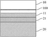
10 第一Si衬底10 The first Si substrate
100 剥离层100 Peel off layer
11 SiGe层11 SiGe layer
110 SiO2层110 SiO2 layers
20 第二Si衬底20 Second Si substrate
21 绝缘埋层BOX21 Insulation buried layer BOX
具体实施方式Detailed ways
以下通过特定的具体实例说明本发明的实施方式,本领域技术人员可由本说明书所揭露的内容轻易地了解本发明的其他优点与功效。本发明还可以通过另外不同的具体实施方式加以实施或应用,本说明书中的各项细节也可以基于不同观点与应用,在没有背离本发明的精神下进行各种修饰或改变。Embodiments of the present invention are described below through specific examples, and those skilled in the art can easily understand other advantages and effects of the present invention from the content disclosed in this specification. The present invention can also be implemented or applied through other different specific implementation modes, and various modifications or changes can be made to the details in this specification based on different viewpoints and applications without departing from the spirit of the present invention.
请参阅图1a至图1f、以及图2至图3。需要说明的是,本实施例中所提供的图示仅以示意方式说明本发明的基本构想,遂图式中仅显示与本发明中有关的组件而非按照实际实施时的组件数目、形状及尺寸绘制,其实际实施时各组件的型态、数量及比例可为一种随意的改变,且其组件布局型态也可能更为复杂。Please refer to FIGS. 1a to 1f and FIGS. 2 to 3 . It should be noted that the diagrams provided in this embodiment are only schematically illustrating the basic idea of the present invention, and only the components related to the present invention are shown in the diagrams rather than the number, shape and shape of the components in actual implementation. Dimensional drawing, the type, quantity and proportion of each component can be changed arbitrarily during actual implementation, and the component layout type may also be more complicated.
如图所示,本发明提供一种GOI晶片结构的制备方法,至少包括以下步骤:As shown in the figure, the present invention provides a method for preparing a GOI wafer structure, at least including the following steps:
首先,参考图1a至图1f,利用智能剥离技术(Smart-cut)制备出SGOI晶片结构,包括以下步骤:First, with reference to Figures 1a to 1f, the SGOI wafer structure is prepared using the Smart-cut technology, including the following steps:
步骤一:如图1a所示,提供第一Si衬底10,在所述第一Si衬底10上外延生长一层SiGe层11,其中SiGe层11的厚度为80nm~120nm,本实施例中SiGe层11的厚度选为100nm,但不限于此,在其它实施例中,SiGe层11的厚度可以根据需要来调整。此外,SiGe层11中Ge的含量为12%~30%,本实施例中暂选为30%,但不限于此,在其它实施例中,Ge的含量可以根据需要来调整,特此声明。Step 1: As shown in FIG. 1a, a
步骤二:如图1b所示,采用离子注入工艺从所述SiGe层11表面进行H+离子注入,并控制离子注入能量在所述第一Si衬底10中预设的深度形成一层富含H+离子的硅层作为剥离层100,H+注入能量越大,H+注入峰越深,一般来说,当离子注入能量为50Kev~150Kev时,对应注入Si片的深度分布在500nm~1200nm。本实施中离子注入能量为60Kev,对应从SiGe层11表面注入深度为700nm~800nm,由于SiGe层11的厚度为100nm,所以H+离子注入第一Si衬底10中的深度为600nm~700m,但不限于此,在其它实施例中,根据需要亦可以选用不同的离子注入能量以达到不同的注入深度。Step 2: As shown in FIG. 1b, perform H+ ion implantation from the surface of the
步骤三:如图1c所示,提供第二Si衬底20,并在所述第二Si衬底20上热氧化生长一层厚度为100nm~150nm的绝缘埋层BOX21,本实施例中绝缘埋层BOX21的厚度选为120nm。需要说明的是,本实施例中绝缘埋层材质暂选为SiO2,但不限于此,在其它实施例中,亦可以为Al2O3,特此声明。Step 3: As shown in FIG. 1c, provide a
步骤四:如图1d所示,将第一Si衬底片10上的SiGe层11表面与第二Si衬底20上的绝缘埋层BOX21表面进行严格的清洗、活化处理、以及抛光处理后,在室温下把两个抛光面贴合在一起使两个硅片键合在一起,形成依次包含有第二Si层20、绝缘埋层BOX21、SiGe层11、第一Si衬底10的层叠结构,其中该绝缘埋层BOX21作为最终形成结构中的绝缘埋层。Step 4: As shown in FIG. 1d, the surface of the
步骤五:如图1e所示,对键合后的结构进行退火处理。一般分两步:第一步,第一Si衬底中注入的高浓度的含H+离子的剥离层100在高温下会成核并形成气泡,气泡的急剧膨胀把硅片在富含高浓度H+离子层的剥离层100处分开,也就是发生剥离;第二步,高温热处理提高键合界面的结合强度并消除键合结构中的离子注入损伤。本实施例中的具体工艺条件为:先升温到300℃,保温3小时后,使第一Si衬底10在剥离层100处发生剥离,再经半个小时升温到600℃后保温半小时,提高键合界面的结合强度,整个过程通有8000ccm的高纯O2。Step 5: As shown in FIG. 1e , perform annealing treatment on the bonded structure. It is generally divided into two steps: the first step, the high-concentration H+ ion-containing
步骤六:如图1f所示,利用TMAH腐蚀液将剩余的所述第一Si衬底10全部腐蚀掉以得到SGOI结构,TMAH(Tetramethylammonium hydroxide)全称为四甲基氢氧化氨,一种具有优良的腐蚀性能的各向异性腐蚀剂,选择性好,无毒且不污染环境,最重要的是TMAH与CMOS工艺相兼容,符合SOC的发展趋势,TMAH正逐渐替代KOH和其他腐蚀液,工艺中通常使用的是10%和25%的水溶液。因此本发明中采用TMAH腐蚀液以更好地控制其对第一Si衬底10的腐蚀,得到高质量的SGOI结构。Step 6: As shown in FIG. 1f, use TMAH etching solution to etch away all the remaining
然后,如图2所示,对所述SGOI晶片结构进行锗浓缩,形成依次包含有第二Si衬底20、绝缘埋层BOX21、Ge层111、SiO2层110的层叠结构。具体过程为:在O2气氛下对SGOI晶片结构中的SiGe层11进行热氧化,且热氧化的温度低于SiGe的熔点,而SiGe的熔点随Ge组分的不同而改变,本实施例中SiGe层11中Ge的组分为30%,Si0.7Ge0.3的熔点要低于1050℃,因此热氧化过程中,SiGe层11的Si原子优先与O2结合生成SiO2,Ge原子在SiGe层11中的组分逐渐升高,而Si原子的组分不断减少,越来越多的Ge原子析出,析出的Ge原子被抑制于其上方生成的SiO2层110与下方的埋层氧化物21之间,最终形成一层纯Ge层111,本实施例中形成的纯Ge层111的厚度优选为30nm,最终在纯Ge层111表面生成的SiO2层110的厚度为160nm,但不限于此,在其它实施例中亦可以通过调节SiGe层11的厚度、以及Ge在SiGe中的组分来得到7nm~50nm厚度可调的纯Ge层111。本实施例中进行锗浓缩具体的工艺条件及操作过程包括以下步骤:Then, as shown in FIG. 2 , the SGOI wafer structure is enriched with germanium to form a stacked structure including a
1)将所述SGOI结构放入600℃反应炉中,然后通入5000ccm的N2作为保护气氛,以每分钟上升10℃速度加热反应炉至于达到1050℃后停止通入N2。1) Put the SGOI structure into a 600°C reaction furnace, and then pass 5000ccm of N2 as a protective atmosphere, heat the reaction furnace at a rate of 10°C per minute until it reaches 1050°C, and stop feeding N2 .
2)通入4000ccm的O2保持30分钟后停止。2) Infuse 4000ccm of O2 for 30 minutes and then stop.
3)通入5000ccm的N2保持30分钟后停止。3) Pass 5000ccm of N2 for 30 minutes and then stop.
4)重复步骤2)与步骤3)4次后,在N2气氛下使反应炉温度在1个小时内从1050℃降到900℃。4) After repeating step 2) and step 3) 4 times, the temperature of the reaction furnace was lowered from 1050°C to 900°C within 1 hour underN2 atmosphere.
5)通入4000ccm的O2保持30分钟后停止。5) Infuse 4000ccm of O2 for 30 minutes and then stop.
6)通入5000ccm的N2保持30分钟后停止。6) Flow 5000ccm of N2 for 30 minutes and then stop.
7)重复步骤5)与步骤6)5次后,在N2气氛下使反应炉温度在1个小时内从900℃降至600℃,完成锗浓缩。7) After repeating step 5) and step 6) 5 times, the temperature of the reaction furnace was lowered from 900°C to 600°C within 1 hour under N2 atmosphere to complete germanium concentration.
需要说明的是,上述锗浓缩的工艺中,分别在1050℃和900℃进行热氧化反应,这是由于在1050℃进行热氧化反应后,SiGe层11中的Ge组分升高,造成SiGe的熔点降低,因此一段时间后,需在较低的温度即900℃下进一步热氧化,以提高锗浓缩后Ge层的纯度。It should be noted that, in the above-mentioned germanium concentration process, the thermal oxidation reaction is carried out at 1050°C and 900°C, respectively, because the Ge component in the
需要进一步说明的是,上述锗浓缩工艺中,通入N2的作用有两个,一是作为保护气氛,另一作用为使浓缩过后的SiGe层或Ge层中各处组分均匀,这是由于靠近表面的区域会优先与O2反应,Ge的含量相对下层偏高,从而在SiGe中形成一个梯度,不利于最终浓缩成纯锗。It should be further explained that, in the above-mentioned germanium concentration process, there are two functions of introducing N2 , one is as a protective atmosphere, and the other is to make the components in the concentrated SiGe layer or Ge layer uniform, which is Since the area close to the surface will preferentially react withO2 , the content of Ge is higher than that of the lower layer, thus forming a gradient in SiGe, which is not conducive to the final concentration into pure germanium.
在本实施例中,上述锗浓缩具体的工艺条件仅在SiGe层11中Ge的组分为30%,且SiGe层11的厚度为100nm时适用。但并不限于此,在其它实施例中,随着SiGe层11的厚度、以及Ge在SiGe层11中的组分的改变,工艺条件也随之改变。In this embodiment, the above specific process conditions for germanium concentration are applicable only when the composition of Ge in the
最后,锗浓缩后,腐蚀掉生成的纯Ge层111表面的SiO2层110以得到GOI结构。如图3所示为最终形成的GOI结构。Finally, after germanium is concentrated, the SiO2 layer 110 on the surface of the resulting
综上所述,本发明提出的一种GOI晶片结构的制备方法,该方法首先利用Smart-Cut技术制作出SGOI晶片结构,然后对SGOI晶片结构进行锗浓缩,从而得到GOI晶片结构。由于利用Smart-Cut技术制作的SGOI在SGOI/BOX界面基本不存在失配位错,从而最终降低了GOI的穿透位错。本发明工艺简单,可实现高质量GOI晶片结构,大大改进了锗浓缩技术,离子注入技术、退火技术在目前半导体行业都是非常成熟的工艺,这种制备方法大大提高了锗浓缩在半导体工业界广泛应用的可能性。所以,本发明有效克服了现有技术中的种种缺点而具高度产业利用价值。In summary, the present invention proposes a method for preparing a GOI wafer structure. In this method, the Smart-Cut technology is used to manufacture the SGOI wafer structure, and then germanium is concentrated on the SGOI wafer structure to obtain the GOI wafer structure. Since the SGOI fabricated by Smart-Cut technology basically has no misfit dislocation at the SGOI/BOX interface, the threading dislocation of GOI is finally reduced. The invention has a simple process, can realize a high-quality GOI wafer structure, and greatly improves the germanium concentration technology. The ion implantation technology and annealing technology are very mature processes in the semiconductor industry at present. This preparation method greatly improves the concentration of germanium in the semiconductor industry. Possibility of wide application. Therefore, the present invention effectively overcomes various shortcomings in the prior art and has high industrial application value.
上述实施例仅例示性说明本发明的原理及其功效,而非用于限制本发明。任何熟悉此技术的人士皆可在不违背本发明的精神及范畴下,对上述实施例进行修饰或改变。因此,举凡所属技术领域中具有通常知识者在未脱离本发明所揭示的精神与技术思想下所完成的一切等效修饰或改变,仍应由本发明的权利要求所涵盖。The above-mentioned embodiments only illustrate the principles and effects of the present invention, but are not intended to limit the present invention. Anyone skilled in the art can modify or change the above-mentioned embodiments without departing from the spirit and scope of the present invention. Therefore, all equivalent modifications or changes made by those skilled in the art without departing from the spirit and technical ideas disclosed in the present invention should still be covered by the claims of the present invention.
Claims (9)
Translated fromChinesePriority Applications (3)
| Application Number | Priority Date | Filing Date | Title |
|---|---|---|---|
| CN201210225637.1ACN102738060B (en) | 2012-07-02 | 2012-07-02 | A kind of preparation method of GOI wafer structure |
| PCT/CN2012/081890WO2014005379A1 (en) | 2012-07-02 | 2012-09-25 | Method for fabricating goi wafer structure |
| US13/825,010US8877608B2 (en) | 2012-07-02 | 2012-09-25 | Method for preparing GOI chip structure |
Applications Claiming Priority (1)
| Application Number | Priority Date | Filing Date | Title |
|---|---|---|---|
| CN201210225637.1ACN102738060B (en) | 2012-07-02 | 2012-07-02 | A kind of preparation method of GOI wafer structure |
Publications (2)
| Publication Number | Publication Date |
|---|---|
| CN102738060A CN102738060A (en) | 2012-10-17 |
| CN102738060Btrue CN102738060B (en) | 2014-04-23 |
Family
ID=46993298
Family Applications (1)
| Application Number | Title | Priority Date | Filing Date |
|---|---|---|---|
| CN201210225637.1AActiveCN102738060B (en) | 2012-07-02 | 2012-07-02 | A kind of preparation method of GOI wafer structure |
Country Status (2)
| Country | Link |
|---|---|
| CN (1) | CN102738060B (en) |
| WO (1) | WO2014005379A1 (en) |
Families Citing this family (6)
| Publication number | Priority date | Publication date | Assignee | Title |
|---|---|---|---|---|
| CN103646910B (en)* | 2013-12-24 | 2016-06-15 | 中国科学院上海微系统与信息技术研究所 | A kind of preparation method of SGOI structure |
| CN103646853B (en)* | 2013-12-24 | 2016-05-18 | 中国科学院上海微系统与信息技术研究所 | The preparation method of germanic membrane structure on a kind of insulator |
| CN104752309B (en)* | 2013-12-26 | 2018-07-31 | 中国科学院上海微系统与信息技术研究所 | Remove the preparation method of material on the insulator of position controllable precise |
| CN104701360B (en)* | 2015-03-17 | 2017-09-29 | 福建工程学院 | Thin germanium material of high concentration n-type doping and preparation method thereof on a kind of insulating barrier |
| CN111129228B (en)* | 2019-12-30 | 2022-04-15 | 中国科学院微电子研究所 | How to make a photodetector |
| CN111508892B (en)* | 2020-04-28 | 2023-08-11 | 上海华力集成电路制造有限公司 | Manufacturing method of SOI wafer |
Citations (2)
| Publication number | Priority date | Publication date | Assignee | Title |
|---|---|---|---|---|
| CN101866874A (en)* | 2010-06-01 | 2010-10-20 | 中国科学院上海微系统与信息技术研究所 | A method for preparing silicon germanium on insulator material by layer transfer technology |
| CN101866885A (en)* | 2009-04-17 | 2010-10-20 | 台湾积体电路制造股份有限公司 | Manufacturing method of FINFET element |
Family Cites Families (6)
| Publication number | Priority date | Publication date | Assignee | Title |
|---|---|---|---|---|
| JP4617820B2 (en)* | 2004-10-20 | 2011-01-26 | 信越半導体株式会社 | Manufacturing method of semiconductor wafer |
| JP2006140187A (en)* | 2004-11-10 | 2006-06-01 | Shin Etsu Handotai Co Ltd | Manufacturing method of semiconductor wafer |
| FR2925979A1 (en)* | 2007-12-27 | 2009-07-03 | Commissariat Energie Atomique | METHOD FOR MANUFACTURING A SEMICONDUCTOR SUBSTRATE ON INSULATION INCLUDING AN ENRICHMENT STEP IN LOCALIZED GE |
| GB2467935B (en)* | 2009-02-19 | 2013-10-30 | Iqe Silicon Compounds Ltd | Formation of thin layers of GaAs and germanium materials |
| CN102344448A (en)* | 2011-07-14 | 2012-02-08 | 海南医学院 | Preparation method of antiosteoporosis drug minodronate key intermediate |
| CN102290369B (en)* | 2011-09-22 | 2013-12-04 | 中国科学院上海微系统与信息技术研究所 | Thin GOI (germanium-on-insulator) wafer and preparation method thereof |
- 2012
- 2012-07-02CNCN201210225637.1Apatent/CN102738060B/enactiveActive
- 2012-09-25WOPCT/CN2012/081890patent/WO2014005379A1/enactiveApplication Filing
Patent Citations (2)
| Publication number | Priority date | Publication date | Assignee | Title |
|---|---|---|---|---|
| CN101866885A (en)* | 2009-04-17 | 2010-10-20 | 台湾积体电路制造股份有限公司 | Manufacturing method of FINFET element |
| CN101866874A (en)* | 2010-06-01 | 2010-10-20 | 中国科学院上海微系统与信息技术研究所 | A method for preparing silicon germanium on insulator material by layer transfer technology |
Also Published As
| Publication number | Publication date |
|---|---|
| CN102738060A (en) | 2012-10-17 |
| WO2014005379A1 (en) | 2014-01-09 |
Similar Documents
| Publication | Publication Date | Title |
|---|---|---|
| CN102738060B (en) | A kind of preparation method of GOI wafer structure | |
| CN102290369B (en) | Thin GOI (germanium-on-insulator) wafer and preparation method thereof | |
| US8877608B2 (en) | Method for preparing GOI chip structure | |
| CN102751232A (en) | Method for preparing SiGe or Ge nanowire by using germanium concentration technology | |
| CN103646909B (en) | The preparation method of germanium on insulator GOI structure | |
| CN102184882A (en) | Method for forming composite functional material structure | |
| CN112599470B (en) | Silicon-on-insulator structure and method thereof | |
| CN103050432B (en) | The preparation method of a kind of GaAsOI structure and III-V OI structure | |
| CN104752309B (en) | Remove the preparation method of material on the insulator of position controllable precise | |
| CN105428301A (en) | Method of preparing GOI at low temperature by microwave annealing technology | |
| CN104637813B (en) | IGBT manufacturing method | |
| CN103646910B (en) | A kind of preparation method of SGOI structure | |
| CN102403259A (en) | Fabrication method of uniaxially strained GeOI wafer based on mechanical bending stage | |
| CN105428302A (en) | Method of preparing material-over-insulator by utilizing low-temperature peeling technology | |
| CN101604631A (en) | A method for preparing a semiconductor substrate with an insulating buried layer | |
| CN103137538B (en) | Si/NiSi2 backing material and preparation method thereof on a kind of pattern dielectric body | |
| CN103137537B (en) | A patterned fully depleted insulator Si/CoSi2 substrate material and its preparation method | |
| CN102623304B (en) | Wafer suitable for nanotechnology and manufacturing method thereof | |
| CN103646853B (en) | The preparation method of germanic membrane structure on a kind of insulator | |
| CN102543719B (en) | Manufacture method of uniaxial strain silicon germanium on insulator (SGOI) wafer on aluminum nitride (AIN) embedded insulating barrier based on mechanical bending table | |
| CN101866875B (en) | Method for preparing silicon germanium on insulator (SGOI) by layer transfer and ion implantation technology | |
| CN103474386B (en) | A kind of C of utilization doping SiGe modulating layer prepares the method for SGOI or GOI | |
| CN103219274B (en) | Silicon germanium on insulator (SGOI) or strained silicon on insulator (sSOI) preparation method based on quantum well structure | |
| CN207690801U (en) | Pmos device | |
| CN102437086B (en) | Fabrication method of mechanically induced uniaxially strained GeOI wafer based on SiN buried insulating layer |
Legal Events
| Date | Code | Title | Description |
|---|---|---|---|
| C06 | Publication | ||
| PB01 | Publication | ||
| C10 | Entry into substantive examination | ||
| SE01 | Entry into force of request for substantive examination | ||
| C14 | Grant of patent or utility model | ||
| GR01 | Patent grant |