CN102722279A - Metal grid conducting layer and touch panel equipped with the conducting layer - Google Patents
Metal grid conducting layer and touch panel equipped with the conducting layerDownload PDFInfo
- Publication number
- CN102722279A CN102722279ACN2012101418542ACN201210141854ACN102722279ACN 102722279 ACN102722279 ACN 102722279ACN 2012101418542 ACN2012101418542 ACN 2012101418542ACN 201210141854 ACN201210141854 ACN 201210141854ACN 102722279 ACN102722279 ACN 102722279A
- Authority
- CN
- China
- Prior art keywords
- grid
- conductive layer
- metal grill
- metal
- zone
- Prior art date
- Legal status (The legal status is an assumption and is not a legal conclusion. Google has not performed a legal analysis and makes no representation as to the accuracy of the status listed.)
- Pending
Links
Images


Classifications
- G—PHYSICS
- G06—COMPUTING OR CALCULATING; COUNTING
- G06F—ELECTRIC DIGITAL DATA PROCESSING
- G06F3/00—Input arrangements for transferring data to be processed into a form capable of being handled by the computer; Output arrangements for transferring data from processing unit to output unit, e.g. interface arrangements
- G06F3/01—Input arrangements or combined input and output arrangements for interaction between user and computer
- G06F3/03—Arrangements for converting the position or the displacement of a member into a coded form
- G06F3/041—Digitisers, e.g. for touch screens or touch pads, characterised by the transducing means
- G06F3/044—Digitisers, e.g. for touch screens or touch pads, characterised by the transducing means by capacitive means
- G06F3/0443—Digitisers, e.g. for touch screens or touch pads, characterised by the transducing means by capacitive means using a single layer of sensing electrodes
- G—PHYSICS
- G06—COMPUTING OR CALCULATING; COUNTING
- G06F—ELECTRIC DIGITAL DATA PROCESSING
- G06F3/00—Input arrangements for transferring data to be processed into a form capable of being handled by the computer; Output arrangements for transferring data from processing unit to output unit, e.g. interface arrangements
- G06F3/01—Input arrangements or combined input and output arrangements for interaction between user and computer
- G06F3/03—Arrangements for converting the position or the displacement of a member into a coded form
- G06F3/041—Digitisers, e.g. for touch screens or touch pads, characterised by the transducing means
- G06F3/044—Digitisers, e.g. for touch screens or touch pads, characterised by the transducing means by capacitive means
- G—PHYSICS
- G06—COMPUTING OR CALCULATING; COUNTING
- G06F—ELECTRIC DIGITAL DATA PROCESSING
- G06F3/00—Input arrangements for transferring data to be processed into a form capable of being handled by the computer; Output arrangements for transferring data from processing unit to output unit, e.g. interface arrangements
- G06F3/01—Input arrangements or combined input and output arrangements for interaction between user and computer
- G06F3/03—Arrangements for converting the position or the displacement of a member into a coded form
- G06F3/041—Digitisers, e.g. for touch screens or touch pads, characterised by the transducing means
- G06F3/0416—Control or interface arrangements specially adapted for digitisers
- G06F3/04164—Connections between sensors and controllers, e.g. routing lines between electrodes and connection pads
- G—PHYSICS
- G06—COMPUTING OR CALCULATING; COUNTING
- G06F—ELECTRIC DIGITAL DATA PROCESSING
- G06F3/00—Input arrangements for transferring data to be processed into a form capable of being handled by the computer; Output arrangements for transferring data from processing unit to output unit, e.g. interface arrangements
- G06F3/01—Input arrangements or combined input and output arrangements for interaction between user and computer
- G06F3/03—Arrangements for converting the position or the displacement of a member into a coded form
- G06F3/041—Digitisers, e.g. for touch screens or touch pads, characterised by the transducing means
- G06F3/044—Digitisers, e.g. for touch screens or touch pads, characterised by the transducing means by capacitive means
- G06F3/0446—Digitisers, e.g. for touch screens or touch pads, characterised by the transducing means by capacitive means using a grid-like structure of electrodes in at least two directions, e.g. using row and column electrodes
- G—PHYSICS
- G06—COMPUTING OR CALCULATING; COUNTING
- G06F—ELECTRIC DIGITAL DATA PROCESSING
- G06F3/00—Input arrangements for transferring data to be processed into a form capable of being handled by the computer; Output arrangements for transferring data from processing unit to output unit, e.g. interface arrangements
- G06F3/01—Input arrangements or combined input and output arrangements for interaction between user and computer
- G06F3/03—Arrangements for converting the position or the displacement of a member into a coded form
- G06F3/041—Digitisers, e.g. for touch screens or touch pads, characterised by the transducing means
- G06F3/047—Digitisers, e.g. for touch screens or touch pads, characterised by the transducing means using sets of wires, e.g. crossed wires
- H—ELECTRICITY
- H05—ELECTRIC TECHNIQUES NOT OTHERWISE PROVIDED FOR
- H05K—PRINTED CIRCUITS; CASINGS OR CONSTRUCTIONAL DETAILS OF ELECTRIC APPARATUS; MANUFACTURE OF ASSEMBLAGES OF ELECTRICAL COMPONENTS
- H05K1/00—Printed circuits
- H05K1/02—Details
- H05K1/11—Printed elements for providing electric connections to or between printed circuits
- G—PHYSICS
- G06—COMPUTING OR CALCULATING; COUNTING
- G06F—ELECTRIC DIGITAL DATA PROCESSING
- G06F2203/00—Indexing scheme relating to G06F3/00 - G06F3/048
- G06F2203/041—Indexing scheme relating to G06F3/041 - G06F3/045
- G06F2203/04103—Manufacturing, i.e. details related to manufacturing processes specially suited for touch sensitive devices
- G—PHYSICS
- G06—COMPUTING OR CALCULATING; COUNTING
- G06F—ELECTRIC DIGITAL DATA PROCESSING
- G06F2203/00—Indexing scheme relating to G06F3/00 - G06F3/048
- G06F2203/041—Indexing scheme relating to G06F3/041 - G06F3/045
- G06F2203/04112—Electrode mesh in capacitive digitiser: electrode for touch sensing is formed of a mesh of very fine, normally metallic, interconnected lines that are almost invisible to see. This provides a quite large but transparent electrode surface, without need for ITO or similar transparent conductive material
Landscapes
- Engineering & Computer Science (AREA)
- General Engineering & Computer Science (AREA)
- Theoretical Computer Science (AREA)
- Human Computer Interaction (AREA)
- Physics & Mathematics (AREA)
- General Physics & Mathematics (AREA)
- Microelectronics & Electronic Packaging (AREA)
- Computer Networks & Wireless Communication (AREA)
- Position Input By Displaying (AREA)
- Laminated Bodies (AREA)
- Non-Insulated Conductors (AREA)
Abstract
Description
Technical field
The present invention relates to the conductive layer technical field, especially relate to a kind of metal grill conductive layer and possess the touch panel of this conductive layer.
Background technology
Touch-screen is the inductive arrangement that can receive the Touching controlling lamp input signal.Touch-screen has given information interaction brand-new looks, is extremely attractive brand-new information interaction equipment.The development of touch screen technology has caused the common concern of domestic and international information medium circle, has become the Chaoyang new high-tech industry that the photoelectricity industry is a dark horse.
The ITO layer is a vital ingredient in the touch-screen module.Though the develop rapidly at a tremendous pace of the manufacturing technology of touch-screen.But with the projecting type capacitor screen is example, and too big change does not take place the basic manufacturing process of ITO layer in recent years.Always inevitably need the ITO plated film, ITO is graphical, and the transparency electrode silver wire is made.This traditional making flow process is complicated and tediously long, so yield control has just become the present stage field of touch screen manufacturing difficult problem that is difficult to avoid.This in addition production method also inevitably need be used etching technics, and a large amount of ITO and metal material can be wasted.Therefore how to realize that it is a key technical problem that needs to be resolved hurrily that simple and ITO layer environmental protection of technology is made.
The printed electronics develop rapidly is for the problems referred to above provide feasible solution.PolyIC company has showed a kind of all print conductive metal film
POLYTC?(http://www.polyic.com/poly-tc.php)。This film can have periodically the transparency electrode zone of metal grill and the silver wire of transparency electrode based on disposable the producing of printing technology.Like this, three making flow processs of ITO layer can be the single printing by abbreviation just, and have avoided etching technics, have controlled waste of material.
Yet POLYTC Be based on traditional printing technology and be made, so it makes live width minimum and can only reach 10 μ m, transmitance greater than 85% prerequisite under, its grid cycle must be greater than 300 μ m.Therefore this grid naked eyes can clearly be discovered.
A kind of flush type metal grill based on nanometer embossing can be realized the silver-colored line processing of width less than 3 μ m.When experiment proved the regional silver-colored line of transparency electrode less than 3 μ m, human naked eyes can't be discovered.But the silver wire width of transparency electrode is generally more than 20 μ m.Yet under the identical prerequisite of gash depth, the live width difference means that the depth-to-width ratio of gash depth is different.Bigger depth-to-width ratio variation meeting causes great difficulty to the silver-colored fill process of groove.
Summary of the invention
The present invention is the deficiency that overcomes prior art, a kind of metal grill conductive layer is provided and possesses the touch panel of this conductive layer, and it is regional with contact conductor to use density different metal grid to make up the transparency electrode zone simultaneously; The metal grill in contact conductor zone is positioned at the sightless zone of user.
The technical matters that the present invention solved adopts following technical scheme to realize:
A kind of metal grill conductive layer, this conductive layer surface comprise transparency electrode zone and contact conductor zone, and said transparency electrode zone has the grid that is made up of metal, and said contact conductor zone has the grid that is made up of metal; Said grid is made up of the conductive material that is filled in the containing metal composition in the groove.
As optimized technical scheme, the grid in said contact conductor zone is the polygonal mesh of regular shape.
As optimized technical scheme; The grid in said transparency electrode zone is a random grid in irregular shape; The grid in said transparency electrode zone is made up of the mesh lines in transparency electrode zone, and the mesh lines in said transparency electrode zone is evenly distributed on all angles direction.
As optimized technical scheme, said random grid is the grid that irregular polygon constitutes; The mesh lines of said grid is a straight-line segment, and is evenly distributed with dextrad horizontal direction X axle angulation θ, the said θ value that evenly is distributed as each bar random grid of statistics; Then according to 5oStep pitch, statistics drops on the Probability p of mesh lines in each angular intervali, thus 0 ~ 180o36 angular interval with interior obtain p1, p2To p36piSatisfy standard deviation less than 20% of arithmetic equal value.
As optimized technical scheme, the relative transmitance of the grid in said contact conductor zone is less than 80%.
As optimized technical scheme, the xsect of said groove is approximate rectangular, and the ratio of the degree of depth of said groove and width is greater than 0.8, and said groove width is less than 10 μ m.
As optimized technical scheme, have alignment mark in the said conductive layer, said alignment mark has the grid that is made up of metal, and relative transmitance is less than 80%.
As optimized technical scheme, the structure of this conductive layer is: be made up of base material and conductive material at least from bottom to top; Or form by base material, polymeric material and conductive material at least from bottom to top; Or form by conductive material, base material and conductive material at least from bottom to top; Or form by conductive material, polymeric material, base material, polymeric material and conductive material at least from bottom to top; Wherein polymeric material is ultraviolet-curable materials, thermoplastic or thermosets.
A kind of touch panel possesses the above-mentioned metal grill conductive layer of a slice at least.
The beneficial effect that the present invention has is:
(1) the present invention proposes the contact conductor zone and adopts mesh design, and when doing bonding with flexible PCB, the polymer moieties in the grid can be strengthened the bounding force between pin and the flexible PCB conducting resinl, improves the bonding firmness.Mesh design is adopted in the contact conductor zone, is one of innovative point of difference prior art;
(2) the present invention proposes the contact conductor zone and adopts the groove structure design, and groove width is less than 10 μ m; The groove width in transparency electrode zone and contact conductor zone has been unified in this design, is convenient to choosing of gash depth, is convenient to the technological parameter that unified follow-up conductive material is filled simultaneously, has improved the filling homogeneity of conductive material.The groove structure design is adopted in contact conductor zone, be the difference prior art innovative point two;
(3) the present invention proposes to use irregular grid to make up the transparency electrode zone, and the transparency electrode zone that is made up of irregular grid can not produce Moire fringe when being covered on the LCD surface; Service regeulations network or irregular grid make up the contact conductor zone, can produce Moire fringe though constitute the regular grid in contact conductor zone, and when pasting with the LCD surface, the contact conductor zone is positioned at the sightless zone of user.Irregular grid and regular grid are applied in the conductive layer simultaneously, be the difference prior art innovative point three.
Description of drawings
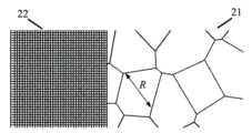
Fig. 1 is the cross sectional representation of the metal grill conductive layer based on flush type of the present invention;
Fig. 2 is the floor map of the metal grill conductive layer based on flush type of the present invention;
Fig. 3 is the enlarged drawing of K among Fig. 2;
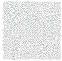
Fig. 4 is the random grid synoptic diagram of the metal grill conductive layer based on flush type of the present invention;
Fig. 5 be in the random grid of the metal grill conductive layer based on flush type of the present invention every line segment with X axle angle θ;
Fig. 6 is that the Probability p of every line segment and X axle angle distributes in the random grid of the metal grill conductive layer based on flush type of the present invention;
Fig. 7 is an alignment mark synoptic diagram of the present invention;
Fig. 8 is the enlarged drawing of L among Fig. 7.
Embodiment
To combine accompanying drawing that the specific embodiment of present technique scheme is done further to specify below.
The conductive layer in the contact conductor zone of processing with the specification mesh shape
Present embodiment is as shown in Figure 1 based on the cross sectional representation of the metal grill conductive layer of flush type.Conductive layer issubstrate PET 11 from bottom to top successively, and thickness is 188 μ m;Adhesion promoting layer 12; Esters of acrylic acid UV glue 13 with groove structure,gash depth 3 μ m, width 2.2 μ m; What fill in the groove isargent 14, and thickness is about 2 μ m less than gash depth.
Present embodiment is as shown in Figure 2 based on the floor map of the metal grill conductive layer of flush type.Conductive layer comprisestransparency electrode zone 21 and contact conductor zone 22.Transparency electrode zone 21 is made up of the irregular polygon random grid, live width 2.2 μ m, and the mean diameter R of grid all is preferably 120 μ m, and transmitance is 96% relatively.Because the PET that is selected for use in the present embodiment is 91.4% at the mean transmissivity of visible light wave range, so the whole transmitance of transparency electrode is 87.72%.Contact conductor zone 22 is by live width 2.2 μ m, and the orthogonal grid line of cycles 8 μ m constitutes, and transmitance is 53.5% relatively.
Present embodiment is as shown in Figure 2 based on the floor map of the metal grill conductive layer of flush type; 22 ' be the enlarged drawing incontact conductor zone 22 among Fig. 3 wherein, can find out that contact conductor zone 22 ' is made up of the grid of rule by enlarged drawing; The lines of black areconductive region argents 14 in the contact conductor zone 22 '; White space is an insulating regions, and the white space in the contact conductor zone 22 ' is an esters of acrylic acid UV glue 13, and the conductive material that contact conductor zone 22 ' is connected with the external world can better bonding; Key is big more with degree, and bonding is good more.
Thealignment mark 31 based on the conductive film of flush type metal grill of present embodiment is as shown in Figure 7.Alignment mark 31 also is by live width 2.2 μ m, and the orthogonal grid line of cycles 8 μ m constitutes, and transmitance is 53.5% relatively; Fig. 8 is the enlarged drawing of L among Fig. 7, can see that by Fig. 8alignment mark 31 also is to be made up of latticed.
The job operation that is adopted in the present embodiment is a prior art, and in the present embodiment, the type of random grid is an isotropy irregular polygon grid, will be the angle distribution that example is analyzed its mesh lines below with the random grid of 5mm*5mm area as shown in Figure 4.
Random grid shown in Figure 4 comprises 4257 line segments altogether.As shown in Figure 5, that adds up every line segment obtains one-dimension array θ (1) ~ θ (4257) with X axle angle θ; And then with 5oFor interval layout, with 0 ~ 180oBe divided into 36 angular interval; Drop on each interval interior Probability p in the statistics line segment, obtain one-dimension array p (1) ~ p (36), as shown in Figure 6; At last according to the standard deviation computing formula:

N is 36 in the formula, and can obtain standard deviation s is 0.26%, and average probability is 2.78%.S/=9.31% it is thus clear that the mesh lines of above-mentioned random grid is very even in angle distribution, can effectively avoid the generation of Moire fringe thus.
In the present embodiment, the random grid in irregularly shaped transparency electrode zone can also be irregular cellular structure; In practical application, out-of-shape and acyclic random grid can be to be spliced through periodicity through aperiodic random grid unit, part, and the cycle of said splicing is greater than 1 millimeter.
A kind of touch panel of the present invention possesses Fig. 1-metal grill conductive layer shown in Figure 2.Its composition mode is the GFF pattern.Promptly this touch panel possesses the two-layer metal grill conductive layer that possesses These characteristics, has OCA glue between two-layer.
Substrate in the present embodiment can also be a glass; Esters of acrylic acid UV glue described in the embodiment with groove structure; Can substitute with having the organic materials such as ultraviolet-curable materials, thermoplastic or thermosets that same nature maybe can reach identical purpose equally, for example: PMMA, PC, PDMS etc. with UV glue.This metal grill conductive layer can also be a bilateral structure, and it can also be GG that the constituted mode of touch panel does not receive limitation, on-cell, GF2 pattern etc.The structure of the conductive layer in the present embodiment can for: form by base material and conductive material at least from bottom to top; Or form by base material, polymeric material and conductive material at least from bottom to top; Or form by conductive material, base material and conductive material at least from bottom to top; Or form by conductive material, polymeric material, base material, polymeric material and conductive material at least from bottom to top.Wherein polymeric material is ultraviolet-curable materials, thermoplastic or thermosets.
More than show and described ultimate principle of the present invention and principal character and advantage of the present invention.The technician of the industry should understand; The present invention is not restricted to the described embodiments; That describes in the foregoing description and the instructions just explains principle of the present invention; Under the prerequisite that does not break away from spirit and scope of the invention, the present invention also has various changes and modifications, and these variations and improvement all fall in the scope of the invention that requires protection.The present invention requires protection domain to be defined by appending claims and equivalent thereof.
Claims (9)
1. metal grill conductive layer; This conductive layer surface comprises transparency electrode zone and contact conductor zone; Said transparency electrode zone has the grid that is made up of metal, it is characterized in that, said contact conductor zone has the grid that the conductive material by the containing metal composition constitutes; Said grid is made up of the conductive material that is filled in the containing metal composition in the groove.
2. a kind of metal grill conductive layer according to claim 1 is characterized in that, the grid in said contact conductor zone is the polygonal mesh of regular shape.
3. a kind of metal grill conductive layer according to claim 1 and 2; It is characterized in that; The grid in said transparency electrode zone is a random grid in irregular shape; The grid in said transparency electrode zone is made up of the mesh lines in transparency electrode zone, and the mesh lines in said transparency electrode zone is evenly distributed on all angles direction.
4. a kind of metal grill conductive layer according to claim 3 is characterized in that, said random grid is the grid that irregular polygon constitutes; The mesh lines of said grid is a straight-line segment, and is evenly distributed with dextrad horizontal direction X axle angulation θ, the said θ value that evenly is distributed as each bar random grid of statistics; Then according to 5oStep pitch, statistics drops on the Probability p of mesh lines in each angular intervali, thus 0 ~ 180o36 angular interval with interior obtain p1, p2To p36piSatisfy standard deviation less than 20% of arithmetic equal value.
5. a kind of metal grill conductive layer according to claim 1 and 2 is characterized in that, the relative transmitance of the grid in said contact conductor zone is less than 80%.
6. a kind of metal grill conductive layer according to claim 1 and 2 is characterized in that the xsect of said groove is approximate rectangular, and the ratio of the degree of depth of said groove and width is greater than 0.8, and said groove width is less than 10 μ m.
7. a kind of metal grill conductive layer according to claim 1 and 2 is characterized in that having alignment mark in the said conductive layer, and said alignment mark has the grid that is made up of metal, and relative transmitance is less than 80%.
8. a kind of metal grill conductive layer according to claim 1 and 2 is characterized in that the structure of this conductive layer is: be made up of base material and conductive material at least from bottom to top; Or form by base material, polymeric material and conductive material at least from bottom to top; Or form by conductive material, base material and conductive material at least from bottom to top; Or form by conductive material, polymeric material, base material, polymeric material and conductive material at least from bottom to top; Wherein polymeric material is ultraviolet-curable materials, thermoplastic or thermosets.
9. a touch panel is characterized in that: possess the described metal grill conductive layer of the arbitrary claim of a slice claim 1-8 at least.
Priority Applications (5)
| Application Number | Priority Date | Filing Date | Title |
|---|---|---|---|
| CN2012101418542ACN102722279A (en) | 2012-05-09 | 2012-05-09 | Metal grid conducting layer and touch panel equipped with the conducting layer |
| KR1020137029977AKR101537036B1 (en) | 2012-05-09 | 2012-12-20 | Metal mesh conductive layer and touch panel having the same |
| JP2014513908AJP5876928B2 (en) | 2012-05-09 | 2012-12-20 | Metal mesh conductive layer and touch panel having the same |
| PCT/CN2012/087077WO2013166840A1 (en) | 2012-05-09 | 2012-12-20 | Conductive layer of metal grid and touch panel provided with conductive layer thereof |
| US14/000,192US20140198264A1 (en) | 2012-05-09 | 2012-12-20 | Metal mesh conductive layer and touch panel having the same |
Applications Claiming Priority (1)
| Application Number | Priority Date | Filing Date | Title |
|---|---|---|---|
| CN2012101418542ACN102722279A (en) | 2012-05-09 | 2012-05-09 | Metal grid conducting layer and touch panel equipped with the conducting layer |
Publications (1)
| Publication Number | Publication Date |
|---|---|
| CN102722279Atrue CN102722279A (en) | 2012-10-10 |
Family
ID=46948072
Family Applications (1)
| Application Number | Title | Priority Date | Filing Date |
|---|---|---|---|
| CN2012101418542APendingCN102722279A (en) | 2012-05-09 | 2012-05-09 | Metal grid conducting layer and touch panel equipped with the conducting layer |
Country Status (5)
| Country | Link |
|---|---|
| US (1) | US20140198264A1 (en) |
| JP (1) | JP5876928B2 (en) |
| KR (1) | KR101537036B1 (en) |
| CN (1) | CN102722279A (en) |
| WO (1) | WO2013166840A1 (en) |
Cited By (66)
| Publication number | Priority date | Publication date | Assignee | Title |
|---|---|---|---|---|
| CN102929472A (en)* | 2012-11-27 | 2013-02-13 | 南昌欧菲光科技有限公司 | Transparent conductor for capacitive touch panel |
| CN103064576A (en)* | 2013-02-07 | 2013-04-24 | 汕头超声显示器(二厂)有限公司 | Capacitive touch screen with nano silver electrode |
| CN103079338A (en)* | 2012-12-27 | 2013-05-01 | 广东欧珀移动通信有限公司 | A kind of PCB and electronic device |
| CN103105970A (en)* | 2013-02-06 | 2013-05-15 | 南昌欧菲光科技有限公司 | Touch screen induction module and display comprising same |
| CN103106953A (en)* | 2013-02-06 | 2013-05-15 | 南昌欧菲光科技有限公司 | Conducting film and preparation method thereof and touch screen comprising the same |
| CN103105972A (en)* | 2013-02-06 | 2013-05-15 | 南昌欧菲光科技有限公司 | Touch sensitive element and touch screen comprising same |
| CN103164100A (en)* | 2013-03-28 | 2013-06-19 | 南昌欧菲光科技有限公司 | Capacitive touch screen |
| CN103165227A (en)* | 2013-03-28 | 2013-06-19 | 南昌欧菲光科技有限公司 | Transparent conductive film and connection method thereof |
| CN103176656A (en)* | 2013-03-20 | 2013-06-26 | 南昌欧菲光科技有限公司 | Touch screen and manufacturing method thereof |
| CN103176657A (en)* | 2013-03-20 | 2013-06-26 | 南昌欧菲光科技有限公司 | Touch screen and conducting layer |
| CN103176650A (en)* | 2013-03-01 | 2013-06-26 | 南昌欧菲光科技有限公司 | Conductive glass substrate and manufacturing method of conductive glass substrate |
| CN103176660A (en)* | 2013-03-28 | 2013-06-26 | 南昌欧菲光科技有限公司 | Position sensor |
| CN103197795A (en)* | 2013-03-20 | 2013-07-10 | 南昌欧菲光科技有限公司 | Conducting layer of touch screen |
| CN103236320A (en)* | 2013-03-22 | 2013-08-07 | 重庆绿色智能技术研究院 | Method for manufacturing metal grid-graphene transparent electrode and method for manufacturing touch screen from metal grid-graphene transparent electrode |
| CN103294270A (en)* | 2013-05-30 | 2013-09-11 | 南昌欧菲光科技有限公司 | Monolayer multiple-point touch conducting film and producing method thereof |
| CN103294267A (en)* | 2013-05-24 | 2013-09-11 | 苏州欧菲光科技有限公司 | Conduction structure for single-layer multi-point touch panels and single-layer multi-point touch panel |
| CN103309506A (en)* | 2013-05-30 | 2013-09-18 | 南昌欧菲光科技有限公司 | One-layer multi-point touch control conductive film and manufacturing method thereof |
| CN103336620A (en)* | 2013-07-05 | 2013-10-02 | 南昌欧菲光显示技术有限公司 | Touch display screen, optical filter component of touch display screen and preparation method of optical filter component |
| WO2013166840A1 (en)* | 2012-05-09 | 2013-11-14 | 南昌欧菲光科技有限公司 | Conductive layer of metal grid and touch panel provided with conductive layer thereof |
| CN103412669A (en)* | 2013-04-12 | 2013-11-27 | 深圳欧菲光科技股份有限公司 | Touch screen and preparation method thereof |
| CN103425320A (en)* | 2013-02-04 | 2013-12-04 | 南昌欧菲光科技有限公司 | Transparent touch screen |
| CN103425325A (en)* | 2013-03-30 | 2013-12-04 | 南昌欧菲光显示技术有限公司 | Polarizing sheet module, preparation method thereof and touch display screen |
| CN103425366A (en)* | 2013-02-04 | 2013-12-04 | 南昌欧菲光科技有限公司 | Lead electrode and preparation method thereof |
| CN103425319A (en)* | 2013-02-04 | 2013-12-04 | 南昌欧菲光科技有限公司 | Transparent touch panel |
| CN103811105A (en)* | 2012-11-09 | 2014-05-21 | 深圳欧菲光科技股份有限公司 | Transparent conductive body and preparation method thereof |
| CN103824616A (en)* | 2014-02-26 | 2014-05-28 | 南昌欧菲光科技有限公司 | Conducting film and manufacturing method thereof, touch component and touch display device |
| CN103870047A (en)* | 2012-12-07 | 2014-06-18 | 胜华科技股份有限公司 | Touch control panel |
| CN103871547A (en)* | 2014-02-26 | 2014-06-18 | 南昌欧菲光科技有限公司 | Transparent conducting film and electronic device containing same |
| CN103870075A (en)* | 2012-12-07 | 2014-06-18 | 胜华科技股份有限公司 | Capacitive touch control panel |
| CN103955310A (en)* | 2014-04-24 | 2014-07-30 | 南昌欧菲光学技术有限公司 | Screen touch tablet and full-touch electronic device provided with screen touch tablet |
| WO2014153897A1 (en)* | 2013-03-28 | 2014-10-02 | 南昌欧菲光科技有限公司 | Transparent conductive film |
| WO2014153898A1 (en)* | 2013-03-28 | 2014-10-02 | 南昌欧菲光科技有限公司 | Transparent conducting film and preparation method therefor |
| WO2014161245A1 (en)* | 2013-03-30 | 2014-10-09 | 深圳欧菲光科技股份有限公司 | Bonding finger and touchscreen |
| CN104298388A (en)* | 2013-07-17 | 2015-01-21 | 胜华科技股份有限公司 | Touch pad and method for forming grid of touch pad |
| CN104317463A (en)* | 2013-03-20 | 2015-01-28 | 南昌欧菲光科技有限公司 | Touch screen |
| CN104347153A (en)* | 2013-07-31 | 2015-02-11 | 南昌欧菲光科技有限公司 | Transparent conducting film |
| CN104347155A (en)* | 2013-07-31 | 2015-02-11 | 南昌欧菲光科技有限公司 | Transparent conducting film |
| CN104375710A (en)* | 2014-12-04 | 2015-02-25 | 合肥鑫晟光电科技有限公司 | Metal grid, touch screen and display device |
| CN104656983A (en)* | 2014-11-25 | 2015-05-27 | 业成光电(深圳)有限公司 | Touch panel and forming method for metal grid pattern |
| JP2015515709A (en)* | 2013-04-12 | 2015-05-28 | 深▲ゼン▼欧菲光科技股▲フン▼有限公司 | Touch screen sensing module, manufacturing method thereof, and display device |
| US9066427B2 (en) | 2013-03-20 | 2015-06-23 | Nanchang O-Film Tech. Co., Ltd. | Conductive layer of touch screen |
| CN104765491A (en)* | 2015-03-26 | 2015-07-08 | 业成光电(深圳)有限公司 | Manufacturing method of conductive layer of touch panel and touch panel |
| KR101556313B1 (en)* | 2013-03-08 | 2015-09-30 | 난창 오-필름 테크 컴퍼니 리미티드 | Touch panel and manufacturing method thereof |
| TWI503724B (en)* | 2013-02-06 | 2015-10-11 | Nanchang O Film Tech Co Ltd | Conductive film and manufacture method thereof and touch screen containing the conductive film |
| US9179547B2 (en) | 2013-03-30 | 2015-11-03 | Shenzhen O-Film Tech Co., Ltd. | Gold finger and touch screen |
| CN105045455A (en)* | 2015-09-07 | 2015-11-11 | 张家港康得新光电材料有限公司 | Metal grid transparent conducting film, preparation method thereof and capacitive touch screen |
| US9198285B2 (en) | 2013-03-20 | 2015-11-24 | Nanchang O-Film Tech. Co., Ltd. | Touch screen and conductive layer thereof |
| US9201551B2 (en) | 2013-03-28 | 2015-12-01 | Nanchang O-Film Tech. Co., Ltd. | Capacitive touch screen |
| CN105224122A (en)* | 2014-06-13 | 2016-01-06 | 未来奈米科技股份有限公司 | There is touch sensor and the touch panel of non-type mode sensor |
| US9268446B2 (en) | 2013-02-06 | 2016-02-23 | Nanchang O-Film Tech. Co., Ltd. | Monitor, touchscreen sensing module thereof, and method for manufacturing the touchscreen sensing module |
| US9392700B2 (en) | 2013-03-28 | 2016-07-12 | Nanchang O-Film Tech. Co., Ltd. | Transparent conductive film and preparation method thereof |
| US9510456B2 (en) | 2012-11-09 | 2016-11-29 | Shenzhen O-Film Tech Co., Ltd. | Transparent conductor and preparation method thereof |
| CN106233230A (en)* | 2014-04-15 | 2016-12-14 | 凸版印刷株式会社 | Touch sensor electrode, touch panel and display device |
| CN106775066A (en)* | 2016-11-29 | 2017-05-31 | 合肥鑫晟光电科技有限公司 | Touch-screen and preparation method thereof, touch control display apparatus |
| CN103823591B (en)* | 2014-02-26 | 2017-07-07 | 南昌欧菲光科技有限公司 | Touch control display device and its touch sensing |
| CN107066129A (en)* | 2015-09-15 | 2017-08-18 | 现代自动车株式会社 | Touch input device and its manufacture method |
| CN107077250A (en)* | 2014-09-05 | 2017-08-18 | 阿莫善斯有限公司 | Touch sensor for touch screen panel and manufacturing method thereof |
| CN107132950A (en)* | 2017-05-10 | 2017-09-05 | 昆山龙腾光电有限公司 | Contact panel and display device |
| CN107710122A (en)* | 2015-07-24 | 2018-02-16 | 富士胶片株式会社 | Grid pattern design method of conductive film for touch panel, method of manufacturing conductive film for touch panel, and conductive film for touch panel |
| CN107943356A (en)* | 2014-01-31 | 2018-04-20 | 株式会社日本显示器 | Display device and its driving method with capacitive type sensor |
| CN108292185A (en)* | 2015-11-17 | 2018-07-17 | 三菱制纸株式会社 | Transparent conductive material |
| TWI630526B (en)* | 2016-09-23 | 2018-07-21 | 大陸商蘇州維業達觸控科技有限公司 | Touch conductive film, touch module and display device |
| CN110100227A (en)* | 2016-12-20 | 2019-08-06 | 3M创新有限公司 | Grid electrode |
| CN110308828A (en)* | 2018-03-27 | 2019-10-08 | 佳冠电子股份有限公司 | Touch panel with grid pattern without sensing function |
| CN110399055A (en)* | 2019-06-27 | 2019-11-01 | 厦门理工学院 | A touch structure, preparation method and touch screen |
| CN110442265A (en)* | 2019-07-29 | 2019-11-12 | 深圳莱宝高科技股份有限公司 | Network and touch screen with it |
Families Citing this family (26)
| Publication number | Priority date | Publication date | Assignee | Title |
|---|---|---|---|---|
| US9066426B2 (en)* | 2013-03-28 | 2015-06-23 | Nanchang O-Film Tech. Co., Ltd. | Transparent conductive film |
| JP5914403B2 (en)* | 2013-03-29 | 2016-05-11 | 株式会社ジャパンディスプレイ | Display device with touch detection function and electronic device |
| US9058084B2 (en)* | 2013-04-15 | 2015-06-16 | Eastman Kodak Company | Hybrid single-side touch screen |
| KR20140129805A (en)* | 2013-04-30 | 2014-11-07 | 삼성전기주식회사 | Touch Sensor |
| KR20150009846A (en)* | 2013-07-17 | 2015-01-27 | 삼성디스플레이 주식회사 | Touch Screen Panel and Fabricating Method Thereof |
| KR20150103601A (en)* | 2014-03-03 | 2015-09-11 | 삼성전기주식회사 | Touch panel |
| JP2015195004A (en)* | 2014-03-28 | 2015-11-05 | 富士フイルム株式会社 | Conductive film and touch panel module |
| TWM505004U (en) | 2014-04-14 | 2015-07-11 | Ind Tech Res Inst | Touch panel |
| US10411078B2 (en) | 2014-04-14 | 2019-09-10 | Industrial Technology Research Institute | Sensing display apparatus |
| CN105204695B (en)* | 2014-06-12 | 2018-08-21 | 宸鸿科技(厦门)有限公司 | Nano-silver thread conductive laminate structure and capacitance type touch-control panel |
| CN104009124B (en)* | 2014-06-13 | 2018-09-18 | 苏州苏大维格光电科技股份有限公司 | The hyperfine electrode transfer film of solar cell, preparation method and applications method |
| KR102202976B1 (en) | 2014-09-19 | 2021-01-14 | 동우 화인켐 주식회사 | Touch Sensor Panel and Method for Fabricating the same |
| KR102256461B1 (en) | 2014-10-10 | 2021-05-26 | 삼성디스플레이 주식회사 | Touch sensor and display including the same |
| KR20160088530A (en) | 2015-01-15 | 2016-07-26 | 삼성디스플레이 주식회사 | Touch panel |
| WO2016136967A1 (en) | 2015-02-27 | 2016-09-01 | 株式会社フジクラ | Wiring body, wiring substrate, and touch sensor |
| KR101681745B1 (en) | 2015-03-26 | 2016-12-01 | 가천대학교 산학협력단 | Transparent electrode material |
| KR102329810B1 (en) | 2015-04-14 | 2021-11-22 | 삼성디스플레이 주식회사 | Mesh-type electrode pattern and manufacturing method thereof, and touch panel including the same |
| JP6511382B2 (en) | 2015-10-16 | 2019-05-15 | 富士フイルム株式会社 | CONDUCTIVE FILM AND DISPLAY DEVICE PROVIDED WITH THE SAME |
| JP2019517053A (en)* | 2016-04-05 | 2019-06-20 | スリーエム イノベイティブ プロパティズ カンパニー | Nanowire contact pad with improved adhesion to metal interconnects |
| WO2020222627A1 (en)* | 2019-04-29 | 2020-11-05 | 주식회사 아모그린텍 | Touch screen panel and manufacturing method thereof |
| US12133327B2 (en) | 2019-05-06 | 2024-10-29 | 3M Innovative Properties Company | Patterned article including electrically conductive elements |
| CN114096915A (en) | 2019-07-16 | 2022-02-25 | 爱克发-格法特公司 | Method of manufacturing transparent conductive film |
| CN111009339A (en)* | 2019-12-24 | 2020-04-14 | 江西蓝沛泰和新材料有限公司 | Conductive structure and preparation method thereof, touch panel and display device |
| KR102822260B1 (en)* | 2019-12-31 | 2025-06-18 | 미래나노텍(주) | Screen apparatus |
| EP4105830A4 (en) | 2020-02-13 | 2023-07-19 | Asahi Kasei Kabushiki Kaisha | Transparent antenna and rf tag |
| KR102766427B1 (en)* | 2020-08-28 | 2025-02-12 | 동우 화인켐 주식회사 | Conductive mesh structure and antenna device including the same |
Citations (8)
| Publication number | Priority date | Publication date | Assignee | Title |
|---|---|---|---|---|
| US20090218651A1 (en)* | 2008-02-28 | 2009-09-03 | Sunlight Photonics Inc. | Composite substrates for thin film electro-optical devices |
| JP2010182137A (en)* | 2009-02-06 | 2010-08-19 | Sony Corp | Touch panel and method for manufacturing the same |
| JP2010191504A (en)* | 2009-02-16 | 2010-09-02 | Gunze Ltd | Touch switch |
| KR20110007593A (en)* | 2009-07-16 | 2011-01-24 | 주식회사 엘지화학 | Conductor and manufacturing method thereof |
| CN102067245A (en)* | 2008-07-04 | 2011-05-18 | 户田工业株式会社 | Transparent electrically conductive transfer plate and production method therefor, transparent electrically conductive base, method for producing transparent electrically conductive base using transparent electrically conductive transfer plate, and molded product using the transparent conductive substrate |
| CN102129320A (en)* | 2010-12-31 | 2011-07-20 | 友达光电股份有限公司 | Touch panel manufacturing method and touch panel |
| CN102222538A (en)* | 2011-03-11 | 2011-10-19 | 苏州纳格光电科技有限公司 | Graphical flexible transparent conductive film and preparation method thereof |
| TW201203064A (en)* | 2010-03-03 | 2012-01-16 | Miraenanotech Co Ltd | A capacitive touch panel and a method for manufacturing the same |
Family Cites Families (22)
| Publication number | Priority date | Publication date | Assignee | Title |
|---|---|---|---|---|
| WO2009085224A2 (en)* | 2007-12-20 | 2009-07-09 | Cima Nanotech Israel Ltd. | Photovoltaic device having transparent electrode formed with nanoparticles |
| CN102017071B (en)* | 2008-02-28 | 2013-12-18 | 3M创新有限公司 | Method of patterning a conductor on a substrate |
| KR101720919B1 (en)* | 2008-02-28 | 2017-03-28 | 쓰리엠 이노베이티브 프로퍼티즈 컴파니 | Touch screen sensor |
| KR100939223B1 (en)* | 2008-03-06 | 2010-01-28 | 미래나노텍(주) | Electromagnetic shielding film, front filter using the same and manufacturing method thereof |
| TWI373665B (en)* | 2008-12-25 | 2012-10-01 | Au Optronics Corp | Touch panel structure |
| WO2010090487A2 (en)* | 2009-02-06 | 2010-08-12 | 주식회사 엘지화학 | Touch screen and manufacturing method thereof |
| KR100909265B1 (en)* | 2009-02-23 | 2009-07-27 | (주)이엔에이치테크 | Manufacturing method of capacitive touch screen panel |
| JP2010251230A (en)* | 2009-04-20 | 2010-11-04 | Fujifilm Corp | Electric window glass |
| JP2012014669A (en)* | 2009-11-20 | 2012-01-19 | Fujifilm Corp | Conductive sheet, method of using conductive sheet and electrostatic capacitive touch panel |
| KR101728818B1 (en)* | 2010-08-09 | 2017-04-21 | 미래나노텍(주) | Electrostatic capacity type touch panel and manufacturing method thereof |
| JP5398623B2 (en)* | 2010-03-31 | 2014-01-29 | 富士フイルム株式会社 | Method for producing transparent conductive film, conductive film and program |
| JP5620193B2 (en)* | 2010-08-23 | 2014-11-05 | 株式会社ジャパンディスプレイ | Display device with touch detection function, touch detection device, and electronic device |
| KR101153389B1 (en)* | 2010-09-27 | 2012-06-07 | 엘지이노텍 주식회사 | Touch screen panel and touch screen assembly including the same |
| WO2012053498A1 (en)* | 2010-10-18 | 2012-04-26 | グンゼ株式会社 | Touch switch |
| WO2012106424A2 (en)* | 2011-02-02 | 2012-08-09 | 3M Innovative Properties Company | Patterned substrates with darkened mutlilayered conductor traces |
| CN102279684B (en)* | 2011-08-30 | 2014-02-12 | 深圳市豪威薄膜技术有限公司 | Novel electrode lead capacitive screen manufacturing method and its product and touch screen terminal |
| JP5777251B2 (en)* | 2011-12-16 | 2015-09-09 | 富士フイルム株式会社 | Conductive sheet for touch panel and touch panel |
| JP5748647B2 (en)* | 2011-12-22 | 2015-07-15 | 富士フイルム株式会社 | Conductive sheet and touch panel |
| JP5509186B2 (en)* | 2011-12-16 | 2014-06-04 | 富士フイルム株式会社 | Touch panel and conductive sheet for touch panel |
| JP5822395B2 (en)* | 2012-01-25 | 2015-11-24 | 富士フイルム株式会社 | Conductive sheet, inspection method and manufacturing method thereof |
| CN102722279A (en)* | 2012-05-09 | 2012-10-10 | 崔铮 | Metal grid conducting layer and touch panel equipped with the conducting layer |
| CN202584074U (en)* | 2012-05-09 | 2012-12-05 | 崔铮 | Metal grid conducting layer and touch panel with same |
- 2012
- 2012-05-09CNCN2012101418542Apatent/CN102722279A/enactivePending
- 2012-12-20JPJP2014513908Apatent/JP5876928B2/ennot_activeExpired - Fee Related
- 2012-12-20WOPCT/CN2012/087077patent/WO2013166840A1/enactiveApplication Filing
- 2012-12-20KRKR1020137029977Apatent/KR101537036B1/ennot_activeExpired - Fee Related
- 2012-12-20USUS14/000,192patent/US20140198264A1/ennot_activeAbandoned
Patent Citations (8)
| Publication number | Priority date | Publication date | Assignee | Title |
|---|---|---|---|---|
| US20090218651A1 (en)* | 2008-02-28 | 2009-09-03 | Sunlight Photonics Inc. | Composite substrates for thin film electro-optical devices |
| CN102067245A (en)* | 2008-07-04 | 2011-05-18 | 户田工业株式会社 | Transparent electrically conductive transfer plate and production method therefor, transparent electrically conductive base, method for producing transparent electrically conductive base using transparent electrically conductive transfer plate, and molded product using the transparent conductive substrate |
| JP2010182137A (en)* | 2009-02-06 | 2010-08-19 | Sony Corp | Touch panel and method for manufacturing the same |
| JP2010191504A (en)* | 2009-02-16 | 2010-09-02 | Gunze Ltd | Touch switch |
| KR20110007593A (en)* | 2009-07-16 | 2011-01-24 | 주식회사 엘지화학 | Conductor and manufacturing method thereof |
| TW201203064A (en)* | 2010-03-03 | 2012-01-16 | Miraenanotech Co Ltd | A capacitive touch panel and a method for manufacturing the same |
| CN102129320A (en)* | 2010-12-31 | 2011-07-20 | 友达光电股份有限公司 | Touch panel manufacturing method and touch panel |
| CN102222538A (en)* | 2011-03-11 | 2011-10-19 | 苏州纳格光电科技有限公司 | Graphical flexible transparent conductive film and preparation method thereof |
Cited By (108)
| Publication number | Priority date | Publication date | Assignee | Title |
|---|---|---|---|---|
| WO2013166840A1 (en)* | 2012-05-09 | 2013-11-14 | 南昌欧菲光科技有限公司 | Conductive layer of metal grid and touch panel provided with conductive layer thereof |
| US9510456B2 (en) | 2012-11-09 | 2016-11-29 | Shenzhen O-Film Tech Co., Ltd. | Transparent conductor and preparation method thereof |
| CN103811105B (en)* | 2012-11-09 | 2016-11-16 | 深圳欧菲光科技股份有限公司 | Transparent conductor and preparation method thereof |
| CN103811105A (en)* | 2012-11-09 | 2014-05-21 | 深圳欧菲光科技股份有限公司 | Transparent conductive body and preparation method thereof |
| CN102929472A (en)* | 2012-11-27 | 2013-02-13 | 南昌欧菲光科技有限公司 | Transparent conductor for capacitive touch panel |
| CN103870075A (en)* | 2012-12-07 | 2014-06-18 | 胜华科技股份有限公司 | Capacitive touch control panel |
| CN103870047A (en)* | 2012-12-07 | 2014-06-18 | 胜华科技股份有限公司 | Touch control panel |
| CN103079338A (en)* | 2012-12-27 | 2013-05-01 | 广东欧珀移动通信有限公司 | A kind of PCB and electronic device |
| CN103425319B (en)* | 2013-02-04 | 2016-08-24 | 南昌欧菲光科技有限公司 | Transparent touch-control panel |
| CN103425320A (en)* | 2013-02-04 | 2013-12-04 | 南昌欧菲光科技有限公司 | Transparent touch screen |
| WO2014117478A1 (en)* | 2013-02-04 | 2014-08-07 | 南昌欧菲光科技有限公司 | Lead electrode and preparation method therefor |
| JP2015508550A (en)* | 2013-02-04 | 2015-03-19 | 南昌欧菲光科技有限公司Nanchang O−Film Tech. Co., Ltd. | Lead electrode and manufacturing method thereof |
| KR101558724B1 (en)* | 2013-02-04 | 2015-10-07 | 난창 오-필름 테크 컴퍼니 리미티드 | Lead electrode and preparation method thereof |
| CN103425319A (en)* | 2013-02-04 | 2013-12-04 | 南昌欧菲光科技有限公司 | Transparent touch panel |
| TWI553813B (en)* | 2013-02-04 | 2016-10-11 | 南昌歐菲光科技有限公司 | Lead electrode and preparation method thereof |
| CN103425366A (en)* | 2013-02-04 | 2013-12-04 | 南昌欧菲光科技有限公司 | Lead electrode and preparation method thereof |
| CN103425366B (en)* | 2013-02-04 | 2016-08-03 | 南昌欧菲光科技有限公司 | Lead-in wire electrode and preparation method thereof |
| TWI503724B (en)* | 2013-02-06 | 2015-10-11 | Nanchang O Film Tech Co Ltd | Conductive film and manufacture method thereof and touch screen containing the conductive film |
| CN103105972A (en)* | 2013-02-06 | 2013-05-15 | 南昌欧菲光科技有限公司 | Touch sensitive element and touch screen comprising same |
| TWI503715B (en)* | 2013-02-06 | 2015-10-11 | Nanchang O Film Tech Co Ltd | Conductive film and manufacture method thereof and touch screen containing the conductive film |
| US9313887B2 (en) | 2013-02-06 | 2016-04-12 | Nanchang O-Film Tech. Co., Ltd. | Conductive film, manufacturing method thereof, and touch screen having the same |
| CN103106953B (en)* | 2013-02-06 | 2014-11-26 | 南昌欧菲光科技有限公司 | Conducting film and preparation method thereof and touch screen comprising the same |
| CN103106953A (en)* | 2013-02-06 | 2013-05-15 | 南昌欧菲光科技有限公司 | Conducting film and preparation method thereof and touch screen comprising the same |
| CN103105970A (en)* | 2013-02-06 | 2013-05-15 | 南昌欧菲光科技有限公司 | Touch screen induction module and display comprising same |
| US9268446B2 (en) | 2013-02-06 | 2016-02-23 | Nanchang O-Film Tech. Co., Ltd. | Monitor, touchscreen sensing module thereof, and method for manufacturing the touchscreen sensing module |
| CN103105970B (en)* | 2013-02-06 | 2014-09-17 | 南昌欧菲光科技有限公司 | Touch screen induction module and display comprising same |
| KR101554573B1 (en) | 2013-02-06 | 2015-09-21 | 난창 오-필름 테크 컴퍼니 리미티드 | Conductive film, manufacturing method thereof, and touch screen including the conducting film |
| TWI493409B (en)* | 2013-02-06 | 2015-07-21 | 南昌歐菲光科技有限公司 | Displayer and touch screen inductive module thereof |
| CN103064576A (en)* | 2013-02-07 | 2013-04-24 | 汕头超声显示器(二厂)有限公司 | Capacitive touch screen with nano silver electrode |
| CN103064576B (en)* | 2013-02-07 | 2015-08-05 | 汕头超声显示器(二厂)有限公司 | A kind of capacitance touch screen with nano silver electrode |
| US9089081B2 (en) | 2013-03-01 | 2015-07-21 | Nanchang O-Film Tech. Co., Ltd. | Conductive glass substrate and preparation method thereof |
| CN103176650A (en)* | 2013-03-01 | 2013-06-26 | 南昌欧菲光科技有限公司 | Conductive glass substrate and manufacturing method of conductive glass substrate |
| KR101556313B1 (en)* | 2013-03-08 | 2015-09-30 | 난창 오-필름 테크 컴퍼니 리미티드 | Touch panel and manufacturing method thereof |
| WO2014146382A1 (en)* | 2013-03-20 | 2014-09-25 | 南昌欧菲光科技有限公司 | Touch screen and manufacturing method therefor |
| CN103176657B (en)* | 2013-03-20 | 2015-11-25 | 南昌欧菲光科技有限公司 | Touch-screen and conductive layer thereof |
| WO2014146384A1 (en)* | 2013-03-20 | 2014-09-25 | 南昌欧菲光科技有限公司 | Touch screen and electrically-conductive layer thereof |
| KR101543594B1 (en) | 2013-03-20 | 2015-08-11 | 난창 오-필름 테크 컴퍼니 리미티드 | Touch screen and conductive layer thereof |
| US9198285B2 (en) | 2013-03-20 | 2015-11-24 | Nanchang O-Film Tech. Co., Ltd. | Touch screen and conductive layer thereof |
| TWI494815B (en)* | 2013-03-20 | 2015-08-01 | Nanchang O Film Tech Co Ltd | Touch panel and producing method thereof |
| TWI494817B (en)* | 2013-03-20 | 2015-08-01 | Nanchang O Film Tech Co Ltd | Conductive layer of touch panel |
| TWI494816B (en)* | 2013-03-20 | 2015-08-01 | Nanchang O Film Tech Co Ltd | Touch panel and conductive layer of the same |
| CN103176657A (en)* | 2013-03-20 | 2013-06-26 | 南昌欧菲光科技有限公司 | Touch screen and conducting layer |
| US9066427B2 (en) | 2013-03-20 | 2015-06-23 | Nanchang O-Film Tech. Co., Ltd. | Conductive layer of touch screen |
| CN104317463A (en)* | 2013-03-20 | 2015-01-28 | 南昌欧菲光科技有限公司 | Touch screen |
| US9063604B2 (en) | 2013-03-20 | 2015-06-23 | Nanchang O-Film Tech. Co., Ltd. | Touch screen and manufacturing method thereof |
| CN103176656A (en)* | 2013-03-20 | 2013-06-26 | 南昌欧菲光科技有限公司 | Touch screen and manufacturing method thereof |
| CN103197795A (en)* | 2013-03-20 | 2013-07-10 | 南昌欧菲光科技有限公司 | Conducting layer of touch screen |
| CN103176656B (en)* | 2013-03-20 | 2015-05-13 | 南昌欧菲光科技有限公司 | Touch screen and manufacturing method thereof |
| CN103197795B (en)* | 2013-03-20 | 2015-04-08 | 南昌欧菲光科技有限公司 | Conducting layer of touch screen |
| CN103236320A (en)* | 2013-03-22 | 2013-08-07 | 重庆绿色智能技术研究院 | Method for manufacturing metal grid-graphene transparent electrode and method for manufacturing touch screen from metal grid-graphene transparent electrode |
| KR20140005627U (en)* | 2013-03-28 | 2014-10-31 | 난창 오-필름 테크 컴퍼니 리미티드 | Transparent Conductive Film |
| WO2014153897A1 (en)* | 2013-03-28 | 2014-10-02 | 南昌欧菲光科技有限公司 | Transparent conductive film |
| US9392700B2 (en) | 2013-03-28 | 2016-07-12 | Nanchang O-Film Tech. Co., Ltd. | Transparent conductive film and preparation method thereof |
| CN103164100B (en)* | 2013-03-28 | 2014-08-06 | 南昌欧菲光科技有限公司 | Capacitive touch screen |
| KR200482910Y1 (en) | 2013-03-28 | 2017-03-14 | 난창 오-필름 테크 컴퍼니 리미티드 | Transparent conductive film |
| CN103176660A (en)* | 2013-03-28 | 2013-06-26 | 南昌欧菲光科技有限公司 | Position sensor |
| KR101584798B1 (en) | 2013-03-28 | 2016-01-12 | 난창 오-필름 테크 컴퍼니 리미티드 | TRANSPARENT Conductive FILM and PREPARATION METHOD THEREOF |
| US9201551B2 (en) | 2013-03-28 | 2015-12-01 | Nanchang O-Film Tech. Co., Ltd. | Capacitive touch screen |
| JP2015513755A (en)* | 2013-03-28 | 2015-05-14 | ナンチャン オー−フィルム テック カンパニー リミテッド | Capacitive touch screen |
| CN103165227A (en)* | 2013-03-28 | 2013-06-19 | 南昌欧菲光科技有限公司 | Transparent conductive film and connection method thereof |
| CN103176660B (en)* | 2013-03-28 | 2015-09-30 | 南昌欧菲光科技有限公司 | Position transducer |
| WO2014153899A1 (en)* | 2013-03-28 | 2014-10-02 | 南昌欧菲光科技有限公司 | Capacitive touchscreen |
| WO2014153898A1 (en)* | 2013-03-28 | 2014-10-02 | 南昌欧菲光科技有限公司 | Transparent conducting film and preparation method therefor |
| CN103165227B (en)* | 2013-03-28 | 2014-09-17 | 南昌欧菲光科技有限公司 | Transparent conductive film and connection method thereof |
| CN103164100A (en)* | 2013-03-28 | 2013-06-19 | 南昌欧菲光科技有限公司 | Capacitive touch screen |
| CN103425325B (en)* | 2013-03-30 | 2016-12-28 | 南昌欧菲光显示技术有限公司 | Polaroid module and preparation method thereof and touch display screen |
| US9179547B2 (en) | 2013-03-30 | 2015-11-03 | Shenzhen O-Film Tech Co., Ltd. | Gold finger and touch screen |
| WO2014161245A1 (en)* | 2013-03-30 | 2014-10-09 | 深圳欧菲光科技股份有限公司 | Bonding finger and touchscreen |
| CN103425325A (en)* | 2013-03-30 | 2013-12-04 | 南昌欧菲光显示技术有限公司 | Polarizing sheet module, preparation method thereof and touch display screen |
| CN103412669A (en)* | 2013-04-12 | 2013-11-27 | 深圳欧菲光科技股份有限公司 | Touch screen and preparation method thereof |
| JP2015515709A (en)* | 2013-04-12 | 2015-05-28 | 深▲ゼン▼欧菲光科技股▲フン▼有限公司 | Touch screen sensing module, manufacturing method thereof, and display device |
| CN103412669B (en)* | 2013-04-12 | 2015-04-08 | 深圳欧菲光科技股份有限公司 | Touch screen and preparation method thereof |
| CN103294267A (en)* | 2013-05-24 | 2013-09-11 | 苏州欧菲光科技有限公司 | Conduction structure for single-layer multi-point touch panels and single-layer multi-point touch panel |
| CN103294270A (en)* | 2013-05-30 | 2013-09-11 | 南昌欧菲光科技有限公司 | Monolayer multiple-point touch conducting film and producing method thereof |
| CN103309506A (en)* | 2013-05-30 | 2013-09-18 | 南昌欧菲光科技有限公司 | One-layer multi-point touch control conductive film and manufacturing method thereof |
| CN103336620A (en)* | 2013-07-05 | 2013-10-02 | 南昌欧菲光显示技术有限公司 | Touch display screen, optical filter component of touch display screen and preparation method of optical filter component |
| CN104298388A (en)* | 2013-07-17 | 2015-01-21 | 胜华科技股份有限公司 | Touch pad and method for forming grid of touch pad |
| CN104347153A (en)* | 2013-07-31 | 2015-02-11 | 南昌欧菲光科技有限公司 | Transparent conducting film |
| CN104347155A (en)* | 2013-07-31 | 2015-02-11 | 南昌欧菲光科技有限公司 | Transparent conducting film |
| CN107943356A (en)* | 2014-01-31 | 2018-04-20 | 株式会社日本显示器 | Display device and its driving method with capacitive type sensor |
| CN107943356B (en)* | 2014-01-31 | 2021-10-26 | 株式会社日本显示器 | Display device with capacitance type sensor and method of driving the same |
| CN103824616A (en)* | 2014-02-26 | 2014-05-28 | 南昌欧菲光科技有限公司 | Conducting film and manufacturing method thereof, touch component and touch display device |
| CN103823591B (en)* | 2014-02-26 | 2017-07-07 | 南昌欧菲光科技有限公司 | Touch control display device and its touch sensing |
| CN103871547A (en)* | 2014-02-26 | 2014-06-18 | 南昌欧菲光科技有限公司 | Transparent conducting film and electronic device containing same |
| CN103824616B (en)* | 2014-02-26 | 2017-01-11 | 南昌欧菲光科技有限公司 | Conducting film and manufacturing method thereof, touch component and touch display device |
| CN106233230A (en)* | 2014-04-15 | 2016-12-14 | 凸版印刷株式会社 | Touch sensor electrode, touch panel and display device |
| CN103955310A (en)* | 2014-04-24 | 2014-07-30 | 南昌欧菲光学技术有限公司 | Screen touch tablet and full-touch electronic device provided with screen touch tablet |
| CN105224122A (en)* | 2014-06-13 | 2016-01-06 | 未来奈米科技股份有限公司 | There is touch sensor and the touch panel of non-type mode sensor |
| CN107077250A (en)* | 2014-09-05 | 2017-08-18 | 阿莫善斯有限公司 | Touch sensor for touch screen panel and manufacturing method thereof |
| CN104656983A (en)* | 2014-11-25 | 2015-05-27 | 业成光电(深圳)有限公司 | Touch panel and forming method for metal grid pattern |
| CN104375710B (en)* | 2014-12-04 | 2018-01-09 | 合肥鑫晟光电科技有限公司 | A kind of metal grill, touch-screen and display device |
| CN104375710A (en)* | 2014-12-04 | 2015-02-25 | 合肥鑫晟光电科技有限公司 | Metal grid, touch screen and display device |
| US10156924B2 (en) | 2014-12-04 | 2018-12-18 | Boe Technology Group Co., Ltd. | Metal grid, touch screen display device and a manufacture method for touch screen |
| CN104765491A (en)* | 2015-03-26 | 2015-07-08 | 业成光电(深圳)有限公司 | Manufacturing method of conductive layer of touch panel and touch panel |
| CN107710122B (en)* | 2015-07-24 | 2020-09-11 | 富士胶片株式会社 | Grid pattern design method of conductive film for touch panel, method for producing conductive film for touch panel, and conductive film for touch panel |
| CN107710122A (en)* | 2015-07-24 | 2018-02-16 | 富士胶片株式会社 | Grid pattern design method of conductive film for touch panel, method of manufacturing conductive film for touch panel, and conductive film for touch panel |
| CN105045455A (en)* | 2015-09-07 | 2015-11-11 | 张家港康得新光电材料有限公司 | Metal grid transparent conducting film, preparation method thereof and capacitive touch screen |
| CN107066129A (en)* | 2015-09-15 | 2017-08-18 | 现代自动车株式会社 | Touch input device and its manufacture method |
| CN108292185A (en)* | 2015-11-17 | 2018-07-17 | 三菱制纸株式会社 | Transparent conductive material |
| CN108292185B (en)* | 2015-11-17 | 2021-05-28 | 三菱制纸株式会社 | Translucent conductive material |
| TWI630526B (en)* | 2016-09-23 | 2018-07-21 | 大陸商蘇州維業達觸控科技有限公司 | Touch conductive film, touch module and display device |
| CN106775066A (en)* | 2016-11-29 | 2017-05-31 | 合肥鑫晟光电科技有限公司 | Touch-screen and preparation method thereof, touch control display apparatus |
| CN106775066B (en)* | 2016-11-29 | 2024-04-05 | 合肥鑫晟光电科技有限公司 | Touch screen and manufacturing method thereof, touch display device |
| CN110100227A (en)* | 2016-12-20 | 2019-08-06 | 3M创新有限公司 | Grid electrode |
| CN107132950A (en)* | 2017-05-10 | 2017-09-05 | 昆山龙腾光电有限公司 | Contact panel and display device |
| CN110308828A (en)* | 2018-03-27 | 2019-10-08 | 佳冠电子股份有限公司 | Touch panel with grid pattern without sensing function |
| CN110399055A (en)* | 2019-06-27 | 2019-11-01 | 厦门理工学院 | A touch structure, preparation method and touch screen |
| CN110442265A (en)* | 2019-07-29 | 2019-11-12 | 深圳莱宝高科技股份有限公司 | Network and touch screen with it |
Also Published As
| Publication number | Publication date |
|---|---|
| US20140198264A1 (en) | 2014-07-17 |
| JP2014519129A (en) | 2014-08-07 |
| KR20140010980A (en) | 2014-01-27 |
| KR101537036B1 (en) | 2015-07-15 |
| JP5876928B2 (en) | 2016-03-02 |
| WO2013166840A1 (en) | 2013-11-14 |
Similar Documents
| Publication | Publication Date | Title |
|---|---|---|
| CN102722279A (en) | Metal grid conducting layer and touch panel equipped with the conducting layer | |
| US10959335B2 (en) | Method for manufacturing a transparent conductive film | |
| US20140116754A1 (en) | Conductive structure of transparent conductive film, transparent conductive film and preparation method thereof | |
| TWI540599B (en) | Conductive film and preparation method thereof, touch panel using the same | |
| CN202584074U (en) | Metal grid conducting layer and touch panel with same | |
| KR200479733Y1 (en) | Polarizer module, method of manufacturing the same and touch screen using the same | |
| TWM485451U (en) | Filter module and touch screen having the same | |
| CN203422722U (en) | Narrow-frame touch screen | |
| CN203250547U (en) | Transparent conductive film | |
| CN103165227A (en) | Transparent conductive film and connection method thereof | |
| CN103413593A (en) | Transparent electric conductor and preparation method thereof | |
| KR20140141469A (en) | Touch-screen conductive film and manufacturing method thereof | |
| US20140290984A1 (en) | Transparent conductive film | |
| CN103440065B (en) | Touch control component | |
| CN104375735B (en) | Contact panel and display device | |
| CN203376990U (en) | Transparent conductive film | |
| CN104345937B (en) | Narrow bezel touch screen | |
| CN203038679U (en) | Conductive structure in transparent conductive film and transparent conductive film | |
| CN203178966U (en) | Touch display screen and optical filter module of touch display screen | |
| CN203179570U (en) | Transparent conductive film | |
| CN103425324B (en) | Polarisation filtration module and touch display screen | |
| CN203178967U (en) | Polarizer module and touch display screen | |
| CN204215395U (en) | Contact panel and display device | |
| CN203178968U (en) | Polarized light filtering module and touch display screen | |
| CN203376712U (en) | Touch screen element and touch screen |
Legal Events
| Date | Code | Title | Description |
|---|---|---|---|
| C06 | Publication | ||
| PB01 | Publication | ||
| C10 | Entry into substantive examination | ||
| SE01 | Entry into force of request for substantive examination | ||
| ASS | Succession or assignment of patent right | Owner name:NANCHANG O-FILM TECH. CO., LTD. Free format text:FORMER OWNER: CUI ZHENG Effective date:20121130 | |
| C41 | Transfer of patent application or patent right or utility model | ||
| COR | Change of bibliographic data | Free format text:CORRECT: ADDRESS; TO: 330026 NANCHANG, JIANGXI PROVINCE | |
| TA01 | Transfer of patent application right | Effective date of registration:20121130 Address after:Huangjiahu road 330026 Jiangxi Nanchang economic and Technological Development Zone Applicant after:Nanchang OFilm Tech. Co.,Ltd. Address before:A Bindon Mons, Oxford, England 17 Applicant before:Cui Zheng | |
| C12 | Rejection of a patent application after its publication | ||
| RJ01 | Rejection of invention patent application after publication | Application publication date:20121010 |