CN102709269A - 3D Array Memory Device with Improved Uniformity of Bit Line Capacitance - Google Patents
3D Array Memory Device with Improved Uniformity of Bit Line CapacitanceDownload PDFInfo
- Publication number
- CN102709269A CN102709269ACN2011103440955ACN201110344095ACN102709269ACN 102709269 ACN102709269 ACN 102709269ACN 2011103440955 ACN2011103440955 ACN 2011103440955ACN 201110344095 ACN201110344095 ACN 201110344095ACN 102709269 ACN102709269 ACN 102709269A
- Authority
- CN
- China
- Prior art keywords
- memory
- array
- semiconductor
- bit line
- strips
- Prior art date
- Legal status (The legal status is an assumption and is not a legal conclusion. Google has not performed a legal analysis and makes no representation as to the accuracy of the status listed.)
- Granted
Links
- 230000015654memoryEffects0.000claimsabstractdescription244
- 239000004065semiconductorSubstances0.000claimsdescription212
- 239000000463materialSubstances0.000claimsdescription99
- 230000005641tunnelingEffects0.000claimsdescription28
- 239000011810insulating materialSubstances0.000claimsdescription14
- 230000000903blocking effectEffects0.000claimsdescription12
- 239000000758substrateSubstances0.000claimsdescription11
- 230000008878couplingEffects0.000abstractdescription3
- 238000010168coupling processMethods0.000abstractdescription3
- 238000005859coupling reactionMethods0.000abstractdescription3
- 239000010410layerSubstances0.000description182
- 210000004027cellAnatomy0.000description105
- VYPSYNLAJGMNEJ-UHFFFAOYSA-NSilicium dioxideChemical compoundO=[Si]=OVYPSYNLAJGMNEJ-UHFFFAOYSA-N0.000description41
- 238000010586diagramMethods0.000description27
- 238000000034methodMethods0.000description27
- 230000008569processEffects0.000description22
- 229910052751metalInorganic materials0.000description21
- 239000002184metalSubstances0.000description21
- 229910021420polycrystalline siliconInorganic materials0.000description21
- 229920005591polysiliconPolymers0.000description21
- 239000000377silicon dioxideSubstances0.000description21
- 108091006146ChannelsProteins0.000description20
- 235000012239silicon dioxideNutrition0.000description19
- 229910052581Si3N4Inorganic materials0.000description14
- HQVNEWCFYHHQES-UHFFFAOYSA-Nsilicon nitrideChemical compoundN12[Si]34N5[Si]62N3[Si]51N64HQVNEWCFYHHQES-UHFFFAOYSA-N0.000description14
- 238000013461designMethods0.000description11
- 238000005516engineering processMethods0.000description11
- 238000000151depositionMethods0.000description8
- 229910021332silicideInorganic materials0.000description8
- FVBUAEGBCNSCDD-UHFFFAOYSA-Nsilicide(4-)Chemical compound[Si-4]FVBUAEGBCNSCDD-UHFFFAOYSA-N0.000description8
- 229910052710siliconInorganic materials0.000description8
- 239000010703siliconSubstances0.000description8
- 238000003860storageMethods0.000description8
- 230000008021depositionEffects0.000description7
- 230000005684electric fieldEffects0.000description7
- 238000004518low pressure chemical vapour depositionMethods0.000description7
- XUIMIQQOPSSXEZ-UHFFFAOYSA-NSiliconChemical compound[Si]XUIMIQQOPSSXEZ-UHFFFAOYSA-N0.000description6
- 230000005669field effectEffects0.000description5
- 239000007943implantSubstances0.000description5
- 238000002955isolationMethods0.000description5
- 238000001459lithographyMethods0.000description5
- 238000004519manufacturing processMethods0.000description5
- 238000003491arrayMethods0.000description4
- 239000002131composite materialSubstances0.000description4
- 229910021421monocrystalline siliconInorganic materials0.000description4
- 239000002070nanowireSubstances0.000description4
- 230000004888barrier functionEffects0.000description3
- 230000015572biosynthetic processEffects0.000description3
- 239000002071nanotubeSubstances0.000description3
- 150000004767nitridesChemical class0.000description3
- 230000003647oxidationEffects0.000description3
- 238000007254oxidation reactionMethods0.000description3
- 239000007787solidSubstances0.000description3
- 239000010409thin filmSubstances0.000description3
- QGZKDVFQNNGYKY-UHFFFAOYSA-NAmmoniaChemical compoundNQGZKDVFQNNGYKY-UHFFFAOYSA-N0.000description2
- MWUXSHHQAYIFBG-UHFFFAOYSA-NNitric oxideChemical compoundO=[N]MWUXSHHQAYIFBG-UHFFFAOYSA-N0.000description2
- GQPLMRYTRLFLPF-UHFFFAOYSA-NNitrous OxideChemical compound[O-][N+]#NGQPLMRYTRLFLPF-UHFFFAOYSA-N0.000description2
- 230000008901benefitEffects0.000description2
- 229910017052cobaltInorganic materials0.000description2
- 239000010941cobaltSubstances0.000description2
- GUTLYIVDDKVIGB-UHFFFAOYSA-Ncobalt atomChemical compound[Co]GUTLYIVDDKVIGB-UHFFFAOYSA-N0.000description2
- 238000004590computer programMethods0.000description2
- 239000004020conductorSubstances0.000description2
- 239000013078crystalSubstances0.000description2
- 230000007423decreaseEffects0.000description2
- MROCJMGDEKINLD-UHFFFAOYSA-NdichlorosilaneChemical compoundCl[SiH2]ClMROCJMGDEKINLD-UHFFFAOYSA-N0.000description2
- 238000005530etchingMethods0.000description2
- 230000006870functionEffects0.000description2
- 238000007689inspectionMethods0.000description2
- 238000012986modificationMethods0.000description2
- 230000004048modificationEffects0.000description2
- 239000002243precursorSubstances0.000description2
- 238000007493shaping processMethods0.000description2
- LIVNPJMFVYWSIS-UHFFFAOYSA-Nsilicon monoxideChemical class[Si-]#[O+]LIVNPJMFVYWSIS-UHFFFAOYSA-N0.000description2
- 229910052814silicon oxideInorganic materials0.000description2
- 229910021341titanium silicideInorganic materials0.000description2
- WFKWXMTUELFFGS-UHFFFAOYSA-NtungstenChemical compound[W]WFKWXMTUELFFGS-UHFFFAOYSA-N0.000description2
- 229910052721tungstenInorganic materials0.000description2
- 239000010937tungstenSubstances0.000description2
- WQJQOUPTWCFRMM-UHFFFAOYSA-Ntungsten disilicideChemical compound[Si]#[W]#[Si]WQJQOUPTWCFRMM-UHFFFAOYSA-N0.000description2
- 229910021342tungsten silicideInorganic materials0.000description2
- 238000012935AveragingMethods0.000description1
- OKTJSMMVPCPJKN-UHFFFAOYSA-NCarbonChemical compound[C]OKTJSMMVPCPJKN-UHFFFAOYSA-N0.000description1
- 108010075750P-Type Calcium ChannelsProteins0.000description1
- 229910021529ammoniaInorganic materials0.000description1
- 238000013459approachMethods0.000description1
- 230000009286beneficial effectEffects0.000description1
- 230000005540biological transmissionEffects0.000description1
- 229910052799carbonInorganic materials0.000description1
- 238000006243chemical reactionMethods0.000description1
- 229910052681coesiteInorganic materials0.000description1
- 229910052906cristobaliteInorganic materials0.000description1
- 238000005137deposition processMethods0.000description1
- 239000003989dielectric materialSubstances0.000description1
- 238000009826distributionMethods0.000description1
- 230000009977dual effectEffects0.000description1
- 230000002708enhancing effectEffects0.000description1
- 238000011065in-situ storageMethods0.000description1
- 238000002347injectionMethods0.000description1
- 239000007924injectionSubstances0.000description1
- 238000009413insulationMethods0.000description1
- 239000011229interlayerSubstances0.000description1
- 238000005468ion implantationMethods0.000description1
- 230000000873masking effectEffects0.000description1
- 238000005259measurementMethods0.000description1
- 229910044991metal oxideInorganic materials0.000description1
- 150000004706metal oxidesChemical class0.000description1
- 239000002105nanoparticleSubstances0.000description1
- 239000001272nitrous oxideSubstances0.000description1
- QGLKJKCYBOYXKC-UHFFFAOYSA-NnonaoxidotritungstenChemical compoundO=[W]1(=O)O[W](=O)(=O)O[W](=O)(=O)O1QGLKJKCYBOYXKC-UHFFFAOYSA-N0.000description1
- 235000012149noodlesNutrition0.000description1
- TWNQGVIAIRXVLR-UHFFFAOYSA-Noxo(oxoalumanyloxy)alumaneChemical compoundO=[Al]O[Al]=OTWNQGVIAIRXVLR-UHFFFAOYSA-N0.000description1
- 238000001020plasma etchingMethods0.000description1
- 238000000926separation methodMethods0.000description1
- 239000002356single layerSubstances0.000description1
- 229910052682stishoviteInorganic materials0.000description1
- 210000000352storage cellAnatomy0.000description1
- 238000012360testing methodMethods0.000description1
- 229910000314transition metal oxideInorganic materials0.000description1
- 238000013519translationMethods0.000description1
- 229910052905tridymiteInorganic materials0.000description1
- 229910001930tungsten oxideInorganic materials0.000description1
Images


Classifications
- H—ELECTRICITY
- H01—ELECTRIC ELEMENTS
- H01L—SEMICONDUCTOR DEVICES NOT COVERED BY CLASS H10
- H01L2924/00—Indexing scheme for arrangements or methods for connecting or disconnecting semiconductor or solid-state bodies as covered by H01L24/00
- H01L2924/0001—Technical content checked by a classifier
- H01L2924/0002—Not covered by any one of groups H01L24/00, H01L24/00 and H01L2224/00
Landscapes
- Semiconductor Memories (AREA)
- Non-Volatile Memory (AREA)
Abstract
Translated fromChinese
Description
Translated fromChinese技术领域technical field
本发明为高密度存储器装置,且特别是一种存储器装置,其中多个存储器单元的多平面被用以提供一3D阵列。The present invention is a high density memory device, and in particular a memory device in which multiple planes of memory cells are used to provide a 3D array.
背景技术Background technique
随着集成电路中的装置关键尺寸缩小至一般存储器单元技术的极限,设计者一直在寻找叠层多个存储器单元平面的技术来达成更大的储存容量以及更低的位单位成本。例如,Lai等人在2006年12月11-13号于电机与电子学工程会国际电子装置会议所发表的「多层可叠层薄膜晶体管NAND型闪存」(″A Multi-Layer Stackable Thin-Film Transistor(TFT)NAND-Type Flash Memory,”IEEE Int’l Electron Devices Meeting,11-13 Dec.2006);以及Jung等人在2006年12月11-13号于电机与电子学工程会国际电子装置会议所发表的「将ILD及TANOS结构上叠层单晶硅层用于超过30纳米范围的节点的3D叠层NAND闪存技术」(”Three DimensionallyStacked NAND Flash Memory Technology Using Stacking Single Crystal SiLayers on ILD and TANOS Structure for Beyond 30nm Node”,IEEE Int′lElectron Devices Meeting,11-13 Dec.2006),将薄膜晶体管技术应用至电荷设陷(charge trapping)存储器技术。As the critical dimensions of devices in integrated circuits shrink to the limits of conventional memory cell technology, designers have been looking for techniques for stacking multiple planes of memory cells to achieve greater storage capacity and lower cost per bit. For example, "A Multi-Layer Stackable Thin-Film Transistor NAND Flash Memory" ("A Multi-Layer Stackable Thin-Film Transistor NAND Flash Memory") published by Lai et al. Transistor (TFT) NAND-Type Flash Memory," IEEE Int'l Electron Devices Meeting, 11-13 Dec.2006); "Three Dimensionally Stacked NAND Flash Memory Technology Using Stacking Single Crystal SiLayers on ILD and TANOS" published at the conference "Three Dimensionally Stacked NAND Flash Memory Technology Using Stacking Single Crystal SiLayers on ILD and TANOS Structure for Beyond 30nm Node”, IEEE Int′l Electron Devices Meeting, 11-13 Dec.2006), applying thin film transistor technology to charge trapping memory technology.
并且,Johnson等人在2003年11月于电机与电子学工程会固态电路期刊第38册第11号发表的「具3D二极管/反熔丝(anti-fuse)存储器单元阵列的512-Mb PROM」(″512-Mb PROM With a Three-DimensionalArray of Diode/Anti-fuse Memory Cells”IEEE J.of Solid-State Circuits,vol.38,no.11,Nov.2003),已将交叉点阵列技术应用于反熔丝存储器。在Johnson等人所描述的设计中,提供了多条字线与位线的层,其在交叉点具有存储器元件。存储器元件包括了连接至字线的P+型多晶硅阳极以及连接至位线的N型多晶硅阴极,其中阳极与阴极是用反熔丝材料来分离。And, "512-Mb PROM with 3D diode/anti-fuse memory cell array" published by Johnson et al. in November 2003 in the Journal of Electrical and Electronics Engineering Solid State Circuits Vol. 38 No. 11 ("512-Mb PROM With a Three-DimensionalArray of Diode/Anti-fuse Memory Cells" IEEE J.of Solid-State Circuits, vol.38, no.11, Nov.2003), the cross-point array technology has been applied to antifuse memory. In the design described by Johnson et al., multiple layers of wordlines and bitlines are provided with memory elements at intersections. The memory element includes a P+ type polysilicon anode connected to the word line and an N type polysilicon cathode connected to the bit line, wherein the anode and the cathode are separated by an antifuse material.
在Lai等人、Jung等人以及Johnson等人所描述的工艺中,对于每个存储器层有多个关键的平版印刷(lithography)步骤。因此,制造装置所需的关键平版印刷步骤的数量与所实施的层的数量成正比。所以,虽然使用3D阵列能达成较高密度的好处,但较高的制造成本却限制了该技术的使用。In the processes described by Lai et al., Jung et al., and Johnson et al., there are several critical lithography steps for each memory layer. Thus, the number of critical lithographic steps required to fabricate a device is directly proportional to the number of layers implemented. So, while the benefits of higher densities can be achieved using 3D arrays, the higher manufacturing costs limit the technology's use.
另一个提供电荷设陷存储器技术中垂直NAND单元的结构是叙述于Tanaka等人在2007年6月12-14号于2007VLSI技术文摘座谈会技术文件第14-15页所发表的「超高密度闪存具穿孔与插栓工艺的位成本可调节技术」(”Bit Cost Scalable Technology with Punch and Plug Process for UltraHigh Density Flash Memory”,2007 Symposium on VLSI Technology Digestof Technical Papers;12-14 June 2007,pages:14-15)。Tanaka等人所叙述的结构包括了具有像NAND栅一般运作的垂直通道的多栅极场效晶体管结构,使用了硅氧氮氧硅(silicon-oxide-nitride-oxide-silicon,SONOS)电荷设陷技术来在每个栅/垂直通道接口创造储存场所。该存储器结构为了多栅极单元而基于一诸如垂直通道设置的半导体材料,其中较下面的选择栅极与衬底相邻,而较上面的选择栅极则在顶端上。多个水平控制栅极使用与柱交叉的平面电极层而形成。用作控制栅极的平面电极层不需关键平版印刷,而因此节省了成本。然而,对于每一个垂直单元仍然需要许多关键的平版印刷步骤。并且,可用这种方法堆积成层的控制栅极的数量有限制,其决定于例如垂直通道的导电性以及所使用的编程(program)及擦除(erase)程序等等因素。Another structure that provides vertical NAND cells in charge-trapping memory technology is described in "Ultra-high Density Flash "Bit Cost Scalable Technology with Punch and Plug Process for UltraHigh Density Flash Memory", 2007 Symposium on VLSI Technology Digest of Technical Papers; 12-14 June 2007, pages: 14- 15). The structure described by Tanaka et al. includes a multi-gate FET structure with a vertical channel that behaves like a NAND gate, using silicon-oxide-nitride-oxide-silicon (SONOS) charge-trapping technology to create storage sites at each gate/vertical channel interface. The memory structure is based on a semiconductor material such as a vertical channel arrangement for multi-gate cells, where the lower select gate is adjacent to the substrate and the upper select gate is on top. Multiple horizontal control gates are formed using planar electrode layers intersecting the pillars. The planar electrode layer used as the control gate does not require critical lithography, thereby saving costs. However, many critical lithographic steps are still required for each vertical unit. Also, there is a limit to the number of control gates that can be layered in this way, depending on factors such as the conductivity of the vertical channel and the program and erase procedures used.
3D芬格垂直栅极NAND(3D Finger VG(vertical gate)NAND)是一种高密度3D可叠层NAND快闪体系结构。然而,该结构对于阵列的不同位置而言并不对称,例如阵列的不同平面位置。分别耦接至阵列中不同区块相同平面位置的位线,具有不同的位线电容(bit line capacitance,CBL)。这些不同位线的不同位线电容造成了感应储存于存储器单元中数值的困难性。3D Finger VG (vertical gate) NAND (3D Finger VG (vertical gate) NAND) is a high-density 3D stackable NAND flash architecture. However, the structure is not symmetrical for different positions of the array, eg different planar positions of the array. The bit lines respectively coupled to the same plane positions of different blocks in the array have different bit line capacitances (CBL). The different bit line capacitances of these different bit lines make it difficult to sense the value stored in the memory cell.
因此,所提供的3D集成电路存储器结构最好能具低制造成本,并包括可靠的及非常小的存储器元件,以及改善的工艺窗口(process window),其中工艺窗口指的是与具有栅极结构的存储器单元串行的相邻叠层联合的工艺窗口。Accordingly, it would be desirable to provide a 3D integrated circuit memory structure that is low in manufacturing cost and includes reliable and very small memory elements, as well as an improved process window, wherein the process window refers to the same as having a gate structure The joint process window of adjacent stacks of the memory cell series.
发明内容Contents of the invention
多种实施例提供3D存储器阵列如3D芬格垂直栅极NAND(3D FingerVG(vertical gate)NAND)。Various embodiments provide 3D memory arrays such as 3D FingerVG (vertical gate) NAND (3D FingerVG (vertical gate) NAND).
多种实施例将位线耦接于3D存储器阵列中不同层的序列做变换。举例来说,在位线贯穿多个相异存储器区块的配置中,位线在不同存储器区块中具有不同序列,这些不同的序列将位线耦接至3D存储器阵列中的不同层。因为在阵列中不同的平面位置具有不同的电容,而在位线贯穿多个不同存储器区块的配置中,又因在单一区块中介于不同层之间的电容差异会横越不同区块被反复加总,所以每条耦接阵列中不同区块的相同平面位置的位线将具有相异于其它位线的位线电容(bit line capacitances,CBL)。不同的序列将不同区块的不同平面位置耦接于位线,而该多个不同的序列会横越不同区块把随不同平面位置而变化的电容间的差异平均掉。这样的平均能确保不同位线的位线电容一致,促进了从位线对于储存于存储器单元中数值的感应。相对地,在实施例中,每条位线(例如像位于金属层3的一金属位线)皆具有与其它位线一致的平均电容(CBL)。Various embodiments switch the sequence in which the bit lines are coupled to different layers in the 3D memory array. For example, in configurations in which bitlines run through multiple distinct memory blocks, the bitlines have different sequences in the different memory blocks, and these different sequences couple the bitlines to different layers in the 3D memory array. Because different planar locations in the array have different capacitances, and in configurations where bitlines run through multiple different memory blocks, and because differences in capacitance between different layers within a single block are repeated across different blocks In sum, each bit line coupled to the same planar position of different blocks in the array will have bit line capacitances (CBL) different from other bit lines. Different sequences couple different planar positions of different blocks to the bit line, and the multiple different sequences average out differences in capacitances that vary with different planar positions across different blocks. Such averaging ensures that the bit line capacitances of different bit lines are consistent, facilitating the sensing of the value stored in the memory cell from the bit line. In contrast, in one embodiment, each bit line (such as a metal bit line on
根据本发明的第一方面,是关于一存储器装置,包括一衬底、多个半导体材料带叠层、多条字线、多个存储器元件以及多条位线结构。According to a first aspect of the present invention, it relates to a memory device comprising a substrate, a plurality of stacks of semiconductor material strips, a plurality of word lines, a plurality of memory elements and a plurality of bit line structures.
该多个半导体材料带叠层位于该衬底之上。该多个半导体材料带叠层为脊形,且包括至少两半导体材料带,该多个半导体材料带是以绝缘材料分隔于多个平面位置。The plurality of stacks of semiconductor material strips are over the substrate. The plurality of semiconductor material strip stacks are ridge-shaped and include at least two semiconductor material strips, and the plurality of semiconductor material strips are separated in a plurality of plane positions by insulating material.
该多条字线是跨越该多个叠层而设置,且具有与该多个叠层共形(conformal)的表面。The plurality of word lines are disposed across the plurality of stacks and have surfaces conformal to the plurality of stacks.
位于接口区域中的存储器装置是透过该多个半导体材料带与该多条字线建立一存储器单元的3D阵列。The memory device located in the interface area establishes a 3D array of memory cells through the plurality of strips of semiconductor material and the plurality of word lines.
该多条位线结构位于该多个叠层的末端,该多条位线结构是将该多个平面位置耦接于多条位线。The plurality of bit line structures are located at ends of the plurality of stacks, and the plurality of bit line structures couple the plurality of planar positions to a plurality of bit lines.
该多条位线的每条位线被耦接至该多个平面位置的至少两相异平面位置。Each bit line of the plurality of bit lines is coupled to at least two different plane positions of the plurality of plane positions.
于一实施例中,该多条位线的每条位线被耦接至该多个半导体材料带叠层中相异叠层的至少两相异平面位置。该至少两相异平面位置包括一第一半导体带叠层的一第一平面位置以及一第二半导体带叠层的一第二平面位置,使得该第一半导体带叠层以及该第二半导体带叠层为相异存储器区块。In one embodiment, each bit line of the plurality of bit lines is coupled to at least two different planar locations of different ones of the plurality of semiconductor material ribbon stacks. The at least two distinct planar positions include a first planar position of a first semiconductor tape stack and a second planar position of a second semiconductor tape stack such that the first semiconductor tape stack and the second semiconductor tape The stacks are distinct memory blocks.
于一实施例中,该多条位线的每条位线被耦接至该多个半导体材料带叠层中相异叠层的至少两相异平面位置。该至少两相异平面位置包括一第一半导体带叠层的一第一平面位置以及一第二半导体带叠层的一第二平面位置,使得该第一半导体带叠层以及该第二半导体带叠层得以被该多条字线的相异组字线所存取。In one embodiment, each bit line of the plurality of bit lines is coupled to at least two different planar locations of different ones of the plurality of semiconductor material ribbon stacks. The at least two distinct planar positions include a first planar position of a first semiconductor tape stack and a second planar position of a second semiconductor tape stack such that the first semiconductor tape stack and the second semiconductor tape The stack is accessed by different sets of word lines of the plurality of word lines.
于一实施例中,该多个存储器单元是在NAND串行中沿该多个半导体材料带而设置。In one embodiment, the plurality of memory cells are arranged along the plurality of strips of semiconductor material in a NAND string.
于一实施例中,该多个存储器单元是沿该多条位线结构以及多个来源线(source line)结构之间的该多个半导体材料带而设置。In one embodiment, the plurality of memory cells are disposed along the plurality of strips of semiconductor material between the plurality of bit line structures and the plurality of source line structures.
于一实施例中,相异的电容描绘了该多个平面位置的相异平面位置的特征。In one embodiment, distinct capacitances characterize distinct ones of the plurality of planar locations.
于一实施例中,该多个叠层是以该多条位线结构分隔为多个存储器区块。In one embodiment, the plurality of stacked layers are divided into a plurality of memory blocks by the plurality of bit line structures.
于一实施例中,该多个半导体材料带叠层的一特定半导体带以及该多条字线的一条特定字线的组合选择,用以识别该存储器单元3D阵列的一特定存储器单元。In one embodiment, a combination selection of a specific semiconductor strip of the stack of semiconductor material strips and a specific word line of the plurality of word lines is used to identify a specific memory cell of the 3D array of memory cells.
于一实施例中,该多个存储器装置包括电荷设陷(charge-trapping)结构,该多个电荷设陷结构包括一隧穿层(tunneling layer)、一电荷设陷层以及一阻挡层(blocking layer)。In one embodiment, the plurality of memory devices includes a charge-trapping structure, and the plurality of charge-trapping structures includes a tunneling layer, a charge-trapping layer, and a blocking layer. layer).
于本发明的另一方面,是关于一存储器装置,包括一衬底、多个半导体材料带叠层、多条字线、多个存储器元件以及多条位线结构。In another aspect of the present invention, a memory device includes a substrate, a plurality of stacks of semiconductor material strips, a plurality of word lines, a plurality of memory elements, and a plurality of bit line structures.
该多个半导体材料带叠层位于该衬底之上。该多个叠层为脊形,且包括至少两半导体材料带,该多个半导体材料带是以绝缘材料分隔于多个平面位置。The plurality of stacks of semiconductor material strips are over the substrate. The plurality of stacks are ridge-shaped and include at least two strips of semiconductor material separated by an insulating material at a plurality of planar locations.
该多条字线是跨越该多个叠层而设置,且具有与该多个叠层共形的平面。The plurality of word lines are disposed across the plurality of stacks and have planes conformal to the plurality of stacks.
位于该多个接口区域的存储器装置,是透过该多个半导体材料带与该多条字线建立一存储器单元的3D阵列。The memory device located in the plurality of interface regions establishes a 3D array of memory cells through the plurality of semiconductor material strips and the plurality of word lines.
该多条位线结构位于该多个叠层的末端。该多条位线结构是将该多个平面位置耦接至多条位线。该多条位线结构具有该多个平面位置的多个序列中至少两相异序列。每个该多个序列描绘了该多条位线结构中的一位线结构耦接至该多条位线的该多个平面位置的顺序特征。The plurality of bit line structures are located at ends of the plurality of stacked layers. The plurality of bitline structures couple the plurality of plane locations to a plurality of bitlines. The plurality of bit line structures have at least two different sequences in the plurality of sequences of the plurality of planar positions. Each of the plurality of sequences characterizes a sequence of the plurality of planar locations where a bit line structure of the plurality of bit line structures is coupled to the plurality of bit lines.
于一实施例中,该多个存储器单元是在NAND串行中沿该多个半导体材料带而设置。In one embodiment, the plurality of memory cells are arranged along the plurality of strips of semiconductor material in a NAND string.
于一实施例中,该多个存储器单元是在该多条位线结构与多个来源线结构之间沿该多个半导体材料带而设置。In one embodiment, the plurality of memory cells are disposed along the plurality of strips of semiconductor material between the plurality of bit line structures and the plurality of source line structures.
于一实施例中,相异的电容描绘了该多个平面位置的相异平面位置的特征。In one embodiment, distinct capacitances characterize distinct ones of the plurality of planar locations.
于一实施例中,该多条位线结构的该多个序列的该多个相异序列,是平均了描绘耦接于该多条位线的该多个平面位置的相异平面位置特征的该多个相异电容。In one embodiment, the distinct sequences of the plurality of sequences of the plurality of bit line structures are averaged of the distinct planar positions characterizing the plurality of planar positions coupled to the plurality of bit lines The plurality of different capacitances.
于一实施例中,该位线结构与该多条位线的该多个平面位置耦接的顺序,是从该位线结构的一第一末端横跨对应至该位线结构的一第二末端。In one embodiment, the order in which the bit line structure is coupled to the plurality of planar positions of the plurality of bit lines is from a first end of the bit line structure across a second end corresponding to the bit line structure. end.
于一实施例中,该多个叠层是以该多个位结构分隔为多个存储器区块。In one embodiment, the plurality of stacked layers are divided into a plurality of memory blocks by the plurality of bit structures.
于一实施例中,该多个半导体材料带叠层的一特定半导体带以及该多条字线的一条特定字线的组合选择,用以识别该存储器单元3D阵列的一特定存储器单元。In one embodiment, a combination selection of a specific semiconductor strip of the stack of semiconductor material strips and a specific word line of the plurality of word lines is used to identify a specific memory cell of the 3D array of memory cells.
于一实施例中,该多个存储器装置包括电荷设陷结构,该多个电荷设陷结构包括一隧穿层、一电荷设陷层以及一阻挡层。In one embodiment, the plurality of memory devices include charge trapping structures, and the plurality of charge trapping structures include a tunneling layer, a charge trapping layer and a blocking layer.
根据本发明的一方面,是关于一存储器装置,包括:一3D集成电路存储器阵列,具有位于多个平面位置的多个存储器单元;多条位线结构,具有多个平面位置的多个序列,该多个序列至少包括两相异序列,每个该多个序列描绘了该多条位线结构中的一位线结构耦接至多条位线的该多个平面位置的顺序特征。According to one aspect of the present invention, it relates to a memory device, comprising: a 3D integrated circuit memory array having a plurality of memory cells located in a plurality of plane positions; a plurality of bit line structures having a plurality of sequences in a plurality of plane positions, The plurality of sequences includes at least two distinct sequences, each of the plurality of sequences characterizes a sequence of the plurality of planar locations where a bit line structure of the plurality of bit line structures is coupled to the plurality of bit lines.
于一实施例中,该阵列的该多个存储器单元是在NAND串行中沿该多个半导体材料带而设置。In one embodiment, the plurality of memory cells of the array are arranged in NAND strings along the plurality of strips of semiconductor material.
于一实施例中,该阵列的该多个存储器单元是沿该多条位线结构与多个来源线结构之间的该多个半导体材料带而设置。In one embodiment, the plurality of memory cells of the array are arranged along the plurality of strips of semiconductor material between the plurality of bit line structures and the plurality of source line structures.
于一实施例中,相异的电容描绘了该多个平面位置的相异平面位置的特征。In one embodiment, distinct capacitances characterize distinct ones of the plurality of planar locations.
于一实施例中,该多条位线结构的该多个序列的该多个相异序列,是平均了描绘该多个平面位置的相异平面位置特征的该多个相异电容。In one embodiment, the plurality of distinct sequences of the plurality of bit line structures averages the plurality of distinct capacitances characterizing distinct planar positions of the plurality of planar positions.
于一实施例中,该位线结构与该多条位线的该多个平面位置耦接的顺序,是从该位线结构的一第一末端横跨对应至该位线结构的一第二末端。In one embodiment, the order in which the bit line structure is coupled to the plurality of planar positions of the plurality of bit lines is from a first end of the bit line structure across a second end corresponding to the bit line structure. end.
于一实施例中,该阵列是以该多个位结构分隔为多个存储器区块。In one embodiment, the array is divided into a plurality of memory blocks by the plurality of bit structures.
于一实施例中,该阵列中的该多个半导体材料带叠层的一特定半导体带以及该阵列中的该多条字线的一条特定字线的组合选择,用以识别该阵列中的一特定存储器单元。In one embodiment, a combination selection of a specific semiconductor strip of the stack of semiconductor material strips in the array and a specific word line of the plurality of word lines in the array is used to identify a specific memory cells.
于一实施例中,该阵列的该多个存储器元件包括电荷设陷结构,该多个电荷设陷结构包括一隧穿层、一电荷设陷层以及一阻挡层。In one embodiment, the plurality of memory elements of the array include charge trapping structures, and the plurality of charge trapping structures include a tunneling layer, a charge trapping layer, and a blocking layer.
根据本发明的一方面,是关于一存储器装置,包括:一3D集成电路存储器阵列,具有位于多个平面位置中的多个存储器单元;多条位线,每条该多条位线被耦接该多个相异平面位置的至少两相异平面位置,并且于上述至少两相异平面位置存取该多个存储器单元。According to one aspect of the present invention, there is a memory device comprising: a 3D integrated circuit memory array having a plurality of memory cells located in a plurality of planar locations; a plurality of bit lines, each of the plurality of bit lines being coupled At least two different planar positions of the plurality of different planar positions, and the plurality of memory cells are accessed at the at least two different planar positions.
于一实施例中,该阵列的该多个存储器单元是在NAND串行中沿该多个半导体材料带而设置。In one embodiment, the plurality of memory cells of the array are arranged in NAND strings along the plurality of strips of semiconductor material.
于一实施例中,该阵列的该多个存储器单元是沿该多条位线结构与多个来源线结构之间的该多个半导体材料带而设置。In one embodiment, the plurality of memory cells of the array are arranged along the plurality of strips of semiconductor material between the plurality of bit line structures and the plurality of source line structures.
于一实施例中,相异的电容描绘了该多个平面位置的相异平面位置的特征。In one embodiment, distinct capacitances characterize distinct ones of the plurality of planar locations.
于一实施例中,该阵列是以多条位线结构分隔为多个存储器区块。In one embodiment, the array is divided into a plurality of memory blocks by a plurality of bit line structures.
于一实施例中,该阵列中的该多个半导体材料带叠层的一特定半导体带以及该阵列中的该多条字线的一条特定字线的组合选择,用以识别该阵列中的一特定存储器单元。In one embodiment, a combination selection of a specific semiconductor strip of the stack of semiconductor material strips in the array and a specific word line of the plurality of word lines in the array is used to identify a specific memory cells.
于一实施例中,该阵列的该多个存储器元件包括电荷设陷结构,该多个电荷设陷结构包括一隧穿层、一电荷设陷层以及一阻挡层。In one embodiment, the plurality of memory elements of the array include charge trapping structures, and the plurality of charge trapping structures include a tunneling layer, a charge trapping layer, and a blocking layer.
多种实施例具有多种叠层层编号。举例来说,对于一八层垂直栅,表示位线(bit line,BL)耦接至存储器区块不同层的顺序的序列BL(1)、BL(2)、BL(3)、BL(4)、BL(5)、BL(6)、BL(7)、BL(8)可在不同区块中被变换,使得每条位线的位线电容被平均。这样可使每条金属位线的电容差异最小化,来获得稳定的感应边限(sensing margin)。Various embodiments have various stack layer numbers. For example, for an eight-layer vertical gate, the sequence BL(1), BL(2), BL(3), BL(4) representing the order in which the bit line (BL) is coupled to the different layers of the memory block ), BL(5), BL(6), BL(7), BL(8) can be switched in different blocks so that the bit line capacitance of each bit line is averaged. In this way, the capacitance difference of each metal bit line can be minimized to obtain a stable sensing margin.
关于本发明的其它方面及其优点,可参照于下列的图式、实施方式以及权利要求范围。Regarding other aspects and advantages of the present invention, reference may be made to the following drawings, embodiments and scope of claims.
附图说明Description of drawings
图1为在此描述的3D存储器结构透视图,包括多个平行于Y轴且设置于多个脊形叠层中的半导体材料带的平面、位于半导体带侧面的存储器层以及多条具共形底面且跨越该多个脊形叠层而设置的字线。1 is a perspective view of a 3D memory structure described herein, including a plane of strips of semiconductor material parallel to the Y-axis and arranged in a plurality of ridge-shaped stacks, memory layers flanking the strips, and strips of conformal Word lines arranged on the bottom surface and straddling the plurality of ridge stacks.
图2为从图1结构中X-Z平面所撷取的存储器单元截面。FIG. 2 is a cross-section of a memory cell taken from the X-Z plane of the structure in FIG. 1 .
图3为从图1结构中X-Y平面所撷取的存储器单元截面。FIG. 3 is a cross-section of a memory cell taken from the X-Y plane of the structure in FIG. 1 .
图4是绘示具有图1结构以反熔丝为基础的存储器概要图。FIG. 4 is a schematic diagram illustrating an antifuse-based memory having the structure of FIG. 1 .
图5为在此描述的3D NAND闪存结构透视图,包括多个平行于Y轴且设置于多个脊形叠层的半导体带平面、一位于半导体带侧面上的电荷设陷存储器层以及多条具共形底面且跨越该多个脊形叠层而设置的字线。Figure 5 is a perspective view of the 3D NAND flash memory structure described here, including a plurality of semiconductor strip planes parallel to the Y axis and arranged on a plurality of ridge stacks, a charge trapping memory layer on the side of the semiconductor strip, and a plurality of strips A word line having a conformal bottom surface and disposed across the plurality of ridge stacks.
图6为从图5结构中X-Z平面所撷取的存储器单元截面。FIG. 6 is a cross-section of a memory cell taken from the X-Z plane of the structure in FIG. 5 .
图7为从图5结构中X-Y平面所撷取的存储器单元截面。FIG. 7 is a cross-section of a memory cell taken from the X-Y plane of the structure in FIG. 5 .
图8系绘示具有图5及图23结构的NAND闪存概要图。FIG. 8 is a schematic diagram of a NAND flash memory having the structure shown in FIG. 5 and FIG. 23 .
图9为类似于图5的3D NAND闪存结构的另一种实施方式透视图,其中存储器层从字线之间被移除。FIG. 9 is a perspective view of another embodiment of a 3D NAND flash memory structure similar to FIG. 5 with the memory layer removed between the word lines.
图10为从图9结构中X-Z平面所撷取的存储器单元截面。FIG. 10 is a cross-section of a memory cell taken from the X-Z plane of the structure in FIG. 9 .
图11为从图9结构中X-Y平面所撷取的存储器单元截面。FIG. 11 is a cross section of a memory cell taken from the X-Y plane of the structure in FIG. 9 .
图12是绘示制造类似于图1、5及9存储器装置的程序的第一阶段。FIG. 12 is a diagram illustrating the first stage of a process for fabricating a memory device similar to that of FIGS. 1 , 5 and 9 .
图13是绘示制造类似于图1、5及9存储器装置的程序的第二阶段。FIG. 13 is a diagram illustrating the second stage of the process for fabricating a memory device similar to that of FIGS. 1 , 5 and 9 .
图14A是绘示制造类似于图1存储器装置的程序的第三阶段。FIG. 14A is a diagram illustrating the third stage of the process of fabricating a memory device similar to that of FIG. 1 .
图14B是绘示制造类似于图5存储器装置的程序的第三阶段。FIG. 14B is a diagram illustrating the third stage of the process of fabricating a memory device similar to that of FIG. 5 .
图15是绘示制造类似于图1、5及9存储器装置的程序的第三阶段。FIG. 15 is a diagram illustrating the third stage of the process of fabricating a memory device similar to that of FIGS. 1 , 5 and 9 .
图16是绘示制造类似于图1、5及9存储器装置的程序的第四阶段,紧接着的为一硬掩膜以及一选择性注入步骤的另一个阶段。16 is a diagram illustrating a fourth stage of a process for fabricating a memory device similar to that of FIGS. 1, 5 and 9, followed by another stage of a hard mask and a selective implant step.
图17为一张3D NAND闪存阵列部分的透射电子显微镜(transmissionelectron microscope,TEM)影像。Figure 17 is a transmission electron microscope (TEM) image of a 3D NAND flash memory array.
图18为包括具有行、列及平面译码电路系统的3D可编程电阻存储器阵列的集成电路的概要图。18 is a schematic diagram of an integrated circuit including a 3D programmable resistive memory array with row, column, and plane decoding circuitry.
图19为包括具有行、列及平面译码电路系统的3D NAND闪存阵列的集成电路的概要图。19 is a schematic diagram of an integrated circuit including a 3D NAND flash memory array with row, column, and plane decoding circuitry.
图20-22是绘示第一个具纵向平行于半导体材料带的串行选择线的递高金属层的3D NAND闪存阵列结构、横向平行于字线的串行选择线以及具纵向平行于半导体材料带的位线。Figures 20-22 illustrate the first 3D NAND flash memory array structure with elevated metal layers with vertically parallel to the serial selection lines of the semiconductor material strips, serial selection lines horizontally parallel to the word lines, and vertically parallel to the semiconductor strips. Bitlines for material strips.
图23-26是绘示第二个具纵向平行于半导体材料带的串行选择线的递高金属层的3D NAND闪存阵列结构、横向平行于字线的串行选择线以及具纵向平行于半导体材料带的位线。Figure 23-26 is a diagram showing the second 3D NAND flash memory array structure with vertically parallel to the serial selection line of the semiconductor material strip, the serial selection line horizontally parallel to the word line, and the vertically parallel to the semiconductor strip. Bitlines for material strips.
图27为图20-22的该第一3D NAND闪存阵列结构的设计图。FIG. 27 is a design diagram of the first 3D NAND flash memory array structure of FIGS. 20-22.
图28为图23-26的该第二3D NAND闪存阵列结构的设计图。FIG. 28 is a design diagram of the second 3D NAND flash memory array structure of FIGS. 23-26.
图29为一3D存储器阵列的平面图。Figure 29 is a plan view of a 3D memory array.
图30是绘示被位线存取并且具有阵列层编号标示的位线的3D NAND闪存阵列结构。30 is a diagram illustrating a 3D NAND flash memory array structure accessed by bit lines and having bit lines marked with array layer numbers.
图31为被位线存取并且具有阵列层编号标示的3D NAND闪存阵列结构的设计图。31 is a design diagram of a 3D NAND flash memory array structure accessed by bit lines and marked with array layer numbers.
图32为被位线存取并且具有阵列层编号标示的3D NAND闪存阵列结构的设计图,并展示了具有在不同序列中耦接于阵列层的位线的相邻区块。32 is a design diagram of a 3D NAND flash memory array structure accessed by bit lines and labeled with array layer numbers, and shows adjacent blocks with bit lines coupled to array layers in different sequences.
【主要元件符号说明】[Description of main component symbols]
10、110、210、212、214:绝缘层10, 110, 210, 212, 214: insulating layer
11-14、51-56、111-114:半导体带11-14, 51-56, 111-114: Semiconductor belt
15、115、215、315:存储器材料层15, 115, 215, 315: memory material layer
16、17、60-61、116、117、160、161、260:字线16, 17, 60-61, 116, 117, 160, 161, 260: word line
18、19、118、119、226:硅化物18, 19, 118, 119, 226: silicide
20、120、220:沟道20, 120, 220: channel
21-24、121-124:绝缘材料21-24, 121-124: insulating material
25、26:有源区25, 26: Active area
30-35、40-45:存储器单元30-35, 40-45: memory cells
60-1~60-3:字线延长部分60-1~60-3: word line extension
97、397:隧穿介电层97, 397: tunneling dielectric layer
98、398:电荷储存层98, 398: charge storage layer
99、399:阻挡介电层99, 399: blocking dielectric layer
125、126:电荷设陷区域125, 126: charge trapping area
128-130:源极/漏极区域128-130: Source/Drain Regions
70、71、73、74、76、77、80、82、84:NAND串行中的存储器单元70, 71, 73, 74, 76, 77, 80, 82, 84: Memory cells in a NAND string
72、75、78、90-95:接地选择晶体管72, 75, 78, 90-95: Ground select transistors
96:位线96: bit line
85、89:串行选择晶体管85, 89: Serial select transistors
88:挽线88: pull line
106、108:串行选择线106, 108: serial selection line
107:来源线107: Source line
159、162:接地选择讯号159, 162: Ground selection signal
113A、114A:半导体带侧面113A, 114A: Semiconductor strip sides
110A:绝缘层表面110A: Insulation surface
128a-130a:沿半导体带侧面的区域128a-130a: Regions along the sides of the semiconductor strip
211、213:半导体层211, 213: semiconductor layer
250:半导体带的脊形叠层250: Ridge stack of semiconductor ribbons
225:层225: layers
858、958:平面译码器858, 958: planar decoder
96、859、959:位线96, 859, 959: bit line
860、960:存储器阵列860, 960: memory array
861、961:列译码器861, 961: column decoder
862、962:字线862, 962: word line
863、963:行译码器863, 963: row decoder
864、964:串行选择线864, 964: serial selection line
865、965:总线865, 965: bus
866、966:方块866, 966: block
867、967:数据总线867, 967: data bus
868、968:方块868, 968: Cube
869、969:偏压设置状态机869, 969: Bias setting state machine
871、971:数据输入线871, 971: data input line
872、972:数据输出线872, 972: data output line
874、974:其它电路系统874, 974: other circuit systems
875、975:集成电路875, 975: integrated circuits
402-405、412-415:半导体带402-405, 412-415: Semiconductor belt
402B-405B、412A-415A:阶梯结构402B-405B, 412A-415A: ladder structure
409、419:串行选择线栅极结构409, 419: Serial selection line gate structure
426、427:接地选择线426, 427: ground selection line
425-1~425-N:字线425-1~425-N: word line
428:来源线428: Source line
具体实施方式Detailed ways
以下将提供参照附图的实施例详细说明。A detailed description of the embodiments with reference to the accompanying drawings will be provided below.
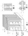
图1为一3D可编程电阻存储器阵列2×2部分的透视图,其中填充材料从图式中被移除,如此方能显示组成3D阵列的半导体带叠层以及垂直字线。在这张图式中,仅显示两个平面。然而,平面的数量可以扩展到非常大。如图1所示,存储器阵列被制造于一具有绝缘层10(insulating layer)的集成电路衬底上,其中绝缘层10以半导体或其它结构为基础(未绘示)。存储器阵列包括以绝缘材料21、22、23及24分离半导体带11、12、13及14的多个叠层。该多个叠层为延伸于Y轴的脊形,如图所示,如此半导体带11-14可被配置为存储器单元串行。半导体带11及13可用作第一存储器平面中的存储器单元串行。半导体带12及14可用作第二存储器平面中的存储器单元串行。存储器材料层15,例如为反熔丝材料,在本例中反熔丝材料涂覆于多个半导体带叠层上,而在其它例子中至少涂覆于半导体带的侧壁。多条字线16及17垂直跨越多个半导体带叠层而设置。字线16及17具有与多个半导体带叠层共形的表面,填补了多个叠层的边缘所形成的沟道(也就是图中的20),且使介于叠层上半导体带11-14侧面以及字线16及17侧面之间交叉点的接口区域的多层阵列成形。硅化物18及19(也就是硅化钨、硅化钴、硅化钛)的层可形成于字线16及17的顶面上。FIG. 1 is a perspective view of a 2×2 portion of a 3D programmable resistive memory array with fill material removed from the drawing so that the semiconductor strip stacks and vertical word lines that make up the 3D array are shown. In this drawing, only two planes are shown. However, the number of planes can be extended to be very large. As shown in FIG. 1, the memory array is fabricated on an integrated circuit substrate with an insulating layer 10 (insulating layer) based on a semiconductor or other structure (not shown). The memory array includes multiple stacks of semiconductor strips 11 , 12 , 13 and 14 separated by insulating
存储器材料层15可由反熔丝材料,例如二氧化硅、氮氧化硅或其它硅的氧化物所构成;举例来说存储器材料层15的厚度约为1至5纳米。存储器材料层15也可使用其它反熔丝材料,例如氮化硅。半导体带11-14可为第一导电类型(也就是P型)的半导体材料。字线16及17可为第二导电类型(也就是N型)的半导体材料。举例来说,半导体带11-14可使用P型多晶硅制造,反之字线16及17则可使用相对应的重掺杂N+型多晶硅(heavily doped n+-type polysilicon)制造。半导体带的宽度应提供耗尽层(depletion region)足够的空间以支持二极管运作。因此,包括以可编程反熔丝层P-N结(P-N junction)形成的整流器的存储器单元,是形成于多晶硅带及线之间的交叉点的3D阵列中。其中可编程反熔丝层位于阳极与阴极之间。在其它实施例中,可使用不同的可编程电阻存储器材料,包括像钨上的氧化钨或者掺杂金属氧化物半导体带之类的过渡金属氧化物(transition metal oxide)。这些材料可被编程及擦除,且可被实施于每单元储存多个位的作业。The
图2显示了从形成于字线16及半导体带14交叉区的存储器单元的X-Z平面所截取的截面图。有源区25及26是形成于介于字线16及带14之间的两个边上。于自然状态下,反熔丝材料层15具有高电阻。而在编程之后,反熔丝材料分解,致使反熔丝材料中的有源区25及26(activeregion)两者或其中之一呈现低电阻状态。于此描述的实施例中,每个存储器单元具有两个有源区25及26,各位于半导体带14的各个边缘。图3显示形成于字线16及半导体带14交叉区的存储器单元的X-Y平面截面图。图3也绘示了从标明为字线16的字线通过反熔丝材料层15而达半导体带14的电流路径。FIG. 2 shows a cross-sectional view taken from the X-Z plane of a memory cell formed at the intersection of
如图3中以实箭头绘示的电子流,从N+型字线16流入P型半导体带,然后沿半导体带(--箭头)流至感应放大器(sense amplifier),于其中该电子流可被测量,以指出选定存储器单元的状态。在将约1纳米厚二氧化硅层用作反熔丝材料的典型实施例中,编程脉冲是在一芯片上控制电路的控制下运用。其中该编程脉冲可包括具有约1毫秒脉冲宽度的5至7伏特脉冲,而该芯片上控制电路则描述于以下参照于图18的部分。读取脉冲是在一芯片上控制电路的控制下运用。其中该读取脉冲可包括1至2伏特脉冲,至于脉冲宽度则取决于其配置。该芯片上控制电路是描述于以下参照于图18的部分。读取脉冲可能远短于编程脉冲。The electron flow shown by the solid arrow in Fig. 3 flows from the N+
图4为显示存储器单元的2平面概要图,每个平面具有6个单元。存储器单元以带有虚线的二极管符号代表,该虚线代表了介于阳极与阴极之间的反熔丝材料层。位于字线60及61与半导体带51及52的第一叠层、半导体带53、54的第二叠层以及半导体带55及56的第三叠层的交叉点使两个平面的存储器单元成形,其中字线60及61作为第一字线(word line,WL)WLn及第二字线WLn+1,而第一至第三叠层则在第一层及第二层阵列中,作为存储单元串行n、n+1及n+2。存储器单元的第一平面包括了半导体带52上的存储器单元30及31、半导体带54上的存储器单元32及33以及半导体带56上的存储器单元34及35。存储器单元的第二平面包括了半导体带51上的存储器单元40及41、半导体带53上的存储器单元42及43以及半导体带55上的存储器单元44及45。如图所示,作为字线WLn的字线60,包括垂直延长部分60-1、60-2及60-3,其对应介于叠层之间而位于如图1所示的沟道20中的材料,该多个延伸部分乃是为了将字线60沿所绘示各平面中的3个材料带耦接于存储器单元。具有许多层的阵列可如于此所描述的来实施,使得非常高密度存储器的方法成为可能,或者达到每芯片万亿位(terabits per chip)。Figure 4 is a schematic diagram showing 2 planes of memory cells, each plane having 6 cells. A memory cell is represented by a diode symbol with a dashed line representing a layer of antifuse material between the anode and cathode. Two planar memory cells are formed at the intersections of
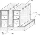
图5为一3D电荷设陷存储器阵列2×2部分的透视图,其中填充材料从图式中被移除,如此方能显示组成3D阵列的半导体带叠层以及垂直字线。在这张图式中,仅显示两个层。然而,层的数量可以扩展到非常大。如图5所示,存储器阵列被制造于一具有绝缘层110的集成电路衬底上,其中绝缘层110以半导体或其它结构为基础(未绘示)。存储器阵列包括以绝缘材料121、122、123及124分离半导体带111、112、113及114的多个叠层。该多个叠层为延伸于Y轴的脊形,如图所示,如此半导体带111-114可被配置为存储器单元串行。半导体带111及113可用作第一存储器平面中的存储器单元串行。半导体带112及114可用作第二存储器平面中的存储器单元串行。5 is a perspective view of a 2×2 portion of a 3D charge-trapping memory array with the fill material removed from the drawing so that the semiconductor strip stacks and vertical word lines making up the 3D array are shown. In this diagram, only two layers are shown. However, the number of layers can be scaled to be very large. As shown in FIG. 5, the memory array is fabricated on an integrated circuit substrate having an insulating
在第一叠层中介于半导体带111及112之间的绝缘层121以及在第二叠层中介于半导体带113及114之间的绝缘层123具有约40纳米或以上的有效氧化层厚度(effective oxide thickness,EOT),其中有效氧化层厚度是依据二氧化硅的介电常数比率(ratio of the dielectric constant)以及所选择的绝缘材料的介电常数而正规化(normalized)的绝缘材料厚度。用于此的词语「约40纳米」是为了估算进约10%左右的可能变动,如同传统上制造这型结构所产生的。绝缘材料的厚度在减少该结构的邻近层单元间的干扰可扮演关键角色。在某些实施例中,绝缘材料的有效氧化层厚度可小至30纳米并且同时让层与层之间有足够的隔离。The insulating
存储器材料层115,像是介电电荷设陷结构,在本实施例中涂覆在多个半导体带叠层上。多条字线116及117垂直跨越多个半导体带叠层而设置。字线116及117具有与多个半导体带叠层共形的表面,填补了多个叠层所形成的沟道(也就是图中的120),且使介于叠层上半导体带111-114的侧面以及字线116及117侧面之间交叉点的接口区域的多层阵列成形。硅化物118及119(也就是硅化钨、硅化钴、硅化钛)的层可形成于字线116及117的顶面上。A
纳米线金属氧化物半导体场效晶体管(metal-oxide-semiconductor fieldeffect transistor,MOSFET)单元也可用这种方式来设置,也就是透过在字线111-114上通道区中提供纳米线或者纳米管结构,如同Paul等人在2007年9月于电机与电子学工程会电子装置期刊第54册第9号所发表的「工艺变动对于纳米线与纳米管装置效能的影响」(”Impact of a ProcessVariation on Nanowire and Nanotube Device Performance”,IEEE Transactionson Electron Devices,Vol.54,No.9,September 2007)中所描述的,该文献在此被纳入参考,如同已被充分阐述(which article is incorporated by referenceas if fully set forth herein)。Nanowire metal-oxide-semiconductor field effect transistor (MOSFET) cells can also be arranged in this way, that is, by providing nanowire or nanotube structures in the channel region on the word lines 111-114. , as Paul et al. published "Impact of a Process Variation on the Performance of Nanowire and Nanotube Devices" ("Impact of a ProcessVariation on Nanowire and Nanotube Device Performance", IEEE Transactions on Electron Devices, Vol.54, No.9, September 2007), which article is incorporated by reference as if fully set forth herein).
如此可制造在NAND快闪阵列中配置的硅氧氮氧硅(silicon-oxide-nitride-oxide-silicon,SONOS)型存储器单元的3D阵列。源极(source)、漏极(drain)以及通道(channel)形成于硅半导体带111-114中,存储器材料层115包括可以二氧化硅形成的隧穿介电层97、可用氮化硅形成的电荷储存层98、可用二氧化硅形成的阻挡介电层99以及包括字线116及117的多晶硅的栅极。In this way, a 3D array of silicon-oxide-nitride-oxide-silicon (SONOS) type memory cells configured in a NAND flash array can be fabricated. The source (source), the drain (drain) and the channel (channel) are formed in the silicon semiconductor strips 111-114, and the
半导体带111-114可为P型半导体材料。字线116及117可为具相同或相异导电类型(也就是P+型)的半导体材料。举例来说,半导体带111-114可使用P型多晶硅或P型外延单晶硅制造,反之字线116及117则可使用相对应的重掺杂P+型多晶硅制造。The semiconductor strips 111-114 may be a P-type semiconductor material. The word lines 116 and 117 can be semiconductor materials with the same or different conductivity types (ie, P+ type). For example, the semiconductor strips 111-114 can be fabricated using P-type polysilicon or P-type epitaxial monocrystalline silicon, whereas the word lines 116 and 117 can be fabricated using corresponding heavily doped P+-type polysilicon.
另外,半导体带111-114可为N型半导体材料。字线116及117可为具相同或相异导电类型(也就是P+型)的半导体材料。这种N型带设置可达成隐通道(buried-channel)及消耗模式(depletion mode)电荷设陷存储器单元。举例来说,半导体带111-114可使用N型多晶硅或N型外延单晶硅(N-type epitaxial single crystal silicon)制造,反之字线116及117则可使用相对应的重掺杂P+型多晶硅制造。典型的N型半导体带掺杂浓度可在1018/cm3附近,以可用的实施例而言约在1017/cm3至1019/cm3的范围内。N型半导体带的使用在无结(junction-free)的实施例中特别有利于增进沿NAND串行的导电度且容许较高的读取电流。Additionally, the semiconductor strips 111-114 may be N-type semiconductor material. The word lines 116 and 117 can be semiconductor materials with the same or different conductivity types (ie, P+ type). This N-band arrangement enables buried-channel and depletion mode charge-trapping memory cells. For example, the semiconductor strips 111-114 can be made of N-type polysilicon or N-type epitaxial single crystal silicon (N-type epitaxial single crystal silicon), whereas the word lines 116 and 117 can be made of corresponding heavily doped P+-type polysilicon. manufacture. A typical N-type semiconductor strip doping concentration may be around 1018 /cm3 , in the range of about 1017 /cm3 to 1019 /cm3 for a useful embodiment. The use of N-type semiconductor strips is particularly beneficial in junction-free embodiments to improve conductivity along the NAND strings and allow for higher read currents.
如此,包括具有电荷储存结构的场效晶体管的存储器单元就被形成于交叉点的3D阵列中。使用约25纳米宽度的半导体带及字线,且于其中脊形间的间隙约为25纳米,一个具有几十个层(也就是32层)的装置就可在单芯片中达到万亿位的容量。In this way, memory cells including field effect transistors with charge storage structures are formed in a 3D array of cross points. Using semiconductor strips and word lines about 25nm wide, with a gap between ridges of about 25nm, a device with dozens of layers (
存储器材料层115可包括其它电荷储存结构。举例来说,可使用能隙设计SONOS(bandgap engineered SONOS,BE-SONOS)电荷储存结构,其包括介电隧穿层97,该介电隧穿层97包括在零偏压下形成倒「U」形价带的材料的合成物。在一实施例中,合成隧穿介电层包括称为空穴隧穿层(hole tunneling layer)的第一层、称为带偏移层(band offset layer)的第二层以及称为隔离层(isolation layer)的第三层。在此实施例中层115的空穴隧穿层包括在半导体带侧面上的二氧化硅,其形成举例来说是使用具选择性氮化物的原位蒸气生成法(in-situ steam generation,ISSG),其在沉积的过程中在周围环境既可使用后沉积一氧化氮退火(post depositionNO anneal)也可增加一氧化氮的使用。为二氧化硅的第一层的厚度小于

本实施例中的带偏移层包括平置于空穴隧穿层上的氮化硅,其形成举例来说是使用低压化学气相沉积法(low-pressure chemical vapor deposition,LPCVD),例如是在的680℃温度下使用二氯硅烷(dichlorosilane,DCS)及阿摩尼亚(NH3)前驱物。在替代的工艺中,带偏移层包括使用带有氧化二氮前驱物的相似工艺所制造的氮氧化硅。氮化硅带偏移层的厚度小于或更佳地小于等于
在此实施例中的隔离层包括二氧化硅,其平置于例如使用LPCVD高温氧化(high temperature oxide,HTO)沉积法而形成的氮化硅带偏移层上。二氧化硅隔离层的厚度小于
若价带能级所在的第一位置能使电场足以在介于带有半导体本体的接口与第一位置之间的薄区域诱导空穴隧穿,则价带能级就足将在第一位置之后的价带能级提升至能有效地消除第一位置之后的合成隧穿介电质中空穴隧穿势垒的位阶。这样的结构在三层隧穿介电层中建立了倒U形价带能级,且使得在高速下电场辅助(electric field assisted)的空穴隧穿成为可能,并同时有效地在没有电场或有因其它作业的目的而诱导的小电场时,(例如是在从单元读取数据或者编程相邻接的单元时)避免电荷的溢漏(leakage)通过合成隧穿介电质,。If the first position where the valence band energy level is located can make the electric field sufficient to induce tunneling of holes in the thin region between the interface with the semiconductor body and the first position, then the valence band energy level is sufficient to be at the first position The subsequent valence band energy level is raised to a level that effectively eliminates the hole tunneling barrier in the resultant tunneling dielectric after the first location. Such a structure establishes an inverted U-shaped valence band energy level in the three-layer tunneling dielectric layer, and enables electric field assisted (electric field assisted) hole tunneling at high speeds, while effectively operating in the absence of an electric field or Avoid charge leakage through the composite tunneling dielectric when there is a small electric field induced for other operational purposes, such as when reading data from a cell or programming an adjacent cell.
在一具代表性的装置中,存储器材料层115包括能隙设计合成隧穿介电层,其中包括了一厚度小于2纳米的二氧化硅层、一厚度小于3纳米的氮化硅层以及一厚度小于4纳米的二氧化硅层。在一实施例中,合成隧穿介电层包括了超薄二氧化硅层O1(也就是小于等于


在此实施例中的存储器材料层115中的电荷设陷层包括了厚度大于

在此实施例中的存储器材料层115中的阻挡介电层包括厚度大于

在一具代表性的实施例中,空穴隧穿层可为


图6显示了从形成于字线116及半导体带114接口的电荷设陷存储器单元的X-Z平面所截取的。有源电荷设陷区域125及126形成于介于字线116及带114之间的带114的两边上。在于此描述的实施例中,如图6所示,每个存储器单元皆为具有源电荷储存区域125及126的双栅极场效晶体管,且位于半导体带114的各边上。在图中以实箭头所绘示的电子流沿着P形半导体带而流动至感应放大器,于其中该电子流可被测量,以指出选定存储器单元的状态。FIG. 6 shows a section taken from the X-Z plane of a charge-trapping memory cell formed at the interface of
图7显示从形成于字线116及117与半导体带114的接口的电荷设陷存储器单元的X-Y平面所截取的截面图。顺半导体带114而下的电流路径也绘示于图中。即使缺乏具有与字线下通道区域相对的导电类型的源极与漏极掺杂,介于用作字线的字线116及117之间的源极/漏极区域128、129及130也可以是「无结」的。在无结的实施例中,电荷设陷场效晶体管可具有P型通道结构。并且,在某些实施例中可在字线成形之后在自校准注入(self-aligned implant)中实施源极与漏极掺杂。7 shows a cross-sectional view taken from the X-Y plane of a charge-trapping memory cell formed at the interface of
在替代的实施例中,半导体带111-114可在无结的设置中使用轻掺杂N型半导体主体来实施,如此便得到可在耗尽模式下运作的隐通道场效晶体管,且其具有电荷设陷单元的自然位移较低阀值分布(naturally shiftedlower threshold distribution)。In an alternative embodiment, the semiconductor strips 111-114 can be implemented in a junction-free setup using lightly doped N-type semiconductor bodies, thus resulting in hidden channel field effect transistors that can operate in depletion mode and have Naturally shifted lower threshold distribution of charge trapping cells.
图8是显示了具有在NAND配置中设置9个电荷设陷单元的存储器单元的2平面的概要图,其代表了可包括很多平面及很多字线的立方体。存储器单元的2平面定义于用作字线WLn-1及WLn的字线160及161与半导体带第一叠层、半导体带第二叠层以及半导体带第三叠层的交叉点。Figure 8 is a schematic diagram showing a 2-plane diagram of a memory cell with 9 charge trapping cells arranged in a NAND configuration, representing a cube that can include many planes and many word lines. 2 planes of the memory cell are defined at the intersections of
存储器单元的第一平面包括在半导体带上的NAND串行中的存储器单元70及71、在半导体带上的NAND串行中的存储器单元73、74以及在半导体带上的NAND串行中的存储器单元76、77。每个NAND串行的任一边连接至接地选择晶体管(也就是接地选择晶体管90及72连接至NAND串行70及71的任一边)。The first plane of memory cells includes
存储器单元第二平面在本例中对应至立方体中的底平面,且包括与第一平面类似的方法设置于NAND串行中的存储器单元(也就是80、82及84)。The second plane of memory cells corresponds in this example to the bottom plane in the cube, and includes memory cells (ie, 80, 82, and 84) arranged in NAND strings in a similar manner to the first plane.
如图所示,用作字线WLn的字线161包括对应于图5中介于叠层之间沟道120材料的垂直延长部分,这是为了将字线161耦接至所有平面中介于半导体带之间沟道中的接口区域的存储器单元(在第一平面中的单元71、74以及77)。As shown,
在相邻叠层中的存储器单元串行在位线端-至-来源线端导向(bit lineend-to-source line end orientation)与来源线端-至-位线端导向(source lineend-to-bit line end orientation)之间交替。Memory cells in adjacent stacks are serialized in bit line end-to-source line end orientation and source line end-to-bit line end orientation (source line end-to- bit line end orientation).
位线BLN及BLN-1(也就是96)为存储器串行的结尾,其与串行选择装置相邻。举例来说,在顶部存储器平面中,位线BLN为具有串行选择晶体管85及89的存储器单元串行的结尾。相比之下,位线并非连接至挽线88(trace),因为相邻叠层的串行在位线端-至-来源线端导向与来源线端-至-位线端之间交替。故反而对于此串行,相对应的位线是连接至串行的其它端。在底部的存储器平面中,位线BLN-1为具有相对应串行选择晶体管的存储器单元串行的结尾。Bit lines BLN and BLN-1 (ie, 96) are the end of the memory string, adjacent to the string select device. For example, in the top memory plane, bit line BLN is the end of the string of memory cells with string
串行选择晶体管85及89于此设置中在介于各自的NAND串行与串行选择线(string select line,SSL)SSLn-1及SSLn之间连接。同样地,在立方体中底部平面上类似的串行选择晶体管于此设置中在介于各自的NAND串行与串行选择线SSLn-1及SSLn之间连接。串行选择线106及108将不同的脊连接至在各个存储器单元串行中串行选择晶体管的栅极,以及在此实施例中提供串行选择讯号SSLn-1、SSLn及SSLn+1。String
相较之下,串行选择晶体管并不连接至挽线88,因为相邻叠层的串行在介于位线端-至-来源线端导向与来源线端-至-位线端导向之间交替。故反而对于此串行,相对应的串行选择晶体管是连结至串行的其它端。具存储器单元73及74的NAND串行也在串行的其它端上具有串行选择装置(并无绘示于图中)。挽线88以来源线107做结尾。In contrast, string select transistors are not connected to pull-up
接地选择晶体管90-95设置于NAND串行的第一端。接地选择晶体管72、75、78以及相对应的第二平面接地选择晶体管设置于NAND串行的第二端。因此,接地选择晶体管皆在存储器串行的两端上。依据存储器串行特定的端,接地选择晶体管将存储器串行耦接至来源线,或耦接至串行选择装置以及位线。Ground select transistors 90-95 are provided at the first end of the NAND string. The ground
于此实施例中的接地选择讯号GSL 159耦接于接地选择晶体管90-95的栅极,且可使用如字线160及161的相同方法来实施(其中159与162同样都是接地选择讯号GSL)。串行选择晶体管以及接地选择晶体管可如某些实施例中的存储器单元使用相同的介电叠层如栅极氧化层(gateoxide)。在其它实例中,就是使用典型的栅极氧化层。并且,通道长度与宽度可依设计者的需求作调校以提供晶体管的开关功能。Ground
图9为如图5的替代结构透视图。在此图中重复使用相似结构的参考数字,且于此不再重复描述。图9与图5的不同之处在于绝缘层110的表面110A以及半导体带113及114的侧面113A及114A是暴露于用作字线的字线116之间,此乃形成字线的刻蚀工艺的结果。因此,存储器材料层115可在不危害运作的情况下,在字线之间被完全地或部分地刻蚀。然而,类似于此描述地透过存储器层115刻蚀以形成介电电荷设陷结构在某些结构中并非必要。FIG. 9 is a perspective view of an alternative structure to that of FIG. 5 . Reference numerals for similar structures are reused in this figure and will not be described again here. The difference between FIG. 9 and FIG. 5 is that the
图10为类似于图6在X-Z平面中存储器单元的截面图。图10相同于图6,绘示了类似于图9的结构,其可得在此截面中如图5结构中实施的存储器单元。图11为类似于图7在X-Y平面中存储器单元的截面图。图11与图7不同的地方在于沿半导体带114的侧面(也就是114A)区域128a、129a以及130a的存储器材料可以被移除。10 is a cross-sectional view of a memory cell in the X-Z plane similar to FIG. 6 . FIG. 10 is identical to FIG. 6 and shows a structure similar to that of FIG. 9, which results in a memory cell implemented in the structure of FIG. 5 in this cross-section. Fig. 11 is a cross-sectional view of a memory cell in the X-Y plane similar to Fig. 7 . FIG. 11 differs from FIG. 7 in that the memory material in
图12-16绘示了如上述实施3D存储器阵列的基本流程阶段,其仅利用为阵列形成的关键校准步骤的2个图型掩模(pattern masking)步骤。在图12中,显示了在例如于芯片阵列区披覆沉积(blanket deposition)中使用掺杂半导体形成的绝缘层210、212、214以及半导体层211及213交替沉积所形成的结构。依据这样的实施方式,半导体层211及213可使用具有N型或P型掺杂的多晶硅或外延单晶硅来实施。跨级(inter-level)绝缘层210、212及214可使用例如二氧化硅、其它氧化硅或氮化硅来实施。这些层可用很多不同方法来形成,包括在所属技艺中可用的低压化学气相沉积工艺。Figures 12-16 illustrate the basic process stages for implementing a 3D memory array as described above, utilizing only 2 pattern masking steps which are key alignment steps for array formation. In FIG. 12 , a structure formed by alternating deposition of insulating
图13显示了用于使半导体带多个脊形叠层250成形的第一平板刻纹(lithographic patterning)步骤的结果,其中半导体带使用半导体层211及213的材料来实施,且被绝缘层212及214分离。深入地,高度高宽比(aspectratio)且支撑许多层的沟道可使用运用碳硬掩模(carbon hard mask)及反应离子刻蚀(reactive ion etching)的平板印刷基础的工艺来形成于叠层中。13 shows the result of a first lithographic patterning step for shaping a plurality of
虽然图中没有显示,然此步骤中存储器串行交替的导向是被定义为:位线端-至-来源线端导向以及来源线端-至-位线端导向。Although not shown in the figure, the alternating orientation of the memory series in this step is defined as: bit line end-to-source line end orientation and source line end-to-bit line end orientation.
图14A及14B相对地显示了包括可编程电阻存储器结构例如为反熔丝单元结构的实施例的下一阶段,以及包括可编程电荷设陷存储器结构如SONOS型存储器单元结构的实施例的下一阶段。14A and 14B relatively show the next stage of an embodiment including a programmable resistance memory structure, such as an antifuse cell structure, and the next stage of an embodiment including a programmable charge trapping memory structure, such as a SONOS-type memory cell structure. stage.
图14A显示了在一实施例中存储器材料层215的披覆沉积的结果,于该实施例中,存储器材料包括了类似于图一所示的反熔丝结构的单一层。在另一种实施例中,是运用氧化工艺而非披覆沉积,来在半导体带暴露的边上形成氧化物,其中氧化物是被用作存储器材料。FIG. 14A shows the result of blanket deposition of a
图14B显示了层315披覆沉积的结果,包括了包含隧穿层397、电荷设陷层398以及阻挡层399的多层电荷设陷结构,如同上述关于图4所描述的。如图14A及14B所示,存储器层215及315以共形的方式沉积于半导体带脊形叠层之上。Figure 14B shows the result of blanket deposition of
图15显示了高度宽高比填充步骤的结果,其中使用导电材料沉积形成层225以用作字线,该导电材料例如为N型或P型掺杂的多晶硅。并且,硅化物层226于利用多晶硅的实施例中可形成于层225之上。如此图所绘示,是利用于所绘示的实施例中的高度宽高比沉积技术例如多晶硅的低压化学气相沉积法来完全填充脊形叠层间的沟道220,即使该具高度高宽比并且非常狭窄的沟道窄至约10纳米。Figure 15 shows the result of a height aspect ratio fill step in which a
图16显示用于使3D存储器阵列中用作字线的多个字元线260成形的第二平板刻纹步骤的结果。第二平板刻纹步骤对于阵列关键的尺寸是利用单掩模来在字线之间刻蚀高度高宽比的沟道。可使用对多晶硅来说比二氧化硅与氮化硅还具高度选择性的刻蚀工艺来刻蚀多晶硅。因此,使用交替刻蚀工艺(alternating etch process)依靠相同的掩模来蚀穿导电与绝缘层,并止于作为基础的绝缘层210上。Figure 16 shows the results of the second slab scribing step for shaping a plurality of
于此步骤,也可使接地选择线成形。于此步骤,也可使被串行选择线所控制的栅极结构成形,即使栅极结构与个别半导体带叠层共形。At this step, the ground selection line may also be shaped. At this step, the gate structures controlled by the string select lines can also be shaped, ie the gate structures are conformal to the individual semiconductor strip stacks.
选择性的制造步骤包括了在多条字线上形成硬掩模,以及在栅极结构上形成硬掩模。硬掩模可使用相对薄的氮化硅层或其它可阻挡离子注入程序的材料而形成。在硬掩模形成之后,可实施注入以增加半导体带以及阶梯结构(stairstep structure)中的掺杂浓度,以减低沿半导体带电流路径的电阻。通过利用控制注入的能量,可致使注入物渗入至半导体带底部,且各自在叠层中覆盖半导体带。Optional fabrication steps include forming a hard mask over the plurality of word lines, and forming a hard mask over the gate structure. The hard mask can be formed using a relatively thin layer of silicon nitride or other material that blocks the ion implantation process. After the hard mask is formed, an implant can be performed to increase the doping concentration in the semiconductor strips and the staircase structure to reduce the resistance of the current path along the semiconductor strips. By utilizing controlled implant energy, the implants can be caused to penetrate to the bottom of the semiconductor strips and each cover the semiconductor strips in the stack.
随后,移除硬掩模,暴露沿字线顶面以与栅极结构上的硅化物层。在阵列顶部上形成一夹层介电质(interlayer dielectric)之后,通孔(via)会被开启,在通孔中,例如使用钨填充的接触栓(contact plug)被形成到达至栅极结构的顶面。覆盖金属线被刻纹以如SSL线般连接至列译码器电路。一个三平面的译码网络是被建立,其使用一条字线、一条位线以及一条SSL线来存取选定单元。请见标题为「平面译码方法及3D存储器装置」(Plane Decoding Method and Device for Three Dimensional Memories)的第6906940号美国专利。Subsequently, the hard mask is removed, exposing the silicide layer along the top surface of the word line and on the gate structure. After forming an interlayer dielectric on top of the array, vias are opened in which contact plugs, for example filled with tungsten, are formed to reach the top of the gate structure. noodle. The cover metal lines are patterned to connect to the column decoder circuits as SSL lines. A three-plane decode network is built that uses a word line, a bit line and an SSL line to access selected cells. See US Patent No. 6,906,940 entitled "Plane Decoding Method and Device for Three Dimensional Memories."
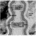
图17为一张已被模拟及测试过的8层垂直栅、薄膜晶体管以及BE-SONOS电荷设陷NAND装置的部分TEM剖面图。该装置是以75纳米是半节距(half pitch)制造。通道为约18纳米厚的N型多晶硅。不使用额外的结注入,成为无结的结构。隔离Z方向通道而介于带之间的绝缘材料为约40纳米厚的二氧化硅。以P+多晶硅线来提供栅极。SSL与GSL装置具有较存储器单元长的通道长度。该测试装置实施了32条字线及无结的NAND串行。因为用于形成该结构的沟道刻蚀造成具有随沟道渐深而渐宽的带的锥形侧墙,且因为锥形侧墙具有介于相对于多晶硅被刻蚀较多的带之间的绝缘材料,所以图17中的较低带的宽度大于较高带的宽度。Fig. 17 is a partial TEM cross-sectional view of a simulated and tested 8-layer vertical gate, TFT and BE-SONOS charge-trapping NAND device. The device is fabricated at a half pitch of 75nm. The channel is N-type polysilicon about 18 nanometers thick. No additional junction injection is used, resulting in a junction-free structure. The insulating material between the ribbons isolating the Z-direction channels is about 40 nanometers thick silicon dioxide. The gate is provided by a P+ polysilicon line. SSL and GSL devices have longer channel lengths than memory cells. The test set implements 32 word lines and junctionless NAND strings. Because the trench etch used to form the structure results in tapered sidewalls with bands that get wider as the trench gets deeper, and because the tapered sidewalls have intervening bands that are more etched relative to polysilicon The insulating material, so the width of the lower band in Figure 17 is greater than the width of the upper band.
图17显示了具有不同侧边尺寸的3D结构的不同层。这种在层之间的不同侧边尺寸是3D结构不同层之间不同电容的来源。Figure 17 shows different layers of the 3D structure with different side dimensions. This different side dimension between the layers is the source of the different capacitance between the different layers of the 3D structure.
图18为根据本发明实施例的集成电路简化方框图。集成电路线路875包括了如在此描述般实施的3D可编程电阻存储器阵列860(resistedrandom-access memory,RRAM),其位于半导体衬底之上,具有位线端-至-来源线端导向与来源线端-至-位线端导向的交替存储器串行导向,且位于在所有其它叠层之上的串行选择线栅极结构叠层的任一端。列译码器861耦接至多条字线862,且沿存储器阵列860的行而设置。行译码器863耦接至沿对应于存储器阵列860中叠层的行而设置的多条SSL线864,以从阵列860中的存储器单元读取及编程数据。平面译码器858耦接至位线859上存储器阵列860中的多个平面。在总线865上提供地址给行译码器863、列译码器861以及平面译码器858。方块866中的感应放大器及数据输入(data-in)结构在此实施例中透过数据总线867耦接至行译码器863。数据是从集成电路875上的输入/输出端口透过数据输入线871而提供,或者从其它集成电路875内部或外部的数据来源提供至方块866中的数据输入结构。在所绘示的实施例中,集成电路包括了其它的电路系统874,例如一般用途处理器或特定用途应用电路系统,或者是提供可编程电阻单元阵列支持的芯片上系统(system-on-a-chip)功能模块的组合。数据是从方块866中的感应放大器透过数据输出(data-out)线872提供至集成电路875上的输入/输出端,或提供至其它集成电路875内部或外部的数据目的地。Figure 18 is a simplified block diagram of an integrated circuit according to an embodiment of the present invention. Integrated
使用偏压设置状态机869(bias arrangement state machine)的本实施例中所实施的控制器,是用来控制透过方块868中一个或多个电压供应器所产生或提供的偏压设置供应电压的应用,例如读取及编程电压。控制器可使用熟知技艺中的特定用途逻辑电路系统来实施。在一替代实施例中,控制器包括了一般用途处理器,控制器可在相同的集成电路上实施,而所包括的一般用途处理器则执行计算机程序来控制装置的运作。又在另一个实施例中,可利用特定用途逻辑电路系统及一般用途处理器的组合以实施其它控制器。The controller implemented in this embodiment using a bias arrangement state machine 869 (bias arrangement state machine) is used to control the bias arrangement supply voltage generated or provided by one or more voltage supplies in
图19为依据本发明一实施例的集成电路的简化方块图。集成电路线路975包括了如这里所描述而实施的半导体衬底上具有交替存储器串行导向的3D NAND闪存阵列960,且位于具有所有其它叠层上都有的串行选择线栅极结构的叠层的任一端,所谓交替存储器串行导向为位线端-至来源线端导向以及来源线端-至-位线端导向。列译码器961耦接至多条字线962,且沿存储器阵列960中的列而设置。行译码器963耦接至沿对应于存储器阵列960中叠层的行而设置的多条SSL线964以从阵列960中的存储器单元读取及编程数据。平面译码器958透过位线959耦接至存储器阵列960中的多个平面。在总线965(bus)上提供地址给行译码器963(columndecoder)、列译码器961(row decoder)以及平面译码器958(plane decoder)。方块966中的感应放大器及数据输入结构在此实施例中透过数据总线967耦接至行译码器963。数据是从集成电路975上的输入/输出端口透过数据输入线971而提供,或者从其它集成电路975内部或外部的数据来源提供至方块966中的数据输入结构。在所绘示的实施例中,集成电路包括了其它的电路系统974,例如一般用途处理器或特定用途应用电路系统,或者是提供可编程电阻单元阵列支持的芯片上系统功能模块的组合。数据是从方块966中的感应放大器透过数据输出线972提供至集成电路975上的输入/输出端口,或提供至其它集成电路975内部或外部的数据目的地。Figure 19 is a simplified block diagram of an integrated circuit according to one embodiment of the invention. Integrated
使用偏压设置状态机969的本实施例中所实施的控制器,是用来控制透过方块968中一个或多个电压供应器所产生或提供的偏压设置供应电压的应用,例如读取、擦除、编程、擦除验证(erase verify)以及编程验证(program verify)电压。控制器可使用熟知技艺中的特定用途逻辑电路系统来实施。在一替代实施例中,控制器包括了一般用途处理器,控制器可在相同的集成电路上实施,而所包括的一般用途处理器则执行计算机程序来控制装置的运作。又在另一个实施例中,可利用特定用途逻辑电路系统及一般用途处理器的组合以实施其它控制器。The controller implemented in this embodiment using the bias setting
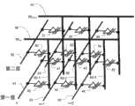
图20-22绘示了具有平行于半导体材料带的纵向导向串行选择线、平行于字线的横向导向串行选择线以及平行于半导体材料带的纵向导向位线的渐高金属层的第一3D NAND闪存阵列结构。Figures 20-22 illustrate a first metal layer of progressively higher metal layers with vertically oriented serial select lines parallel to the strips of semiconductor material, laterally oriented serial select lines parallel to the word lines, and vertically oriented bit lines parallel to the semiconductor material strips A 3D NAND flash memory array structure.
图20为第一3D NAND闪存阵列结构的透视图。绝缘材料从图式中被移除以暴露附加的结构。举例来说,绝缘层在脊形叠层中的半导体带间被移除,且在半导体带的脊形叠层之间被移除。20 is a perspective view of the first 3D NAND flash memory array structure. Insulating material has been removed from the drawings to expose additional structures. For example, the insulating layer is removed between the semiconductor strips in the ridge stack, and between the ridge stacks of semiconductor strips.
多层阵列形成于绝缘层之上,且包括了共形于多个脊形叠层的多条字线425-1、…、425-n-1及425-n,该多条字线被用作字线WLn、WLn-1、…WL1。多个脊形叠层包括了半导体带412、413、414及415。在相同平面中的半导体带与阶梯结构电性耦接在一起。A multilayer array is formed over the insulating layer and includes a plurality of wordlines 425-1, . . . , 425-n-1, and 425-n conformal to a plurality of Word lines WLn, WLn-1, . . . WL1 are used. The plurality of ridge stacks includes semiconductor strips 412 , 413 , 414 and 415 . The semiconductor strips in the same plane are electrically coupled with the ladder structure.
所示的字线编号,其从结构的后端到前端依序从1至N渐大,是应用于偶数内存页。对于奇数内存页,字线编号从结构的后端到前端依序则从N至1渐小。The word line numbers shown, which are sequentially increased from 1 to N from the back end of the structure to the front end, are applied to even memory pages. For odd memory pages, the number of word lines gradually decreases from N to 1 from the back end of the structure to the front end.
阶梯结构412A、413A、414A及415A为半导体带的结尾,例如为半导体带412、413、414及415的结尾。如图所示,这些阶梯结构412A、413A、414A及415A电性连接至不同位线来将译码电路系统连接至阵列中的选择平面。这些阶梯结构412A、413A、414A及415A可于使多个脊形叠层成形的同时被刻纹。The stepped
阶梯结构402B、403B、404B及405B为半导体带的结尾,例如为半导体带402、403、404及405的结尾。如图所示,这些阶梯结构402B、403B、404B及405B电性连接至不同位线来将译码电路系统连接至阵列中的选择平面。这些阶梯结构402B、403B、404B及405B可于使多个脊形叠层成形的同时被刻纹。The stepped
任何给定的半导体带叠层不是被耦接至阶梯结构412A、413A、414A及415A,就是被耦接至阶梯结构402B、403B、404B及405B,但并不耦接至两者。半导体带叠层具有位线端-至-来源线端导向或来源线端-至-位线端导向的两相对导向其中之一。举例来说,半导体带412、413、414及415的叠层具有位线端-至-来源线端导向,而半导体带402、403、404及405的叠层则具有来源线-至-位线端导向。Any given semiconductor ribbon stack is coupled to either
导体带412、413、414及415的叠层通过阶梯结构412A、413A、414A及415A在其中一端结尾,通过SSL栅极结构419、栅极选择线GSL426、从字线425-1WL至425-N WL、栅极选择线GSL427,然后透过来源线428结尾于另一端。半导体带412、413、414及415的叠层并不到达阶梯结构402B、403B、404B及405B。The stack of conductor strips 412, 413, 414, and 415 terminates at one end through
半导体带402、403、404及405的叠层通过阶梯结构402B、403B、404B及405B在其中一端结尾,通过SSL栅极结构409、栅极选择线GSL427、从字线425-NWL至425-1WL、栅极选择线GSL426,然后透过来源线(被图示的其它部分所遮盖)结尾于另一端。半导体带402、403、404及405的叠层并不到达阶梯结构412A、413A、414A及415A。The stack of semiconductor strips 402, 403, 404, and 405 terminates at one end through
如前图所详细描述的,存储器材料层从半导体带412-415以及402-405分离了字线425-1至425-n。接地选择线GSL 426及GSL 427共形于多个脊形叠层,类似于字线。As detailed in previous figures, the layer of memory material separates the word lines 425-1 to 425-n from the semiconductor strips 412-415 and 402-405. Ground
半导体带的每个叠层的其中一端皆以阶梯结构做结尾,并且以来源线做为另一端的结尾。举例来说,半导体带412、413、414及415的叠层透过阶梯结构412A、413A、414A及415A结尾于其中一端,并透过来源线428结尾于另一端。在本图的近端,一部分的半导体带叠层透过阶梯结构402B、403B、404B及405B结尾,而所有另一部分的半导体带叠层则透过来源线结尾。在本图的远程,该所有另一部分的半导体带叠层透过阶梯结构412A、413A、414A及415A,而该一部分的半导体带叠层则透过来源线结尾。Each stack of semiconductor strips terminates at one end in a ladder structure and at the other end in a source line. For example, the stack of semiconductor strips 412 , 413 , 414 and 415 terminates at one end through
位线及串行选择线形成于金属层ML1、ML2以及ML3,且讨论于较明显的下图。Bit lines and string select lines are formed on metal layers ML1, ML2, and ML3, and are discussed more clearly below.
晶体管于阶梯结构412A、413A、414A及字线425-1之间形成。在晶体管中,半导体带(也就是413)用作装置的通道区域。SSL栅极结构(也就是419及409)在使字线425-1至425-n成形的相同步骤期间被刻纹。硅化物层可沿字线425-1至425-n与接地选择线426及427的顶面形成,以及形成于栅极结构409及419之上。存储器材料415的层可用做晶体管的栅极介电质。这些晶体管用作耦接于译码电路系统的串行选择栅极,以选择阵列中的特定脊形叠层。Transistors are formed between the
图21及22绘示图20所示的第一3D NAND闪存阵列结构的侧图。图21显示了所有三个金属层ML1、ML2及ML3。图22显示了较低的两个金属层ML1及ML2,其中移除了第三金属层ML3以使其它金属层较容易检视。21 and 22 are side views of the structure of the first 3D NAND flash memory array shown in FIG. 20. Figure 21 shows all three metal layers ML1, ML2 and ML3. Figure 22 shows the lower two metal layers ML1 and ML2 with the third metal layer ML3 removed to allow easier inspection of the other metal layers.
第一金属层ML1包括了具平行于半导体材料带的纵向导向的串行选择线。这些ML1串行选择线透过短通孔而连接至不同的SSL栅极结构(也就是409及419)。The first metal layer ML1 includes serial select lines with a longitudinal orientation parallel to the strips of semiconductor material. These ML1 serial select lines are connected to different SSL gate structures (
第二金属层ML2包括了具平行于字线的横向导向的串行选择线。这些ML2串行选择线透过短通孔而连接至不同的ML1串行选择线。The second metal layer ML2 includes serial select lines with a lateral orientation parallel to the word lines. These ML2 string select lines are connected to different ML1 string select lines through short vias.
相结合后,这些ML1串行选择线以及ML2串行选择线容许了使用串行选择讯号来选择半导体带的特定叠层。In combination, these ML1 string select lines and ML2 string select lines allow string select signals to be used to select a particular stack of semiconductor strips.
第一金属层ML1也包括了两条具有平行于字线的横向导向的来源线。The first metal layer ML1 also includes two source lines with a lateral orientation parallel to the word lines.
最后,第三金属层ML3包括了具有平行于半导体材料带的纵向导向的位线。不同位线电性连接至阶梯结构412A、413A、414A及415A及402B、403B、404B及405B的不同阶。这些ML3位线容许了使用位线讯号来选择半导体带的特定水平平面。Finally, the third metal layer ML3 comprises bit lines with a longitudinal orientation parallel to the strips of semiconductor material. Different bit lines are electrically connected to different levels of the
因为特定字线容许了字线选择存储器单元的特定列平面,字线讯号、位线讯号以及串行选择线讯号的三重组合足以从存储器单元的3D阵列中选择特定存储器单元。Since a specific word line allows the word line to select a specific column plane of memory cells, a triple combination of the word line signal, the bit line signal, and the string select line signal is sufficient to select a specific memory cell from a 3D array of memory cells.
图23-26绘示具有平行于字线的横向导向串行选择线、平行于半导体带的纵向导向串行选择线以及平行于半导体材料带的纵向导向位线的渐高金属层的第一3D NAND闪存阵列结构。23-26 illustrate a first 3D metal layer with progressively higher metal layers with laterally oriented serial select lines parallel to the word lines, vertically oriented serial select lines parallel to the semiconductor strips, and vertically oriented bit lines parallel to the semiconductor material strips. NAND flash array structure.
图23-图26所示的第二3D NAND闪存阵列大致与图20-图22所示的第一3D NAND闪存阵列相似。为了更利于检视,图26进一步地移除所有的三个金属层ML1、ML2及ML3。The second 3D NAND flash memory array shown in FIGS. 23-26 is substantially similar to the first 3D NAND flash memory array shown in FIGS. 20-22. For better viewing, all three metal layers ML1 , ML2 and ML3 are further removed in FIG. 26 .
然而,图23-图26所示的第二3D NAND闪存阵列显示了32条字线,而图20-图22所示的第一3D NAND闪存阵列则显示了8条字线。而其它的实施例则具有不同数量的字线、位线以及串行选择线,以及相对应不同数量的半导体带叠层等等。However, the second 3D NAND flash array shown in Figures 23-26
并且,图23-图26所示的第二3D NAND闪存阵列显示了以多晶硅栓将接触栓连接至阶梯结构的不同阶,而图20-图22所示的第一3D NAND闪存阵列则显示将ML3位线连接至阶梯结构不同阶的金属接触栓。Also, the second 3D NAND flash array shown in Figures 23-26 shows polysilicon plugs connecting the contact plugs to different levels of the ladder structure, while the first 3D NAND flash array shown in Figures 20-22 shows the The ML3 bit line is connected to the metal contact plugs of different steps of the ladder structure.
进一步地,图23-图26所示的第二3D NAND闪存阵列具有通往ML1译码器的串行选择线以及通往ML2上SSL栅极结构的串行选择线,而图20-图22所示的第一3D NAND闪存阵列则具有通往在ML2译码器的串行选择线以及通往ML1上SSL栅极结构的串行选择线。Further, the second 3D NAND flash memory array shown in Figures 23-26 has a serial selection line leading to the ML1 decoder and a serial selection line leading to the SSL gate structure on ML2, while Figures 20-22 The first 3D NAND flash array shown has a string select line to the decoder at ML2 and a string select line to the SSL gate structure on ML1.
图27为图20-图22的第一3D NAND闪存阵列结构设计图。FIG. 27 is a structural design diagram of the first 3D NAND flash memory array shown in FIG. 20-FIG. 22.
在图27的设计图中,半导体带叠层显示为具点-破折号边缘的垂直带。相邻的半导体带叠层在相对的导向之间交替,也就是在位线端-至-来源线端导向以及来源线端-至-位线端导向之间交替。一部分的半导体带叠层从顶部的位线结构运行至底部的来源线结构。所有另一部分的半导体带叠层则从顶部的来源线结构运行至底部的位线结构。In the design diagram of Figure 27, the semiconductor ribbon stack is shown as a vertical ribbon with dot-dash edges. Adjacent stacks of semiconductor strips alternate between opposite orientations, ie, bitline-to-source-line orientations and source-to-bitline-end orientations. A portion of the semiconductor strip stack runs from the bit line structure at the top to the source line structure at the bottom. All other parts of the semiconductor strip stack run from the source line structure at the top to the bit line structure at the bottom.
覆盖半导体带叠层的是水平字线以及水平接地选择线GSL(偶)与GSL(奇)。覆盖半导体带叠层的并且为SSL栅极结构。SSL栅极结构在半导体带顶端覆盖了一部分半导体带叠层,且在半导体带底端覆盖了所有其它半导体带叠层。在这两种情况下,SSL栅极结构皆控制任何半导体带叠层与对应于叠层的位线接触结构之间的电性连接。Overlying the semiconductor strip stack are horizontal word lines and horizontal ground select lines GSL(even) and GSL(odd). Overlying the semiconductor tape stack is an SSL gate structure. The SSL gate structure covers a portion of the semiconductor ribbon stack at the top of the semiconductor ribbon and covers all other semiconductor ribbon stacks at the bottom of the semiconductor ribbon. In both cases, the SSL gate structure controls the electrical connection between any semiconductor strip stacks and the bit line contact structures corresponding to the stacks.
所示的字线编号,其从图顶至图底依序从1至N渐大,是应用于偶数内存页。对于奇数内存页,字线编号从图顶至图底依序则从N至1渐小。The word line numbers shown, which increase sequentially from 1 to N from the top of the figure to the bottom of the figure, are for even memory pages. For odd-numbered memory pages, the number of word lines decreases from N to 1 from the top of the figure to the bottom of the figure.
覆盖字线、接地选择线以及SSL栅极结构的是垂直运行的ML1 SSL串行选择线。覆盖ML1 SSL串行选线的是水平运行的ML2 SSL串行选择线。虽然ML2 SSL串行选择线为了能容易检视结构而显示为相对应ML1SSL串行选择线的结尾,但ML2 SSL串行选择线的水平运行可以更加延长。ML2 SSL串行选择线传送从译码器来的讯号,而ML1 SSL串行选择线耦接这些译码器讯号至特定SSL栅极结构以选择特定半导体带叠层。Overlaying the word lines, ground select lines, and SSL gate structures are ML1 SSL serial select lines running vertically. Overlaying the ML1 SSL serial select line is the ML2 SSL serial select line running horizontally. Although the ML2 SSL serial select lines are shown corresponding to the end of the ML1 SSL serial select lines for ease of structural inspection, the horizontal run of the ML2 SSL serial select lines can be extended further. The ML2 SSL serial select lines carry signals from the decoders, while the ML1 SSL serial select lines couple these decoder signals to specific SSL gate structures to select specific semiconductor strip stacks.
覆盖ML1 SSL串行选择线的并且是奇数号与偶数号的来源线。Odd and even numbered source lines that cover the ML1 SSL serial select lines.
进一步地,覆盖ML2 SSL串行选择线的是于顶端及底端连接至阶梯接触结构(stepped contact structure)的ML3位线(并无显示于图中)。透过阶梯接触结构,位线能选择半导体带的特定平面。Further, overlying the ML2 SSL serial select line is the ML3 bit line (not shown) connected to a stepped contact structure at the top and bottom. Through the stepped contact structure, the bit line can select a specific plane of the semiconductor strip.
图28为图23-图26第二3D NAND闪存阵列结构的设计图。图28所示的这个第二3D NAND闪存阵列结构大致与图27所示的第一3D NAND闪存结构设计图相似。然而,图28所示的第二3D NAND闪存阵列具有通往ML1译码器的串行选择线以及通往ML2上SSL栅极结构的串行选择线,而图27显示的第一3D NAND闪存结构则具有通往ML2译码器的串行选择线以及通往ML1上SSL栅极结构的串行选择线。Fig. 28 is a design diagram of the second 3D NAND flash memory array structure in Fig. 23-Fig. 26. This second 3D NAND flash memory array structure shown in Figure 28 is roughly similar to the first 3D NAND flash memory structure design shown in Figure 27. However, the second 3D NAND flash array shown in Figure 28 has a serial select line to the decoder of ML1 and a serial select line to the SSL gate structure on ML2, whereas the first 3D NAND flash array shown in Figure 27 The structure then has a string select line to the ML2 decoder and a string select line to the SSL gate structure on ML1.
图29为3D存储器阵列的平面图。在所示的阵列中,Y半节距=32纳米而X半节距=43纳米。在3D VG NAND中有4个存储器层。阵列中的核心使用率(core efficiency)约为67%(66条WL,与其上的SSL栅极、GSL、SL以及BL接点)。以单阶单元(single level cell)运作时(1b/c)其密度为32Gb。芯片面积大小约为76mm2。Fig. 29 is a plan view of a 3D memory array. In the array shown, Y half-pitch = 32nm and X half-pitch = 43nm. There are 4 memory layers in 3D VG NAND. The core efficiency in the array is about 67% (66 WLs with SSL gates, GSL, SL and BL contacts on them). When operating as a single level cell (1b/c), its density is 32Gb. The chip area size is about 76mm2 .
图30绘示具有平行于字线的横向导向串行选择线、平行于半导体带的纵向导向串行选择线以及平行于半导体材料带的纵向导向位线的渐高金属层的3D NAND闪存阵列结构。图30相似于图23。图30相较于图23的更动为将第一组阵列层编号(1)-(4)增加至位线,以及将第二组阵列层编号(1)-(4)增加至包括阶梯结构402B、403B、404B及405B的位线结构。这些阵列层编号组乃用以显示特定位线电性连接至特定阵列层位置。30 shows a 3D NAND flash memory array structure with progressively higher metal layers with laterally oriented serial select lines parallel to word lines, vertically oriented serial select lines parallel to semiconductor strips, and vertically oriented bit lines parallel to semiconductor material strips . FIG. 30 is similar to FIG. 23 . The modification of FIG. 30 compared to FIG. 23 is that the first set of array layer numbers (1)-(4) is added to the bit lines, and the second set of array layer numbers (1)-(4) is added to include a ladder structure Bit line structures of 402B, 403B, 404B and 405B. These array layer number sets are used to indicate that a specific bit line is electrically connected to a specific array layer position.
图30显示了具有1、2、3及4平面位置序列的存储器区块。相对应地,如同位线结构从第一端横越至第二端,连续编号的位线1-4(也就是从左至右、从右至左或其它连续的顺序来编号)通过阶梯接触结构(也可称之为位线结构)耦接至平面位置1-4(也就是从顶到底、从底到顶或其它顺序来编号)。Figure 30 shows a memory block with a sequence of 1, 2, 3 and 4 plane locations. Correspondingly, as the bit line structure traverses from the first end to the second end, consecutively numbered bit lines 1-4 (that is, numbered from left to right, from right to left or other continuous order) pass through the stepped contact structure (Alternatively referred to as bit line structures) are coupled to planar positions 1-4 (ie numbered from top to bottom, bottom to top or other order).
图31为具有以特定位线存取阵列层的编号标示的位线的3D NAND闪存阵列结构设计图。在所示的范例中,如同依序横越的4条位线(也就是从左至右、从右至左或其它顺序来编号),也将位线以平面位置1、2、3及4来标示。所以如同依序横越的4条位线,也将位线通过以破折号方框显示的阶梯接触结构(也可称之为位线结构)耦接至平面位置1-4(也就是从顶至底、从底至顶或其它顺序来编号)。FIG. 31 is a structural design diagram of a 3D NAND flash memory array with bit lines marked with numbers of specific bit line access array layers. In the example shown, the bitlines are also numbered in
图32为具有以位线存取的阵列层的编号标示的位线3D NAND闪存阵列结构设计图,显示了相邻具有以不同序列耦接至阵列层的位线的区块。FIG. 32 is a structural design diagram of a 3D NAND flash memory array with bit lines indicated by the numbers of the array layers accessed by the bit lines, showing adjacent blocks with bit lines coupled to the array layers in different sequences.
图32显示了不同位线结构具有平面位置的平移序列。举例来说,所显示的不同位线结构平面位置的不同序列为1、2、3及4;2、3、4及1;以及3、4、1及2。相对应地最左边从顶运行至底且连接于不同位线结构的位线,被连接至平面位置1、2及3(以从顶位线结构至底位线结构的顺序)。第二左边从顶运行至底且连接至不同位线结构的位线,被连接至平面位置2、3及4(以从顶位线结构至底位线结构的顺序)。第三左边从顶运行至底且连接至不同位线结构的位线,被连接至平面位置3、4及1(以从顶位线结构至底位线结构的顺序)。第四左边从顶运行至底且连接至不同位线结构的位线,被连接至平面位置4、1及2(以从顶位线结构至底位线结构的顺序)。Figure 32 shows a translation sequence with planar positions for different bit line configurations. For example, different sequences of different bit line structure plane positions are shown as 1, 2, 3 and 4; 2, 3, 4 and 1; and 3, 4, 1 and 2. Correspondingly the leftmost bitlines running from top to bottom and connected to different bitline structures are connected to
在某些实施例中,选择位线结构的编号以及存储器区块的编号是为了使每条字线皆如其它字线具有相同的所谓之电容,其原因为耦接的为相同于其它位线的平面位置组合。In some embodiments, the numbering of the bitline structures and the numbering of the memory blocks are chosen so that each wordline has the same so-called capacitance as the other wordlines, because the coupling is the same as the other bitlines combination of plane positions.
多种实施例包括了不同数量的位线以及不同数量的耦接至位线的平面位置,例如两倍或二次方。Various embodiments include different numbers of bit lines and different numbers of plane locations coupled to the bit lines, such as double or quadratic.
虽本发明已以较佳实施例及范例详述如上,然需知其乃用以举例说明而非限定本发明。本发明所属技术领域中具有通常知识者,在不脱离本发明的精神和范围内,当可作各种的更动与润饰。因此,本发明的保护范围当视随附的权利要求范围所界定的为准。Although the present invention has been described above in detail with preferred embodiments and examples, it should be understood that they are for illustration rather than limitation of the present invention. Those skilled in the art of the present invention can make various changes and modifications without departing from the spirit and scope of the present invention. Therefore, the protection scope of the present invention should be defined by the appended claims.
Claims (20)
Translated fromChineseApplications Claiming Priority (4)
| Application Number | Priority Date | Filing Date | Title |
|---|---|---|---|
| US201161434350P | 2011-01-19 | 2011-01-19 | |
| US61/434,350 | 2011-01-19 | ||
| US13/239,760US8811077B2 (en) | 2011-01-19 | 2011-09-22 | Memory architecture of 3D array with improved uniformity of bit line capacitances |
| US13/239,760 | 2011-09-22 |
Publications (2)
| Publication Number | Publication Date |
|---|---|
| CN102709269Atrue CN102709269A (en) | 2012-10-03 |
| CN102709269B CN102709269B (en) | 2014-11-19 |
Family
ID=46901927
Family Applications (1)
| Application Number | Title | Priority Date | Filing Date |
|---|---|---|---|
| CN201110344095.5AActiveCN102709269B (en) | 2011-01-19 | 2011-11-04 | 3D Array Memory Device with Improved Uniformity of Bit Line Capacitance |
Country Status (2)
| Country | Link |
|---|---|
| CN (1) | CN102709269B (en) |
| TW (1) | TWI490862B (en) |
Cited By (10)
| Publication number | Priority date | Publication date | Assignee | Title |
|---|---|---|---|---|
| CN103928042A (en)* | 2013-01-16 | 2014-07-16 | 旺宏电子股份有限公司 | Method for operating multi-bit memory cell |
| CN103928054A (en)* | 2013-01-15 | 2014-07-16 | 旺宏电子股份有限公司 | Memory including stacked memory structure and operation method thereof |
| CN104319276A (en)* | 2014-09-16 | 2015-01-28 | 华中科技大学 | Gate electrode for nonvolatile three-dimensional semiconductor memory, and preparation method for gate electrode |
| CN104599712A (en)* | 2013-10-31 | 2015-05-06 | 旺宏电子股份有限公司 | Stacked 3D memory and manufacturing method thereof |
| TWI495173B (en)* | 2013-03-13 | 2015-08-01 | Macronix Int Co Ltd | Integrated circuit device and method for manufacturing semiconductor and memory device |
| CN105097816A (en)* | 2014-05-08 | 2015-11-25 | 旺宏电子股份有限公司 | Integrated circuit, structure of multi-layer device and manufacturing method thereof |
| CN105453266A (en)* | 2013-07-01 | 2016-03-30 | 美光科技公司 | Semiconductor devices including stair step structures, and related methods |
| CN105990354A (en)* | 2015-01-28 | 2016-10-05 | 旺宏电子股份有限公司 | Memory element and manufacturing method thereof |
| CN110896078A (en)* | 2018-08-23 | 2020-03-20 | 旺宏电子股份有限公司 | Memory element and manufacturing method thereof |
| WO2020063359A1 (en)* | 2018-09-25 | 2020-04-02 | 成都皮兆永存科技有限公司 | Producing method for programmable memory |
Families Citing this family (9)
| Publication number | Priority date | Publication date | Assignee | Title |
|---|---|---|---|---|
| TWI512729B (en)* | 2012-08-23 | 2015-12-11 | Macronix Int Co Ltd | Semiconductor structure with improved capacitance of bit line |
| TWI552336B (en)* | 2014-12-16 | 2016-10-01 | 旺宏電子股份有限公司 | Higher aspect ratio structure of semiconductor device |
| US9679807B1 (en) | 2015-11-20 | 2017-06-13 | Globalfoundries Inc. | Method, apparatus, and system for MOL interconnects without titanium liner |
| US10566253B2 (en) | 2017-11-30 | 2020-02-18 | Nanya Technology Corporation | Electronic device and electrical testing method thereof |
| US10929588B2 (en)* | 2018-02-13 | 2021-02-23 | Taiwan Semiconductor Manufacturing Company, Ltd. | Integrated circuit layout, structure, system, and methods |
| JP2019220534A (en)* | 2018-06-18 | 2019-12-26 | キオクシア株式会社 | Semiconductor storage device and manufacturing method thereof |
| US12087694B2 (en) | 2022-03-01 | 2024-09-10 | Macronix International Co., Ltd. | Memory device |
| TWI804217B (en)* | 2022-03-01 | 2023-06-01 | 旺宏電子股份有限公司 | Memory device |
| CN117998856A (en)* | 2022-11-01 | 2024-05-07 | 武汉新芯集成电路制造有限公司 | Memory block and its manufacturing method |
Citations (3)
| Publication number | Priority date | Publication date | Assignee | Title |
|---|---|---|---|---|
| US20060146608A1 (en)* | 2004-12-30 | 2006-07-06 | Matrix Semiconductor, Inc. | Integrated circuit including memory array incorporating multiple types of NAND string structures |
| US7184290B1 (en)* | 2000-06-28 | 2007-02-27 | Marvell International Ltd. | Logic process DRAM |
| US20080037349A1 (en)* | 2003-06-03 | 2008-02-14 | Stipe Barry C | Ultra low-cost solid-state memory |
Family Cites Families (2)
| Publication number | Priority date | Publication date | Assignee | Title |
|---|---|---|---|---|
| JP2008078404A (en)* | 2006-09-21 | 2008-04-03 | Toshiba Corp | Semiconductor memory and manufacturing method thereof |
| JP2009295694A (en)* | 2008-06-03 | 2009-12-17 | Toshiba Corp | Non-volatile semiconductor storage device and manufacturing method thereof |
- 2011
- 2011-10-11TWTW100136822Apatent/TWI490862B/enactive
- 2011-11-04CNCN201110344095.5Apatent/CN102709269B/enactiveActive
Patent Citations (3)
| Publication number | Priority date | Publication date | Assignee | Title |
|---|---|---|---|---|
| US7184290B1 (en)* | 2000-06-28 | 2007-02-27 | Marvell International Ltd. | Logic process DRAM |
| US20080037349A1 (en)* | 2003-06-03 | 2008-02-14 | Stipe Barry C | Ultra low-cost solid-state memory |
| US20060146608A1 (en)* | 2004-12-30 | 2006-07-06 | Matrix Semiconductor, Inc. | Integrated circuit including memory array incorporating multiple types of NAND string structures |
Cited By (15)
| Publication number | Priority date | Publication date | Assignee | Title |
|---|---|---|---|---|
| CN103928054A (en)* | 2013-01-15 | 2014-07-16 | 旺宏电子股份有限公司 | Memory including stacked memory structure and operation method thereof |
| CN103928054B (en)* | 2013-01-15 | 2017-08-15 | 旺宏电子股份有限公司 | Memory including stacked memory structure and operation method thereof |
| CN103928042A (en)* | 2013-01-16 | 2014-07-16 | 旺宏电子股份有限公司 | Method for operating multi-bit memory cell |
| TWI495173B (en)* | 2013-03-13 | 2015-08-01 | Macronix Int Co Ltd | Integrated circuit device and method for manufacturing semiconductor and memory device |
| US9659950B2 (en) | 2013-07-01 | 2017-05-23 | Micron Technology, Inc. | Semiconductor devices including stair step structures, and related methods |
| CN105453266A (en)* | 2013-07-01 | 2016-03-30 | 美光科技公司 | Semiconductor devices including stair step structures, and related methods |
| CN104599712A (en)* | 2013-10-31 | 2015-05-06 | 旺宏电子股份有限公司 | Stacked 3D memory and manufacturing method thereof |
| CN104599712B (en)* | 2013-10-31 | 2017-11-21 | 旺宏电子股份有限公司 | Laminated 3D memory and manufacturing method thereof |
| CN105097816A (en)* | 2014-05-08 | 2015-11-25 | 旺宏电子股份有限公司 | Integrated circuit, structure of multi-layer device and manufacturing method thereof |
| CN105097816B (en)* | 2014-05-08 | 2018-05-25 | 旺宏电子股份有限公司 | Integrated circuit, structure of multi-layer device and manufacturing method thereof |
| CN104319276B (en)* | 2014-09-16 | 2017-05-10 | 华中科技大学 | Gate electrode for nonvolatile three-dimensional semiconductor memory, and preparation method for gate electrode |
| CN104319276A (en)* | 2014-09-16 | 2015-01-28 | 华中科技大学 | Gate electrode for nonvolatile three-dimensional semiconductor memory, and preparation method for gate electrode |
| CN105990354A (en)* | 2015-01-28 | 2016-10-05 | 旺宏电子股份有限公司 | Memory element and manufacturing method thereof |
| CN110896078A (en)* | 2018-08-23 | 2020-03-20 | 旺宏电子股份有限公司 | Memory element and manufacturing method thereof |
| WO2020063359A1 (en)* | 2018-09-25 | 2020-04-02 | 成都皮兆永存科技有限公司 | Producing method for programmable memory |
Also Published As
| Publication number | Publication date |
|---|---|
| TW201232548A (en) | 2012-08-01 |
| TWI490862B (en) | 2015-07-01 |
| CN102709269B (en) | 2014-11-19 |
Similar Documents
| Publication | Publication Date | Title |
|---|---|---|
| US8811077B2 (en) | Memory architecture of 3D array with improved uniformity of bit line capacitances | |
| US9024374B2 (en) | 3D memory array with improved SSL and BL contact layout | |
| US10211218B2 (en) | U-shaped vertical thin-channel memory | |
| CN102610259B (en) | Storage device and method of operating the storage device | |
| CN102709269A (en) | 3D Array Memory Device with Improved Uniformity of Bit Line Capacitance | |
| CN102610615B (en) | Memory device of three-dimensional NOR type array | |
| US8208279B2 (en) | Integrated circuit self aligned 3D memory array and manufacturing method | |
| KR101975812B1 (en) | Memory architecture of 3d array with diode in memory string | |
| CN102194821B (en) | Three-dimensional memory array with improved string select line and bit line contact layout | |
| US9379129B1 (en) | Assist gate structures for three-dimensional (3D) vertical gate array memory structure | |
| US20110286283A1 (en) | 3d two-bit-per-cell nand flash memory | |
| CN106935587A (en) | Memory element and manufacturing method thereof | |
| TW201943059A (en) | Low resistance vertical channel 3D memory | |
| CN103295966B (en) | Method of forming three-dimensional nonvolatile memory cell array | |
| CN103178064B (en) | Memory device with non-capture switching transistor and method of manufacturing the same | |
| TWI418020B (en) | 3d memory array arranged for fn tunneling program and erase | |
| KR20130097496A (en) | Damascene word line |
Legal Events
| Date | Code | Title | Description |
|---|---|---|---|
| C06 | Publication | ||
| PB01 | Publication | ||
| C10 | Entry into substantive examination | ||
| SE01 | Entry into force of request for substantive examination | ||
| C14 | Grant of patent or utility model | ||
| GR01 | Patent grant |