CN102708787A - Active matrix organic light emitting diode (AMOLED) pixel unit driving circuit and method, pixel unit and display device - Google Patents
Active matrix organic light emitting diode (AMOLED) pixel unit driving circuit and method, pixel unit and display deviceDownload PDFInfo
- Publication number
- CN102708787A CN102708787ACN2011102473345ACN201110247334ACN102708787ACN 102708787 ACN102708787 ACN 102708787ACN 2011102473345 ACN2011102473345 ACN 2011102473345ACN 201110247334 ACN201110247334 ACN 201110247334ACN 102708787 ACN102708787 ACN 102708787A
- Authority
- CN
- China
- Prior art keywords
- thin film
- film transistor
- film transistors
- drain electrode
- oled
- Prior art date
- Legal status (The legal status is an assumption and is not a legal conclusion. Google has not performed a legal analysis and makes no representation as to the accuracy of the status listed.)
- Pending
Links
Images


Classifications
- G—PHYSICS
- G09—EDUCATION; CRYPTOGRAPHY; DISPLAY; ADVERTISING; SEALS
- G09G—ARRANGEMENTS OR CIRCUITS FOR CONTROL OF INDICATING DEVICES USING STATIC MEANS TO PRESENT VARIABLE INFORMATION
- G09G3/00—Control arrangements or circuits, of interest only in connection with visual indicators other than cathode-ray tubes
- G09G3/20—Control arrangements or circuits, of interest only in connection with visual indicators other than cathode-ray tubes for presentation of an assembly of a number of characters, e.g. a page, by composing the assembly by combination of individual elements arranged in a matrix no fixed position being assigned to or needed to be assigned to the individual characters or partial characters
- G09G3/22—Control arrangements or circuits, of interest only in connection with visual indicators other than cathode-ray tubes for presentation of an assembly of a number of characters, e.g. a page, by composing the assembly by combination of individual elements arranged in a matrix no fixed position being assigned to or needed to be assigned to the individual characters or partial characters using controlled light sources
- G09G3/30—Control arrangements or circuits, of interest only in connection with visual indicators other than cathode-ray tubes for presentation of an assembly of a number of characters, e.g. a page, by composing the assembly by combination of individual elements arranged in a matrix no fixed position being assigned to or needed to be assigned to the individual characters or partial characters using controlled light sources using electroluminescent panels
- G09G3/32—Control arrangements or circuits, of interest only in connection with visual indicators other than cathode-ray tubes for presentation of an assembly of a number of characters, e.g. a page, by composing the assembly by combination of individual elements arranged in a matrix no fixed position being assigned to or needed to be assigned to the individual characters or partial characters using controlled light sources using electroluminescent panels semiconductive, e.g. using light-emitting diodes [LED]
- G09G3/3208—Control arrangements or circuits, of interest only in connection with visual indicators other than cathode-ray tubes for presentation of an assembly of a number of characters, e.g. a page, by composing the assembly by combination of individual elements arranged in a matrix no fixed position being assigned to or needed to be assigned to the individual characters or partial characters using controlled light sources using electroluminescent panels semiconductive, e.g. using light-emitting diodes [LED] organic, e.g. using organic light-emitting diodes [OLED]
- G09G3/3225—Control arrangements or circuits, of interest only in connection with visual indicators other than cathode-ray tubes for presentation of an assembly of a number of characters, e.g. a page, by composing the assembly by combination of individual elements arranged in a matrix no fixed position being assigned to or needed to be assigned to the individual characters or partial characters using controlled light sources using electroluminescent panels semiconductive, e.g. using light-emitting diodes [LED] organic, e.g. using organic light-emitting diodes [OLED] using an active matrix
- G09G3/3233—Control arrangements or circuits, of interest only in connection with visual indicators other than cathode-ray tubes for presentation of an assembly of a number of characters, e.g. a page, by composing the assembly by combination of individual elements arranged in a matrix no fixed position being assigned to or needed to be assigned to the individual characters or partial characters using controlled light sources using electroluminescent panels semiconductive, e.g. using light-emitting diodes [LED] organic, e.g. using organic light-emitting diodes [OLED] using an active matrix with pixel circuitry controlling the current through the light-emitting element
- G09G3/3241—Control arrangements or circuits, of interest only in connection with visual indicators other than cathode-ray tubes for presentation of an assembly of a number of characters, e.g. a page, by composing the assembly by combination of individual elements arranged in a matrix no fixed position being assigned to or needed to be assigned to the individual characters or partial characters using controlled light sources using electroluminescent panels semiconductive, e.g. using light-emitting diodes [LED] organic, e.g. using organic light-emitting diodes [OLED] using an active matrix with pixel circuitry controlling the current through the light-emitting element the current through the light-emitting element being set using a data current provided by the data driver, e.g. by using a two-transistor current mirror
- G09G3/325—Control arrangements or circuits, of interest only in connection with visual indicators other than cathode-ray tubes for presentation of an assembly of a number of characters, e.g. a page, by composing the assembly by combination of individual elements arranged in a matrix no fixed position being assigned to or needed to be assigned to the individual characters or partial characters using controlled light sources using electroluminescent panels semiconductive, e.g. using light-emitting diodes [LED] organic, e.g. using organic light-emitting diodes [OLED] using an active matrix with pixel circuitry controlling the current through the light-emitting element the current through the light-emitting element being set using a data current provided by the data driver, e.g. by using a two-transistor current mirror the data current flowing through the driving transistor during a setting phase, e.g. by using a switch for connecting the driving transistor to the data driver
- H—ELECTRICITY
- H05—ELECTRIC TECHNIQUES NOT OTHERWISE PROVIDED FOR
- H05B—ELECTRIC HEATING; ELECTRIC LIGHT SOURCES NOT OTHERWISE PROVIDED FOR; CIRCUIT ARRANGEMENTS FOR ELECTRIC LIGHT SOURCES, IN GENERAL
- H05B47/00—Circuit arrangements for operating light sources in general, i.e. where the type of light source is not relevant
Landscapes
- Engineering & Computer Science (AREA)
- Physics & Mathematics (AREA)
- Computer Hardware Design (AREA)
- General Physics & Mathematics (AREA)
- Theoretical Computer Science (AREA)
- Control Of Indicators Other Than Cathode Ray Tubes (AREA)
- Electroluminescent Light Sources (AREA)
- Control Of El Displays (AREA)
Abstract
Translated fromChinese
Description
Translated fromChinese技术领域technical field
本发明涉及显示驱动技术,尤其涉及一种AMOLED像素单元驱动电路和方法、像素单元以及显示装置。The present invention relates to display driving technology, in particular to an AMOLED pixel unit driving circuit and method, a pixel unit and a display device.
背景技术Background technique
AMOLED能够发光是由于驱动TFT在饱和状态时产生的电流所驱动,即电流驱动发光。图1为已有基本电流型AMOLED(有源矩阵有机发光二极管面板)像素结构原理图。如图1所示,已有基本电流型AMOLED像素结构包括OLED、T1、T2、T3、T4和存储电容Cst,其中T1为驱动薄膜晶体管,T2、T3、T4为控制薄膜晶体管,T2的栅极和T3的栅极与输出控制信号CN1的控制线连接,T4的栅极与输出控制信号CN2的控制线连接。该已有电流型AMOLED像素结构直接由外部加入驱动电流Idata,以决定存储电容Cst上的电压,从而产生驱动OLED(有机发光二极管)发光的驱动电流Ioled。在基本电流型AMOLED像素结构中,Ioled等于Idata,而由于Ioled必须在OLED的工作电流范围内,为较小电流,因此Idata也较小,存储电容Cst为大电容,充电速度较慢,特别在低灰阶下,充电时间很长,不适用于高分辨率、高刷新频率的AMOLED显示。The AMOLED can emit light because it is driven by the current generated when the driving TFT is in a saturated state, that is, the current drives to emit light. FIG. 1 is a schematic diagram of a pixel structure of an existing basic current mode AMOLED (active matrix organic light emitting diode panel). As shown in Figure 1, the existing basic current-mode AMOLED pixel structure includes OLED, T1, T2, T3, T4 and storage capacitor Cst, where T1 is the driving thin film transistor, T2, T3, T4 are the control thin film transistors, and the gate of T2 The gate of T3 is connected to the control line for outputting the control signal CN1, and the gate of T4 is connected to the control line for outputting the control signal CN2. In the existing current mode AMOLED pixel structure, a driving current Idata is directly added from the outside to determine the voltage on the storage capacitor Cst, thereby generating a driving current Ioled for driving OLED (Organic Light Emitting Diode) to emit light. In the basic current-mode AMOLED pixel structure, Ioled is equal to Idata, and because Ioled must be within the working current range of the OLED, it is a small current, so Idata is also small, and the storage capacitor Cst is a large capacitor, and the charging speed is slow, especially in At low grayscale, the charging time is very long, which is not suitable for AMOLED displays with high resolution and high refresh rate.
发明内容Contents of the invention
本发明的主要目的在于提供一种AMOLED像素单元驱动电路和方法、像素单元以及显示装置,可以使得充电电流Idata和流过OLED的电路Ioled之间具有较大的缩放比例,保证Ioled在OLED工作电流范围内,而Idata可以为较大电流,从而加快了对存储电容Cst的充电速度。The main purpose of the present invention is to provide a kind of AMOLED pixel unit drive circuit and method, pixel unit and display device, can make charging current Idata and the circuit Ioled that flows through OLED have larger scaling ratio, guarantee Ioled in OLED working current In the range, and Idata can be a larger current, thereby speeding up the charging speed of the storage capacitor Cst.
为了达到上述目的,本发明提供了一种AMOLED像素单元驱动电路,用于驱动OLED,所述AMOLED像素单元驱动电路包括:In order to achieve the above object, the present invention provides an AMOLED pixel unit driving circuit for driving OLED, and the AMOLED pixel unit driving circuit includes:
开关单元,第一输入端与提供充电电流的电流源连接,第二输入端与OLED连接;A switch unit, the first input terminal is connected to a current source providing charging current, and the second input terminal is connected to the OLED;
存储电容,第一端与所述开关单元的输出端连接,第二端连接到低电平;a storage capacitor, the first end of which is connected to the output end of the switch unit, and the second end is connected to a low level;
驱动薄膜晶体管,栅极与所述存储电容的第一端连接,源极连接到低电平;driving the thin film transistor, the gate is connected to the first end of the storage capacitor, and the source is connected to a low level;
以及分流单元,第一端接低电平;And the shunt unit, the first terminal is connected to low level;
所述开关单元,用于在第一时间段导通第一输入端到驱动薄膜晶体管的漏极和分流单元的第二端的通路,以利用所述电流源对所述存储电容充电,断开第二输入端到驱动薄膜晶体管的漏极和所述分流单元的第二端的通路;The switch unit is configured to turn on the path from the first input terminal to the drain of the driving thin film transistor and the second terminal of the shunt unit in the first time period, so as to use the current source to charge the storage capacitor, and disconnect the first input terminal. A path from the two input terminals to the drain of the driving thin film transistor and the second terminal of the shunt unit;
所述开关单元,还用于在第二时间段导通第二输入端到驱动薄膜晶体管的漏极的通路,断开第二输入端到所述分流单元的第二端的通路,以及断开第一输入端到驱动薄膜晶体管的漏极和所述分流单元的第二端的通路。The switch unit is also used to turn on the path from the second input terminal to the drain of the driving thin film transistor during the second time period, disconnect the path from the second input terminal to the second end of the shunt unit, and disconnect the second input terminal. An input terminal is connected to the drain of the driving thin film transistor and the second terminal of the branching unit.
实施时,所述分流单元为分流薄膜晶体管;During implementation, the shunt unit is a shunt thin film transistor;
所述分流薄膜晶体管的一端为其漏极,所述分流薄膜晶体管的另一端为其源极,所述分流薄膜晶体管的栅极与所述存储电容的第一端连接。One end of the shunt thin film transistor is its drain, the other end of the shunt thin film transistor is its source, and the gate of the shunt thin film transistor is connected to the first end of the storage capacitor.
实施时,所述驱动薄膜晶体管的阈值电压和所述分流薄膜晶体管的阈值电压相等。During implementation, the threshold voltage of the driving thin film transistor is equal to the threshold voltage of the shunt thin film transistor.
实施时,所述开关单元包括第三开关元件、第四开关元件、第五开关元件和第六开关元件,其中,In practice, the switch unit includes a third switch element, a fourth switch element, a fifth switch element and a sixth switch element, wherein,
所述驱动薄膜晶体管的栅极与所述分流薄膜晶体管的栅极通过所述第三开关元件与所述电流源连接;The gate of the driving thin film transistor and the gate of the shunt thin film transistor are connected to the current source through the third switch element;
所述驱动薄膜晶体管的漏极通过所述第四开关元件与所述电流源连接;The drain of the driving thin film transistor is connected to the current source through the fourth switch element;
所述驱动薄膜晶体管的漏极通过所述第五开关元件与OLED连接;The drain of the driving thin film transistor is connected to the OLED through the fifth switching element;
所述分流薄膜晶体管的漏极通过所述第六开关元件与所述驱动薄膜晶体管的漏极连接;The drain of the shunt thin film transistor is connected to the drain of the driving thin film transistor through the sixth switch element;
所述第三开关元件,用于在第一时间段导通所述驱动薄膜晶体管的栅极、所述分流薄膜晶体管的栅极与所述电流源的连接,并在第二时间段断开所述驱动薄膜晶体管的栅极、所述分流薄膜晶体管的栅极与所述电流源的连接;The third switching element is used to turn on the connection between the gate of the driving thin film transistor, the gate of the shunt thin film transistor and the current source in the first time period, and disconnect the connection between the gate of the shunt thin film transistor and the current source in the second time period. The gate of the drive thin film transistor, the gate of the shunt thin film transistor and the connection of the current source;
所述第四开关元件,用于在第一时间段导通所述驱动薄膜晶体管的漏极与所述电流源的连接,并在第二时间段断开所述驱动薄膜晶体管的漏极与所述电流源的连接;The fourth switch element is used to turn on the connection between the drain of the driving thin film transistor and the current source during the first time period, and disconnect the drain of the driving thin film transistor from the current source during the second time period. the connection of the current source;
所述第五开关元件,用于在第二时间段导通所述驱动薄膜晶体管的漏极与所述OLED的连接;The fifth switch element is used to turn on the connection between the drain of the driving thin film transistor and the OLED during the second time period;
所述第六开关元件,用于在第一时间段导通所述分流薄膜晶体管的漏极与所述驱动薄膜晶体管的漏极的连接,并在第二时间段断开所述分流薄膜晶体管的漏极与所述驱动薄膜晶体管的漏极的连接。The sixth switch element is used to turn on the connection between the drain of the shunt thin film transistor and the drain of the driving thin film transistor during the first time period, and disconnect the connection between the drain of the shunt thin film transistor during the second time period. The drain is connected to the drain of the driving thin film transistor.
实施时,所述驱动薄膜晶体管、所述分流薄膜晶体管、所述第三开关元件、所述第四开关元件、所述第五开关元件和所述第六开关元件为n型TFT。During implementation, the driving thin film transistor, the shunt thin film transistor, the third switching element, the fourth switching element, the fifth switching element and the sixth switching element are n-type TFTs.
本发明还提供了一种AMOLED像素单元驱动方法,其基于上述的AMOLED像素单元驱动电路,所述AMOLED像素单元驱动方法包括以下步骤:The present invention also provides an AMOLED pixel unit driving method, which is based on the above-mentioned AMOLED pixel unit driving circuit, and the AMOLED pixel unit driving method includes the following steps:
像素充电步骤:导通提供充电电流的电流源到驱动薄膜晶体管的漏极和分流单元的第二端的通路,控制所述电流源对所述存储电容充电,并使得所述电流源提供的充电电流分为两路分别流过驱动薄膜晶体管和分流单元;Pixel charging step: turn on the current source that provides the charging current to the drain of the driving thin film transistor and the second terminal of the shunt unit, control the current source to charge the storage capacitor, and make the charging current provided by the current source Divided into two paths to flow through the driving thin film transistor and the shunt unit respectively;
驱动OLED发光显示步骤:通过该驱动薄膜晶体管驱动所述OLED发光显示。本发明还提供了一种AMOLED像素单元,包括OLED和上述的AMOLED像素单元驱动电路,所述AMOLED像素单元驱动电路与所述OLED的阴极连接,所述OLED的阳极与输出电压为VDD的电源线连接。The step of driving the OLED to emit light and display: driving the OLED to emit light and display through the driving thin film transistor. The present invention also provides an AMOLED pixel unit, including an OLED and the above-mentioned AMOLED pixel unit drive circuit, the AMOLED pixel unit drive circuit is connected to the cathode of the OLED, and the anode of the OLED is connected to a power line whose output voltage is VDD connect.
本发明还提供了一种显示装置,包括多个上述的AMOLED像素单元。The present invention also provides a display device, comprising a plurality of the above-mentioned AMOLED pixel units.
与现有技术相比,本发明所述的AMOLED像素单元驱动电路和方法、像素单元以及显示装置,通过分流方式,使得充电电流Idata和流过OLED的电路Ioled之间具有较大的缩放比例,保证Ioled在OLED工作电流范围内,而Idata可以为较大电流,从而加快了对存储电容Cst的充电速度。Compared with the prior art, the AMOLED pixel unit driving circuit and method, the pixel unit and the display device of the present invention have a larger scaling ratio between the charging current Idata and the circuit Ioled flowing through the OLED through the shunting method, It is ensured that Ioled is within the working current range of the OLED, and Idata can be a larger current, thereby speeding up the charging speed of the storage capacitor Cst.
附图说明Description of drawings
图1是已有基本电流型AMOLED像素结构原理图;Figure 1 is a schematic diagram of the existing basic current-mode AMOLED pixel structure;
图2是本发明所述的AMOLED像素单元的一具体实施例的电路图;2 is a circuit diagram of a specific embodiment of the AMOLED pixel unit of the present invention;
图3是本发明所述的AMOLED像素单元的另一具体实施例的电路图;3 is a circuit diagram of another specific embodiment of the AMOLED pixel unit of the present invention;
图4是图3中控制信号CN1、控制信号CN2和充电电流Idata的时序图;FIG. 4 is a timing diagram of the control signal CN1, the control signal CN2 and the charging current Idata in FIG. 3;
图5是本发明所述的AMOLED像素单元的该具体实施例在第一时间段的等效电路图;5 is an equivalent circuit diagram of the specific embodiment of the AMOLED pixel unit of the present invention in the first time period;
图6是本发明本发明所述的AMOLED像素单元的该具体实施例在第二时间段的等效电路图。FIG. 6 is an equivalent circuit diagram of the specific embodiment of the AMOLED pixel unit of the present invention in a second time period.
具体实施方式Detailed ways
本发明提供了一种AMOLED像素单元驱动电路,用于驱动OLED,所述AMOLED像素单元驱动电路包括:The present invention provides an AMOLED pixel unit driving circuit for driving an OLED, and the AMOLED pixel unit driving circuit includes:
开关单元,第一输入端与提供充电电流的电流源连接,第二输入端与OLED连接;A switch unit, the first input terminal is connected to a current source providing charging current, and the second input terminal is connected to the OLED;
存储电容,第一端与所述开关单元的输出端连接,第二端连接到低电平;a storage capacitor, the first end of which is connected to the output end of the switch unit, and the second end is connected to a low level;
驱动薄膜晶体管,栅极与所述存储电容的第一端连接,源极连接到低电平;driving the thin film transistor, the gate is connected to the first end of the storage capacitor, and the source is connected to a low level;
以及分流单元,一端接低电平;And the shunt unit, one end is connected to low level;
所述开关单元,用于在第一时间段导通第一输入端到驱动薄膜晶体管的漏极和分流单元的第二端的通路,以利用所述电流源对所述存储电容充电,断开第二输入端到驱动薄膜晶体管的漏极和所述分流单元的第二端的通路;The switch unit is configured to turn on the path from the first input terminal to the drain of the driving thin film transistor and the second terminal of the shunt unit in the first time period, so as to use the current source to charge the storage capacitor, and disconnect the first input terminal. A path from the two input terminals to the drain of the driving thin film transistor and the second terminal of the shunt unit;
所述开关单元,还用于在第二时间段导通第二输入端到驱动薄膜晶体管的漏极的通路,断开第二输入端到所述分流单元的第二端的通路,以及断开第一输入端到驱动薄膜晶体管的漏极和所述分流单元的第二端的通路。The switch unit is also used to turn on the path from the second input terminal to the drain of the driving thin film transistor during the second time period, disconnect the path from the second input terminal to the second end of the shunt unit, and disconnect the second input terminal. An input terminal is connected to the drain of the driving thin film transistor and the second terminal of the branching unit.
实施时,所述分流单元为分流薄膜晶体管;During implementation, the shunt unit is a shunt thin film transistor;
所述分流薄膜晶体管的一端为其漏极,所述分流薄膜晶体管的另一端为其源极,所述分流薄膜晶体管的栅极与所述存储电容的第一端连接。One end of the shunt thin film transistor is its drain, the other end of the shunt thin film transistor is its source, and the gate of the shunt thin film transistor is connected to the first end of the storage capacitor.
如图2所示,根据一种具体实施方式,本发明提供了一种AMOLED像素单元驱动电路,用于驱动OLED,所述AMOLED像素单元驱动电路包括:As shown in FIG. 2, according to a specific implementation, the present invention provides an AMOLED pixel unit drive circuit for driving an OLED, and the AMOLED pixel unit drive circuit includes:
开关单元21,第一输入端与提供充电电流Idata的电流源连接,第二输入端与OLED连接;A switch unit 21, the first input terminal is connected to the current source providing the charging current Idata, and the second input terminal is connected to the OLED;
存储电容Cst,第一端与所述开关单元21的输出端连接,第二端连接到低电平VSS;The storage capacitor Cst has a first end connected to the output end of the switch unit 21, and a second end connected to the low level VSS;
以及驱动薄膜晶体管T1和分流薄膜晶体管T2,栅极均与所述存储电容Cst的第一端连接,源极均连接到低电平VSS;And the driving thin film transistor T1 and the shunt thin film transistor T2, the gates are both connected to the first end of the storage capacitor Cst, and the sources are both connected to the low level VSS;
所述开关单元21,用于在第一时间段导通第一输入端到驱动薄膜晶体管T1的漏极和分流薄膜晶体管T2的漏极的通路,以利用所述电流源对所述存储电容Cst充电,断开第二输入端到驱动薄膜晶体管T1的漏极和分流薄膜晶体管T2的漏极的通路;The switch unit 21 is configured to turn on the path from the first input terminal to the drain of the driving thin film transistor T1 and the drain of the shunt thin film transistor T2 in a first period of time, so as to utilize the current source for the storage capacitor Cst Charging, disconnecting the path from the second input terminal to the drain of the driving thin film transistor T1 and the drain of the shunt thin film transistor T2;
所述开关单元21,还用于在第二时间段导通第二输入端到驱动薄膜晶体管T1的漏极的通路,断开第二输入端到分流薄膜晶体管T2的漏极的通路,以及断开第一输入端到驱动薄膜晶体管T1的漏极和分流薄膜晶体管T2的漏极的通路。The switch unit 21 is further configured to turn on the path from the second input terminal to the drain of the driving thin film transistor T1 in the second time period, disconnect the path from the second input terminal to the drain of the shunt thin film transistor T2, and turn off the A path is opened from the first input terminal to the drain of the driving thin film transistor T1 and the drain of the shunt thin film transistor T2.
实施时,所述驱动薄膜晶体管T1的阈值电压和所述分流薄膜晶体管T2的阈值电压相等。During implementation, the threshold voltage of the driving TFT T1 is equal to the threshold voltage of the shunt TFT T2.
实施时,所述开关单元21包括第三开关元件、第四开关元件、第五开关元件和第六开关元件,其中,During implementation, the switch unit 21 includes a third switch element, a fourth switch element, a fifth switch element and a sixth switch element, wherein,
所述驱动薄膜晶体管T1的栅极与所述分流薄膜晶体管T2的栅极通过所述第三开关元件与所述电流源连接;The gate of the driving thin film transistor T1 and the gate of the shunt thin film transistor T2 are connected to the current source through the third switch element;
所述驱动薄膜晶体管T1的漏极通过所述第四开关元件与所述电流源连接;The drain of the driving thin film transistor T1 is connected to the current source through the fourth switch element;
所述驱动薄膜晶体管T1的漏极通过所述第五开关元件与OLED连接;The drain of the driving thin film transistor T1 is connected to the OLED through the fifth switching element;
所述分流薄膜晶体管T2的漏极通过所述第六开关元件与所述驱动薄膜晶体管的漏极连接;The drain of the shunt thin film transistor T2 is connected to the drain of the driving thin film transistor through the sixth switch element;
所述第三开关元件,用于在第一时间段导通所述驱动薄膜晶体管T1的栅极、所述分流薄膜晶体管T2的栅极与所述电流源的连接,并在第二时间段断开所述驱动薄膜晶体管T1的栅极、所述分流薄膜晶体管T2的栅极与所述电流源的连接;The third switch element is used to turn on the connection between the gate of the driving thin film transistor T1 and the gate of the shunt thin film transistor T2 and the current source during the first time period, and turn off the connection between the gate of the shunt thin film transistor T2 and the current source during the second time period. Opening the connection between the gate of the driving TFT T1, the gate of the shunt TFT T2 and the current source;
所述第四开关元件,用于在第一时间段导通所述驱动薄膜晶体管T1的漏极与所述电流源的连接,并在第二时间段断开所述驱动薄膜晶体管T1的漏极与所述电流源的连接;The fourth switch element is configured to turn on the connection between the drain of the driving thin film transistor T1 and the current source during the first time period, and disconnect the drain of the driving thin film transistor T1 during the second time period. connection to said current source;
所述第五开关元件,用于在第二时间段导通所述驱动薄膜晶体管T1的漏极与所述OLED的连接;The fifth switch element is used to turn on the connection between the drain of the driving thin film transistor T1 and the OLED during the second time period;
所述第六开关元件,用于在第一时间段导通所述分流薄膜晶体管T2的漏极与所述驱动薄膜晶体管T1的漏极的连接,并在第二时间段断开所述分流薄膜晶体管T2的漏极与所述驱动薄膜晶体管T1的漏极的连接。The sixth switch element is configured to turn on the connection between the drain of the shunt thin film transistor T2 and the drain of the driving thin film transistor T1 in the first time period, and disconnect the shunt thin film in the second time period. The drain of the transistor T2 is connected to the drain of the driving thin film transistor T1.
实施时,所述驱动薄膜晶体管T1、所述分流薄膜晶体管T2、所述第三开关元件、所述第四开关元件、所述第五开关元件和所述第六开关元件为n型TFT。During implementation, the driving thin film transistor T1, the shunt thin film transistor T2, the third switching element, the fourth switching element, the fifth switching element and the sixth switching element are n-type TFTs.
本发明还提供一种AMOLED像素单元驱动方法,其基于上述的AMOLED像素单元驱动电路,所述AMOLED像素单元驱动方法包括以下步骤:The present invention also provides an AMOLED pixel unit driving method, which is based on the above-mentioned AMOLED pixel unit driving circuit, and the AMOLED pixel unit driving method includes the following steps:
像素充电步骤:导通提供充电电流的电流源到驱动薄膜晶体管的漏极和分流单元的第二端的通路,控制所述电流源对所述存储电容充电,并使得所述电流源提供的充电电流分为两路分别流过驱动薄膜晶体管和分流单元;Pixel charging step: turn on the current source that provides the charging current to the drain of the driving thin film transistor and the second terminal of the shunt unit, control the current source to charge the storage capacitor, and make the charging current provided by the current source Divided into two paths to flow through the driving thin film transistor and the shunt unit respectively;
驱动OLED发光显示步骤:导通第二输入端到驱动薄膜晶体管的漏极的通路,通过该驱动薄膜晶体管驱动所述OLED发光显示。本发明还提供了一种AMOLED像素单元,包括OLED和上述的AMOLED像素单元驱动电路,所述AMOLED像素单元驱动电路与所述OLED的阴极连接,所述OLED的阳极与输出电压为VDD的电源线连接。The step of driving the OLED to emit light and display: turn on the path from the second input terminal to the drain of the driving thin film transistor, and drive the OLED to emit light and display through the driving thin film transistor. The present invention also provides an AMOLED pixel unit, including an OLED and the above-mentioned AMOLED pixel unit drive circuit, the AMOLED pixel unit drive circuit is connected to the cathode of the OLED, and the anode of the OLED is connected to a power line whose output voltage is VDD connect.
本发明还提供了一种显示装置,包括多个上述的AMOLED像素单元。The present invention also provides a display device, comprising a plurality of the above-mentioned AMOLED pixel units.
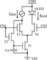
图3为本发明所述的AMOLED像素单元驱动电路的一具体实施例与OLED连接的电路图,也即本发明所述的AMOLED像素单元的一具体实施例的电路图。该实施例所述的AMOLED像素单元驱动电路采用6T1C电路,通过分流方式,使得充电电流Idata和流过OLED的电路Ioled之间具有较大的缩放比例,保证Ioled在OLED工作电流范围内,而Idata可以为较大电流,从而加快了对存储电容Cst的充电速度,解决了传统的电流型AMOLED像素因为充电电流小而产生的充电速度慢的问题。FIG. 3 is a circuit diagram of a specific embodiment of an AMOLED pixel unit driving circuit of the present invention connected to an OLED, that is, a circuit diagram of a specific embodiment of the AMOLED pixel unit of the present invention. The AMOLED pixel unit driving circuit described in this embodiment adopts a 6T1C circuit, and through the shunt mode, the charging current Idata and the circuit Ioled flowing through the OLED have a larger scaling ratio, ensuring that Ioled is within the OLED operating current range, and Idata Larger current can be used, thereby speeding up the charging speed of the storage capacitor Cst, and solving the problem of slow charging speed caused by the small charging current of the traditional current-mode AMOLED pixel.
如图3所示,T1、T2、T3、T4、T5、T6均为n型TFT,其中,T1为驱动薄膜晶体管,T2为电流分流薄膜晶体管,T3、T4、T5、T6为控制开关薄膜晶体管,Cst为存储电容,其中T1和T2的阈值电压相等。As shown in Figure 3, T1, T2, T3, T4, T5, and T6 are all n-type TFTs, wherein T1 is a driving thin film transistor, T2 is a current shunt thin film transistor, and T3, T4, T5, and T6 are control switching thin film transistors , Cst is the storage capacitor, where the threshold voltages of T1 and T2 are equal.
在图3中,T1的源极、T2的源极和Cst的第二端连接并接低电平VSS;In Figure 3, the source of T1, the source of T2 and the second end of Cst are connected and connected to the low level VSS;
T1的栅极、T2的栅极和Cst的第一端连接;The gate of T1, the gate of T2 are connected to the first end of Cst;
T1的栅极和T2的栅极通过T3与提供充电电流Idata的电流源的电流输出端连接;The gate of T1 and the gate of T2 are connected to the current output terminal of the current source that provides the charging current Idata through T3;
T1的漏极通过T4与提供充电电流Idata的电流源的电流输出端连接;The drain of T1 is connected to the current output terminal of the current source providing the charging current Idata through T4;
T2的漏极通过T6与T1的漏极连接;The drain of T2 is connected to the drain of T1 through T6;
OLED的阴极通过T5与T1的漏极连接,OLED的阳极与输出电压为VDD的电源线连接;The cathode of the OLED is connected to the drain of T1 through T5, and the anode of the OLED is connected to the power line whose output voltage is VDD;
T3、T4、T6控制在充电阶段Idata对Cst充电,T2分流;T3, T4, and T6 control Idata to charge Cst during the charging phase, and T2 shunts;
T5控制在像素充电完成后,使得驱动电流流过OLED而发光显示;T5 controls the driving current to flow through the OLED to display light after the pixel charging is completed;
T3的栅极、T4的栅极和T6的栅极连接控制信号CN1,T3的漏极、T4的漏极与提供充电电流Idata的电流源的电流输出端连接;T5的栅极连接控制信号CN2。The gate of T3, the gate of T4 and the gate of T6 are connected to the control signal CN1, the drain of T3 and T4 are connected to the current output terminal of the current source that provides the charging current Idata; the gate of T5 is connected to the control signal CN2 .
图4为控制信号CN1、控制信号CN2和充电电流Idata的时序图。FIG. 4 is a timing diagram of the control signal CN1 , the control signal CN2 and the charging current Idata.
如图5所示,该实施例所述的AMOLED像素单元驱动电路在工作时,在第一时间段,即A阶段,即像素充电阶段,CN1为高电平,CN2为低电平,T3、T4、T6导通,T5截止,存储电容Cst的第二端接地,存储电容Cst的第一端与T1和T2的公共栅极A连接,T1的源极和T2的源极连接,T1的漏极、T2的漏极与提供充电电流Idata的电流源的电流输出端连接;As shown in Figure 5, when the AMOLED pixel unit drive circuit described in this embodiment is working, in the first time period, that is, the A phase, that is, the pixel charging phase, CN1 is at a high level, CN2 is at a low level, T3, T4 and T6 are turned on, T5 is turned off, the second end of the storage capacitor Cst is grounded, the first end of the storage capacitor Cst is connected to the common gate A of T1 and T2, the source of T1 is connected to the source of T2, and the drain of T1 The drain of pole, T2 is connected with the current output end of the current source that provides charging current Idata;
在经过Idata充电后,存储电容Cst的第一端和第二端之间的电压差值为VA-VSS,此时,T1和T2处于饱和状态,流过T1的电流为Ids1,流过T2的电流为Ids2,Idata=Ids1+Ids2,T1和T2的栅源电压Vgs均为VA-VSS;After being charged by Idata, the voltage difference between the first terminal and the second terminal of the storage capacitor Cst is VA-VSS. At this time, T1 and T2 are in a saturated state, the current flowing through T1 is Ids1, and the current flowing through T2 The current is Ids2, Idata=Ids1+Ids2, the gate-source voltage Vgs of T1 and T2 are both VA-VSS;
而
因此,Ids1/Ids2=k1/k2,其中,T1与T2为沟道宽度不同的n型TFT,k1是T1的电流系数,k2是T2的电流系数;Therefore, Ids1/Ids2=k1/k2, where T1 and T2 are n-type TFTs with different channel widths, k1 is the current coefficient of T1, and k2 is the current coefficient of T2;
其中,μ1、COX、W1、L1分别为T1的场效应迁移率,栅绝缘层单位面积电容,沟道宽度、长度,μ2、COX、W2、L2分别为T2的场效应迁移率、栅绝缘层单位面积电容、沟道宽度、长度。Among them, μ1, COX , W1, and L1 are the field-effect mobility of T1, the capacitance per unit area of the gate insulating layer, channel width, and length, and μ2, COX , W2, and L2 are the field-effect mobility of T2, gate Insulation layer capacitance per unit area, channel width, length.
如图6所示,该实施例所述的AMOLED像素单元驱动电路在工作时,在第二时间段,即B阶段,即OLED发光显示阶段,CN2为高电平,CN1为高电平,T3、T4、T6截止,T5导通,存储电容Cst两端电压保持为Vgs,因此,T2截止,T1处于饱和区,所述OLED导通而发光显示;As shown in Figure 6, when the AMOLED pixel unit driving circuit described in this embodiment is working, in the second time period, that is, the B stage, that is, the OLED light-emitting display stage, CN2 is at a high level, CN1 is at a high level, and T3 , T4 and T6 are cut off, T5 is turned on, and the voltage across the storage capacitor Cst is maintained at Vgs, therefore, T2 is cut off, T1 is in the saturation region, and the OLED is turned on to display light;
此时,T1的漏电流
Ioled为流过所述OLED的电流,且
因此,Idata与Ioled的电流值的比值为(k1+k2)/k1,Ioled为电流值正比于Idata的电流值的电流,且可以使得Idata与Ioled具有较大的电流缩放比例,保证Ioled在OLED工作电流范围内,而Idata可以为较大电流,从而加快了对存储电容Cst的充电速度。Therefore, the ratio of the current value of Idata to Ioled is (k1+k2)/k1, and Ioled is a current whose current value is proportional to the current value of Idata, and can make Idata and Ioled have a larger current scaling ratio, ensuring that Ioled is in OLED Within the working current range, and Idata can be a larger current, thereby speeding up the charging speed of the storage capacitor Cst.
以上说明对本发明而言只是说明性的,而非限制性的,本领域普通技术人员理解,在不脱离所附权利要求所限定的精神和范围的情况下,可做出许多修改、变化或等效,但都将落入本发明的保护范围内。The above description is only illustrative, rather than restrictive, to the present invention. Those skilled in the art understand that many modifications, changes or the like can be made without departing from the spirit and scope defined by the appended claims. effect, but all will fall within the protection scope of the present invention.
Claims (8)
Priority Applications (3)
| Application Number | Priority Date | Filing Date | Title |
|---|---|---|---|
| CN2011102473345ACN102708787A (en) | 2011-08-25 | 2011-08-25 | Active matrix organic light emitting diode (AMOLED) pixel unit driving circuit and method, pixel unit and display device |
| PCT/CN2012/080515WO2013026404A1 (en) | 2011-08-25 | 2012-08-23 | Amoled pixel unit drive circuit and method, and pixel unit and display device |
| US13/805,732US9119259B2 (en) | 2011-08-25 | 2012-08-23 | AMOLED pixel unit driving circuit and method, AMOLED pixel unit and display apparatus |
Applications Claiming Priority (1)
| Application Number | Priority Date | Filing Date | Title |
|---|---|---|---|
| CN2011102473345ACN102708787A (en) | 2011-08-25 | 2011-08-25 | Active matrix organic light emitting diode (AMOLED) pixel unit driving circuit and method, pixel unit and display device |
Publications (1)
| Publication Number | Publication Date |
|---|---|
| CN102708787Atrue CN102708787A (en) | 2012-10-03 |
Family
ID=46901494
Family Applications (1)
| Application Number | Title | Priority Date | Filing Date |
|---|---|---|---|
| CN2011102473345APendingCN102708787A (en) | 2011-08-25 | 2011-08-25 | Active matrix organic light emitting diode (AMOLED) pixel unit driving circuit and method, pixel unit and display device |
Country Status (3)
| Country | Link |
|---|---|
| US (1) | US9119259B2 (en) |
| CN (1) | CN102708787A (en) |
| WO (1) | WO2013026404A1 (en) |
Cited By (5)
| Publication number | Priority date | Publication date | Assignee | Title |
|---|---|---|---|---|
| WO2013026404A1 (en)* | 2011-08-25 | 2013-02-28 | 京东方科技集团股份有限公司 | Amoled pixel unit drive circuit and method, and pixel unit and display device |
| CN103325338A (en)* | 2013-06-18 | 2013-09-25 | 京东方科技集团股份有限公司 | AMOLED driving circuit, AMOLED driving method and AMOLED display device |
| CN105632405A (en)* | 2016-03-18 | 2016-06-01 | 京东方科技集团股份有限公司 | Pixel drive circuit, display device and pixel driving method |
| CN106997747A (en)* | 2017-05-27 | 2017-08-01 | 京东方科技集团股份有限公司 | A kind of organic electroluminescence display panel and display device |
| WO2021035407A1 (en)* | 2019-08-23 | 2021-03-04 | 京东方科技集团股份有限公司 | Temperature compensation method for display panel, display panel, and electronic device |
Families Citing this family (1)
| Publication number | Priority date | Publication date | Assignee | Title |
|---|---|---|---|---|
| CN111968585B (en)* | 2020-08-27 | 2021-12-07 | 京东方科技集团股份有限公司 | Pixel circuit, pixel driving method and display device |
Citations (3)
| Publication number | Priority date | Publication date | Assignee | Title |
|---|---|---|---|---|
| CN1497523A (en)* | 2002-10-17 | 2004-05-19 | ������������ʽ���� | Electronic circuits, electro-optical devices and electronic instruments |
| KR20070000831A (en)* | 2005-06-28 | 2007-01-03 | 엘지.필립스 엘시디 주식회사 | Light emitting display |
| US20100097360A1 (en)* | 2008-10-16 | 2010-04-22 | Gyu-Hyeong Cho | Display driving apparatus |
Family Cites Families (27)
| Publication number | Priority date | Publication date | Assignee | Title |
|---|---|---|---|---|
| EP1130565A4 (en)* | 1999-07-14 | 2006-10-04 | Sony Corp | Current drive circuit and display comprising the same, pixel circuit, and drive method |
| US7379039B2 (en)* | 1999-07-14 | 2008-05-27 | Sony Corporation | Current drive circuit and display device using same pixel circuit, and drive method |
| KR100327374B1 (en) | 2000-03-06 | 2002-03-06 | 구자홍 | an active driving circuit for a display panel |
| JP2003005710A (en)* | 2001-06-25 | 2003-01-08 | Nec Corp | Current driving circuit and image display device |
| CN101257743B (en)* | 2001-08-29 | 2011-05-25 | 株式会社半导体能源研究所 | Light emitting device and driving method of the light emitting device |
| JP3810725B2 (en)* | 2001-09-21 | 2006-08-16 | 株式会社半導体エネルギー研究所 | LIGHT EMITTING DEVICE AND ELECTRONIC DEVICE |
| TW529006B (en) | 2001-11-28 | 2003-04-21 | Ind Tech Res Inst | Array circuit of light emitting diode display |
| JP2003295825A (en)* | 2002-02-04 | 2003-10-15 | Sanyo Electric Co Ltd | Display device |
| KR100906964B1 (en)* | 2002-09-25 | 2009-07-08 | 삼성전자주식회사 | Organic electroluminescent drive device and organic electroluminescent display panel having same |
| JP4197287B2 (en)* | 2003-03-28 | 2008-12-17 | シャープ株式会社 | Display device |
| KR100560780B1 (en)* | 2003-07-07 | 2006-03-13 | 삼성에스디아이 주식회사 | Pixel circuit of organic light emitting display device and driving method thereof |
| KR100673760B1 (en)* | 2004-09-08 | 2007-01-24 | 삼성에스디아이 주식회사 | Light emitting display |
| US7105855B2 (en)* | 2004-09-20 | 2006-09-12 | Eastman Kodak Company | Providing driving current arrangement for OLED device |
| TWI278800B (en)* | 2004-10-28 | 2007-04-11 | Au Optronics Corp | Current-driven OLED panel and related pixel structure |
| US7573444B2 (en)* | 2004-12-24 | 2009-08-11 | Samsung Mobile Display Co., Ltd. | Light emitting display |
| KR100653846B1 (en)* | 2005-04-11 | 2006-12-05 | 실리콘 디스플레이 (주) | Driving circuit and driving method of organic light emitting diode |
| KR100639007B1 (en)* | 2005-05-26 | 2006-10-25 | 삼성에스디아이 주식회사 | Light emitting display and driving method |
| US7456580B2 (en)* | 2005-06-30 | 2008-11-25 | Lg Display Co., Ltd. | Light emitting device |
| KR100666640B1 (en)* | 2005-09-15 | 2007-01-09 | 삼성에스디아이 주식회사 | Organic electroluminescent display |
| TWI338874B (en)* | 2006-03-10 | 2011-03-11 | Au Optronics Corp | Light emitting diode display and driving pixel method thereof |
| US7847767B2 (en)* | 2007-01-17 | 2010-12-07 | Himax Technologies Limited | Pixel circuit |
| US8212749B2 (en)* | 2007-03-30 | 2012-07-03 | Korea Advanced Institute Of Science And Technology | AMOLED drive circuit using transient current feedback and active matrix driving method using the same |
| JP5042329B2 (en)* | 2010-03-24 | 2012-10-03 | 株式会社沖データ | Driving device, optical print head, and image forming apparatus |
| KR101323493B1 (en)* | 2010-12-22 | 2013-10-31 | 엘지디스플레이 주식회사 | Organic light emitting diode display |
| TWI442374B (en)* | 2011-08-16 | 2014-06-21 | Hannstar Display Corp | Compensation circuit of organic light-emitting diode |
| CN102708787A (en) | 2011-08-25 | 2012-10-03 | 京东方科技集团股份有限公司 | Active matrix organic light emitting diode (AMOLED) pixel unit driving circuit and method, pixel unit and display device |
| TW201314656A (en)* | 2011-09-19 | 2013-04-01 | Chunghwa Picture Tubes Ltd | Pixel circuit and driving method thereof |
- 2011
- 2011-08-25CNCN2011102473345Apatent/CN102708787A/enactivePending
- 2012
- 2012-08-23WOPCT/CN2012/080515patent/WO2013026404A1/enactiveApplication Filing
- 2012-08-23USUS13/805,732patent/US9119259B2/enactiveActive
Patent Citations (3)
| Publication number | Priority date | Publication date | Assignee | Title |
|---|---|---|---|---|
| CN1497523A (en)* | 2002-10-17 | 2004-05-19 | ������������ʽ���� | Electronic circuits, electro-optical devices and electronic instruments |
| KR20070000831A (en)* | 2005-06-28 | 2007-01-03 | 엘지.필립스 엘시디 주식회사 | Light emitting display |
| US20100097360A1 (en)* | 2008-10-16 | 2010-04-22 | Gyu-Hyeong Cho | Display driving apparatus |
Cited By (12)
| Publication number | Priority date | Publication date | Assignee | Title |
|---|---|---|---|---|
| WO2013026404A1 (en)* | 2011-08-25 | 2013-02-28 | 京东方科技集团股份有限公司 | Amoled pixel unit drive circuit and method, and pixel unit and display device |
| US9119259B2 (en) | 2011-08-25 | 2015-08-25 | Boe Technology Group Co., Ltd. | AMOLED pixel unit driving circuit and method, AMOLED pixel unit and display apparatus |
| CN103325338A (en)* | 2013-06-18 | 2013-09-25 | 京东方科技集团股份有限公司 | AMOLED driving circuit, AMOLED driving method and AMOLED display device |
| WO2014201784A1 (en)* | 2013-06-18 | 2014-12-24 | 京东方科技集团股份有限公司 | Amoled drive circuit, drive method and display apparatus |
| CN103325338B (en)* | 2013-06-18 | 2015-06-24 | 京东方科技集团股份有限公司 | AMOLED driving circuit, AMOLED driving method and AMOLED display device |
| US9524668B2 (en) | 2013-06-18 | 2016-12-20 | Chengdu Boe Optoelectronics Technology Co., Ltd. | AMOLED driving circuit and driving method thereof, and display device |
| CN105632405A (en)* | 2016-03-18 | 2016-06-01 | 京东方科技集团股份有限公司 | Pixel drive circuit, display device and pixel driving method |
| WO2017156945A1 (en)* | 2016-03-18 | 2017-09-21 | 京东方科技集团股份有限公司 | Pixel driving circuit, display device and pixel driving method |
| CN105632405B (en)* | 2016-03-18 | 2018-09-21 | 京东方科技集团股份有限公司 | A kind of pixel-driving circuit, display equipment and image element driving method |
| US10311784B2 (en) | 2016-03-18 | 2019-06-04 | Boe Technology Group Co., Ltd. | Pixel driver circuit, display device and pixel driving method |
| CN106997747A (en)* | 2017-05-27 | 2017-08-01 | 京东方科技集团股份有限公司 | A kind of organic electroluminescence display panel and display device |
| WO2021035407A1 (en)* | 2019-08-23 | 2021-03-04 | 京东方科技集团股份有限公司 | Temperature compensation method for display panel, display panel, and electronic device |
Also Published As
| Publication number | Publication date |
|---|---|
| WO2013026404A1 (en) | 2013-02-28 |
| US9119259B2 (en) | 2015-08-25 |
| US20130147386A1 (en) | 2013-06-13 |
Similar Documents
| Publication | Publication Date | Title |
|---|---|---|
| CN102708786B (en) | Active matrix organic light emitting diode (AMOLED) pixel unit driving circuit and method, pixel unit and display device | |
| CN103971640B (en) | A kind of pixel-driving circuit and driving method thereof and display device | |
| CN103310732B (en) | Pixel circuit, driving method thereof and display device | |
| CN102708791B (en) | Pixel unit driving circuit and method, pixel unit and display device | |
| CN102708792B (en) | Pixel cell driving circuit, pixel cell driving method, pixel cell and display device | |
| CN103165080B (en) | Pixel circuit and driving method and display device thereof | |
| CN102654973B (en) | Pixel circuit, driving method thereof, and display panel | |
| CN102708798B (en) | Pixel unit driving circuit, driving method, pixel unit and display device | |
| US20150302798A1 (en) | Pixel driving circuit, display device and pixel driving method | |
| CN103500556B (en) | A kind of image element circuit and driving method, thin film transistor backplane | |
| US10283042B2 (en) | Pixel driving circuit, pixel driving method, and display device | |
| CN103325338B (en) | AMOLED driving circuit, AMOLED driving method and AMOLED display device | |
| CN103400548A (en) | Pixel driving circuit and driving method and display device thereof | |
| US20160071458A1 (en) | Led pixel unit circuit, driving method thereof, and display panel | |
| CN102789761B (en) | Pixel circuit, driving method thereof and organic light emitting display | |
| CN203288217U (en) | Pixel circuit and display device | |
| CN102708787A (en) | Active matrix organic light emitting diode (AMOLED) pixel unit driving circuit and method, pixel unit and display device | |
| CN102930821A (en) | Pixel circuit and driving method thereof and display device thereof | |
| CN102708789A (en) | Pixel unit driving circuit and method, pixel unit and display device | |
| CN101859542A (en) | Organic light emitting diode display device and organic light emitting diode pixel circuit | |
| CN104318899A (en) | Pixel unit driving circuit and method, pixel unit and display device | |
| CN102708790A (en) | Pixel unit driving circuit and method, pixel unit and display device | |
| CN102956201B (en) | Pixel circuit, driving method and display device of pixel circuit | |
| CN104078007A (en) | Active light-emitting display device pixel circuit | |
| CN102930813B (en) | Pixel-driving circuit, display device and driving method thereof |
Legal Events
| Date | Code | Title | Description |
|---|---|---|---|
| C06 | Publication | ||
| PB01 | Publication | ||
| C10 | Entry into substantive examination | ||
| SE01 | Entry into force of request for substantive examination | ||
| C12 | Rejection of a patent application after its publication | ||
| RJ01 | Rejection of invention patent application after publication | Application publication date:20121003 |