CN102707484B - Semi-transmission and semi-reflection color-film substrate and manufacturing method thereof as well as liquid crystal display device - Google Patents
Semi-transmission and semi-reflection color-film substrate and manufacturing method thereof as well as liquid crystal display deviceDownload PDFInfo
- Publication number
- CN102707484B CN102707484BCN201210122750.7ACN201210122750ACN102707484BCN 102707484 BCN102707484 BCN 102707484BCN 201210122750 ACN201210122750 ACN 201210122750ACN 102707484 BCN102707484 BCN 102707484B
- Authority
- CN
- China
- Prior art keywords
- photosensitive resin
- semi
- color filter
- layer
- reflective
- Prior art date
- Legal status (The legal status is an assumption and is not a legal conclusion. Google has not performed a legal analysis and makes no representation as to the accuracy of the status listed.)
- Expired - Fee Related
Links
Images


Classifications
- G—PHYSICS
- G02—OPTICS
- G02F—OPTICAL DEVICES OR ARRANGEMENTS FOR THE CONTROL OF LIGHT BY MODIFICATION OF THE OPTICAL PROPERTIES OF THE MEDIA OF THE ELEMENTS INVOLVED THEREIN; NON-LINEAR OPTICS; FREQUENCY-CHANGING OF LIGHT; OPTICAL LOGIC ELEMENTS; OPTICAL ANALOGUE/DIGITAL CONVERTERS
- G02F1/00—Devices or arrangements for the control of the intensity, colour, phase, polarisation or direction of light arriving from an independent light source, e.g. switching, gating or modulating; Non-linear optics
- G02F1/01—Devices or arrangements for the control of the intensity, colour, phase, polarisation or direction of light arriving from an independent light source, e.g. switching, gating or modulating; Non-linear optics for the control of the intensity, phase, polarisation or colour
- G02F1/13—Devices or arrangements for the control of the intensity, colour, phase, polarisation or direction of light arriving from an independent light source, e.g. switching, gating or modulating; Non-linear optics for the control of the intensity, phase, polarisation or colour based on liquid crystals, e.g. single liquid crystal display cells
- G02F1/133—Constructional arrangements; Operation of liquid crystal cells; Circuit arrangements
- G02F1/1333—Constructional arrangements; Manufacturing methods
- G02F1/1335—Structural association of cells with optical devices, e.g. polarisers or reflectors
- G02F1/133509—Filters, e.g. light shielding masks
- G02F1/133514—Colour filters
- G02F1/133516—Methods for their manufacture, e.g. printing, electro-deposition or photolithography
- G—PHYSICS
- G02—OPTICS
- G02B—OPTICAL ELEMENTS, SYSTEMS OR APPARATUS
- G02B5/00—Optical elements other than lenses
- G02B5/20—Filters
- G02B5/22—Absorbing filters
- G02B5/23—Photochromic filters
- G—PHYSICS
- G02—OPTICS
- G02F—OPTICAL DEVICES OR ARRANGEMENTS FOR THE CONTROL OF LIGHT BY MODIFICATION OF THE OPTICAL PROPERTIES OF THE MEDIA OF THE ELEMENTS INVOLVED THEREIN; NON-LINEAR OPTICS; FREQUENCY-CHANGING OF LIGHT; OPTICAL LOGIC ELEMENTS; OPTICAL ANALOGUE/DIGITAL CONVERTERS
- G02F1/00—Devices or arrangements for the control of the intensity, colour, phase, polarisation or direction of light arriving from an independent light source, e.g. switching, gating or modulating; Non-linear optics
- G02F1/01—Devices or arrangements for the control of the intensity, colour, phase, polarisation or direction of light arriving from an independent light source, e.g. switching, gating or modulating; Non-linear optics for the control of the intensity, phase, polarisation or colour
- G02F1/13—Devices or arrangements for the control of the intensity, colour, phase, polarisation or direction of light arriving from an independent light source, e.g. switching, gating or modulating; Non-linear optics for the control of the intensity, phase, polarisation or colour based on liquid crystals, e.g. single liquid crystal display cells
- G02F1/133—Constructional arrangements; Operation of liquid crystal cells; Circuit arrangements
- G02F1/1333—Constructional arrangements; Manufacturing methods
- G02F1/133345—Insulating layers
- G—PHYSICS
- G02—OPTICS
- G02F—OPTICAL DEVICES OR ARRANGEMENTS FOR THE CONTROL OF LIGHT BY MODIFICATION OF THE OPTICAL PROPERTIES OF THE MEDIA OF THE ELEMENTS INVOLVED THEREIN; NON-LINEAR OPTICS; FREQUENCY-CHANGING OF LIGHT; OPTICAL LOGIC ELEMENTS; OPTICAL ANALOGUE/DIGITAL CONVERTERS
- G02F1/00—Devices or arrangements for the control of the intensity, colour, phase, polarisation or direction of light arriving from an independent light source, e.g. switching, gating or modulating; Non-linear optics
- G02F1/01—Devices or arrangements for the control of the intensity, colour, phase, polarisation or direction of light arriving from an independent light source, e.g. switching, gating or modulating; Non-linear optics for the control of the intensity, phase, polarisation or colour
- G02F1/13—Devices or arrangements for the control of the intensity, colour, phase, polarisation or direction of light arriving from an independent light source, e.g. switching, gating or modulating; Non-linear optics for the control of the intensity, phase, polarisation or colour based on liquid crystals, e.g. single liquid crystal display cells
- G02F1/133—Constructional arrangements; Operation of liquid crystal cells; Circuit arrangements
- G02F1/1333—Constructional arrangements; Manufacturing methods
- G02F1/1335—Structural association of cells with optical devices, e.g. polarisers or reflectors
- G02F1/133509—Filters, e.g. light shielding masks
- G02F1/133514—Colour filters
- G—PHYSICS
- G02—OPTICS
- G02F—OPTICAL DEVICES OR ARRANGEMENTS FOR THE CONTROL OF LIGHT BY MODIFICATION OF THE OPTICAL PROPERTIES OF THE MEDIA OF THE ELEMENTS INVOLVED THEREIN; NON-LINEAR OPTICS; FREQUENCY-CHANGING OF LIGHT; OPTICAL LOGIC ELEMENTS; OPTICAL ANALOGUE/DIGITAL CONVERTERS
- G02F1/00—Devices or arrangements for the control of the intensity, colour, phase, polarisation or direction of light arriving from an independent light source, e.g. switching, gating or modulating; Non-linear optics
- G02F1/01—Devices or arrangements for the control of the intensity, colour, phase, polarisation or direction of light arriving from an independent light source, e.g. switching, gating or modulating; Non-linear optics for the control of the intensity, phase, polarisation or colour
- G02F1/13—Devices or arrangements for the control of the intensity, colour, phase, polarisation or direction of light arriving from an independent light source, e.g. switching, gating or modulating; Non-linear optics for the control of the intensity, phase, polarisation or colour based on liquid crystals, e.g. single liquid crystal display cells
- G02F1/133—Constructional arrangements; Operation of liquid crystal cells; Circuit arrangements
- G02F1/1333—Constructional arrangements; Manufacturing methods
- G02F1/1335—Structural association of cells with optical devices, e.g. polarisers or reflectors
- G02F1/133553—Reflecting elements
- G02F1/133555—Transflectors
- G—PHYSICS
- G02—OPTICS
- G02B—OPTICAL ELEMENTS, SYSTEMS OR APPARATUS
- G02B5/00—Optical elements other than lenses
- G02B5/20—Filters
- G02B5/201—Filters in the form of arrays
- G—PHYSICS
- G02—OPTICS
- G02F—OPTICAL DEVICES OR ARRANGEMENTS FOR THE CONTROL OF LIGHT BY MODIFICATION OF THE OPTICAL PROPERTIES OF THE MEDIA OF THE ELEMENTS INVOLVED THEREIN; NON-LINEAR OPTICS; FREQUENCY-CHANGING OF LIGHT; OPTICAL LOGIC ELEMENTS; OPTICAL ANALOGUE/DIGITAL CONVERTERS
- G02F1/00—Devices or arrangements for the control of the intensity, colour, phase, polarisation or direction of light arriving from an independent light source, e.g. switching, gating or modulating; Non-linear optics
- G02F1/01—Devices or arrangements for the control of the intensity, colour, phase, polarisation or direction of light arriving from an independent light source, e.g. switching, gating or modulating; Non-linear optics for the control of the intensity, phase, polarisation or colour
- G02F1/13—Devices or arrangements for the control of the intensity, colour, phase, polarisation or direction of light arriving from an independent light source, e.g. switching, gating or modulating; Non-linear optics for the control of the intensity, phase, polarisation or colour based on liquid crystals, e.g. single liquid crystal display cells
- G02F1/133—Constructional arrangements; Operation of liquid crystal cells; Circuit arrangements
- G02F1/1333—Constructional arrangements; Manufacturing methods
- G02F1/1335—Structural association of cells with optical devices, e.g. polarisers or reflectors
- G02F1/133509—Filters, e.g. light shielding masks
- G02F1/133514—Colour filters
- G02F1/133519—Overcoatings
Landscapes
- Physics & Mathematics (AREA)
- Nonlinear Science (AREA)
- General Physics & Mathematics (AREA)
- Optics & Photonics (AREA)
- Mathematical Physics (AREA)
- Chemical & Material Sciences (AREA)
- Crystallography & Structural Chemistry (AREA)
- Engineering & Computer Science (AREA)
- Manufacturing & Machinery (AREA)
- Optical Filters (AREA)
- Liquid Crystal (AREA)
Abstract
Translated fromChineseDescription
Translated fromChinese技术领域technical field
本发明涉及液晶显示器技术领域,具体可涉及一种半透射半反射彩膜基板及其制作方法,以及设置有所述半透射半反射彩膜基板的液晶显示装置。The present invention relates to the technical field of liquid crystal displays, and specifically relates to a semi-transmissive and semi-reflective color film substrate and a manufacturing method thereof, and a liquid crystal display device provided with the semi-transmissive and semi-reflective color film substrate.
背景技术Background technique
现有的液晶显示器的显示方式大体可分为透射型(Transmissive)、反射型(Reflective)和半透射半反射型(Transflective)。其中,透射型液晶显示器需要在其内部设置有背光源,当背光源产生的光线透射面板时才能使面板产生亮度,因此在室外等外界环境光较强的场景下使用透射型液晶显示器件时,难以观察透射型液晶显示器正常的显示。反射型液晶显示器是在面板的下层玻璃基板上镀反射膜,通过反射外界环境光达到显示的目的,由于没有背光源,与透射型显示器件相比,反射型液晶显示器功耗较小,但当外界环境光即光源微弱时则会引起显示品质不佳等问题。因此,兼具透射型液晶显示器和反射型液晶显示器两者功效的半透射半反射型液晶显示器引起了人们的广泛关注。在外界环境光较强时,面板反射透射进来的外界环境光来达到发光的目的,当外界环境光较弱时,面板则利用背光源来达到发光的目的,所以半透射半反射型液晶显示器具有较佳的室外辨视性与反射效果,用途更为广泛。The display modes of existing liquid crystal displays can be roughly classified into transmissive, reflective and transflective. Among them, the transmissive liquid crystal display needs to be provided with a backlight inside. When the light generated by the backlight passes through the panel, the panel can produce brightness. It is difficult to observe the normal display of the transmissive liquid crystal display. The reflective LCD is coated with a reflective film on the lower glass substrate of the panel, and achieves the purpose of display by reflecting the external ambient light. Since there is no backlight, compared with the transmissive display device, the reflective LCD consumes less power, but when When the external ambient light, that is, the light source is weak, it will cause problems such as poor display quality. Therefore, the semi-transmissive and semi-reflective liquid crystal display which has the functions of both the transmissive liquid crystal display and the reflective liquid crystal display has attracted widespread attention. When the external ambient light is strong, the panel reflects the transmitted external ambient light to achieve the purpose of emitting light; when the external ambient light is weak, the panel uses the backlight source to achieve the purpose of emitting light, so the semi-transmissive and semi-reflective liquid crystal display has Better outdoor visibility and reflection effect, more widely used.
半透射半反射彩膜基板是半透射半反射型液晶显示器中的重要器件,半透射半反射彩膜基板对于外界环境光的反射效果,直接影响了半透射半反射型液晶显示器的显示效果。The semi-transmissive and semi-reflective color film substrate is an important device in the transflective and semi-reflective liquid crystal display. The reflection effect of the transflective and semi-reflective color film substrate on the external ambient light directly affects the display effect of the transflective and semi-reflective liquid crystal display.
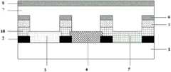
而现有半透射半反射彩膜基板结构中(已采用红、绿、蓝为原色为例),如附图1所示,通常设置有透明基板1,黑矩阵2,三种彩色滤色膜3、4、5(分别对应于红、绿、蓝三原色),反射膜6,绝缘层7(即OC层),公共电极层8(即ITO层)。而上述结构的半透射半反射彩膜基板的生产工艺需要5次掩膜曝光(mask),具体包括:首先在透明基板上涂覆黑色光阻,然后进行第一次掩膜曝光,显影后在透明基板上形成有缺口的黑矩阵(BM);随后在BM的缺口中,经过第二次掩膜曝光,制备第一型彩色滤色膜;然后以相同的方式分别进行第三、第四次掩膜曝光,在相邻的BM缺口上制备另外两种彩色滤色片;然后在彩色滤色膜和BM上溅射反射膜金属层并涂覆感光树脂即PR胶,之后经过第五次掩膜曝光、显影、湿刻后得到位于BM上具有一定图形的反射膜6。最后进行绝缘层7和公共电极层8的制作。In the existing semi-transmissive and semi-reflective color film substrate structure (red, green, and blue have been used as primary colors as an example), as shown in Figure 1, a
附图1为现有工艺制造的半透半反型彩膜基板的剖面图。Accompanying
在现有的半透射半反射彩膜基板的生产工艺中所涉及的五次曝光均从彩膜基板的正面(彩膜基板设置有彩色滤色膜的一面,即彩膜基板的顶部方向)进行,而且都需使用特定的掩模板(mask)进行曝光,该过程中需要对彩膜基板进行精确对准,一旦掩模板相对于彩膜基板的偏移超过一个微小的数值,则会使得上下两层图形不匹配,导致面板(panel)出现漏光、显示异常等较为严重的问题,从而导致现有的半透射半反射彩膜基板的生产工艺较为复杂。The five exposures involved in the production process of the existing semi-transmissive and semi-reflective color filter substrates are all carried out from the front of the color filter substrate (the side of the color filter substrate with the color filter film, that is, the top direction of the color filter substrate) , and all need to use a specific mask for exposure. In this process, the color filter substrate needs to be precisely aligned. Once the offset of the mask relative to the color filter substrate exceeds a small value, it will make the upper and lower sides Layer patterns do not match, leading to relatively serious problems such as light leakage and abnormal display on the panel, which leads to a relatively complicated production process of the existing semi-transmissive and semi-reflective color film substrate.
发明内容Contents of the invention
本发明为了解决现有半透射半反射彩膜基板的生产工艺较为复杂的技术问题,提供一种半透射半反射彩膜基板及其制作方法,以及液晶显示装置,从而简化了半透射半反射彩膜基板的生产工艺。In order to solve the technical problem that the production process of the existing semi-transmissive and semi-reflective color film substrate is relatively complicated, the present invention provides a semi-transmissive and semi-reflective color film substrate and its manufacturing method, as well as a liquid crystal display device, thereby simplifying the transflective and semi-reflective color film substrate. The production process of the film substrate.
本发明提供方案如下:The present invention provides scheme as follows:
本发明实施例提供了一种半透射半反射彩膜基板,所述彩膜基板包括一透明基板,设置于所述透明基板之上的黑矩阵,以及设置于所述黑矩阵的缺口中用于呈现不同原色的多个彩色滤色片;An embodiment of the present invention provides a semi-transmissive and semi-reflective color filter substrate. The color filter substrate includes a transparent substrate, a black matrix arranged on the transparent substrate, and a black matrix arranged in a gap of the black matrix for Multiple color filters representing different primary colors;
所述多个彩色滤色片中的第一彩色滤色片的材质为负性光敏树脂,其他彩色滤色片的材质为正性光敏树脂。The material of the first color filter among the plurality of color filters is negative photosensitive resin, and the material of other color filters is positive photosensitive resin.
优选的,所述的半透射半反射彩膜基板还包括:Preferably, the semi-transmissive and semi-reflective color filter substrate further includes:
设置于所述黑矩阵上的负性光敏树脂层,所述负性光敏树脂层的材质与第一彩色滤色片的材质相同;A negative photosensitive resin layer disposed on the black matrix, the material of the negative photosensitive resin layer is the same as that of the first color filter;
设置于所述负性光敏树脂层上的正性光敏树脂层;a positive photosensitive resin layer disposed on the negative photosensitive resin layer;
设置于所述正性光敏树脂层上的反射膜层。A reflective film layer arranged on the positive photosensitive resin layer.
优选的,所述的半透射半反射彩膜基板还包括:Preferably, the semi-transmissive and semi-reflective color filter substrate further includes:
设置于所述反射膜层以及彩色滤色片上的绝缘层;An insulating layer disposed on the reflective film layer and the color filter;
设置于所述绝缘层上的公共电极层。A common electrode layer arranged on the insulating layer.
本发明实施例还提供了一种半透射半反射彩膜基板制作方法,该方法用于制作上述本发明实施例提供的半透射半反射彩膜基板;The embodiment of the present invention also provides a method for manufacturing a semi-transmissive and semi-reflective color film substrate, which is used to manufacture the above-mentioned semi-transmissive and semi-reflective color film substrate provided by the above-mentioned embodiments of the present invention;
所述方法包括:The methods include:
在透明基板已经生成的黑矩阵、其他彩色滤色片以及黑矩阵缺口上,涂覆一层负性光敏树脂,生成负性光敏树脂层,在所述负性光敏树脂层上涂覆一层正性光敏树脂,生成正性光敏树脂层,在所述正性光敏树脂层上生成反射膜层,所述其他彩色滤色片为材质是正性光敏树脂的彩色滤色片;On the black matrix, other color filters and black matrix gaps that have been generated on the transparent substrate, a layer of negative photosensitive resin is coated to form a negative photosensitive resin layer, and a layer of positive photosensitive resin is coated on the negative photosensitive resin layer. positive photosensitive resin to generate a positive photosensitive resin layer, a reflective film layer is generated on the positive photosensitive resin layer, and the other color filters are color filters made of positive photosensitive resin;
从透明基板的底部方向进行背向曝光;Back exposure from the bottom direction of the transparent substrate;
对曝光后的正性光敏树脂层进行显影处理,移除其他彩色滤色片以及第一彩色滤色片对应位置上方的正性光敏树脂层以及反射膜层,露出其他彩色滤色片以及第一彩色滤色片对应位置上方的所述负性光敏树脂层;After exposure, the positive photosensitive resin layer is developed, and the positive photosensitive resin layer and the reflective film layer above the corresponding positions of other color filters and the first color filter are removed to expose other color filters and the first color filter. The negative photosensitive resin layer above the corresponding position of the color filter;
对其他彩色滤色片以及第一彩色滤色片对应位置上方的负性光敏树脂层进行灰化处理,移除覆盖在其他彩色滤色片上的负性光敏树脂层,并生成第一彩色滤色片。Ashing the negative photosensitive resin layer above the corresponding positions of other color filters and the first color filter, removing the negative photosensitive resin layer covering other color filters, and generating the first color filter piece.
优选的,在透明基板已经生成的黑矩阵、其他彩色滤色片以及黑矩阵缺口上,涂覆一层负性光敏树脂,生成负性光敏树脂层之前,所述方法还包括:Preferably, on the black matrix that has been generated on the transparent substrate, other color filters and black matrix gaps, a layer of negative photosensitive resin is coated, and before the negative photosensitive resin layer is generated, the method also includes:
在透明基板上涂覆一层黑色光阻;Coating a layer of black photoresist on the transparent substrate;
从所述透明基板的顶部方向,对于所述黑色光阻进行正向掩膜曝光,并对曝光后的黑色光阻进行显影处理,生成具有缺口的黑矩阵。From the top direction of the transparent substrate, the black photoresist is subjected to positive mask exposure, and the exposed black photoresist is developed to generate a black matrix with gaps.
优选的,在透明基板已经生成的黑矩阵、其他彩色滤色片以及黑矩阵缺口上,涂覆一层负性光敏树脂,生成负性光敏树脂层之前,所述方法还包括:Preferably, on the black matrix that has been generated on the transparent substrate, other color filters and black matrix gaps, a layer of negative photosensitive resin is coated, and before the negative photosensitive resin layer is generated, the method also includes:
在生成的黑矩阵的缺口处,经过正向掩膜曝光,依次生成材质为正性光敏树脂的其他彩色滤色片,且此步骤中所述正向掩膜曝光次数与其他彩色滤色片所呈现的原色种类数目对应。At the gap of the generated black matrix, through the forward mask exposure, other color filters that are made of positive photosensitive resin are sequentially generated, and the number of positive mask exposures described in this step is the same as that of other color filters. Corresponds to the number of primary color types presented.
优选的,在生成第一彩色滤色片之后,所述方法还包括:Preferably, after generating the first color filter, the method further includes:
在彩色滤色片以及剩余反射膜层上生成绝缘层;Generate an insulating layer on the color filter and the remaining reflective film layer;
在所述绝缘层生成公共电极层。A common electrode layer is formed on the insulating layer.
本发明实施例还提供了一种液晶显示装置,该液晶显示装置包括一半透射半反射液晶显示面板;所述半透射半反射液晶显示面板包括如权利要求1至3任一项所述的半透射半反射彩膜基板。The embodiment of the present invention also provides a liquid crystal display device, the liquid crystal display device comprises a semi-transmissive and semi-reflective liquid crystal display panel; Semi-reflective color film substrate.
从以上所述可以看出,本发明提供的一种半透射半反射彩膜基板及其制作方法,以及一种液晶显示装置,该半透射半反射彩膜基板在设置于透明基板上的黑矩阵的缺口中,设置有用于呈现不同原色的多个彩色滤色片,其中通过从透明基板底部方向进行背向曝光而最后制作生成的第一彩色滤色片的材质为负性光敏树脂,在第一彩色滤色片之前通过从透明基板顶部方向进行正向掩膜曝光生成的其他彩色滤色片的材质为正性光敏树脂,从而通过一次背向曝光实现现有技术中需要两次正向掩膜曝光才能生成的图层,使得半透射半反射彩膜基板的生产工艺得以简化,并有效的提高了产品优良率。It can be seen from the above that the present invention provides a semi-transmissive and semi-reflective color filter substrate and a manufacturing method thereof, as well as a liquid crystal display device. A plurality of color filters for displaying different primary colors are arranged in the gap of the transparent substrate, wherein the material of the first color filter produced by back exposure from the bottom direction of the transparent substrate is a negative photosensitive resin. A color filter is made of positive photosensitive resin through positive mask exposure from the top direction of the transparent substrate, so that two forward masks are required in the prior art through one back exposure. The layer that can only be generated by film exposure simplifies the production process of the semi-transmissive and semi-reflective color film substrate, and effectively improves the product quality rate.
附图说明Description of drawings
图1为现有工艺制造的半透半反型彩膜基板的剖面图;FIG. 1 is a cross-sectional view of a transflective color filter substrate manufactured by an existing process;
图2为本发明实施例提供的半透半反型彩膜基板的剖面图;Fig. 2 is a cross-sectional view of a transflective color filter substrate provided by an embodiment of the present invention;
图3本发明实施例提供的半透半反型彩膜基板制作方法流程示意图;Fig. 3 is a schematic flow chart of the manufacturing method of the semi-transparent and semi-reflective color filter substrate provided by the embodiment of the present invention;
图4本发明实施例提供的半透半反型彩膜基板制作方法具体实现过程示意图一;Fig. 4 is a schematic diagram of the specific implementation process of the manufacturing method of the semi-transparent and semi-reflective color filter substrate provided by the embodiment of the present invention;
图5本发明实施例提供的半透半反型彩膜基板制作方法具体实现过程示意图二;Fig. 5 is a schematic diagram of the specific implementation process of the manufacturing method of the semi-transparent and semi-reflective color filter substrate provided by the embodiment of the present invention;
图6本发明实施例提供的半透半反型彩膜基板制作方法具体实现过程示意图三;Fig. 6 is a schematic diagram of the specific implementation process of the manufacturing method of the semi-transparent and semi-reflective color filter substrate provided by the embodiment of the present invention;
图7本发明实施例提供的半透半反型彩膜基板制作方法具体实现过程示意图四;Fig. 7 is a schematic diagram of the specific implementation process of the manufacturing method of the semi-transparent and semi-reflective color filter substrate provided by the embodiment of the present invention;
图8本发明实施例提供的半透半反型彩膜基板制作方法具体实现过程示意图五;Fig. 8 is a schematic diagram of the specific implementation process of the manufacturing method of the semi-transparent and semi-reflective color filter substrate provided by the embodiment of the present invention;
图9本发明实施例提供的半透半反型彩膜基板制作方法具体实现过程示意图六;Fig. 9 is a schematic diagram of the specific implementation process of the manufacturing method of the semi-transparent and semi-reflective color filter substrate provided by the embodiment of the present invention;
图10发明实施例提供的半透半反型彩膜基板制作方法具体实现过程示意图七;Fig. 10 is a schematic diagram of the specific implementation process of the manufacturing method of the semi-transparent and semi-reflective color filter substrate provided by the embodiment of the invention;
图11发明实施例提供的半透半反型彩膜基板制作方法具体实现过程示意图八;Fig. 11 is a schematic diagram of the specific implementation process of the manufacturing method of the semi-transparent and semi-reflective color filter substrate provided by the embodiment of the invention;
图12发明实施例提供的半透半反型彩膜基板制作方法具体实现过程示意图九;Figure 12 is a schematic diagram of the specific implementation process of the manufacturing method of the semi-transparent and semi-reflective color filter substrate provided by the embodiment of the invention;
图13发明实施例提供的半透半反型彩膜基板制作方法具体实现过程示意图十;Figure 13 is a schematic diagram of the specific implementation process of the manufacturing method of the semi-transparent and semi-reflective color filter substrate provided by the embodiment of the invention;
图14发明实施例提供的半透半反型彩膜基板制作方法具体实现过程示意图十一。Fig. 14 is a schematic diagram of the specific implementation process of the manufacturing method of the transflective and transflective color filter substrate provided by the embodiment of the invention.
具体实施方式Detailed ways
本发明实施例提供了一种半透射半反射彩膜基板,如附图2示,该彩膜基板具体可以包括一透明基板1;An embodiment of the present invention provides a semi-transmissive and semi-reflective color filter substrate, as shown in Figure 2, the color filter substrate may specifically include a
设置于所述透明基板之上的黑矩阵2;a
设置于黑矩阵2缺口中,用于呈现不同原色的多个彩色滤色片,其中,通过从透明基板底部方向进行背向曝光而最后制作生成的第一彩色滤色片5的材质为负性光敏树脂,而在所述第一彩色滤色片之前通过从透明基板顶部方向进行正向掩膜曝光生成的其他彩色滤色片(包括彩色滤色3以及彩色滤色片4)的材质为正性光敏树脂。It is arranged in the gap of the
该半透射半反射彩膜基板具体还可以包括:Specifically, the semi-transmissive and semi-reflective color filter substrate may further include:
设置于黑矩阵2上的负性光敏树脂层10;A negative
设置于负性光敏树脂层10上的正性光敏树脂层9;A positive
设置于正性光敏树脂层9上的反射膜层6。The
另外,该半透射半反射彩膜基板具体还可以包括:In addition, the semi-transmissive and semi-reflective color filter substrate may further include:
设置于反射膜层6以及彩色滤色片上的绝缘层7;An insulating
设置于绝缘层7上的公共电极层8。A
这里需要说明的是,附图2所示的半透射半反射彩膜基板,仅为举例说明,其中所涉及的原色具体可为三原色(如红、绿、蓝),分别由图2中所示的彩色滤色片3、彩色滤色片4、彩色滤色片5呈现对应的颜色。但这并不表示本发明实施例中仅包括三种彩色滤色片,随着技术的发展,本发明实施例提供的半透射半反射彩膜基板中,还可包括分别对应于四原色、五原色的四种、五种彩色滤色片等。It should be noted here that the semi-transmissive and semi-reflective color filter substrate shown in Figure 2 is only an example, and the primary colors involved can specifically be three primary colors (such as red, green, and blue), which are respectively shown in Figure 2. The
进一步说明的是,无论是三种彩色滤色片,还是四种彩色滤色片,本发明实施例所涉及的第一彩色滤色片均为最后制作生成的彩色滤色片(材质负性光敏树脂),而其他彩色滤色片则为第一彩色滤色片之前生成的彩色滤色片(材质为正性光敏树脂)。It is further explained that, whether it is three kinds of color filters or four kinds of color filters, the first color filter involved in the embodiment of the present invention is the last produced color filter (material negative photosensitive resin), while the other color filters are the color filters produced before the first color filter (the material is positive photosensitive resin).
而且,本发明实施例提供的半透半反彩膜基板,主要是对现有半透半反彩膜基板的结构、材质以及制作工艺进行改进,对彩膜基板的功能并不会造成影响。Moreover, the transflective color filter substrate provided by the embodiment of the present invention mainly improves the structure, material and manufacturing process of the existing transflective color filter substrate without affecting the function of the color filter substrate.
为了制作如附图2所示的半透射半反射彩膜基板,本发明实施例还提供了一种半透射半反射彩膜基板制作方法,如附图3所示,所述方法包括:In order to manufacture the semi-transmissive and semi-reflective color film substrate as shown in Figure 2, an embodiment of the present invention also provides a method for manufacturing a semi-transmissive and semi-reflective color film substrate, as shown in Figure 3, the method includes:
步骤31,在透明基板1已经生成的黑矩阵2、其他彩色滤色片(3、4)以及黑矩阵缺口上,涂覆一层负性光敏树脂,生成负性光敏树脂层10,在所述负性光敏树脂层10上涂覆一层正性光敏树脂,生成正性光敏树脂层9,在所述正性光敏树脂层9上生成反射膜层6,所述其他彩色滤色片为材质是正性光敏树脂的彩色滤色片;
步骤32,从透明基板1的底部方向进行背向曝光;
步骤33,对曝光后的正性光敏树脂层9进行显影处理,移除其他彩色滤色片(3、4)以及第一彩色滤色片5对应位置上方的正性光敏树脂层9以及反射膜层6,露出其他彩色滤色片(3、4)以及第一彩色滤色片5对应位置上方的负性光敏树脂层10;
步骤34,对其他彩色滤色片(3、4)以及第一彩色滤色片5对应位置上的负性光敏树脂层10进行灰化处理,移除覆盖在其他彩色滤色片(3、4)上的负性光敏树脂层10,并生成第一彩色滤色片5。
本发明实施例提供的半透射半反射彩膜基板制作方法,通过一次背向曝光即可实现现有技术中需要两次正向掩膜曝光才能生成的图层,使得半透射半反射彩膜基板的生产工艺得以简化,并且,本发明实施例中所涉及的背向曝光,使用透明基板1上已经生成的图形作为掩膜板,是一种自对准曝光,从而确保了背向曝光的精度,有效的提高了产品优良率。The manufacturing method of the semi-transmissive and semi-reflective color film substrate provided by the embodiment of the present invention can realize the layer that needs two forward mask exposures in the prior art to be generated by one back exposure, so that the semi-transmissive and semi-reflective color film substrate The production process is simplified, and the back exposure involved in the embodiment of the present invention uses the pattern that has been generated on the
另外,本发明实施例提供的半透射半反射彩膜基板制作方法,在透明基板1已经生成的黑矩阵2、其他彩色滤色片(3、4)以及黑矩阵缺口上,涂覆一层负性光敏树脂,生成负性光敏树脂层10之前还包括:In addition, in the manufacturing method of the semi-transmissive and semi-reflective color filter substrate provided by the embodiment of the present invention, a negative layer is coated on the
在透明基板1上涂覆一层黑色光阻;coating a layer of black photoresist on the
从透明基板1的顶部方向,对于所述黑色光阻进行正向掩膜曝光,并对曝光后的黑色光阻进行显影处理,生成具有缺口的黑矩阵2。From the top direction of the
另外,本发明实施例提供的半透射半反射彩膜基板制作方法,在透明基板1已经生成的黑矩阵2、其他彩色滤色片(3、4)以及黑矩阵缺口上,涂覆一层负性光敏树脂,生成负性光敏树脂层10之前还包括:In addition, in the manufacturing method of the semi-transmissive and semi-reflective color filter substrate provided by the embodiment of the present invention, a negative layer is coated on the
在生成的黑矩阵2的缺口处,经过正向掩膜曝光,依次生成材质为正性光敏树脂的其他彩色滤色片(3、4),且此步骤中所述正向掩膜曝光次数与其他彩色滤色片所呈现的原色种类对应。例如,当需要制作红色对应的彩色滤色片时,需要进行一次正向掩膜曝光;当需要制作绿色对应的彩色滤色片时,需要再进行一次正向掩膜曝光,依此类推,直到完成全部其他彩色滤色片的制作。At the gap of the generated
另外,本发明实施例提供的半透射半反射彩膜基板制作方法,在生成第一彩色滤色片之后还包括:In addition, the method for manufacturing a semi-transmissive and semi-reflective color filter substrate provided in an embodiment of the present invention further includes after generating the first color filter:
在彩色滤色片以及剩余反射膜层6上生成绝缘层7;Generating an insulating
在所述绝缘层7生成公共电极层8。A
为了便于对本发明实施例提供的半透射半反射彩膜基板制作方法的理解,下面结合附图,对该方法的一个具体实施例的实现过程进行详尽的表述。In order to facilitate the understanding of the manufacturing method of the semi-transmissive and semi-reflective color filter substrate provided by the embodiment of the present invention, the implementation process of a specific embodiment of the method will be described in detail below with reference to the accompanying drawings.
此实施例中,该方法用于制作一包含与三原色对应的三种彩色滤色片(即如附图2所示的彩色滤色片3、彩色滤色片4、彩色滤色片5)的半透射半反射彩膜基板。In this embodiment, the method is used to make a color filter that includes three kinds of color filters corresponding to the three primary colors (i.e.
该实施例具体可以包括:This embodiment can specifically include:
步骤1、在透明基板1上进行黑矩阵的制备。
本发明实施例中,黑矩阵BM的制备工艺可与现有技术相同,如附图4所示,即先在透明基板1上涂覆一层黑色光阻,然后黑色光阻进行一次正向掩膜曝光,即从透明基板1的顶部方向,对于透明基板1进行第一次正向掩膜曝光,并对曝光后的黑色光阻进行显影处理,生成如附图5所示的,具有缺口的黑矩阵2即BM层2。In the embodiment of the present invention, the preparation process of the black matrix BM can be the same as that of the prior art, as shown in FIG. Film exposure, that is, from the direction of the top of the
步骤2、制作彩色滤色片3、4。
该过程可与现有技术相同,即在已经生成黑矩阵2的透明基板1上,涂覆一层正性光敏树脂,如附图6所示。This process can be the same as the prior art, that is, a layer of positive photosensitive resin is coated on the
然后对涂覆后的正性光敏树脂层(需要说明的是,此次曝光的正性光敏树脂层并不是彩膜基板中所设置的正性光敏树脂层9)进行一次正向掩膜曝光,即从透明基板1的顶部方向,进行第二次正向掩膜曝光,生成如附图7所示的、材质为正性光敏树脂的彩色滤色片3。Then the positive photosensitive resin layer after coating (it should be noted that the positive photosensitive resin layer exposed this time is not the positive
然后以相同的制备过程,即经过第三次正向掩膜曝光,生成材质同样为正性光敏树脂的彩色滤色片4。该过程具体可如附图8、9所示。Then, by the same preparation process, that is, through the third forward mask exposure, the
步骤3、制作负性光敏树脂层10、正性光敏树脂层9、反射膜层6以及彩色滤色片5。
本实施例中,彩色滤色片5的制备工艺与现有技术不同,是本发明的技术贡献之一。In this embodiment, the manufacturing process of the
该工艺具体包括:The process specifically includes:
首先,在透明基板1上涂覆一层负性光敏树脂,其厚度略大于其他两种彩色滤色片。First, a layer of negative photosensitive resin is coated on the
然后,将负性光敏树脂上表面刮平,形成负性光敏树脂层10。Then, the upper surface of the negative photosensitive resin is scraped to form the negative
此时的彩膜基板可如附图10所示。The color filter substrate at this time can be as shown in FIG. 10 .
接下来,直接在负性光敏树脂层10上涂覆一层正性光敏树脂即光刻胶,形成正性光敏树脂层9。Next, a layer of positive photosensitive resin, namely photoresist, is directly coated on the negative
然后,在正性光敏树脂层9上溅射生成反射膜层6。Then, the
此时的彩膜基板可如附图11所示。The color filter substrate at this time can be as shown in FIG. 11 .
本发明实施例中,反射膜层6所适用的金属材料具体可以是铝(Al)、银(Ag)、金(Au)及其合金材料,也可以是其他反射性能较好的金属或合金,比如:金属铂(Pt)、铬(Cr)、铜(Cu)等。In the embodiment of the present invention, the metal material suitable for the
在负性光敏树脂层10、正性光敏树脂层9以及反射膜层6这三层薄膜沉积完成后,从透明基板1的底部即下方,进行背向曝光。After the deposition of the three thin films of the negative
该背向曝光不需要使用掩模板,直接以基板上已有的BM 2和彩色滤色片3、4的图形为掩膜板,自对准进行曝光。其中BM是不透光的,而彩色滤色片3、4是可以透光的。该过程如附图12所示。The back exposure does not need to use a mask, and directly uses the existing patterns of
曝光完成后,采用正性光刻胶的显影液对透明基板1进行显影处理,即移除图形化后彩色滤色片3、4和彩色滤色片5对应位置上方的被曝光的正性光敏树脂层9,并且因为被曝光的正性光敏树脂层9被移除,一并剥离位于其上的反射膜层6,从而形成如附图13所示的彩膜基板。After the exposure is completed, the
从附图13可以看出,部分负性光敏树脂层10即彩色滤色片3、4和彩色滤色片5对应位置上方的负性光敏树脂层10已经暴露出来。It can be seen from FIG. 13 that part of the negative
那么,接下来可以对暴漏出来的负性光敏树脂层10进行灰化,移除覆盖在彩色滤色片3、4上的负性光敏树脂层,从而露出材质为正性光敏树脂的彩色滤色片3、4。Then, the exposed negative
同时,还可以对彩色滤色片5对应位置上方的负性光敏树脂层10进行灰化,从而生成材质为负性光敏树脂的彩色滤色片5。At the same time, the negative
此段工艺完成后就得到了BM与三种彩色滤色片交替排列,并且BM上覆盖了反射膜层6的彩膜基板,具体可如附图14所示。After this process is completed, the BM and the three kinds of color filters are alternately arranged, and the color filter substrate is covered with the
步骤4,依照传统技术在基板上涂覆绝缘OC层7,溅射公共电极ITO层8。最终得到了如附图2所示的,半透射半反射彩膜基板。
通过上述描述可以看出,本发明实施例提出的半透射半反射彩膜基板制作方法,是一种全新的生产工艺,该工艺过程中,总共需要三次掩膜曝光和一次自对准曝光,相比起现有技术的5次掩膜曝光(仅对应于包括三种彩色滤色片),减少了一次曝光工艺,工艺难度大大降低,工艺过程也得到了减少,有效地提高了产品良率,有利于生产成本的降低。It can be seen from the above description that the semi-transmissive and semi-reflective color film substrate manufacturing method proposed in the embodiment of the present invention is a brand-new production process. In this process, a total of three mask exposures and one self-alignment exposure are required. Compared with the five mask exposures in the prior art (corresponding to only including three color filters), one exposure process is reduced, the process difficulty is greatly reduced, and the process is also reduced, effectively improving the product yield. Conducive to the reduction of production costs.
并且,从背面对透明基板1进行曝光时,可以使用透明基板1上已经生成的图形作为掩膜板,进行自对准曝光,减少了一次掩模板的对位,也就是说,整个工艺过程仅需进行三次掩膜板的对准,和一次简单的自对准曝光即可,大大简化了半透半反彩膜基板的制造工艺。Moreover, when exposing the
基于按照本发明实施例提供的半透射半反射彩膜基板制作方法而制作生成的半透射半反射彩膜基板,本发明实施例还可以提供一种液晶显示装置,该液晶显示器具体可以包括一半透射半反射液晶显示面板。Based on the semi-transmissive and semi-reflective color film substrate produced by the semi-transmissive and semi-reflective color film substrate manufacturing method according to the embodiment of the present invention, the embodiment of the present invention can also provide a liquid crystal display device, and the liquid crystal display can specifically include a semi-transmissive and semi-reflective color film substrate. Semi-reflective LCD panel.
该半透射半反射液晶显示面板具体可以包括:The transflective liquid crystal display panel may specifically include:
阵列基板,如图2所示的半透射半反射彩膜基板,以及设置于所述半透射半反射彩膜基板与阵列基板之间的液晶层。The array substrate is a transflective and semireflective color filter substrate as shown in FIG. 2 , and a liquid crystal layer disposed between the transflective and semireflective color filter substrate and the array substrate.
另外,本发明实施例还可以提供一种电子产品,该电子产品中包括本发明实施例提供的液晶显示装置,该液晶显示装置中包括如附图2所示的半透射半反射彩膜基板。In addition, the embodiment of the present invention can also provide an electronic product, the electronic product includes the liquid crystal display device provided by the embodiment of the present invention, and the liquid crystal display device includes the semi-transmissive and semi-reflective color filter substrate as shown in Fig. 2 .
以上所述仅是本发明的实施方式,应当指出,对于本技术领域的普通技术人员来说,在不脱离本发明原理的前提下,还可以作出若干改进和润饰,这些改进和润饰也应视为本发明的保护范围。The above is only the embodiment of the present invention, it should be pointed out that for those of ordinary skill in the art, without departing from the principle of the present invention, some improvements and modifications can also be made, and these improvements and modifications should also be regarded as Be the protection scope of the present invention.
Claims (8)
Translated fromChinesePriority Applications (3)
| Application Number | Priority Date | Filing Date | Title |
|---|---|---|---|
| CN201210122750.7ACN102707484B (en) | 2012-04-24 | 2012-04-24 | Semi-transmission and semi-reflection color-film substrate and manufacturing method thereof as well as liquid crystal display device |
| US14/127,299US9360700B2 (en) | 2012-04-24 | 2012-12-07 | Half-transmitting and half-reflecting color film substrate, manufacture method thereof and liquid crystal display device |
| PCT/CN2012/086196WO2013159537A1 (en) | 2012-04-24 | 2012-12-07 | Half-transmitting and half-reflecting color film substrate, manufacture method thereof and liquid crystal display device |
Applications Claiming Priority (1)
| Application Number | Priority Date | Filing Date | Title |
|---|---|---|---|
| CN201210122750.7ACN102707484B (en) | 2012-04-24 | 2012-04-24 | Semi-transmission and semi-reflection color-film substrate and manufacturing method thereof as well as liquid crystal display device |
Publications (2)
| Publication Number | Publication Date |
|---|---|
| CN102707484A CN102707484A (en) | 2012-10-03 |
| CN102707484Btrue CN102707484B (en) | 2014-07-09 |
Family
ID=46900396
Family Applications (1)
| Application Number | Title | Priority Date | Filing Date |
|---|---|---|---|
| CN201210122750.7AExpired - Fee RelatedCN102707484B (en) | 2012-04-24 | 2012-04-24 | Semi-transmission and semi-reflection color-film substrate and manufacturing method thereof as well as liquid crystal display device |
Country Status (3)
| Country | Link |
|---|---|
| US (1) | US9360700B2 (en) |
| CN (1) | CN102707484B (en) |
| WO (1) | WO2013159537A1 (en) |
Families Citing this family (22)
| Publication number | Priority date | Publication date | Assignee | Title |
|---|---|---|---|---|
| CN102707484B (en) | 2012-04-24 | 2014-07-09 | 京东方科技集团股份有限公司 | Semi-transmission and semi-reflection color-film substrate and manufacturing method thereof as well as liquid crystal display device |
| CN103033981B (en)* | 2013-01-09 | 2016-05-11 | 深圳市华星光电技术有限公司 | Colored filter substrate and manufacture method thereof and liquid crystal panel |
| CN103325732B (en) | 2013-06-28 | 2016-03-30 | 京东方科技集团股份有限公司 | A kind of COA substrate and manufacture method, display unit |
| CN103760717A (en)* | 2014-01-29 | 2014-04-30 | 京东方科技集团股份有限公司 | Color filter substrate, preparation method thereof and display device, |
| TWI557772B (en)* | 2014-04-10 | 2016-11-11 | 友達光電股份有限公司 | Device substrate and fabricating method thereof |
| CN104156130B (en)* | 2014-07-17 | 2019-02-05 | 重庆京东方光电科技有限公司 | A touch screen and display device |
| CN104156131B (en)* | 2014-08-20 | 2017-07-28 | 深圳市华星光电技术有限公司 | The manufacture method of touch-screen |
| CN104360428B (en)* | 2014-11-28 | 2016-08-24 | 京东方科技集团股份有限公司 | Make method and colored filter, the display device of colored filter |
| CN104571716B (en)* | 2015-02-03 | 2017-08-29 | 京东方科技集团股份有限公司 | Upper substrate and preparation method, touch-control display panel and preparation method |
| CN105118928B (en)* | 2015-07-29 | 2018-02-09 | 京东方科技集团股份有限公司 | Color membrane substrates, its preparation method, OLED display panel and display device |
| US10996515B2 (en)* | 2015-08-28 | 2021-05-04 | Samsung Display Co., Ltd. | Color conversion panel, display device comprising the same and manufacturing method of the color conversion panel |
| CN205942207U (en)* | 2016-05-17 | 2017-02-08 | 京东方科技集团股份有限公司 | Display panel and display device |
| CN106019708A (en)* | 2016-07-15 | 2016-10-12 | 京东方科技集团股份有限公司 | Backlight module and transparent display device including backlight module |
| CN106226945A (en)* | 2016-07-29 | 2016-12-14 | 信利(惠州)智能显示有限公司 | Colored filter and preparation method thereof, display module and display device |
| CN107065292A (en)* | 2017-06-12 | 2017-08-18 | 京东方科技集团股份有限公司 | Black matrix and preparation method thereof and system, display base plate and display device |
| KR102454192B1 (en)* | 2017-07-19 | 2022-10-13 | 삼성디스플레이 주식회사 | Color conversion panel and display device including the same |
| CN110412790A (en) | 2018-04-26 | 2019-11-05 | 京东方科技集团股份有限公司 | Color filter substrate, display panel, display device, and display device operating method |
| KR102432033B1 (en)* | 2018-07-05 | 2022-08-12 | 도레이 카부시키가이샤 | Resin composition, light-shielding film, manufacturing method of light-shielding film, and substrate with barrier ribs |
| CN110858035B (en)* | 2018-08-24 | 2022-12-02 | 夏普株式会社 | Liquid crystal display device |
| CN111724816B (en)* | 2019-03-20 | 2023-09-22 | 新科实业有限公司 | Method of forming a pattern on a substrate |
| CN110224076B (en)* | 2019-05-15 | 2020-08-11 | 武汉华星光电半导体显示技术有限公司 | OLED panel and manufacturing method thereof |
| US12321059B2 (en)* | 2023-07-11 | 2025-06-03 | Dell Products L.P. | Display panel with reduced reflectance |
Citations (3)
| Publication number | Priority date | Publication date | Assignee | Title |
|---|---|---|---|---|
| CN1773314A (en)* | 2004-11-11 | 2006-05-17 | Lg.菲利浦Lcd株式会社 | Thin film patterning device and method for manufacturing color filter array substrate using same |
| CN1975544A (en)* | 2006-12-06 | 2007-06-06 | 友达光电股份有限公司 | Method for producing liquid crystal display device substrate |
| JP2008242284A (en)* | 2007-03-28 | 2008-10-09 | Dainippon Printing Co Ltd | Manufacturing method of color filter for transflective liquid crystal display device |
Family Cites Families (9)
| Publication number | Priority date | Publication date | Assignee | Title |
|---|---|---|---|---|
| WO2004046801A1 (en)* | 2002-11-15 | 2004-06-03 | Seiko Instruments Inc. | Liquid crystal display unit |
| JP2004218123A (en) | 2003-01-14 | 2004-08-05 | Teijin Ltd | Method for producing conjugate fiber, the resultant conjugate fiber, and nonwoven fabric comprising the same |
| JP4749678B2 (en)* | 2003-04-30 | 2011-08-17 | サムスン エレクトロニクス カンパニー リミテッド | Liquid crystal display device and manufacturing method thereof |
| KR101041088B1 (en)* | 2003-06-10 | 2011-06-13 | 삼성전자주식회사 | Reflective-transmissive array substrate, manufacturing method thereof and liquid crystal display device having same |
| JP4741177B2 (en)* | 2003-08-29 | 2011-08-03 | 株式会社半導体エネルギー研究所 | Method for manufacturing display device |
| TWI263104B (en)* | 2003-11-13 | 2006-10-01 | Hannstar Display Corp | A dual-display reflective type liquid crystal display panel |
| KR101007207B1 (en)* | 2003-12-27 | 2011-01-14 | 엘지디스플레이 주식회사 | Method of Manufacturing Substrate for Liquid Crystal Display |
| KR20100038617A (en)* | 2008-10-06 | 2010-04-15 | 삼성전자주식회사 | Liquid crystal display and method thereof |
| CN102707484B (en) | 2012-04-24 | 2014-07-09 | 京东方科技集团股份有限公司 | Semi-transmission and semi-reflection color-film substrate and manufacturing method thereof as well as liquid crystal display device |
- 2012
- 2012-04-24CNCN201210122750.7Apatent/CN102707484B/ennot_activeExpired - Fee Related
- 2012-12-07USUS14/127,299patent/US9360700B2/ennot_activeExpired - Fee Related
- 2012-12-07WOPCT/CN2012/086196patent/WO2013159537A1/enactiveApplication Filing
Patent Citations (3)
| Publication number | Priority date | Publication date | Assignee | Title |
|---|---|---|---|---|
| CN1773314A (en)* | 2004-11-11 | 2006-05-17 | Lg.菲利浦Lcd株式会社 | Thin film patterning device and method for manufacturing color filter array substrate using same |
| CN1975544A (en)* | 2006-12-06 | 2007-06-06 | 友达光电股份有限公司 | Method for producing liquid crystal display device substrate |
| JP2008242284A (en)* | 2007-03-28 | 2008-10-09 | Dainippon Printing Co Ltd | Manufacturing method of color filter for transflective liquid crystal display device |
Also Published As
| Publication number | Publication date |
|---|---|
| US9360700B2 (en) | 2016-06-07 |
| WO2013159537A1 (en) | 2013-10-31 |
| CN102707484A (en) | 2012-10-03 |
| US20140125931A1 (en) | 2014-05-08 |
Similar Documents
| Publication | Publication Date | Title |
|---|---|---|
| CN102707484B (en) | Semi-transmission and semi-reflection color-film substrate and manufacturing method thereof as well as liquid crystal display device | |
| CN103185981B (en) | Colorful filter array substrate and preparation method thereof and display device | |
| CN101840099B (en) | Liquid crystal display panel and manufacture method thereof | |
| CN102749752B (en) | Array substrate of integrated color film, manufacturing method thereof and liquid crystal display | |
| CN102707355A (en) | Transreflective color filter and manufacturing method thereof | |
| US10288928B2 (en) | Photomask and method of manufacturing color filter substrate | |
| CN202141873U (en) | Color filter and LCD panel | |
| TWI326491B (en) | Trans-reflective liquid crystal display and manufacturing method thereof | |
| US9111815B2 (en) | Pixel structure, LCD panel, and manufacturing method thereof | |
| JP2012234180A (en) | Color filter substrate, and manufacturing method and apparatus for the same | |
| CN101226316A (en) | Method for manufacturing lower substrate of liquid crystal display | |
| CN101153929B (en) | Semi-transmissive color filter and manufacturing method thereof | |
| JP4538111B2 (en) | Color liquid crystal display device manufacturing method | |
| CN102569192A (en) | Method for manufacturing array substrate of semi-transmission and semi-reflection type liquid crystal display | |
| TWI276843B (en) | Method of manufacturing color filter substrate | |
| JP3908019B2 (en) | Liquid crystal display device and electrode substrate manufacturing method | |
| CN102569191B (en) | Manufacturing method of array substrate of semi-penetration and semi-reflection liquid crystal display | |
| JPH08101385A (en) | Reflective liquid crystal display device and manufacturing method thereof | |
| JP4206209B2 (en) | Method for manufacturing substrate with metal pattern, substrate with metal pattern, method for manufacturing substrate with metal pattern for liquid crystal display device, substrate with metal pattern for liquid crystal display device, and liquid crystal display device | |
| CN102543866A (en) | Manufacturing method of array substrate of penetration type liquid crystal display(LCD) | |
| JP4232950B2 (en) | Method for manufacturing substrate of transflective color liquid crystal display element | |
| US6999141B2 (en) | Method for fabricating a reflective type reflector plate of a reflective liquid crystal display | |
| JP2003156735A (en) | Color filter substrate for reflective liquid crystal display | |
| JP4069568B2 (en) | Color filter substrate manufacturing method, color filter substrate, liquid crystal device, and electronic apparatus | |
| JPH0317621A (en) | Production of multicolor display device |
Legal Events
| Date | Code | Title | Description |
|---|---|---|---|
| C06 | Publication | ||
| PB01 | Publication | ||
| C10 | Entry into substantive examination | ||
| SE01 | Entry into force of request for substantive examination | ||
| C14 | Grant of patent or utility model | ||
| GR01 | Patent grant | ||
| CF01 | Termination of patent right due to non-payment of annual fee | ||
| CF01 | Termination of patent right due to non-payment of annual fee | Granted publication date:20140709 Termination date:20210424 |