Movatterモバイル変換


[0]ホーム

URL:


CN102700256A - Printing device, printing material cartridge, printing material container adapter, and circuit board - Google Patents

Printing device, printing material cartridge, printing material container adapter, and circuit board
Download PDF

Info

Publication number
CN102700256A
CN102700256ACN2011102705535ACN201110270553ACN102700256ACN 102700256 ACN102700256 ACN 102700256ACN 2011102705535 ACN2011102705535 ACN 2011102705535ACN 201110270553 ACN201110270553 ACN 201110270553ACN 102700256 ACN102700256 ACN 102700256A
Authority
CN
China
Prior art keywords
cartridge
row
terminals
contact portions
printing
Prior art date
Legal status (The legal status is an assumption and is not a legal conclusion. Google has not performed a legal analysis and makes no representation as to the accuracy of the status listed.)
Granted
Application number
CN2011102705535A
Other languages
Chinese (zh)
Other versions
CN102700256B (en
Inventor
朝内昇
中野修一
Current Assignee (The listed assignees may be inaccurate. Google has not performed a legal analysis and makes no representation or warranty as to the accuracy of the list.)
Seiko Epson Corp
Original Assignee
Seiko Epson Corp
Priority date (The priority date is an assumption and is not a legal conclusion. Google has not performed a legal analysis and makes no representation as to the accuracy of the date listed.)
Filing date
Publication date
Family has litigation
First worldwide family litigation filedlitigationCriticalhttps://patents.darts-ip.com/?family=45770408&utm_source=google_patent&utm_medium=platform_link&utm_campaign=public_patent_search&patent=CN102700256(A)"Global patent litigation dataset” by Darts-ip is licensed under a Creative Commons Attribution 4.0 International License.
Application filed by Seiko Epson CorpfiledCriticalSeiko Epson Corp
Priority to CN201510280654.9ApriorityCriticalpatent/CN104985934B/en
Publication of CN102700256ApublicationCriticalpatent/CN102700256A/en
Application grantedgrantedCritical
Publication of CN102700256BpublicationCriticalpatent/CN102700256B/en
Activelegal-statusCriticalCurrent
Anticipated expirationlegal-statusCritical

Links

Images

Classifications

Landscapes

Abstract

The invention relates to a printing device, a printing material cartridge, a printing material container adapter and a circuit board. The printing material cartridge includes: a storage device; a plurality of first terminals connected to the storage device and to which a power supply voltage and a signal for operating the storage device are supplied from a printing device; a plurality of second terminals used for detecting the mounting state of the printing material cartridge in the cartridge mounting portion. The plurality of first terminals include a plurality of first contact portions that come into contact with the corresponding apparatus-side terminals in a state where the printing material cartridge is correctly mounted in the cartridge mounting portion. The plurality of second terminals have a plurality of second contact portions that come into contact with the corresponding apparatus-side terminals in a state in which the printing material cartridge is correctly mounted in the cartridge mounting portion. The plurality of first contact portions and the plurality of second contact portions are arranged to form a first row and a second row. Four of the second contact portions are disposed at both ends of the first row and the second row, respectively.

Description

Translated fromChinese
印刷装置、印刷材料盒、印刷材料容纳体适配器以及电路基板Printing device, printing material cartridge, printing material container adapter, and circuit board

技术领域technical field

本发明涉及印刷装置、印刷装置中使用的印刷材料盒、用于印刷材料容纳体的适配器、以及用于它们的电路基板。The present invention relates to a printing device, a printing material cartridge used in the printing device, an adapter for a printing material container, and a circuit board for them.

背景技术Background technique

近年来,正在使用安装有保存与印刷材料相关的信息(例如,墨水余量)的存储装置的印刷材料盒。此外,还正在利用进行印刷材料盒的安装状态检测的技术。例如,在日本专利申请特开2009-274438号公报中,向设置在墨盒中的墨水余量传感器提供与用于墨水余量检测的信号不同的信号来进行盒的安装检测。在现有技术中,通常使用设置在盒中的多个端子中的一个或两个端子来进行安装状态的检测。In recent years, a printing material cartridge equipped with a storage device storing information related to printing materials (for example, the remaining amount of ink) is being used. In addition, a technique for detecting the mounting state of a printing material cartridge is also being utilized. For example, in Japanese Patent Application Laid-Open No. 2009-274438, a signal different from a signal for detecting the remaining ink level is supplied to an ink remaining level sensor provided in the ink cartridge to detect installation of the cartridge. In the prior art, detection of the mounting state is usually performed using one or two terminals among a plurality of terminals provided in the box.

但是,就算在检测出盒被正确地安装的情况下,也存在未被用于安装检测的其他端子与印刷装置的端子接触不充分的情况。特别是,如果存储装置用的端子的接触不充分,就会产生当从存储装置读取数据时或者向存储装置写入数据时发生错误的问题。However, even when it is detected that the cartridge is correctly mounted, other terminals not used for mounting detection may not be in sufficient contact with the terminals of the printing device. In particular, if the contacts of the terminals for the storage device are not sufficient, there is a problem that an error occurs when data is read from or written to the storage device.

然而,作为进行墨盒的安装检测的技术,已知有日本专利申请特开2002-198627号公报、日本专利申请特开2009-241591号公报中记载的技术。在这些文献中,将盒侧的安装检测端子接地,并且将印刷装置侧的安装检测端子经由电阻上拉到电源电位。如果盒侧的安装检测端子与印刷装置侧的安装检测端子正确接触,印刷装置侧的安装检测端子就变为接地电位,如果没有接触就为电源电位。从而,通过监视印刷装置侧的安装检测端子的电压,能够检测盒的安装。上述相反地,如果将盒侧的安装检测端子连接到电源电位,并且将印刷装置侧的安装检测端子经由电阻下拉到接地电位,则也能够检测盒的安装。通常,如果将盒侧的安装检测端子连接到第一固定电位,将印刷装置侧的安装检测端子经由电阻连接到第二固定电位,则能够检测盒的安装。但是,如果使盒侧的安装检测端子保持固定的电位,就会出现其他问题。例如,在将盒侧的安装检测端子接地的构成中,当印刷装置侧的安装检测端子由于某种原因而变为接地电位时,尽管盒尚未安装也会误判定为已被安装。从而,存在安装检测的可靠性稍低的问题。此外,在将盒侧的安装检测端子接地的构成中还存在下述问题:如果有高电压(例如,用于驱动印刷头的电压)被错误地施加到安装检测端子,安装检测端子中就会有大电流流动,从而导致盒或印刷装置的电路发生损坏。However, techniques described in Japanese Patent Application Laid-Open No. 2002-198627 and Japanese Patent Application Laid-Open No. 2009-241591 are known as techniques for detecting installation of ink cartridges. In these documents, the mounting detection terminal on the cartridge side is grounded, and the mounting detection terminal on the printing device side is pulled up to a power supply potential via a resistor. If the installation detection terminal on the cartridge side is correctly in contact with the installation detection terminal on the printing unit side, the installation detection terminal on the printing unit side becomes the ground potential, and if there is no contact, it becomes the power supply potential. Therefore, the mounting of the cartridge can be detected by monitoring the voltage of the mounting detection terminal on the printing apparatus side. On the contrary to the above, if the mounting detection terminal on the cartridge side is connected to the power supply potential and the mounting detection terminal on the printing apparatus side is pulled down to the ground potential via a resistor, the mounting of the cartridge can also be detected. Usually, if the mounting detection terminal on the cartridge side is connected to a first fixed potential and the mounting detection terminal on the printing apparatus side is connected to a second fixed potential via a resistor, the mounting of the cartridge can be detected. However, if the installation detection terminal on the box side is kept at a fixed potential, other problems arise. For example, in a configuration in which the mount detection terminal on the cartridge side is grounded, if the mount detection terminal on the printing apparatus side is at ground potential for some reason, the cartridge may be erroneously determined to be mounted even though it has not yet been mounted. Therefore, there is a problem that the reliability of the installation detection is somewhat low. In addition, in the configuration of grounding the mounting detection terminal on the cartridge side, there is a problem that if a high voltage (for example, a voltage for driving a print head) is mistakenly applied to the mounting detection terminal, there will be a problem in the mounting detection terminal. A large current flows, causing damage to the circuitry of the cartridge or printed unit.

而且,在盒中设置的电路基板中,如果增加端子或接触部的数量,这些端子或接触部的一个以上发生接触不良的可能性变高。因此,一直存在尽可能减少端子或接触部的数目的问题。Furthermore, if the number of terminals or contact portions is increased in the circuit board provided in the case, the possibility of poor contact at one or more of these terminals or contact portions increases. Therefore, there has been a problem of reducing the number of terminals or contacts as much as possible.

上述的各种问题不限于墨盒,在容纳其他类型的印刷材料(例如,调色剂)的印刷材料盒中也同样存在。并且,在喷射印刷材料以外的其他类型的液体的液体喷射装置、用于该液体喷射装置的液体容纳容器(液体容纳体)中也存在同样的问题。而且,在印刷盒或液体容纳容器中使用的电路基板的端子与对应的装置侧端子的连接状态的检测中也存在同样的问题。The various problems described above are not limited to ink cartridges, but also exist in printing material cartridges containing other types of printing materials (eg, toner). Furthermore, the same problem also exists in a liquid ejection device that ejects other types of liquids other than printing materials, and a liquid container (liquid container) used in the liquid ejection device. Furthermore, the same problem exists in the detection of the connection state between the terminals of the circuit board used in the printed cartridge and the liquid storage container and the corresponding device-side terminals.

本发明的第一目的在于提供用于可靠地确认盒或用于盒的电路基板的安装状态的技术。此外,本发明的第二目的在于提供用于可靠地确认盒的存储装置用的端子或电路基板的存储装置用的端子与对应的装置侧端子之间的接触状态是否充分的的技术。此外,本发明的第三目的在于提供在不将盒或盒用的电路基板的安装检测端子维持在固定电位的情况下进行安装检测的技术。本发明没有必要具有达到上述全部目的的构成,可以以具有达到上述目的中的一个目的或后述的其他效果中的一个效果的构成目的方式来实现。A first object of the present invention is to provide a technique for reliably confirming the mounted state of a cartridge or a circuit substrate for the cartridge. In addition, a second object of the present invention is to provide a technique for reliably confirming whether or not a contact state between a terminal for a storage device of a cartridge or a terminal for a storage device of a circuit board and a corresponding terminal on the device side is sufficient. Furthermore, a third object of the present invention is to provide a technique for performing mounting detection without maintaining a cassette or a mounting detection terminal of a circuit board for the cassette at a fixed potential. The present invention does not necessarily have a configuration that achieves all of the above objects, and may be achieved in a configuration that achieves one of the above objects or one of other effects described later.

发明内容Contents of the invention

(1)根据本发明的一个方面,提供一种电路基板,其能够与印刷装置的具有多个装置侧端子的盒安装部的所述多个装置侧端子电连接。该电路基板包括:存储装置;多个第一端子,所述多个第一端子与所述存储装置连接,并且从所述印刷装置向所述多个第一端子供应用于使所述存储装置动作的电源电压和信号;多个第二端子,所述多个第二端子被使用于检测所述多个装置侧端子与所述电路基板的连接状态。所述多个第一端子具有与对应的装置侧端子接触的多个第一接触部。所述多个第二端子具有与对应的装置侧端子接触的多个第二接触部。所述多个第一接触部与所述多个第二接触部以构成第一行和第二行的方式排列。所述多个第二接触部中的四个接触部分别配置在所述第一行与所述第二行的两端。根据该构成,用于检测电路基板的连接状态的四个接触部分别被配置在第一行和第二行的两端,因此能够正确地判定电路基板的连接状态或安装状态。(1) According to an aspect of the present invention, there is provided a circuit board capable of being electrically connected to the plurality of device-side terminals of a cartridge mounting portion having a plurality of device-side terminals of a printing device. The circuit substrate includes: a storage device; a plurality of first terminals connected to the storage device and supplied from the printing device to the plurality of first terminals for making the storage device A power supply voltage and a signal for operation; a plurality of second terminals used to detect a connection state between the plurality of device-side terminals and the circuit substrate. The plurality of first terminals have a plurality of first contact portions in contact with corresponding device-side terminals. The plurality of second terminals have a plurality of second contact portions in contact with corresponding device-side terminals. The plurality of first contacts and the plurality of second contacts are arranged to form a first row and a second row. Four contact portions of the plurality of second contact portions are respectively arranged at two ends of the first row and the second row. According to this configuration, since the four contact portions for detecting the connection state of the circuit board are respectively arranged at both ends of the first row and the second row, the connection state or mounting state of the circuit board can be accurately determined.

(2)在上述电路基板中,所述多个第一接触可以部被配置在第一区域内。并且,所述多个第二接触部的所述四个接触部可以处于所述第一区域的外侧,并且被与包含所述第一区域的四边形的第二区域的四个角相对应地配置。所述第二区域可以是与所述第一行相当的第一底边短、且与所述第二行相当的第二底边长的梯形形状。根据该构成,由于四个第二接触部配置在梯形形状的第二区域的第一底边的两端和第二底边的两端,因此与第二区域为矩形形状的场合相比,能够抑制当电路基板从正常状态发生了倾斜时多个第一接触部的连接状态良好但第二接触部变得接触不良的问题。(2) In the circuit board described above, the plurality of first contacts may be arranged in the first region. Also, the four contact portions of the plurality of second contact portions may be located outside the first region and arranged corresponding to four corners of a quadrangular second region including the first region. . The second region may be in the shape of a trapezoid with a short first base corresponding to the first row and a long second base corresponding to the second row. According to this configuration, since the four second contact portions are arranged at both ends of the first base and both ends of the second base of the trapezoidal-shaped second region, compared with the case where the second region is rectangular, it is possible to The problem that the connection state of the plurality of first contact portions is good but the second contact portion becomes poor contact when the circuit board is tilted from the normal state is suppressed.

(3)在上述电路基板中,在所述多个第二接触部的所述四个接触部中,(3) In the circuit board described above, in the four contact portions of the plurality of second contact portions,

配置在所述第一行的两端的两个接触部可以相互连接,并且均未被连接到固定电位。配置在所述第二行的两端的两个接触部也可以连接至电器件。根据该构成,能够将配置在第二行的两端的两个接触部用于接触检测和向电器件发送信号和从电器件接收信号的两种用途。此外,配置在第一行的两端的两个第二接触部均没有连接在固定电位上,因此能够防止例如在这两个第二接触部被接地的情况下,当印刷装置侧的端子因为某种原因而变为接地电位时即使电路基板的端子接触不良也误判定为正确接触了的问题。并且,可防止当有高电压(例如,用于驱动印刷头的电压)被错误地施加到用于连接检测的接触部时在该接触部中有大电流流动从而导致电路基板或印刷装置的电路发生损坏的问题。Two contacts arranged at both ends of the first row may be connected to each other and neither is connected to a fixed potential. The two contacts arranged at both ends of said second row may also be connected to electrical components. According to this configuration, the two contact portions arranged at both ends of the second row can be used for two purposes of contact detection and signal transmission to and reception from the electric device. In addition, since neither of the two second contacts arranged at both ends of the first row is connected to a fixed potential, it is possible to prevent, for example, when the two second contacts are grounded, when the terminal on the printing device side Even if the terminal of the circuit board has poor contact when it becomes the ground potential due to various reasons, it is wrongly judged as a correct contact. Also, it is possible to prevent a large current from flowing in a contact portion for connection detection when a high voltage (for example, a voltage for driving a print head) is erroneously applied to the contact portion, thereby causing circuit damage of the circuit board or the printing device. Corruption issues.

(4)在上述电路基板中,在所述第二行的中央也可以配置所述存储装置用的接地端子的接触部。根据该构成,能够防止多个第二接触部由于尘埃等异物而错误地连接到接地端子的问题。(4) In the above-mentioned circuit board, a contact portion of the ground terminal for the memory device may be arranged at the center of the second row. According to this configuration, it is possible to prevent the problem that the plurality of second contact portions are erroneously connected to the ground terminal due to foreign matter such as dust.

(5)在上述电路基板中,也可以在检测所述多个装置侧端子与所述电路基板的连接状态时,向所述第一行的两端的所述两个接触部施加低于或等于第一电源电压的电压,所述第一电源电压被供应给所述存储装置用的电源端子,向所述第二行的两端的所述两个接触部施加低于或等于第二电源电压且高于第一电源电压的电压,所述第二电源电压用于驱动所述印刷装置的印刷头。根据该构成,在第一两端的两个接触部使用比第二行的两端的两个接触部低的电压进行连接状态的检测,因此与使用更高的电压进行检测的场合相比,能够缩短配线充电所需的时间,能够在更短时间内完成检测。此外,在第二两端的两个接触部使用比第一行的两端的两个接触部高的电压进行连接状态的检测,因此与使用更低的电压进行检测的场合相比,能够提高检测精度。(5) In the above-mentioned circuit substrate, when detecting the connection state of the plurality of device-side terminals and the circuit substrate, an application of less than or equal to A voltage of a first power supply voltage which is supplied to the power supply terminal for the storage device, is applied to the two contacts at both ends of the second row which is lower than or equal to the second power supply voltage and A voltage higher than the first power supply voltage, the second power supply voltage is used to drive the printing head of the printing device. According to this configuration, the connection state is detected using a voltage lower than that of the two contact parts at the two ends of the second row at the two contact parts at both ends of the first row, so compared with the case where a higher voltage is used for detection, the time can be shortened. The time required for wiring charging can be completed in a shorter time. In addition, the two contacts at both ends of the second row use a higher voltage than the two contacts at both ends of the first row to detect the connection state, so compared with the case where a lower voltage is used for detection, the detection accuracy can be improved. .

(6)在上述电路基板中,也可以在检测所述多个装置侧端子与所述电路基板的连接状态时,向所述第一行的两端的所述两个接触部中的一者输入作为第一脉冲信号的第一安装检查信号,并从所述两个接触部中的另一者输出与所述第一安装检查信号相应的第一安装响应信号,向所述第二行的两端的两个接触部中的一者施加低于或等于所述第二电源电压且高于所述第一电源电压的第一电压,并从所述两个接触部中的另一者输出低于所述第一电压并高于所述存储装置用的所述第一电源电压的电压。根据该构成,第一行的两端的两个接触部作为第一对被用于安装检测(接触检测),第二行的两端的两个接触部座第二对被用于安装检测(接触检测)。从而,不用设置这四个接触部以外的多余的接触部就可进行安装检测(接触检测),能够减少电路基板上的接触部的数目。(6) In the above-mentioned circuit board, when detecting the connection state of the plurality of device-side terminals and the circuit board, an input may be made to one of the two contact portions at both ends of the first row. A first mounting inspection signal as a first pulse signal, and a first mounting response signal corresponding to the first mounting inspection signal is output from the other of the two contact parts, to the two of the second row. One of the two contacts of the terminal applies a first voltage lower than or equal to the second power supply voltage and higher than the first power supply voltage, and outputs a lower voltage from the other of the two contacts The first voltage is a voltage higher than the first power supply voltage for the storage device. According to this configuration, the two contact portions at both ends of the first row are used as a first pair for mounting inspection (contact detection), and the second pair of two contact portions at both ends of the second row are used for mounting inspection (contact detection). ). Therefore, mounting inspection (contact inspection) can be performed without providing redundant contact portions other than these four contact portions, and the number of contact portions on the circuit board can be reduced.

(7)在上述电路基板中,也可以将所述第一行的两端的所述两个接触部还使用于检测是否向所述两个接触部施加了过电压。并且,所述第一安装检查信号的高电平的电压可以被设定为比所述过电压低的电压。根据该构成,能够将第一行的两端的两个接触部使用于连接状态的检测和过电压检测双方,因此可减少电路基板上的接触部的数目。此外,由于第一安装检查信号的高电平的电压被设定为比过电压低的电压,因此能够防止在安装检测(接触检测)时被错误地判定为过电压。(7) In the circuit board described above, the two contact portions at both ends of the first row may also be used to detect whether an overvoltage is applied to the two contact portions. Also, the high-level voltage of the first installation inspection signal may be set to a voltage lower than the overvoltage. According to this configuration, the two contact portions at both ends of the first row can be used for both connection state detection and overvoltage detection, thereby reducing the number of contact portions on the circuit board. In addition, since the high-level voltage of the first mounting inspection signal is set to a voltage lower than the overvoltage, it is possible to prevent an erroneous determination of an overvoltage during mounting detection (contact detection).

(8)在上述电路基板中,所述电器件可以是设置在所述电路基板内的电阻元件。根据该构成,可通过测定与施加到第二行的两端的接触部上的电压相应的电流或电压来高精度地判定电路基板是否被牢牢地设置。(8) In the circuit board described above, the electrical device may be a resistance element provided in the circuit board. According to this configuration, whether or not the circuit board is securely installed can be determined with high accuracy by measuring the current or voltage corresponding to the voltage applied to the contact portions at both ends of the second row.

(9)在上述电路基板中,也可以在检测所述多个装置侧端子与所述电路基板的连接状态时,向所述第一行的两端的所述两个接触部中的一者输入作为第一脉冲信号的第一安装检查信号,并从所述两个接触部中的另一者输出与所述第一安装检查信号相应的第一安装响应信号,向所述第二行的两端的两个接触部中的一者输入作为第二脉冲信号的第二安装检查信号,并从所述两个接触部中的另一者输出与所述第二安装检查信号相应的第二安装响应信号。根据该构成,第一行的两端的两个接触部作为第一对被使用于安装检测(接触检测),第二行的两端的两个接触部作为第二对被使用于安装检测(接触检测)。从而,不用设置这四个接触部以外的多余的接触部就可进行安装检测(接触检测),能够减少电路基板上的接触部的数目。并且,在该构成中,由于与第一对和第二对相关的安装检测(接触检测)使用互不相同的第一和第二安装检查信号进行,因此总是能够正确地判定哪一对上存在安装不良(接触不良)。(9) In the above-mentioned circuit board, when detecting the connection state of the plurality of device-side terminals and the circuit board, an input may be made to one of the two contact portions at both ends of the first row. A first mounting inspection signal as a first pulse signal, and a first mounting response signal corresponding to the first mounting inspection signal is output from the other of the two contact parts, to the two of the second row. One of the two contacts of the terminal inputs a second installation inspection signal as a second pulse signal, and outputs a second installation response corresponding to the second installation inspection signal from the other of the two contacts. Signal. According to this configuration, the two contact portions at both ends of the first row are used as a first pair for mounting detection (contact detection), and the two contact portions at both ends of the second row are used as a second pair for mounting detection (contact detection). ). Therefore, mounting inspection (contact inspection) can be performed without providing redundant contact portions other than these four contact portions, and the number of contact portions on the circuit board can be reduced. And, in this structure, since the mounting detection (contact detection) related to the first pair and the second pair is performed using the first and second mounting inspection signals that are different from each other, it is always possible to correctly determine which pair is on. There is poor installation (poor contact).

(10)在上述电路基板中,所述第二安装检查信号的从低电平向高电平的上升定时可以不同于所述第一安装检查信号的从低电平向高电平的上升定时。根据该构成,由于第一和第二安装检查信号的上升定时互不相同,因此总是能够正确地判定接触部的第一对和第二对中的哪一对上存在安装不良(接触不良)。(10) In the circuit board described above, the rising timing of the second mounting inspection signal from low level to high level may be different from the rising timing of the first mounting inspection signal from low level to high level. . According to this configuration, since the rising timings of the first and second mounting inspection signals are different from each other, it is always possible to accurately determine which of the first pair and the second pair of contact parts has a mounting defect (poor contact). .

(11)在上述电路基板中,也可以将所述第一行的两端的所述两个接触部还使用于检测是否向所述两个接触部施加了过电压,并将所述第一安装检查信号的高电平的电压设定为比所述过电压低的电压。根据该构成,由于能够将第一行的两端的两个接触部利用于连接状态的检测和过电压检测双方,因此能够减少电路基板上的接触部的数目。并且,由于第一安装检查信号的高电平的电压被设定为比过电压低的电压,因此能够防止在安装检测(接触检测)时错误地判定为过电压。(11) In the above circuit board, the two contact portions at both ends of the first row may also be used to detect whether an overvoltage is applied to the two contact portions, and the first mounting The high-level voltage of the check signal is set to a voltage lower than the overvoltage. According to this configuration, since the two contact portions at both ends of the first row can be used for both connection state detection and overvoltage detection, the number of contact portions on the circuit board can be reduced. Furthermore, since the high-level voltage of the first mounting inspection signal is set to a voltage lower than the overvoltage, it is possible to prevent an erroneous determination of an overvoltage at the time of mounting detection (contact detection).

(12)在上述电路基板中,所述电器件可以是用于检测被安装至所述盒安装部的印刷材料盒内的印刷材料的余量的检测的传感器。根据该构成,能够将第二行的两侧的两个接触部利用于连接状态的检测和印刷材料的余量检测双方,因此能够减少电路基板上的接触部的数目。(12) In the circuit board described above, the electrical device may be a sensor for detecting a remaining amount of the printing material in the printing material cartridge attached to the cartridge mounting portion. According to this configuration, the two contact portions on both sides of the second row can be used for both the detection of the connection state and the detection of the remaining amount of printed material, so that the number of contact portions on the circuit board can be reduced.

(13)在上述电路基板中,所述多个第一端子可以包括:用于从所述印刷装置向所述存储装置供应接地电位的接地端子;从所述印刷装置向所述存储装置供应具有与接地电位不同的电位的电源的电源端子;用于从所述印刷装置向所述存储装置供应时钟信号的时钟端子;用于从所述印刷装置向所述存储装置供应复位信号的复位端子;以及用于从所述印刷装置向所述存储装置供应数据信号的数据端子。可以在所述第一行上配置两个所述第一接触部,并在所述第二行上配置三个所述第一接触部。根据该构成,存储装置用的每个端子的接触部的连接状态的好否可通过其周围四个接触部来可靠地进行检测。(13) In the circuit board described above, the plurality of first terminals may include: a ground terminal for supplying a ground potential from the printing device to the storage device; a power supply terminal of a power supply of a potential different from the ground potential; a clock terminal for supplying a clock signal from the printing device to the storage device; a reset terminal for supplying a reset signal from the printing device to the storage device; and a data terminal for supplying a data signal from the printing device to the storage device. Two of the first contacts may be arranged on the first row, and three of the first contacts may be arranged on the second row. According to this configuration, whether or not the connection state of the contact portion of each terminal for the storage device is properly detected can be reliably detected by the four surrounding contact portions.

(14)在上述电路基板中,存在于所述第一行上的所述第一接触部与所述第二接触部中位于两端的两个接触部之间的距离可以大于存在于所述第二行上的所述第一接触部中位于两端的两个接触部之间的距离。(14) In the above-mentioned circuit substrate, the distance between the first contact portion present on the first row and the two contact portions located at both ends of the second contact portion may be greater than that present on the first row. The distance between two contact portions at two ends of the first contact portions on two rows.

(15)在上述电路基板中,所述电路基板可以被安装到具有印刷头和盒安装部的印刷装置的盒安装部。(15) In the above-described circuit substrate, the circuit substrate may be mounted to a cartridge mounting portion of a printing device having a print head and a cartridge mounting portion.

(16)根据本发明的另一方面,提供一种印刷材料盒,其能够安装至印刷装置的具有多个装置侧端子的盒安装部。该印刷材料盒存储装置;多个第一端子,所述多个第一端子与所述存储装置连接,并且从所述印刷装置向所述多个第一端子供应用于使所述存储装置动作的电源电压和信号;多个第二端子,所述多个第二端子被使用于检测所述盒安装部中的所述印刷材料盒的安装状态。所述多个第一端子具有在所述印刷材料盒正确地安装在所述盒安装部中的状态下与对应的装置侧端子接触的多个第一接触部。所述多个第二端子具有在所述印刷材料盒正确地安装在所述盒安装部中的状态下与对应的装置侧端子接触的多个第二接触部。所述多个第一接触部与所述多个第二接触部以构成第一行和第二行的方式排列。所述多个第二接触部中的四个接触部分别配置在所述第一行与所述第二行的两端。根据该构成,由于多个第二端子的四个接触部分别配置在第一行和第二行的两端,因此能够正确地判定印刷材料盒的安装状态。(16) According to another aspect of the present invention, there is provided a printing material cartridge capable of being mounted to a cartridge mounting portion of a printing device having a plurality of device-side terminals. The printing material cartridge storage device; a plurality of first terminals, the plurality of first terminals are connected to the storage device, and the supply for operating the storage device is supplied from the printing device to the plurality of first terminals; a power supply voltage and a signal; a plurality of second terminals used to detect a mounting state of the printing material cartridge in the cartridge mounting portion. The plurality of first terminals have a plurality of first contact portions that come into contact with corresponding device-side terminals in a state where the printing material cartridge is correctly mounted in the cartridge mounting portion. The plurality of second terminals have a plurality of second contact portions that come into contact with corresponding device-side terminals in a state where the printing material cartridge is correctly mounted in the cartridge mounting portion. The plurality of first contacts and the plurality of second contacts are arranged to form a first row and a second row. Four contact portions of the plurality of second contact portions are respectively arranged at two ends of the first row and the second row. According to this configuration, since the four contact portions of the plurality of second terminals are arranged at both ends of the first row and the second row, respectively, it is possible to accurately determine the mounting state of the printing material cartridge.

(17)根据本发明的再一方面,提供一种印刷材料容纳体适配器,其中,印刷材料容纳体被安装至所述印刷材料容纳体适配器,并且所述印刷材料容纳体适配器能够安装至印刷装置的具有多个装置侧端子的盒安装部。该印刷材料容纳体适配器包括:存储装置;多个第一端子,所述多个第一端子与所述存储装置连接,并且从所述印刷装置向所述多个第一端子供应用于使所述存储装置动作的电源电压和信号;多个第二端子,所述多个第二端子被使用于检测所述盒安装部中的所述印刷材料容纳体适配器的安装状态。所述多个第一端子具有在所述印刷材料容纳体适配器正确地安装在所述盒安装部中的状态下与对应的装置侧端子接触的多个第一接触部。所述多个第二端子具有在所述印刷材料容纳体适配器正确地安装在所述盒安装部中的状态下与对应的装置侧端子接触的多个第二接触部。所述多个第一接触部与所述多个第二接触部以构成第一行和第二行的方式排列。所述多个第二接触部中的四个接触部分别配置在所述第一行与所述第二行的两端。根据该构成,由于多个第二端子的四个接触部分别配置在第一行和第二行的两端,因此能够正确地判定印刷材料容纳体适配器的安装状态。(17) According to still another aspect of the present invention, there is provided a printing material container adapter, wherein a printing material container is mounted to the printing material container adapter, and the printing material container adapter can be mounted to a printing device A box mount section with multiple device-side terminals. The printed material container adapter includes: a storage device; a plurality of first terminals connected to the storage device, and supplies for making the plurality of first terminals are supplied from the printing device a power supply voltage and a signal for the operation of the memory device; and a plurality of second terminals used to detect the mounting state of the printing material container adapter in the cartridge mounting portion. The plurality of first terminals have a plurality of first contact portions that come into contact with corresponding device-side terminals in a state where the printing material container adapter is correctly mounted in the cartridge mounting portion. The plurality of second terminals have a plurality of second contact portions that come into contact with corresponding device-side terminals in a state where the printing material container adapter is correctly mounted in the cartridge mounting portion. The plurality of first contacts and the plurality of second contacts are arranged to form a first row and a second row. Four contact portions of the plurality of second contact portions are respectively arranged at two ends of the first row and the second row. According to this configuration, since the four contact portions of the plurality of second terminals are arranged at both ends of the first row and the second row, respectively, it is possible to accurately determine the mounting state of the printing material container adapter.

(18)根据本发明的又一方面,提供一种印刷装置。该印刷装置包括:盒安装部,在所述盒安装部中安装印刷材料盒;印刷材料盒,所述印刷材料盒能够安装到所述盒安装部以及从所述盒安装部拆卸;安装检测电路,所述安装检测电路检测所述印刷材料盒的安装状态;以及装置侧端子。所述印刷材料盒包括:存储装置;多个第一端子,所述多个第一端子与所述存储装置连接,并且从所述印刷装置向所述多个第一端子供应用于使所述存储装置动作的电源电压和信号;以及多个第二端子,所述多个第二端子被使用于检测所述盒安装部中的所述印刷材料盒的安装状态。所述多个第一端子具有在所述印刷材料盒正确地安装在所述盒安装部中的状态下与对应的装置侧端子接触的多个第一接触部。所述多个第二端子具有在所述印刷材料盒正确地安装在所述盒安装部中的状态下与对应的装置侧端子接触的多个第二接触部。所述多个第一接触部与所述多个第二接触部以构成第一行和第二行的方式排列。所述多个第二接触部中的四个接触部分别配置在所述第一行与所述第二行的两端。根据该印刷装置,由于多个第二端子的四个接触部分别配子在第一行和第二行的两端,因此能够正确地判定印刷材料盒的安装状态。(18) According to still another aspect of the present invention, there is provided a printing device. The printing apparatus includes: a cartridge mounting portion in which a printing material cartridge is mounted; a printing material cartridge capable of being attached to and detached from the cartridge mounting portion; and an attachment detection circuit. , the mounting detection circuit detects the mounting state of the printing material cartridge; and a device-side terminal. The printing material cartridge includes: a storage device; a plurality of first terminals connected to the storage device and supplied from the printing device to the plurality of first terminals for making the a power supply voltage and a signal for operation of the storage device; and a plurality of second terminals used to detect a mounting state of the printing material cartridge in the cartridge mounting portion. The plurality of first terminals have a plurality of first contact portions that come into contact with corresponding device-side terminals in a state where the printing material cartridge is correctly mounted in the cartridge mounting portion. The plurality of second terminals have a plurality of second contact portions that come into contact with corresponding device-side terminals in a state where the printing material cartridge is correctly mounted in the cartridge mounting portion. The plurality of first contacts and the plurality of second contacts are arranged to form a first row and a second row. Four contact portions of the plurality of second contact portions are respectively arranged at two ends of the first row and the second row. According to this printing device, since the four contact portions of the plurality of second terminals are located at both ends of the first row and the second row, respectively, it is possible to accurately determine the mounting state of the printing material cartridge.

(19)在上述印刷装置中,所述盒安装部可以是可安装N个(N为2以上的整数)印刷材料盒的盒安装部。也可以使得在所述N个印刷材料盒中的每一个中配置在所述第一行的两端的所述两个接触部经由设置在所述盒安装部中的多个装置侧端子形成按照所述N个印刷材料盒的排列顺序依次串联连接的配线路径,并且所述配线路径的两端与所述安装检测电路连接。也可以使得在所述N个印刷材料盒的每一个中配置在所述第二行的两端的所述两个接触部针对各个印刷材料盒个别地连接至所述安装检测电路。所述安装检测电路可以(i)通过检测所述配线路径的连接状态来判定所述N个印刷材料盒是否已全部安装在所述盒安装部中,并且(ii)通过在各个印刷材料盒中检测被配置在所述第二行的两端的所述两个接触部的连接状态来个别地判定各个印刷材料盒是否已安装。根据该构成,能够分别执行利用第一行的两端的两个接触部的第一安装检测处理、和利用第二行的两端的两个接触部的第二安装检测处理。从而,只要在这些两种安装检测处理中确认出正确的安装状态,就能够确认各盒的存储装置用的端子也处于正确的接触状态。(19) In the printing apparatus described above, the cartridge mounting unit may be a cartridge mounting unit capable of mounting N (N is an integer equal to or greater than 2) printing material cartridges. It is also possible that the two contact portions arranged at both ends of the first row in each of the N printing material cartridges are formed via a plurality of device-side terminals provided in the cartridge mounting portion according to the stated The arrangement sequence of the N printing material cartridges is a wiring path connected in series sequentially, and both ends of the wiring path are connected to the installation detection circuit. The two contact portions arranged at both ends of the second row in each of the N printing material cartridges may be individually connected to the mounting detection circuit for each printing material cartridge. The mounting detection circuit may (i) determine whether or not all of the N printing material cartridges are mounted in the cartridge mounting portion by detecting a connection state of the wiring path, and (ii) Whether or not each printing material cartridge is mounted is individually determined by detecting the connection state of the two contact portions arranged at both ends of the second row. According to this configuration, the first mounting detection process using the two contact portions at both ends of the first row and the second mounting detection process using the two contact portions at both ends of the second row can be executed separately. Therefore, as long as the correct mounting state is confirmed in these two types of mounting detection processing, it can be confirmed that the terminal for the storage device of each cartridge is also in the correct contact state.

本发明还可以作为下述的应用例来实现。The present invention can also be realized as the following application examples.

应用例1:Application example 1:

一种印刷材料盒,能够安装至印刷装置的具有多个装置侧端子的盒安装部,并包括:存储装置;与所述存储装置连接的多个第一端子;多个第二端子,所述多个第二端子被使用于检测所述盒安装部中的所述印刷材料盒的安装状态;A printing material cartridge capable of being mounted to a cartridge mounting portion of a printing device having a plurality of device-side terminals, comprising: a storage device; a plurality of first terminals connected to the storage device; a plurality of second terminals, the a plurality of second terminals are used to detect a mounting state of the printing material cartridge in the cartridge mounting portion;

其中,所述多个第一端子具有在所述印刷材料盒正确安装在所述盒安装部中的状态下与对应的装置侧端子接触的多个第一接触部,wherein the plurality of first terminals have a plurality of first contact portions that come into contact with corresponding device-side terminals in a state in which the printing material cartridge is correctly mounted in the cartridge mounting portion,

所述多个第二端子具有在所述印刷材料盒正确安装在所述盒安装部中的状态下与对应的装置侧端子接触的多个第二接触部,the plurality of second terminals have a plurality of second contact portions that come into contact with corresponding device-side terminals in a state where the printing material cartridge is correctly installed in the cartridge mounting portion,

所述多个第一接触部被配置在第一区域内,the plurality of first contacts are arranged in the first region,

所述多个第二接触部包括与四边形的第二区域的四个角相对应地配置的四个接触部,所述第二区域在所述第一区域的外侧并包含所述第一区域。The plurality of second contact portions includes four contact portions arranged corresponding to four corners of a quadrangular second area outside and including the first area.

根据该构成,通过确认为检测印刷材料盒的安装状态而使用的多个第二接触部与对应的装置侧端子之间的接触状态的好否,能够确认与存储装置连接的多个第一端子全部都与对应的装置侧端子正确地接触。According to this configuration, by checking whether the contact state between the plurality of second contact portions used for detecting the mounting state of the printing material cartridge and the corresponding device-side terminal is good, the plurality of first terminals connected to the storage device can be confirmed. All are correctly contacted with the corresponding device-side terminals.

应用例2:Application example 2:

如应用例1所述的印刷材料盒,The printing material cartridge as described in Application Example 1,

所述多个第一接触部与所述多个第二接触部以构成第一行和第二行的方式排列,The plurality of first contact portions and the plurality of second contact portions are arranged to form a first row and a second row,

所述多个第二接触部中的四个接触部分别配置在所述第一行与所述第二行的两端。Four contact portions of the plurality of second contact portions are respectively arranged at two ends of the first row and the second row.

根据该构成,由于用于安装检测的第二接触部设置在第一行和第二行的各行的两端,因此能够正确地判定印刷材料盒的安装状态。According to this configuration, since the second contact portions for mounting detection are provided at both ends of each of the first row and the second row, it is possible to accurately determine the mounting state of the printing material cartridge.

应用例3:Application example 3:

如应用例2所述的印刷材料盒,其中,The printing material cartridge as described in application example 2, wherein,

在所述多个第二接触部的所述四个接触部中,In the four contact portions of the plurality of second contact portions,

配置在所述第一行的两端的两个接触部经由配线相互连接,The two contacts arranged at both ends of the first row are connected to each other via wiring,

置在所述印刷材料盒中的电器件被连接在配置在所述第二行的两端的两个接触部之间。The electrical device placed in the printed material cartridge is connected between two contacts arranged at both ends of the second row.

根据该构成,能够将配置在第二行的两端的两个接触部使用于安装检测和向电器件发送信号以及从电器件接收信号的两种用途。According to this configuration, the two contact portions arranged at both ends of the second row can be used for two purposes of mounting detection and sending and receiving signals to and from the electric device.

应用例4:Application example 4:

如应用例3所述的印刷材料盒,其中,The printing material cartridge as described in application example 3, wherein,

所述电器件是传感器,所述传感器使用于所述印刷材料盒内的印刷材料的余量的检测。The electrical device is a sensor used to detect the remaining amount of printing material in the printing material cartridge.

应用例5:Application example 5:

如应用例3所述的印刷材料盒,其中,The printing material cartridge as described in application example 3, wherein,

所述电器件是电阻元件。The electrical device is a resistive element.

应用例6:Application example 6:

如应用例2至5中任一项所述的印刷材料盒,其中,The printing material cartridge as described in any one of application examples 2 to 5, wherein,

所述印刷装置包括用于排出印刷材料的印刷头,The printing device comprises a printing head for discharging printed material,

向配置在所述第一行的两端的两个接触部施加与用于驱动所述存储装置的第一电源电压相同的电压、或者从所述第一电源电压生成的电压,applying the same voltage as a first power supply voltage for driving the memory device, or a voltage generated from the first power supply voltage, to two contacts arranged at both ends of the first row,

向配置在所述第二行的两端的两个接触部施加与为驱动所述印刷头而使用的第二电源电压相同的电压、或者从所述第二电源电压生成的电压。The same voltage as the second power supply voltage used to drive the print head or a voltage generated from the second power supply voltage is applied to the two contact portions arranged at both ends of the second row.

根据该构成,由于可利用用于驱动存储装置的第一电源电压和用于驱动印刷头的第二电源电压进行安装检测,因此无需为安装检测设置特别的电源。According to this configuration, since mounting detection can be performed using the first power supply voltage for driving the storage device and the second power supply voltage for driving the print head, it is not necessary to provide a special power supply for mounting detection.

应用例7:Application example 7:

一种印刷材料容纳体适配器,其中,印刷材料容纳体被安装至所述印刷材料容纳体适配器,并且所述印刷材料容纳体适配器能够安装至印刷装置的具有多个装置侧端子的盒安装部,所述印刷材料容纳体适配器包括:A printed material container adapter, wherein a printed material container is mounted to the printed material container adapter, and the printed material container adapter is mountable to a cartridge mounting portion of a printing device having a plurality of device side terminals, The printed material container adapter includes:

存储装置;与所述存储装置连接的多个第一端子;多个第二端子,所述多个第二端子被使用于检测所述盒安装部中的所述印刷材料容纳体适配器的安装状态;a storage device; a plurality of first terminals connected to the storage device; a plurality of second terminals used to detect a mounting state of the printing material container adapter in the cartridge mounting portion ;

其中,所述多个第一端子具有在所述印刷材料容纳体适配器正确安装在所述盒安装部中的状态下与对应的装置侧端子接触的多个第一接触部,wherein the plurality of first terminals have a plurality of first contact portions that come into contact with corresponding device-side terminals in a state where the printing material container adapter is correctly mounted in the cartridge mounting portion,

所述多个第二端子具有在所述印刷材料容纳体适配器正确安装在所述盒安装部中的状态下与对应的装置侧端子接触的多个第二接触部,the plurality of second terminals have a plurality of second contact portions that come into contact with corresponding device-side terminals in a state where the printing material container adapter is correctly mounted in the cartridge mounting portion,

所述多个第一接触部被配置在第一区域内,the plurality of first contacts are arranged in the first region,

所述多个第二接触部包括与四边形的第二区域的四个角相对应地配置的四个接触部,所述第二区域在所述第一区域的外侧并包含所述第一区域。The plurality of second contact portions includes four contact portions arranged corresponding to four corners of a quadrangular second area outside and including the first area.

根据该构成,通过确认为检测印刷材料容纳体适配器的安装状态而使用的多个第二接触部与对应的装置侧端子之间的接触状态的好否,能够确认与存储装置连接的多个第一端子全部都与对应的装置侧端子正确地接触。According to this configuration, by confirming whether the contact state between the plurality of second contact parts used for detecting the mounting state of the printing material container adapter and the corresponding device side terminal is good or not, the plurality of second contact parts connected to the storage device can be confirmed. All of the one terminals are correctly in contact with the corresponding device-side terminals.

应用例8:Application example 8:

一种电路基板,能够与印刷装置的具有多个装置侧端子的盒安装部的所述多个装置侧端子电连接,并包括:存储装置;与所述存储装置连接的多个第一端子;多个第二端子,所述多个第二端子被使用于检测所述盒安装部的所述多个装置侧端子与所述电路基板的连接状态;A circuit substrate electrically connectable to a plurality of device-side terminals of a cartridge mounting portion having a plurality of device-side terminals of a printing device, and comprising: a storage device; a plurality of first terminals connected to the storage device; a plurality of second terminals used to detect a connection state between the plurality of device-side terminals of the cartridge mounting portion and the circuit substrate;

其中,所述多个第一端子具有与对应的装置侧端子接触的多个第一接触部,Wherein, the plurality of first terminals have a plurality of first contact portions that are in contact with corresponding device-side terminals,

所述多个第二端子具有与对应的装置侧端子接触的多个第二接触部,the plurality of second terminals have a plurality of second contact portions in contact with corresponding device-side terminals,

所述多个第一接触部被配置在第一区域内,the plurality of first contacts are arranged in the first area,

所述多个第二接触部包括与四边形的第二区域的四个角相对应地配置的四个接触部,所述第二区域在所述第一区域的外侧并包含所述第一区域。The plurality of second contact portions includes four contact portions arranged corresponding to four corners of a quadrangular second area outside and including the first area.

根据该构成,通过确认为检测盒安装部的多个装置侧端子与电路基板之间的连接状态而使用的多个第二接触部与对应的装置侧端子之间的接触状态的好否,能够确认与存储装置连接的多个第一端子全部都与对应的装置侧端子正确地接触。According to this configuration, it is possible to confirm whether or not the contact state between the plurality of second contact portions used for detecting the connection state between the plurality of device-side terminals of the cartridge mounting portion and the circuit board and the corresponding device-side terminals is good or not. It is confirmed that all the plurality of first terminals connected to the storage device are correctly in contact with the corresponding device-side terminals.

应用例9:Application example 9:

一种印刷装置,包括:盒安装部,在所述盒安装部中安装印刷材料盒;印刷材料盒,所述印刷材料盒能够安装到所述盒安装部以及从所述盒安装部拆卸;安装检测电路,所述安装检测电路检测所述印刷材料盒的安装状态;以及装置侧端子;A printing apparatus comprising: a cartridge mounting portion in which a printing material cartridge is mounted; a printing material cartridge capable of being mounted to and detached from the cartridge mounting portion; a detection circuit that detects a mounting state of the printing material cartridge; and a device-side terminal;

其中,所述印刷材料盒包括:存储装置;与所述存储装置连接的多个第一端子;多个第二端子,所述多个第二端子被使用于检测所述盒安装部中的所述印刷材料盒的安装状态;Wherein, the printing material cartridge includes: a storage device; a plurality of first terminals connected to the storage device; a plurality of second terminals used to detect all Describe the installation state of the printing material cartridge;

其中,所述多个第一端子具有在所述印刷材料盒正确安装在所述盒安装部中的状态下与对应的装置侧端子接触的多个第一接触部,wherein the plurality of first terminals have a plurality of first contact portions that come into contact with corresponding device-side terminals in a state in which the printing material cartridge is correctly mounted in the cartridge mounting portion,

所述多个第二端子具有在所述印刷材料盒正确安装在所述盒安装部中的状态下与对应的装置侧端子接触的多个第二接触部,the plurality of second terminals have a plurality of second contact portions that come into contact with corresponding device-side terminals in a state where the printing material cartridge is correctly installed in the cartridge mounting portion,

所述多个第一接触部被配置在第一区域内,the plurality of first contacts are arranged in the first region,

所述多个第二接触部包括与四边形的第二区域的四个角相对应地配置的四个接触部,所述第二区域在所述第一区域的外侧并包含所述第一区域。The plurality of second contact portions includes four contact portions arranged corresponding to four corners of a quadrangular second area outside and including the first area.

根据该构成,通过确认为检测印刷材料盒的安装状态而使用的多个第二接触部与对应的装置侧端子之间的接触状态的的好否,能够确认与存储装置连接的多个第一端子全部都与对应的装置侧端子正确地接触。According to this configuration, by confirming whether the contact state between the plurality of second contact parts used for detecting the mounting state of the printing material cartridge and the corresponding device side terminal is good or not, it is possible to confirm the plurality of first contacts connected to the storage device. All the terminals are correctly in contact with the corresponding device-side terminals.

本发明能够以各种方式实现,例如,能够以印刷材料盒、由多种类型的印刷材料盒构成的印刷材料盒组、盒适配器、由多种类型的盒适配器构成的盒适配器组、电路基板、印刷装置、液体喷射装置、包括印刷装置和盒的印刷材料供应系统、包括液体喷射装置和盒的液体供应系统、盒或电路基板的安装状态的检测方法等形式实现。The present invention can be realized in various ways, for example, it can be realized as a printing material cartridge, a printing material cartridge set consisting of various types of printing material cartridges, a cartridge adapter, a cartridge adapter set consisting of various types of cartridge adapters, a circuit board , a printing device, a liquid ejecting device, a printing material supply system including a printing device and a cartridge, a liquid supply system including a liquid ejecting device and a cartridge, a detection method of a mounting state of a cartridge or a circuit board, and the like.

附图说明Description of drawings

图1是示出本发明实施方式中的印刷装置的构成的立体图;FIG. 1 is a perspective view showing the configuration of a printing device according to an embodiment of the present invention;

图2A是示出墨盒的构成的立体图;Fig. 2A is a perspective view showing the constitution of an ink cartridge;

图2B是示出墨盒的构成的立体图;Fig. 2B is a perspective view showing the composition of the ink cartridge;

图3A是示出第一实施方式中的基板的构成的图;3A is a diagram showing the configuration of a substrate in the first embodiment;

图3B是示出第一实施方式中的基板的构成的图;3B is a diagram showing the configuration of a substrate in the first embodiment;

图3C是示出第一实施方式中的基板的构成的图;3C is a diagram showing the configuration of the substrate in the first embodiment;

图4A是示出盒安装部的构成的图;FIG. 4A is a diagram showing the configuration of a cartridge mounting portion;

图4B是示出盒安装部的构成的图;FIG. 4B is a diagram showing the configuration of a cartridge mounting portion;

图4C是示出盒安装部的构成的图;FIG. 4C is a diagram showing the configuration of a cartridge mounting portion;

图5A是示出在盒安装部内安装有墨盒的状态的概念图;FIG. 5A is a conceptual diagram showing a state in which an ink cartridge is mounted in a cartridge mounting portion;

图5B是示出在盒安装部内安装有墨盒的状态的概念图;5B is a conceptual diagram showing a state in which an ink cartridge is mounted in the cartridge mounting portion;

图5C是示出在盒安装部内安装有墨盒的状态的概念图;FIG. 5C is a conceptual diagram showing a state in which an ink cartridge is mounted in the cartridge mounting portion;

图6是示出第一实施方式中的墨盒的基板与印刷装置的电构成的框图;6 is a block diagram showing the electrical configuration of the substrate of the ink cartridge and the printing device in the first embodiment;

图7是示出第一实施方式中的基板与安装检测电路的连接状态的说明图;7 is an explanatory diagram showing a connection state of a substrate and a mounting detection circuit in the first embodiment;

图8是示出第二实施方式中的基板的构成的图;FIG. 8 is a diagram showing the configuration of a substrate in a second embodiment;

图9是示出第二实施方式中的墨盒的基板与印刷装置的电构成的框图;9 is a block diagram showing the electrical configuration of the substrate of the ink cartridge and the printing device in the second embodiment;

图10是示出第二实施方式中的传感器关联处理电路的内部构成的图;10 is a diagram showing the internal configuration of a sensor-related processing circuit in the second embodiment;

图11是示出第二实施方式中的接触检测部以及液量检测部与盒的传感器之间的连接状态的框图;11 is a block diagram showing a connection state between a contact detection part and a liquid amount detection part and a sensor of a cartridge in the second embodiment;

图12是示出在安装检测处理中使用的各种信号的时序图;FIG. 12 is a timing chart showing various signals used in installation detection processing;

图13A是示出存在接触不良时典型的信号波形的时序图;FIG. 13A is a timing diagram showing typical signal waveforms when there is a poor contact;

图13B是示出存在接触不良时典型的信号波形的时序图;Fig. 13B is a timing diagram showing typical signal waveforms when there is a poor contact;

图14A是示出过电压检测端子与传感器端子处于漏电状态时典型的信号波形的时序图;14A is a timing diagram showing typical signal waveforms when the overvoltage detection terminal and the sensor terminal are in a leakage state;

图14B是示出过电压检测端子与传感器端子处于漏电状态时典型的信号波形的时序图;14B is a timing diagram showing typical signal waveforms when the overvoltage detection terminal and the sensor terminal are in a leakage state;

图15A是示出基板、接触检测部、检测脉冲发生部、以及未安装状态检测部之间的连接状态的等效电路的图;15A is a diagram showing an equivalent circuit of a connection state between a substrate, a contact detection section, a detection pulse generation section, and an unmounted state detection section;

图15B是示出基板、接触检测部、检测脉冲发生部、以及未安装状态检测部之间的连接状态的等效电路的图;15B is a diagram showing an equivalent circuit of a connection state between a substrate, a contact detection section, a detection pulse generation section, and an unmounted state detection section;

图15C是示出基板、接触检测部、检测脉冲发生部、以及未安装状态检测部之间的连接状态的等效电路的图;15C is a diagram showing an equivalent circuit of a connection state between a substrate, a contact detection section, a detection pulse generation section, and an unmounted state detection section;

图16A是示出被设置在非接触状态检测部内的漏电判定部的构成例を示す框图;16A is a block diagram showing a configuration example of a leakage determination unit provided in a non-contact state detection unit;

图16B是示出被设置在非接触状态检测部内的漏电判定部的构成例を示す框图;16B is a block diagram showing a configuration example of a leakage determination unit provided in the non-contact state detection unit;

图17是示出针对四个盒的安装检测处理的时序图;FIG. 17 is a sequence diagram showing mount detection processing for four cartridges;

图18是液量检测处理的时序图;FIG. 18 is a sequence diagram of liquid volume detection processing;

图19A是示出在安装检测处理中使用的信号的其他例子的时序图;FIG. 19A is a timing chart showing another example of signals used in installation detection processing;

图19B是示出在安装检测处理中使用的信号的其他例子的时序图;FIG. 19B is a timing chart showing another example of signals used in installation detection processing;

图20是示出第三实施方式中的基板的构成的图;FIG. 20 is a diagram showing the configuration of a substrate in a third embodiment;

图21是示出第三实施方式中的墨盒与印刷装置的电构成的框图;21 is a block diagram showing the electrical configuration of an ink cartridge and a printing device in a third embodiment;

图22是示出第三实施方式中的盒检测电路的内部构成的图;22 is a diagram showing the internal configuration of a cartridge detection circuit in a third embodiment;

图23A是示出第三实施方式中的盒的安装检测处理的内容的说明图;23A is an explanatory diagram showing the contents of the installation detection process of the cartridge in the third embodiment;

图23B是示出第三实施方式中的盒的安装检测处理的内容的说明图;23B is an explanatory diagram showing the contents of the cartridge installation detection process in the third embodiment;

图23C是示出参考例中的盒的安装检测处理的内容的说明图。FIG. 23C is an explanatory diagram showing the contents of the cartridge installation detection process in the reference example.

图23D是示出参考例中的盒的安装检测处理的内容的说明图。FIG. 23D is an explanatory diagram showing the contents of the cartridge installation detection process in the reference example.

图24是示出第三实施方式中的个别安装电流值检测部的内部构成的图;24 is a diagram showing the internal configuration of an individually mounted current value detection unit in a third embodiment;

图25是示出第三实施方式中的安装检测处理的总体过程的流程图;25 is a flowchart showing the overall procedure of installation detection processing in the third embodiment;

图26A是示出第四实施方式中的个别安装电流值检测部的构成的图;26A is a diagram showing the configuration of an individually mounted current value detection unit in the fourth embodiment;

图26B是示出第四实施方式的变形例中的个别安装电流值检测部的构成的图;26B is a diagram showing the configuration of an individually mounted current value detection unit in a modified example of the fourth embodiment;

图27是示出其他实施方式中的印刷装置的构成的立体图;27 is a perspective view showing the configuration of a printing device in another embodiment;

图28是示出其他实施方式涉及的墨盒的构成的立体图;Fig. 28 is a perspective view showing the structure of an ink cartridge according to another embodiment;

图29是示出设置在盒安装部内的触点机构的立体图;Fig. 29 is a perspective view showing a contact mechanism provided in the cartridge mounting portion;

图30是示出在盒安装部内安装有墨盒的状态的要部截面图;Fig. 30 is a sectional view of main parts showing a state in which an ink cartridge is mounted in the cartridge mounting part;

图31A是示出在安装盒时装置侧端子与基板的端子渐渐接触的情形的说明图;31A is an explanatory view showing a state where the device-side terminals gradually come into contact with the terminals of the substrate when the cartridge is mounted;

图31B是示出在安装盒时装置侧端子与基板的端子渐渐接触的情形的说明图;31B is an explanatory view showing a state where the device-side terminals gradually come into contact with the terminals of the substrate when the cartridge is mounted;

图31C是示出在安装盒时装置侧端子与基板的端子渐渐接触的情形的说明图;FIG. 31C is an explanatory view showing a state where the device-side terminals gradually come into contact with the terminals of the substrate when the cartridge is mounted;

图32A是示出先将盒的前端面配合之后再配合后端面的情形的说明图;Fig. 32A is an explanatory view showing a situation where the front end face of the cartridge is first fitted and then the rear end face is fitted;

图32B是示出先将盒的前端面配合之后再配合后端面的情形的说明图;Fig. 32B is an explanatory view showing a situation where the front end face of the cartridge is first fitted and then the rear end face is fitted;

图33A是示出其他实施方式涉及的基板的构成的图;FIG. 33A is a diagram showing the configuration of a substrate according to another embodiment;

图33B是示出其他实施方式涉及的基板的构成的图;FIG. 33B is a diagram showing the configuration of a substrate according to another embodiment;

图33C是示出其他实施方式涉及的基板的构成的图;33C is a diagram showing the structure of a substrate according to another embodiment;

图33D是示出其他实施方式涉及的基板的构成的图;FIG. 33D is a diagram showing the structure of a substrate according to another embodiment;

图33E是示出其他实施方式涉及的基板端子的连接关系的图;33E is a diagram showing the connection relationship of substrate terminals according to another embodiment;

图33F是示出其他实施方式涉及的基板端子的连接关系的图;33F is a diagram showing the connection relationship of substrate terminals according to another embodiment;

图33G是示出其他实施方式涉及的基板端子的连接关系的图;33G is a diagram showing the connection relationship of substrate terminals according to another embodiment;

图34A是示出其他实施方式涉及的基板的构成的图;FIG. 34A is a diagram showing the structure of a substrate according to another embodiment;

图34B是示出其他实施方式涉及的基板端子的连接关系的图;34B is a diagram illustrating a connection relationship of substrate terminals according to another embodiment;

图34C是示出其他实施方式涉及的基板端子的连接关系的图;34C is a diagram showing the connection relationship of substrate terminals according to another embodiment;

图35A是示出其他实施方式涉及的基板的构成的图;FIG. 35A is a diagram showing the configuration of a substrate according to another embodiment;

图35B是示出其他实施方式涉及的基板端子的连接关系的图;35B is a diagram showing the connection relationship of substrate terminals according to another embodiment;

图35C是示出其他实施方式涉及的基板端子的连接关系的图;35C is a diagram showing the connection relationship of substrate terminals according to another embodiment;

图36A是示出其他实施方式涉及的基板的构成的图;FIG. 36A is a diagram showing the structure of a substrate according to another embodiment;

图36B是示出其他实施方式涉及的基板端子的连接关系的图;36B is a diagram showing the connection relationship of substrate terminals according to another embodiment;

图36C是示出其他实施方式涉及的基板端子的连接关系的图;36C is a diagram showing the connection relationship of substrate terminals according to another embodiment;

图37是示出其他实施方式涉及的基板的构成的图;FIG. 37 is a diagram showing the structure of a substrate according to another embodiment;

图38A是示出其他实施方式涉及的共用基板的构成的图;38A is a diagram showing the configuration of a common substrate according to another embodiment;

图38B是示出比较例涉及的共用基板的构成的图;38B is a diagram showing the configuration of a common substrate according to a comparative example;

图39A是示出各色独立式盒的图;Fig. 39A is a diagram showing free-standing cartridges of various colors;

图39B是示出与各色独立式盒具有兼容性的多色一体式盒的图;Figure 39B is a diagram showing a multi-color one-piece cartridge having compatibility with individual color stand-alone cartridges;

图39C是示出用于多色一体式盒的共用基板的构成的图;FIG. 39C is a diagram showing the configuration of a common substrate for a multi-color integrated cartridge;

图40是示出适于图39A的盒的印刷装置的电路构成的图;Fig. 40 is a diagram showing a circuit configuration of a printing device suitable for the cartridge of Fig. 39A;

图41是示出盒检测电路与共用基板的连接状态的图;Fig. 41 is a diagram showing a connection state of a cartridge detection circuit and a common substrate;

图42A是示出其他实施方式中的墨盒的构成的立体图;Fig. 42A is a perspective view showing the constitution of an ink cartridge in another embodiment;

图42B是示出其他实施方式中的墨盒的构成的立体图;Fig. 42B is a perspective view showing the constitution of an ink cartridge in another embodiment;

图43是示出其他实施方式中的墨盒的构成的立体图;Fig. 43 is a perspective view showing the configuration of an ink cartridge in another embodiment;

图44是示出其他实施方式中的墨盒的构成的立体图;Fig. 44 is a perspective view showing the configuration of an ink cartridge in another embodiment;

图45是示出其他实施方式中的墨盒的构成的立体图;Fig. 45 is a perspective view showing the configuration of an ink cartridge in another embodiment;

图46是示出用于检测个别安装电流值的电流的变形例的图。FIG. 46 is a diagram showing a modified example of current for detecting an individual mounting current value.

具体实施方式Detailed ways

A.第一实施方式:A. The first embodiment:

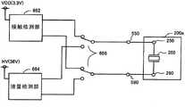
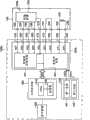
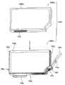
图1是示出本发明一个实施方式中的印刷装置的构成的立体图。印刷装置1000具有安装墨盒的盒安装部1100;转动自如的盖1200;以及操作部1300。该印刷装置1000是在海报等大宽度面纸张(A2~A0大小等)上进行印刷的大型喷墨打印机(Large Format Ink Jet Printer)。将盒安装部1100也称为“盒保持器”,或简称为“保持器”。在图1所示的例子中,在盒安装部1100中可独立地安装四个墨盒,例如安装黑色、黄色、品红色、青色的四种墨盒。作为安装到盒安装部1100的墨盒,也可以采用除此之外的任意多种类型的墨盒。在图1中,为了便于说明,绘出了彼此正交的XYZ轴。+X方向是墨盒100向盒安装部1100插入的方向(以下称为“插入方向”或“安装方向”)。盖1200可打开关闭地安装在盒安装部1100上。盖1200可省去。操作部1300是用于用户进行各种指示或设定的输入装置,并包括用于向用户进行各种通知的显示部。该印刷装置1000具有印刷头;用于进行印刷头的扫描的主扫描运送机构以及副扫描运送机构;以及驱动印刷头来排出墨水的头驱动机构等,但这里省略图示。将如该印刷装置1000这样被用户更换的盒被安装到设置在印刷头的滑架以外的位置的盒安装部中的印刷装置的类型称为“离架型”。FIG. 1 is a perspective view showing the configuration of a printing device according to one embodiment of the present invention. Theprinting apparatus 1000 has acartridge mounting portion 1100 for mounting an ink cartridge; arotatable cover 1200 ; and anoperation portion 1300 . Thisprinting device 1000 is a large format ink jet printer (Large Format Ink Jet Printer) that prints on large-width paper (A2 to A0 size, etc.) such as posters. Thecartridge mounting portion 1100 is also referred to as a "cartridge holder", or simply as a "holder". In the example shown in FIG. 1 , four ink cartridges, for example, black, yellow, magenta, and cyan ink cartridges, can be independently mounted in thecartridge mounting portion 1100 . Any of various types of ink cartridges other than these may be employed as the ink cartridge mounted on thecartridge mounting portion 1100 . In FIG. 1 , for convenience of explanation, XYZ axes orthogonal to each other are drawn. The +X direction is the direction in which theink cartridge 100 is inserted into the cartridge mounting portion 1100 (hereinafter referred to as “insertion direction” or “mounting direction”). Thecover 1200 is attached to thecartridge mounting portion 1100 so as to be openable and closable.Cover 1200 can be omitted. Theoperation unit 1300 is an input device for the user to perform various instructions or settings, and includes a display unit for providing various notifications to the user. Theprinting apparatus 1000 includes a printing head; a main scanning conveyance mechanism and a sub-scanning conveyance mechanism for scanning the printing head; and a head driving mechanism for driving the printing head to discharge ink, etc., although illustration is omitted here. A type of printing apparatus in which a cartridge replaced by a user is mounted in a cartridge mounting portion provided at a position other than the carriage of the print head like thisprinting apparatus 1000 is called an “off-shelf type”.

图2是示出墨盒100的外观的立体图。图2的XYZ轴与图1的XYZ轴对应。将墨盒简称为“盒”。该盒100具有扁平的大致长方体的外观形状,在三个方向的尺寸L1、L2、L3中,长度L1(插入方向的尺寸)最大,宽度L2最小,高度L3是长度L1与宽度L2的中间。但是,根据印刷装置的类型,也存在长度L1小于高度L3的盒。FIG. 2 is a perspective view showing the appearance of theink cartridge 100 . The XYZ axes of FIG. 2 correspond to the XYZ axes of FIG. 1 . The ink cartridge is simply referred to as "cartridge". Thecase 100 has a flat substantially rectangular parallelepiped shape. Among the dimensions L1, L2, and L3 in three directions, the length L1 (dimension in the insertion direction) is the largest, the width L2 is the smallest, and the height L3 is midway between the length L1 and the width L2. However, depending on the type of printing unit, there are also cartridges whose length L1 is smaller than the height L3.

盒100包括:前端面(第一面)Sf、后端面(第二面)Sr、顶面(第三面)St、底面(第四面)Sb、以及两个侧面(第五以及第六面)Sc、Sd。前端面Sf是位于插入方向X的前端的面。前端面Sf和后端面Sr在六个面中最小,并且彼此相对。前端面Sf和后端面Sr均与顶面St、底面Sb以及两个侧面Sc、Sd相交。在盒100安装在盒安装部1100中的状态下,顶面St位于竖直方向的上端,底面Sb位于竖直方向的下端。两个侧面Sc、Sd是六个面中最大的面,并彼此相对。在盒100的内部设置有挠性材料形成的墨水容纳室120(称为“墨水容纳袋”)。墨水容纳室120由于由挠性材料形成,因此随着墨水被消耗而逐渐收缩,并且主要是厚度(Y方向的宽度)逐渐变小。Thebox 100 includes: a front face (first face) Sf, a rear end face (second face) Sr, a top face (third face) St, a bottom face (fourth face) Sb, and two side faces (fifth and sixth faces). ) Sc, Sd. The front end surface Sf is a surface located at the front end in the insertion direction X. As shown in FIG. The front end surface Sf and the rear end surface Sr are the smallest among the six surfaces, and are opposed to each other. Both the front end surface Sf and the rear end surface Sr intersect the top surface St, the bottom surface Sb, and the two side surfaces Sc, Sd. In a state where thecartridge 100 is installed in thecartridge mounting portion 1100 , the top surface St is located at the upper end in the vertical direction, and the bottom surface Sb is located at the lower end in the vertical direction. The two sides Sc, Sd are the largest of the six faces and face each other. Inside thecartridge 100, an ink containing chamber 120 (referred to as an "ink containing bag") formed of a flexible material is provided. Since theink containing chamber 120 is formed of a flexible material, it gradually shrinks as the ink is consumed, and mainly the thickness (width in the Y direction) gradually becomes smaller.

前端面Sf具有两个定位孔131、132以及墨水供应口110。两个定位孔131、132用于定位盒安装部1100内的盒的容纳位置。墨水供应口110与盒安装部1100的墨水供应管连接,从而将盒100内的墨水供应给印刷装置1000。在顶面St上设置有电路基板200。在图2的例子中,电路基板200设置在顶面St的前端(插入方向X最里侧的端部)。但是,电路基板200也可以设置在顶面St的前端附近的其他位置,此外也可以设置在顶面St以外的位置。在电路基板200上安装有用于保存有关墨水的信息的非易失性的存储元件。将电路基板200简称为“基板”。底面Sb具有用于将盒100固定到容纳位置的固定槽140。第一侧面Sc和第二侧面Sd彼此相对,并且与前端面Sf、顶面St、后端面Sr以及底面Sb正交。在第二侧面Sd与前端面Sf相交的位置配置有凹凸嵌合部134。该凹凸嵌合部134与盒安装部1100的凹凸嵌合部一起用于防止盒的误安装。The front surface Sf has twopositioning holes 131 , 132 and anink supply port 110 . The twopositioning holes 131 , 132 are used for positioning the storage position of the cartridge in thecartridge installation part 1100 . Theink supply port 110 is connected to an ink supply tube of thecartridge mounting portion 1100 to supply the ink in thecartridge 100 to theprinting device 1000 . Thecircuit board 200 is provided on the top surface St. In the example of FIG. 2 , thecircuit board 200 is provided at the front end (the innermost end in the insertion direction X) of the top surface St. As shown in FIG. However, thecircuit board 200 may be provided at another position near the front end of the top surface St, or may be provided at a position other than the top surface St. On thecircuit board 200 is mounted a nonvolatile memory element for storing ink-related information. Thecircuit board 200 is simply referred to as a "substrate". The bottom surface Sb has fixinggrooves 140 for fixing thecartridge 100 to the storage position. The first side Sc and the second side Sd are opposed to each other, and are perpendicular to the front surface Sf, the top surface St, the rear surface Sr, and the bottom surface Sb. A concave-convexfitting portion 134 is arranged at a position where the second side surface Sd intersects the front end surface Sf. This concave-convexfitting part 134 is used together with the concave-convex fitting part of thecartridge mounting part 1100 to prevent incorrect installation of the cartridge.

该盒100是大型喷墨打印机用的盒,与用于面向个人的小型喷墨打印机的盒相比,盒尺寸大,并且其中容纳的墨水量也多。例如,相对于在大型喷墨打印机用的盒中盒的长度L1为100mm以上,在小型喷墨打印机用的盒,盒的长度L1为70mm以下。此外,相对于在大型喷墨打印机用的盒中未使用时的墨水量为17ml以上(典型的为100ml以上),在小型喷墨打印机用的盒中,未使用时的墨水量为15ml以下。此外,很多情况下,相对于大型喷墨打印机用的盒在前端面(插入方向的前头的面)与盒安装部机械地连结,小型喷墨打印机用的盒在底面与盒安装部机械地连结。在大型喷墨打印机用的盒中,由于与这样的尺寸、重量、或与盒安装部的连结位置相关的特点,与小型喷墨打印机用的盒相比,具有电路基板200的端子发生接触不良的倾向。关于这一点,在后面进行说明。Thecartridge 100 is a cartridge for a large-sized inkjet printer, and is larger in size than a cartridge for a small-sized inkjet printer for personal use, and holds a larger amount of ink therein. For example, while the length L1 of the cartridge for a large inkjet printer is 100 mm or more, the length L1 of the cartridge for a small inkjet printer is 70 mm or less. In addition, while the unused ink volume is 17ml or more (typically 100ml or more) in the large inkjet printer cartridge, the unused ink volume in the small inkjet printer cartridge is 15ml or less. In addition, in many cases, the cartridge for a large inkjet printer is mechanically connected to the cartridge mounting portion on the front end surface (the front surface in the insertion direction), and the cartridge for a small inkjet printer is mechanically connected to the cartridge mounting portion on the bottom surface. . In a cartridge for a large inkjet printer, due to the characteristics related to such size, weight, or connection position with the cartridge mounting portion, compared with a cartridge for a small inkjet printer, a terminal having acircuit board 200 has poor contact. Propensity. This point will be described later.

然而,以往,一般使用设置在盒上的多个端子中的一个或两个端子进行安装状态的检测。但是,即使在检测到盒被正确安装的情况下,在安装检测中没有使用的其他端子也存在与印刷装置的端子之间的接触不充分的情况。特别是,在存储装置用的端子的接触不充分的情况下,会产生从存储装置读取数据时或者向存储装置写入数据时产生错误的问题。However, conventionally, detection of the mounting state has generally been performed using one or two terminals among a plurality of terminals provided on the box. However, even when it is detected that the cartridge is correctly mounted, other terminals not used for mounting detection may not be in sufficient contact with the terminals of the printing device. In particular, when the contacts of the terminals for the storage device are not sufficient, there is a problem that an error occurs when data is read from the storage device or when data is written to the storage device.

这样的端子接触不良的问题在向海报等大宽度面纸张(A2~A0大小等)进行印刷的大型喷墨打印机用的墨盒中尤其重要。即,在大型喷墨打印机中,墨盒的尺寸大于小型喷墨打印机用的墨盒,并且盒中容纳的墨水重量也多。发明人从这样的尺寸以及重量的差异,发现了大型喷墨打印机与小型喷墨打印机相比具有墨盒易倾斜的倾向。此外,在大型喷墨打印机中,墨盒与盒保持器(也称为“盒安装部”)的连结位置大多设置在墨盒的侧面,另一方面,在小型喷墨打印机中,连结位置大多设置在墨盒的底面。从这种连结位置的差异,也明确了大型喷墨打印机与小型喷墨打印机相比具有墨盒易倾斜的倾斜。如此,在大型喷墨打印机中,由于各种构成原因,与小型喷墨打印机相比,墨盒易倾斜,其结果是,基板的端子具有易发生接触不良的倾向。因此,发明人尤其关于大型喷墨打印机产生了想更可靠地检测存储装置用的端子的接触状态良好的愿望。Such a problem of poor terminal contact is particularly important in ink cartridges for large-sized inkjet printers that print on large-width paper (A2 to A0 sizes, etc.) such as posters. That is, in a large inkjet printer, the size of the ink cartridge is larger than that for a small inkjet printer, and the weight of ink accommodated in the cartridge is also large. From such a difference in size and weight, the inventors have found that the ink cartridges tend to tilt more easily in large inkjet printers than in small inkjet printers. In addition, in large inkjet printers, the connection position between the ink cartridge and the cartridge holder (also called "cartridge mounting part") is often provided on the side of the ink cartridge. On the other hand, in small inkjet printers, the connection position is often provided on the the underside of the cartridge. From this difference in connection position, it is also clear that the large inkjet printer has an inclination that the ink cartridge tends to incline compared to the small inkjet printer. As described above, in a large inkjet printer, due to various structural reasons, the ink cartridge tends to be tilted more easily than in a small inkjet printer, and as a result, poor contact tends to easily occur at the terminals of the substrate. Therefore, the inventors wished to more reliably detect that the contact state of the terminal for a memory device is good, particularly with regard to a large-sized inkjet printer.

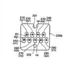
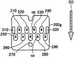
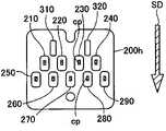
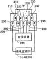
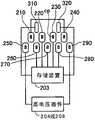
图3A示出了基板200的表面构成。基板200的表面是盒100上安装有基板200时暴露在外侧的面。图3B示出了从侧面观看基板200的图。在基板200的上端部形成有凸台槽201,在基板200的下端部形成有凸台孔202。FIG. 3A shows the surface configuration of thesubstrate 200 . The surface of thesubstrate 200 is a surface exposed to the outside when thesubstrate 200 is mounted on thecartridge 100 . FIG. 3B shows a view of thesubstrate 200 viewed from the side. Aboss groove 201 is formed at the upper end of thesubstrate 200 , and aboss hole 202 is formed at the lower end of thesubstrate 200 .

图3A中的箭头SD示出了向盒安装部1100的盒100的安装方向。该安装方向SD与图2所示的盒的安装方向(X方向)一致。基板200在背面具有存储装置203,在表面设置有包括九个端子210~290的端子群。这些端子210~290从基板200的表面起的高度相同,并且二维地排列在基板200上。存储装置203保存与盒100的墨水相关的信息(例如墨水余量)。端子210~290被形成为大致矩形形状,并被配置成使得与安装方向SD大致垂直的行形成2行。两行中,将安装方向SD的面前侧的行(图3A中位于上侧的行)称为上侧行R1(第一行),将安装方向SD的里侧的行(图3A中位于下侧的行)称为下侧行R2(第二行)。这些行R1、R2也可认为是有多个端子的接触部cp形成的行。印刷装置侧的端子群(后述)在这些接触部cp与基板200上的端子210~290接触。接触部cp充分小于每个端子的面积,并具有大致点状的形状。当盒100被安装到印刷装置时,印刷装置侧的端子群的接触部在基板200上从图3A的下端向上方滑动前进,并在安装完毕时,在与盒侧每个端子对应的印刷装置侧的所有端子的每一个所接触的位置处停止。Arrow SD in FIG. 3A shows the mounting direction of thecartridge 100 to thecartridge mounting portion 1100 . This mounting direction SD corresponds to the mounting direction (X direction) of the cartridge shown in FIG. 2 . Thesubstrate 200 has amemory device 203 on the back surface, and a terminal group including nineterminals 210 to 290 is provided on the front surface. Theseterminals 210 to 290 have the same height from the surface of thesubstrate 200 and are arranged two-dimensionally on thesubstrate 200 . Thestorage device 203 stores information related to the ink of the cartridge 100 (for example, the remaining amount of ink). Theterminals 210 to 290 are formed in a substantially rectangular shape, and are arranged such that rows substantially perpendicular to the mounting direction SD form two rows. Among the two rows, the row on the front side of the installation direction SD (the row on the upper side in FIG. The row on the side) is called the lower row R2 (second row). These rows R1 and R2 can also be regarded as rows formed by contact portions cp having a plurality of terminals. A terminal group (described later) on the printing device side contacts theterminals 210 to 290 on thesubstrate 200 at these contact portions cp. The contact portion cp is sufficiently smaller than the area of each terminal, and has a substantially point-like shape. When thebox 100 is installed on the printing device, the contact portion of the terminal group on the printing device side slides upward from the lower end of FIG. Stop at each position where all terminals on the side are in contact.

形成上侧行R1的端子210~240与形成下侧行R2的端子250~290分别具有以下的功能(用途)。Theterminals 210 to 240 forming the upper row R1 and theterminals 250 to 290 forming the lower row R2 have the following functions (uses), respectively.

上侧行R1:Upper row R1:

(1)安装检测端子210(1) Installdetection terminal 210

(2)复位端子220(2)Reset terminal 220

(3)时钟端子230(3)Clock terminal 230

(4)安装检测端子240(4) Installdetection terminal 240

下侧行R2:Lower side row R2:

(5)安装检测端子250(5) Installdetection terminal 250

(6)电源端子260(6)Power terminal 260

(7)接地端子270(7)Ground terminal 270

(8)数据端子280(8)Data terminal 280

(9)安装检测端子290(9) Installdetection terminal 290

四个安装检测端子210、240、250、290被用于检测与对应的装置侧端子之间的电接触好否,也可以称为“接触检测端子”。此外,也可将安装检测处理称为“接触检测处理”。其他五个端子220、230、260、270、280是存储装置203用的端子,还称为“存储器端子”。The fourinstallation detection terminals 210 , 240 , 250 , and 290 are used to detect whether the electrical contact with the corresponding device-side terminals is good or not, and may also be referred to as “contact detection terminals”. In addition, the mounting detection processing may also be called "contact detection processing". The other fiveterminals 220, 230, 260, 270, and 280 are terminals for thestorage device 203, and are also referred to as "memory terminals".

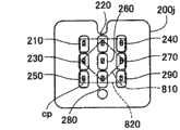
多个端子210~290的每一个分别在其中央部包含与多个装置侧端子中的对应的端子接触的接触部cp。形成上侧行R1的端子210~240的各接触部cp与形成下侧行R2的端子250~290的各接触部cp彼此不同地配置,构成了所谓锯齿形的配置。此外,形成上侧行R1的端子210~240与形成下侧行R2的端子250~290也彼此不同地配置以使彼此的端子中心不在安装方向SD上排列,构成了锯齿形的配置。Each of the plurality ofterminals 210 to 290 includes a contact portion cp in its central portion that contacts a corresponding terminal among the plurality of device-side terminals. The respective contact portions cp of theterminals 210 to 240 forming the upper row R1 and the respective contact portions cp of theterminals 250 to 290 forming the lower row R2 are arranged differently from each other, forming a so-called zigzag arrangement. In addition, the terminals 210 - 240 forming the upper row R1 and the terminals 250 - 290 forming the lower row R2 are also arranged differently from each other so that the centers of the terminals are not aligned in the mounting direction SD, forming a zigzag arrangement.

上侧行R1的两个安装检测端子210、240的各个接触部分别配置在上侧行R1的两端部,即上侧行R1的最外侧。此外,下侧行R2的两个安装检测端子250、290的各个接触部分别配置在下侧行R2的两端部,即下侧行R2的最外侧。存储器端子220、230、260、270、280的接触部集中配置在多个端子210~290全体被配置的区域内的大致中央。此外,四个安装检测端子210、240、250、290的接触部配置在存储器端子220、230、260、270、280的集合的四个角上。The respective contact portions of the two mountingdetection terminals 210 and 240 in the upper row R1 are arranged at both ends of the upper row R1 , that is, at the outermost sides of the upper row R1 . In addition, the respective contact portions of the two mountingdetection terminals 250 and 290 in the lower row R2 are arranged at both ends of the lower row R2 , that is, at the outermost sides of the lower row R2 . The contacts of thememory terminals 220 , 230 , 260 , 270 , and 280 are collectively arranged substantially at the center of the region where all theterminals 210 to 290 are arranged. In addition, the contact portions of the four mountingdetection terminals 210 , 240 , 250 , and 290 are arranged at the four corners of the set ofmemory terminals 220 , 230 , 260 , 270 , and 280 .

图3C示出了图3A所示的九个端子210~290的接触部210cp~290cp。九个接触部210cp~290cp以基本固定的间隔大致均匀地配置。存储装置用的多个接触部220cp、230cp、260cp、270cp、280cp配置在接触部210cp~290cp全体被配置的区域内的中央区域(第一区域810)中。四个安装检测端子的接触部210cp、240cp、250cp、290cp被配置在第一区域810的外侧。此外,四个安装检测端子的接触部210cp、240cp、250cp、290cp配置在包含第一区域810的四边形的第二区域820的四个角上。第一区域810的形状优选为包含四个安装检测端子的接触部210cp、240cp、250cp、290cp的面积最小的四边形。或者,也可以将第一区域810的形状设为与四个安装检测端子的接触部210cp、240cp、250cp、290cp外切的四边形。第二区域820的形状优选为包含全部接触部210cp~290cp的面积最小的四边形。此外,当沿图2B的竖直向下(-Z方向)观看时,包含存储装置用的多个接触部220cp、230cp、260cp、270cp、280cp的第一区域810的中心优选被配置成处于盒100的墨水供应口110(图2)的中心线上。FIG. 3C shows contact portions 210cp-290cp of the nine terminals 210-290 shown in FIG. 3A. The nine contact portions 210cp to 290cp are substantially evenly arranged at substantially constant intervals. The plurality of contacts 220cp, 230cp, 260cp, 270cp, and 280cp for a memory device are arranged in a central region (first region 810 ) within the region where all the contacts 210cp to 290cp are arranged. The contact portions 210cp, 240cp, 250cp, and 290cp of the four mounting detection terminals are arranged outside thefirst region 810 . In addition, the contact portions 210cp, 240cp, 250cp, and 290cp of the four mounting detection terminals are arranged at the four corners of the quadrangularsecond region 820 including thefirst region 810 . The shape of thefirst region 810 is preferably a quadrangle with the smallest area including the contact portions 210cp, 240cp, 250cp, and 290cp of the four mounting detection terminals. Alternatively, the shape of thefirst region 810 may be a quadrangle circumscribing the contact portions 210cp, 240cp, 250cp, and 290cp of the four mounting detection terminals. The shape of thesecond region 820 is preferably a quadrangle with the smallest area including all the contact portions 210cp to 290cp. In addition, when viewed vertically downward (-Z direction) in FIG. 2B , the center of thefirst region 810 containing the plurality of contacts 220cp, 230cp, 260cp, 270cp, 280cp for the storage device is preferably configured to be in thebox 100 on the center line of the ink supply port 110 (FIG. 2).

在本实施方式中,第二区域820为梯形。第二区域820的形状优选为上底(第一底边)小于下底(第二底边)的等腰梯形。在印刷装置中盒100完成安装的状态下,四个安装检测端子210、240、250、290的接触部210cp、240cp、250cp、290cp优选被配置在梯形形状的第二区域820的上底的两端附近和下底的两端附近(即,图3A中的上侧行R1的两端和下侧行R2的两端)。该理由如下所述。在盒100安装在印刷装置中的状态下,盒100的墨水供应口110(参见图2B)与印刷装置的墨水供应管(后述)连接。从而,如果盒100以墨水供应口110为中心从正确的安装位置向±Y方向倾斜,则离墨水供应口110最远的端子以最大的偏离量从端子中央偏离的可能性高。在本实施方式中,在位于上侧行R1的端子210~240中,离墨水供应口110最远的端子是位于上侧行R1的两端的安装检测端子210、240。此外,在位于下侧行R2的端子250~290中,离墨水供应口110最远的端子是位于下侧行R2的两端的安装检测端子250、290。另一方面,假使将两行的端子群排成矩形形状(矩阵状)而不是排成锯齿状,则包含基板200上的接触部cp的第二区域820也为矩形。在此情况下,存在于上侧行R1上的安装检测端子210、240与存在于下侧行R2上的安装检测端子250、290相比位于离墨水供应口110更远的位置,因此从对应的装置侧端子偏离更多。此时,即使假定其他端子220、230、250~290处于正确的接触状态,位于上侧行R1的安装检测端子210、240的接触状态也有可能不充分,从而可能被判定为安装不良。从而,为了降低这种误判定的可能性,四个安装检测端子210、240、250、290的接触部210cp、240cp、250cp、290cp优选配置在梯形形状的第二区域820的上底的两端和下底的两端。将包含基板200上的全部接触部的第二区域820设为梯形形状的优点在后述的其他实施方式中也基本相同。In this embodiment, thesecond region 820 is trapezoidal. The shape of thesecond region 820 is preferably an isosceles trapezoid whose upper base (first base) is smaller than the lower base (second base). In the state where thecartridge 100 is installed in the printing device, the contact portions 210cp, 240cp, 250cp, and 290cp of the fourinstallation detection terminals 210, 240, 250, and 290 are preferably arranged on two sides of the upper bottom of the trapezoidal-shapedsecond region 820. Near the end and near both ends of the lower bottom (ie, both ends of the upper row R1 and both ends of the lower row R2 in FIG. 3A ). The reason for this is as follows. In a state where thecartridge 100 is installed in the printing apparatus, the ink supply port 110 (see FIG. 2B ) of thecartridge 100 is connected to an ink supply tube (described later) of the printing apparatus. Therefore, if thecartridge 100 is tilted in the ±Y direction from the correct mounting position centering on theink supply port 110 , the terminal farthest from theink supply port 110 is likely to deviate from the center of the terminal by the largest amount of deviation. In this embodiment, among theterminals 210 to 240 located in the upper row R1 , the terminal farthest from theink supply port 110 is the mountingdetection terminals 210 and 240 located at both ends of the upper row R1 . In addition, among theterminals 250 to 290 located in the lower row R2 , the terminal farthest from theink supply port 110 is the mountingdetection terminals 250 and 290 located at both ends of the lower row R2 . On the other hand, if the terminal groups of two rows are arranged in a rectangular shape (matrix) instead of zigzag, thesecond region 820 including the contact portion cp on thesubstrate 200 is also rectangular. In this case, the mountingdetection terminals 210, 240 present on the upper row R1 are located farther from theink supply port 110 than the mountingdetection terminals 250, 290 present on the lower row R2, and thus are located farther from theink supply port 110. The device side terminals of the device deviate more. At this time, even if theother terminals 220, 230, 250 to 290 are assumed to be in the correct contact state, the contact state of the mountingdetection terminals 210, 240 located in the upper row R1 may be insufficient, and may be determined as a mounting failure. Thereby, in order to reduce the possibility of this misjudgment, the contact portions 210cp, 240cp, 250cp, 290cp of the fourinstallation detection terminals 210, 240, 250, 290 are preferably arranged at both ends of the upper bottom of the trapezoidalsecond region 820 and the ends of the lower bottom. The advantage of making thesecond region 820 including all the contact portions on thesubstrate 200 trapezoidal is basically the same in other embodiments described later.

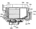
图4A~图4C是盒安装部1100的构成的图。图4A是从斜后方观看盒安装部1100的立体图,图4B是从盒安装部1100的正面(插入盒的口)观看盒安装部1100的内部的图。图4C是将盒安装部1100的内部截面观看的图。在图4A~图4C中,为了便于图示,省略了一部分壁部件等。图4A~图4C的XYZ轴相当于图1、图2的XYZ轴。盒安装部1100包括用于容纳盒的四个容纳槽SL1~SL4。如图4B所示,在盒安装部1100内的每个狭槽中,设置有墨水供应管1180、一对定位销1110、1120、凹凸嵌合部1140、以及触点机构1400。如图4C所示,墨水供应管1180、一对定位销1110、1120、凹凸嵌合部1140被固定在盒安装部的里侧壁部件1160上。墨水供应管1180、定位销1110、1120、以及凹凸嵌合部1140被插入到设置在滑板部件1150上的通孔1181、1111、1121、1141中,并朝向与盒的安装方向相反的方向突出配置。图4A是取下里侧壁部件1160并从背面侧观看滑板部件1150的图。在图4A中,省略定位销进行了图示。如图4A所示,在滑板部件1150的背面侧设置有与一对定位销1110、1120对应的一对施力弹簧1112、1122。如图4C所示,一对施力弹簧1112、1122以固定在滑板部件1150和里侧壁部件1160上的方式配置。4A to 4C are diagrams showing the configuration of thecartridge mounting unit 1100 . 4A is a perspective view of thecartridge mounting unit 1100 viewed obliquely from behind, and FIG. 4B is a view of the inside of thecartridge mounting unit 1100 viewed from the front side of the cartridge mounting unit 1100 (the opening where the cartridge is inserted). FIG. 4C is a diagram of an internal section of thecartridge mounting unit 1100 viewed. In FIGS. 4A to 4C , for convenience of illustration, some wall members and the like are omitted. The XYZ axes in FIGS. 4A to 4C correspond to the XYZ axes in FIGS. 1 and 2 . Thecartridge installation part 1100 includes four accommodation slots SL1 to SL4 for accommodating a cartridge. As shown in FIG. 4B , in each slot in thecartridge mounting portion 1100 , anink supply tube 1180 , a pair ofpositioning pins 1110 , 1120 , a concave-convexfitting portion 1140 , and acontact mechanism 1400 are provided. As shown in FIG. 4C , theink supply tube 1180 , a pair ofpositioning pins 1110 , 1120 , and the concave-convexfitting portion 1140 are fixed to the innerside wall member 1160 of the cartridge mounting portion. Theink supply tube 1180, the positioning pins 1110, 1120, and the concave-convexfitting part 1140 are inserted into the throughholes 1181, 1111, 1121, 1141 provided on theslider member 1150, and protrude in a direction opposite to the cartridge mounting direction. . FIG. 4A is a view of theslide member 1150 viewed from the rear side with the innerside wall member 1160 removed. In FIG. 4A , the positioning pins are omitted from illustration. As shown in FIG. 4A , a pair of urgingsprings 1112 and 1122 corresponding to the pair ofpositioning pins 1110 and 1120 are provided on the back side of theslider member 1150 . As shown in FIG. 4C , a pair of urgingsprings 1112 and 1122 are arranged so as to be fixed to theslider member 1150 and theback wall member 1160 .

墨水供应管1180被插入盒100的墨水供应110(图2A)中,并用于向印刷装置1000内部的印刷头供应墨水。当向盒安装部1100插入盒100时,定位销1110、1120被插入到设置在盒100上的定位孔131、132中,以用于固定盒100的容纳位置。凹凸嵌合部1140具有与盒100的凹凸嵌合部134的形状对应的形状,并针对每个容纳槽SL1~SL4,具有不同的形状。由此,每个容纳槽SL1~SL4中只可容纳其中容纳预先确定的一种墨水的盒,而无法容纳其他颜色的盒。Theink supply tube 1180 is inserted into the ink supply 110 ( FIG. 2A ) of thecartridge 100 and is used to supply ink to the printheads inside theprinting device 1000 . When thecartridge 100 is inserted into thecartridge mounting portion 1100 , the positioning pins 1110 , 1120 are inserted into the positioning holes 131 , 132 provided on thecartridge 100 to fix the receiving position of thecartridge 100 . The concave-convexfitting portion 1140 has a shape corresponding to the shape of the concave-convexfitting portion 134 of thecartridge 100 , and has a different shape for each of the storage grooves SL1 to SL4 . Therefore, each of the storage slots SL1 to SL4 can only accommodate a cartridge of a predetermined type of ink therein, and cannot accommodate cartridges of other colors.

配置在每个容纳槽的里侧壁面上的滑板部件1150被构成为可向盒的安装方向(X方向)以及排出方向(-X方向)滑动。设置在每个容纳槽中的一对施力弹簧1112、1122(图4A)将滑板部件1150向排出方向施力。当盒100被插入容纳槽中时,该盒100向安装方向推压滑板部件1150和一对施力弹簧1112、1122,从而反抗施力弹簧1112、1122的施力推进。从而,在盒100容纳在盒安装部1100中的状态下,一对施力弹簧1112、1122将盒100向排出方向施力。此外,在该容纳状态下,设置在每个容纳槽SL1~SL4的底部的固定部件1130(图4B)与设置盒100的底面Sb的固定槽140(图2A)配合。通过该固定部件1130与固定槽140的配合,防止了盒100通过施力弹簧1112、1122的施力而从盒安装部1100被排出。Theslider member 1150 disposed on the back wall surface of each storage groove is configured to be slidable in the cartridge mounting direction (X direction) and ejection direction (−X direction). A pair of urgingsprings 1112, 1122 (FIG. 4A) disposed in each receiving groove urges theslide member 1150 in the discharge direction. When thecartridge 100 is inserted into the accommodating groove, thecartridge 100 pushes theslide member 1150 and the pair of urgingsprings 1112 , 1122 in the mounting direction, thereby pushing against the urging force of the urging springs 1112 , 1122 . Therefore, when thecartridge 100 is accommodated in thecartridge mounting portion 1100 , the pair of urgingsprings 1112 and 1122 urge thecartridge 100 in the discharge direction. Also, in this accommodated state, the fixing member 1130 ( FIG. 4B ) provided at the bottom of each of the housing grooves SL1 ˜ SL4 engages with the fixing groove 140 ( FIG. 2A ) provided on the bottom surface Sb of thecartridge 100 . The cooperation between the fixingmember 1130 and the fixinggroove 140 prevents thecartridge 100 from being ejected from thecartridge installation part 1100 by the urging force of the urgingsprings 1112 and 1122 .

在排出盒100的情况下,当用户先向安装方向推入了盒100时,随之固定部件1130与固定槽140之间的配合被解除。其结果是,盒100通过一对施力弹簧1112、1122的施力而向排出方向(-X方向)被推出。从而,用户能够从盒安装部1100容易地取出盒100。When thecartridge 100 is ejected, when the user first pushes thecartridge 100 in the installation direction, the engagement between the fixingmember 1130 and the fixinggroove 140 is released accordingly. As a result, thecartridge 100 is pushed out in the discharge direction (−X direction) by the urging force of the pair of urgingsprings 1112 and 1122 . Thus, the user can easily take out thecartridge 100 from thecartridge mounting portion 1100 .

触点机构1400(图4B)具有多个装置侧端子,当盒100被插入到盒安装部1100中时,所述多个装置侧端子与电路基板200的端子210~290(图3A)接触并导通。印刷装置1000的控制电路经由该触点机构1400を在与电路基板200之间进行信号的收发。The contact mechanism 1400 ( FIG. 4B ) has a plurality of device-side terminals that come into contact with theterminals 210 to 290 ( FIG. 3A ) of thecircuit board 200 when thecartridge 100 is inserted into thecartridge mounting portion 1100 . conduction. The control circuit of theprinting apparatus 1000 transmits and receives signals to and from thecircuit board 200 via thecontact mechanism 1400 .

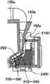
图5A示出了盒100被恰当地安装在盒安装部1100内的状态。在该状态下,盒100没有发生倾斜,其上面和底面处于与盒安装部1100的上端部件和下端部件平行的状态。盒安装部1100的墨水供应管1180与盒100的墨水供应口110连结,盒安装部1100的定位销1110、1120被插入盒100的定位孔131、132中。并且,设置在盒安装部1100的底部的固定部件1130与设置在盒100的底面的固定槽140配合。而且,盒安装部1100的一对施力弹簧1112、1122将盒的前端面Sf向排出方向施力。在盒100被恰当地安装的状态下,盒安装部1100的触点机构1400与盒100的基板200的端子210~290(图3A)彼此以良好的接触状态接触。FIG. 5A shows a state where thecartridge 100 is properly installed in thecartridge mounting portion 1100 . In this state, thecartridge 100 is not tilted, and its upper and lower surfaces are parallel to the upper end member and the lower end member of thecartridge mounting portion 1100 . Theink supply tube 1180 of thecartridge mount 1100 is connected to theink supply port 110 of thecartridge 100 , and the positioning pins 1110 , 1120 of thecartridge mount 1100 are inserted into the positioning holes 131 , 132 of thecartridge 100 . And, the fixingpart 1130 provided at the bottom of thecartridge installation part 1100 is engaged with the fixinggroove 140 provided at the bottom surface of thecartridge 100 . Furthermore, a pair of urgingsprings 1112 and 1122 of thecartridge mounting portion 1100 urges the front end surface Sf of the cartridge in the discharge direction. When thecartridge 100 is properly mounted, thecontact mechanism 1400 of thecartridge mounting portion 1100 and theterminals 210 to 290 ( FIG. 3A ) of thesubstrate 200 of thecartridge 100 are in good contact with each other.

然而,盒安装部1100的内部多少有些游隙,以便容易安装盒100。因此,盒100不限于以图5A所示那样没有倾斜而直立着的恰当的状态被收纳,有时会以与盒的宽度方向(Y方向)平行的轴为中心发生倾斜。具体地,会产生如图5B所示那样以盒的后端稍稍下降的状态倾斜的情况,或者相反地,会产生如图5C所示那样以盒的后端稍稍上升的状态倾斜的情况。特别是,当随着墨水被消耗而墨水界面LL逐渐下降时,随着所容纳的墨水重量的改变,重心会发生变化,或者施力弹簧1112、1122的施力与包括墨水重量在内的盒重量之间的平衡会改变。并且,随着该重量平衡的变化,盒具有容易倾斜的倾向。一旦盒发生倾斜,设置在盒的基板200上的多个端子中的一些端子有可能发生接触不良。特别是,在图5B、图5C的状态下,基板200(图3A)的上侧行R1的端子群210~240和下侧行R2的端子群250~290中的一者的一个以上的端子有可能发生接触不良。However, the inside of thecartridge mounting portion 1100 has some play so that thecartridge 100 can be easily mounted. Therefore, thecartridge 100 is not limited to being stored in an appropriate upright state without inclination as shown in FIG. 5A , and may be inclined about an axis parallel to the width direction (Y direction) of the cartridge. Specifically, the case may be inclined with the rear end of the case slightly lowered as shown in FIG. 5B , or conversely, the case may be inclined with the rear end of the case slightly raised as shown in FIG. 5C . In particular, when the ink interface LL is gradually lowered as the ink is consumed, the center of gravity changes as the weight of the contained ink changes, or the biasing force of the biasing springs 1112, 1122 varies with the weight of the cartridge including the weight of the ink. The balance between the weights will change. In addition, the case tends to tilt easily as the weight balance changes. Once the cartridge is tilted, some of the terminals provided on thesubstrate 200 of the cartridge may suffer from poor contact. In particular, in the state of FIG. 5B and FIG. 5C, one or more terminals of one of the terminal groups 210-240 of the upper row R1 and the terminal groups 250-290 of the lower row R2 of the substrate 200 (FIG. 3A) Poor contact may occur.

此外,当盒发生倾斜时,有时还会同时发生与图5B、图5C垂直的反向的倾斜(以与安装方向X平行的轴为中心的倾斜)。此时,图3A所示的基板200也以与其安装方向SD平行的轴为中心向左右倾斜,基板200的处于左侧的端子群210、220、250、260和处于右侧的端子群230、240、280、290中的一者的一个以上的端子有可能发生接触不良。In addition, when the cartridge is tilted, a tilt opposite to that perpendicular to FIGS. 5B and 5C (tilt centered on an axis parallel to the mounting direction X) may also occur simultaneously. At this time, thesubstrate 200 shown in FIG. 3A is also inclined to the left and right with the axis parallel to its mounting direction SD as the center, and theterminal groups 210, 220, 250, 260 on the left side of thesubstrate 200 and theterminal groups 230, 260 on the right side of thesubstrate 200 One or more terminals of one of 240, 280, and 290 may have poor contact.

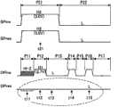
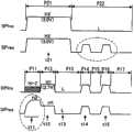
一旦发生这样的接触不良,就会产生盒的存储装置203与印刷装置1000之间的信号收发不能正常地进行的问题。此外,如果墨滴或尘埃等异物附着到基板200的端子附近,有时会在端子之间发生不希望的的短路或漏电。下面说明的各种实施方式中的安装状态的检测处理为了检测由这种盒的倾斜引起的接触不良或者检测由异物引起的不希望的的短路或漏电而执行。If such poor contact occurs, there will be a problem that the signal transmission and reception between thecartridge storage device 203 and theprinting device 1000 cannot be performed normally. In addition, if foreign matter such as ink droplets or dust adheres to the vicinity of the terminals of thesubstrate 200, an undesired short circuit or electric leakage may sometimes occur between the terminals. The mounting state detection processing in the various embodiments described below is performed to detect poor contact caused by such a tilt of the cartridge, or to detect undesired short circuits or electric leakage caused by foreign objects.

然而,大型喷墨打印机用的盒与面向个人的小型喷墨打印机用的盒相比,具有如下的特点。However, the cartridges for large inkjet printers have the following features compared to the cartridges for small inkjet printers for personal use.

(1)盒尺寸大(长度L1为100mm以上)。(1) The box size is large (the length L1 is 100 mm or more).

(2)所容纳的墨水量多(为17ml以上,典型的为100ml以上)。(2) The amount of ink contained is large (17 ml or more, typically 100 ml or more).

(3)在前端面(安装方向的前头的面)与盒安装部机械连结。(3) The front end surface (the front surface in the installation direction) is mechanically connected to the cartridge installation part.

(4)墨水容纳室内的空间未被分隔,构成了单一的墨水容纳室(墨水容纳袋)。(4) The space in the ink storage chamber is not divided, and a single ink storage chamber (ink storage bag) is constituted.

根据大型喷墨打印机的类型,也使用不具有这些特点(1)~(4)中的一些特点的盒,但一般具有这些特点中的这少一个特点。Depending on the type of large inkjet printer, cartridges that do not have some of these features (1) to (4) are also used, but generally have this one or less of these features.

大型喷墨打印机用的盒由于具有这种尺寸、重量、与盒安装部的连结位置、或墨水室构成的特点,因此与小型喷墨打印机用的盒相比,盒容易倾斜,其结果是,具有基板200的端子容易发生接触不良的倾向。从而,尤其对于大型喷墨打印机及其盒来说,进行诸如下面说明的那样的端子的接触不良、不希望的的短路、漏电等的检测处理的意义很大。Due to the characteristics of the size, weight, connection position with the cartridge mounting part, or ink chamber configuration of the cartridge for a large inkjet printer, the cartridge tends to tilt compared with a cartridge for a small inkjet printer. As a result, There is a tendency that the terminals of thesubstrate 200 tend to have poor contact. Therefore, especially for large-sized inkjet printers and their cartridges, it is of great significance to perform detection processes such as poor contact of terminals, unintended short circuits, electric leakage, etc. as described below.

图6是示出第一实施方式中的盒的基板200与印刷装置1000的电构成的框图。印刷装置1000包括:显示面板430、电源电路440、主控制电路400、以及副控制电路500。显示面板430是用于向用户进行印刷装置1000的动作状态或盒安装状态等的各种通知的显示部。显示面板430例如设置在图1的操作部1300上。电源电路440具有生成第一电源电压VDD的第一电源441、以及生成第二电源电压VHV的第二电源442。第一电源电压VDD是用于逻辑电路的通常的电源电压(额定3.3V)。第二电源电压VHV是为驱动印刷头来排出墨水而使用的高电压(例如,额定42V)。这些电压VDD、VHV被供应给副控制电路500,并且根据需要还被供应给其他电路。主控制电路400具有CPU 410和存储器420。副控制电路500具有存储器控制电路501和安装检测电路600。也可以将包括主控制电路400和副控制电路500的电路称为“控制电路”。FIG. 6 is a block diagram showing the electrical configuration of thesubstrate 200 of the cartridge and theprinting device 1000 in the first embodiment. Theprinting device 1000 includes: adisplay panel 430 , apower supply circuit 440 , amain control circuit 400 , and asub-control circuit 500 . Thedisplay panel 430 is a display unit for performing various notifications to the user such as the operating state of theprinting apparatus 1000 and the cartridge installation state.Display panel 430 is provided, for example, onoperation unit 1300 in FIG. 1 . Thepower supply circuit 440 has afirst power supply 441 that generates a first power supply voltage VDD, and asecond power supply 442 that generates a second power supply voltage VHV. The first power supply voltage VDD is a common power supply voltage (nominal 3.3V) for logic circuits. The second power supply voltage VHV is a high voltage (for example, nominally 42V) used to drive the print head to discharge ink. These voltages VDD, VHV are supplied to thesub-control circuit 500, and are also supplied to other circuits as necessary. Themain control circuit 400 has aCPU 410 and amemory 420. Thesub control circuit 500 has amemory control circuit 501 and a mountingdetection circuit 600 . A circuit including themain control circuit 400 and thesub-control circuit 500 may also be referred to as a "control circuit".

在设置在盒的基板200(图3A)上的九个端子中,复位端子220、时钟端子230、电源端子260、接地端子270、以及数据端子280与存储装置203电连接。存储装置203是非易失性存储器,该非易失性存储器不具有地址端子,其基于从时钟端子输入的时钟信号SCK的脉冲数和从数据端子输入的指令数据来确定要访问的存储单元,并与时钟信号SCK同步地从数据端子接收数据,或者从数据端子发送数据。时钟端子230用于从副控制电路500向存储装置203提供时钟信号SCK。从印刷装置1000分别向电源端子260和接地端子270提供用于驱动存储装置的电源电压(例如,额定3.3V)和接地电压(0V)。所述用于驱动存储装置203的电源电压是从第一电源电压VDD直接提供的电压,或者是从第一电源电压VDD生成的电压,也可以是比第一电源电压VDD低的电压。数据端子280用于在副控制电路500与存储装置203之间传递数据信号SDA。复位端子220用于从副控制电路500向存储装置203提供复位信号RST。四个安装检测端子210、240、250、290在盒100的基板200(图3A)内经由配线相互连接,并且全部被接地。例如,安装检测端子210、240、250、290通过与接地端子270连接而被接地。但是,也可以通过接地端子270以外的路径来接地。如从上述说明可知的那样,安装检测端子210、240、250、290虽也可以与存储器端子中的一部分(或存储装置203)连接,但优选不连接到接地端子以外的存储器端子和存储装置。特别是,如果安装检测端子与存储器端子和存储装置完全不连接,则安装检查信号以外的信号和电压不被施加到安装检测端子上,从而在可更可靠地进行安装检测的方面上是优选的。在图6的例子中,四个安装检测端子210、240、250、290通过配线连接,但也可以将连接这些端子的配线的一部分替换成电阻。将两个端子通过配线连接的状态也称为“短路连接”或“导线连接”。通过配线的短路连接是与不希望的的短路不同的状态。Among nine terminals provided on the substrate 200 ( FIG. 3A ) of the cartridge, areset terminal 220 , aclock terminal 230 , apower terminal 260 , aground terminal 270 , and adata terminal 280 are electrically connected to thememory device 203 . Thestorage device 203 is a nonvolatile memory which does not have an address terminal, which determines a memory cell to be accessed based on the number of pulses of a clock signal SCK input from a clock terminal and instruction data input from a data terminal, and Data is received from the data terminal in synchronization with the clock signal SCK, or data is transmitted from the data terminal. Theclock terminal 230 is used to supply the clock signal SCK from thesub-control circuit 500 to thestorage device 203 . A power supply voltage (for example, nominally 3.3 V) and a ground voltage (0 V) for driving the storage device are supplied from theprinting device 1000 to thepower supply terminal 260 and theground terminal 270 , respectively. The power supply voltage for driving thestorage device 203 is a voltage directly provided from the first power supply voltage VDD, or a voltage generated from the first power supply voltage VDD, or a voltage lower than the first power supply voltage VDD. Thedata terminal 280 is used to transmit the data signal SDA between thesub-control circuit 500 and thestorage device 203 . Thereset terminal 220 is used to supply a reset signal RST from thesub-control circuit 500 to thestorage device 203 . The four mountingdetection terminals 210 , 240 , 250 , and 290 are connected to each other via wiring in the substrate 200 ( FIG. 3A ) of thecartridge 100 , and all are grounded. For example,attachment detection terminals 210 , 240 , 250 , and 290 are connected to ground terminal 270 to be grounded. However, it is also possible to ground through a path other than theground terminal 270 . As can be seen from the above description, the mountingdetection terminals 210, 240, 250, and 290 may be connected to some memory terminals (or the storage device 203), but are preferably not connected to memory terminals and storage devices other than ground terminals. In particular, if the mounting detection terminal is not connected to the memory terminal and the storage device at all, signals and voltages other than the mounting inspection signal are not applied to the mounting detection terminal, which is preferable in that mounting detection can be performed more reliably. . In the example of FIG. 6 , the four mountingdetection terminals 210 , 240 , 250 , and 290 are connected by wires, but part of the wires connecting these terminals may be replaced with resistors. The state where two terminals are connected by wiring is also called "short circuit connection" or "wire connection". A short-circuited connection through wiring is a different state from an undesired short-circuit.

在图6中,在通过装置侧端子510~590和基板200的端子210~290而连接副控制电路500和基板200的配线路径中标注了配线名SCK、VDD、SDA、RST、OV1、OV2、DT1、DT2。在这些配线名中,存储装置用的配线路径的配线名使用了与信号名相同的名称。装置侧端子510~590被设置在图4B以及图5A所示的触点机构1400中。In FIG. 6, the wiring names SCK, VDD, SDA, RST, OV1, OV2, DT1, DT2. Among these wiring names, the same wiring names as the signal names are used for the wiring paths for the storage device. The device-side terminals 510 to 590 are provided in thecontact mechanism 1400 shown in FIGS. 4B and 5A .

图7示出了基板200与安装检测电路600的连接状态。基板200的四个安装检测端子210、240、250、290经由对应的装置侧端子510、540、550、590与安装检测电路600连接。此外,基板200的四个安装检测端子210、240、250、290被接地。连接装置侧端子510、540、550、590和安装检测电路600的配线分别经由上拉电阻被连接在副控制电路500内的电源VDD(额定3.3V)上。FIG. 7 shows a connection state of thesubstrate 200 and the mountingdetection circuit 600 . The four mountingdetection terminals 210 , 240 , 250 , and 290 of thesubstrate 200 are connected to the mountingdetection circuit 600 via corresponding device-side terminals 510 , 540 , 550 , and 590 . In addition, the four mountingdetection terminals 210, 240, 250, and 290 of thesubstrate 200 are grounded. The wires connecting thedevice side terminals 510 , 540 , 550 , and 590 to the mountingdetection circuit 600 are connected to the power supply VDD (rated at 3.3 V) in thesub-control circuit 500 via pull-up resistors, respectively.

在图7的例子中,基板200的四个安装检测端子210、240、250、290中的三个端子210、240、250处于与对应的装置侧端子510、540、550良好的连接状态。另一方面,第四个安装检测端子290处于与对应的装置侧端子590处于接触不良的状态。连接状态良好的三个装置侧端子510、540、550的配线的电压为L电平(接地电压电平),另一方面,连接状态不良的装置侧端子590的配线的电压为H电平(电源电压VDD电平)。从而,安装检测电路600通过检查这些各配线的电压电平,可对四个安装检测端子210、240、250、290的每个端子判定接触状态的好否。In the example of FIG. 7 , threeterminals 210 , 240 , 250 of the four mountingdetection terminals 210 , 240 , 250 , 290 on thesubstrate 200 are in a good connection state with the corresponding device-side terminals 510 , 540 , 550 . On the other hand, the fourthattachment detection terminal 290 is in a state of poor contact with the corresponding device-side terminal 590 . The voltage of the wiring of the three device-side terminals 510, 540, and 550 in a good connection state is L level (ground voltage level), while the voltage of the wiring of the device-side terminal 590 in a bad connection state is H level. level (power supply voltage VDD level). Therefore, the mountingdetection circuit 600 can determine whether the contact state is good or not for each of the four mountingdetection terminals 210 , 240 , 250 , and 290 by checking the voltage levels of these wirings.

基板200的四个安装检测端子210、240、250、290的各个接触部cp配置在存储装置用的端子220、230、260、270、280的接触部cp的集合区域810的周围的四个角上。当四个安装检测端子210、240、250、290的接触状态都良好时,盒没有发生大的倾斜,存储装置用的端子220、230、260、270、280的接触状态也良好。另一方面,当四个安装检测端子210、240、250、290中一个以上的端子的接触状态不良时,盒发生了大的倾斜,存储装置用的端子220、230、260、270、280中一个以上的端子的接触状态也有可能不良。当四个安装检测端子210、240、250、290中一个以上的接触状态不良时,安装检测电路600优选在显示面板430上显示表示其未安装状态的信息(文字和/或图像)来通知用户。The contact portions cp of the four mountingdetection terminals 210, 240, 250, and 290 of thesubstrate 200 are arranged at the four corners around thecollective area 810 of the contact portions cp of theterminals 220, 230, 260, 270, and 280 for the storage device. superior. When the four mountingdetection terminals 210, 240, 250, 290 are in good contact state, the cartridge is not greatly tilted, and the contact state of thememory device terminals 220, 230, 260, 270, 280 is also good. On the other hand, when the contact state of more than one of the fourinstallation detection terminals 210, 240, 250, 290 is poor, the case is greatly tilted, and theterminals 220, 230, 260, 270, 280 for the storage device The contact state of one or more terminals may be poor. When more than one of the fourinstallation detection terminals 210, 240, 250, 290 has a bad contact state, theinstallation detection circuit 600 preferably displays information (text and/or image) representing its uninstalled state on thedisplay panel 430 to notify the user .

在存储装置用的端子的接触部cp的集合区域810的周围的四个角全部设置安装检测端子的接触部cp的理由如下:在将盒100安装在盒安装部1100中的状态下,盒100也有一定程度倾斜的自由度,因此有时盒100的基板200与盒安装部1100的触点机构1400(图5A)会相互倾斜。例如,当盒100的后端如图5B所示倾斜、从而基板200的上侧行R1的端子群210~240(其接触部群)比下侧行R2的端子群250~290(其接触部群)更远离触点机构1400时,上侧行R1的端子群210~240有可能接触不良。相反地,当盒100的后端如图5C所示倾斜、从而基板200的下侧行R2的端子群250~290比上侧行R1的端子群210~240更远离触点机构1400时,基板200的下侧行R2的五个端子250~290有可能接触不良。此外,当盒100与图5B、图5C不同地以与X方向平行的轴为中心发生了倾斜、从而图7中的基板200的左端比右端更远离触点机构1400时,基板200的位于左侧的端子210、220、250、260、270有可能接触不良。相反地,当基板200的右端比左端更远离触点机构1400时,基板200的位于右侧的端子230、240、270、280、290有可能接触不良。如果发生这样的接触不良,则当从存储装置203读取数据或向存储装置203写入数据时可能会发生错误。因此,如上所述,如果确认被配置在存储器端子220、230、260、270、280的接触部cp的集合区域810的周围的四个角上的四个安装检测端子210、240、250、290的接触部cp的接触状态是否全部良好,则可防止由这种倾斜引起的接触不良以及存储装置的访问错误。The reason why the contact portions cp of the mounting detection terminals are provided at all four corners around thecollective area 810 of the contact portion cp of the terminals for storage devices is as follows: in the state where thecartridge 100 is mounted in thecartridge mounting portion 1100, thecartridge 100 There is also a certain degree of freedom of inclination, so thesubstrate 200 of thecartridge 100 and the contact mechanism 1400 ( FIG. 5A ) of thecartridge mounting portion 1100 may be inclined to each other. For example, when the rear end of thecase 100 is inclined as shown in FIG. 5B , theterminal groups 210 to 240 (the contact portion groups thereof) of the upper row R1 of thesubstrate 200 are larger than theterminal groups 250 to 290 (the contact portion groups thereof) of the lower row R2 . group) is farther away from thecontact mechanism 1400, the terminal groups 210-240 in the upper row R1 may have poor contact. Conversely, when the rear end of thecase 100 is inclined as shown in FIG. 5C so that the terminal groups 250-290 of the lower row R2 of thesubstrate 200 are farther away from thecontact mechanism 1400 than the terminal groups 210-240 of the upper row R1, the substrate The fiveterminals 250 to 290 in the lower row R2 of 200 may have poor contact. In addition, when thecartridge 100 is tilted around the axis parallel to the X direction differently from FIG. 5B and FIG. 5C, so that the left end of thesubstrate 200 in FIG. Theterminals 210, 220, 250, 260, and 270 on the side may have poor contact. Conversely, when the right end of thesubstrate 200 is farther away from thecontact mechanism 1400 than the left end, theterminals 230 , 240 , 270 , 280 , 290 on the right side of thesubstrate 200 may be in poor contact. If such poor contact occurs, an error may occur when data is read from or written to thestorage device 203 . Therefore, as described above, if it is confirmed that the four mountingdetection terminals 210, 240, 250, 290 arranged at the four corners around thecollection area 810 of the contacts cp of thememory terminals 220, 230, 260, 270, 280 If all the contact states of the contact portions cp are good, it is possible to prevent poor contact and access errors of the storage device due to such an inclination.

如此,在第一实施方式中,由于在基板的多个存储装置用端子的接触部的集合区域的周围的四个角上设置了安装检测端子的接触部,因此通过确认这些安装检测端子与对应的装置侧端子处于良好的接触状态,可保证存储装置用端子也处于良好的接触状态。特别是,大型喷墨打印机用的盒如在图5A~图5C中说明的那样,具有在盒安装部内盒容易倾斜的倾向。从而,在将四个安装检测端子的接触部配置在多个存储装置用端子的接触部被配置的区域的周围的区域(配置有多个存储装置用端子的接触部的区域的外侧且包含该区域的区域)的四个角的同时、确认这四个安装检测端子的接触状态是否全部良好的必要性和意义在大型喷墨打印机用的盒中特别大。这里,多个存储装置用端子是印刷装置的控制电路向盒上设置的存储装置写入数据或从该存储装置读取数据所必需的两个电源端子(接地端子、电源端子)以及三个信号端子(复位端子、时钟端子、数据端子)。In this way, in the first embodiment, since the contact portions of the mounting detection terminals are provided at the four corners around the area where the contact portions of the plurality of storage device terminals of the substrate are gathered, by confirming that these mounting detection terminals correspond to The terminal on the device side is in a good contact state, which can ensure that the terminal for the storage device is also in a good contact state. In particular, the cartridge for a large inkjet printer tends to be easily tilted in the cartridge mounting portion as described in FIGS. 5A to 5C . Therefore, in the area where the contact portions of the four mounting detection terminals are arranged around the area where the contact portions of the plurality of storage device terminals are arranged (outside of the area where the contact portions of the plurality of storage device terminals are arranged and including the The necessity and meaning of confirming whether all the contact states of these four mounting detection terminals are good at the four corners of the area) is particularly great in a cartridge for a large inkjet printer. Here, the plurality of storage device terminals are two power supply terminals (ground terminal, power supply terminal) and three signal terminals necessary for the control circuit of the printing device to write data to or read data from the storage device provided on the cartridge. Terminals (reset terminal, clock terminal, data terminal).

B.第二实施方式:B. The second embodiment:

图8是示出第二实施方式中的基板的构成的图。端子210~290的排列与图3A所示的排列相同。但各端子的功能(用途)如下所述,与第一实施方式稍有不同。FIG. 8 is a diagram showing the configuration of a substrate in a second embodiment. The arrangement of theterminals 210 to 290 is the same as that shown in FIG. 3A . However, the functions (purposes) of the terminals are slightly different from those of the first embodiment as described below.

上侧行R1:Upper row R1:

(1)过电压检测端子210(兼用于漏电检测/安装检测)(1) Overvoltage detection terminal 210 (also used for leakage detection/installation detection)

(2)复位端子220(2)Reset terminal 220

(3)时钟端子230(3)Clock terminal 230

(4)过电压检测端子240(兼用于漏电检测/安装检测)(4) Overvoltage detection terminal 240 (also used for leakage detection/installation detection)

下侧行R2:Lower side row R2:

(5)传感器端子250(兼用于安装检测)(5) Sensor terminal 250 (also used for installation detection)

(6)电源端子260(6)Power terminal 260

(7)接地端子270(7)Ground terminal 270

(8)数据端子280(8)Data terminal 280

(9)传感器端子290(兼用于安装检测)(9) Sensor terminal 290 (also used for installation detection)

位于上侧行R1的两端的端子210、240及其接触部被用于过电压检测(后述)、端子间的漏电检测(后述)、以及安装检测(接触检测)。此外,位于下侧行R2的端子250、290及其接触部被用于利用盒100中设置的传感器进行的墨水余量检测和安装检测(接触检测)双方。位于包含所述端子群210~290的接触部的四边形区域的四个角上的端子210、240、250、290的四个接触部被用于安装检测(接触检测)的这一点与第一实施方式相同。在第二实施方式中,向配置在上侧行R1的两端的两个端子210、240的接触部施加与用于驱动存储装置的第一电源电压VDD相同的电压、或者从第一电源电压VDD生成的电压,向配置在下侧行R2的两端的两个端子250、290的接触部施加与为驱动印刷头而使用的第二电源电压VHV相同的电压、或者从第二电源电压VHV生成的电压。这里,“从第一电源电压VDD生成的电压”优选使用低于第一电源电压VDD(通常为3.3V)且高于接地电位的电压,更优选比“过电压的判定阈值”低的电压,“过电压的判定阈值”是在由后述的过电压检测部检测过电压时被施加给端子210或240的电压。此外,“从第二电源电压VHV生成的电压”优选使用高于第一电源电压VDD且低于第二电源电压VHV的电压。Theterminals 210 and 240 and their contact portions located at both ends of the upper row R1 are used for overvoltage detection (described later), leakage detection between terminals (described later), and attachment detection (contact detection). In addition, theterminals 250 , 290 located in the lower row R2 and their contact portions are used for both ink remaining detection and mounting detection (contact detection) by sensors provided in thecartridge 100 . The point that the four contact portions of theterminals 210, 240, 250, and 290 located at the four corners of the quadrangular area including the contact portions of theterminal groups 210 to 290 are used for mounting detection (contact detection) is different from that of the first embodiment. the same way. In the second embodiment, the same voltage as the first power supply voltage VDD for driving the storage device, or a voltage from the first power supply voltage VDD is applied to the contact portions of the twoterminals 210 and 240 arranged at both ends of the upper row R1. The generated voltage is the same voltage as the second power supply voltage VHV used to drive the printing head, or a voltage generated from the second power supply voltage VHV, to the contact portions of the twoterminals 250 and 290 arranged at both ends of the lower row R2. . Here, the "voltage generated from the first power supply voltage VDD" is preferably a voltage lower than the first power supply voltage VDD (usually 3.3V) and higher than the ground potential, more preferably a voltage lower than the "overvoltage determination threshold", The "overvoltage determination threshold" is a voltage applied to the terminal 210 or 240 when an overvoltage is detected by an overvoltage detection unit described later. In addition, "the voltage generated from the second power supply voltage VHV" preferably uses a voltage higher than the first power supply voltage VDD and lower than the second power supply voltage VHV.

在图8的基板200a中,也与图3A的基板200一样,四个安装检测端子210、240、250、290的接触部cp被配置在梯形区域的上底的两端附近和下底的两端附近。从而,与安装检测端子的接触部被配置在长方形区域的四个角上的场合相比,具有关于安装发生误判定的可能性低的优点。In thesubstrate 200 a of FIG. 8 , like thesubstrate 200 of FIG. 3A , the contact portions cp of the four mountingdetection terminals 210 , 240 , 250 , and 290 are arranged near both ends of the upper bottom and two ends of the lower bottom of the trapezoidal region. near the end. Therefore, compared with the case where the contact portions of the attachment detection terminal are arranged at the four corners of the rectangular area, there is an advantage that the possibility of erroneous determination regarding attachment is low.

然而,作为印刷材料盒的安装状态和接触检测的一个方式,有时进行检查盒的端子之间有没有发生不希望的的短路的短路检测。在短路检测中,例如在与高电压用端子相邻的位置设置短路检测用端子,并检查该短路检测用端子上是否发生了过大的电压,该高电压用端子被施加比通常的电源电压(3.3V)高的电压。然后,当在短路检测用端子上检测到过大的电压时,停止向高电压用端子施加高电压。但是,就算在短路检测用端子上产生了过大电压时立刻停止了高电压的施加,也存在由于在所述停止前产生的过大电压而无法否定在盒或印刷装置上发生某些故障的可能性的问题。下面说明的第二实施方式和第三实施方式还包含了用于解决这种现有的问题的措施。However, as one form of the mounting state and contact detection of the printing material cartridge, a short circuit detection for checking whether an unintended short circuit occurs between terminals of the cartridge may be performed. In short-circuit detection, for example, a terminal for short-circuit detection is provided at a position adjacent to a terminal for high voltage, and it is checked whether an excessive voltage is generated on the terminal for short-circuit detection, and the terminal for high voltage is applied with a voltage higher than the normal power supply voltage. (3.3V) high voltage. Then, when an excessive voltage is detected at the short circuit detection terminal, the application of the high voltage to the high voltage terminal is stopped. However, even if the application of the high voltage is stopped immediately when an excessive voltage is generated on the short-circuit detection terminal, there is a possibility that some faults cannot be denied on the cartridge or the printing device due to the excessive voltage generated before the stop. The question of possibility. The second and third embodiments described below also include measures for solving such existing problems.

图9是示出第二实施方式中的盒的基板200a与印刷装置1000的的电构成的框图。基板200a除存储装置203和九个端子210~290之外,还具有被用于墨水余量检测的传感器208。传感器208例如能够采用使用了压电元件的公知的墨水余量传感器。压电元件在电学上起电容元件的功能。FIG. 9 is a block diagram showing the electrical configuration of thesubstrate 200a of the cartridge and theprinting apparatus 1000 in the second embodiment. Thesubstrate 200a has asensor 208 for detecting the remaining amount of ink in addition to thememory device 203 and the nineterminals 210 to 290 . As thesensor 208 , for example, a known remaining ink level sensor using a piezoelectric element can be used. The piezoelectric element functions electrically as a capacitive element.

主控制电路400与第一实施方式一样,具有CPU 410和存储器420。副控制电路500具有存储器控制电路501和传感器关联处理电路503。传感器关联处理电路503是用于进行盒安装部1100中盒的安装状态的检测和利用了传感器208的墨水余量检测的电路。传感器关联处理电路503由于被用来进行盒的安装状态检测因此也可将传感器关联处理电路503称为“安装检测电路”。传感器关联处理电路503是向盒的传感器208施加或供应比向存储装置203施加或供应的电源电压VDD高的电压的高电压电路。向传感器208施加的高电压可利用用于驱动印刷头的电源电压VHV(额定42V)本身,或者从用于驱动印刷头的电源电压VHV生成的稍低的电压(例如36V)。Themain control circuit 400 has aCPU 410 and amemory 420 as in the first embodiment. Thesub-control circuit 500 has amemory control circuit 501 and a sensor-relatedprocessing circuit 503 . The sensor-relatedprocessing circuit 503 is a circuit for detecting the mounting state of a cartridge in thecartridge mounting unit 1100 and detecting the remaining amount of ink using thesensor 208 . Since the sensor-relatedprocessing circuit 503 is used to detect the mounting state of the cartridge, the sensor-relatedprocessing circuit 503 may also be referred to as a "mounting detection circuit". The sensor-relatedprocessing circuit 503 is a high-voltage circuit that applies or supplies a higher voltage than the power supply voltage VDD applied or supplied to thestorage device 203 to thesensor 208 of the cartridge. The high voltage applied to thesensor 208 may utilize the power supply voltage VHV (nominal 42V) used to drive the printhead itself, or a slightly lower voltage (eg, 36V) generated from the power supply voltage VHV used to drive the printhead.

图10是示出第二实施方式中的传感器关联处理电路503的内部构成的图。这里,示出了在盒安装部中安装了四个盒的状态,为了区分每个盒,使用了参考标号IC1~IC4。传感器关联处理电路503具有:未安装状态检测部670、过电压检测部620、检测脉冲发生部650、以及传感器处理部660。传感器处理部660包括接触检测部662和液量检测部664。接触检测部662使用盒的传感器208进行传感器端子250、290的接触状态检测。液量检测部664使用盒的传感器208进行墨水余量检测。检测脉冲发生部650和未安装状态检测部670进行所有盒是否已被安装的检测(未安装状态的检测处理)、和端子210/250之间以及端子240/290之间的漏电状态的检测。过电压检测部620进行过电压检测端子210、240是否被施加了过大电压的检测。也可将过电压检测称为“短路检测”,也可将过电压检测部620称为“短路检测部620”。FIG. 10 is a diagram showing the internal configuration of the sensor-relatedprocessing circuit 503 in the second embodiment. Here, a state in which four cartridges are mounted in the cartridge mounting portion is shown, and in order to distinguish each cartridge, reference numerals IC1 to IC4 are used. The sensor-relatedprocessing circuit 503 includes a non-mountedstate detection unit 670 , anovervoltage detection unit 620 , a detectionpulse generation unit 650 , and asensor processing unit 660 . Thesensor processing unit 660 includes acontact detection unit 662 and a liquidamount detection unit 664 . Thecontact detection unit 662 detects the contact state of thesensor terminals 250 and 290 using thesensor 208 of the cartridge. The liquidamount detection unit 664 detects the remaining amount of ink using thesensor 208 of the cartridge. Thedetection pulse generator 650 and the non-mountedstate detection portion 670 detect whether all cartridges are mounted (non-mounted state detection processing), and detect leakage states betweenterminals 210/250 and 240/290. Theovervoltage detection unit 620 detects whether or not an excessive voltage is applied to theovervoltage detection terminals 210 and 240 . The overvoltage detection may also be called "short circuit detection", and theovervoltage detection unit 620 may also be called "shortcircuit detection unit 620".

在每个盒内,第一和第二过电压检测端子210、240经由配线彼此相连。在图10的例子中,过电压检测端子210、240通过配线被短路连接,但也可以将该连接配线的一部分设为电阻。第一个盒IC1的第一过电压检测端子210经由对应的装置侧端子510与传感器关联处理电路503内的配线651连接,该配线651与未安装状态检测部670连接。第n(n=1~3)个盒的第二过电压检测端子240与第n+1个盒的第一过电压检测端子210经由对应的装置侧端子540、510彼此相连。此外,第四个盒IC4的第二过电压检测端子240经由对应的装置侧端子540与检测脉冲发生部650连接。如果所有盒IC1~IC4都正确地安装在盒安装部内,则检测脉冲发生部650与未安装状态检测部670依次经由每个盒的过电压检测端子240、210而彼此相连。另一方面,只要存在一个没有安装的盒或者安装不良的盒,装置侧端子510、540或者盒IC1~IC4的端子210、240中的某个就会发生未接触或接触不良,从而检测脉冲发生部650与未安装状态检测部670处于非连接状态。从而,未安装状态检测部670根据能够接收到与从检测脉冲发生部650发出的检查信号DPins对应的响应信号DPres,能够判定盒IC1~IC4的过电压检测端子210、240中的某个上是否存在未接触或接触不良。如此,在第二实施方式中,当全部盒IC1~IC4安装在盒安装部内时,各个盒的过电压检测端子240、210依次串联连接,因此通过检查其连接状态,能够判定盒IC1~IC4的过电压检测端子210、240中的某个是否存在未接触或接触不良。发生这样的未接触或接触不良的典型情况是一个以上的盒未被安装的情况。从而,未安装状态检测部670根据能够接收到与检查信号DPins对应的响应信号Dpres,可立刻判定一个以上的盒是否尚未安装。检查信号DPins可基于从第一电源电压VDD供应的电压来生成。In each box, the first and secondovervoltage detection terminals 210, 240 are connected to each other via wiring. In the example of FIG. 10 , theovervoltage detection terminals 210 and 240 are short-circuited and connected by wiring, but a part of the connecting wiring may be a resistor. The firstovervoltage detection terminal 210 of the first cartridge IC1 is connected to thewiring 651 in the sensor-relatedprocessing circuit 503 via the corresponding device-side terminal 510 , and thewiring 651 is connected to the unmountedstate detection unit 670 . The secondovervoltage detection terminal 240 of the nth (n=1˜3) cartridge and the firstovervoltage detection terminal 210 of the n+1th cartridge are connected to each other via corresponding device-side terminals 540 , 510 . Furthermore, the secondovervoltage detection terminal 240 of the fourth cartridge IC4 is connected to thedetection pulse generator 650 via the corresponding device-side terminal 540 . If all the cartridges IC1 to IC4 are correctly mounted in the cartridge mounting portion, the detectionpulse generating portion 650 and the non-mountingstate detecting portion 670 are sequentially connected to each other via theovervoltage detection terminals 240 , 210 of each cartridge. On the other hand, as long as there is an unmounted or poorly installed cartridge, one of theterminals 510 and 540 on the device side or theterminals 210 and 240 of the cartridges IC1 to IC4 will have no contact or poor contact, thereby generating a detection pulse. Theunit 650 is not connected to the unmountedstate detection unit 670 . Therefore, the non-mountedstate detection unit 670 can determine whether any of theovervoltage detection terminals 210 and 240 of the cartridges IC1 to IC4 is connected based on the reception of the response signal DPres corresponding to the inspection signal DPins sent from the detectionpulse generation unit 650 . There is no contact or poor contact. In this way, in the second embodiment, when all the cartridges IC1 to IC4 are installed in the cartridge mounting portion, theovervoltage detection terminals 240 and 210 of the respective cartridges are sequentially connected in series, so by checking the connection state, it is possible to determine the status of the cartridges IC1 to IC4. Whether one of theovervoltage detection terminals 210 and 240 is not in contact or in poor contact. A typical situation where such a non-contact or poor contact occurs is when more than one cartridge is not installed. Therefore, the non-mountedstate detection unit 670 can immediately determine whether or not one or more cartridges have not been mounted based on the reception of the response signal Dpres corresponding to the inspection signal DPins. The check signal DPins may be generated based on a voltage supplied from the first power supply voltage VDD.

四个盒IC1~IC4的第一过电压检测端子210经由对应的装置侧端子510被连接到二极管641~644的阳极端子上。此外,四个盒IC1~IC4的第二过电压检测端子240经由对应的装置侧端子540被连接到二极管642~645的阳极端子上。第二二极管642的阳极端子共连在第一盒IC1的第二过电压检测端子240和第二盒IC2的第一过电压检测端子210上。二极管643、644也同样地共连在一个盒的第二过电压检测端子240和邻接盒的第一过电压检测端子210上。这些二极管641~645的阴极端子并联地连接在过电压检测部620上。这些二极管641~645被用来监视过电压检测端子210、240有没有被施加异常的高电压。这种异常的电压值(称为“过电压”)在各个盒的过电压检测端子210、240中的某个与传感器端子250、290中的某个之间发生了不希望的的短路时产生。例如,当墨滴或尘埃等异物附着到基板200(图3A)的表面时,有可能在第一过电压检测端子210与第一传感器端子250之间、或者在第二过电压检测端子240与第二传感器端子290之间产生不希望的的短路。一旦发生这种不希望的的短路,就会经由二极管641~645中的某个而在过电压检测部620中流过可检测到过电压检测端子被施加了规定值以上的电压(过电压)的电流,因此过电压检测部620可判定有没有产生过电压、以及有没有发生不希望的的短路。此外,通常,作为引起不希望的的短路的原因的异物容易从基板200的上方向下方且从外侧向内侧进入。从而,如果配置过电压检测端子210、240的接触部使其成为被配置在基板200的上侧行R1上的接触部中的两端(图3A)的接触部,则由于过电压检测端子210、240靠近传感器端子250、290配置,因此可降低被施加至传感器端子250、290的高电压被施加到存储器端子220、230、260、270、280的可能性。The firstovervoltage detection terminals 210 of the four cartridges IC1 to IC4 are connected to the anode terminals of thediodes 641 to 644 via the corresponding device-side terminals 510 . In addition, the secondovervoltage detection terminals 240 of the four cartridges IC1 to IC4 are connected to the anode terminals of thediodes 642 to 645 via the corresponding device-side terminals 540 . The anode terminal of thesecond diode 642 is commonly connected to the secondovervoltage detection terminal 240 of the first cartridge IC1 and the firstovervoltage detection terminal 210 of the second cartridge IC2.Diodes 643 and 644 are similarly connected to the secondovervoltage detection terminal 240 of one case and the firstovervoltage detection terminal 210 of the adjacent case. Cathode terminals of thesediodes 641 to 645 are connected in parallel to theovervoltage detection unit 620 . Thesediodes 641 to 645 are used to monitor whether or not an abnormally high voltage is applied to theovervoltage detection terminals 210 and 240 . Such an abnormal voltage value (referred to as "overvoltage") is generated when an undesired short circuit occurs between one of theovervoltage detection terminals 210, 240 and one of thesensor terminals 250, 290 of each cartridge. . For example, when foreign matter such as ink droplets or dust adheres to the surface of the substrate 200 ( FIG. 3A ), there may be An undesired short circuit occurs between thesecond sensor terminals 290 . When such an undesired short circuit occurs, a voltage (overvoltage) capable of detecting that a voltage (overvoltage) of a predetermined value or more is applied to the overvoltage detection terminal flows in theovervoltage detection part 620 via one of thediodes 641 to 645. Therefore, theovervoltage detection unit 620 can determine whether an overvoltage has occurred, and whether an undesired short circuit has occurred. In addition, in general, foreign matter that causes an undesired short circuit tends to enter from above to below thesubstrate 200 and from outside to inside. Therefore, if the contact portions of theovervoltage detection terminals 210 and 240 are arranged so as to be the contact portions at both ends ( FIG. 3A ) of the contact portions arranged on the upper row R1 of thesubstrate 200 , the , 240 are arranged close to thesensor terminals 250, 290, so the possibility that the high voltage applied to thesensor terminals 250, 290 is applied to thememory terminals 220, 230, 260, 270, 280 can be reduced.

图11是示出接触检测部662以及液量检测部664与盒的传感器208之间的连接状态的框图。传感器208经由切换开关666选择性地被连接到接触检测部662与液量检测部664中的一者上。在传感器208与接触检测部662连接的状态下,接触检测部662检测传感器端子250、290与和它们对应的装置侧端子550、590知否促于良好的接触状态。另一方面,在传感器208与液量检测部664连接的状态下,液量检测部664检测盒内的墨水余量是否在规定量以上。接触检测部662使用较低的电源电压VDD(例如3.3V)进行动作。另一方面,液量检测部664使用较高的电源电压HV(例如36V)进行动作。FIG. 11 is a block diagram showing a connection state between thecontact detection unit 662 and the liquidamount detection unit 664 and thesensor 208 of the cartridge. Thesensor 208 is selectively connected to one of thecontact detection unit 662 and the liquidamount detection unit 664 via achangeover switch 666 . When thesensor 208 is connected to thecontact detection unit 662 , thecontact detection unit 662 detects whether thesensor terminals 250 , 290 and their corresponding device-side terminals 550 , 590 are in a good contact state. On the other hand, in a state where thesensor 208 is connected to the liquidvolume detection unit 664, the liquidvolume detection unit 664 detects whether or not the ink remaining in the cartridge is equal to or greater than a predetermined amount. Thecontact detection unit 662 operates using a relatively low power supply voltage VDD (for example, 3.3V). On the other hand, the liquidamount detection unit 664 operates using a relatively high power supply voltage HV (for example, 36V).

既可以为每个盒个别地设置接触检测部662和液量检测部664,或者也可以为多个盒共用的设置一个接触检测部662和一个液量检测部664。在后一情况下,还设置用于切换每个盒的传感器端子250、290与接触检测部662以及液量检测部664之间的连接状态的切换开关。Thecontact detection unit 662 and the liquidvolume detection unit 664 may be provided individually for each cartridge, or onecontact detection unit 662 and one liquidvolume detection unit 664 may be provided in common for a plurality of cartridges. In the latter case, a changeover switch for switching the connection state between thesensor terminals 250 , 290 and thecontact detection part 662 and the liquidamount detection part 664 of each cartridge is also provided.

图12是示出在第二实施方式中的盒的安装检测处理(也称为“接触检测处理”)中使用的各种信号的时序图。在盒的安装检测处理中,使用第一安装检测信号DPins、DPres、以及第二安装检测信号SPins、SPres。在信号名的末尾附有“ins”的信号DPins、SPins是从传感器关联处理电路503向盒的基板200输出的信号,称为“安装检查信号”。此外,在信号名的末尾附有“res”的信号DPres、Spres是从盒的基板200向传感器关联处理电路503输入的信号,称为“安装响应信号”。FIG. 12 is a timing chart showing various signals used in the cartridge installation detection process (also referred to as “contact detection process”) in the second embodiment. In the cartridge mounting detection process, the first mounting detection signals DPins, DPres, and the second mounting detection signals SPins, SPres are used. The signals DPins and SPins with "ins" appended to the end of the signal name are signals output from the sensor-relatedprocessing circuit 503 to thecartridge substrate 200, and are called "mounting inspection signals". Also, the signals DPres and Spres with "res" appended at the end of the signal name are signals input from thecartridge substrate 200 to the sensor-relatedprocessing circuit 503, and are called "mounting response signals".

如以下所示,在第二实施方式中执行以下三种安装状态检测处理。As shown below, the following three types of mounting state detection processing are executed in the second embodiment.

(1)第一安装检测处理:使用了第一安装检测信号DPins、Dpres的一个以上盒的未安装状态的检测(所有盒的过电压检测端子210、240的接触状态检测)(1) First mounting detection process: detection of non-mounted state of one or more cartridges using first mounting detection signals DPins, Dpres (contact state detection ofovervoltage detection terminals 210, 240 of all cartridges)

(2)第二安装检测处理:使用了第二安装检测信号SPins、Spres的单个盒的传感器端子250、290的接触状态检测(2) Second mounting detection process: Detection of the contact state of thesensor terminals 250, 290 of a single cartridge using the second mounting detection signals SPins, Spres

(3)漏电检测处理:使用了第一安装检测信号DPins、Dpres的端子210/250之间、以及端子240/290之间的漏电状态检测(3) Leakage detection processing: detection of leakage state betweenterminals 210/250 andterminals 240/290 using the first installation detection signal DPins, Dpres

由于在第一和第二安装检测处理中检测端子的接触状态,因此也可将这些处理称为“接触检测处理”。此外,也可将第一和第二安装检测信号称为“第一接触检测信号DPins、DPres”、“第二接触检测信号SPins、SPres”。Since the contact state of the terminal is detected in the first and second mounting detection processing, these processings may also be referred to as "contact detection processing". In addition, the first and second mounting detection signals may also be referred to as "first contact detection signals DPins, DPres" and "second contact detection signals SPins, SPres".

第二安装检测信号SPins、SPres是由接触检测部662用来检测单个盒的传感器端子250、290的接触状态。如图10所示,第二安装检查信号SPins是从接触检测部662向一者的传感器端子290提供的信号,第二安装响应信号SPres是从另一者的传感器端子250返回给接触检测部662的信号。第二接触检查信号SPins是在图12的第一期间P21为高电平H2、在之后的第二期间P22为低电平的信号。第二安装检查信号SPins的高电平H1的电压例如被设定为3.0V。当端子250、290二者处于正常的接触状态时,第二安装响应信号SPres显示出与第二安装检查信号SPins相同的电平变化。The second mounting detection signals SPins and SPres are used by thecontact detection unit 662 to detect the contact state of thesensor terminals 250 and 290 of the individual cartridges. As shown in FIG. 10 , the second installation inspection signal SPins is a signal provided from thecontact detection part 662 to one of thesensor terminals 290, and the second installation response signal SPres is returned to thecontact detection part 662 from theother sensor terminal 250. signal of. The second contact check signal SPins is a signal that is at a high level H2 in the first period P21 in FIG. 12 and is at a low level in the second period P22 thereafter. The voltage of the high level H1 of the second mounting inspection signal SPins is set to 3.0V, for example. When both theterminals 250 and 290 are in a normal contact state, the second installation response signal SPres shows the same level change as the second installation inspection signal SPins.

如图10所示,第一安装检查信号DPins是从检测脉冲发生部650向第四盒IC4的过电压检测端子240提供的信号,第一安装响应信号Dpres是从第一盒IC1的过电压检测端子210向未安装状态检测部670输入的信号。如图12所示,第一安装检查信号DPins被划分成七个期间P11~P17。即,第一安装检查信号DPins在期间P11内为高阻抗状态,在期间P12、P14、P16内为高电平H1,在其他期间P13、P15、P17内为低电平。第一安装检查信号DPins的高电平H1的电压被设定为2.7V,被设定为与第二安装检查信号SPins的高电平H2(3.0V)不同的电压电平。第一安装检查信号DPins的第一和第二期间P11、P12相当于第二安装检查信号SPins的第一期间P21的一部分。此外,第一安装检查信号DPins的第四~第七期间P14~P17相当于第二安装检查信号SPins的第二期间P22的一部分。当所有盒的端子210、240处于正常的接触状态时,第一安装响应信号DPres是在第一期间P11为低电平、在第二期间P12及其以后显示出与第一安装检查信号DPins相同电平的信号。第一安装响应信号DPres在第一期间P11内为低电平的理由是因为在紧接第一期间P11的前一状态下,第一安装响应信号DPres(即,向未安装状态检测部670的输入配线651)处于低电平的缘故。As shown in FIG. 10 , the first installation inspection signal DPins is a signal supplied from the detectionpulse generating unit 650 to theovervoltage detection terminal 240 of the fourth cartridge IC4, and the first installation response signal Dpres is the overvoltage detection signal from the first cartridge IC1. A signal input from the terminal 210 to the unmountedstate detection unit 670 . As shown in FIG. 12 , the first mounting inspection signal DPins is divided into seven periods P11 to P17. That is, the first mounting inspection signal DPins is in the high impedance state during the period P11, is at the high level H1 during the periods P12, P14, and P16, and is at the low level during the other periods P13, P15, and P17. The voltage of the high level H1 of the first mounting inspection signal DPins is set to 2.7V, which is set to a different voltage level from the high level H2 (3.0V) of the second mounting inspection signal SPins. The first and second periods P11 and P12 of the first installation inspection signal DPins correspond to a part of the first period P21 of the second installation inspection signal SPins. In addition, the fourth to seventh periods P14 to P17 of the first installation inspection signal DPins correspond to a part of the second period P22 of the second installation inspection signal SPins. When theterminals 210 and 240 of all boxes are in normal contact state, the first installation response signal DPres is at low level during the first period P11, and is the same as the first installation inspection signal DPins during the second period P12 and thereafter. level signal. The reason why the first installation response signal DPres is at a low level in the first period P11 is because in the state immediately before the first period P11, the first installation response signal DPres (that is, sent to the non-installationstate detection unit 670 The input wiring 651) is at low level.

第一安装检查信号DPins的高电平H1的电压优选小于通过过电压检测部620检测的向过电压检测端子210、240施加的过电压值(过电压的判定阈值)。这是为了防止在使用第一安装检查信号DPins进行安装检测时误判定为产生了过电压。被检测的过电压值例如可使用3.0V。在图10的电路中,例如,施加到第一盒IC1的端子210的过电压经由二极管641被输入至过电压检测部620。从而,在过电压检测部620内的判定中被使用的阈值是从要检测的过电压值(例如3.0V)减去二极管641的电压降(例如0.7V)而得的值(例如2.3V)。在本说明书中,用语“过电压的判定阈值”可用来表示在由过电压检测部620判定为在端子210或240上产生了过电压时施加在端子210或240上的电压。The voltage of the high level H1 of the first mounting inspection signal DPins is preferably smaller than the overvoltage value detected by theovervoltage detection unit 620 applied to theovervoltage detection terminals 210 and 240 (determination threshold value of the overvoltage). This is to prevent an erroneous determination that an overvoltage has occurred when the installation detection is performed using the first installation inspection signal DPins. As the detected overvoltage value, for example, 3.0V can be used. In the circuit of FIG. 10 , for example, an overvoltage applied to theterminal 210 of the first cartridge IC1 is input to theovervoltage detection unit 620 via thediode 641 . Therefore, the threshold value used for determination in theovervoltage detection unit 620 is a value (for example, 2.3V) obtained by subtracting the voltage drop of the diode 641 (for example, 0.7V) from the overvoltage value to be detected (for example, 3.0V). . In this specification, the term "overvoltage determination threshold" can be used to indicate the voltage applied to the terminal 210 or 240 when theovervoltage detection unit 620 determines that an overvoltage has occurred at the terminal 210 or 240 .

图13A示出了端子250、290中的至少一个接触不良时的信号波形。在此情况下,第二安装响应信号SPres在期间P21、P22的整个期间内处于低电平。接触检测部662通过在期间P21内的预先确定的定时t21检查安装响应信号SPres的电平,能够判定端子250、290的接触好否。当检测到端子250、290存在接触不良的盒时,主控制电路400优选在显示面板430上显示表示该盒的安装状态不良的信息(文字和/或图像)来通知用户。FIG. 13A shows signal waveforms when at least one of theterminals 250, 290 is in poor contact. In this case, the second installation response signal SPres is at a low level throughout the periods P21, P22. Thecontact detection unit 662 can determine whether or not theterminals 250 and 290 are in contact by checking the level of the attachment response signal SPres at a predetermined timing t21 within the period P21. When a cartridge with poor contact is detected at theterminals 250, 290, themain control circuit 400 preferably displays a message (text and/or image) on thedisplay panel 430 indicating that the cartridge is in a poorly mounted state to notify the user.

图13B示出了所有盒的端子210、240中的至少一个端子接触不良时的信号波形。在此情况下,第一安装响应信号DPres在期间P11~P17的整个期间内处于低电平。从而,未安装状态检测部670通过在第一安装检查信号DPins为高电平的期间P12、P14、P16中的预先设定的定时t12、t14、t15检查第一安装响应信号DPres的电平,可检测一个以上盒没有正常安装的状态。该判定在三个定时t12、t14、t15中的至少一个定时进行就足以。当判定为一个以上盒没有正常安装时,主控制电路400优选在显示面板430上显示表示安装状态不良的信息(文字和/或图像)来通知用户。FIG. 13B shows signal waveforms when at least one of theterminals 210, 240 of all the boxes is in poor contact. In this case, the first installation response signal DPres is at a low level throughout the period P11 to P17. Therefore, the non-mountedstate detection unit 670 checks the level of the first mounting response signal DPres at the preset timings t12, t14, and t15 during the periods P12, P14, and P16 in which the first mounting inspection signal DPins is at a high level. A state where one or more cartridges are not properly installed can be detected. It is sufficient that this determination is performed at least one of the three timings t12, t14, and t15. When it is determined that one or more cartridges are not installed normally, themain control circuit 400 preferably displays a message (text and/or image) indicating that the installation state is defective on thedisplay panel 430 to notify the user.

如果目的仅在于上述的未安装状态的检测处理(第一安装检测处理),那么也可以将第一安装检查信号DPins设为与第二安装检查信号SPins相似的简单的脉冲信号。第一安装检查信号DPins具有图12所示那样复杂的波形形状的理由是主要为了用于以下说明的漏电状态的检测(第三安装状态检测处理)。If the purpose is only the detection process of the non-mounted state (first mounting detection process) described above, the first mounting inspection signal DPins may be a simple pulse signal similar to the second mounting inspection signal SPins. The reason why the first mounting inspection signal DPins has a complicated waveform shape as shown in FIG. 12 is mainly for detection of an electric leakage state (third mounting state detection process) described below.

图14A示出了过电压检测端子240与传感器端子290之间处于漏电状态时的信号波形。这里,“漏电状态”表示虽不是可称为不希望的的短路程度的极低电阻状态、但以一定程度以下的电阻值(例如10k Ω以下的电阻值)连接着的状态。在此情况下,第一安装响应信号DPres示出特有的信号波形。即,第一安装响应信号DPres在第一期间P11从低电平上升到第二高电平H2,并在第二期间P12下降到第一高电平H1。第二高电平H2是与第二安装检查信号SPins的高电平H2基本相同的电压。这种波形可由以下说明的等效电路理解。FIG. 14A shows signal waveforms when there is a leakage state between theovervoltage detection terminal 240 and thesensor terminal 290 . Here, the "leakage state" means a state of being connected with a resistance value below a certain level (for example, a resistance value of 10 kΩ or less) although it is not an extremely low resistance state that can be called an undesirable short circuit. In this case, the first installation response signal DPres shows a characteristic signal waveform. That is, the first installation response signal DPres rises from the low level to the second high level H2 during the first period P11, and falls to the first high level H1 during the second period P12. The second high level H2 is substantially the same voltage as the high level H2 of the second mounting inspection signal SPins. Such a waveform can be understood by an equivalent circuit described below.

图15A示出了基板200a、接触检测部662、检测脉冲发生部650、以及未安装状态检测部670之间的连接关系。此状态是相邻端子之间没有发生漏电的状态。图15B示出了在端子240、290之间发生漏电时的等效电路。这里,用电阻RL模拟了端子240、290之间的漏电状态。传感器208具有作为电容元件的功能。包含图15B的传感器208的电容和端子240、290之间的电阻RL的电路对于第二安装检查信号SPins起到作为低通滤波器电路(积分电路)的功能。从而,如图14A所示,向未安装状态检测部670输入的第一安装响应信号DPres成为逐渐上升到第二安装检查信号SPins的高电平H2(约3V)的信号。未安装状态检测部670通过在期间P11内的一个以上(优选为多个)定时t11检查第一安装响应信号DPres的电压电平,能够识别出在端子240、290之间发生了漏电。或者,也可以从第一安装响应信号DPres的第一和第二期间P11、P12内的第一安装响应信号DPres的高电平H1、H2的电压差来判定端子240/290之间发生了漏电。FIG. 15A shows the connection relationship among thesubstrate 200 a , thecontact detection unit 662 , the detectionpulse generation unit 650 , and the unmountedstate detection unit 670 . This state is a state in which leakage current does not occur between adjacent terminals. FIG. 15B shows an equivalent circuit when leakage occurs between theterminals 240 , 290 . Here, the leakage state between theterminals 240, 290 is simulated by the resistor RL. Thesensor 208 functions as a capacitive element. The circuit including the capacitance of thesensor 208 in FIG. 15B and the resistance RL between theterminals 240 and 290 functions as a low-pass filter circuit (integrating circuit) for the second mounting inspection signal SPins. Therefore, as shown in FIG. 14A , the first mounting response signal DPres input to the non-mountingstate detection unit 670 gradually rises to the high level H2 (about 3V) of the second mounting inspection signal SPins. The non-mountedstate detection unit 670 can recognize that a leakage has occurred between theterminals 240 and 290 by checking the voltage level of the first mounting response signal DPres at one or more (preferably, a plurality of) timings t11 in the period P11. Alternatively, it can also be determined from the voltage difference between the high levels H1 and H2 of the first installation response signal DPres in the first and second periods P11 and P12 of the first installation response signal DPres that a leakage occurs between theterminals 240/290. .

图14A的第一期间P21中的第一安装响应信号DPres的变化在将期间P21内的第一安装检查信号DPins的电平设定为比第二高电平H2低的电平时也可获得。从而,例如即使使第一安装检查信号DPins在期间P11内维持低电平,也可检测端子240、290之间的漏电状态。此外,也可以使第一安装检查信号DPins在期间P11~P13的整个期间内维持低电平。The change of the first mounting response signal DPres in the first period P21 of FIG. 14A can also be obtained when the level of the first mounting inspection signal DPins in the period P21 is set to a level lower than the second high level H2. Therefore, for example, even if the first mounting inspection signal DPins is maintained at the low level during the period P11, the leakage state between theterminals 240 and 290 can be detected. In addition, the first mounting inspection signal DPins may be maintained at a low level throughout the periods P11 to P13.

当端子240、290之间存在漏电时,第二安装响应信号SPres也示出特有的变化。即,第二安装响应信号SPres在期间P14、P16内随着第一安装检查信号DPins向高电平上升而上升。从而,通过在这些期间P14、P16的规定定时t14、t15检查第二安装响应信号SPres,可判定有没有发生漏电。When there is a leakage current between theterminals 240, 290, the second installation response signal SPres also shows a characteristic change. That is, the second mounting response signal SPres rises during the periods P14 and P16 as the first mounting inspection signal DPins rises to the high level. Therefore, by checking the second mounting response signal SPres at predetermined timings t14 and t15 during these periods P14 and P16, it is possible to determine whether or not electric leakage has occurred.

图14B示出了其他过电压检测端子210与传感器端子250处于漏电状态时的信号波形。在此情况下,第一安装响应信号DPres也示出特有的信号波形。即,第一安装响应信号DPres在第一期间P11内从低电平急剧上升之后略微缓慢地下降。此时波峰的电压电平比第一安装检查信号DPins的高电平H1高并且达到接近第二安装检查信号SPins的高电平H2的电平。FIG. 14B shows signal waveforms when otherovervoltage detection terminals 210 andsensor terminals 250 are in a leakage state. In this case, the first installation response signal DPres also shows a characteristic signal waveform. That is, the first installation response signal DPres drops slightly after rapidly rising from the low level in the first period P11. The voltage level of the peak at this time is higher than the high level H1 of the first installation inspection signal DPins and reaches a level close to the high level H2 of the second installation inspection signal SPins.

图15C示出了端子210、250之间存在漏电时的等效电路。这里,使用电阻RL模拟了端子210、250之间的漏电状态。包含传感器208的电容和端子210、250之间的电阻RL的电路对于第二安装检查信号SPins起到作为高通滤波器电路(微分电路)的功能。从而,图14B所示,第一安装响应信号DPres成为在第一期间P11示出波峰形状的信号。但是,在第二期间P12及其以后,第一安装响应信号DPres示出与第一安装检查信号DPins的变化相同的变化。未安装状态检测部670通过检查期间P11内的任意一个或多个定时t11处的第一安装响应信号DPres的电压电平,能够识别出端子210、250之间发生了漏电。第一期间P11的中央至終端的定时处的信号DPres的电压电平和第二期间P12内的信号DPres的电压电平的关系在端子240、290之间发生漏电的情况(图14A)与端子210、250之间发生漏电的情况(图14B)下相反。从而,通过比较它们的个定时处的信号DPres的电压电平,可准确地识别端子240、290之间和端子210、250之间中的哪一个发生了漏电。FIG. 15C shows an equivalent circuit when there is leakage between the terminals 210,250. Here, the leakage state between theterminals 210, 250 is simulated using the resistor RL. The circuit including the capacitance of thesensor 208 and the resistance RL between theterminals 210 and 250 functions as a high-pass filter circuit (differentiator circuit) for the second mounting inspection signal SPins. Therefore, as shown in FIG. 14B , the first mounting response signal DPres has a peak shape in the first period P11. However, in the second period P12 and thereafter, the first installation response signal DPres shows the same change as the first installation inspection signal DPins. The non-mountedstate detection unit 670 can recognize that a leakage has occurred between theterminals 210 and 250 by checking the voltage level of the first mounting response signal DPres at any one or a plurality of timings t11 within the period P11. The relationship between the voltage level of the signal DPres at the timing from the center to the end of the first period P11 and the voltage level of the signal DPres in the second period P12 In the case where a leakage occurs between theterminals 240, 290 ( FIG. 14A ) and the terminal 210 , 250 between the leakage situation (Figure 14B) under the opposite. Thus, by comparing the voltage levels of the signal DPres at their respective timings, it is possible to accurately identify which one of theterminals 240, 290 and between theterminals 210, 250 the leakage has occurred.

如图14B那样的第一安装响应信号DPres的变化可在期间P11中将第一安装检查信号DPins的输出端子(即,检测脉冲发生部650的输出端子)设定为高阻抗状态时获得。从而,如果例如将第一安装检查信号DPins在期间P11内设定为高阻抗状态,就算在期间P12、P13内设定为低电平,也可检测端子210、250之间的漏电状态。The change of the first mounting response signal DPres as shown in FIG. 14B can be obtained when the output terminal of the first mounting inspection signal DPins (ie, the output terminal of the detection pulse generator 650 ) is set to a high impedance state during the period P11. Therefore, for example, if the first installation inspection signal DPins is set to a high impedance state during the period P11, even if it is set to a low level during the periods P12 and P13, the leakage state between theterminals 210 and 250 can be detected.

当端子210、250之间存在漏电时,第二安装响应信号SPres也示出特有的变化。即,第二安装响应信号SPres在期间P14、P16随着第一安装检查信号DPins向高电平上升而上升。从而,通过在这些期间P14、P16的规定定时t14、t15检查第二安装响应信号SPres,也可判定是否发生漏电。但是,第二安装响应信号SPres的变化在端子240、290之间发生漏电的情况(图14A)与在端子210、250之间发生漏电的情况(图14B)下没有很大的差异。从而,在定时t14、t15检查第二安装响应信号SPres,是无法识别在两组端子的哪一组上发生了漏电。但是,在没有必要进行该识别的情况下,检查第二安装响应信号SPres就足以。When there is leakage between theterminals 210, 250, the second installation response signal SPres also shows a characteristic change. That is, the second mounting response signal SPres rises during the periods P14 and P16 as the first mounting inspection signal DPins rises to the high level. Therefore, by checking the second mounting response signal SPres at predetermined timings t14 and t15 during these periods P14 and P16, it is also possible to determine whether or not electric leakage has occurred. However, the change of the second installation response signal SPres is not significantly different between the case where the leakage occurs between theterminals 240 and 290 ( FIG. 14A ) and the case where the leakage occurs between theterminals 210 and 250 ( FIG. 14B ). Therefore, when the second mounting response signal SPres is checked at the timings t14 and t15, it is impossible to identify which of the two sets of terminals the leakage has occurred. However, in the case where this identification is not necessary, it is sufficient to check the second installation response signal SPres.

如从上述图12~图14的说明可知,通过检查两个安装响应信号SPres、DPres中的至少一者,可检测相邻端子之间是否处于漏电状态。As can be seen from the above description of FIGS. 12 to 14 , by checking at least one of the two mounting response signals SPres and DPres, it is possible to detect whether there is a leakage state between adjacent terminals.

图16A、图16B是示出可用于判定图15B、图15C所示的漏电状态的漏电判定部的构成例的框图。漏电判定部能够设置在未安装状态检测部670内。图16A的漏电判定部672具有由多个二极管的串联连接构成的电压屏障部674、以及电流检测部675。电压屏障部674的阈值电压Vth优选被设定为低于第二安装检查信号SPins的高电平H2、且高于第一安装检查信号DPins的高电平H1的值。从而,当第一安装响应信号DPres的电压电平大于或等于第一高电平H1时,电流从电压屏障部674向电流检测部675流动。从而,电流检测部675根据在图14A、图14B的期间P11内是否有电流从电压屏障部674输入进来,能够检测是否在端子240/290之间端子210/250之间的至少一者中发生了漏电。但是,在该电路中,无法识别在端子240/290之间和端子210/250之间的哪一者中发生了漏电。FIGS. 16A and 16B are block diagrams showing configuration examples of a leakage determination unit that can be used to determine the leakage state shown in FIGS. 15B and 15C . The electric leakage determination unit can be provided in the unmountedstate detection unit 670 .Leakage determination unit 672 in FIG. 16A has voltage barrier unit 674 composed of a plurality of diodes connected in series, and current detection unit 675 . The threshold voltage Vth of the voltage barrier part 674 is preferably set to a value lower than the high level H2 of the second installation inspection signal SPins and higher than the high level H1 of the first installation inspection signal DPins. Thus, when the voltage level of the first installation response signal DPres is greater than or equal to the first high level H1 , the current flows from the voltage barrier part 674 to the current detection part 675 . Therefore, the current detection part 675 can detect whether a current occurs in at least one of theterminals 210/250 between theterminals 240/290 according to whether there is a current input from the voltage barrier part 674 during the period P11 in FIGS. 14A and 14B. Leakage. However, in this circuit, it cannot be identified which one of theterminals 240/290 and theterminals 210/250 the leakage has occurred.

图16B的漏电判定部672具有AD转换部676和波形分析部677。在该电路中,第一安装响应信号DPres的变化在AD转换部676中被数字化后被提供给波形分析部677。波形分析部677通过分析波形的形状,能够判定漏电状态。例如,在图14A、图14B的期间P11中的第一安装响应信号DPres为通过了低通滤波器的信号(缓慢上升且上凸的信号)的情况下,能够判定为在端子240/290之间发生了漏电。另一方面,在第一安装响应信号DPres为通过了高通滤波器的信号(示出尖锐的波峰的信号)的情况下,能够判定为在端子210/250之间发生了漏电。AD转换部676的动作时钟频率被设定为对于分析这种波形来说充分高的频率。波形分析部677还可以求出第一安装响应信号DPres的变化的时间常数来计算漏电状态下的等效电路的电阻值以及容量值。例如,在图15B、图15C的等效电路中,只有发生漏电的端子之间的电阻RL是未知的,其他电阻的电阻值和电容元件208的容量值均为已知。从而,基于第一安装响应信号DPres的变化的时间常数,可算出发生漏电的端子之间的电阻RL。漏电判定部的构成也可以采用这些以外的各种电路构成。Leakage determination unit 672 in FIG. 16B hasAD conversion unit 676 andwaveform analysis unit 677 . In this circuit, changes in the first installation response signal DPres are digitized in theAD conversion unit 676 and supplied to thewaveform analysis unit 677 . Thewaveform analysis unit 677 can determine the leakage state by analyzing the shape of the waveform. For example, when the first installation response signal DPres in the period P11 of FIG. 14A and FIG. 14B is a signal (slowly rising and convex signal) that has passed through the low-pass filter, it can be determined that it is between theterminals 240 and 290. A leakage occurred. On the other hand, when the first installation response signal DPres is a signal (a signal showing a sharp peak) that has passed through the high-pass filter, it can be determined that a leakage has occurred between theterminals 210 and 250 . The operating clock frequency of theAD converter 676 is set to a sufficiently high frequency for analyzing such a waveform. Thewaveform analysis unit 677 may obtain the time constant of the change of the first mounting response signal DPres to calculate the resistance value and the capacitance value of the equivalent circuit in the leakage state. For example, in the equivalent circuits of FIG. 15B and FIG. 15C , only the resistance RL between terminals where leakage occurs is unknown, and the resistance values of other resistances and the capacity value of thecapacitive element 208 are known. Therefore, based on the time constant of the change in the first mounting response signal DPres, the resistance RL between the terminals where leakage occurs can be calculated. Various circuit configurations other than these may be employed for the configuration of the leakage determination unit.

如从以上图12~图16B的说明中可知的那样,通过检查(i)第一安装响应信号DPres是否受到第二安装检查信号SPins的影响(图14A、图14B的DPres)、以及(ii)第二安装响应信号SPres是否受到第一安装检查信号DPins的影响(图14A、图14B的SPres)中的至少一者,可判定是否在端子250/290之间或端子210/240之间发生了漏电。两个安装检查信号SPins、DPins优选使用具有电压电平分别变化的不同的信号波形的信号,而不是电压电平固定的信号(例如,总是维持在低电平或高电平的信号)。另外,应当注意的是图12~图14B的信号波形是简化绘出的波形。As can be seen from the descriptions of FIGS. 12 to 16B above, by checking (i) whether the first installation response signal DPres is affected by the second installation inspection signal SPins (DPres in FIGS. 14A and 14B ), and (ii) Whether the second installation response signal SPres is affected by at least one of the first installation inspection signal DPins (SPres in FIGS. 14A and 14B ) can determine whether a leakage occurs between theterminals 250/290 or between theterminals 210/240. . It is preferable that the two mounting inspection signals SPins and DPins use signals having different signal waveforms whose voltage levels change respectively, rather than signals having a fixed voltage level (for example, signals that are always maintained at a low level or a high level). In addition, it should be noted that the signal waveforms in FIGS. 12 to 14B are simplified waveforms.

也可以在两个过电压检测端子210、240中的至少一者检测到漏电时,将所述漏电发生位置记录到印刷装置内没有图示的非易失性存储器中。由此,在维护印刷装置时,可检查容易发生漏电的端子位置,并通过调整印刷装置内的触点机构1400(图4B)的端子的触点或弹簧来实施难以发生漏电的措施。When at least one of the twoovervoltage detection terminals 210 and 240 detects a leakage, the leakage occurrence position may be recorded in a non-volatile memory (not shown) in the printing device. Thus, during maintenance of the printing device, it is possible to check the position of the terminal where leakage is likely to occur, and to implement measures to prevent leakage by adjusting the contacts or springs of the terminals of the contact mechanism 1400 ( FIG. 4B ) in the printing device.

图17是对四个盒IC1~IC4的安装检测处理的时序图。这里示出了为各个盒个别地提供的第二安装检查信号SPins_1~SPins_4、以及对所有盒的端子240、210的串联连接提供的第一安装检查信号DPins。如此,与四个盒相关的安装检查针对每个盒依次进行,此外,对于各个盒在同一期间提供第一和第二安装检查信号DPins、SPins,由此进行上述的三种安装检测处理。当在这些检查中检测到安装不良(接触不良)或漏电时,优选通过在显示面板430中显示该安装不良(接触不良)或漏电来劝告用户重新安装盒。另一方面,进行这些安装检查的结果,当没有检测到安装不良或漏电时,之后进行各个盒的墨水余量检测、或从存储装置203的数据读取等。FIG. 17 is a timing chart of mounting detection processing for four cartridges IC1 to IC4. Here, the second mounting inspection signals SPins_1 to SPins_4 provided individually for the respective cartridges and the first mounting inspection signal DPins provided for the serial connection of theterminals 240 and 210 of all the cartridges are shown. In this way, the installation checks related to the four cartridges are sequentially performed for each cartridge, and the first and second installation inspection signals DPins and SPins are supplied to the respective cartridges during the same period, whereby the above-mentioned three installation inspection processes are performed. When poor installation (poor contact) or electric leakage is detected in these checks, it is preferable to advise the user to reinstall the cartridge by displaying the poor installation (poor contact) or electric leakage in thedisplay panel 430 . On the other hand, as a result of these installation inspections, if no installation failure or electric leakage is detected, the ink remaining level detection of each cartridge, data reading from thestorage device 203 , and the like are performed thereafter.

图18是液量检测处理的时序图。在液量检测处理中,液量检查信号DS被提供给一个的传感器端子290。该液量检查信号DS被提供给构成传感器208的压电元件的一个电极。液量检查信号DS是由液量检测部664(图10)生成模拟信号。该液量检查信号DS的最大电压例如约为36V,最小电压约为4V。传感器208的压电元件根据盒100内墨水的余量来振动,由振动引起的反电动势作为液量响应信号RS从压电元件经由另一个传感器端子250被发送给液量检测部664。液量响应信号RS包含具有与压电元件的振动频率对应的频率的振动分量。液量检测部664通过测定液量响应信号RS的频率,能够检测墨水余量是否为规定量以上。该墨水余量检测处理是经由端子250、290向传感器208提供高电压信号DS的高电压处理,该高电压信号DS具有比上述在漏电检查(漏电检测处理)中使用的第一安装检查信号DPins或在个别安装检测处理中使用的第二安装检查信号SPins高的电压电平。Fig. 18 is a timing chart of liquid amount detection processing. In the liquid amount detection process, the liquid amount detection signal DS is supplied to onesensor terminal 290 . This liquid amount check signal DS is supplied to one electrode of the piezoelectric element constituting thesensor 208 . The liquid amount check signal DS is an analog signal generated by the liquid amount detection unit 664 ( FIG. 10 ). The liquid level check signal DS has a maximum voltage of approximately 36V and a minimum voltage of approximately 4V, for example. The piezoelectric element of thesensor 208 vibrates according to the remaining amount of ink in thecartridge 100 , and the counter electromotive force caused by the vibration is sent from the piezoelectric element to the liquidamount detection unit 664 via anothersensor terminal 250 as a liquid amount response signal RS. The liquid amount response signal RS includes a vibration component having a frequency corresponding to the vibration frequency of the piezoelectric element. The liquidamount detection unit 664 can detect whether or not the ink remaining amount is more than a predetermined amount by measuring the frequency of the liquid amount response signal RS. This remaining ink amount detection process is a high-voltage process in which a high-voltage signal DS having a higher voltage than the first installation inspection signal DPins used in the above-mentioned leakage inspection (leakage detection processing) is supplied to thesensor 208 via theterminals 250, 290. Or the high voltage level of the second mounting inspection signal SPins used in the individual mounting detection process.

如此,当进行墨水余量检测时,向传感器端子250、290施加的高电压的液量检查信号DS。当假定传感器端子250、290与过电压检测端子210、240之间的绝缘不足时,会在端子210、240上产生异常的高电压(“过电压”)。在此情况下,由于有电流经由二极管641~645(图10)流入电压检测部620,因此过电压检测部620可判定有没有发生过电压。一旦检测到过电压,就从过电压检测部620向液量检测部664提供表示发生了过电压的信号,响应于此,液量检测部664立刻停止输出液量检查信号DS。这是为了防止过电压可造成的盒和印刷装置的损坏。即,当传感器端子250(或290)与过电压检测端子210(或240)之间的绝缘不足时,传感器端子与存储装置用端子之间的绝缘也有可能不足。此时,如果过电压检测端子210、240上产生过电压,该过电压还被施加到存储装置用端子,从而与该存储装置用端子连接的存储装置或印刷装置的电路有可能发生损坏。从而,如果在检测到过电压时立刻停止输出液量检查信号DS,则能够防止过电压可造成的盒和印刷装置的损坏。In this way, when detecting the remaining amount of ink, the high-voltage liquid-level detection signal DS is applied to thesensor terminals 250 and 290 . When it is assumed that the insulation between thesensor terminals 250 , 290 and theovervoltage detection terminals 210 , 240 is insufficient, an abnormally high voltage ("overvoltage") may be generated on theterminals 210 , 240 . In this case, since a current flows into thevoltage detection unit 620 through thediodes 641 to 645 ( FIG. 10 ), theovervoltage detection unit 620 can determine whether or not an overvoltage has occurred. When an overvoltage is detected, a signal indicating the occurrence of an overvoltage is supplied from theovervoltage detection unit 620 to the liquidvolume detection unit 664, and in response thereto, the liquidvolume detection unit 664 immediately stops outputting the liquid volume detection signal DS. This is to prevent damage to the cartridge and printing unit that overvoltages can cause. That is, when the insulation between the sensor terminal 250 (or 290 ) and the overvoltage detection terminal 210 (or 240 ) is insufficient, the insulation between the sensor terminal and the storage device terminal may also be insufficient. At this time, if an overvoltage occurs at theovervoltage detection terminals 210 and 240, the overvoltage is also applied to the storage device terminal, and the circuit of the storage device or the printing device connected to the storage device terminal may be damaged. Therefore, if the output of the liquid amount check signal DS is immediately stopped when an overvoltage is detected, damage to the cartridge and the printing device that may be caused by the overvoltage can be prevented.

如在图12~图17中进行说明的那样,在墨水余量的检测之前,执行多种类型的安装状态检测处理。在其中的漏电状态检测处理中,如在图14A~图16B中说明的那样,检测端子240/290之间、或者端子210/250之间是否发生了低电阻的漏电状态。即,在这些漏电状态的检测处理中,能够使用较低电压电平(约3V)的安装检查信号DPins、SPins来检测端子240/290之间、或者端子210/250之间是否处于某电阻值(例如10kΩ)以下的低电阻状态。此外,当判定为这些端子之间没有发生漏电时,可保证端子240/290之间、或者端子210/250間的电阻值在上述的电阻值(约10kΩ)以上。从而,在该漏电状态的检测处理之后,即使使用更高电压电平(约36V)的信号执行墨水余量的检测处理,施加到过电压检测端子210、240的过电压也不会达到非常大的值。如此,在第二实施方式中,使用相对低的电压电平的信号来检查端子240/290之间、或者端子210/250之间的漏电状态,其结果是,只有在没有漏电时,才将相对高的电压电平的信号施加给端子250、290。从而,与不进行漏电状态检查的场合相比,可进一步降低印刷装置或盒上可产生的过电压的电平。As described in FIGS. 12 to 17 , various types of mounting state detection processing are executed prior to the detection of the remaining amount of ink. In the electric leakage state detection process among them, as described in FIGS. 14A to 16B , whether or not a low resistance electric leakage state has occurred betweenterminals 240/290 or betweenterminals 210/250 is detected. That is, in the detection process of these leakage states, it is possible to use the installation inspection signals DPins and SPins of a lower voltage level (about 3V) to detect whether there is a certain resistance value between theterminals 240/290 or between theterminals 210/250. (eg 10kΩ) below the low resistance state. In addition, when it is determined that there is no leakage between these terminals, the resistance value between theterminals 240/290 or between theterminals 210/250 can be guaranteed to be more than the above-mentioned resistance value (about 10 kΩ). Therefore, after the detection process of the leakage state, even if the detection process of the remaining ink level is performed using a signal of a higher voltage level (about 36V), the overvoltage applied to theovervoltage detection terminals 210, 240 will not become very large. value. Thus, in the second embodiment, a relatively low voltage level signal is used to check the leakage state between theterminals 240/290 or between theterminals 210/250, and as a result, only when there is no leakage, the A signal of a relatively high voltage level is applied to theterminals 250 , 290 . Therefore, compared with the case where the leakage state inspection is not performed, the level of overvoltage that may be generated on the printing device or the cartridge can be further reduced.

图19A是示出在第二实施方式的安装检测处理中使用的信号的第一变形例的时序图。与图12的不同之处在于第一安装检查信号DPins的高电平的值被设定为与第二安装检查信号SPins的高电平的值相同,其余与图12的信号相同。使用这些信号,也可以基本同样地进行在图13A~图16B中说明的各种安装状态检测处理。但是,在此情况下,由于图14A的第二期间P12中的第一安装响应信号DPres的电平与第一期间P11中的电平H2相同,因此不能从第一和第二期间P11、P12中的第一安装响应信号DPres的电平差来判定端子240/290之间发生了漏电。但是,如图14A和图14B所示,依然可从从第一期间P11中的第一安装响应信号DPres的电平变化来区分端子240/290之间和端子210/250之间的哪一个中发生了漏电。19A is a timing chart showing a first modification of signals used in the mounting detection process of the second embodiment. The difference from FIG. 12 is that the high level value of the first installation inspection signal DPins is set to be the same as the high level value of the second installation inspection signal SPins, and the rest are the same as those of FIG. 12 . Using these signals, the various mounting state detection processes described in FIGS. 13A to 16B can also be performed basically in the same manner. However, in this case, since the level of the first installation response signal DPres in the second period P12 of FIG. 14A is the same as the level H2 in the first period P11, it cannot be obtained from the first and second periods P11, P12. The level difference of the first installation response signal DPres in the terminal 240/290 is used to determine that a leakage has occurred between theterminals 240/290. However, as shown in FIG. 14A and FIG. 14B, it is still possible to distinguish between theterminals 240/290 and between theterminals 210/250 from the level change of the first installation response signal DPres in the first period P11. A leakage has occurred.

图19B是示出在第二实施方式的安装检测处理中使用的信号的第二变形例的时序图。与图12的不同之处在于第一安装检查信号DPins在第二期间P12和第四期间P14被设定为低电平、以及与此相应地第一安装响应信号DPres在期间P11~P15的整个期间内维持在低电平,其余与图12的信号相同。使用这些信号,也可以基本同样地进行在图13A~图16B中说明的各种安装检测。在此情况下,虽无法进行图13B的定时t12、t14处的判定,但在图13A、图13B以及图14A、图14B中说明的其他定时处的判定依然可进行。19B is a timing chart showing a second modification of signals used in the mounting detection process of the second embodiment. The difference from FIG. 12 is that the first installation inspection signal DPins is set to a low level during the second period P12 and the fourth period P14, and correspondingly the first installation response signal DPres is set at the entire period P11 to P15. During the period, it is maintained at low level, and the rest are the same as the signals in Figure 12. Using these signals, the various attachment detections described in FIGS. 13A to 16B can also be performed basically in the same manner. In this case, although determination at the timings t12 and t14 in FIG. 13B cannot be performed, determinations at other timings described in FIGS. 13A and 13B and FIGS. 14A and 14B are still possible.

如从图12以及图19A、图19B的各种信号的例子可知的那样,安装检查信号(接触检测信号)的电压电平和波形可进行各种变形。但是,在进行端子240/290之间以及端子210/250之间的漏电状态检测的情况下,当第二安装检测信号SPins为高电平时,优选将第一安装检测信号DPins(或其信号线)从低电平改变为高阻抗状态,或者维持在低电平。As can be seen from the examples of various signals in FIG. 12 and FIGS. 19A and 19B , the voltage level and waveform of the mounting inspection signal (contact detection signal) can be variously modified. However, in the case of detecting the leakage state between theterminals 240/290 and between theterminals 210/250, when the second installation detection signal SPins is at a high level, preferably the first installation detection signal DPins (or its signal line ) changes from a low level to a high impedance state, or remains at a low level.

在第二实施方式中,位于基板200a(图8)的上侧行R1的两端的安装检测端子210、240(及其接触部210cp、240cp)构成了第一对,并且位于下侧行R2的两端的安装检测端子250、290(及其接触部250cp、290cp)构成了第二对。第一安装检查信号DPins从印刷装置的控制电路被输入至第一对的安装检测端子210、240中的一个端子,第一安装响应信号DPres从另一个端子被输出至印刷装置的控制电路。此外,第二安装检查信号SPins从印刷装置的控制电路被输入至第二对的安装检测端子250、290中的一个端子,第二安装响应信号SPres从另一个端子被输出至印刷装置的控制电路。如此,设置两个端子对(接触部对)作为安装检测端子,并在每个端子对(接触部对)中,其中一个端子从印刷装置接收安装检查信号,并且从另一个端子向印刷装置输出安装响应信号。从而,没有必要为了进行盒100的安装检测而使用这两组端子对(接触部对)以外的端子(以及接触部),因此可抑制基板的端子数的增加。尤其在本实施方式中,第一端子对210、240还被用作过电压检测(短路检测)用的端子,并且,第二端子对250、290还被用作传感器用的端子(图8)。从而抑制端子数增加的效果显著。In the second embodiment, the mountingdetection terminals 210, 240 (and their contact portions 210cp, 240cp) located at both ends of the upper row R1 of thesubstrate 200a (FIG. 8) constitute the first pair, and are located at the lower row R2. The mountingdetection terminals 250, 290 (and their contact portions 250cp, 290cp) at both ends constitute a second pair. The first installation inspection signal DPins is input to one of the first pair ofinstallation detection terminals 210 and 240 from the control circuit of the printing device, and the first installation response signal DPres is output to the control circuit of the printing device from the other terminal. In addition, the second installation inspection signal SPins is input to one of the second pair ofinstallation detection terminals 250, 290 from the control circuit of the printing device, and the second installation response signal SPres is output from the other terminal to the control circuit of the printing device. . In this way, two terminal pairs (contact portion pairs) are provided as mounting detection terminals, and in each terminal pair (contact portion pair), one of the terminals receives the mounting inspection signal from the printing device, and outputs the mounting inspection signal from the other terminal to the printing device. Install response signal. Therefore, it is not necessary to use terminals (and contact portions) other than these two sets of terminal pairs (contact portion pairs) for mounting detection of thecartridge 100 , so that an increase in the number of terminals on the substrate can be suppressed. Especially in this embodiment, the firstterminal pair 210, 240 is also used as a terminal for overvoltage detection (short circuit detection), and the secondterminal pair 250, 290 is also used as a sensor terminal (FIG. 8) . Therefore, the effect of suppressing the increase in the number of terminals is remarkable.

此外,在第二实施方式中,被用于用于安装检测的第一端子对210、240的安装检查信号DPins与被用于第二端子对250、290的安装检查信号SPins是互不相同定时的脉冲信号。这里,“脉冲信号”表示在规定的高电平与规定的低电平之间转变的二值信号。但是,脉冲信号的高电平和低电平的电压可根据每种脉冲信号的类型而任意设定。在图12的例子中,第一安装检查信号DPins和第二安装检查信号SPins是在互不相同的定时上升、并在互不相同的定时下降的脉冲信号。如果使用互不相同定时的脉冲信号作为用于两组端子对的安装检查信号DPins、SPins,则能够降低在安装不良的状态下误判断为正确安装了的可能性。例如,在盒100未被充分安装的半安装状态下,存在图8左端的两个安装检测端子210、250通过一个装置侧端子连接、并且右端的两个安装检测端子240、290通过另一个装置侧端子连接的可能性。在此情况下,如果假定使用相同定时的脉冲信号作为用于两组端子对的安装检查信号DPins、SPins,由于安装响应信号DPres、SPres在正确的定时产生,因此有可能误判定为正确安装了。另一方面,如第二实施方式所示,如果使用互不相同定时的脉冲信号作为用于两组端子对的安装检查信号DPins、SPins,则能够降低这种误判定的可能性。取代互不相同定时的脉冲信号,也可以使用不同电压电平的脉冲信号作为用于两组端子对的安装检查信号DPins、SPins,此时也可获得基本相同的效果。从而,用于两组端子对的安装检查信号DPins、SPins优选使用定时(尤其是上升定时)和电压电平中的至少一者不同的脉冲信号。In addition, in the second embodiment, the mounting inspection signal DPins used for the mounting detection of the firstterminal pair 210, 240 and the mounting inspection signal SPins used for the secondterminal pair 250, 290 have different timings from each other. pulse signal. Here, the "pulse signal" means a binary signal that transitions between a predetermined high level and a predetermined low level. However, the high-level and low-level voltages of the pulse signal can be set arbitrarily according to the type of each pulse signal. In the example of FIG. 12 , the first mounting inspection signal DPins and the second mounting inspection signal SPins are pulse signals that rise at different timings and fall at different timings. Using pulse signals with mutually different timings as the mounting inspection signals DPins and SPins for the two sets of terminal pairs can reduce the possibility of erroneously determining correct mounting in a state of poor mounting. For example, in the semi-installed state where thecartridge 100 is not fully installed, there are twoinstallation detection terminals 210, 250 at the left end of FIG. Possibility of side terminal connection. In this case, if it is assumed that the same timing pulse signal is used as the installation inspection signal DPins, SPins for the two sets of terminal pairs, since the installation response signal DPres, SPres is generated at the correct timing, it may be misjudged that it is correctly installed. . On the other hand, as shown in the second embodiment, if pulse signals having different timings are used as the mounting inspection signals DPins and SPins for two sets of terminal pairs, the possibility of such erroneous determination can be reduced. Instead of pulse signals with different timings, pulse signals with different voltage levels can also be used as the installation inspection signals DPins and SPins for the two terminal pairs, and basically the same effect can also be obtained in this case. Therefore, the mounting inspection signals DPins, SPins for the two sets of terminal pairs preferably use pulse signals different in at least one of timing (in particular, rising timing) and voltage level.

如上所述,在第二实施方式中,也与第一实施方式一样,由于在基板的多个存储装置用端子的接触部的周围的四个角、更具体地在基板的配置了多个存储装置用端子的区域的外侧、且包含该区域的四边形区域的四个角上设置了安装检测端子的接触部,因此通过确认这些安装检测端子与对应的装置侧端子处于良好的接触状态,可保证存储装置用端子也处于良好的接触状态。此外,在第二实施方式中,通过检查与基板的一对端子250、290相关的第二安装响应信号SPres和与另一对端子210、240相关的第一安装响应信号DPres中的至少一者,能够同时进行所有盒是否已安装的安装检测处理、和端子之间是否发生漏电的漏电状态检测处理。而且,在第二实施方式中,在向端子250、290施加相对高的电压(约36V)的高电压处理之前,先使用相对低的电压(约3V)进行上述漏电状态的检测处理,因此能够防止极其高的过电压从端子250、290泄漏从而造成盒或印刷装置损坏。As described above, in the second embodiment, as in the first embodiment, since the four corners around the contact portion of the plurality of memory device terminals of the substrate, more specifically, the arrangement of a plurality of memory devices on the substrate The contact parts of the installation detection terminals are provided on the outside of the area of the terminal for the device and at the four corners of the quadrangular area including this area. Therefore, by confirming that these installation detection terminals are in good contact with the corresponding terminal on the device side, it can be ensured. The terminals for the memory device were also in a good contact state. Furthermore, in the second embodiment, by checking at least one of the second mounting response signal SPres related to the pair ofterminals 250, 290 of the board and the first mounting response signal DPres related to the other pair ofterminals 210, 240 , It is possible to simultaneously perform installation detection processing of whether all boxes are installed or not, and leakage state detection processing of whether leakage occurs between terminals. In addition, in the second embodiment, before the high-voltage process of applying a relatively high voltage (about 36V) to theterminals 250 and 290, the above-mentioned leakage state detection process is performed using a relatively low voltage (about 3V), so it is possible to Extremely high overvoltages are prevented from leaking from theterminals 250, 290 and causing damage to the cartridge or printing unit.

此外,在第二实施方式中,四个安装检测端子210、240、250、290及它们的接触部cp没有直接连接在接地电位上。因此具有如下优点:不会如现有技术中说明的那样,在盒未被安装的情况下也误判定为已安装,从而安装检测的可靠性下降。在第二实施方式中,当由于尘埃而接地端子270与安装检测端子210、240、250、290发生了短路时,存在无法进行安装检测的可能性。为了防止这种状态,接地端子270优选配置在离安装检测端子210、240、250、290最远的位置(即,下侧行R2的中央)。In addition, in the second embodiment, the four mountingdetection terminals 210, 240, 250, and 290 and their contact portions cp are not directly connected to the ground potential. Therefore, there is an advantage in that, as described in the prior art, it is not wrongly determined that the cartridge is installed even when it is not installed, and the reliability of the installation detection is not reduced. In the second embodiment, if theground terminal 270 and theattachment detection terminals 210 , 240 , 250 , and 290 are short-circuited by dust, there is a possibility that the attachment detection cannot be performed. In order to prevent such a state, theground terminal 270 is preferably arranged at a position farthest from theattachment detection terminals 210, 240, 250, and 290 (that is, at the center of the lower row R2).

尤其在第二实施方式中,对于第一行R1的安装检测端子210、240的对,通过向端子210、240中的一个输入作为第一脉冲信号的第一安装检查信号DPins、并检查与此相应地地从另一端子输出的第一安装响应信号DPres来进行了安装检测。此外,对于第二行R2的安装检测端子250、290的对,通过向端子250、290中的一个输入作为第二脉冲信号的第二安装检查信号SPins、并检查与此相应地地从另一端子输出的第二安装响应信号SPres来进行安装检测。由于如此使用脉冲信号进行有关各个安装检测端子对的安装检测,因此与如现有技术所述那样根据印刷装置侧的安装检测端子的电压电平来检测安装好否的场合相比,可降低安装被误判定的可能性。Especially in the second embodiment, for the pair of mountingdetection terminals 210, 240 in the first row R1, by inputting the first mounting inspection signal DPins as the first pulse signal to one of theterminals 210, 240, and checking the The installation detection is performed correspondingly by the first installation response signal DPres output from the other terminal. In addition, for the pair of mountingdetection terminals 250, 290 of the second row R2, by inputting the second mounting inspection signal SPins as a second pulse signal to one of theterminals 250, 290 and checking the connection from theother terminal 250, 290 accordingly. The second installation response signal SPres output by the terminal is used for installation detection. Since the pulse signal is used in this way to detect the installation of each pair of installation detection terminals, compared with the situation in which the installation is detected according to the voltage level of the installation detection terminal on the side of the printing device as described in the prior art, the installation can be reduced. Possibility of misjudgment.

而且,在第二实施方式中,安装检测端子210、240、250、290(及其接触部)没有与存储装置203连接,存储装置203的动作没有使用经由安装检测端子210、240、250、290的信号。在假定使用被用于存储装置203这样的逻辑电路的动作的端子进行安装检测的情况下,如果该逻辑电路发生了故障,则即使处于正确的安装状态,也有可能被误判定为安装不良。在第二实施方式中,由于安装检测端子是不用于存储装置203的动作的端子,因此可防止这种误判定。Moreover, in the second embodiment, the mountingdetection terminals 210, 240, 250, 290 (and their contacts) are not connected to thestorage device 203, and the operation of thestorage device 203 does not use the mountingdetection terminals 210, 240, 250, 290. signal of. Assuming that mounting detection is performed using a terminal used for the operation of a logic circuit such as thestorage device 203 , if the logic circuit fails, it may be wrongly determined as a mounting failure even if it is correctly mounted. In the second embodiment, since the mounting detection terminal is not used for the operation of thestorage device 203, such erroneous determination can be prevented.

C.第三实施方式:C. The third embodiment:

图20是示出第三实施方式中的基板的构成的图。端子210~290的排列与图3A所示的相同。但是,各端子的功能(用途)如下所述,与第一、第二实施方式稍有不同。FIG. 20 is a diagram showing the configuration of a substrate in a third embodiment. The arrangement of the terminals 210-290 is the same as that shown in FIG. 3A. However, the function (application) of each terminal is slightly different from the first and second embodiments as described below.

上侧行R1:Upper row R1:

(1)过电压检测端子210(兼用于安装检测)(1) Overvoltage detection terminal 210 (also used for installation detection)

(2)复位端子220(2)Reset terminal 220

(3)时钟端子230(3)Clock terminal 230

(4)过电压检测端子240(兼用于安装检测)(4) Overvoltage detection terminal 240 (also used for installation detection)

下侧行R2:Lower side row R2:

(5)安装检测端子250(5) Installdetection terminal 250

(6)电源端子260(6)Power terminal 260

(7)接地端子270(7)Ground terminal 270

(8)数据端子280(8)Data terminal 280

(9)安装检测端子290(9) Installdetection terminal 290

上侧行R1的端子210~240的功能以及用途与第二实施方式的基本相同。下侧行R2的端子250、290与第二实施方式不同之处在于,被用于使用了盒100上设置的电阻元件的安装检测中。但将处于该端子群210~290的接触部的四个角的端子210、240、250、290的接触部用于安装检测(接触检测)的这一点与第一以及第二实施方式相同。在第三实施方式中,也向配置在上侧行R1的两端的两个端子210、240的接触部施加与用于驱动存储装置的第一电源电压VDD相同的电压、或者从第一电源电压VDD生成的电压,并向配置在下侧行R2的两端的两个端子250、290的接触部施加与将驱动印刷头而使用的第二电源电压VHV相同的电压、或者从第二电源电压VHV生成的电压。这里,“从第一电源电压VDD生成的电压”优选使用低于第一电源电压VDD(通常为3.3V)且高于接地电位的电压,更优选比“过电压的判定阈值”低的电压,“过电压的判定阈值”是在由后述的过电压检测部检测过电压时被施加给端子210或240的电压。此外,“从第二电源电压VHV生成的电压”优选使用高于第一电源电压VDD且低于第二电源电压VHV的电压。The functions and uses of theterminals 210 to 240 in the upper row R1 are basically the same as those in the second embodiment. Theterminals 250 and 290 of the lower row R2 differ from the second embodiment in that they are used for mounting inspection using a resistance element provided on thecartridge 100 . However, the point that the contact portions of theterminals 210 , 240 , 250 , and 290 at the four corners of the contact portions of theterminal groups 210 to 290 are used for mounting detection (contact detection) is the same as in the first and second embodiments. Also in the third embodiment, the same voltage as the first power supply voltage VDD for driving the storage device, or a voltage obtained from the first power supply voltage The voltage generated by VDD is applied to the contacts of the twoterminals 250 and 290 arranged at both ends of the lower row R2, and the same voltage as the second power supply voltage VHV used to drive the printing head is applied, or generated from the second power supply voltage VHV. voltage. Here, the "voltage generated from the first power supply voltage VDD" is preferably a voltage lower than the first power supply voltage VDD (usually 3.3V) and higher than the ground potential, more preferably a voltage lower than the "overvoltage determination threshold", The "overvoltage determination threshold" is a voltage applied to the terminal 210 or 240 when an overvoltage is detected by an overvoltage detection unit described later. In addition, "the voltage generated from the second power supply voltage VHV" preferably uses a voltage higher than the first power supply voltage VDD and lower than the second power supply voltage VHV.

在图20的基板200b中,也图3A的基板200一样,四个安装检测端子210、240、250、290的接触部cp被配置在梯形形状区域的上底的两端附近和下底的两端附近。从而,与安装检测端子的接触部被配置在长方形区域的四个角上的场合相比,具有关于安装发生误判定的可能性低的优点。In thesubstrate 200b of FIG. 20 , as in thesubstrate 200 of FIG. 3A , the contact portions cp of the four mountingdetection terminals 210, 240, 250, and 290 are arranged near both ends of the upper bottom and two ends of the lower bottom of the trapezoid-shaped region. near the end. Therefore, compared with the case where the contact portions of the attachment detection terminal are arranged at the four corners of the rectangular area, there is an advantage that the possibility of erroneous determination regarding attachment is low.

图21是示出第三实施方式中的盒的基板200b与印刷装置1000的电构成的框图。基板200b除存储装置203和九个端子210~290之外,还具有被用于每个盒的安装检测的电阻元件204。FIG. 21 is a block diagram showing the electrical configuration of thesubstrate 200b of the cartridge and theprinting apparatus 1000 in the third embodiment. In addition to thememory device 203 and the nineterminals 210 to 290, thesubstrate 200b has aresistance element 204 used for mounting detection of each cartridge.

主控制电路400与第一、第二实施方式一样,具有CPU 410和存储器420。副控制电路500b具有存储器控制电路501和盒检测电路502。Themain control circuit 400 has aCPU 410 and amemory 420 as in the first and second embodiments. Thesub control circuit 500 b has amemory control circuit 501 and acartridge detection circuit 502 .

盒检测电路502是用于进行盒安装部1100中的盒的安装检测的电路。从而,也可将盒检测电路502称为“安装检测电路”。盒检测电路502与盒的电阻元件204是与存储装置203相比以高电压(在本实施方式为额定42V)动作的高电压电路。电阻元件204是从盒检测电路502被施加高电压的器件。Thecartridge detection circuit 502 is a circuit for detecting mounting of a cartridge in thecartridge mounting unit 1100 . Therefore, thecartridge detection circuit 502 may also be referred to as a "mounting detection circuit". Thecartridge detection circuit 502 and thecartridge resistance element 204 are high-voltage circuits that operate at a higher voltage (rated 42V in this embodiment) than thestorage device 203 . Theresistance element 204 is a device to which a high voltage is applied from thecartridge detection circuit 502 .

图22是示出第三实施方式中的盒检测电路502的内部构成的图。这里示出了在盒安装部中安装了四个盒100的状态,为了区分每个盒,使用了参考标号IC1~IC4。盒检测电路502具有检测电压控制部610、过电压检测部620、个别安装电流值检测部630、检测脉冲发生部650、以及未安装状态检测部670。在这些电路中,过电压检测部620、检测脉冲发生部650、以及未安装状态检测部670具有与图10所示的相应电路基本相同的构成以及功能。检测电压控制部610具有控制向盒的端子250供应的电压的功能。FIG. 22 is a diagram showing the internal configuration of thecartridge detection circuit 502 in the third embodiment. Here, a state in which fourcartridges 100 are mounted in the cartridge mounting portion is shown, and in order to distinguish each cartridge, reference numerals IC1 to IC4 are used. Thecartridge detection circuit 502 has a detectionvoltage control unit 610 , anovervoltage detection unit 620 , an individual mounting currentvalue detection unit 630 , a detectionpulse generation unit 650 , and an unmountedstate detection unit 670 . Among these circuits, theovervoltage detection unit 620 , the detectionpulse generation unit 650 , and the unmountedstate detection unit 670 have basically the same configuration and function as the corresponding circuits shown in FIG. 10 . The detectionvoltage control unit 610 has a function of controlling the voltage supplied to theterminal 250 of the cartridge.

作为从检测脉冲发生部650输出的安装检查信号DPins的波形,可使用图12和图19A、图19B所示的波形以外的任意的脉冲信号。但是,安装检查信号DPins的高电平H1的电压(例如2.7V)优选小于由过电压检测部620检测的向过电压检测端子210、240施加的过电压值(过电压的判定阈值、例如3V)。这是为了防止在使用安装检查信号DPins进行安装检测时误判定为产生了过电压。As the waveform of the mounting inspection signal DPins output from the detectionpulse generating unit 650 , any pulse signal other than the waveforms shown in FIG. 12 and FIGS. 19A and 19B can be used. However, the voltage (for example, 2.7V) of the high level H1 of the mounting inspection signal DPins is preferably smaller than the overvoltage value (the judgment threshold of the overvoltage, for example, 3V) applied to theovervoltage detection terminals 210 and 240 detected by theovervoltage detection unit 620. ). This is to prevent an erroneous determination that an overvoltage has occurred when the installation detection is performed using the installation inspection signal DPins.

用于安装检测的高的电源电压VHV被供应到盒检测电路502。该高电源电压VHV是用于驱动印刷头的电压,其从第二电源442(图21)被供应给检测电压控制部610。检测电压控制部610的输出端子与设置在各个盒IC1~IC4的安装位置上的四个装置侧端子550并联连接。将高电源电压VHV称为“高电压VHV”。检测电压控制部610的输出端子的电压值VHO还被供应给个别安装电流值检测部630。该电压值VHO与电源电压VHV基本相等。每个装置侧端子550与对应盒的第一安装检测端子250连接。在每个盒内,在第一和第二安装检测端子250、290之间分别设置有电阻元件204。四个盒IC1~IC4的电阻元件204的电阻值被设定为相同值R。在盒检测电路502内,设置了与每个盒的电阻元件204分别串联连接的电阻元件631~634。A high power supply voltage VHV for mounting detection is supplied to thecartridge detection circuit 502 . This high power supply voltage VHV is a voltage for driving the print head, and is supplied to the detectionvoltage control unit 610 from the second power supply 442 ( FIG. 21 ). The output terminal of the detectionvoltage control unit 610 is connected in parallel to the four device-side terminals 550 provided at the mounting positions of the respective cartridges IC1 to IC4. The high power supply voltage VHV is referred to as "high voltage VHV". The voltage value VHO at the output terminal of the detectionvoltage control unit 610 is also supplied to the individual mounting currentvalue detection unit 630 . This voltage value VHO is substantially equal to the power supply voltage VHV. Each device-side terminal 550 is connected to the first mountingdetection terminal 250 of the corresponding cartridge. In each case,resistance elements 204 are provided between the first and second mountingdetection terminals 250, 290, respectively. The resistance values of theresistance elements 204 of the four cartridges IC1 to IC4 are set to the same value R. FIG. In thecartridge detection circuit 502,resistive elements 631 to 634 connected in series to theresistive elements 204 of each cartridge are provided.

在各个盒内,第一和第二过电压检测端子210、240通过配线而短路连接。此外,这些过电压检测端子210、240经由装置侧端子510、540以及设置在盒检测电路502内的二极管641~645而与过电压检测部620连接。这些端子210、240、510、540以及二极管641~645与过电压检测部620之间的连接关系以及功能与在第二实施方式(图10)中说明的相同。In each box, the first and secondovervoltage detection terminals 210, 240 are short-circuited and connected by wiring. In addition, theseovervoltage detection terminals 210 and 240 are connected to theovervoltage detection unit 620 via thedevice side terminals 510 and 540 anddiodes 641 to 645 provided in thecartridge detection circuit 502 . The connections and functions between theseterminals 210, 240, 510, and 540,diodes 641 to 645, and theovervoltage detection unit 620 are the same as those described in the second embodiment ( FIG. 10 ).

图23A、图23B是示出第三实施方式中的盒的安装检测处理的内容的说明图。图23A示出了印刷装置的盒安装部1100中可安装的盒IC1~IC4全部被安装的状态。四个盒IC1~IC4的电阻元件204的电阻值被设定为相同的值R。在盒检测电路502内设置有与每个盒的电阻元件204分别串联连接的电阻元件631~634。这些电阻元件631~634的电阻值被设定为互不相同的值。具体地,在这些电阻元件631~634中,与第n(n=1~4)个盒ICn对应起来的电阻元件63n的电阻值被设定为(2n-1)R(R为固定值)。其结果是,通过第n个盒内的电阻元件204与盒检测电路502内的电阻元件63n的串联连接,可形成具有2nR的电阻值的电阻。对于第n(n=1~N)个盒的2nR的电阻彼此并联地连接到个别安装电流值检测部630上。以下,也将串联连接电阻701~704称为“安装检测用电阻”或简称为“电阻”。在个别安装电流值检测部630中检测的检测电流IDET是这些四个电阻701~704的合成电阻值Rc除电压VHV而得的值VHV/Rc。这里,当将盒的个数设为N时,在N个盒全部安装的情况下,检测电流IDET由下述公式给出。23A and 23B are explanatory views showing the contents of the cartridge installation detection process in the third embodiment. FIG. 23A shows a state where all mountable cartridges IC1 to IC4 are mounted in thecartridge mounting unit 1100 of the printing apparatus. The resistance values of theresistance elements 204 of the four cartridges IC1 to IC4 are set to the same value R. FIG.Resistive elements 631 to 634 respectively connected in series to theresistive elements 204 of each cartridge are provided in thecartridge detection circuit 502 . The resistance values of theseresistance elements 631 to 634 are set to different values from each other. Specifically, among theseresistance elements 631 to 634, the resistance value of the resistance element 63n corresponding to the nth (n=1 to 4) cartridge ICn is set to (2n -1)R (R is a fixed value ). As a result, by connecting theresistance element 204 in the nth cartridge and the resistance element 63n in thecartridge detection circuit 502 in series, a resistance having a resistance value of2nR can be formed. 2n R resistors for the n-th (n=1 to N) cartridge are connected in parallel to each other to the individual mounting currentvalue detection section 630 . Hereinafter, theseries connection resistors 701 to 704 are also referred to as "mounting detection resistors" or simply "resistors". The detection currentIDET detected by the individual mounting currentvalue detection unit 630 is a value VHV/Rc obtained by dividing the combined resistance value Rc of these fourresistors 701 to 704 by the voltage VHV. Here, when the number of cartridges is N, when all N cartridges are mounted, the detection currentIDET is given by the following formula.

IIDETDET==VHVVHVRRcc······((11))

RRcc==RR11ΣΣjj==11NN1122jj·&Center Dot;····((22))

如果有一个以上盒没有安装,则与此相应地合成电阻值Rc上升,而检测电流IDET下降。If one or more cartridges are not installed, the combined resistance value Rc increases accordingly and the detection current IDET decreases.

图23B示出了盒IC1~IC4的安装状态与检测电流IDET的关系。图的横轴示出了十六种安装状态,纵轴示出了这些安装状态下的检测电流IDET的值。十六种安装状态对应于从四个盒IC1~IC4中任意选择1~4个而得到的十六种组合。将这些每个组合也称为“子组”。检测电流IDET取可唯一地识别这些十六种安装状态的电流值。换句话说,与四个盒IC1~IC4对应起来的四个电阻701~704的每个电阻值被设定成使得四个盒可取的十六种安装状态给定互不相同的合成电阻值Rc。FIG. 23B shows the relationship between the mounting state of the cartridges IC1 to IC4 and the detection currentIDET . The horizontal axis of the graph shows sixteen installation states, and the vertical axis shows the values of the detection currentIDET in these installation states. The sixteen mounting states correspond to sixteen combinations obtained by arbitrarily selecting 1 to 4 of the four cartridges IC1 to IC4. Each of these combinations is also referred to as a "subgroup". The detection current IDET takes current values that can uniquely identify these sixteen installation states. In other words, each of the resistance values of the fourresistors 701 to 704 corresponding to the four cartridges IC1 to IC4 is set so that the sixteen mounting states that the four cartridges can take are given composite resistance values Rc different from each other. .

如果四个盒IC1~IC4全部处于安装状态,则检测电流IDET取其最大值Imax。另一方面,在只有与电阻值最大的电阻704对应起来的盒IC4未安装的状态下,检测电流IDET取最大值Imax的0.93倍。从而,如果检查检测电流IDET是否大于或等于被预先设定为这些两个电流值之间的值的阈值电流Ithmax,则可检测四个盒IC1~IC4是否全部已被安装。为进行个别安装检测而使用比通常的逻辑电路的电源电压(约3.3V)高的电压VHV的理由是为了通过扩大检测电流IDET的动态范围来提高检测精度的缘故。If all four boxes IC1-IC4 are installed, the detection current IDET takes its maximum value Imax. On the other hand, when only the cartridge IC4 corresponding to theresistor 704 with the largest resistance value is not mounted, the detection currentIDET is 0.93 times the maximum value Imax. Thus, if it is checked whether the detection current IDET is greater than or equal to the threshold current Ithmax preset to a value between these two current values, it can be detected whether all four cartridges IC1 to IC4 are mounted. The reason for using voltage VHV higher than the power supply voltage (approximately 3.3V) of a normal logic circuit for individual mounting inspection is to improve detection accuracy by expanding the dynamic range of detection currentIDET .

此外,个别安装检测处理中使用的电压VHV(例如42V)比未安装检测处理中使用的电压H1(例如2.7V)和存储装置用的电源电压VDD(例如3.3V)高很多。如果假定在个别安装检测处理中也使用与未安装检测处理中使用的电压H1或存储装置用的电源电压VDD相同的电压,则所谓的噪声容限小,从而由于小的噪声而检测精度大幅度下降。在基板上的端子与装置侧端子之间的接触是由接触部cp滑动的滑动接触的情况下,存在基板上的端子与装置侧端子之间堆积尘埃、并且该尘埃成为噪声的可能性。如果考虑由这种尘埃引起的噪声,则优选尽可能提高安装检测处理中使用的电压。Also, the voltage VHV (for example, 42V) used in the individual mounting detection process is much higher than the voltage H1 (for example, 2.7V) used in the non-mounting detection process and the power supply voltage VDD (for example, 3.3V) for the memory device. If it is assumed that the same voltage as the voltage H1 used in the unmounted detection process or the power supply voltage VDD for the storage device is used in the individual mounting detection process, the so-called noise margin is small, and the detection accuracy is greatly improved due to the small noise. decline. When the contact between the terminal on the substrate and the terminal on the device side is a sliding contact in which the contact portion cp slides, dust may accumulate between the terminal on the substrate and the terminal on the device side, and this dust may become noise. In consideration of noise caused by such dust, it is preferable to increase the voltage used in the installation detection process as much as possible.

图23C示出了参考例中的安装检测电路的构成。该安装检测电路通过取代电流而检测电压VDET来检测盒的安装状态。检测电压VDET是通过合成电阻Rc和其他电阻R对电源电压VHV进行分压而得值。后一电阻R的值既可以设定为盒的电阻元件204的电阻值,此外也可以设定为其他任意的电阻值。图23D示出了该参考例中盒IC1~IC4的安装状态与检测电压VDET之间的关系。检测电压VDET根据盒的十六种安装状态分别取不同的值,在这一点上与图23A所示的安装检测电路相似。在图23B以及图23D的横轴上以越是右侧的安装状态其合成电阻值Rc就越小的方式顺序排列了十六种安装状态。FIG. 23C shows the configuration of the mounting detection circuit in the reference example. The mounting detection circuit detects the mounting state of the cartridge by detecting the voltage VDET instead of the current. The detection voltage VDET is obtained by dividing the power supply voltage VHV by combining the resistor Rc and other resistors R. The value of the latter resistor R may be set to the resistance value of theresistance element 204 of the cartridge, or may be set to any other resistance value. FIG. 23D shows the relationship between the mounted state of the cartridges IC1 to IC4 and the detection voltage VDET in this reference example. The detection voltage VDET is similar to the mounting detection circuit shown in FIG. 23A in that it takes different values depending on the sixteen mounting states of the cartridge. 23B and 23D , sixteen mounting states are sequentially arranged such that the combined resistance value Rc decreases toward the right mounting state.

图23B所示的检测电流IDET的曲线相对于十六种安装状态显示出基本直线的关系,随着向图23B的右端前进(随着合成电阻值Rc变小)呈直线增大。另一方面,在图23D所示的检测电压VDET的曲线中,电压值随着向上凸的曲线形状而增加,并随着向图23D的右端前进(随着合成电阻值Rc变小),相邻的两个安装状态下的检测电压VDET的之差变小。如该参考例所示,当利用与合成电阻值Rc相应的检测电压VDET检测安装状态时,由于图23D的右端的两个安装状态下的电压差小,因此存在未必一定能正确地辨别两个安装状态的可能性。此外,若要总是正确地辨别这两个安装状态,需要使用更高精度(制造误差小的)的电阻,因此会引起成本上升。相对于此,在图23A以及图23B所示的第三实施方式中,由于将高电压电源VHV和个别安装电流值检测部630之间的电压设为固定,并利用与合成电阻值Rc相应的检测电流IDET来进行了安装状态,因此在整个图23B中,相邻的任意两个安装状态下的检测电流IDET之差总为基本固定。从而,在第三实施方式中,安装状态的辨别比参考例容易,并且可使用精度更低的电阻。由该比较可知,利用与合成电阻值Rc相应的检测电流IDET进行安装状态的构成更优于利用与合成电阻值Rc相应的检测电压VDET行安装状态的构成。The curve of the detection currentIDET shown in FIG. 23B shows a substantially linear relationship with respect to the sixteen mounting states, and linearly increases as it goes to the right end of FIG. 23B (as the combined resistance value Rc decreases). On the other hand, in the curve of the detection voltage VDET shown in FIG. 23D , the voltage value increases with an upward convex curve shape, and goes to the right end of FIG. 23D (as the combined resistance value Rc decreases), The difference between the detection voltages VDET in two adjacent mounted states becomes smaller. As shown in this reference example, when the mounted state is detected using the detection voltage VDET corresponding to the combined resistance value Rc, since the voltage difference between the two mounted states on the right end of FIG. possibility of an installation state. In addition, in order to always accurately discriminate between these two mounted states, it is necessary to use a resistor with higher precision (with less manufacturing error), which leads to an increase in cost. On the other hand, in the third embodiment shown in FIGS. 23A and 23B , since the voltage between the high-voltage power supply VHV and the individual mounting currentvalue detection unit 630 is fixed, and the voltage corresponding to the combined resistance value Rc is used, The detection current IDET is based on the installation state, so in the whole of FIG. 23B , the difference between the detection current IDET of any two adjacent installation states is always substantially constant. Therefore, in the third embodiment, it is easier to distinguish the mounting state than in the reference example, and it is possible to use lower precision resistors. As can be seen from this comparison, the configuration in which the mounted state is performed by the detection currentIDET corresponding to the combined resistance value Rc is superior to the configuration in which the mounted state is performed by the detection voltage VDET corresponding to the combined resistance value Rc.

个别安装电流值检测部630将检测电流IDET转换成数字检测信号SIDET,并将该数字检测信号SIDET发送给CPU 410(图21)。CPU 410可从该数字检测信号SIDET的值判定是十六种安装状态中的哪一状态。当判定为有一个以上的盒没有安装时,CPU 410优选在显示面板430上显示表示该未安装状态的信息(文字和/或图像)来通知用户。The individually mounted currentvalue detection unit 630 converts the detection current IDET into a digital detection signal SIDET , and sends the digital detection signal SIDET to the CPU 410 ( FIG. 21 ). TheCPU 410 can determine from the value of the digital detection signal SIDET which of sixteen mounting states it is. When it is determined that one or more cartridges are not installed, theCPU 410 preferably displays information (text and/or image) indicating the uninstalled state on thedisplay panel 430 to notify the user.

上述盒的安装检测处理利用了根据与N个盒相关的2N种安装状态,合成电阻值Rc被唯一地确定,并与此相应地检测电流IDET被唯一地确定。这里,将电阻701~704的电阻值的容许误差假设为ε。此外,当将所有盒IC1~IC4已被安装的状态的第一合成电阻值设为Rc1、将只有第四个盒IC4没有安装的状态的第二合成电阻值设为Rc2时,有Rc1<Rc2成立(图23B)。该关系Rc1<Rc2优选在各个电阻701~704的电阻值在容许误差±ε的范围内变动时也成立。此时,在考虑容许误差±ε的情况下,最苛刻条件是第一合成电阻值Rc1取其最大值Rc1max、第二合成电阻值Rc2取其最小值Rc2min的情况。只要满足Rc1max<Rc2min的条件,就能够识别这些合成电阻值Rc1max、Rc2min。由该条件Rc1max<Rc2min可导出以下公式。The above-described cartridge mounting detection process utilizes 2N types of mounting states associated with N cartridges, the composite resistance value Rc is uniquely determined, and the detection currentIDET is uniquely determined accordingly. Here, the allowable error of the resistance values of theresistors 701 to 704 is assumed to be ε. In addition, when Rc1 is the first composite resistance value in the state where all the cartridges IC1 to IC4 are mounted, and Rc2 is the second composite resistance value in the state where only the fourth cartridge IC4 is not mounted, there is Rc1 &lt; Rc2 holds (FIG. 23B). This relationship Rc1 <Rc2 is preferably also established when the resistance values of therespective resistors 701 to 704 fluctuate within the range of the allowable error ±ε. At this time, in consideration of the allowable error ±ε, the most severe condition is that the first composite resistance value Rc1 takes its maximum value Rc1max and the second composite resistance value Rc2 takes its minimum value Rc2min . These combined resistance values Rc1max and R c2min can be identified as long as the condition of R c1max<Rc2min is satisfied. The following formula can be derived from this condition Rc1max <Rc2min .

&epsiv;&epsiv;<<1144((22NN--11--11))&CenterDot;&CenterDot;&CenterDot;&CenterDot;&CenterDot;&CenterDot;((33))

即,如果容许误差±ε满足(3)式,就能够保证合成电阻值Rc总是与N个盒的安装状态相应地被唯一地确定,与此相应地检测电流IDET被唯一地确定。但是,实际设计上的电阻值的容许误差优选设定为比(3)式右边的值小的值。此外,也可以不进行上述那样的研究,而将电阻701~704的电阻值的容许误差设定为充分小的值(例如,1%以下的值)。That is, if the allowable error ±ε satisfies the expression (3), it is ensured that the combined resistance value Rc is always uniquely determined according to the mounted state of N cartridges, and accordingly the detection currentIDET is uniquely determined. However, the allowable error of the resistance value in actual design is preferably set to a value smaller than the value on the right side of the formula (3). In addition, the allowable error of the resistance values of theresistors 701 to 704 may be set to a sufficiently small value (for example, a value of 1% or less) without conducting the above-mentioned studies.

图24是示出个别安装电流值检测部630的内部构成的图。个别安装电流值检测部630具有:电流-电压变换部710、电压比较部720、比较结果存储部730、以及电压修正部740。FIG. 24 is a diagram showing the internal configuration of the individually mounted currentvalue detection unit 630 . The individually mounted currentvalue detection unit 630 includes a current-voltage conversion unit 710 , avoltage comparison unit 720 , a comparisonresult storage unit 730 , and avoltage correction unit 740 .

电流-电压变换部710是由运算放大器712和反馈电阻R11构成的反相放大电路。运算放大器712的输出电压VDET由以下公式给出。The current-voltage conversion unit 710 is an inverting amplifier circuit composed of anoperational amplifier 712 and a feedback resistor R11. The output voltage VDET of theoperational amplifier 712 is given by the following equation.

VVDETDET==VrefVref--IIDETDET&CenterDot;&CenterDot;RR1111

==VrefVref--((VHOVHO--VrefVref))RR1111RcRc&CenterDot;&CenterDot;&CenterDot;&Center Dot;&CenterDot;&CenterDot;((44))

这里,VHO是检测电压控制部610(图22)的输出电压,Rc是四个电阻701~704(图23A)的合成电阻。该输出电压VDET具有表示检测电流IDET的电压值。Here, VHO is the output voltage of the detection voltage control unit 610 ( FIG. 22 ), and Rc is the combined resistance of the fourresistors 701 to 704 ( FIG. 23A ). The output voltage VDET has a voltage value representing the detection currentIDET .

由(4)给出的电压VDET示出将基于检测电流IDET的电压(IDET·R11)反转的值。因此,也可以在电流-电压变换部710中添加反相放大器并将通过该添加的反相放大器将电压VDET反转而得的电压作为电流-电压变换部710的输出电压来输出。该添加的反相放大器的放大因子的绝对值优选为1。The voltage VDET given by (4) shows a value inverting the voltage (IDET · R11 ) based on the detection currentIDET . Therefore, an inverting amplifier may be added to the current-voltage converting unit 710 and a voltage obtained by inverting the voltage VDET by the added inverting amplifier may be output as an output voltage of the current-voltage converting unit 710 . The absolute value of the amplification factor of the added inverting amplifier is preferably 1.

电压比较部720具有:阈值电压生成部722、比较器724(运算放大器)、以及切换控制部726。阈值电压生成部722通过切换开关723选择并输出将参考电压Vref使用多个电阻R1~Rm分压而得的多个阈值电压Vth(j)中的一个。这些多个阈值电压Vth(j)相当于识别图23B所示的十六种安装状态下的检测电流IDET的值的阈值。比较器724对电流-电压变换部710的输出电压VDET与从阈值电压生成部722输出的阈值电压Vth(j)进行比较,并输出二值的比较结果。该二值的比较结果表示每个盒IC1~IC4是否已安装。即,电压比较部720检查每个盒IC1~IC4是否已安装,并依次输出该比较结果。在典型的例子中,电压比较部720首先检查与最大的电阻701(图23A)对应起来的第一盒IC1是否已安装,并输出表示该比较结果的位值。之后,依次检查第二~第四盒IC2~IC4是否已安装,并输出表示该比较结果的位值。切换控制部726基于针对每个盒的比较结果,进行为下一个盒的安装检测而切换应从阈值电压生成部722输出的电压值Vth(j)的控制。Thevoltage comparison unit 720 has a thresholdvoltage generation unit 722 , a comparator 724 (operational amplifier), and aswitching control unit 726 . Thethreshold voltage generator 722 selects and outputs one of the plurality of threshold voltages Vth(j) obtained by dividing the reference voltage Vref using the plurality of resistors R1 to Rm by switching theswitch 723 . These plurality of threshold voltages Vth(j) correspond to thresholds for identifying the values of the detection currentIDET in the sixteen mounting states shown in FIG. 23B . Thecomparator 724 compares the output voltage VDET of the current-voltage conversion unit 710 with the threshold voltage Vth(j) output from the thresholdvoltage generation unit 722 , and outputs a binary comparison result. The comparison result of this binary value shows whether each cartridge IC1-IC4 is mounted. That is, thevoltage comparison part 720 checks whether each cartridge IC1-IC4 is mounted, and sequentially outputs the comparison result. In a typical example, thevoltage comparison unit 720 first checks whether the first cartridge IC1 corresponding to the largest resistance 701 ( FIG. 23A ) is mounted, and outputs a bit value representing the comparison result. After that, it is checked in order whether the second to fourth cartridges IC2 to IC4 are mounted, and a bit value representing the comparison result is output. The switchingcontrol unit 726 performs control to switch the voltage value Vth(j) to be output from the thresholdvoltage generation unit 722 for mounting detection of the next cartridge based on the comparison result for each cartridge.

比较结果存储部730将从电压比较部720输出的二值的比较结果通过切换开关732切换后て保存到位寄存器734内的适当的位位置中。该切换开关732的切换定时由切换控制部726指定。位寄存器734具有表示可安装到印刷装置的每个盒有没有安装的N个(这里为N=4)的盒检测位、以及表示检测到异常电流值的异常标志位。当有与所有盒已安装的状态下的电流值Imax(图23B)相比有效大的电流流动时,异常标志位变为H电平。但是异常标志位可省略。保存在位寄存器734中的多个位值作为数字检测信号SIDET(检测电流信号)被发送给主控制电路400的CPU 410(图21)。CPU 410基于该数字检测信号SIDET的位值判定每个盒是否已安装。如上所述,在第三实施方式中,数字检测信号SIDET的四个位值示出了每个盒是否已安装。从而,CPU 410可从数字检测信号SIDET的每个位值立刻判定每个盒是否已安装。The comparisonresult storage unit 730 stores the binary comparison result output from thevoltage comparison unit 720 in an appropriate bit position in the bit register 734 after being switched by thechangeover switch 732 . The switching timing of the switchingswitch 732 is designated by the switchingcontrol unit 726 . The bit register 734 has N (here, N=4) cartridge detection bits indicating whether each cartridge that can be mounted on the printing device is installed, and an abnormality flag bit indicating that an abnormal current value has been detected. When a current significantly larger than the current value Imax (FIG. 23B) in the state where all the cartridges are installed flows, the abnormality flag becomes H level. But the exception flag bit can be omitted. A plurality of bit values held in the bit register 734 are sent to theCPU 410 of themain control circuit 400 as a digital detection signal SIDET (detection current signal) ( FIG. 21 ). TheCPU 410 determines whether or not each cartridge is mounted based on the bit value of the digital detection signal SIDET . As described above, in the third embodiment, the four bit values of the digital detection signal SIDET show whether or not each cartridge is mounted. Thus, theCPU 410 can immediately determine whether or not each cartridge is mounted from each bit value of the digital detection signal SIDET .

电压比较部720和比较结果存储部730二者构成了所谓的A-D转换部。作为A-D转换部,取代图24所示的电压比较部720和比较结果存储部730,也可以采用公知的其他各种构成。Both thevoltage comparison section 720 and the comparisonresult storage section 730 constitute a so-called A-D conversion section. As the A-D conversion unit, instead of thevoltage comparison unit 720 and the comparisonresult storage unit 730 shown in FIG. 24 , various other well-known configurations may be employed.

电压修正部740是用于追随用于安装检测的高电压VHV(图22)的变动来修正在阈值电压生成部722中生成的多个阈值电压Vth(j)的电路。电压修正部740b被构成为由运算放大器742和两个电阻R21、R22构成的反相放大电路。图22的检测电压控制部610的输出端子电压VHO经由输入电阻R22输入至运算放大器742的反相输入端子,参考电压Vref输入至非反相输入端子。此时,运算放大器742的输出电压AGND由以下的公式给出。Thevoltage correcting unit 740 is a circuit for correcting a plurality of threshold voltages Vth(j) generated by the thresholdvoltage generating unit 722 following fluctuations in the high voltage VHV ( FIG. 22 ) used for mounting detection. The voltage correction unit 740b is configured as an inverting amplifier circuit including anoperational amplifier 742 and two resistors R21 and R22. The output terminal voltage VHO of the detectionvoltage control unit 610 in FIG. 22 is input to the inverting input terminal of theoperational amplifier 742 via the input resistor R22 , and the reference voltage Vref is input to the non-inverting input terminal. At this time, the output voltage AGND of theoperational amplifier 742 is given by the following formula.

AGNDAGND==VrefVref--((VHOVHO--VrefVref))RR21twenty oneRR22twenty two&CenterDot;&CenterDot;&CenterDot;&CenterDot;&CenterDot;&CenterDot;((55))

该电压AGND被用作阈值电压生成部722的低电压侧的基准电压AGND。例如,如果假定Vref=2.4V、VHO=42V、R21=20kΩ、R22=400kΩ,则AGND=0.42V。如比较上述的(4)式和(5)式可知的那样,阈值电压生成部722的低电压侧的基准电压AGND与检测电压值VDET同样地根据检测电压控制部610的输出电压VHO(即,用于安装检测的高电压电源VHV)的值而变化。这些两个电压AGND、VDET的差异由电阻比R21/R22、R11/Rc的差产生。如果使用这样的电压修正部740,则不管用于安装检测的电源电压VHV因何种原因发生了变动,在阈值电压生成部722中生成的多个阈值电压Vth(j)也都会追随电源电压VHV的变动而变化。其结果是,由于检测电压值VDET与多个阈值电压Vth(j)上方均追随电源电压VHV的变动而变化,因此能够在电压比较部720中获得表示正确的安装状态的比较结果。特别是,如果将电阻比R21/R22和电阻比R11/Rc1(Rc1为所有盒被安装时的合成电阻值)的值相等地设定,则可使检测电压值VDET和多个阈值电压Vth(j)相对于电源电压VHV的变动以基本相同的变化幅度变化的方式正确地进行追随。但电压修正部740也可以省略。This voltage AGND is used as a reference voltage AGND on the low voltage side of thethreshold voltage generator 722 . For example, if it is assumed that Vref=2.4V, VHO=42V, R21=20kΩ, R22=400kΩ, then AGND=0.42V. As can be seen from a comparison of the above-mentioned equations (4) and (5), the reference voltage AGND on the low-voltage side of the thresholdvoltage generation unit 722 is determined by the output voltageVHO of the detection voltage control unit 610 (i.e., , the value of the high-voltage power supply VHV) used for installation detection varies. The difference between these two voltages AGND, VDET results from the difference in the resistance ratios R21/R22, R11/Rc. If such avoltage correcting unit 740 is used, the plurality of threshold voltages Vth(j) generated by the thresholdvoltage generating unit 722 will follow the power supply voltage VHV regardless of the change in the power supply voltage VHV used for mounting detection. change with changes. As a result, since detection voltage value VDET and a plurality of threshold voltages Vth(j) and above both follow fluctuations in power supply voltage VHV, a comparison result indicating a correct mounting state can be obtained involtage comparison unit 720 . In particular, if the values of the resistance ratio R21/R22 and the resistance ratio R11/Rc1 (Rc1 is the combined resistance value when all cartridges are mounted) are set to be equal, the detection voltage value VDET and a plurality of threshold voltages Vth can be made equal. (j) Accurately follow the variation of the power supply voltage VHV so as to change with substantially the same variation width. However, thevoltage correction unit 740 may also be omitted.

图25是示出由盒检测电路502进行的安装检测处理的总体过程的流程图。该安装检测处理在盒安装部1100的盖1200(图1)被打开时开始。在该处理中,每个盒的存储装置203被维持在非通电状态(电源电压VDD不被供应的状态)。FIG. 25 is a flowchart showing the overall procedure of mounting detection processing by thecartridge detection circuit 502 . This mounting detection process starts when the cover 1200 ( FIG. 1 ) of thecartridge mounting section 1100 is opened. In this process, thestorage device 203 of each cartridge is maintained in a non-energized state (a state in which the power supply voltage VDD is not supplied).

在步骤S110中,未安装状态检测部670(图22)检测全部盒是否已被安装在盒安装部1100中(也将该处理简称为“未安装检测处理”)。接着,在步骤S120中,包含个别安装电流检测部630(图23A)的电路执行盒的个别安装检测处理。In step S110, the non-mounted state detecting section 670 (FIG. 22) detects whether or not all cartridges have been mounted in the cartridge mounting section 1100 (this process is also simply referred to as "unmounted detection process"). Next, in step S120 , the circuit including the individual mounting current detection unit 630 ( FIG. 23A ) executes the individual mounting detection process of the cartridge.

在个别安装检测处理中,CPU 410(图21)对从个别安装电流检测部630(图23A)提供而来的数字检测信号S IDET的值与第一个阈值进行比较。该第一个阈值是预先设定值,其相当于所有盒未被安装时的检测电流值IDET和只有与电阻值最大的电阻704对应起来的盒IC4已被安装时的检测电流值IDET之间的电流值。如果检测电流值IDET小于或等于第一个阈值,则由于所有盒均未安装,因此结束个别安装检测处理。以下同样地,对分别预先设定的阈值与检测电流值IDET进行比较直到达到N个盒为止,由此判定是图23B的下部所示的2N个安装状态(安装模式)中的哪一个。在第三实施方式中,由于N=4,因此使用十五个阈值。但是,N可采用2以上的任意整数,典型地,N可采用3、4、或6。In the individual mounting detection process, the CPU 410 ( FIG. 21 ) compares the value of the digital detection signal S IDET supplied from the individual mounting current detection unit 630 ( FIG. 23A ) with a first threshold value. The first threshold is a preset value, which is equivalent to the detection current value IDET when all the cartridges are not installed and the detection current value IDET when only the cartridge IC4 corresponding to theresistor 704 with the largest resistance value is installed. current value between. If the detection current valueIDET is less than or equal to the first threshold value, since all the cartridges are not mounted, the individual mounting detection processing is ended. In the same manner, the respective preset thresholds are compared with the detection current value IDET until N cartridges are reached, thereby determining which of the 2N mounting states (mounting modes) shown in the lower part of FIG. 23B . In the third embodiment, since N=4, fifteen thresholds are used. However, any integer of 2 or more can be used for N, and typically 3, 4, or 6 can be used for N.

在如此个别安装检测处理结束后,在图25的步骤S130中,判定步骤S110的未安装检测处理和步骤S120的个别安装检测处理双方是否均为OK(合格)(是否无全体未安装状态、并且无个别未安装状态)。当双方均为OK时,正常结束。另一方面,当步骤S110、S120均为NG(有未安装状态、并且有个别未安装状态)时,从步骤S140至步骤S150,向用户通知未安装盒信息和存在没有安装的盒的信息。这里,“未安装盒信息”是指未被安装的盒的信息(盒的颜色和盒安装部内盒的位置等中的至少一个信息)。另一方面,当只有步骤S110、S120中的一者为NG(只有未安装状态和个别未安装状态中的一者)时,从步骤S140至步骤S160,向用户通知重新向盒安装部内正确地安装盒的信息。此时,在存在未安装盒信息的情况(通过个别安装检测处理确定了未安装盒的情况)下,优选还向用户通知该未安装盒信息。After the individual installation detection processing ends in this way, in step S130 of FIG. No individual not installed status). When both sides are OK, it ends normally. On the other hand, when steps S110 and S120 are both NG (there is an uninstalled state and there are individual uninstalled states), from step S140 to step S150, the user is notified of the uninstalled box information and the information that there is an uninstalled box. Here, "uninstalled cartridge information" refers to information on an unmounted cartridge (at least one of the color of the cartridge and the position of the cartridge in the cartridge mounting section, etc.). On the other hand, when only one of the steps S110 and S120 is NG (only one of the uninstalled state and the individual uninstalled state), from step S140 to step S160, the user is notified that the cartridge installation section is correctly re-installed. Information about the installation box. At this time, when there is unmounted cassette information (when unmounted cassette is identified by the individual installation detection process), it is preferable to also notify the user of the unmounted cassette information.

当步骤S110的未安装检测处理为NG(不合格)、且步骤S120的个别安装检测处理为OK(合格)时,优选对每个盒的存储装置203通过存储器控制电路501(图21)进行存储器访问。当通过该存储器访问无法对某盒的存储装置203正常地进行存储器访问时,该盒的安装不充分的可能性高,因此优选对用户进行督促重新安装该盒的通知。另一方面,当对所有盒的存储装置203的存储器访问均被正常进行时,存在所有盒的安装都不充分的可能性。从而,在此情况下,优选对用户进行督促重新安装所有盒的通知。When the non-installation detection process of step S110 is NG (unqualified), and the individual installation detection process of step S120 is OK (qualified), it is preferable that thestorage device 203 of each box is stored by the memory control circuit 501 (Fig. 21). access. If memory access to thestorage device 203 of a certain cartridge cannot be normally performed by this memory access, it is highly likely that the installation of the cartridge is insufficient. Therefore, it is preferable to notify the user to urge reinstallation of the cartridge. On the other hand, if the memory accesses to thestorage device 203 of all the cartridges are normally performed, there is a possibility that the mounting of all the cartridges is insufficient. Therefore, in this case, it is preferable to give a notification to the user urging reinstallation of all cartridges.

使用了安装检测信号DPins的未安装检测处理优选在印刷装置已接通电源的期间定期执行。此外,个别安装检测处理也优选在印刷装置已接通电源的期间定期执行。但是,在对某盒的存储装置203进行存储器访问的期间,优选不进行个别安装检测处理。其理由如下:由于个别安装检测处理使用比存储器用的电源电压VDD高的电压VHV进行,因此为了尽可能降低由于个别安装检测处理中使用的电压VHV而存储装置203损坏的可能性。The non-mount detection process using the mount detection signal DPins is preferably executed periodically while the printing apparatus is powered on. In addition, it is preferable that the individual mounting detection process is periodically executed while the printing apparatus is powered on. However, it is preferable not to perform individual mount detection processing while memory access is being performed to thestorage device 203 of a certain cartridge. The reason for this is as follows: Since the individual mounting detection process is performed using a voltage VHV higher than the memory power supply voltage VDD, the possibility ofmemory device 203 being damaged by the voltage VHV used in the individual mounting detection process is minimized.

如上所述,在第三实施方式中,也与第一、第二实施方式同样地,在基板的多个存储装置用端子的接触部的周围的四个角、更具体地在基板的配置了多个存储装置用端子的区域的外侧、且包含该区域的四边形区域的四个角上设置了安装检测端子的接触部,因此通过确认这些安装检测端子与对应的装置侧端子处于良好的接触状态,可保证存储装置用端子也处于良好的接触状态。As described above, in the third embodiment, as in the first and second embodiments, the four corners around the contact portion of the plurality of memory device terminals on the substrate, more specifically, the arrangement of the substrate The contact parts of the installation detection terminals are provided on the outside of the area of the plurality of storage device terminals and on the four corners of the quadrangular area including this area. Therefore, by confirming that these installation detection terminals are in a good contact state with the corresponding device-side terminals , which can ensure that the terminals for storage devices are also in a good contact state.

而且,在第三实施方式中,由于能够在盒更换当中向用户通知各个盒的未安装状态,因此用户可看着该表示执行盒更换。特别是,当更换盒时,在显示面板上显示该盒从未安装变成安装,因此即使不熟悉盒更换作业的用户也可安心地继续进行下一个操作。此外,在第三实施方式中,由于能够在盒的存储装置203未非通电的状态下进行盒的安装检测,因此可防止由于所谓存储装置的带电插拔(不管盒的存储装置有没有与印刷装置的装置侧端子连接,印刷装置的存储器控制电路都访问盒的存储装置,并在该访问当中安装盒或取下盒)而引起的位错误的发生。Furthermore, in the third embodiment, since the user can be notified of the unmounted state of each cartridge during cartridge replacement, the user can perform cartridge replacement while looking at the indication. In particular, when the cartridge is replaced, it is displayed on the display panel that the cartridge has not been installed, but installed, so even users who are not familiar with cartridge replacement can proceed to the next operation with peace of mind. In addition, in the third embodiment, since the cartridge installation detection can be performed in the state where thecartridge storage device 203 is not powered, it is possible to prevent the so-called live insertion and removal of the storage device (regardless of whether the cartridge storage device is connected to the printing or not). The device-side terminal connection of the device, the memory control circuit of the printing device all access the memory device of the cartridge, and the cartridge is installed or removed during the access) and a bit error occurs.

此外,在第三实施方式中,四个安装检测端子210、240、250、290及它们的接触部cp没有直接连接在接地电位上。因此具有如下优点:不会如现有技术中说明的那样,在盒未被安装的情况下也误判定为已安装,从而安装检测的可靠性下降。在第三实施方式中,当由于尘埃而接地端子270与安装检测端子210、240、250、290发生了短路时,存在无法进行安装检测的可能性。为了防止这种状态,接地端子270优选配置在离安装检测端子210、240、250、290最远的位置(即,下侧行R2的中央)。In addition, in the third embodiment, the four mountingdetection terminals 210, 240, 250, and 290 and their contact portions cp are not directly connected to the ground potential. Therefore, there is an advantage in that, as described in the prior art, it is not wrongly determined that the cartridge is installed even when it is not installed, and the reliability of the installation detection is not reduced. In the third embodiment, if theground terminal 270 and theattachment detection terminals 210 , 240 , 250 , and 290 are short-circuited by dust, there is a possibility that the attachment detection cannot be performed. In order to prevent such a state, theground terminal 270 is preferably arranged at a position farthest from theattachment detection terminals 210, 240, 250, and 290 (that is, at the center of the lower row R2).

此外,在第三实施方式中,对于第一行R1的安装检测端子210、240的对,通过向端子210、240中的一个输入作为脉冲信号的安装检查信号DPins、并检查与此相应地从另一端子输出的安装响应信号DPres来进行了安装检测。由于如此使用脉冲信号进行有关安装检测端子对的安装检测,因此与如现有技术所述那样根据印刷装置侧的安装检测端子的电压电平来检测安装好否的场合相比,可降低安装被误判定的可能性。In addition, in the third embodiment, for the pair of mountingdetection terminals 210, 240 in the first row R1, by inputting the mounting inspection signal DPins as a pulse signal to one of theterminals 210, 240 and checking the The installation detection is performed by the installation response signal DPres output by the other terminal. Since the installation detection of the relevant installation detection terminal pair is carried out by using the pulse signal in this way, compared with the occasion of detecting whether the installation is good or not according to the voltage level of the installation detection terminal on the side of the printing device as described in the prior art, the installation loss can be reduced. possibility of misjudgment.

而且,在第三实施方式中,对于第二行R2的安装检测端子250、290的对,由于使用比存储装置用的电源电压VDD高的电压VHV进行了安装检测,因此与使用电源电压VDD进行安装检测的场合相比,噪声容限大,可降低可降低安装被误判定的可能性。Furthermore, in the third embodiment, for the pair of mountingdetection terminals 250 and 290 in the second row R2, since mounting detection is performed using a voltage VHV higher than the power supply voltage VDD for the memory device, the power supply voltage VDD and the power supply voltage VDD are used for the mounting detection. Compared with the occasion of installation inspection, the noise tolerance is larger, which can reduce the possibility of misjudgment of installation.

另一方面,被用于第一行R1的安装检测端子210、240的作为脉冲信号的安装检查信号DPins的高电平H1被设定为比电源电压VDD(例如3.3V)低的电压(例如2.7V)(参考图12)。在使用了脉冲信号的安装检测中,根据在印刷装置侧的未安装状态检测部670获取的安装响应信号DPres的电压电平是高电平还是低电平来判定安装状态。如果假定脉冲信号使用高电压(例如42V),则配线的充电和放电需要长时间,因此安装状态的判定也将需要长时间。从这一意义来说,在进行利用了脉冲信号的安装检测的情况下,优选将脉冲信号的高电平设定为电源电压VDD以下的电压。此外,安装检查信号DPins的高电平H1被设定为比由过电压检测部620(图22)检测的端子210、240处的过电压值(例如3V)低的电压(例如2.7V)。于是,即使在端子250、290与端子210、240之间由于尘埃等而发生了短路的情况下,也可在安装检测处理中防止有过电压施加到端子210、240上。On the other hand, the high level H1 of the mounting inspection signal DPins as a pulse signal used for the mountingdetection terminals 210 and 240 of the first row R1 is set to a voltage (eg, 3.3 V) lower than the power supply voltage VDD (eg, 3.3 V). 2.7V) (refer to Figure 12). In the mounting detection using the pulse signal, the mounting state is determined based on whether the voltage level of the mounting response signal DPres acquired by the non-mountingstate detection unit 670 on the printing apparatus side is high or low. If a pulse signal is assumed to use a high voltage (for example, 42V), it will take a long time to charge and discharge the wiring, and therefore it will also take a long time to determine the mounting state. In this sense, when performing mounting detection using a pulse signal, it is preferable to set the high level of the pulse signal to a voltage equal to or lower than the power supply voltage VDD. Also, high level H1 of mounting inspection signal DPins is set to a voltage (for example, 2.7V) lower than the overvoltage value (for example, 3V) atterminals 210 and 240 detected by overvoltage detection unit 620 ( FIG. 22 ). Therefore, even when a short circuit occurs between theterminals 250, 290 and theterminals 210, 240 due to dust or the like, it is possible to prevent overvoltage from being applied to theterminals 210, 240 during the mounting detection process.

而且,在第三实施方式中,安装检测端子210、240、250、290(及其接触部)没有与存储装置203连接,存储装置203的动作中没有使用经由安装检测端子210、240、250、290的信号。在假定使用被用于存储装置203这样的逻辑电路的动作的端子进行安装检测的情况下,如果该逻辑电路发生了故障,则即使处于正确的安装状态,也有可能被误判定为安装不良。在第三实施方式中,由于安装检测端子是不用于存储装置203的动作的端子,因此可防止这种误判定。Moreover, in the third embodiment, the mountingdetection terminals 210, 240, 250, 290 (and their contact parts) are not connected to thestorage device 203, and the operation of thestorage device 203 is not used via the mountingdetection terminals 210, 240, 250, 290 signal. Assuming that mounting detection is performed using a terminal used for the operation of a logic circuit such as thestorage device 203 , if the logic circuit fails, it may be wrongly determined as a mounting failure even if it is correctly mounted. In the third embodiment, since the mounting detection terminal is not used for the operation of thestorage device 203, such erroneous determination can be prevented.

D.第四实施方式:D. The fourth embodiment:

图26A是示出第四实施方式中的个别安装检测部630b的构成的图。该个别安装检测部630b是在图24所示的第三实施方式的个别安装检测部630中添加了输入切换开关750的个别安装检测部。该输入切换开关750用于选择从多个输入端子751~754输入的检测电流IDET1~IDET4中的一个来输入给电流-电压变换部710。流经与图23A所示的相同的电阻701~704的并联连接的检测电流IDET1被输入至第一输入端子751。同样地,流经与各四个以下的盒对应的电阻的并联连接的检测电流IDET2~IDET4也同样地被分别输入至其他输入端子752~754。其他电路元素710~740与图24相同,因此在图26A中省略了对这些元素的内部构成的图示。FIG. 26A is a diagram showing the configuration of an individualattachment detection unit 630b in the fourth embodiment. The individualattachment detection unit 630b is an individual attachment detection unit in which theinput selector switch 750 is added to the individualattachment detection unit 630 of the third embodiment shown in FIG. 24 . Theinput selector switch 750 is used to select one of the detection currentsIDET1 toIDET4 input from the plurality ofinput terminals 751 to 754 to input to the current-voltage conversion unit 710 . The detection currentIDET 1 flowing through the parallel connection of thesame resistors 701 to 704 as shown in FIG. 23A is input to thefirst input terminal 751 . Similarly, detection currents IDET 2 to IDET 4 flowing in parallel to resistors corresponding to four or less boxes are input to other input terminals 752 to 754 in the same manner. Theother circuit elements 710 to 740 are the same as in FIG. 24 , so illustration of the internal configuration of these elements is omitted in FIG. 26A .

如果设置这样的输入切换开关750,则即使在安装很多盒的印刷装置中,也可与上述同样地进行每个盒的安装检测。If such aninput changeover switch 750 is provided, even in a printing apparatus in which many cartridges are installed, it is possible to perform installation detection for each cartridge in the same manner as described above.

通常,可将具有m个(m为2以上的整数)可切换的输入端子的输入切换开关750设置在个别安装检测部630b中。此外,作为个别安装检测部630b的构成,可采用可在输入切换开关750的每个输入端子上连接N个(n为2以上的整数)的基板200的构成。在此情况下,个别安装检测部630b可个别地检测最多m×n个盒的安装状态。在图26A的电路中,由于m=n=4,因此可个别地检测最多十六个盒的安装状态。但是,在具有这种个别安装检测部630b的印刷装置中,在其盒安装部容纳m个以下(输入切换开关750的输入端子数目以下)的盒的情况下,优选采用向输入切换开关750的一个输入端子仅连接一个基板200的构成。由此,没有必要进行上述利用电流值的个别安装检测处理,通过判定输入切换开关750的输入端子有无电流流动,就可判定其输入端子上有没有正确连接基板200(有没有正确安装盒)。在具有图26A的电路的印刷装置的盒安装部只能安装四个盒的情况下,在四个输入端子751~754的每个端子上连接一个盒的基板200。Normally, aninput changeover switch 750 having m (m is an integer equal to or greater than 2) switchable input terminals can be provided in the individualattachment detection unit 630b. In addition, as the configuration of the individualmounting detection unit 630b, a configuration can be adopted in which N (n is an integer of 2 or more)boards 200 can be connected to each input terminal of theinput changeover switch 750 . In this case, the individual mountingdetection section 630b can individually detect the mounting states of a maximum of m×n cartridges. In the circuit of FIG. 26A, since m=n=4, the mounted states of up to sixteen cartridges can be individually detected. However, in a printing apparatus having such an individual mountingdetection unit 630b, when the cassette mounting portion accommodates m or less (or less than the number of input terminals of the input switching switch 750) cassettes, it is preferable to use a switch to theinput switching switch 750. One input terminal is connected to only onesubstrate 200 . Therefore, it is not necessary to carry out the above-mentioned individual mounting detection process using the current value, and by judging whether the input terminal of theinput changeover switch 750 has a current flow, it can be judged whether thesubstrate 200 is correctly connected to the input terminal (whether the box is correctly installed or not). . In the case where only four cartridges can be mounted in the cartridge mounting portion of the printing apparatus having the circuit shown in FIG. 26A , onecartridge substrate 200 is connected to each of the fourinput terminals 751 to 754 .

图26B是示出作为第四实施方式的变形例的个别安装检测部630c的构成的图。该个别安装检测部630c具有与图26A所示的第四实施方式的个别安装检测部630b基本相同的构成,并且各电路710、720、730、740的内部构成也遵照图24进行了绘制。但是,流经用于三个墨盒IC1~IC3的安装检测用电阻701~703的并联连接的检测电流IDET1输入至输入切换开关750的第一输入端子751。同样地,流经与各三个盒对应的安装检测用电阻701~703的并联连接的检测电流IDET2~IDET4被分别输入至其他输入端子752~754。即,在图26B的电路中,在四个输入端子751~754的每个端子上能够连接最多用于三个墨盒的安装检测用电阻701~703,可个别地判定最多是否二个墨盒的安装状态。FIG. 26B is a diagram showing the configuration of an individualattachment detection unit 630c as a modified example of the fourth embodiment. The individualmounting detection unit 630c has basically the same configuration as the individual mountingdetection unit 630b of the fourth embodiment shown in FIG. 26A , and the internal configurations of thecircuits 710, 720, 730, and 740 are also drawn in accordance with FIG. 24 .However , the detection current IDET1 flowing through the parallel connection of the mountingdetection resistors 701 to 703 for the three ink cartridges IC1 to IC3 is input to thefirst input terminal 751 of theinput changeover switch 750 . Similarly, detection currents IDET2 to IDET4 flowing through the parallel connection of the mountingdetection resistors 701 to 703 corresponding to the three boxes are input to other input terminals 752 to 754 , respectively. That is, in the circuit of FIG. 26B , on each of the fourinput terminals 751 to 754, theinstallation detection resistors 701 to 703 for up to three ink cartridges can be connected, and it is possible to individually determine whether the installation of two ink cartridges at most state.

在图26B中,每个盒内的电阻元件204的电阻值被设定为62k Ω。此外,印刷装置侧的电阻元件631~633的电阻值被设定为20kΩ、100kΩ、270kΩ。从而,用于三个盒IC1~IC3的安装检测用电阻701~703的电阻值为82kΩ、162kΩ、332kΩ。这些安装检测用电阻701~703的电阻值(82kΩ、162kΩ、332kΩ)是基本接近于在设为R=41kΩ时的2R、4R、8R的值。即,这些安装检测用电阻701~703的电阻值与图23A以及图26A所示的安装检测用电阻701~703的电阻值2R、4R、8R基本相同。严格来说,当设为R=41kΩ时,82kΩ=2R,162kΩ=4R×(1-0.012),332kΩ=8R×(1+0.012)。但是,这种程度的设计值的差(±1.2%)是即使考虑电阻值的制造误差和温度依赖性,在进行盒的个别检测时也足以能够容许的程度。In FIG. 26B, the resistance value of theresistance element 204 in each cartridge is set to 62 kΩ. In addition, the resistance values of theresistance elements 631 to 633 on the printing device side were set to 20 kΩ, 100 kΩ, and 270 kΩ. Accordingly, the resistance values of the mountingdetection resistors 701 to 703 for the three cartridges IC1 to IC3 are 82 kΩ, 162 kΩ, and 332 kΩ. The resistance values (82 kΩ, 162 kΩ, 332 kΩ) of theresistors 701 to 703 for mounting detection are basically values close to 2R, 4R, and 8R when R=41 kΩ. That is, the resistance values of these mountingdetection resistors 701 to 703 are substantially the same as the resistance values 2R, 4R, and 8R of the mountingdetection resistors 701 to 703 shown in FIGS. 23A and 26A . Strictly speaking, when R=41kΩ, 82kΩ=2R, 162kΩ=4R×(1−0.012), and 332kΩ=8R×(1+0.012). However, such a design value difference (±1.2%) is sufficiently tolerable when performing individual inspection of the cartridges, even considering the manufacturing error and temperature dependence of the resistance value.

在图26B中,构成安装检测用电阻701~703的电阻元件204、631~633的电阻值考虑以下的条件进行了设定。In FIG. 26B , the resistance values of theresistance elements 204 and 631 to 633 constituting the mountingdetection resistors 701 to 703 are set in consideration of the following conditions.

(1)各个电阻元件的电阻值设为20kΩ以上。(1) The resistance value of each resistance element is set to 20 kΩ or more.

由此,即使假定安装检测电路所使用的最高电压VHV被施加到20kΩ的电阻元件,如以下计算所示,也能够将流经该电阻元件的电流限制在约2.1mA以下。Thus, even if the highest voltage VHV used in the mounting detection circuit is applied to the 20 kΩ resistance element, the current flowing through the resistance element can be limited to about 2.1 mA or less as shown in the following calculation.

(44.1V-2.4V)/20kΩ=2.085mA<2.1mA(44.1V-2.4V)/20kΩ=2.085mA<2.1mA

这里,44.1V是在将电压VHV的额定值设为42V并将其容许范围设为±5%时的电压VHV的最大值(绝对最大电压=42V+5%)。此外,2.4V是在电流-电压变换部710中使用的参考电压Vref的值。(44.1V-2.4V)=41.7V相当于向电阻元件的两端施加的电压的最大值。如此,如果将各个电阻元件的电阻值设为20kΩ以上,则能够将电流限制在约2.1mA以下,因此可保护实现安装检测电路的ASIC。Here, 44.1V is the maximum value of voltage VHV when the rated value of voltage VHV is 42V and its allowable range is ±5% (absolute maximum voltage=42V+5%). In addition, 2.4V is the value of the reference voltage Vref used in the current-voltage conversion unit 710 . (44.1V−2.4V)=41.7V corresponds to the maximum value of the voltage applied to both ends of the resistance element. In this way, if the resistance value of each resistance element is set to 20kΩ or more, the current can be limited to about 2.1mA or less, so the ASIC implementing the detection circuit can be protected.

(2)使得安装在墨盒中的电阻元件204的电阻值大于安装检测电路内的电阻元件631~633中的最小电阻值。(2) Make the resistance value of theresistance element 204 mounted in the ink cartridge larger than the minimum resistance value among theresistance elements 631 to 633 in the mounting detection circuit.

由此,就算万一安装在墨盒中的电阻元件204因某种原因发生了短路,也容易检测该异常。电阻元件204典型地被外装在基板200(图20)的背面侧。外装的电阻元件204的端子间距离约为1mm,很小,因此诸如在制造基板200时有可能因某种原因电阻元件204的端子之间发生短路,但在此情况下也可容易地检测异常。Thus, even if theresistive element 204 mounted in the ink cartridge is short-circuited for some reason, it is easy to detect the abnormality. Theresistor element 204 is typically externally mounted on the back side of the substrate 200 ( FIG. 20 ). The distance between the terminals of the externalresistive element 204 is about 1 mm, which is very small. Therefore, for example, a short circuit may occur between the terminals of theresistive element 204 for some reason during the manufacture of thesubstrate 200, but in this case, the abnormality can also be easily detected. .

(3)将检测电流IDET的最小值设为100μA以上。(3) The minimum value of the detection currentIDET is set to 100 μA or more.

由此,即使在有外扰(噪声)影响的情况下,也容易从检测电流IDET正确辨别盒的安装状态。在图26B的电路构成中,即使在假定三个盒IC1~IC3全部已安装、并且电阻值的制造误差为±1%、由电阻值的温度依赖性引起的误差为0.7%的情况下,检测电流IDET的最小值也约为117μA,因此能够充分满足该条件。Accordingly, even under the influence of external disturbance (noise), it is easy to correctly identify the mounted state of the cartridge from the detection currentIDET . In the circuit configuration of FIG. 26B, even if it is assumed that all three cartridges IC1 to IC3 are installed, and the manufacturing error of the resistance value is ±1%, and the error caused by the temperature dependence of the resistance value is 0.7%, the detection The minimum value of the current IDET is also about 117 μA, so this condition can be fully satisfied.

这些条件(1)~(3)是优选的条件,但没有必要必须满足这些条件,也可以设定其他条件。此外,在图26B中,将安装检测用电阻701~703设置为盒侧的电阻和印刷装置侧的电阻的合成电阻而不是仅设置在盒侧或印制装置侧的理由如下所述。当仅在印刷装置侧设置电阻元件时,如果在电阻元件的端子之间发生不希望的的短路,就会有不希望的的高电压被施加到个别安装检测部。此外,当仅在盒侧设置电阻元件时,需要根据要安装的盒的类型,准备不同电阻值的各种电路基板200,因此制造成本变高。These conditions (1) to (3) are preferable conditions, but it is not necessary to satisfy these conditions, and other conditions may be set. In addition, in FIG. 26B , the reason why the mountingdetection resistors 701 to 703 are provided as combined resistors of the cartridge side resistors and the printer side resistors instead of being provided only on the cartridge side or the printer side is as follows. When the resistive element is provided only on the printing device side, if an undesired short circuit occurs between the terminals of the resistive element, an undesirably high voltage is applied to the individual mounting detection portion. Also, when the resistance element is provided only on the cartridge side, it is necessary to preparevarious circuit boards 200 having different resistance values depending on the type of cartridge to be mounted, and thus the manufacturing cost becomes high.

在图26B中,个别安装检测部630c的电阻R11、R21、R22的电阻值被设定为2k、25k、500kΩ。如在图24中说明的那样设定这些电阻值,使得电阻比R21/R22与电阻比R11/Rc1(Rc1为所有盒被安装时的合成电阻值)的值基本相等。从而,在图26B的电路中,也可使检测电压值VDET和多个阈值电压Vth(j)相对于电源电压VHV的变动以基本相同的变化幅度变化的方式正确地进行追随。In FIG. 26B, the resistance values of the resistors R11, R21, and R22 of the individualmounting detection unit 630c are set to 2k, 25k, and 500kΩ. These resistance values are set as explained in FIG. 24 so that the values of the resistance ratio R21/R22 and the resistance ratio R11/Rc1 (Rc1 is the combined resistance value when all the cartridges are mounted) are substantially equal. Therefore, also in the circuit of FIG. 26B , the detection voltage value VDET and the plurality of threshold voltages Vth(j) can be accurately tracked so as to change with substantially the same variation width with respect to the variation of the power supply voltage VHV.

在图26B的电路中,将电流-电压变换部710中的参考电压Vref假定为2.4V。然而,在三个盒IC1~IC3中,向电阻204的两侧端子250、290(图22)中的一个端子250施加比存储装置203用的电源电压VDD高的电压VHO(=VHV=约42V)。此时,从另一个端子290输出的电压在第一盒IC1中约为10V,在第二盒IC2中约为24V,在第三盒IC3中约为32V。如此,在各个盒中,电阻204的两侧端子250、290均被施加比从电源端子260向存储装置203供应的电源电压VDD(通常为3.3V)充分高的电压。从而,通过在最接近这些端子250、290的端子210、240上检测过电压的产生,来迅速检测过电压的产生(短路的发生),从而可防止存储装置203或印刷装置侧的电路损坏。In the circuit of FIG. 26B , the reference voltage Vref in the current-voltage conversion section 710 is assumed to be 2.4V. However, in the three cartridges IC1 to IC3, a voltage VHO (=VHV=approximately 42V) higher than the power supply voltage VDD for thememory device 203 is applied to oneterminal 250 of theterminals 250, 290 (FIG. 22) on both sides of theresistor 204. ). At this time, the voltage output from theother terminal 290 is about 10V in the first cartridge IC1, about 24V in the second cartridge IC2, and about 32V in the third cartridge IC3. Thus, in each case, a voltage sufficiently higher than the power supply voltage VDD (normally 3.3 V) supplied from thepower supply terminal 260 to thememory device 203 is applied to bothterminals 250 and 290 of theresistor 204 . Therefore, by detecting the occurrence of an overvoltage at theterminals 210, 240 closest to theterminals 250, 290, the occurrence of an overvoltage (occurrence of a short circuit) can be quickly detected, thereby preventing circuit damage on thestorage device 203 or printing device side.

在图26A所示的第四实施方式和图26B所示的变形例中,由印刷装置的盒安装部内安装的多个盒中的一部分多个盒构成了一组的盒组,并由安装检测电路检测该盒组的安装状态。例如,在图26A的电路中,由四个盒IC1~IC4构成了一组的盒组,并且作为盒安装部,可使用最多可安装十六个盒的盒安装部。此外,在图26B的电路中,由三个盒IC1~IC3构成了一组的盒组,并且作为盒安装部,可使用最多可安装十二个盒的盒安装部。如由这些记载的内容可知的那样,作为安装检测电路,对于由N个(N为2以上的整数)的盒构成的盒组的每一组,优选具有能够检测其2n个不同安装状态的电路构成。此外,用语“盒组”不限于被安装到印刷装置的盒安装部中的所有盒构成的组,而是还包含仅由其一部分多个盒构成的组的用语。In the fourth embodiment shown in FIG. 26A and the modified example shown in FIG. 26B , some of the plurality of cartridges installed in the cartridge mounting portion of the printing apparatus constitute a set of cartridge groups, and are detected by the mounting detection. Circuitry detects the mounting state of the cartridge. For example, in the circuit of FIG. 26A , four cartridges IC1 to IC4 constitute a set of cartridges, and as the cartridge mount, a cartridge mount capable of mounting up to sixteen cartridges can be used. In addition, in the circuit of FIG. 26B, three cartridges IC1 to IC3 constitute a set of cartridges, and as the cartridge mounting portion, a cartridge mounting portion capable of mounting a maximum of twelve cartridges can be used. As can be seen from the contents of these descriptions, as the mounting detection circuit, it is preferable to have a circuit capable of detecting 2n different mounting states for each group of cassettes consisting of N (N is an integer greater than or equal to 2) cassettes. circuit configuration. In addition, the term "cartridge set" is not limited to the set consisting of all the cartridges mounted in the cartridge mounting portion of the printing apparatus, but also includes the term consisting of only a part of the set consisting of a plurality of cartridges.

E.其他实施方式:E. Other implementation methods:

图27是示出本发明的其他实施方式中的印刷装置的构成的立体图。在图27中,为了便于图示,绘出了正交的XYZ轴。该印刷装置2000是主要面向个人的应对向A4大小或A3大小的印刷介质的印刷的小型喷墨打印机,具有副扫描运送机构、主扫描运送机构、以及头驱动机构。副扫描运送机构利用将没有图示的送纸马达作为动力的送纸辊2010,在副扫描方向上运送印刷纸P。主扫描运送机构利用滑架马达2020的动力,使与驱动头2060连接的滑架2030在主扫描方向上往复移动。头驱动机构驱动滑架2030具有的印刷头2050来执行墨水的排出和点(dot)形成。印刷装置2000还具有用于控制上述各机构的控制电路2040。控制电路2040经由柔性电缆2070而与滑架2030连接。控制电路2040是包括上述的第一实施方式至第三实施方式中的主控制电路400和副控制电路500的电路。FIG. 27 is a perspective view showing the configuration of a printing device in another embodiment of the present invention. In FIG. 27, orthogonal XYZ axes are drawn for ease of illustration. Theprinting device 2000 is a small inkjet printer mainly for individuals that can print on A4-size or A3-size print media, and includes a sub-scanning transport mechanism, a main scanning transport mechanism, and a head drive mechanism. The sub-scanning conveyance mechanism conveys the printing paper P in the sub-scanning direction by apaper feed roller 2010 powered by a paper feed motor (not shown). The main scanning transport mechanism reciprocates thecarriage 2030 connected to the drivinghead 2060 in the main scanning direction by the power of thecarriage motor 2020 . The head drive mechanism drives theprinting head 2050 that thecarriage 2030 has to perform ink discharge and dot formation. Theprinting apparatus 2000 further includes acontrol circuit 2040 for controlling the above-mentioned mechanisms. Thecontrol circuit 2040 is connected to thecarriage 2030 via aflexible cable 2070 . Thecontrol circuit 2040 is a circuit including themain control circuit 400 and thesub-control circuit 500 in the first to third embodiments described above.

滑架2030具有盒安装部2100和印刷头2050。盒安装部2100被构成为可安装多个盒,并被配置在印刷头2050的上侧。将盒安装部2100也称为“保持器”。在图27所示的例中,盒安装部2100中可独立地安装四个盒,例如,黑色、黄色、品红色、青色的四种盒各安装一个。盒的安装方向为-Z方向(竖直向下方向)。作为盒安装部2100,可利用能够安装除此之外的任意多种盒的盒安装部。盖2200可打开关闭地安装在盒安装部2100上。盖2200可省略。在印刷头2050的上部配置有用于从盒向印刷头2050供应墨水的墨水供应管2080。将如该印刷装置2000这样被用户更换的盒被安装到印刷头的滑架上的盒安装部中的印刷装置的类型称为“架上型”。Thecarriage 2030 has acartridge mounting portion 2100 and aprint head 2050 . Thecartridge mounting unit 2100 is configured to be capable of mounting a plurality of cartridges, and is disposed above theprint head 2050 . Thecartridge mounting part 2100 is also referred to as a "holder". In the example shown in FIG. 27 , four cartridges can be independently mounted on thecartridge mounting unit 2100 , for example, one of each of four kinds of black, yellow, magenta, and cyan cartridges can be mounted. The mounting direction of the cartridge is the -Z direction (vertical downward direction). As thecartridge mounting portion 2100, a cartridge mounting portion capable of mounting any other types of cartridges can be used. Thecover 2200 is attached to thecartridge mounting portion 2100 so as to be openable and closable. Thecover 2200 may be omitted. Anink supply tube 2080 for supplying ink from a cartridge to theprint head 2050 is arranged above theprint head 2050 . A type of printing apparatus in which a cartridge replaced by a user is mounted on a cartridge mounting portion of a carriage of a print head like thisprinting apparatus 2000 is called “on-shelf type”.

图28是示出用于印刷装置2000的盒100a的构成的立体图。图28的XYZ轴与图27的XYZ轴对应。该盒100a包括:容纳墨水的壳体101a、以及基板200(也称为“电路基板”)。作为基板200,可利用与上述图3A、图8、图20所示的基板相同的基板。壳体101a的内部形成有容纳墨水的墨水室120a。壳体101a作为整体具有大致长方体的形状。在壳体101a的第一侧面102a设置有手柄160a。该手柄160a在向盒安装部2100安装盒100a或从盒安装部2100拆卸盒100a时使用。即,通过用户推压手柄160a,能够使得盒100a与盒安装部2100机械配合,或者解除该配合。手柄160a上设置有配合突起162a。在壳体101a的底面104a形成有在盒100a被安装在盒安装部2100上时与印刷装置的墨水供应管2080连接的墨水供应口110a。在使用之前的状态下,墨水供应口110a的开口也可以被薄膜密封。在第一侧面102a与底面104a相交的位置(即,壳体101a下端的拐角部),形成有斜面状的基板设置部105a,在该基板设置部105a设置有基板200。基板设置部105a也可以认为被设置在第一侧面102a的下端附近。在与第一侧面102a相对的第二侧面103a设置有配合突起150a。在盒100a与盒安装部2100中优选设置用于电学地或光学地检测盒100a内的墨水余量的传感器机构,但这里省略了图示。第一面102a是在安装到印刷装置2000(图27)时朝向面前侧(-Y方向)的面。从而,将第一侧面102a也称为“前端面”或“前面”。此外,将第二侧面103a也称为“后端面”或“背面”。FIG. 28 is a perspective view showing the configuration of acartridge 100 a used in theprinting apparatus 2000 . The XYZ axes of FIG. 28 correspond to the XYZ axes of FIG. 27 . Thecartridge 100a includes acase 101a that accommodates ink, and a substrate 200 (also referred to as a "circuit substrate"). As thesubstrate 200, the same substrate as that shown in the above-mentioned FIG. 3A, FIG. 8, and FIG. 20 can be used. Anink chamber 120a containing ink is formed inside thehousing 101a. Thecasing 101a has a substantially rectangular parallelepiped shape as a whole. Ahandle 160a is disposed on thefirst side 102a of thehousing 101a. This handle 160 a is used when thecartridge 100 a is attached to or removed from thecartridge mount 2100 . That is, when the user pushes thehandle 160a, thecartridge 100a can be mechanically engaged with thecartridge mounting portion 2100, or the engagement can be released. Thehandle 160a is provided with a matchingprotrusion 162a. Anink supply port 110 a that is connected to anink supply tube 2080 of the printing device when thecartridge 100 a is mounted on thecartridge mount 2100 is formed on thebottom surface 104 a of thecasing 101 a. In the state before use, the opening of theink supply port 110a may also be sealed with a film. At the intersection of thefirst side surface 102a and thebottom surface 104a (that is, the corner of the lower end of thehousing 101a), a slope-shapedsubstrate installation portion 105a is formed, and thesubstrate 200 is installed on thesubstrate installation portion 105a. Thesubstrate installation portion 105a can also be considered to be provided near the lower end of thefirst side surface 102a. A matchingprotrusion 150a is provided on thesecond side 103a opposite to thefirst side 102a. A sensor mechanism for electrically or optically detecting the remaining amount of ink in thecartridge 100a is preferably provided in thecartridge 100a and thecartridge mounting portion 2100, but illustration is omitted here. Thefirst surface 102a is a surface facing the front side (-Y direction) when attached to the printing apparatus 2000 ( FIG. 27 ). Therefore, thefirst side surface 102a is also referred to as a "front end surface" or a "front surface". In addition, thesecond side surface 103a is also referred to as a "rear end surface" or a "back surface".

当该盒100a被安装在盒安装部2100中时,与墨水供应口101a的开口面(与Y轴平行的面)垂直的方向为Z轴方向(竖直方向)。这里,关于设置在斜面上的电路基板200,将与电路基板200的面平行并朝向墨水供应口101a的方向设为斜面方向SD。关于电路基板200,当从侧面102a侧观看电路基板200和墨水供应口101a时,墨水供应口101a被配置在电路基板200的-Z轴方向上。关于电路基板200,由于能够将斜面方向SD视为与图3A所示的基板的安装方向SD相同的方向,因此图3A中以安装方向SD作为基准的基板的上侧行端子群以及上侧行端子接触部群与下侧行端子群以及下侧行接触部群的区分也能够直接应用到图28的墨盒100a的基板200上来理解。从而,斜面方向SD的里侧行、即电路基板200的离墨水供应口101a更近的行是下侧行端子群250~290以及下侧行端子接触部群。斜面方向SD的面前侧的行、即电路基板200的离墨水供应口101a更远的行是上侧行端子群210~240以及上侧行端子接触部群。When thiscartridge 100a is mounted in thecartridge mounting portion 2100, the direction perpendicular to the opening face (face parallel to the Y-axis) of theink supply port 101a is the Z-axis direction (vertical direction). Here, regarding thecircuit board 200 provided on the slope, the direction parallel to the surface of thecircuit board 200 and facing theink supply port 101 a is referred to as the slope direction SD. Regarding thecircuit board 200 , when thecircuit board 200 and theink supply port 101 a are viewed from theside surface 102 a , theink supply port 101 a is arranged in the −Z axis direction of thecircuit board 200 . Regarding thecircuit substrate 200, since the slope direction SD can be regarded as the same direction as the mounting direction SD of the substrate shown in FIG. The distinction between the terminal contact portion group, the lower row terminal group and the lower row contact portion group can also be directly applied to thesubstrate 200 of theink cartridge 100 a in FIG. 28 . Therefore, the rear side row in the slope direction SD, that is, the row closer to theink supply port 101 a of thecircuit board 200 is the lowerrow terminal group 250 to 290 and the lower row terminal contact portion group. The row on the front side in the slope direction SD, that is, the row of thecircuit board 200 farther from theink supply port 101 a is the upperrow terminal groups 210 to 240 and the upper row terminal contact portion group.

图29是设置在盒安装部2100内的触点机构2400的立体图。触点机构2400中设置有多个电接触部件510~590。这些多个电接触部件510~590相当于与基板200的端子210~290对应的装置侧端子。装置侧端子510~590的每个端子有可弹性变形的部件(弹性部件)形成,在盒被安装的状态下将电路基板200向上方施力。下端行中央的端子570的向上突出的高度大于其他端子的向上突出的高度。从而,当盒100a被安装到盒安装部2100内时,该端子570比其他装置侧端子更早地与基板的端子接触。换句话说,在基板200的端子210~290(图3A)中,接地端子270比其他端子更早地与装置侧端子接触。FIG. 29 is a perspective view of thecontact mechanism 2400 provided in thecartridge mounting portion 2100 . Thecontact mechanism 2400 is provided with a plurality of electrical contact members 510-590. These plurality ofelectrical contact members 510 to 590 correspond to device-side terminals corresponding to theterminals 210 to 290 of thesubstrate 200 . Each of the device-side terminals 510 to 590 is formed with an elastically deformable member (elastic member), and biases thecircuit board 200 upward when the cartridge is mounted. The upward protruding height of the terminal 570 in the center of the lower row is greater than that of the other terminals. Therefore, when thecartridge 100a is mounted in thecartridge mounting portion 2100, the terminal 570 comes into contact with the terminal of the substrate earlier than the other device-side terminals. In other words, among theterminals 210 to 290 ( FIG. 3A ) of thesubstrate 200 , theground terminal 270 comes into contact with the device-side terminal earlier than the other terminals.

图30示出了在盒安装部2100内安装了盒100a的状态。在此状态下,触点机构2400的装置侧端子510~590(图29)被盒100a的基板200下压,装置侧端子510~590全体将盒100a向上方施力。此外,设置在盒100a的第二侧面103a上的配合突起150a被插在盒安装部2100的配合孔2150中。并且,设置在盒100a的第一侧面102a上的手柄160a的配合突起162a与盒安装部2100的配合部件2160的下表面配合。手柄160a由弹性材料形成,并发生了使手柄160a向图30的右侧返回的弯曲应力。通过该配合突起162a与配合部件2160的配合,防止了盒100a向上方被顶出。当通常插入时,首先,设置在盒100a的第一面102a上的配合突起150a被插入盒安装部2100的配合孔2150中。之后,将该配合突起150a为支点,盒100a的前端侧(前端面102a的那侧)向下方被下压,设置在盒100a的前端面102a上的手柄160a的配合突起162a与盒安装部2100的配合部件2160的下面配合,由此插入完毕。FIG. 30 shows a state where thecartridge 100a is mounted in thecartridge mounting portion 2100. As shown in FIG. In this state, the device-side terminals 510 to 590 ( FIG. 29 ) of thecontact mechanism 2400 are pushed down by thesubstrate 200 of thecartridge 100a, and all the device-side terminals 510 to 590 urge thecartridge 100a upward. In addition, thefitting protrusion 150 a provided on thesecond side surface 103 a of thecartridge 100 a is inserted into thefitting hole 2150 of thecartridge mounting part 2100 . And, thefitting protrusion 162 a of thehandle 160 a provided on thefirst side surface 102 a of thecartridge 100 a is fitted with the lower surface of thefitting part 2160 of thecartridge mounting part 2100 . Thehandle 160a is formed of an elastic material, and a bending stress that returns thehandle 160a to the right side in FIG. 30 occurs. The engagement of theengagement protrusion 162a with theengagement member 2160 prevents thecartridge 100a from being pushed out upward. When normally inserted, first, thefitting protrusion 150 a provided on thefirst face 102 a of thecartridge 100 a is inserted into thefitting hole 2150 of thecartridge mounting part 2100 . Afterwards, the engagingprotrusion 150a is used as a fulcrum, and the front end side (the side of thefront end surface 102a) of thecartridge 100a is pressed downward, and the engagingprotrusion 162a of thehandle 160a provided on thefront end surface 102a of thecartridge 100a is aligned with thecartridge mounting portion 2100. The lower part of thematching part 2160 is engaged, and thus the insertion is completed.

印刷装置侧的端子510~590在基板200上的接触部cp(图3A)与基板200上的端子210~290接触。接触部cp充分小于每个端子的面接,并具有大致点状的形状。当向盒安装部2100安装盒100时,印刷装置侧的端子510~590的接触部沿着SD方向,在基板200的端子210~290上从端子的下端附近向上滑动前进,并在安装完毕时,在与盒侧每个端子对应的印刷装置侧的所有端子的每一个所接触的位置处停止。在使用了图29的触点机构2400的印刷装置中,与第一实施方式相比,接触部cp的滑动距离小。但是,由于通过接触部cp滑动能够排除端子上的氧化膜或尘埃等而使得电连接更好,因此为此优选保证足够的滑动距离。The contact portions cp ( FIG. 3A ) on thesubstrate 200 of theterminals 510 to 590 on the printing device side are in contact with theterminals 210 to 290 on thesubstrate 200 . The contact portion cp is sufficiently smaller than the surface contact of each terminal, and has a substantially point-like shape. When thecartridge 100 is mounted on thecartridge mounting portion 2100, the contact portions of theterminals 510 to 590 on the printing device side slide upward from the vicinity of the lower ends of theterminals 210 to 290 on thesubstrate 200 along the SD direction, and when the mounting is completed , stops at a position where each of all the terminals on the printing device side corresponding to each terminal on the cartridge side contacts. In the printing apparatus using thecontact mechanism 2400 of FIG. 29 , the sliding distance of the contact portion cp is smaller than that of the first embodiment. However, since an oxide film, dust, etc. on the terminal can be removed by sliding on the contact portion cp to make electrical connection better, it is preferable to secure a sufficient sliding distance for this purpose.

在盒100a被恰当安装的状态下,触点机构2400的装置侧端子510~590(图29)与盒100a的基板200的端子210~290彼此以良好的接触状态接触。并且,盒100a的墨水供应110a与印刷头2050的墨水供应管2080连结。但是,为了容易安装盒100a,盒安装部2100的内部多少有些游隙,盒100a以稍许倾斜的状态被插入的时候也不少。如果盒倾斜,有可能在一些端子上发生接触不良。When thecartridge 100a is properly mounted, the device-side terminals 510 to 590 ( FIG. 29 ) of thecontact mechanism 2400 and theterminals 210 to 290 of thesubstrate 200 of thecartridge 100a are in good contact with each other. In addition, theink supply tube 110 a of thecartridge 100 a is connected to theink supply tube 2080 of theprint head 2050 . However, in order to facilitate the installation of thecartridge 100a, there is some play inside thecartridge mounting portion 2100, and thecartridge 100a is sometimes inserted in a slightly inclined state. If the box is tilted, there is a possibility of poor contact on some terminals.

图31A~图31C是示出在安装盒100a时触点机构2400的装置侧端子510~590与基板200的端子渐渐接触的情形的说明图。在图31A~图31C之前的时间点,设置在盒100a的后端面(图中的左端)上的配合突起150a(图30)被插入在盒安装部2100的配合孔2150中,但这里省略了图示。图31A示出了只有装置侧端子510~590中的一个端子570与基板200的接地端子接触的状态。如上所述,由于该装置侧端子570的突出高度高于其他端子510~560、580、590的突出高度,因此在只有该装置侧端子570与基板200的端子接触的状态下,其他装置侧端子尚未与基板200的端子接触。此后,当用户进一步下压了盒100a时,则如图31B所示,其他装置侧端子510~560、580、590也与基板200的端子接触。然后,当用户进一步下压了盒100a时,如图31C所示,变为盒100a被完全安装的状态。此时,手柄160a的配合突起162a与盒安装部2100的配合部件2160的下表面配合,从而防止盒100a向上移动。31A to 31C are explanatory diagrams showing how the device-side terminals 510 to 590 of thecontact mechanism 2400 gradually come into contact with the terminals of thesubstrate 200 when thecartridge 100 a is mounted. At a point in time before FIGS. 31A to 31C, thefitting protrusion 150a (FIG. 30) provided on the rear end surface (left end in the figure) of thecartridge 100a is inserted into thefitting hole 2150 of thecartridge mounting portion 2100, but is omitted here. icon. FIG. 31A shows a state where only oneterminal 570 of the device-side terminals 510 to 590 is in contact with the ground terminal of thesubstrate 200 . As described above, since the protruding height of the device-side terminal 570 is higher than that of theother terminals 510 to 560 , 580 , and 590 , only the device-side terminal 570 is in contact with the terminal of thesubstrate 200 , and the other device-side terminals Not yet in contact with the terminals of thesubstrate 200 . Thereafter, when the user further presses down thecartridge 100 a , as shown in FIG. 31B , the other device-side terminals 510 to 560 , 580 , and 590 also come into contact with the terminals of thesubstrate 200 . Then, when the user further pushes down thecartridge 100a, as shown in FIG. 31C , thecartridge 100a is completely installed. At this time, the engagingprotrusion 162a of thehandle 160a is engaged with the lower surface of theengaging part 2160 of thecartridge installation part 2100, thereby preventing thecartridge 100a from moving upward.

然而,在图31A至图31B的状态下,在九个装置侧端子510~590中,向盒100a施加向上的力的端子仅为一个端子570。该装置侧端子570与基板200中央的端子270(图3A)接触,在基板200的宽度(与斜面方向SD垂直的方向上的尺寸)的大致中央的位置接触。但是,由于为了提高盒的安装容易性而在保持器(盒安装部)与盒之间多少有些游隙,因此处于中央的装置侧端子570很少正确地接触到基板200宽度的中央,通常接触到从基板200宽度的中央稍稍偏离的位置。当装置侧端子570从基板200宽度的中央稍微左右偏离了时,在从图31A至图31B的状态下,装置侧端子570向上方施加的施力在基板200以及盒100a的宽度方向(与图28的斜面方向SD垂直且与端子行平行的方向)上不均匀地作用。其结果是,盒100a或基板200在其宽度方向上发生倾斜。此外,在图31B至图31C的状态下,由于装置侧端子570的位移大于其他装置侧端子的位移,因此在装置侧端子510~590全都使用相同弹簧常数的材料的情况下,装置侧端子570与其他装置侧端子相比向盒100a施加更大的施力。其结果是,基于与上述相同的理由,盒100a或基板200在其宽度方向上发生倾斜。如此,在图27、图28所示的印刷装置2000以及盒100a中也具有盒100a以及基板200易发生倾斜的倾向。由此可知,进行诸如在上述各種实施方式中说明的端子接触不良的检测处理的意义很大。However, in the state of FIGS. 31A to 31B , among the nine device-side terminals 510 to 590 , the terminal that applies upward force to thecartridge 100 a is only oneterminal 570 . The device-side terminal 570 is in contact with the terminal 270 ( FIG. 3A ) at the center of thesubstrate 200 at a position substantially in the center of the width of the substrate 200 (dimension in the direction perpendicular to the slope direction SD). However, since there is some play between the holder (cartridge mounting portion) and the cartridge in order to improve the ease of cartridge installation, the device-side terminal 570 in the center rarely touches the center of the width of thesubstrate 200 correctly, and usually contacts to a position slightly deviated from the center of the width of thesubstrate 200 . When the device-side terminal 570 is slightly deviated left and right from the center of the width of thesubstrate 200, in the state from FIG. 31A to FIG. 28 in the direction SD perpendicular to and parallel to the direction of the terminal row) and acts unevenly. As a result, thecartridge 100a or thesubstrate 200 is inclined in its width direction. In addition, in the states of FIGS. 31B to 31C , since the displacement of the device-side terminal 570 is greater than that of other device-side terminals, when all the device-side terminals 510 to 590 use materials with the same spring constant, the device-side terminal 570 A larger biasing force is applied to thecase 100 a than to other device-side terminals. As a result, thecartridge 100a or thesubstrate 200 is inclined in its width direction for the same reason as described above. In this manner, also in theprinting apparatus 2000 and thecartridge 100a shown in FIGS. 27 and 28 , thecartridge 100a and thesubstrate 200 tend to be inclined more easily. From this, it can be seen that it is very meaningful to perform detection processing such as terminal contact failure described in the above-mentioned various embodiments.

图32A、图32B是示出先将盒的前端面配合之后再配合后端面的情形的说明图。在图32A中,首先,盒100a的前端(图中的右侧)被下压,从而设置在前端面102a上的手柄160a的配合突起162a变为与盒安装部2100的配合部件2160的下表面配合的状态。之后,盒100a的后端被下压,从而如图32B所示,设置在后端面103A上的配合突起150a被插入盒安装部2100的配合孔2150中。根据盒100a以及盒安装部2100的构成,如此,盒的前端和后端也可以与图31相反的顺序插入。在此情况下,也与图31的安装过程的情况一样,由于从装置侧端子510~590向盒100a的基板施加的施力不均匀,因此盒100a以及基板200具有易倾斜的倾向。从而,在此情况下也可理解进行诸如在上述各種实施方式中说明的端子接触不良的检测处理的意义很大。32A and 32B are explanatory diagrams showing a case where the front end surface of the cartridge is first fitted and then the rear end surface is fitted. In FIG. 32A, first, the front end (right side in the figure) of thecartridge 100a is pressed down, so that thefitting protrusion 162a of thehandle 160a provided on thefront end face 102a becomes the lower surface of thefitting part 2160 of thecartridge mounting portion 2100. The state of cooperation. Thereafter, the rear end of thecartridge 100a is pressed down so that thefitting protrusion 150a provided on the rear end surface 103A is inserted into thefitting hole 2150 of thecartridge mounting portion 2100 as shown in FIG. 32B. Depending on the configuration of thecartridge 100a and thecartridge mounting portion 2100, the front end and the rear end of the cartridge can be inserted in the reverse order as shown in FIG. 31 . In this case, as in the case of the mounting process in FIG. 31 , thecartridge 100 a and thesubstrate 200 tend to tilt easily because the force applied from the device-side terminals 510 to 590 to the substrate of thecartridge 100 a is uneven. Therefore, also in this case, it can be understood that it is very meaningful to perform detection processing such as terminal contact failure described in the above-mentioned various embodiments.

图33A~33D是示出其他实施方式中的基板的构成的图。这些基板200c~200e、200i与图3A所示的基板200相比,端子210~290的表面形状不同。在图33A、图33B的基板200c、200d中,各个端子的形状具有不规则的形状,而不具有大致长方形。在图33C的基板200e中,九个端子210~290被排成一行,并且,第一组的安装检测端子250、290(在第二、第三实施方式中被施加高电压的端子)被配置在该行的两端。此外,第二组的安装检测端子210、240被配置在安装检测端子250、290与存储器端子260、280之间。在这些基板200c~200e中,与各端子210~290对应并与装置侧端子接触的接触部cp的配置与图3A的基板200相同。在图33E的基板200i中,图3A中的两个端子210、240在基板200i的表面上合为一个端子215,但其他端子形状与图3A相同。在图3A的基板200中,两个端子210、240也被短路连接,因此即使将两个端子210、240合为一个端子215,其功能也相同。如此,各个端子的表面形状可进行各种变形,只要接触部cp的配置相同即可。作为端子210~290的作用(功能),不限于图3A(第一实施方式)所述的作用(功能),也可应用图8(第二实施方式)和图20(第三实施方式)中说明的作用(功能)。此外,通过在这些各种基板上应用第一实施方式~第三实施方式,可达到与第一实施方式~第三实施方式基本相同的效果。这一点对于以下说明的其他基板也一样。33A to 33D are diagrams illustrating the configuration of substrates in other embodiments. Thesesubstrates 200c to 200e and 200i differ in the surface shapes of theterminals 210 to 290 from thesubstrate 200 shown in FIG. 3A . In thesubstrates 200c and 200d of FIGS. 33A and 33B , the shape of each terminal has an irregular shape instead of a substantially rectangular shape. In thesubstrate 200e of FIG. 33C, nineterminals 210 to 290 are arranged in a row, and the mountingdetection terminals 250 and 290 (terminals to which a high voltage is applied in the second and third embodiments) of the first group are arranged. at both ends of the line. In addition, the mountingdetection terminals 210 and 240 of the second group are arranged between the mountingdetection terminals 250 and 290 and thememory terminals 260 and 280 . In thesesubstrates 200c to 200e, the arrangement of contact portions cp corresponding to therespective terminals 210 to 290 and in contact with the device-side terminals is the same as that of thesubstrate 200 in FIG. 3A . In the substrate 200i in FIG. 33E, the twoterminals 210, 240 in FIG. 3A are combined into one terminal 215 on the surface of the substrate 200i, but other terminal shapes are the same as those in FIG. 3A. In thesubstrate 200 of FIG. 3A , the twoterminals 210 and 240 are also short-circuited. Therefore, even if the twoterminals 210 and 240 are combined into one terminal 215 , the functions are the same. In this way, the surface shape of each terminal can be variously deformed as long as the arrangement of the contact portions cp is the same. The functions (functions) of theterminals 210 to 290 are not limited to the functions (functions) described in FIG. 3A (first embodiment), and can also be applied in FIG. 8 (second embodiment) and FIG. 20 (third embodiment). The role (function) of the description. In addition, by applying the first embodiment to the third embodiment to these various substrates, substantially the same effects as those of the first embodiment to the third embodiment can be obtained. This also applies to other substrates described below.

在图33A~33D的基板200c~200e、200i中,也与图3A的基板200同样地,将四个安装检测端子210、240、250、290的接触部cp配置在梯形形状区域的上底的两端和下底的两端。从而,与安装检测端子的接触部配置在长方形区域的四个角上的场合相比,具有关于安装发生误判定的可能性低的优点。In thesubstrates 200c to 200e and 200i of FIGS. 33A to 33D , as with thesubstrate 200 of FIG. 3A , the contact portions cp of the four mountingdetection terminals 210, 240, 250, and 290 are arranged on the upper bottom of the trapezoidal region. Both ends and the ends of the lower bottom. Therefore, compared with the case where the contact portions of the mounting detection terminals are arranged at the four corners of the rectangular area, there is an advantage that the possibility of erroneous determination regarding mounting is low.

图33E~33G示出了两个端子210、240的连接变形例。在图33E~33G中,作为参考,还绘出了存储器用的端子220、230、260~280与存储装置203的连接关系、以及端子250、290与高电压器件的连接关系。在图33E中,在端子210、240之间连接有电阻211。在图33F中,在图33E的构成的基础上,电阻211与端子210之间的配线经由电容器212被接地。在图33G中,取代电阻211和电容器212,处理电路(逻辑电路)213被连接在端子210、240之间。在图33E~33G的电路中也同样选择电路构成,使得当向端子210、240中的一个输入安装检查信号DPins时,从另一端子输出正确的电平的安装响应信号DPres。从而,在具有图33E~33G这样的电路构成的基板中,也可利用端子210、240进行在第二实施方式(图10)或第三实施方式(图22)中说明的未安装检测处理。如此,端子210、240不需要彼此短路连接,也可以经由任意电路或电路元素相连。但是,当两个端子210、240中的至少一个直接与接地端子连接时,未安装状态检测部670无法接收恰当的安装响应信号DPres,因此无法正确地进行未安装检测处理。这在两个端子210、240中的至少一个连接在接地电位以外的固定电位(例如VDD)上的情况下也一样。如由这些说明可知的那样,为了正确地进行未安装检测处理,优选端子210、240相互连接,并且端子210、240均不与固定电位连接。这里,“端子210、240相互连接,并且端子210、240均不与固定电位连接”的用语表示处于可进行使用了安装检查信号DPins、DPres的安装检测的连接关系的意思。这种连接关系是例如在图10的电路中使得响应于来自检测脉冲发生部650的第一安装检查信号DPins而被未安装状态检测部670接收的第一安装响应信号DPres具有能够正确地判定安装状态和未安装状态的信号波形(例如,能够正确地判定高电平和低电平的信号波形)的连接。33E to 33G show connection modifications of the twoterminals 210 and 240 . In FIGS. 33E to 33G , for reference, the connection relationship betweenmemory terminals 220 , 230 , 260 ˜ 280 and thestorage device 203 , and the connection relationship betweenterminals 250 and 290 and high voltage devices are also drawn. In FIG. 33E , aresistor 211 is connected betweenterminals 210 and 240 . In FIG. 33F , in addition to the configuration of FIG. 33E , the wiring between theresistor 211 and the terminal 210 is grounded via acapacitor 212 . In FIG. 33G , instead of theresistor 211 and thecapacitor 212 , a processing circuit (logic circuit) 213 is connected between theterminals 210 , 240 . Also in the circuits of FIGS. 33E to 33G , the circuit configuration is similarly selected such that when the mounting inspection signal DPins is input to one of theterminals 210 and 240 , the mounting response signal DPres of a correct level is output from the other terminal. Therefore, the non-mounting detection process described in the second embodiment ( FIG. 10 ) or the third embodiment ( FIG. 22 ) can also be performed using theterminals 210 and 240 on a substrate having the circuit configuration of FIGS. 33E to 33G . In this way, theterminals 210 and 240 do not need to be short-circuited to each other, but may be connected via any circuit or circuit element. However, when at least one of the twoterminals 210, 240 is directly connected to the ground terminal, the non-mountedstate detection unit 670 cannot receive the appropriate mounted response signal DPres, and therefore cannot correctly perform the non-mounted detection process. This is also the case when at least one of the twoterminals 210, 240 is connected to a fixed potential (for example, VDD) other than the ground potential. As can be understood from these descriptions, in order to accurately perform the non-mounting detection process, it is preferable that theterminals 210 and 240 are connected to each other, and that neither of theterminals 210 and 240 is connected to a fixed potential. Here, the term "terminals 210, 240 are connected to each other, and neither terminal 210, 240 is connected to a fixed potential" means a connection relationship in which mounting detection using mounting inspection signals DPins and DPres is possible. This connection relationship is, for example, in the circuit of FIG. 10 so that the first installation response signal DPres received by the non-installationstate detection part 670 in response to the first installation inspection signal DPins from the detectionpulse generation part 650 has the ability to correctly determine the installation status. The connection of the signal waveforms of the state and the uninstalled state (for example, the signal waveforms that can correctly determine the high level and the low level).

在图33E、33F的构成中,四个安装检测端子210、240、250、290及它们的接触部cp没有直接连接在接地电位上。因此具有如下优点:不会如现有技术中说明的那样,在盒未被安装的情况下也误判定为已安装,从而安装检测的可靠性下降。在图33E、33F的构成中,如果由于尘埃而接地端子270与安装检测端子210、240、250、290发生了短路,则有可能无法进行安装检测。为了防止这种状态,接地端子270优选配置在离安装检测端子210、240、250、290最远的位置(即,下侧行R2的中央)。In the configuration of FIGS. 33E and 33F , the four mountingdetection terminals 210 , 240 , 250 , and 290 and their contact portions cp are not directly connected to the ground potential. Therefore, there is an advantage in that, as described in the prior art, it is not wrongly determined that the cartridge is installed even when it is not installed, and the reliability of the installation detection is not reduced. In the configurations of FIGS. 33E and 33F , if theground terminal 270 and theattachment detection terminals 210 , 240 , 250 , and 290 are short-circuited by dust, the attachment detection may not be possible. In order to prevent such a state, theground terminal 270 is preferably arranged at a position farthest from theattachment detection terminals 210, 240, 250, and 290 (that is, at the center of the lower row R2).

图34A是示出另一实施方式中的基板的构成的图。在该基板200f中,九个端子210~290及它们的接触部cp的配置与图3A的基板200相同,与图3A的基板200不同之处在于,除九个端子210~290之外还添加了两个备用端子310、320。两个备用端子310、320分别配置在具有接触部cp的下端行的端子250~290中两端的端子250、290的进一步外侧。图34B、图34C示出了将该基板200f应用于第二实施方式或第三实施方式时的连接例。在图34B中,备用端子310、320与具有接触部cp的存储器端子(例如端子260、280)连接。在图34C中,备用端子310、320与存储装置203直接连接。这些备用端子310、320没有与装置侧端子进行接触的接触部,因此在盒被安装在印刷装置中的状态下不特别具有功能。但是,备用端子310、320在盒没有被安装的状态(或基板200f单体的状态)喜下可用于检查基板200f。此外,也可以将备用端子310、320设置为不具有功能的伪端子。关于这种备用端子的功能,在以下说明的其他基板中也一样。FIG. 34A is a diagram showing the configuration of a substrate in another embodiment. In thissubstrate 200f, the arrangement of the nine terminals 210-290 and their contact portions cp is the same as that of thesubstrate 200 in FIG. Twospare terminals 310, 320 are provided. The twospare terminals 310 and 320 are respectively arranged further outside theterminals 250 and 290 at both ends among theterminals 250 to 290 in the lower end row having the contact portion cp. 34B and 34C show connection examples when thissubstrate 200f is applied to the second embodiment or the third embodiment. In FIG. 34B,spare terminals 310, 320 are connected to memory terminals (eg,terminals 260, 280) having contacts cp. In FIG. 34C , thespare terminals 310 , 320 are directly connected to thestorage device 203 . Thesespare terminals 310 and 320 do not have contact portions that come into contact with the device-side terminals, and therefore do not particularly function when the cartridge is mounted in the printing device. However, thespare terminals 310, 320 can be used to inspect thesubstrate 200f in a state where a cartridge is not mounted (or in a state where thesubstrate 200f is alone). In addition, thespare terminals 310 and 320 may also be set as dummy terminals without functions. The functions of such spare terminals are also the same in other substrates described below.

图35A是示出又一实施方式中的基板的构成的图。在该基板200g中,九个端子210~290及它们的接触部cp的配置也与图3A的基板200相同,与图3A的基板200不同之处在于,在九个端子210~290之外还添加了两个备用端子310、320。两个备用端子310、320分别配置在具有接触部cp的上端行的端子210~240中两端的端子210、240的进一步外侧。图35B、图35C示出了将该基板200g应用于第二实施方式或第三实施方式时的连接例。在图35B中,备用端子310、320于具有接触部cp的存储器端子(例如端子260、280)连接。在图35C中,备用端子310、320与存储装置203直接连接。FIG. 35A is a diagram showing the structure of a substrate in still another embodiment. In thissubstrate 200g, the arrangement of the nine terminals 210-290 and their contact portions cp is also the same as that of thesubstrate 200 in FIG. 3A . The difference from thesubstrate 200 in FIG. Twospare terminals 310, 320 are added. The twospare terminals 310 and 320 are respectively arranged further outside theterminals 210 and 240 at both ends among theterminals 210 to 240 in the upper end row having the contact portion cp. 35B and 35C show connection examples when thissubstrate 200g is applied to the second embodiment or the third embodiment. In FIG. 35B,spare terminals 310, 320 are connected to memory terminals (for example,terminals 260, 280) having contact portions cp. In FIG. 35C , thespare terminals 310 , 320 are directly connected to thestorage device 203 .

图36A是示出再一实施方式中的基板的构成的图。在该基板200h中,九个端子210~290及它们的接触部cp的配置也与图3A的基板200相同,与图3A的基板200不同之处在于,除九个端子210~290之外还添加了两个备用端子310、320。两个备用端子310、320比具有接触部cp的上端行的端子210~240被配置在更上侧(安装方向SD或斜面方向SD的面前侧)。图36B、图36C示出了将该基板200h应用于第二实施方式或第三实施方式时的连接例。在图36B中,备用端子310、320与具有接触部cp的存储器端子(例如端子260、280)连接。在图36C中,备用端子310、320与存储装置203直接连接。FIG. 36A is a diagram showing the structure of a substrate in still another embodiment. In thissubstrate 200h, the arrangement of the nineterminals 210 to 290 and their contact portions cp is also the same as that of thesubstrate 200 in FIG. 3A . The difference from thesubstrate 200 in FIG. Twospare terminals 310, 320 are added. The twospare terminals 310 and 320 are arranged on the upper side (the front side in the mounting direction SD or the slope direction SD) than theterminals 210 to 240 in the upper end row having the contact portion cp. 36B and 36C show connection examples when thissubstrate 200h is applied to the second embodiment or the third embodiment. In FIG. 36B,spare terminals 310, 320 are connected to memory terminals (eg,terminals 260, 280) having contacts cp. In FIG. 36C , thespare terminals 310 , 320 are directly connected to thestorage device 203 .

图37是示出另一实施方式中的基板的构成的图。该基板200j不具有备用端子,仅具有带接触部cp的九个端子210~290。但是,与图3A的基板200不同之处在于,九个端子210~290分三行排列。即,在最上侧(安装方向SD或斜面方向SD的最面前侧)的行上配置了三个端子210、220、240,在中央行上配置了三个端子230、260、270,并在最下侧的行上配置了三个端子250、280、290。在该例子中,九个端子被排列成3×3的矩阵形状,但也可以采用其他排列。与图3A所示的基板200一样,存储装置用的多个接触部cp被配置在九个接触部cp全体被配置的区域内的第一区域810中。四个安装检测端子210、240、250、290的接触部配置在第一区域810的外侧。此外,四个安装检测端子210、240、250、290的接触部配置在包含第一区域810的四边形第二区域820的四个角上。第一区域810的形状优选为包含四个安装检测端子210、240、250、290的接触部的面积最小的四边形。或者,也可以将第一区域810的形状设为与四个安装检测端子210、240、250、290的接触部外切的四边形。第二区域820的形状优选为包含所有接触部的面积最小的四边形。FIG. 37 is a diagram showing the structure of a substrate in another embodiment. Thissubstrate 200j has no spare terminals, but only nineterminals 210 to 290 with contact portions cp. However, the difference from thesubstrate 200 in FIG. 3A is that the nine terminals 210 - 290 are arranged in three rows. That is, threeterminals 210, 220, and 240 are arranged on the uppermost row (the frontmost side in the mounting direction SD or the slope direction SD), and threeterminals 230, 260, and 270 are arranged on the central row, and on the uppermost row. Threeterminals 250, 280, and 290 are arranged on the lower row. In this example, nine terminals are arranged in a 3×3 matrix shape, but other arrangements are also possible. Like thesubstrate 200 shown in FIG. 3A , a plurality of contacts cp for a memory device are arranged in afirst region 810 within a region where all nine contacts cp are arranged. The contact portions of the four mountingdetection terminals 210 , 240 , 250 , and 290 are arranged outside thefirst region 810 . In addition, the contact portions of the four mountingdetection terminals 210 , 240 , 250 , and 290 are arranged at the four corners of the quadrangularsecond region 820 including thefirst region 810 . The shape of thefirst region 810 is preferably a quadrilateral with the smallest area including the contact portions of the four mountingdetection terminals 210 , 240 , 250 , and 290 . Alternatively, the shape of thefirst region 810 may be a quadrilateral circumscribing the contact portions of the four mountingdetection terminals 210 , 240 , 250 , and 290 . The shape of thesecond region 820 is preferably a quadrangle with the smallest area including all contact parts.

在上述的图33A~图37所示的各种基板中,上侧行R1的两个安装检测端子210、240的各个接触部也分别配置在上侧行R1的两端部、即上侧行R1的最外侧,并下侧行R2的两个安装检测端子250、290的各个接触部也分别配置在下侧行R2的两端部、即下侧行的最外侧。因此,通过在这些各种基板上应用第一~第三实施方式中说明的接触不良、不希望的的短路、漏电等的检测处理,可获得在各个实施方式中说明的效果基本相同的效果。In the above-mentioned various substrates shown in FIGS. 33A to 37 , the respective contact portions of the two mountingdetection terminals 210 and 240 in the upper row R1 are respectively arranged at both ends of the upper row R1 , that is, in the upper row. The outermost side of R1 and the respective contact portions of the two mountingdetection terminals 250 and 290 of the lower row R2 are also respectively arranged at both ends of the lower row R2, that is, the outermost side of the lower row. Therefore, by applying the detection process for contact failure, undesired short circuit, leakage, etc. described in the first to third embodiments to these various substrates, substantially the same effects as those described in the respective embodiments can be obtained.

图38A是示出在其他实施方式中利用的共用基板的图。该共用基板200n具有通过连结基板部300将与四个盒对应的四个小基板部301~304连结起来的形状。在多个小基板部301~304之间具有间隙G。该间隙G的大小典型地为约3mm以上。在每个小基板部内,九个端子210~290的每个端子与最近的其他端子之间的间隙小于1mm。此外,每个小基板内的九个端子210~290的接触部cp以基本固定的间隔配置。换句话说,每个小基板部内的九个端子210~290基本均匀地配置。通过将该共用基板200n安装到图27所示的盒安装部2100中,可同时连接共用基板200n的四组的端子群与盒安装部2100内的四个盒的量的装置侧端子群。在此情况下,也可以将墨水容纳体(墨水容纳容器)与共用基板200n分开单独安装在盒安装部2100中。或者,也可以在盒安装部2100以外的位置设置多个墨水容纳体,并从这些墨水容纳体经由软管向滑架2030的印刷头2050供应墨水。此外,也可以在将一个墨水容纳体的内部被分割成容纳多个墨水颜色的多个墨水容纳室的多色一体式盒中使用共用基板200n。FIG. 38A is a diagram showing a common substrate used in another embodiment. Thiscommon substrate 200n has a shape in which foursmall substrate portions 301 to 304 corresponding to four cartridges are connected by aconnection substrate portion 300 . There is a gap G between the plurality ofsmall substrate portions 301 to 304 . The size of the gap G is typically about 3 mm or more. Within each small substrate portion, the gap between each of the nine terminals 210-290 and the nearest other terminal is less than 1 mm. In addition, the contact portions cp of the nineterminals 210 to 290 in each small substrate are arranged at substantially constant intervals. In other words, the nineterminals 210 to 290 in each small substrate portion are arranged substantially uniformly. By mounting thecommon substrate 200n in thecartridge mounting section 2100 shown in FIG. 27 , four sets of terminal groups on thecommon substrate 200n can be connected to device-side terminal groups corresponding to four cartridges in thecartridge mounting section 2100 at the same time. In this case, the ink storage body (ink storage container) may be separately mounted in thecartridge mounting portion 2100 separately from thecommon substrate 200n. Alternatively, a plurality of ink containers may be provided at positions other than thecartridge mounting portion 2100 , and ink may be supplied from these ink containers to theprint head 2050 of thecarriage 2030 via a hose. In addition, thecommon substrate 200n may be used in a multi-color integrated cartridge in which the inside of one ink container is divided into a plurality of ink storage chambers for accommodating a plurality of ink colors.

共用基板200n的多个小基板部301~304的每一个具有与图3A的基板200相同的多个端子210~290。这些端子210~290及它们的接触部的配置与图3A、图8、或图20的基板200相同。共用基板200n的多组端子210~290与存储装置或高电压器件之间的连接关系可采用各种连接系统。例如,N组(N为2以上的整数)的端子210~290中的N组的存储器端子220、230、260、270、280既可以共同连接到一个存储装置上,或者也可以个别地连接到N个存储装置上。此外,在将该共用基板200n应用于第二实施方式或第三实施方式时,N组的端子250、290既可以共同地连接到一个高电压器件(204或208)上,或者也可以个别地连接到N个高电压器件上。作为高电压器件,可使用电阻元件或传感器以外的各种器件(元件或电路)。例如可使用静电电容、线圈、以及由这些组合而成的电路等各种器件,作为高电压器件。这在其他实施方式中也一样。Each of the plurality ofsmall substrate portions 301 to 304 of thecommon substrate 200n has the same plurality ofterminals 210 to 290 as thesubstrate 200 of FIG. 3A . The arrangement of theseterminals 210 to 290 and their contact portions is the same as that of thesubstrate 200 in FIG. 3A , FIG. 8 , or FIG. 20 . Various connection systems can be used for the connection relationship between the multiple sets ofterminals 210 to 290 of thecommon substrate 200n and the storage devices or high-voltage devices. For example, N sets ofmemory terminals 220, 230, 260, 270, and 280 among N sets (N is an integer of 2 or more) ofterminals 210 to 290 may be commonly connected to one memory device, or may be individually connected to on N storage devices. Furthermore, when thecommon substrate 200n is applied to the second or third embodiment, the N sets ofterminals 250, 290 may be commonly connected to one high-voltage device (204 or 208), or may be individually connected to each other. Connect to N high voltage devices. As the high-voltage device, various devices (elements or circuits) other than resistive elements or sensors can be used. For example, various devices such as electrostatic capacitors, coils, and circuits composed of these can be used as high-voltage devices. This also applies to other embodiments.

在多个小基板部301~304的每一个中,安装检测端子210、240、250、290的接触部配置在多个端子210~290的接触部的集合区域820的四个角上。从而,对于多个小基板部301~304的每一个,可检测是否处于被安装检测端子210、240、250、290包围的多个存储器端子可靠地接触的正确的安装状态。In each of the plurality of small board portions 301-304, the contact portions of the mountingdetection terminals 210, 240, 250, and 290 are arranged at the four corners of thecollective area 820 of the contact portions of the plurality of terminals 210-290. Therefore, for each of the plurality ofsmall board portions 301 to 304 , it can be detected whether or not the plurality of memory terminals surrounded by the mountingdetection terminals 210 , 240 , 250 , and 290 are in the correct mounting state in which they are in reliable contact.

图38B示出了作为比较例的共用基板200p。该比较例的共用基板200p的多个小基板部301~304的每一个中,仅设置了一个安装检测端子210作为安装检测端子。在该比较例的共用基板200p中,由于一个小基板部仅设置了一个安装检测端子,因此不能检测是否处于各个小基板部内的多个存储器端子可靠接触的正确的安装状态。尤其,在多个小基板部301~304之间存在间隙G,因此多个小基板部301~304中的端子的接触状态根据每个小基板部而不同的可能性高。从而,在一个小基板部上仅设置一个安装检测端子的情况下,不能检测是否处于各个小基板部内的多个存储器端子可靠接触的正确的安装状态。这在一个小基板部安装两个安装检测端子的场合中也可能一样。FIG. 38B shows acommon substrate 200p as a comparative example. In each of the plurality ofsmall substrate portions 301 to 304 of thecommon substrate 200 p of this comparative example, only one mountingdetection terminal 210 is provided as a mounting detection terminal. In thecommon substrate 200p of this comparative example, since only one mounting detection terminal is provided in one small substrate portion, it cannot be detected whether the plurality of memory terminals in each small substrate portion are in a correct mounting state in which the plurality of memory terminals are in reliable contact. In particular, there is a gap G between the plurality ofsmall substrate portions 301 to 304 , so there is a high possibility that the contact state of the terminals in the plurality ofsmall substrate portions 301 to 304 differs for each small substrate portion. Therefore, when only one mounting detection terminal is provided on one small board portion, it cannot be detected whether the plurality of memory terminals in each small board portion are in a correct mounting state in which the plurality of memory terminals are in reliable contact. This may also be the case where two mounting detection terminals are mounted on one small board portion.

如此,在使用共用基板200n的情况下,也通过在设置各个小基板部上的端子群的接触部的四边形集合区域的四个角上设置安装检测端子,可检测是否处于各个小基板部内的多个存储器端子可靠接触的正确的安装状态。在本说明书中,当单称为“基板”时,表示于盒安装部中的一个盒安装位置(一个容纳槽)对应的基板部件。即,在图38的情况下,多个小基板部301~304的每一个相当于“基板”。In this way, even in the case of using thecommon substrate 200n, by providing the mounting detection terminals at the four corners of the quadrangular collection area where the contact portions of the terminal groups on the respective small substrate portions are provided, it is possible to detect whether or not there are many terminals in each small substrate portion. The correct installation state in which the two memory terminals are in reliable contact. In this specification, when simply referred to as "substrate", it means a substrate member corresponding to one cartridge mounting position (one accommodation groove) in the cartridge mounting portion. That is, in the case of FIG. 38 , each of the plurality ofsmall substrate portions 301 to 304 corresponds to a "substrate".

图39A~图39C是示出各色独立式盒和与这些各色独立式盒具有兼容性的多色一体式盒以及共用基板的构成的图。在图39C中,为了便于图示,简化绘出了盒和电路基板的构造。图39A的盒100q是按每种颜色独立的盒,电路基板200被设置在各个盒100q的前面。这些盒100q可独立安装到盒安装部中。39A to 39C are diagrams showing the configurations of individual color individual cartridges, a multi-color integrated cartridge compatible with the individual color individual cartridges, and a common substrate. In FIG. 39C , the configurations of the case and the circuit substrate are simplified for illustration convenience. Thecartridge 100q of FIG. 39A is an independent cartridge for each color, and thecircuit board 200 is provided in front of eachcartridge 100q. Thesecartridges 100q can be independently mounted in the cartridge mounting portion.

图39B示出了将一个墨水容纳体的内部分割称容纳多种墨水颜色的多个墨水容纳室的多色一体式盒100r和用于该多色一体式盒100r的共用基板200r。多色一体式盒100r与四个独立式盒100q具有兼容性,并具有可安装到安装四个独立式盒100q的盒安装部(保持器)的形状。共用基板200r能够在被预先安装在多色一体式盒100r上的状态下与多色一体式盒100r一起被安装到盒安装部中。后者,共用基板200r与多色一体式盒100r也可以分开单独安装到盒安装部中。在后一情况下,例如,首先将共用基板200r安装到盒安装部中,然后将多色一体式盒100r安装到盒安装部中。FIG. 39B shows a multicolorintegrated cartridge 100r in which the inside of one ink container is divided into a plurality of ink containing chambers for accommodating a plurality of ink colors, and acommon substrate 200r for the multicolorintegrated cartridge 100r. The multi-colorintegrated cartridge 100r has compatibility with the fourindividual cartridges 100q, and has a shape mountable to a cartridge mounting portion (holder) for mounting the fourindividual cartridges 100q. Thecommon substrate 200r can be mounted in the cartridge mounting portion together with the multi-colorintegrated cartridge 100r in a state of being pre-mounted on the multi-colorintegrated cartridge 100r. In the latter case, thecommon substrate 200r and the multi-colorintegrated cartridge 100r may also be mounted separately and individually in the cartridge mounting portion. In the latter case, for example, first, thecommon substrate 200r is mounted in the cartridge installation portion, and then the multi-color one-piece cartridge 100r is mounted in the cartridge installation portion.

图39C示出了共用基板200r的构成。该共用基板200r与图38A的共用基板200n一样,具有通过连结基板部300将四个各色独立式盒100q对应的四个小基板部301~304连结起来的形状。在各个小基板301~304中,分别配置了与盒的高电压器件连接的一组的安装检测端子250、290。这一点与图38A的共用基板200n相同。图38A的共用基板200n与图39C的共用基板200r的不同点如下所述。FIG. 39C shows the configuration of thecommon substrate 200r. Thecommon substrate 200r has the same shape as thecommon substrate 200n in FIG. 38A, and has a shape in which foursmall substrate portions 301 to 304 corresponding to fourindependent cartridges 100q of each color are connected by a connectingsubstrate portion 300. On each of thesmall boards 301 to 304, a set of mountingdetection terminals 250 and 290 connected to the high-voltage device of the cartridge are respectively disposed. This point is the same as thecommon substrate 200n in FIG. 38A. The differences between thecommon substrate 200n in FIG. 38A and thecommon substrate 200r in FIG. 39C are as follows.

不同点1:在图38A的共用基板200n中,另一组的安装检测端子210、240也分别设置在各个小基板301~304上,与此相对,在图39C的共用基板200r中,一个安装检测端子210被配置在一端侧的小基板301上,另一个安装检测端子240被配置在另一端的小基板304上,并且这两个安装检测端子210、240通过配线SCL短路连接。Difference 1: In thecommon substrate 200n of FIG. 38A , another set ofinstallation detection terminals 210 and 240 are also respectively provided on the respectivesmall substrates 301 to 304. In contrast, in thecommon substrate 200r of FIG. 39C , one is installed Thedetection terminal 210 is arranged on thesmall substrate 301 at one end, and the other mountingdetection terminal 240 is arranged on thesmall substrate 304 at the other end, and these two mountingdetection terminals 210, 240 are short-circuited by the wiring SCL.

不同点2:在图38A的共用基板200n中,在各个小基板301~304上分别设置了多个存储器端子220、230、260、270、280,与此相对,在图39C的共用基板200r中,共用基板200r全体仅设置了一组的这些存储器端子220、230、260、270、280。Difference 2: In thecommon substrate 200n in FIG. 38A, a plurality ofmemory terminals 220, 230, 260, 270, and 280 are respectively provided on thesmall substrates 301 to 304. In contrast, in thecommon substrate 200r in FIG. 39C Therefore, only one set of thesememory terminals 220 , 230 , 260 , 270 , and 280 is provided on thecommon substrate 200 r as a whole.

在图39C的例子中,上侧行R1的存储器端子220、230被设置在第三小基板303上,下侧行R2的存储器端子260、270、280被设置在第一小基板301上存储器端子220、230、260、270、280的功能与图3A中说明的功能相同。将各个存储器端子220、230、260、270、280设置在小基板301~304的任一个上也都一样。这种构成如下所述可在多个独立式盒100q的电路基板200的存储装置以总线方式连接到印刷装置的控制电路上的情况下采用。In the example of FIG. 39C, thememory terminals 220, 230 of the upper row R1 are arranged on the thirdsmall substrate 303, and thememory terminals 260, 270, 280 of the lower row R2 are arranged on the firstsmall substrate 301. The functions of 220, 230, 260, 270, 280 are the same as those explained in Fig. 3A. The same applies to providing each of thememory terminals 220 , 230 , 260 , 270 , and 280 on any of thesmall substrates 301 to 304 . Such a configuration can be adopted when the memory devices of thecircuit board 200 of the plurality ofindividual cartridges 100q are connected to the control circuit of the printing device in a bus system as described below.

图40是示出适于图39A的盒的印刷装置的电构成的说明图。这里示出了图39A所示的各色独立式盒100q被安装的状态。各个盒100q的存储装置203通过多个配线LR1、LD1、LC1、LCV、LCS以总线方式连接在副控制电路500上。另一方面,各个盒100q的电阻元件204通过信号线LDSN、LDSP个别地连接在盒检测电路502上。此外,各个盒100q的安装检测端子210、240也通过信号线LCON、LCOP个别地连接在盒检测电路502上。用于安装检测的四个端子210、240、250、290与盒检测电路502的连接关系可采用例如与图22所示的构成相同的构成。在图40的电路构成中,多个各色独立式盒100q的存储装置203以总线方式连接。从而,在取代多个各色独立式盒100q而使用图39B所示的多色一体式盒100r以及共用基板200r的情况下,在共用基板200r上设置至少一个存储装置即可。因此,在图39C所示的共用基板200r中,共用基板200r全体仅设置了一组的存储器端子220、230、260、270、280。Fig. 40 is an explanatory diagram showing an electrical configuration of a printing device suitable for the cartridge of Fig. 39A. Here, a state in which the individual-color individual cartridges 100q shown in FIG. 39A are mounted is shown. Thestorage device 203 of eachcartridge 100q is bus-connected to thesub-control circuit 500 via a plurality of wires LR1, LD1, LC1, LCV, and LCS. On the other hand, theresistance element 204 of eachcartridge 100q is individually connected to thecartridge detection circuit 502 through signal lines LDSN and LDSP. In addition, theattachment detection terminals 210 and 240 of therespective cartridges 100q are also individually connected to thecartridge detection circuit 502 through the signal lines LCON and LCOP. The connection relationship between the fourterminals 210, 240, 250, and 290 for attachment detection and thecartridge detection circuit 502 can be, for example, the same configuration as that shown in FIG. 22 . In the circuit configuration of FIG. 40, thememory devices 203 of a plurality ofindividual color cartridges 100q are connected by a bus. Therefore, when the multi-colorintegrated cartridge 100r shown in FIG. 39B and thecommon substrate 200r are used instead of the plurality ofindividual cartridges 100q for each color, at least one storage device may be provided on thecommon substrate 200r. Therefore, in thecommon substrate 200r shown in FIG. 39C, only one set ofmemory terminals 220, 230, 260, 270, and 280 is provided on the entirecommon substrate 200r.

图41是示出盒检测电路502与图39C的共用基板200r的连接状态的图。盒检测电路502的电路构成与图22相同,相当于取代图22中的四个盒IC1~IC4而应用共用基板220R时的图。与各个小基板301~304上设置的电阻元件204连接的一组的安装检测端子250、290分别与盒检测电路502的对应的装置侧端子550、590连接。从而,当在该共用基板200r被安装的状态下由个别安装电流值检测部630执行了个别安装检测处理时,判定为所有盒都已安装。此外,如上所述,在该共用基板200r中,一个安装检测端子210被配置在一端侧的小基板301上,另一个安装检测端子240被配置在另一端的小基板304上,并且,这两个安装检测端子210、240通过配线SCL短路连接。从而,当通过检测脉冲发生部650以及未安装状态检测部670执行了未安装检测处理时,也判定为处于正确的安装状态。如比较图22和图41可知,在图41的电路中,只将在图22的电路中依次串联连接的多组端子240、210中两端的端子240、210设置在共用基板200r上,并通过配线SCL短路连接了这两个端子240、210。在使用了这种共用基板200r的情况下,也由于盒检测电路502侧判定为处于正确的安装状态,因此可执行之后的印刷处理等各种处理。作为用于共用基板200r的高电压器件,还可使用电阻元件204以外的高电压器件(例如传感器)等。FIG. 41 is a diagram showing a connection state of thecartridge detection circuit 502 and thecommon substrate 200r of FIG. 39C. The circuit configuration of thecartridge detection circuit 502 is the same as that in FIG. 22 , and corresponds to a diagram when the common substrate 220R is applied instead of the four cartridges IC1 to IC4 in FIG. 22 . A set of mountingdetection terminals 250 and 290 connected to theresistance elements 204 provided on the respectivesmall boards 301 to 304 are connected to corresponding device-side terminals 550 and 590 of thecartridge detection circuit 502 , respectively. Therefore, when the individual mounting detection process is executed by the individual mounting currentvalue detection unit 630 in the state where thecommon substrate 200 r is mounted, it is determined that all the cartridges are mounted. Furthermore, as described above, in thiscommon substrate 200r, one mountingdetection terminal 210 is disposed on thesmall substrate 301 at one end side, and the other mountingdetection terminal 240 is disposed on thesmall substrate 304 at the other end, and the two The mountingdetection terminals 210 and 240 are short-circuited through the wiring SCL. Therefore, when the non-mounted detection process is executed by the detectionpulse generation unit 650 and the non-mountedstate detection unit 670 , it is determined that it is in the correct mounted state. As can be seen by comparing FIG. 22 with FIG. 41, in the circuit of FIG. 41, only theterminals 240, 210 at both ends of the multiple sets ofterminals 240, 210 sequentially connected in series in the circuit of FIG. The wiring SCL short-circuits these twoterminals 240 , 210 . Even when such acommon substrate 200 r is used, since thecartridge detection circuit 502 side determines that the mounting state is correct, various processes such as subsequent printing processes can be executed. As a high-voltage device used for thecommon substrate 200r, a high-voltage device (such as a sensor) or the like other than theresistance element 204 may also be used.

在图39C的共用基板200r上可以设置一个以上存储装置203,也可以对应每种墨水颜色设置一个存储装置203。此外,多个存储器端子220、230、260、270、280根据存储装置203的个数设置一组以上即可。More than onestorage device 203 may be provided on thecommon substrate 200r in FIG. 39C, or onestorage device 203 may be provided corresponding to each ink color. In addition, the plurality ofmemory terminals 220 , 230 , 260 , 270 , and 280 may be provided in one or more sets according to the number ofstorage devices 203 .

在图39C的共用基板200r中,也与图3A的电路基板一样,多个端子的接触部cp被分成了上侧行R1(第一行)和下侧行R2(第二行)。即、在上侧行R1上配置了安装检测端子210、240的接触部cp、和两个存储器端子220、230的接触部cp。并且在下侧行R2上配置了多组的安装检测端子250、290、和三个存储器端子260、270、280。由于在上侧行R1的两端和、下侧行R2的两端分别配置了安装检测端子的接触部cp,因此可正确地确认处于其间的存储器端子的接触状态。此外,存在于上侧行R1的多个端子的接触部cp中处于两端的安装检测端子210、240的接触部cp之间的距离大于存在于下侧行R2的存储器端子260~280的接触部cp中处于两端的两个接触部cp之间的距离。在这种构成中,也如上所述那样,四个安装检测端子的接触部cp(处于上侧行R1的两端的安装检测端子210、240的接触部cp为两个,处于下侧行R2的两端的小基板301的安装检测端子250以及小基板304的安装检测端子290的接触部cp为两个)与位于配置有存储器端子的接触部的区域的外侧且包含该区域的四边形区域的四个角相对应地配置,因此可在印刷装置侧正确地判定盒是否已正确地安装。Also in thecommon substrate 200r of FIG. 39C, like the circuit substrate of FIG. 3A, the contact portions cp of a plurality of terminals are divided into an upper row R1 (first row) and a lower row R2 (second row). That is, the contact portions cp of the mountingdetection terminals 210 and 240 and the contact portions cp of the twomemory terminals 220 and 230 are arranged on the upper row R1. In addition, a plurality of sets of mountingdetection terminals 250 and 290 and threememory terminals 260 , 270 and 280 are arranged on the lower row R2 . Since the contact portions cp for mounting detection terminals are arranged at both ends of the upper row R1 and both ends of the lower row R2, the contact state of the memory terminals therebetween can be accurately confirmed. In addition, the distance between the contact portions cp of the mountingdetection terminals 210 and 240 at both ends among the contact portions cp of the terminals in the upper row R1 is larger than the contact portions of thememory terminals 260 to 280 in the lower row R2. The distance between two contact portions cp at both ends of cp. In this configuration, as described above, the contact portions cp of the four mounting detection terminals (the contact portions cp of the mountingdetection terminals 210 and 240 at both ends of the upper row R1 are two, and the contact portions cp of the mountingdetection terminals 210 and 240 at the two ends of the lower row R2 There are two contact parts cp of the mountingdetection terminal 250 of thesmall substrate 301 and the mountingdetection terminal 290 of thesmall substrate 304 at both ends) and four quadrangular regions located outside and including the region where the contact part of the memory terminal is arranged. Since the corners are arranged correspondingly, it is possible to accurately determine whether or not the cartridge is correctly mounted on the side of the printing apparatus.

图42A、42B是示出其他实施方式中的盒的构成的立体图。该盒100b也用于架上型的小型喷墨打印机,并包括容量墨水的大致长方体的壳体101b、以及基板200。该盒100b以及基板200的安装方向SD(向盒安装部安装的方向)为竖直向下。在壳体101b的内部形成有容纳墨水的墨水室120b。在壳体101b的底面形成有墨水供应口110b。在使用之前的状态下,墨水供应110b的开口被薄膜密封。该盒100b的形状与图28的盒100a的形状不同。尤其,基板200被固定在壳体101b的竖直的侧表面上,这一点与图28的盒100a区别很大。对于这样的盒100b及其基板200,也可应用上述的各种实施方式或变形例。42A and 42B are perspective views showing the configuration of a cartridge in another embodiment. Thiscartridge 100 b is also used in a mount-type compact inkjet printer, and includes a substantially rectangularparallelepiped housing 101 b that holds ink, and asubstrate 200 . The mounting direction SD of thecartridge 100b and the substrate 200 (the direction of mounting to the cartridge mounting portion) is vertically downward. Anink chamber 120b for containing ink is formed inside thehousing 101b. Anink supply port 110b is formed on the bottom surface of thecasing 101b. In the state before use, the opening of theink supply 110b is sealed with a thin film. The shape of thiscartridge 100b is different from that of thecartridge 100a of FIG. 28 . In particular, thesubstrate 200 is fixed on the vertical side surface of thecase 101b, which is greatly different from thecartridge 100a of FIG. 28 . The above-described various embodiments and modified examples can also be applied to such acartridge 100 b and itssubstrate 200 .

图43是示出另一实施方式中的盒的构成的立体图。该盒100c被分离为墨水容纳部100Bc和适配器100Ac。该盒100c与图28的盒100a具有兼容性。墨水容纳部100Bc具有容纳墨水的墨水室120Bc、以及墨水供应口110c。墨水供应110c形成在壳体101Bc的底面上,并与墨水室120Bc连通。Fig. 43 is a perspective view showing the configuration of a cartridge in another embodiment. Thiscartridge 100c is separated into an ink container 100Bc and an adapter 100Ac. Thiscartridge 100c has compatibility with thecartridge 100a of FIG. 28 . The ink container 100Bc has an ink chamber 120Bc for containing ink, and anink supply port 110c. Theink supply 110c is formed on the bottom surface of the housing 101Bc, and communicates with the ink chamber 120Bc.

适配器100Ac在其上部设置有开口106c,并在其内部形成有接纳墨水容纳部100Bc的空间,仅在这一点与图28的盒100a的外形不同,其他方面具有与图28的盒100a基本相同的外形。即,适配器100Ac作为整体具有大致长方体的形状,其外表面由正交的六面中除顶面(上端面)之外的五个面、和设置在下端的拐角部的斜面状的基板设置部105c构成。在适配器100Ac的第一侧面(前端面)102c上设置有手柄160c,手柄160c上设置有配合突起162c。在适配器100Ac的底面104c上形成有在盒被安装在盒安装部2100上时使盒安装部2100的墨水供应管2080通过的开口108c。在墨水容纳部100Bc被收纳在适配器100Ac中的状态下,墨水容纳部100Bc的墨水供应口110c与盒安装部2100的墨水供应管2080连接。在适配器100Ac的第一侧面102c的下端附近形成有斜面状的基板设置部105c,基板200设置在该基板设置部105c上。在与第一侧面102c相对的第二侧面(后端面)103c上设置有配合突起150c。The adapter 100Ac is provided with anopening 106c at its upper portion, and a space for receiving the ink container 100Bc is formed inside it. It differs from thecartridge 100a of FIG. shape. That is, the adapter 100Ac has a substantially rectangular parallelepiped shape as a whole, and its outer surface consists of five orthogonal surfaces except the top surface (upper end surface) and a slope-shaped substrate installation portion provided at the corner of the lower end. 105c composition. Ahandle 160c is provided on a first side (front face) 102c of the adapter 100Ac, and afitting protrusion 162c is provided on thehandle 160c. Anopening 108c through which theink supply tube 2080 of thecartridge mounting portion 2100 passes when the cartridge is mounted on thecartridge mounting portion 2100 is formed on thebottom surface 104c of the adapter 100Ac. In a state where the ink container 100Bc is housed in the adapter 100Ac, theink supply port 110c of the ink container 100Bc is connected to theink supply tube 2080 of thecartridge mounting portion 2100 . In the vicinity of the lower end of thefirst side surface 102c of the adapter 100Ac, a slope-shapedsubstrate installation portion 105c is formed, and thesubstrate 200 is installed on thesubstrate installation portion 105c. Afitting protrusion 150c is provided on a second side surface (rear end surface) 103c opposite to thefirst side surface 102c.

当使用该盒100c时,在将墨水容纳部100Bc与适配器100Ac组合了的状态下,将两者同时安装到盒安装部2100中。或者,也可以首先将适配器100Ac安装到盒安装部2100中,然后将墨水容纳部100Bc安装到适配器100Ac内。在后一情况下,可在维持适配器100Ac安装在盒安装部2100的状态下,仅取下墨水容纳部100Bc。When thiscartridge 100c is used, the ink container 100Bc and the adapter 100Ac are combined, and both are attached to thecartridge mounting portion 2100 at the same time. Alternatively, the adapter 100Ac may be installed in thecartridge mounting portion 2100 first, and then the ink containing portion 100Bc may be installed in the adapter 100Ac. In the latter case, only the ink container 100Bc can be removed while maintaining the adapter 100Ac mounted on thecartridge mounting portion 2100 .

图44是示出另一实施方式中的盒的构成的立体图。该盒100d也被分离为墨水容纳部100Bd和适配器100Ad。该适配器100Ad由第一侧面102d、底面104d、与第一侧面102d相对的第二侧面103d、以及设置在第一侧面102d的下端附近的斜面状的基板设置部105d构成。与图43所示的盒主要的区别在于:在图44的适配器100Ad中,不存在构成与第一、第二侧面102d、103d以及底面104d交叉的两个侧面(最大的侧面)部件。在第一侧面102d上设置有手柄160d,手柄160d上形成有配合突起162d。在第二侧面103d上也形成有配合突起150d。墨水容纳部100Bd具有容纳墨水的墨水室120Bd、以及墨水供应口110d。该盒100d也能够以与图43的盒100c基本相同的方法使用。Fig. 44 is a perspective view showing the configuration of a cartridge in another embodiment. This cartridge 100d is also separated into an ink container 100Bd and an adapter 100Ad. The adapter 100Ad is composed of a first side surface 102d, a bottom surface 104d, a second side surface 103d opposite to the first side surface 102d, and a slope-shaped board installation portion 105d provided near the lower end of the first side surface 102d. The main difference from the box shown in FIG. 43 is that in the adapter 100Ad of FIG. 44 , there are no two side (largest side) components that intersect the first and second sides 102d, 103d and the bottom 104d. A handle 160d is provided on the first side 102d, and a matching protrusion 162d is formed on the handle 160d. A fitting protrusion 150d is also formed on the second side surface 103d. The ink container 100Bd has an ink chamber 120Bd for containing ink, and an ink supply port 110d. This cartridge 100d can also be used in substantially the same manner as thecartridge 100c of FIG. 43 .

图45是示出另一实施方式中的盒的构成的立体图。该盒100e也被分离为墨水容纳部101Be和适配器100Ae。该适配器100Ae由第一侧面102e、与第一侧面102e相对的第二侧面103e、设置在第一与第二侧面102e、103e之间的第三侧面107e、以及设置在第一侧面102d的下端附近的斜面状的基板设置部105d构成的。墨水容纳部100Be具有容纳墨水的墨水室120Be、以及墨水供应口110e。墨水容纳部100Be的底面104e具有与图28所示的盒100a的底面104a基本相同的形状。该盒100e也能够以与图43以及图44的盒100c、100d基本相同的方法使用。Fig. 45 is a perspective view showing the configuration of a cartridge in another embodiment. This cartridge 100e is also separated into an ink container 101Be and an adapter 100Ae. The adapter 100Ae consists of a first side 102e, a second side 103e opposite to the first side 102e, a third side 107e disposed between the first and second sides 102e, 103e, and a third side 107e disposed near the lower end of the first side 102d. The slope-shaped substrate setting part 105d is constituted. The ink container 100Be has an ink chamber 120Be for containing ink, and an ink supply port 110e. The bottom surface 104e of the ink containing portion 100Be has substantially the same shape as thebottom surface 104a of thecartridge 100a shown in FIG. 28 . This cartridge 100e can also be used in basically the same manner as thecartridges 100c and 100d of FIGS. 43 and 44 .

如从上述图43~图45的例子可知,盒也可以被分离为墨水容纳部(也称为“印刷材料容纳体”)和适配器。在此情况下,电路基板优选设置在适配器侧。这种分离为墨水容纳部和适配器的盒构成也可以应用于图2A、图2B所示的盒100。与图28的盒100a具有兼容性的适配器优选具有:设置由具有配合构造的手柄的第一侧面102c(或102d、102e)、与第一侧面相对的第二侧面103c(或103d、103e)、设置在第一和第二侧面之间的其他面(底面104c、104d、或第三侧面107e)、以及设置在第一侧面的下端附近的基板设置部105c(或105d、105e)。在与具有用于检测墨水余量的传感器的盒具有兼容性的适配器中,传感器可设置在适配器或墨水容纳部中。在此情况下,传感器可与设置在适配器上的基板的端子连接。As can be seen from the above examples of FIGS. 43 to 45 , the cartridge may be divided into an ink container (also referred to as "printing material container") and an adapter. In this case, the circuit board is preferably provided on the adapter side. Such a cartridge structure separated into an ink container and an adapter can also be applied to thecartridge 100 shown in FIGS. 2A and 2B . An adapter having compatibility with thecartridge 100a of FIG. 28 preferably has afirst side 102c (or 102d, 102e) provided with a handle having a mating configuration, asecond side 103c (or 103d, 103e) opposite the first side, The other surface (bottom surface 104c, 104d, or third side surface 107e) provided between the first and second side surfaces, and thesubstrate installation portion 105c (or 105d, 105e) provided near the lower end of the first side surface. In an adapter having compatibility with a cartridge having a sensor for detecting the remaining amount of ink, the sensor may be provided in the adapter or the ink containing portion. In this case, the sensor can be connected to the terminals of the board provided on the adapter.

在上述的各种实施方式及其变形例中共同之处在于:基板上的端子从基板表面以相同的高度被二维配置,并且基板上的端子与装置侧端子之间的接触是由接触部cp滑动的滑动接触。从而,由于滑动接触而尘埃容易堆积在基板上的端子与装置侧端子之间的问题也是相同的。如果考虑这一点,则用于安装检测的电压优选使用尽可能高的电压,以保证对于由尘埃引起的噪声的容限。The above-mentioned various embodiments and their modifications are common in that the terminals on the substrate are arranged two-dimensionally at the same height from the surface of the substrate, and the contact between the terminals on the substrate and the terminal on the device side is provided by the contact portion. cp sliding contact for sliding. Therefore, the problem that dust tends to accumulate between the terminals on the substrate due to sliding contact and the device-side terminals is also the same. Taking this point into consideration, it is preferable to use as high a voltage as possible for the voltage used for installation detection in order to secure a tolerance for noise caused by dust.

F.变形例:F. Variations:

该发明不限于上述的实施方式和实施例,可在不脱离其主旨的范围那以可知方式实施,例如也可以进行如下的变形。This invention is not limited to the above-mentioned embodiments and examples, and can be practiced in a known manner without departing from the gist thereof. For example, the following modifications are also possible.

·变形例1:·Modification 1:

上述各种实施方式中的基板的端子和接触部的排列可进行各种变形。例如,在上述实施方式的基板中,多个端子和它们的接触部被配置成沿着与盒的安装方向垂直的彼此平行的两行,但代替之,也可以分三行配置。The arrangement of the terminals and contact portions of the substrate in the various embodiments described above can be variously modified. For example, in the substrate of the above embodiment, the plurality of terminals and their contact portions are arranged in two parallel rows perpendicular to the cartridge mounting direction, but instead, they may be arranged in three rows.

此外,用于安装检测的端子的数目是任意的,也可以配置五个以上。此外,存储装置用的多个端子的类型和排列也可进行上述以外的各种变形。例如,复位端子可省略。但是,存储装置用的多个接触部优选以使得其他端子(用于安装检测的端子)的接触部不进入存储装置用端子的接触部之间的方式集合的状态配置。In addition, the number of terminals used for mounting detection is arbitrary, and five or more terminals may be arranged. In addition, various modifications other than those described above are possible for the types and arrangements of the plurality of terminals for the memory device. For example, the reset terminal can be omitted. However, it is preferable that the plurality of contacts for the memory device are arranged in a state where they are assembled so that the contacts of other terminals (terminals for mounting detection) do not enter between the contacts of the memory device terminals.

·变形例2:·Modification 2:

在上述各实施方式中,作为安装到盒上的电器件,除存储装置203之外,还使用了传感器208(图9)或电阻元件204(图21),但安装到盒上的多个电器件不限于这些,也可以将一个以上任意类型的电器件安装到盒上。例如,作为用于墨水量检测的传感器,取代利用了压电元件的传感器,也可以将光学传感器设置在盒上。此外,作为被施加比3.3V高的电压的电器件,也可以使用传感器208(图9)和电阻元件204(图21)以外的器件。而且,在第三实施方式中,存储装置203和电阻元件204二者被设置在基板200上,但盒的电器件也可以配置在其他任意的部件上。例如,存储装置203也可以配置在盒的壳体、适配器、或者与盒分体的其他构造体上。这一点在第二实施方式中也一样。In each of the above-mentioned embodiments, as the electrical device mounted on the box, in addition to thestorage device 203, the sensor 208 (FIG. 9) or the resistance element 204 (FIG. 21) is used, but the plurality of electrical devices mounted on the box The components are not limited to these, and more than one electrical component of any type may be mounted on the case. For example, as a sensor for detecting the amount of ink, instead of a sensor using a piezoelectric element, an optical sensor may be provided on the cartridge. In addition, devices other than the sensor 208 ( FIG. 9 ) and the resistance element 204 ( FIG. 21 ) may be used as electrical devices to which a voltage higher than 3.3 V is applied. Furthermore, in the third embodiment, both thememory device 203 and theresistive element 204 are provided on thesubstrate 200, but the electrical components of the cartridge may be arranged on other arbitrary components. For example, thestorage device 203 may be disposed on the casing of the cartridge, an adapter, or another structure separate from the cartridge. This also applies to the second embodiment.

·变形例3:·Modification 3:

在上述第三实施方式中,由第n个盒内的电阻元件204和盒检测电路502内的对应的电阻元件63n(n=1~4)形成了四个安装检测用电阻701~704,但这些安装检测用电阻的电阻值既可以仅由一个电阻元件实现,此外,也可以由三个以上的电阻元件实现。例如,也可以用单个电阻元件替换由两个电阻元件204、631构成的安装检测用电阻701。其他安装检测用电阻也一样。当用多个电阻元件构成一个安装检测用电阻时,可任意地改变这些电阻元件的电阻值的分配。此外,这些单个电阻元件或多个电阻元件也可以仅设置在盒与印刷装置本体或盒安装部中的一者上。例如如果将安装检测用电阻全部设置在盒上,在印刷装置本体或盒安装部上就不需要构成安装检测用电阻的电阻元件。In the third embodiment described above, the four mountingdetection resistors 701 to 704 are formed by theresistance element 204 in the n-th cartridge and the corresponding resistance element 63n (n=1 to 4) in thecartridge detection circuit 502, but The resistance value of these mounting detection resistors may be realized by only one resistance element, or may be realized by three or more resistance elements. For example, theresistance 701 for mounting detection which consists of tworesistance elements 204 and 631 may be replaced with a single resistance element. The same applies to other installation detection resistors. When a plurality of resistance elements are used to constitute one mounting detection resistor, the distribution of the resistance values of these resistance elements can be changed arbitrarily. In addition, these single resistance element or a plurality of resistance elements may be provided on only one of the cartridge and the printing device main body or the cartridge mounting portion. For example, if all the resistors for mounting detection are provided on the cartridge, there is no need for resistive elements constituting the resistors for mounting detection on the printing apparatus body or the cartridge mounting portion.

图46是示出用于个别安装检测的电路构成的变形例的电路图。该电路从图23的电路中省去了盒检测电路502的电阻元件631~634,并且将电阻元件204的电阻值设置为根据盒的类型而不同的值。即,第n(n=1~4)个盒ICn的电阻元件204的电阻值被设定为2nR(R为固定值)。在图46的电路中也与图23同样地可获得根据n个盒的2n种安装状态而检测电流IDET被唯一地确定的特性。FIG. 46 is a circuit diagram showing a modified example of the circuit configuration for individual mounting detection. This circuit omits theresistance elements 631 to 634 of thecartridge detection circuit 502 from the circuit of FIG. 23 , and sets the resistance value of theresistance element 204 to a value different according to the type of cartridge. That is, the resistance value of theresistance element 204 of the nth (n=1 to 4) cartridge ICn is set to 2n R (R is a fixed value). In the circuit of FIG. 46, similarly to FIG. 23, the characteristic that the detection currentIDET is uniquely determined according to 2n types of mounting states of n cartridges can be obtained.

·变形例4:·Modification 4:

在上述各实施方式中记载的各种构成元素中,与特定的目的、作用以及效果无关的构成元素可省略。此外,在上述的各种处理中,任意一部分处理、以及与该处理相关的构成元素也可以省略。Among the various constituent elements described in each of the above-mentioned embodiments, constituent elements not related to specific purposes, operations, and effects may be omitted. In addition, among the various processes described above, any part of the processes and constituent elements related to the processes may be omitted.

·变形例5:·Modification 5:

在上述各实施方式中,在墨盒应用了本发明,但对于容纳有其他印刷材料、例如调色剂的印刷材料容纳体(印刷材料容纳容器),同样也可应用本发明。In each of the above-described embodiments, the present invention is applied to an ink cartridge, but the present invention can also be similarly applied to a printing material container (printing material container) containing other printing materials such as toner.

此外,本发明不限于喷墨打印机及其墨盒,也能够应用于喷射墨水以外的其他液体的任意的液体喷射装置及其液体容纳容器。例如,可应用于如下所述的各种液体喷射装置及其液体容纳容器。In addition, the present invention is not limited to an inkjet printer and its ink cartridge, but can be applied to any liquid ejecting device and its liquid container that eject liquids other than ink. For example, it is applicable to various liquid ejection devices and liquid storage containers thereof as described below.

(1)传真装置等图像记录装置(1) Image recording devices such as facsimile devices

(2)在用于液晶显示器等图像显示装置的彩色滤光器的制造中使用的色料喷射装置(2) Colorant jetting devices used in the manufacture of color filters used in image display devices such as liquid crystal displays

(3)在有机EL(Electro Luminescence,电致发光)显示器、场发光显示器(Field Emission Display、FED)等的电极形成中使用的电极材料喷射装置(3) Electrode material ejection device used for electrode formation of organic EL (Electro Luminescence, electroluminescence) display, field emission display (Field Emission Display, FED), etc.

(4)在生物芯片的制造中使用的喷射包含生物有机物的液体的液体喷射装置(4) Liquid ejection device for ejecting liquid containing bioorganic substances used in the manufacture of biochips

(5)作为精密移液管的试料喷射装置(5) Sample injection device as a precision pipette

(6)润滑油的喷射装置(6) Spraying device for lubricating oil

(7)树脂液的喷射装置(7) Injection device for resin liquid

(8)向手表或相机等精密机械精准地喷射润滑油的液体喷射装置(8) Liquid injection devices that precisely inject lubricating oil to precision machinery such as watches and cameras

(9)为形成用于光通信元件等中的微小半球透镜(光学透镜)等而向基板上喷射紫外线固化树脂液等透明树脂液的液体喷射装置(9) A liquid ejecting device for ejecting a transparent resin liquid such as an ultraviolet curable resin liquid onto a substrate for forming a micro hemispherical lens (optical lens) etc. used in an optical communication element, etc.

(10)为了刻蚀基板等而喷射酸性或碱性的刻蚀液的液体喷射装置(10) A liquid ejecting device that ejects an acidic or alkaline etching solution for etching a substrate, etc.

(11)其他具有排出任意微小量的液滴的液体喷射头的液体喷射装置(11) Other liquid ejecting apparatuses having a liquid ejecting head which discharges an arbitrary minute amount of liquid droplets

“液滴”是指从液体喷射装置排出的液体的状态,还包括颗粒状、泪滴状、呈细丝状推着尾巴的状态。此外,这里所述的“液体”只要是液体喷射装置能够喷射的材料即可。例如,“液体”只要是物质为液相时的状态的材料即可,粘度高或低的液体状态的材料、溶胶、凝胶水、其他无级溶剂、有机溶剂、溶液、液状树脂、液状金属(金属熔液)这样的液体状态的材料也被包含在“液体”中。此外,不限于作为物质的一个状态的液体,颜料或金属颗粒等由固形物形成的功能材料的颗粒被溶解、分散或混合在溶剂中的液体等也包含在“液体”中。此外,作为液体的代表例,可举出如在上述实施方式中说明的墨水或液晶等。这里,墨水是包含一般的水性墨水和油性墨水,以及凝胶墨水、热熔墨水等各种液体状组合物。"Liquid droplet" refers to the state of the liquid discharged from the liquid ejection device, and also includes the state of granular, teardrop, and filament-like push tails. In addition, the "liquid" mentioned here should just be a material which can be ejected by a liquid ejection apparatus. For example, "liquid" can be any material as long as the substance is in a liquid phase, materials in a liquid state with high or low viscosity, sol, gel water, other stepless solvents, organic solvents, solutions, liquid resins, liquid metals Materials in a liquid state such as (molten metal) are also included in the "liquid". In addition, liquids in which particles of functional materials formed of solids such as pigments and metal particles are dissolved, dispersed, or mixed in a solvent are also included in the "liquid" without being limited to liquids as one state of matter. Moreover, as a representative example of a liquid, the ink, liquid crystal, etc. which were demonstrated in the said embodiment are mentioned. Here, the ink includes general water-based inks and oil-based inks, as well as various liquid compositions such as gel inks and hot-melt inks.

·变形例6:·Modification 6:

盒或适配器也可应用上述的各种实施方式或变形例中机记载的外观形状以外的各种外观形状。例如,只要是在能够与印刷装置的多个装置侧端子接触的位置上具有端子的外观洗过那种的盒或适配器,就能够应用本发明。Various appearance shapes other than those described in the above-mentioned various embodiments or modifications can also be applied to the case or the adapter. For example, the present invention can be applied to any cartridge or adapter that has terminals at positions capable of coming into contact with a plurality of device-side terminals of the printing device.

Claims (61)

Translated fromChinese
1.一种电路基板,能够与印刷装置的具有多个装置侧端子的盒安装部的所述多个装置侧端子电连接,并包括:1. A circuit substrate capable of being electrically connected to the plurality of device-side terminals of a cartridge mounting portion having a plurality of device-side terminals of a printing device, comprising:存储装置;storage device;多个第一端子,所述多个第一端子与所述存储装置连接,并且从所述印刷装置向所述多个第一端子供应用于使所述存储装置动作的电源电压和信号;a plurality of first terminals connected to the memory device, and supplying a power supply voltage and a signal for operating the memory device from the printing device to the plurality of first terminals;多个第二端子,所述多个第二端子被使用于检测所述多个装置侧端子与所述电路基板的连接状态;a plurality of second terminals used to detect a connection state between the plurality of device-side terminals and the circuit substrate;其中,所述多个第一端子具有与对应的装置侧端子接触的多个第一接触部,Wherein, the plurality of first terminals have a plurality of first contact portions that are in contact with corresponding device-side terminals,所述多个第二端子具有与对应的装置侧端子接触的多个第二接触部,the plurality of second terminals have a plurality of second contact portions in contact with corresponding device-side terminals,所述多个第一接触部与所述多个第二接触部以构成第一行和第二行的方式排列,The plurality of first contact portions and the plurality of second contact portions are arranged to form a first row and a second row,所述多个第二接触部中的四个接触部分别配置在所述第一行与所述第二行的两端。Four contact portions of the plurality of second contact portions are respectively arranged at two ends of the first row and the second row.2.如权利要求1所述的电路基板,其中,2. The circuit substrate according to claim 1, wherein,所述多个第一接触部被配置在第一区域内,the plurality of first contacts are arranged in the first area,所述多个第二接触部的所述四个接触部处于所述第一区域的外侧,并且被与包含所述第一区域的四边形的第二区域的四个角相对应地配置,The four contact portions of the plurality of second contact portions are located outside the first region and are arranged corresponding to four corners of a quadrilateral second region including the first region,所述第二区域为与所述第一行相当的第一底边短、且与所述第二行相当的第二底边长的梯形形状。The second region has a trapezoidal shape with a short first base corresponding to the first row and a long second base corresponding to the second row.3.如权利要求1或2所述的电路基板,其中,3. The circuit substrate according to claim 1 or 2, wherein,在所述多个第二接触部的所述四个接触部中,In the four contact portions of the plurality of second contact portions,配置在所述第一行的两端的两个接触部相互连接,并且均未被连接到固定电位,The two contacts arranged at both ends of the first row are connected to each other and neither is connected to a fixed potential,配置在所述第二行的两端的两个接触部能够连接至电器件。Two contacts arranged at both ends of said second row can be connected to an electrical device.4.如权利要求3所述的电路基板,其中,4. The circuit substrate according to claim 3, wherein,所述存储装置用的接地端子的接触部配置在所述第二行的中央。The contact portion of the ground terminal for the memory device is arranged at the center of the second row.5.如权利要求1至4中任一项所述的电路基板,其中,5. The circuit substrate according to any one of claims 1 to 4, wherein,当检测所述多个装置侧端子与所述电路基板的连接状态时,When detecting a connection state between the plurality of device-side terminals and the circuit board,向所述第一行的两端的所述两个接触部施加低于或等于第一电源电压的电压,所述第一电源电压被供应给所述存储装置用的电源端子,applying a voltage lower than or equal to a first power supply voltage supplied to the power supply terminal for the memory device to the two contacts at both ends of the first row,向所述第二行的两端的所述两个接触部施加低于或等于第二电源电压且高于第一电源电压的电压,所述第二电源电压用于驱动所述印刷装置的印刷头。applying a voltage lower than or equal to a second power supply voltage and higher than a first power supply voltage for driving a printing head of the printing device to the two contacts at both ends of the second row .6.如权利要求5所述的电路基板,其中,6. The circuit substrate according to claim 5, wherein,当检测所述多个装置侧端子与所述电路基板的连接状态时,When detecting a connection state between the plurality of device-side terminals and the circuit board,向所述第一行的两端的所述两个接触部中的一者输入作为第一脉冲信号的第一安装检查信号,并从所述两个接触部中的另一者输出与所述第一安装检查信号相应的第一安装响应信号,A first mounting inspection signal as a first pulse signal is input to one of the two contact portions at both ends of the first row, and is output from the other of the two contact portions. an installation check signal corresponding to a first installation response signal,向所述第二行的两端的所述两个接触部中的一者施加低于或等于所述第二电源电压且高于所述第一电源电压的第一电压,并从所述两个接触部中的另一者输出低于所述第一电压并高于所述存储装置用的所述第一电源电压的电压。applying a first voltage lower than or equal to the second power supply voltage and higher than the first power supply voltage to one of the two contact portions at both ends of the second row, and from the two The other of the contacts outputs a voltage lower than the first voltage and higher than the first power supply voltage for the memory device.7.如权利要求6所述的电路基板,其中,7. The circuit substrate according to claim 6, wherein,所述第一行的两端的所述两个接触部还被使用于检测是否向所述两个接触部施加了过电压,said two contacts at both ends of said first row are also used to detect whether an overvoltage is applied to said two contacts,所述第一安装检查信号的高电平的电压被设定为比所述过电压低的电压。The high-level voltage of the first mounting inspection signal is set to a voltage lower than the overvoltage.8.如权利要求1至7中任一项所述的电路基板,其中,8. The circuit substrate according to any one of claims 1 to 7, wherein,配置在所述第二行的两端的两个接触部能够与电器件连接,two contacts arranged at both ends of said second row can be connected with an electrical device,所述电器件是设置在所述电路基板内的电阻元件。The electric device is a resistance element provided in the circuit substrate.9.如权利要求5所述的电路基板,其中,9. The circuit substrate according to claim 5, wherein,当检测所述多个装置侧端子与所述电路基板的连接状态时,When detecting a connection state between the plurality of device-side terminals and the circuit board,向所述第一行的两端的所述两个接触部中的一者输入作为第一脉冲信号的第一安装检查信号,并从所述两个接触部中的另一者输出与所述第一安装检查信号相应的第一安装响应信号,A first mounting inspection signal as a first pulse signal is input to one of the two contact portions at both ends of the first row, and is output from the other of the two contact portions. an installation check signal corresponding to a first installation response signal,向所述第二行的两端的所述两个接触部中的一者输入作为第二脉冲信号的第二安装检查信号,并从所述两个接触部中的另一者输出与所述第二安装检查信号相应的第二安装响应信号。A second mounting inspection signal as a second pulse signal is input to one of the two contact portions at both ends of the second row, and is output from the other of the two contact portions. The second installation response signal corresponds to the second installation check signal.10.如权利要求9所述的电路基板,其中,10. The circuit substrate according to claim 9, wherein,所述第二安装检查信号的从低电平向高电平的上升定时不同于所述第一安装检查信号的从低电平向高电平的上升定时。A rising timing from low level to high level of the second installation inspection signal is different from a rising timing from low level to high level of the first installation inspection signal.11.如权利要求9或10所述的电路基板,其中,11. The circuit substrate according to claim 9 or 10, wherein,所述第一行的两端的所述两个接触部还被使用于检测是否向所述两个接触部施加了过电压,said two contacts at both ends of said first row are also used to detect whether an overvoltage is applied to said two contacts,所述第一安装检查信号的高电平的电压被设定为比所述过电压低的电压。The high-level voltage of the first mounting inspection signal is set to a voltage lower than the overvoltage.12.如权利要求1至5、9至11中任一项所述的电路基板,其中,12. The circuit substrate according to any one of claims 1 to 5, 9 to 11, wherein,配置在所述第二行的两端的两个接触部能够与电器件连接,two contacts arranged at both ends of said second row can be connected with an electrical device,所述电器件是传感器,所述传感器使用于被安装至所述盒安装部的印刷材料盒内的印刷材料的余量的检测。The electrical device is a sensor used to detect a remaining amount of printing material in the printing material cartridge attached to the cartridge mounting portion.13.如权利要求1至12中任一项所述的电路基板,其中,13. The circuit substrate according to any one of claims 1 to 12, wherein,所述多个第一端子包括:用于从所述印刷装置向所述存储装置供应接地电位的接地端子;从所述印刷装置向所述存储装置供应具有与接地电位不同的电位的电源的电源端子;用于从所述印刷装置向所述存储装置供应时钟信号的时钟端子;用于从所述印刷装置向所述存储装置供应复位信号的复位端子;以及用于从所述印刷装置向所述存储装置供应数据信号的数据端子;The plurality of first terminals include: a ground terminal for supplying a ground potential from the printing device to the storage device; a power supply for supplying a power source having a potential different from the ground potential from the printing device to the storage device terminal; a clock terminal for supplying a clock signal from the printing device to the storage device; a reset terminal for supplying a reset signal from the printing device to the storage device; and a terminal for supplying a reset signal from the printing device to the storage device. A data terminal for supplying a data signal to the storage device;在所述第一行上配置两个所述第一接触部,在所述第二行上配置三个所述第一接触部。Two of the first contact portions are arranged in the first row, and three of the first contact portions are arranged in the second row.14.如权利要求1至13中任一项所述的电路基板,其中,14. The circuit substrate according to any one of claims 1 to 13, wherein,存在于所述第一行上的所述第一接触部与所述第二接触部中位于两端的两个接触部之间的距离大于存在于所述第二行上的所述第一接触部中位于两端的两个接触部之间的距离。A distance between the first contacts present on the first row and two contacts at both ends of the second contacts is greater than that of the first contacts present on the second row The distance between the two contact parts located at the two ends.15.如权利要求1至14中任一项所述的电路基板,其中,15. The circuit substrate according to any one of claims 1 to 14, wherein,所述电路基板被安装到具有印刷头和盒安装部的印刷装置的盒安装部。The circuit board is mounted to a cartridge mounting portion of a printing device having a print head and a cartridge mounting portion.16.一种印刷材料盒,能够安装至印刷装置的具有多个装置侧端子的盒安装部,并包括:16. A printing material cartridge capable of being mounted to a cartridge mounting portion of a printing device having a plurality of device-side terminals, comprising:存储装置;storage device;多个第一端子,所述多个第一端子与所述存储装置连接,并且从所述印刷装置向所述多个第一端子供应用于使所述存储装置动作的电源电压和信号;a plurality of first terminals connected to the memory device, and supplying a power supply voltage and a signal for operating the memory device from the printing device to the plurality of first terminals;多个第二端子,所述多个第二端子被使用于检测所述盒安装部中的所述印刷材料盒的安装状态;a plurality of second terminals used to detect a mounting state of the printing material cartridge in the cartridge mounting portion;其中,所述多个第一端子具有在所述印刷材料盒正确地安装在所述盒安装部中的状态下与对应的装置侧端子接触的多个第一接触部,wherein the plurality of first terminals have a plurality of first contact portions that come into contact with corresponding device-side terminals in a state where the printing material cartridge is correctly mounted in the cartridge mounting portion,所述多个第二端子具有在所述印刷材料盒正确地安装在所述盒安装部中的状态下与对应的装置侧端子接触的多个第二接触部,the plurality of second terminals have a plurality of second contact portions that come into contact with corresponding device-side terminals in a state where the printing material cartridge is correctly mounted in the cartridge mounting portion,所述多个第一接触部与所述多个第二接触部以构成第一行和第二行的方式排列,The plurality of first contact portions and the plurality of second contact portions are arranged to form a first row and a second row,所述多个第二接触部中的四个接触部分别配置在所述第一行与所述第二行的两端。Four contact portions of the plurality of second contact portions are respectively arranged at two ends of the first row and the second row.17.如权利要求16所述的印刷材料盒,其中,17. The printed material cartridge of claim 16, wherein:所述多个第一接触部被配置在第一区域内,the plurality of first contacts are arranged in the first region,所述多个第二接触部的所述四个接触部包括处于所述第一区域的外侧,并且被与包含所述第一区域的四边形的第二区域的四个角相对应地配置,The four contact portions of the plurality of second contact portions are located outside the first region and are arranged corresponding to four corners of a quadrilateral second region including the first region,所述第二区域为与所述第一行相当的第一底边短、且与所述第二行相当的第二底边长的梯形形状。The second region has a trapezoidal shape with a short first base corresponding to the first row and a long second base corresponding to the second row.18.如权利要求16或17所述的印刷材料盒,其中,18. The printed material cartridge according to claim 16 or 17, wherein:在所述多个第二接触部的所述四个接触部中,In the four contact portions of the plurality of second contact portions,配置在所述第一行的两端的两个接触部相互连接,并且均未被连接到固定电位,The two contacts arranged at both ends of the first row are connected to each other and neither is connected to a fixed potential,设置在所述印刷材料盒中的电器件被连接在配置在所述第二行的两端的两个接触部之间。An electrical device provided in the printed material cartridge is connected between two contacts arranged at both ends of the second row.19.如权利要求18所述的印刷材料盒,其中,19. The cartridge of claim 18, wherein:所述存储装置用的接地端子的接触部配置在所述第二行的中央。The contact portion of the ground terminal for the memory device is arranged at the center of the second row.20.如权利要求16至19中任一项所述的印刷材料盒,其中,20. A cartridge of printed material according to any one of claims 16 to 19, wherein:当检测所述盒安装部中的所述印刷材料盒的安装状态时,When detecting the mounting state of the printing material cartridge in the cartridge mounting portion,向所述第一行的两端的所述两个接触部施加低于或等于第一电源电压的电压,所述第一电源电压被供应给所述存储装置用的电源端子,applying a voltage lower than or equal to a first power supply voltage supplied to the power supply terminal for the memory device to the two contacts at both ends of the first row,向所述第二行的两端的所述两个接触部施加低于或等于第二电源电压且高于第一电源电压的电压,所述第二电源电压用于驱动所述印刷装置的印刷头。applying a voltage lower than or equal to a second power supply voltage and higher than a first power supply voltage for driving a printing head of the printing device to the two contacts at both ends of the second row .21.如权利要求20所述的印刷材料盒,其中,21. The cartridge of claim 20, wherein:当检测所述盒安装部中的所述印刷材料盒的安装状态时,When detecting the mounting state of the printing material cartridge in the cartridge mounting portion,向所述第一行的两端的所述两个接触部中的一者输入作为第一脉冲信号的第一安装检查信号,并从所述两个接触部中的另一者输出与所述第一安装检查信号相应的第一安装响应信号,A first mounting inspection signal as a first pulse signal is input to one of the two contact portions at both ends of the first row, and is output from the other of the two contact portions. an installation check signal corresponding to a first installation response signal,向所述第二行的两端的所述两个接触部中的一者施加低于或等于所述第二电源电压且高于所述第一电源电压的第一电压,并从所述两个接触部中的另一者输出低于所述第一电压并高于所述存储装置用的所述第一电源电压的电压。applying a first voltage lower than or equal to the second power supply voltage and higher than the first power supply voltage to one of the two contact portions at both ends of the second row, and from the two The other of the contacts outputs a voltage lower than the first voltage and higher than the first power supply voltage for the memory device.22.如权利要求21所述的印刷材料盒,其中,22. The cartridge of claim 21, wherein:所述第一行的两端的所述两个接触部还被使用于检测是否向所述两个接触部施加了过电压,said two contacts at both ends of said first row are also used to detect whether an overvoltage is applied to said two contacts,所述第一安装检查信号的高电平的电压被设定为比所述过电压低的电压。The high-level voltage of the first mounting inspection signal is set to a voltage lower than the overvoltage.23.如权利要求16至22中任一项所述的印刷材料盒,其中,23. A cartridge of printed material according to any one of claims 16 to 22, wherein:在配置于所述第二行的两端的两个接触之间连接有被设置在所述印刷材料盒上的电器件,between the two contacts arranged at the two ends of the second row is connected an electrical device provided on the cartridge of printed material,所述电器件是电阻元件。The electrical device is a resistive element.24.如权利要求20所述的印刷材料盒,其中,24. The cartridge of claim 20, wherein:当检测所述盒安装部中的所述印刷材料盒的安装状态时,When detecting the mounting state of the printing material cartridge in the cartridge mounting portion,向所述第一行的两端的所述两个接触部中的一者输入作为第一脉冲信号的第一安装检查信号,并从所述两个接触部中的另一者输出与所述第一安装检查信号相应的第一安装响应信号,A first mounting inspection signal as a first pulse signal is input to one of the two contact portions at both ends of the first row, and is output from the other of the two contact portions. an installation check signal corresponding to a first installation response signal,向所述第二行的两端的所述两个接触部中的一者输入作为第二脉冲信号的第二安装检查信号,并从所述两个接触部中的另一者输出与所述第二安装检查信号相应的第二安装响应信号。A second mounting inspection signal as a second pulse signal is input to one of the two contact portions at both ends of the second row, and is output from the other of the two contact portions. The second installation response signal corresponds to the second installation check signal.25.如权利要求24所述的印刷材料盒,其中,25. The cartridge of claim 24, wherein:所述第二安装检查信号的从低电平向高电平的上升定时不同于所述第一安装检查信号的从低电平向高电平的上升定时。A rising timing from low level to high level of the second installation inspection signal is different from a rising timing from low level to high level of the first installation inspection signal.26.如权利要求24或25所述的印刷材料盒,其中,26. A cartridge of printed material as claimed in claim 24 or 25, wherein:所述第一行的两端的所述两个接触部还被使用于检测是否向所述两个接触部施加了过电压,said two contacts at both ends of said first row are also used to detect whether an overvoltage is applied to said two contacts,所述第一安装检查信号的高电平的电压被设定为比所述过电压低的电压。The high-level voltage of the first mounting inspection signal is set to a voltage lower than the overvoltage.27.如权利要求16至20、24至26中任一项所述的印刷材料盒,其中,27. A cartridge of printed material as claimed in any one of claims 16 to 20, 24 to 26, wherein在配置于所述第二行的两端的两个接触之间连接有被设置在所述印刷材料盒上的电器件,between the two contacts arranged at the two ends of the second row is connected an electrical device provided on the cartridge of printed material,所述电器件是传感器,所述传感器使用于所述印刷材料盒内的印刷材料的余量的检测。The electrical device is a sensor used to detect the remaining amount of printing material in the printing material cartridge.28.如权利要求16至27中任一项所述的印刷材料盒,其中,28. A cartridge of printed material as claimed in any one of claims 16 to 27, wherein:所述多个第一端子包括:用于从所述印刷装置向所述存储装置供应接地电位的接地端子;从所述印刷装置向所述存储装置供应具有与接地电位不同的电位的电源的电源端子;用于从所述印刷装置向所述存储装置供应时钟信号的时钟端子;用于从所述印刷装置向所述存储装置供应复位信号的复位端子;以及用于从所述印刷装置向所述存储装置供应数据信号的数据端子;The plurality of first terminals include: a ground terminal for supplying a ground potential from the printing device to the storage device; a power supply for supplying a power source having a potential different from the ground potential from the printing device to the storage device terminal; a clock terminal for supplying a clock signal from the printing device to the storage device; a reset terminal for supplying a reset signal from the printing device to the storage device; and a terminal for supplying a reset signal from the printing device to the storage device. A data terminal for supplying a data signal to the storage device;在所述第一行上配置两个所述第一接触部,在所述第二行上配置三个所述第一接触部。Two of the first contact portions are arranged in the first row, and three of the first contact portions are arranged in the second row.29.如权利要求16至28中任一项所述的印刷材料盒,其中,29. A cartridge of printed material according to any one of claims 16 to 28, wherein:存在于所述第一行上的所述第一接触部与所述第二接触部中位于两端的两个接触部之间的距离大于存在于所述第二行上的所述第一接触部中位于两端的两个接触部之间的距离。A distance between the first contacts present on the first row and two contacts at both ends of the second contacts is greater than that of the first contacts present on the second row The distance between the two contact parts located at the two ends.30.如权利要求16至29中任一项所述的印刷材料盒,其中,30. A cartridge of printed material as claimed in any one of claims 16 to 29, wherein:所述印刷材料盒被安装至具有印刷头和盒安装部的印刷装置的盒安装部。The printing material cartridge is mounted to a cartridge mounting portion of a printing device having a print head and a cartridge mounting portion.31.一种印刷材料容纳体适配器,其中,印刷材料容纳体被安装至所述印刷材料容纳体适配器,并且所述印刷材料容纳体适配器能够安装至印刷装置的具有多个装置侧端子的盒安装部,所述印刷材料容纳体适配器包括:31. A printed material container adapter, wherein a printed material container is mounted to the printed material container adapter, and the printed material container adapter is mountable to a cartridge mount of a printing device having a plurality of device side terminals part, the printed material container adapter includes:存储装置;storage device;多个第一端子,所述多个第一端子与所述存储装置连接,并且从所述印刷装置向所述多个第一端子供应用于使所述存储装置动作的电源电压和信号;a plurality of first terminals connected to the memory device, and supplying a power supply voltage and a signal for operating the memory device from the printing device to the plurality of first terminals;多个第二端子,所述多个第二端子被使用于检测所述盒安装部中的所述印刷材料容纳体适配器的安装状态;a plurality of second terminals used to detect a mounting state of the printing material container adapter in the cartridge mounting portion;其中,所述多个第一端子具有在所述印刷材料容纳体适配器正确地安装在所述盒安装部中的状态下与对应的装置侧端子接触的多个第一接触部,wherein the plurality of first terminals have a plurality of first contact portions that come into contact with corresponding device-side terminals in a state where the printing material container adapter is correctly mounted in the cartridge mounting portion,所述多个第二端子具有在所述印刷材料容纳体适配器正确地安装在所述盒安装部中的状态下与对应的装置侧端子接触的多个第二接触部,the plurality of second terminals have a plurality of second contact portions that come into contact with corresponding device-side terminals in a state where the printing material container adapter is correctly mounted in the cartridge mounting portion,所述多个第一接触部与所述多个第二接触部以构成第一行和第二行的方式排列,The plurality of first contact portions and the plurality of second contact portions are arranged to form a first row and a second row,所述多个第二接触部中的四个接触部分别配置在所述第一行与所述第二行的两端。Four contact portions of the plurality of second contact portions are respectively arranged at two ends of the first row and the second row.32.如权利要求31所述的印刷材料容纳体适配器,其中,32. The printed material containment adapter of claim 31 , wherein:所述多个第一接触部被配置在第一区域内,the plurality of first contacts are arranged in the first area,所述多个第二接触部的所述四个接触部处于所述第一区域的外侧,并且被与包含所述第一区域的四边形的第二区域的四个角相对应地配置,The four contact portions of the plurality of second contact portions are located outside the first region and are arranged corresponding to four corners of a quadrilateral second region including the first region,所述第二区域为与所述第一行相当的第一底边短、且与所述第二行相当的第二底边长的梯形形状。The second region has a trapezoidal shape with a short first base corresponding to the first row and a long second base corresponding to the second row.33.如权利要求31或32所述的印刷材料容纳体适配器,其中,33. A printed material containment adapter as claimed in claim 31 or 32, wherein:在所述多个第二接触部的所述四个接触部中,In the four contact portions of the plurality of second contact portions,配置在所述第一行的两端的两个接触部相互连接,并且均未被连接到固定电位,The two contacts arranged at both ends of the first row are connected to each other and neither is connected to a fixed potential,设置在所述印刷材料容纳体适配器中的电器件被连接在配置在所述第二行的两端的两个接触部之间。An electrical component provided in the printed material container adapter is connected between two contacts arranged at both ends of the second row.34.如权利要求33所述的印刷材料容纳体适配器,其中,34. The printed material containment adapter of claim 33, wherein:所述存储装置用的接地端子的接触部配置在所述第二行的中央。The contact portion of the ground terminal for the memory device is arranged at the center of the second row.35.如权利要求31至34中任一项所述的印刷材料容纳体适配器,其中,35. A printed material containment adapter as claimed in any one of claims 31 to 34 wherein,当检测所述盒安装部中的所述印刷材料容纳体适配器的安装状态时,When detecting the mounting state of the printing material container adapter in the cartridge mounting portion,向所述第一行的两端的所述两个接触部施加低于或等于第一电源电压的电压,所述第一电源电压被供应给所述存储装置用的电源端子,applying a voltage lower than or equal to a first power supply voltage supplied to the power supply terminal for the memory device to the two contacts at both ends of the first row,向所述第二行的两端的所述两个接触部施加低于或等于第二电源电压且高于第一电源电压的电压,所述第二电源电压用于驱动所述印刷装置的印刷头。applying a voltage lower than or equal to a second power supply voltage and higher than a first power supply voltage for driving a printing head of the printing device to the two contacts at both ends of the second row .36.如权利要求35所述的印刷材料容纳体适配器,其中,36. The printed material containment adapter of claim 35, wherein:当检测所述盒安装部中的所述印刷材料容纳体适配器的安装状态时,When detecting the mounting state of the printing material container adapter in the cartridge mounting portion,向所述第一行的两端的所述两个接触部中的一者输入作为第一脉冲信号的第一安装检查信号,并从所述两个接触部中的另一者输出与所述第一安装检查信号相应的第一安装响应信号,A first mounting inspection signal as a first pulse signal is input to one of the two contact portions at both ends of the first row, and is output from the other of the two contact portions. an installation check signal corresponding to a first installation response signal,向所述第二行的两端的所述两个接触部中的一者施加低于或等于所述第二电源电压且高于所述第一电源电压的第一电压,并从所述两个接触部中的另一者输出低于所述第一电压并高于所述存储装置用的所述第一电源电压的电压。applying a first voltage lower than or equal to the second power supply voltage and higher than the first power supply voltage to one of the two contact portions at both ends of the second row, and from the two The other of the contacts outputs a voltage lower than the first voltage and higher than the first power supply voltage for the memory device.37.如权利要求36所述的印刷材料容纳体适配器,其中37. The printed material containment adapter of claim 36, wherein所述第一行的两端的所述两个接触部还被使用于检测是否向所述两个接触部施加了过电压,said two contacts at both ends of said first row are also used to detect whether an overvoltage is applied to said two contacts,所述第一安装检查信号的高电平的电压被设定为比所述过电压低的电压。The high-level voltage of the first mounting inspection signal is set to a voltage lower than the overvoltage.38.如权利要求31至37中任一项所述的印刷材料容纳体适配器,其中,38. A printed material containment adapter as claimed in any one of claims 31 to 37 wherein,在配置于所述第二行的两端的两个接触之间连接有被设置在所述印刷材料盒上的电器件,between the two contacts arranged at the two ends of the second row is connected an electrical device provided on the cartridge of printed material,所述电器件是电阻元件。The electrical device is a resistive element.39.如权利要求35所述的印刷材料容纳体适配器,其中,39. The printed material containment adapter of claim 35, wherein:当检测所述盒安装部中的所述印刷材料容纳体适配器的安装状态时,When detecting the mounting state of the printing material container adapter in the cartridge mounting portion,向所述第一行的两端的所述两个接触部中的一者输入作为第一脉冲信号的第一安装检查信号,并从所述两个接触部中的另一者输出与所述第一安装检查信号相应的第一安装响应信号,A first mounting inspection signal as a first pulse signal is input to one of the two contact portions at both ends of the first row, and is output from the other of the two contact portions. an installation check signal corresponding to a first installation response signal,向所述第二行的两端的所述两个接触部中的一者输入作为第二脉冲信号的第二安装检查信号,并从所述两个接触部中的另一者输出与所述第二安装检查信号相应的第二安装响应信号。A second mounting inspection signal as a second pulse signal is input to one of the two contact portions at both ends of the second row, and is output from the other of the two contact portions. The second installation response signal corresponds to the second installation check signal.40.如权利要求39所述的印刷材料容纳体适配器,其中,40. The printed material containment adapter of claim 39, wherein:所述第二安装检查信号的从低电平向高电平的上升定时不同于所述第一安装检查信号的从低电平向高电平的上升定时。A rising timing from low level to high level of the second installation inspection signal is different from a rising timing from low level to high level of the first installation inspection signal.41.如权利要求39或40所述的印刷材料容纳体适配器,其中,41. A printed material containment adapter as claimed in claim 39 or 40, wherein:所述第一行的两端的所述两个接触部还被使用于检测是否向所述两个接触部施加了过电压,said two contacts at both ends of said first row are also used to detect whether an overvoltage is applied to said two contacts,所述第一安装检查信号的高电平的电压被设定为比所述过电压低的电压。The high-level voltage of the first mounting inspection signal is set to a voltage lower than the overvoltage.42.如权利要求31至35、39至41中任一项所述的印刷材料容纳体适配器,其中,42. A printed material containment adapter as claimed in any one of claims 31 to 35, 39 to 41 , wherein:在配置于所述第二行的两端的两个接触之间连接有被设置在所述印刷材料盒上的电器件,between the two contacts arranged at the two ends of the second row is connected an electrical device provided on the cartridge of printed material,所述电器件是传感器,所述传感器使用于所述印刷材料容纳体内的印刷材料的余量的检测。The electrical device is a sensor used to detect the remaining amount of the printing material in the printing material container.43.如权利要求31至42中任一项所述的印刷材料容纳体适配器,其中,43. A printed material containment adapter as claimed in any one of claims 31 to 42 wherein,所述多个第一端子包括:用于从所述印刷装置向所述存储装置供应接地电位的接地端子;从所述印刷装置向所述存储装置供应具有与接地电位不同的电位的电源的电源端子;用于从所述印刷装置向所述存储装置供应时钟信号的时钟端子;用于从所述印刷装置向所述存储装置供应复位信号的复位端子;以及用于从所述印刷装置向所述存储装置供应数据信号的数据端子;The plurality of first terminals include: a ground terminal for supplying a ground potential from the printing device to the storage device; a power supply for supplying a power source having a potential different from the ground potential from the printing device to the storage device terminal; a clock terminal for supplying a clock signal from the printing device to the storage device; a reset terminal for supplying a reset signal from the printing device to the storage device; and a terminal for supplying a reset signal from the printing device to the storage device. A data terminal for supplying a data signal to the storage device;在所述第一行上配置两个所述第一接触部,在所述第二行上配置三个所述第一接触部。Two of the first contact portions are arranged in the first row, and three of the first contact portions are arranged in the second row.44.如权利要求31至43中任一项所述的印刷材料容纳体适配器,其中,44. A printed material containment adapter as claimed in any one of claims 31 to 43 wherein,存在于所述第一行上的所述第一接触部与所述第二接触部中位于两端的两个接触部之间的距离大于存在于所述第二行上的所述第一接触部中位于两端的两个接触部之间的距离。A distance between the first contacts present on the first row and two contacts at both ends of the second contacts is greater than that of the first contacts present on the second row The distance between the two contact parts located at the two ends.45.如权利要求31至44中任一项所述的印刷材料盒,其中,45. A cartridge of printed material as claimed in any one of claims 31 to 44, wherein:所述印刷材料容纳体适配器被安装至具有印刷头和盒安装部的印刷装置的盒安装部。The printing material container adapter is mounted to a cartridge mounting portion of a printing device having a print head and a cartridge mounting portion.46.一种印刷装置,包括:盒安装部,在所述盒安装部中安装印刷材料盒;印刷材料盒,所述印刷材料盒能够安装到所述盒安装部以及从所述盒安装部拆卸;安装检测电路,所述安装检测电路检测所述印刷材料盒的安装状态;以及装置侧端子;46. A printing apparatus comprising: a cartridge mounting portion in which a printing material cartridge is mounted; a printing material cartridge capable of being mounted to and detached from the cartridge mounting portion ; an installation detection circuit that detects the installation state of the printing material cartridge; and a device side terminal;其中,所述印刷材料盒包括:Wherein, the printed material box includes:存储装置;storage device;多个第一端子,所述多个第一端子与所述存储装置连接,并且从所述印刷装置向所述多个第一端子供应用于使所述存储装置动作的电源电压和信号;a plurality of first terminals connected to the memory device, and supplying a power supply voltage and a signal for operating the memory device from the printing device to the plurality of first terminals;多个第二端子,所述多个第二端子被使用于检测所述盒安装部中的所述印刷材料盒的安装状态;a plurality of second terminals used to detect a mounting state of the printing material cartridge in the cartridge mounting portion;其中,所述多个第一端子具有在所述印刷材料盒正确地安装在所述盒安装部中的状态下与对应的装置侧端子接触的多个第一接触部,wherein the plurality of first terminals have a plurality of first contact portions that come into contact with corresponding device-side terminals in a state where the printing material cartridge is correctly mounted in the cartridge mounting portion,所述多个第二端子具有在所述印刷材料盒正确地安装在所述盒安装部中的状态下与对应的装置侧端子接触的多个第二接触部,the plurality of second terminals have a plurality of second contact portions that come into contact with corresponding device-side terminals in a state where the printing material cartridge is correctly mounted in the cartridge mounting portion,所述多个第一接触部与所述多个第二接触部以构成第一行和第二行的方式排列,The plurality of first contact portions and the plurality of second contact portions are arranged to form a first row and a second row,所述多个第二接触部中的四个接触部分别配置在所述第一行与所述第二行的两端。Four contact portions of the plurality of second contact portions are respectively arranged at two ends of the first row and the second row.47.如权利要求46所述的印刷装置,其中,47. The printing device of claim 46, wherein:所述多个第一接触部被配置在第一区域内,the plurality of first contacts are arranged in the first area,所述多个第二接触部的所述四个接触部处于所述第一区域的外侧,并且被与包含所述第一区域的四边形的第二区域的四个角相对应地配置,The four contact portions of the plurality of second contact portions are located outside the first region and are arranged corresponding to four corners of a quadrilateral second region including the first region,所述第二区域为与所述第一行相当的第一底边短、且与所述第二行相当的第二底边长的梯形形状。The second region has a trapezoidal shape with a short first base corresponding to the first row and a long second base corresponding to the second row.48.如权利要求46或47所述的印刷装置,其中,48. The printing device of claim 46 or 47, wherein:在所述多个第二接触部的所述四个接触部中,In the four contact portions of the plurality of second contact portions,配置在所述第一行的两端的两个接触部相互连接,并且均未被连接到固定电位,The two contacts arranged at both ends of the first row are connected to each other and neither is connected to a fixed potential,设置在所述印刷材料盒中的电器件被连接在配置在所述第二行的两端的两个接触部之间。An electrical device provided in the printed material cartridge is connected between two contacts arranged at both ends of the second row.49.如权利要求48所述的印刷装置,其中,49. The printing device of claim 48, wherein:所述存储装置用的接地端子的接触部配置在所述第二行的中央。The contact portion of the ground terminal for the memory device is arranged at the center of the second row.50.如权利要求46至49中任一项所述的印刷装置,其中,50. The printing device of any one of claims 46 to 49, wherein当检测所述盒安装部中的所述印刷材料盒的安装状态时,When detecting the mounting state of the printing material cartridge in the cartridge mounting portion,向所述第一行的两端的所述两个接触部施加低于或等于第一电源电压的电压,所述第一电源电压被供应给所述存储装置用的电源端子,applying a voltage lower than or equal to a first power supply voltage supplied to the power supply terminal for the memory device to the two contacts at both ends of the first row,向所述第二行的两端的所述两个接触部施加低于或等于第二电源电压且高于第一电源电压的电压,所述第二电源电压用于驱动所述印刷装置的印刷头。applying a voltage lower than or equal to a second power supply voltage and higher than a first power supply voltage for driving a printing head of the printing device to the two contacts at both ends of the second row .51.如权利要求50所述的印刷装置,其中,51. The printing device of claim 50, wherein:当检测所述盒安装部中的所述印刷材料盒的安装状态时,When detecting the mounting state of the printing material cartridge in the cartridge mounting portion,向所述第一行的两端的所述两个接触部中的一者输入作为第一脉冲信号的第一安装检查信号,并从所述两个接触部中的另一者输出与所述第一安装检查信号相应的第一安装响应信号,A first mounting inspection signal as a first pulse signal is input to one of the two contact portions at both ends of the first row, and is output from the other of the two contact portions. an installation check signal corresponding to a first installation response signal,向所述第二行的两端的所述两个接触部中的一者施加低于或等于所述第二电源电压且高于所述第一电源电压的第一电压,并从所述两个接触部中的另一者输出低于所述第一电压并高于所述存储装置用的所述第一电源电压的电压。applying a first voltage lower than or equal to the second power supply voltage and higher than the first power supply voltage to one of the two contact portions at both ends of the second row, and from the two The other of the contacts outputs a voltage lower than the first voltage and higher than the first power supply voltage for the memory device.52.如权利要求51所述的印刷装置,其中,52. The printing device of claim 51 , wherein:所述第一行的两端的所述两个接触部还被使用于检测是否向所述两个接触部施加了过电压,said two contacts at both ends of said first row are also used to detect whether an overvoltage is applied to said two contacts,所述第一安装检查信号的高电平的电压被设定为比所述过电压低的电压。The high-level voltage of the first mounting inspection signal is set to a voltage lower than the overvoltage.53.如权利要求46至52中任一项所述的印刷装置,其中,53. The printing apparatus according to any one of claims 46 to 52, wherein,在配置于所述第二行的两端的两个接触之间连接有被设置在所述印刷材料盒上的电器件,between the two contacts arranged at the two ends of the second row is connected an electrical device provided on the cartridge of printed material,所述电器件是电阻元件。The electrical device is a resistive element.54.如权利要求50所述的印刷装置,其中,54. The printing device of claim 50, wherein:当检测所述盒安装部中的所述印刷材料盒的安装状态时,When detecting the mounting state of the printing material cartridge in the cartridge mounting portion,向所述第一行的两端的所述两个接触部中的一者输入作为第一脉冲信号的第一安装检查信号,并从所述两个接触部中的另一者输出与所述第一安装检查信号相应的第一安装响应信号,A first mounting inspection signal as a first pulse signal is input to one of the two contact portions at both ends of the first row, and is output from the other of the two contact portions. an installation check signal corresponding to a first installation response signal,向所述第二行的两端的所述两个接触部中的一者输入作为第二脉冲信号的第二安装检查信号,并从所述两个接触部中的另一者输出与所述第二安装检查信号相应的第二安装响应信号。A second mounting inspection signal as a second pulse signal is input to one of the two contact portions at both ends of the second row, and is output from the other of the two contact portions. The second installation response signal corresponds to the second installation check signal.55.如权利要求54所述的印刷装置,其中,55. The printing device of claim 54, wherein:所述第二安装检查信号的从低电平向高电平的上升定时不同于所述第一安装检查信号的从低电平向高电平的上升定时。A rising timing from low level to high level of the second installation inspection signal is different from a rising timing from low level to high level of the first installation inspection signal.56.如权利要求54或55所述的印刷装置,其中,56. The printing device of claim 54 or 55, wherein:所述第一行的两端的所述两个接触部还被使用于检测是否向所述两个接触部施加了过电压,said two contacts at both ends of said first row are also used to detect whether an overvoltage is applied to said two contacts,所述第一安装检查信号的高电平的电压被设定为比所述过电压低的电压。The high-level voltage of the first mounting inspection signal is set to a voltage lower than the overvoltage.57.如权利要求46至50、54至56中任一项所述的印刷装置,其中,57. A printing device according to any one of claims 46 to 50, 54 to 56, wherein在配置于所述第二行的两端的两个接触之间连接有被设置在所述印刷材料盒上的电器件,between the two contacts arranged at the two ends of the second row is connected an electrical device provided on the cartridge of printed material,所述电器件是传感器,所述传感器使用于所述印刷材料盒内的印刷材料的余量的检测。The electrical device is a sensor used to detect the remaining amount of printing material in the printing material cartridge.58.如权利要求46至57中任一项所述的印刷装置,其中,58. The printing device of any one of claims 46 to 57, wherein所述多个第一端子包括:用于从所述印刷装置向所述存储装置供应接地电位的接地端子;从所述印刷装置向所述存储装置供应具有与接地电位不同的电位的电源的电源端子;用于从所述印刷装置向所述存储装置供应时钟信号的时钟端子;用于从所述印刷装置向所述存储装置供应复位信号的复位端子;以及用于从所述印刷装置向所述存储装置供应数据信号的数据端子;The plurality of first terminals include: a ground terminal for supplying a ground potential from the printing device to the storage device; a power supply for supplying a power source having a potential different from the ground potential from the printing device to the storage device terminal; a clock terminal for supplying a clock signal from the printing device to the storage device; a reset terminal for supplying a reset signal from the printing device to the storage device; and a terminal for supplying a reset signal from the printing device to the storage device. A data terminal for supplying a data signal to the storage device;在所述第一行上配置两个所述第一接触部,在所述第二行上配置三个所述第一接触部。Two of the first contact portions are arranged in the first row, and three of the first contact portions are arranged in the second row.59.如权利要求46至58中任一项所述的印刷装置,其中,59. The printing device of any one of claims 46 to 58, wherein存在于所述第一行上的所述第一接触部与所述第二接触部中位于两端的两个接触部之间的距离大于存在于所述第二行上的所述第一接触部中位于两端的两个接触部之间的距离。A distance between the first contacts present on the first row and two contacts at both ends of the second contacts is greater than that of the first contacts present on the second row The distance between the two contact parts located at the two ends.60.如权利要求46至59中任一项所述的印刷装置,其中,60. The printing device of any one of claims 46 to 59, wherein所述盒安装部具有印刷头。The cartridge mounting part has a printing head.61.如权利要求46至60中任一项所述的印刷装置,其中,61. The printing apparatus according to any one of claims 46 to 60, wherein,所述盒安装部可安装N个印刷材料盒,其中N为2以上的整数,The box installation part can install N printing material boxes, wherein N is an integer greater than 2,所述N个印刷材料盒中的每一个中配置在所述第一行的两端的所述两个接触部经由设置在所述盒安装部中的多个装置侧端子形成按照所述N个印刷材料盒的排列顺序依次串联连接的配线路径,并且所述配线路径的两端与所述安装检测电路连接,The two contact portions arranged at both ends of the first row in each of the N printing material cartridges are formed in accordance with the N printing material cartridges via a plurality of device-side terminals provided in the cartridge mounting portion. a wiring path in which the arrangement order of the material cartridges is sequentially connected in series, and both ends of the wiring path are connected to the installation detection circuit,所述N个印刷材料盒的每一个中配置在所述第二行的两端的所述两个接触部针对各个印刷材料盒个别地连接至所述安装检测电路,The two contact portions disposed at both ends of the second row in each of the N printing material cartridges are individually connected to the mounting detection circuit for each printing material cartridge,所述安装检测电路The installation detection circuit(i)通过检测所述配线路径的连接状态来判定所述N个印刷材料盒是否已全部安装在所述盒安装部中,并且(i) determining whether or not the N printing material cartridges are all mounted in the cartridge mounting portion by detecting a connection state of the wiring path, and(ii)通过在各个印刷材料盒中检测被配置在所述第二行的两端的所述两个接触部的连接状态来个别地判定各个印刷材料盒是否已安装。(ii) Whether or not each printing material cartridge is mounted is individually determined by detecting, in each printing material cartridge, a connection state of the two contact portions arranged at both ends of the second row.
CN201110270553.5A2010-09-032011-08-31 Printing device, printing material cartridge, printing material container adapter, and circuit boardActiveCN102700256B (en)

Priority Applications (1)

Application NumberPriority DateFiling DateTitle
CN201510280654.9ACN104985934B (en)2010-09-032011-08-31Printing material box and circuit substrate

Applications Claiming Priority (2)

Application NumberPriority DateFiling DateTitle
JP20101973162010-09-03
JP2010-1973162010-09-03

Related Child Applications (1)

Application NumberTitlePriority DateFiling Date
CN201510280654.9ADivisionCN104985934B (en)2010-09-032011-08-31Printing material box and circuit substrate

Publications (2)

Publication NumberPublication Date
CN102700256Atrue CN102700256A (en)2012-10-03
CN102700256B CN102700256B (en)2015-06-24

Family

ID=45770408

Family Applications (3)

Application NumberTitlePriority DateFiling Date
CN2011203377552UExpired - LifetimeCN202573284U (en)2010-09-032011-08-31Printing apparatus, printing material box, printing material accommodating body adapter and circuit substrate
CN201110270553.5AActiveCN102700256B (en)2010-09-032011-08-31 Printing device, printing material cartridge, printing material container adapter, and circuit board
CN201510280654.9AActiveCN104985934B (en)2010-09-032011-08-31Printing material box and circuit substrate

Family Applications Before (1)

Application NumberTitlePriority DateFiling Date
CN2011203377552UExpired - LifetimeCN202573284U (en)2010-09-032011-08-31Printing apparatus, printing material box, printing material accommodating body adapter and circuit substrate

Family Applications After (1)

Application NumberTitlePriority DateFiling Date
CN201510280654.9AActiveCN104985934B (en)2010-09-032011-08-31Printing material box and circuit substrate

Country Status (25)

CountryLink
US (2)US8764172B2 (en)
EP (1)EP2463104B1 (en)
JP (2)JP5861630B2 (en)
KR (1)KR101531743B1 (en)
CN (3)CN202573284U (en)
AR (2)AR082822A1 (en)
AU (1)AU2011285475B2 (en)
BR (1)BR112012012605A2 (en)
CA (1)CA2768790C (en)
CL (1)CL2012001316A1 (en)
CO (1)CO6551712A2 (en)
DE (1)DE112011102921T5 (en)
ES (1)ES2526575T3 (en)
GB (1)GB2485736B (en)
IL (1)IL219329A (en)
IN (1)IN2012DN01542A (en)
MA (1)MA33567B1 (en)
MX (1)MX336674B (en)
NZ (1)NZ598090A (en)
PE (1)PE20131485A1 (en)
PH (1)PH12012500500A1 (en)
SG (1)SG178903A1 (en)
TW (1)TWI508868B (en)
UA (1)UA104915C2 (en)
WO (1)WO2012029311A1 (en)

Cited By (7)

* Cited by examiner, † Cited by third party
Publication numberPriority datePublication dateAssigneeTitle
CN103568580A (en)*2012-08-082014-02-12精工爱普生株式会社Liquid storage container, and liquid supply system
CN106457836A (en)*2014-03-142017-02-22精工爱普生株式会社 Liquid containing body, liquid consuming device and electrical connector
CN107901611A (en)*2017-10-122018-04-13珠海纳思达企业管理有限公司 Chips and Cartridges
CN107933100A (en)*2013-09-182018-04-20佳能株式会社Print cartridge and ink-jet printer
CN113110003A (en)*2015-12-252021-07-13兄弟工业株式会社Developing box
CN115122765A (en)*2021-03-252022-09-30精工爱普生株式会社Printing device
CN117325565A (en)*2023-11-062024-01-02珠海天威微电子股份有限公司 Ink cartridge chips, ink cartridges and inkjet printing equipment

Families Citing this family (50)

* Cited by examiner, † Cited by third party
Publication numberPriority datePublication dateAssigneeTitle
CN102382106A (en)*2010-08-302012-03-21黄振华Aniline substituted quinazoline derivative
US8764172B2 (en)*2010-09-032014-07-01Seiko Epson CorporationPrinting apparatus, printing material cartridge, adaptor for printing material container, and circuit board
US8544995B2 (en)2010-12-282013-10-01Brother Kogyo Kabushiki KaishaInk cartridge
JP5810643B2 (en)*2011-06-062015-11-11セイコーエプソン株式会社 Printing device
RU2016139114A (en)*2012-01-122018-12-13Сейко Эпсон Корпорейшн CARTRIDGE AND PRINTING SYSTEM
JP6115041B2 (en)2012-08-242017-04-19ブラザー工業株式会社 Printing fluid storage device and printing fluid supply device
US8708470B1 (en)*2012-11-292014-04-29Videojet Technologies Inc.Ink system
JP2014219436A (en)*2013-04-302014-11-20株式会社リコーRead-out device and image forming apparatus including the device
CN106313902B (en)*2013-05-222017-11-21珠海艾派克微电子有限公司Ink box chip method for detecting short circuit, chip and print cartridge
JP5941888B2 (en)*2013-09-272016-06-29京セラドキュメントソリューションズ株式会社 Image forming apparatus
CN103802483B (en)*2013-12-262016-08-31珠海艾派克微电子有限公司A kind of print cartridge, ink box chip and chip method for detecting short circuit
EP2990210B1 (en)2014-08-292018-01-31Brother Kogyo Kabushiki KaishaLiquid cartridge
EP2990209B1 (en)2014-08-292018-10-03Brother Kogyo Kabushiki KaishaLiquid cartridge
EP2990208B1 (en)2014-08-292018-10-03Brother Kogyo Kabushiki KaishaLiquid consuming apparatus
US9484657B2 (en)*2014-11-192016-11-01Tyco Electronics CorporationHarness connector having a power and signal cartridges
AU2015354571B2 (en)2014-11-282018-07-19Canon Kabushiki KaishaCartridge and electrophotographic image forming device
CN118050966A (en)2015-02-272024-05-17佳能株式会社 Drum units, cartridges and couplings
EP3112167B1 (en)*2015-07-012019-10-23Brother Kogyo Kabushiki KaishaSystem in which consumable cartridge is mountable to mounting portion
DE102015010677A1 (en)*2015-08-122017-02-16Kmp Printtechnik Ag Print cartridge and printer with such a print cartridge
EP3187338A1 (en)*2015-10-192017-07-05Peco Print GmbHPrinting material container and board
WO2017107045A1 (en)*2015-12-222017-06-29杭州旗捷科技有限公司Repair method and repair chip for remanufactured ink cartridge, and remanufactured ink cartridge
CN105549361A (en)*2015-12-312016-05-04珠海奔图电子有限公司 Storage element, developing cartridge using same, and image forming apparatus
CN109562621B (en)*2016-10-242021-09-03惠普发展公司,有限责任合伙企业Low voltage biasing of nozzle sensor
WO2018080426A1 (en)*2016-10-242018-05-03Hewlett-Packard Development Company, L.P.Current leakage test of a fluid ejection die
JP7000688B2 (en)2017-02-282022-01-19セイコーエプソン株式会社 Liquid containment
EP3444118A1 (en)*2017-08-142019-02-20Artech GmbH design + production in plasticBoard for a printer cartridge; printer cartridge and printing system
CN111356591B (en)*2017-11-202022-06-07精工爱普生株式会社Container and liquid ejecting apparatus
US10307783B1 (en)*2018-05-152019-06-04The Procter & Gamble CompanyMicrofluidic cartridge and microfluidic delivery device comprising the same
US11198301B2 (en)2018-08-012021-12-14Hewlett-Packard Development Company, L.P.Printing fluid supplies with displays
JP6652178B2 (en)*2018-10-312020-02-19セイコーエプソン株式会社 Liquid container
WO2021080607A1 (en)2019-10-252021-04-29Hewlett-Packard Development Company, L.P.Logic circuitry package
ES2848998T3 (en)2018-12-032021-08-13Hewlett Packard Development Co Logic circuits
AU2018452257B2 (en)2018-12-032022-12-01Hewlett-Packard Development Company, L.P.Logic circuitry
US10894423B2 (en)2018-12-032021-01-19Hewlett-Packard Development Company, L.P.Logic circuitry
CN113168446A (en)2018-12-032021-07-23惠普发展公司,有限责任合伙企业Logic circuitry packaging
EP3687797A1 (en)2018-12-032020-08-05Hewlett-Packard Development Company, L.P.Logic circuitry
US11366913B2 (en)2018-12-032022-06-21Hewlett-Packard Development Company, L.P.Logic circuitry
CN113165391A (en)2018-12-032021-07-23惠普发展公司,有限责任合伙企业Logic circuit
PL3688636T3 (en)2018-12-032023-09-11Hewlett-Packard Development Company, L.P.Logic circuitry
US11338586B2 (en)2018-12-032022-05-24Hewlett-Packard Development Company, L.P.Logic circuitry
KR20210087502A (en)2018-12-032021-07-12휴렛-팩커드 디벨롭먼트 컴퍼니, 엘.피. logic circuit
EP3710264A1 (en)2019-02-062020-09-23Hewlett-Packard Development Company, L.P.Pulldown devices
FR3094147B1 (en)2019-03-202023-01-06Citel Surge protection device
JP7352819B2 (en)2019-08-092023-09-29ブラザー工業株式会社 Image forming device
EP4031997A1 (en)2020-04-302022-07-27Hewlett-Packard Development Company, L.P.Logic circuitry package for print apparatus
JP7552208B2 (en)*2020-09-302024-09-18京セラドキュメントソリューションズ株式会社 Developing device and image forming apparatus
US11686696B2 (en)*2021-09-132023-06-27Funai Electric Co., Ltd.Fluid sense circuit with variable sensitivity
JP7176609B2 (en)2021-12-282022-11-22セイコーエプソン株式会社 substrate
US11535038B1 (en)2021-12-282022-12-27Seiko Epson CorporationBoard, liquid accommodation container, and printing system
CN222483372U (en)*2022-08-222025-02-14珠海益之印科技有限公司Chip, chip assembly and imaging material box

Citations (7)

* Cited by examiner, † Cited by third party
Publication numberPriority datePublication dateAssigneeTitle
US5138344A (en)*1990-02-021992-08-11Canon Kabushiki KaishaInk jet apparatus and ink jet cartridge therefor
US20020112878A1 (en)*2000-12-262002-08-22Taku IshizawaTerminals for circuit board
EP1800872A1 (en)*2005-12-262007-06-27Seiko Epson CorporationPrinting material container and board mounted on printing material container
JP2007168078A (en)*2005-12-192007-07-05Seiko Epson Corp Printing recording material container
US20090085939A1 (en)*2007-10-012009-04-02Seiko Epson CorporationLiquid Jetting Apparatus and Control Method for the Same
JP2009241591A (en)*2008-03-132009-10-22Seiko Epson CorpMounting device, baseboard, and method of changing liquid information
CN202573284U (en)*2010-09-032012-12-05精工爱普生株式会社Printing apparatus, printing material box, printing material accommodating body adapter and circuit substrate

Family Cites Families (21)

* Cited by examiner, † Cited by third party
Publication numberPriority datePublication dateAssigneeTitle
JPH03284953A (en)1990-03-311991-12-16Canon IncInk jet recording device
JPH06155758A (en)1992-11-251994-06-03Seiko Epson CorpInk jet recording apparatus
JPH06262771A (en)1993-03-161994-09-20Canon Inc Inkjet recording device
DE60127544T2 (en)2000-11-202008-01-31Seiko Epson Corp. Container identification for recording material S
JP4120174B2 (en)2001-03-192008-07-16セイコーエプソン株式会社 Ink cartridge detection
JP3912501B2 (en)2002-04-102007-05-09セイコーエプソン株式会社 INK CARTRIDGE INSTALLATION STATE DETECTING DEVICE AND INKJET RECORDING DEVICE HAVING THE INK CARTRIDGE INSTALLATION STATUS DETECTING DEVICE
JP2005119228A (en)2003-10-202005-05-12Canon Inc Recording apparatus and cartridge identification system
JP2005326779A (en)2004-05-172005-11-24Konica Minolta Business Technologies IncImage forming apparatus
CN100373163C (en)*2004-08-112008-03-05明基电通股份有限公司Ink cartridge detection system and method thereof
WO2006025578A1 (en)2004-09-012006-03-09Seiko Epson CorporationPrinting material housing device
WO2006025575A1 (en)2004-09-012006-03-09Seiko Epson CorporationPrinter
JP3948470B2 (en)2004-09-012007-07-25セイコーエプソン株式会社 Circuit board terminals
JP4352019B2 (en)2005-04-222009-10-28キヤノン株式会社 Ink jet recording head and ink jet recording apparatus using the head
JP4880926B2 (en)*2005-06-302012-02-22キヤノン株式会社 Recording device
JP4687387B2 (en)2005-10-262011-05-25ブラザー工業株式会社 Image forming apparatus and image forming cartridge
UA91582C2 (en)*2005-12-262010-08-10Сейко Эпсон Корпорейшнprinting material container and board installed in printing material container
CN101486272B (en)2008-01-152013-01-30珠海纳思达电子科技有限公司 Print head chip protector, its ink cartridge and control method
JP5387107B2 (en)*2008-04-172014-01-15セイコーエプソン株式会社 Liquid ejector
JP5589180B2 (en)2009-02-272014-09-17秋田県 High frequency material constant measurement system
US8540347B2 (en)2009-05-152013-09-24Seiko Epson CorporationRecording material delivery system for recording material-consuming apparatus; circuit board; structural body; and ink cartridge
JP5853436B2 (en)*2011-06-232016-02-09セイコーエプソン株式会社 Printing device

Patent Citations (7)

* Cited by examiner, † Cited by third party
Publication numberPriority datePublication dateAssigneeTitle
US5138344A (en)*1990-02-021992-08-11Canon Kabushiki KaishaInk jet apparatus and ink jet cartridge therefor
US20020112878A1 (en)*2000-12-262002-08-22Taku IshizawaTerminals for circuit board
JP2007168078A (en)*2005-12-192007-07-05Seiko Epson Corp Printing recording material container
EP1800872A1 (en)*2005-12-262007-06-27Seiko Epson CorporationPrinting material container and board mounted on printing material container
US20090085939A1 (en)*2007-10-012009-04-02Seiko Epson CorporationLiquid Jetting Apparatus and Control Method for the Same
JP2009241591A (en)*2008-03-132009-10-22Seiko Epson CorpMounting device, baseboard, and method of changing liquid information
CN202573284U (en)*2010-09-032012-12-05精工爱普生株式会社Printing apparatus, printing material box, printing material accommodating body adapter and circuit substrate

Cited By (14)

* Cited by examiner, † Cited by third party
Publication numberPriority datePublication dateAssigneeTitle
CN103568580A (en)*2012-08-082014-02-12精工爱普生株式会社Liquid storage container, and liquid supply system
US10207511B2 (en)2013-09-182019-02-19Canon Kabushiki KaishaInk cartridge and ink jet printer
CN107933100A (en)*2013-09-182018-04-20佳能株式会社Print cartridge and ink-jet printer
CN106457836A (en)*2014-03-142017-02-22精工爱普生株式会社 Liquid containing body, liquid consuming device and electrical connector
TWI649215B (en)*2014-03-142019-02-01日商精工愛普生股份有限公司 Liquid container, liquid consuming device and electrical connection body
CN113110003A (en)*2015-12-252021-07-13兄弟工业株式会社Developing box
US11988977B2 (en)2015-12-252024-05-21Brother Kogyo Kabushiki KaishaDeveloping cartridge
US12360477B2 (en)2015-12-252025-07-15Brother Kogyo Kabushiki KaishaDeveloping cartridge
CN107901611A (en)*2017-10-122018-04-13珠海纳思达企业管理有限公司 Chips and Cartridges
CN115246270A (en)*2017-10-122022-10-28珠海纳思达企业管理有限公司Chip and ink box
CN115246270B (en)*2017-10-122024-03-12珠海纳思达企业管理有限公司Chip and ink box
CN115122765A (en)*2021-03-252022-09-30精工爱普生株式会社Printing device
CN115122765B (en)*2021-03-252023-06-13精工爱普生株式会社 printing device
CN117325565A (en)*2023-11-062024-01-02珠海天威微电子股份有限公司 Ink cartridge chips, ink cartridges and inkjet printing equipment

Also Published As

Publication numberPublication date
JP2016074228A (en)2016-05-12
AU2011285475B2 (en)2014-01-09
CN202573284U (en)2012-12-05
AU2011285475A1 (en)2012-03-22
CN104985934A (en)2015-10-21
PH12012500500A1 (en)2015-05-20
US20120056954A1 (en)2012-03-08
CA2768790C (en)2014-12-09
HK1176911A1 (en)2013-08-09
US9370934B2 (en)2016-06-21
CN104985934B (en)2017-06-09
JP6137297B2 (en)2017-05-31
IL219329A0 (en)2012-06-28
JPWO2012029311A1 (en)2013-10-28
KR101531743B1 (en)2015-06-25
AR082822A1 (en)2013-01-09
NZ598090A (en)2015-02-27
GB2485736B (en)2016-11-02
CL2012001316A1 (en)2013-06-07
CN102700256B (en)2015-06-24
UA104915C2 (en)2014-03-25
US8764172B2 (en)2014-07-01
BR112012012605A2 (en)2017-12-12
KR20120052421A (en)2012-05-23
EP2463104A1 (en)2012-06-13
MX336674B (en)2016-01-26
JP5861630B2 (en)2016-02-16
PE20131485A1 (en)2014-02-01
US20140307031A1 (en)2014-10-16
WO2012029311A1 (en)2012-03-08
ES2526575T3 (en)2015-01-13
EP2463104A4 (en)2013-03-27
IL219329A (en)2015-07-30
IN2012DN01542A (en)2015-06-05
DE112011102921T5 (en)2013-07-04
MX2012006386A (en)2012-06-19
AR101357A2 (en)2016-12-14
CO6551712A2 (en)2012-10-31
SG178903A1 (en)2012-04-27
TWI508868B (en)2015-11-21
EP2463104B1 (en)2014-09-24
MA33567B1 (en)2012-09-01
TW201221368A (en)2012-06-01
GB201204268D0 (en)2012-04-25
GB2485736A (en)2012-05-23
CA2768790A1 (en)2012-03-03

Similar Documents

PublicationPublication DateTitle
CN202573284U (en)Printing apparatus, printing material box, printing material accommodating body adapter and circuit substrate
CN102381031B (en)Printing apparatus
JP5817445B2 (en) Circuit board
JP5541030B2 (en) Printing device, printing material cartridge, circuit board and adapter
CN102407677B (en)Printing equipment, printing material box, printing material housing connector, box group and connector group
JP5541029B2 (en) Printing device, printing material cartridge, circuit board and adapter
JP2012071578A (en)Printing material cartridge, cartridge set, and printing apparatus
CN103152973B (en)Circuit substrate
HK1176911B (en)Printing device, printing material cartridge, printing material container adapter and circuit board
RU2523982C1 (en)Printing device, cartridge for printing material, adapter for printing material container and circuit board

Legal Events

DateCodeTitleDescription
C06Publication
PB01Publication
REGReference to a national code

Ref country code:HK

Ref legal event code:DE

Ref document number:1176911

Country of ref document:HK

C10Entry into substantive examination
SE01Entry into force of request for substantive examination
C14Grant of patent or utility model
GR01Patent grant
REGReference to a national code

Ref country code:HK

Ref legal event code:GR

Ref document number:1176911

Country of ref document:HK


[8]ページ先頭

©2009-2025 Movatter.jp