CN102694476A - Switch control circuit applied to bridgeless exchange circuit and control method - Google Patents
Switch control circuit applied to bridgeless exchange circuit and control methodDownload PDFInfo
- Publication number
- CN102694476A CN102694476ACN2011101561832ACN201110156183ACN102694476ACN 102694476 ACN102694476 ACN 102694476ACN 2011101561832 ACN2011101561832 ACN 2011101561832ACN 201110156183 ACN201110156183 ACN 201110156183ACN 102694476 ACN102694476 ACN 102694476A
- Authority
- CN
- China
- Prior art keywords
- signal
- current
- control signal
- phase
- control
- Prior art date
- Legal status (The legal status is an assumption and is not a legal conclusion. Google has not performed a legal analysis and makes no representation as to the accuracy of the status listed.)
- Granted
Links
Images


Classifications
- H—ELECTRICITY
- H02—GENERATION; CONVERSION OR DISTRIBUTION OF ELECTRIC POWER
- H02M—APPARATUS FOR CONVERSION BETWEEN AC AND AC, BETWEEN AC AND DC, OR BETWEEN DC AND DC, AND FOR USE WITH MAINS OR SIMILAR POWER SUPPLY SYSTEMS; CONVERSION OF DC OR AC INPUT POWER INTO SURGE OUTPUT POWER; CONTROL OR REGULATION THEREOF
- H02M1/00—Details of apparatus for conversion
- H02M1/42—Circuits or arrangements for compensating for or adjusting power factor in converters or inverters
- H02M1/4208—Arrangements for improving power factor of AC input
- H—ELECTRICITY
- H02—GENERATION; CONVERSION OR DISTRIBUTION OF ELECTRIC POWER
- H02M—APPARATUS FOR CONVERSION BETWEEN AC AND AC, BETWEEN AC AND DC, OR BETWEEN DC AND DC, AND FOR USE WITH MAINS OR SIMILAR POWER SUPPLY SYSTEMS; CONVERSION OF DC OR AC INPUT POWER INTO SURGE OUTPUT POWER; CONTROL OR REGULATION THEREOF
- H02M1/00—Details of apparatus for conversion
- H02M1/0083—Converters characterised by their input or output configuration
- H02M1/0085—Partially controlled bridges
- Y—GENERAL TAGGING OF NEW TECHNOLOGICAL DEVELOPMENTS; GENERAL TAGGING OF CROSS-SECTIONAL TECHNOLOGIES SPANNING OVER SEVERAL SECTIONS OF THE IPC; TECHNICAL SUBJECTS COVERED BY FORMER USPC CROSS-REFERENCE ART COLLECTIONS [XRACs] AND DIGESTS
- Y02—TECHNOLOGIES OR APPLICATIONS FOR MITIGATION OR ADAPTATION AGAINST CLIMATE CHANGE
- Y02B—CLIMATE CHANGE MITIGATION TECHNOLOGIES RELATED TO BUILDINGS, e.g. HOUSING, HOUSE APPLIANCES OR RELATED END-USER APPLICATIONS
- Y02B70/00—Technologies for an efficient end-user side electric power management and consumption
- Y02B70/10—Technologies improving the efficiency by using switched-mode power supplies [SMPS], i.e. efficient power electronics conversion e.g. power factor correction or reduction of losses in power supplies or efficient standby modes
- Y—GENERAL TAGGING OF NEW TECHNOLOGICAL DEVELOPMENTS; GENERAL TAGGING OF CROSS-SECTIONAL TECHNOLOGIES SPANNING OVER SEVERAL SECTIONS OF THE IPC; TECHNICAL SUBJECTS COVERED BY FORMER USPC CROSS-REFERENCE ART COLLECTIONS [XRACs] AND DIGESTS
- Y02—TECHNOLOGIES OR APPLICATIONS FOR MITIGATION OR ADAPTATION AGAINST CLIMATE CHANGE
- Y02P—CLIMATE CHANGE MITIGATION TECHNOLOGIES IN THE PRODUCTION OR PROCESSING OF GOODS
- Y02P80/00—Climate change mitigation technologies for sector-wide applications
- Y02P80/10—Efficient use of energy, e.g. using compressed air or pressurized fluid as energy carrier
Landscapes
- Engineering & Computer Science (AREA)
- Power Engineering (AREA)
- Rectifiers (AREA)
Abstract
Translated fromChinese
Description
Translated fromChinese技术领域technical field
本发明涉及一种无桥式(bridgeless)交换电路与电源转换器的开关控制电路以及相关方法,特别涉及一种控制一无桥式交换电路中第一开关元件与一第二开关元件导通状态的控制电路以及相关方法。The present invention relates to a switch control circuit and a related method of a bridgeless switching circuit and a power converter, in particular to a method for controlling the conduction state of a first switching element and a second switching element in a bridgeless switching circuit control circuits and related methods.
背景技术Background technique
一般的交流-直流电源转换器(AC-DC power converter)会为了提升转换效率,会尽量减少开关的数量以及开关的压降损失,举例来说,应用无桥式(bridgeless)交换电路,并配合相关的功率因子校正(power factor correction)电路,可减少导通路径上开关元件的数量以及压降,并提高转换效率。请参照图1,其为应用一公知桥式电源转换器1000来转换一交流电源SA的交流电以产生一直流电至一负载Rload的示意图。桥式电源转换器1000包含有二级管D1~D4、电容C1、C2、一电感L1、以及用以整流的一开关元件SW1(由一金氧半导体场效晶体管(MOSFET)来加以实现)与一二级管DA。公知此项领域者应可轻易了解图1所示电路的细节以及运作,在此便不再赘述。然而,图1所示的桥式电源转换器1000在转换过程之中,开关元件SW1会依据一输入信号S1来对交流电源SA的交流电进行整流,而桥式电源转换器1000其中电流导通路径(正向或是反向)之上均会经过三个二级管(依序为二级管D1、DA与D4或是二级管D2、DA与D4),亦即经过转换后的电压均须再克服该三个二级管的压降才能顺利为负载Rload充电。A general AC-DC power converter (AC-DC power converter) will try to reduce the number of switches and the voltage drop loss of the switches in order to improve the conversion efficiency. A related power factor correction (power factor correction) circuit can reduce the number of switching elements and the voltage drop on the conduction path, and improve conversion efficiency. Please refer to FIG. 1 , which is a schematic diagram of applying a known
请参照图2,其为应用一公知无桥式电源转换器2000来转换交流电源SA的交流电以产生一直流电至负载Rload的示意图。无桥式电源转换器2000包含有电感L1与L2、二级管D1与D2、开关元件SW1与SW2(每一开关元件均是由金氧半导体场效晶体管(MOSFET)所实现),以及一电容C1,其中开关元件SW1与SW2在未导通状态时,会分别呈现出寄生二级管(body diode,亦即图中所示的二级管D3、D4)的特性,也就是说,开关元件SW1与SW2会分别依据其输入信号S1与S2的相位而分别呈现开关以及半波整流用二级管D3、D4的特性。相较于图1所示的桥式电源转换器1000,无桥式电源转换器2000在其电流导通路径上仅会有两个开关元件的压降(二级管D1与开关元件SW2中的寄生二级管D4,或是二级管D2与开关元件SW1中的寄生二级管D3),故无桥式电源转换器2000可将电源转换效率再更进一步向上提升。Please refer to FIG. 2 , which is a schematic diagram of applying a known bridgeless power converter 2000 to convert the AC power of the AC power source SA to generate a DC power to the load Rload. The bridgeless power converter 2000 includes inductors L1 and L2, diodes D1 and D2, switching elements SW1 and SW2 (each switching element is implemented by a MOSFET), and a capacitor C1, when the switching elements SW1 and SW2 are in the non-conducting state, they will respectively exhibit the characteristics of parasitic body diodes (that is, the diodes D3 and D4 shown in the figure), that is to say, the switching elements SW1 and SW2 respectively exhibit the characteristics of switches and half-wave rectification diodes D3 and D4 according to the phases of their input signals S1 and S2 . Compared with the
然而,对一般的无桥式电源转换器2000而言,开关元件SW1与SW2所接收的输入信号S1与S2会具有相同的波形,亦即,开关元件SW1与SW2会依据输入信号S1与S2而同时呈现导通或是未导通的状态。此外,开关元件SW1与SW2本身频繁的开关次数也会造成不必要的功率消耗。所以,如何针对无桥式开关电路的开关控制方法进行改良,并提高功率转换的效率的技术仍是此领域的一大问题。However, for the general bridgeless power converter 2000, the input signals S1 and S2 received by the switching elements SW1 and SW2 have the same waveform, that is, the switching elements SW1 and SW2 will change according to the input signals S1 and S2. At the same time, it is in a conduction or non-conduction state. In addition, the frequent switching times of the switching elements SW1 and SW2 will also cause unnecessary power consumption. Therefore, how to improve the switching control method of the bridgeless switching circuit and improve the efficiency of power conversion is still a big problem in this field.
发明内容Contents of the invention
本发明的目的之一在基于无桥式电源转换器的架构来进一步提升功率转换效率。One of the objectives of the present invention is to further improve the power conversion efficiency based on the architecture of the bridgeless power converter.
依据本发明的一实施例,其提供了一种控制一无桥式(bridgeless)交换电路中一第一开关元件与一第二开关元件的导通状态的开关控制电路,该无桥式交换电路依据一交流电(alternating current,AC)信号来产生一输出信号。该开关控制电路包含有一电流产生元件以及一相位产生元件。该电流产生元件分别感测流经该第一开关元件的一第一电流以及流经该第二开关元件的一第二电流,并依据该第一电流以及该第二电流来产生一相位比较结果。该相位产生元件依据一功率因子矫正信号以及该相位比较结果来产生一第一控制信号以及一第二控制信号来分别控制该第一开关元件与该第二开关元件的导通状态。According to an embodiment of the present invention, it provides a switch control circuit for controlling the conduction state of a first switching element and a second switching element in a bridgeless switching circuit, the bridgeless switching circuit An output signal is generated according to an alternating current (AC) signal. The switch control circuit includes a current generating element and a phase generating element. The current generating element respectively senses a first current flowing through the first switching element and a second current flowing through the second switching element, and generates a phase comparison result according to the first current and the second current . The phase generation element generates a first control signal and a second control signal according to a power factor correction signal and the phase comparison result to respectively control conduction states of the first switch element and the second switch element.
依据本发明的一实施例,其提供了一种控制一无桥式(bridgeless)交换电路中一第一开关元件与一第二开关元件的导通状态的开关控制方法,该无桥式交换电路依据一交流电(alternating current,AC)信号来产生一输出信号的控制方法。该开关控制方法包含有:分别感测流经该无桥式交换电路中该第一开关元件的一第一电流以及流经该第二开关元件的一第二电流,并依据该第一电流以及该第二电流来产生一相位比较结果;以及依据一功率因子矫正信号以及该相位比较结果来产生该第一控制信号以及该第二控制信号来分别控制该第一开关元件与该第二开关元件的导通状态。According to an embodiment of the present invention, it provides a switch control method for controlling the conduction state of a first switching element and a second switching element in a bridgeless switching circuit, the bridgeless switching circuit A control method for generating an output signal according to an alternating current (AC) signal. The switch control method includes: separately sensing a first current flowing through the first switching element in the bridgeless switching circuit and a second current flowing through the second switching element, and according to the first current and The second current is used to generate a phase comparison result; and the first control signal and the second control signal are generated according to a power factor correction signal and the phase comparison result to respectively control the first switching element and the second switching element conduction state.
依据本发明的一实施例,其提供了一种电源转换器,该电源转换器包含有一无桥式(bridgeless)交换电路以及一开关控制电路。该无桥式(bridgeless)交换电路依据一交流电(alternating current,AC)信号来产生一输出信号,且具有一第一开关元件与一第二开关元件。该开关控制电路产生一第一控制信号以及一第二控制信号来分别控制该第一开关元件与该第二开关元件的导通状态,其中该第一控制信号以及该第二控制信号不会让该第一开关元件以及该第二开关元件同时不导通。According to an embodiment of the present invention, a power converter is provided. The power converter includes a bridgeless switching circuit and a switch control circuit. The bridgeless switching circuit generates an output signal according to an alternating current (AC) signal, and has a first switch element and a second switch element. The switch control circuit generates a first control signal and a second control signal to respectively control the conduction states of the first switch element and the second switch element, wherein the first control signal and the second control signal do not allow The first switch element and the second switch element are not turned on at the same time.
依据本发明的一实施例,其提供了一种电源转换方法,包含有:使用一无桥式(bridgeless)交换电路来依据一交流电(alternating current,AC)信号产生一输出信号,其中该无桥式交换电路具有一第一开关元件与一第二开关元件;以及产生一第一控制信号以及一第二控制信号来分别控制该第一开关元件与该第二开关元件的导通状态,其中该第一控制信号以及该第二控制信号不会让该第一开关元件以及该第二开关元件同时不导通。According to an embodiment of the present invention, it provides a power conversion method, including: using a bridgeless switching circuit to generate an output signal according to an alternating current (AC) signal, wherein the bridgeless The switching circuit has a first switching element and a second switching element; and generates a first control signal and a second control signal to respectively control the conduction states of the first switching element and the second switching element, wherein the The first control signal and the second control signal do not make the first switching element and the second switching element non-conductive at the same time.
本发明的优点为:提供的一无桥式交换电路与电源转换器的开关控制电路以及相关方法,经由控制该无桥式交换电路中第一开关元件与一第二开关元件的导通状态,从而能有效地提升电源转换效率The advantages of the present invention are: providing a bridgeless switching circuit, a switching control circuit of a power converter and related methods, by controlling the conduction state of the first switching element and a second switching element in the bridgeless switching circuit, It can effectively improve the power conversion efficiency
附图说明Description of drawings
图1为应用一公知桥式电源转换器来转换一交流电源的交流电以产生一直流电至一负载的示意图。FIG. 1 is a schematic diagram of using a conventional bridge power converter to convert the AC power of an AC power source to generate a DC power to a load.
图2为应用一公知无桥式电源转换器来转换一交流电源的交流电以产生一直流电至一负载的示意图。FIG. 2 is a schematic diagram of applying a conventional bridgeless power converter to convert the AC power of an AC power source to generate a DC power to a load.
图3为依据本发明的一实施例应用一电源转换器转换一交流电源的交流电来产生一直流电至一负载的示意图。FIG. 3 is a schematic diagram of using a power converter to convert the AC power of an AC power source to generate a DC power to a load according to an embodiment of the present invention.
图4为依据本发明的一实施例所实现的一电流产生元件的结构示意图。FIG. 4 is a schematic structural diagram of a current generating element implemented according to an embodiment of the present invention.
图5为依据本发明的一实施例所实现的一相位产生元件的结构示意图。FIG. 5 is a schematic structural diagram of a phase generating element implemented according to an embodiment of the present invention.
图6为依据本发明的另一实施例应用一电源转换器转换一交流电源的交流电来产生一直流电至一负载的示意图。FIG. 6 is a schematic diagram of using a power converter to convert the AC power of an AC power source to generate a DC power to a load according to another embodiment of the present invention.
图7为依据本发明的一实施例所实现的一噪声信号排除元件的结构示意图。FIG. 7 is a schematic structural diagram of a noise signal elimination element implemented according to an embodiment of the present invention.
图8为依据本发明的一实施例所实现的一电源转换器在一般运作时的部分信号时序图。FIG. 8 is a partial signal timing diagram of a power converter in normal operation according to an embodiment of the present invention.
图9为依据本发明的一实施例所实现的一电源转换器6000在一间歇模式的部分信号时序图。FIG. 9 is a partial signal timing diagram of a
其中,附图标记说明如下:Wherein, the reference signs are explained as follows:
1000、3000、6000 电源转换器1000, 3000, 6000 power converter
3100 无桥式开关电路3100 No bridge switch circuit
3200 开关控制电路3200 Switch control circuit
3210 电流产生元件3210 Current generating element
3211 第一比较器3211 first comparator
3212 第二比较器3212 Second Comparator
3220 相位产生元件3220 Phase generating element
3221 磁滞电路3221 Hysteresis circuit
3222 决定电路3222 decision circuit
6300 积分电路6300 Integrator circuit
6400 噪声信号排除电路6400 Noise signal elimination circuit
6410 电压-电流转换器6410 Voltage-Current Converter
6420 曾纳二级管6420 Zener diode
6430 辅助开关元件6430 Auxiliary switching element
SA 交流电源SA AC power supply
S1 第一控制信号S1 The first control signal
S2 第二控制信号S2 Second control signal
SP 相位信号SP Phase Signal
SI 积分信号SI integral signal
C1 电容C1 Capacitance
CR1 第一比较结果CR1 first comparison result
CR2 第二比较结果CR2 Second comparison result
PFC 功率因子矫正信号PFC Power Factor Correction Signal
L1、L2 电感L1, L2 Inductance
D1~D4 二级管D1~D4 Secondary tube
SW1、SW2 开关元件SW1, SW2 Switching elements
Rload 负载Rload Load
R1、R2 电阻R1, R2 Resistance
I1 第一电流I1 The first current
I2 第二电流I2 Second current
VR1、VR2、VS 1、VS2 电压VR1, VR2,
Vz 电压信号Vz Voltage signal
INV1、INV2 反向器INV1, INV2 Inverter
OR1、OR2 OR逻辑门OR1, OR2 OR logic gate
具体实施方式Detailed ways
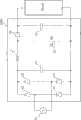
请参照图3,其为依据本发明的一实施例应用一电源转换器3000转换一交流电源SA的交流电来产生一直流电至一负载Rload的示意图。电源转换器3000包含有一无桥式(bridgeless)交换电路3100以及一开关控制电路3200。无桥式交换电路3100依据一交流电(alternating current,AC)信号来产生一输出信号,且具有一第一开关元件SW1与一第二开关元件SW2,此外,无桥式交换电路3100之中大部分的电路与图2所示的无桥式交换电路2000大致相同,在此便不再赘述。开关控制电路3200包含有一电流产生元件3210以及一相位产生元件3220。Please refer to FIG. 3 , which is a schematic diagram of applying a power converter 3000 to convert the AC power of an AC power source SA to generate a DC power to a load Rload according to an embodiment of the present invention. The power converter 3000 includes a bridgeless switching circuit 3100 and a
电流产生元件3210会分别感测流经第一开关元件SW1的一第一电流I1以及流经第二开关元件SW2的一第二电流I2,并依据第一电流I1以及第二电流I2来产生一相位比较结果,在本实施例中,第一电流I1与第二电流I2会分别流经相对应的电阻R1与R2,并产生正比于第一电流I1与第二电流I2的电压VR1与VR2,电流产生元件3210便接收电压VR1与VR2来产生该相位比较结果;该相位比较结果包含有一第一比较结果CR1以及一第二比较结果CR2。相位产生元件3220依据一功率因子矫正信号PFC(由一外部电路所登供)以及该相位比较结果(亦即第一比较结果CR1以及第二比较结果CR2)来产生一第一控制信号S1以及一第二控制信号S2来分别控制第一开关元件SW1与第二开关元件SW2的导通状态。The
请注意,在此范例之中,相位产生元件3320所产生的第一控制信号S1以及第二控制信号S2不会让第一开关元件SW1以及第二开关元件SW2同时不导通,亦即,第一控制信号S1以及第二控制信号S2会同时开启第一开关元件SW1以及第二开关元件SW2的导通状态或是开启第一开关元件SW1以及第二开关元件SW2至少其中之一的导通状态。在电源转换器3000满载的状态之下,第一开关元件SW1(或第二开关元件SW2)在导通时的压降与其在未导通时寄生二级管的压降所造成的功率消耗差异并不大;然而,在半载或是轻载状态之下,相比较图2所示的公知无桥式交换电路2000,无桥式交换电路3100在导通路径上不会遭遇到第一开关元件SW1或第二开关元件SW2之中的寄生二级管D3或D4,而只会见到第一开关元件SW1或第二开关元件SW2源极-汲极端的压降,在半载或是轻载状态等电流较小的工作情况之下,开关元件SW1或SW2源极-汲极端的压降所造成的功率损失会小于其中寄生二级管D3或D4运作时的功率损失。此外,第一开关元件SW1与第二开关元件SW2因开关所损失的功率也会随着开关次数的减少而降低。是故电源转换器3000在最终转换后传送给负载Rload的电压,会较图2所示的公知无桥式交换电路2000来得高,因此可有效地提高转换效率。Please note that in this example, the first control signal S1 and the second control signal S2 generated by the phase generating element 3320 will not make the first switching element SW1 and the second switching element SW2 non-conductive at the same time, that is, the first switching element SW1 and the second switching element SW2 will not be turned on simultaneously. A control signal S1 and a second control signal S2 simultaneously turn on the conduction state of the first switch element SW1 and the second switch element SW2 or turn on the conduction state of at least one of the first switch element SW1 and the second switch element SW2 . When the power converter 3000 is fully loaded, the difference in power consumption caused by the voltage drop of the first switch element SW1 (or the second switch element SW2) when it is turned on and the voltage drop of the parasitic diode when it is not turned on Not large; however, under half-load or light-load conditions, compared to the known bridgeless switching circuit 2000 shown in FIG. 2, the bridgeless switching circuit 3100 does not encounter the first switch on the conduction path The parasitic diode D3 or D4 in the element SW1 or the second switching element SW2, and only see the voltage drop of the source-drain terminal of the first switching element SW1 or the second switching element SW2, at half load or light load Under low current working conditions, such as low current, the power loss caused by the voltage drop at the source-drain terminal of the switching element SW1 or SW2 is smaller than the power loss when the parasitic diode D3 or D4 is in operation. In addition, the power loss due to the switching of the first switching element SW1 and the second switching element SW2 also decreases as the switching times decrease. Therefore, the voltage delivered to the load Rload by the power converter 3000 after the final conversion is higher than that of the known bridgeless switching circuit 2000 shown in FIG. 2 , so the conversion efficiency can be effectively improved.
请再参照图4,其为依据本发明的一实施例所实现的电流产生元件3210的结构示意图。电流产生元件3210包含有一第一比较器3211以及一第二比较器3212。第一比较器3211接收一第一参考电压VR1,并依据正比于第一电流I1的电压VS 1以及第一参考电压VR1来产生第一比较结果CR1;而第二比较器3212则接收一第二参考电压VR2,并依据正比于第二电流I2的电压VS2以及第二参考电压VR2来产生第二比较结果CR2。请再参照图5来进一步了解相位产生元件3220的运作与结构。图5为依据本发明的一实施例所实现的相位产生元件3220的结构示意图。相位产生元件3220包含有一磁滞(hysteresis)电路3221以及一决定电路3222。磁滞电路3221会依据该相位比较结果(亦即第一比较结果CR1以及第二比较结果CR2)之一变化状态来产生一相位信号SP。磁滞电路3221的应用可以确保在交流电源SA的交流电信号相位变化大小超过一预定门限时,才会输出相对应的相位信号SP,因此,即使第一比较结果CR1以及第二比较结果CR2因噪声信号等外在因素而有所变动时,磁滞电路3221仍可正确地输出相位信号SP。决定电路3222则会依据相位信号SP以及功率因子矫正信号PFC来产生第一控制信号S1以及第二控制信号S2。在此实施例中,决定电路3222包含有反向器INV1与INV2、OR逻辑门OR1与OR2。由图可知,反向器INV1与INV2会将相位信号SP反向放大之后,分别输入OR逻辑门OR1与OR2,而OR逻辑门OR1与OR2则同时接收功率因子矫正信号PFC,以产生第一控制信号S1以及第二控制信号S2。本领域的技术人员在参阅上述范例以及图5之后,应可轻易得知当功率因子矫正信号PFC指示为”开启”状态时,第一开关元件SW1与第二开关元件SW2均会呈现导通状态,而当功率因子矫正信号PFC指示为”关闭”状态时,第一开关元件SW1与第二开关元件SW2其中之一会依据磁滞电路3221所输出的相位信号SP而呈现导通状态,而另外一开关电路则会呈现不导通状态。如此一来,不但可以大幅减少开关元件SW1与SW2的开关次数,在电源转换器3000处理轻载或是满载时,由于其中的信号传导路径上不会见到开关元件SW1或SW2中的寄生二级管的压降而只有开关元件SW1或SW2的源极-漏极端的压降,是故其转换效率可被开关控制电路3200更进一步地加以提升。Please refer to FIG. 4 again, which is a schematic structural diagram of a
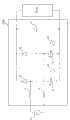
请参照图6,其为依据本发明的另一实施例应用一电源转换器6000转换交流电源SA的交流电来产生一直流电至负载Rload的示意图。电源转换器6000包含有与图3相同的无桥式交换电路3100以及开关控制电路3200,并另包含有一积分电路6300以及一噪声信号排除元件6400。积分电路6300用来依据交流电源SA的该交流电信号来产生一积分信号SI,在此实施例中,积分电路6300可应用简易的电容与电阻组合来加以实现,只要最终所输出的积分信号SI能反应出该交流电信号的绝对值大小即可。噪声信号排除元件6400则会依积分信号SI来产生一电压信号Vz,并依据相位产生元件3220所产生的相位信号SP来选择性地输出电压信号Vz作为第一参考电压VR1或是第二参考电压VR2。请参照图7来进一步了解噪声信号排除元件6400的结构与运作,图7为依据本发明的一实施例所实现的一噪声信号排除元件6400的结构示意图。噪声信号排除元件6400包含有一电压-电流转换器6410、一曾纳二级管(Zender diode)6420以及一辅助开关元件6430。电压-电流转换器具有用以接收积分信号SI的一输入端以及输出一参考电流的一输出端,其主要的用途在于将积分信号SI的电压转换为该参考电流,以便后续的处理。曾纳二级管(Zender diode)6420则具有耦接于电压-电流转换器6410的该输出端的一第一端以及耦接于一参考电压(在此实施例中,该参考电压为一接地电压)的一第二端,用以接收该参考电流并转换该参考电流为电压信号Vz。辅助开关元件6430具有用以接收电压信号Vz的一输入端、用以接收相位信号SP的一控制端以及耦接于电流产生元件3210的一第一输出端与一第二输出端,用以依据相位信号SP来选择性地将该输入端耦接至该第一输出端或者该第二输出端。由于曾纳二级管6420本身的电压-电流特性,当该参考电流过大时(亦即表示所输入的交流电信号过大时),其所输出的电压信号Vz仍会被限制在一预定范围之内,是故当交流电信号过大时,噪声信号排除元件6400仍会通过曾纳二级管6420的特性来提供一预定范围之内的第一参考电压VR1与第二参考电压VR2;而当交流电信号较小时,噪声信号排除元件6400也会输出适当大小的第一参考电压VR1与第二参考电压VR2来供电流产生元件3210使用,以维持相位检测的灵敏度。Please refer to FIG. 6 , which is a schematic diagram of applying a
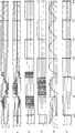
请再配合图6来参照图8,图8为依据本发明的一实施例所实现的电源转换器6000在一般运作时的部分信号时序图。由图8可知,当接收到交流电信号时,开关元件SW1与SW2会不停切换而产生电流I1与I2来对负载Rload充电,相位产生元件3220也会依据电流I1与I2的状态而产生相位信号SP,积分电路6300则会依该交流电信号的大小来产生整流后的积分信号SI给开关控制电路3200,积分信号SI可反应出该交流电信号的绝对值大小,是故噪声信号排除元件6400可依据积分信号SI来提供适当大小的第一参考电压VR1与第二参考电压VR2来给电流产生元件3210作为相位检测之用。当相位信号SP为高电位时,第一控制信号S1也会维持在高电位而将第一开关元件SW1持续在导通状态,而第二控制信号S2则会依据功率因子矫正信号PFC而开启或关闭第二开关元件SW2以提高转换效率;反之,当相位信号SP为低电位时,第二控制信号S2会维持在高电位而持续将第二开关元件SW2导通,第一控制信号S1则会依据功率因子矫正信号PFC而开启或关闭第一开关元件SW1。相较于公知技术,本发明中的第一控制信号S1以及第二控制信号S2不会让第一开关元件S1以及第二开关元件S2同时呈现不导通的状态,如此一来,可避免路径上不必要的压降,并可降低对开关元件的开关次数来以减少功率消耗,进而提升转换效率。Please refer to FIG. 8 in conjunction with FIG. 6 . FIG. 8 is a partial signal timing diagram of the
请再配合图8来参照图9,图9为依据本发明的一实施例所实现的电源转换器6000在间歇模式(hick-up mode)的部分信号时序图。当电源转换器6000进入间歇模式时,其所接收到的交流电信号会间歇性地休止,然而,由图9可知,即使在休止期间,第一开关元件SW1以及第二开关元件SW2仍会有微小的电流通过,噪声信号排除元件6400也会输出较小的电压信号Vz来作为第一参考电压VR1或是第二参考电压VR2,以便由后续的电流产生元件3210以及相位产生元件3220正确地产生第一比较结果CR1、第二比较结果CR2以及相位信号SP,并将相位信号SP维持在正确的相位,然而,传统的无桥式交换电路的控制方法均是将第一开关元件SW1以及第二开关元件SW2同时开启或关闭,是故无法在导通少量电流时清楚定义其相位关系,而电源转换器6000则在各种情况之下,均可维持准确的相位关系,使得后续的处理电路可以更加轻易地工作。Please refer to FIG. 9 in conjunction with FIG. 8 . FIG. 9 is a partial signal timing diagram of the
总结来说,本发明提供了一无桥式交换电路与电源转换器的开关控制电路以及相关方法,通过控制该无桥式交换电路中第一开关元件与一第二开关元件的导通状态,能有效地提升电源转换效率。In summary, the present invention provides a bridgeless switching circuit and a switch control circuit of a power converter and a related method. By controlling the conduction state of a first switching element and a second switching element in the bridgeless switching circuit, Can effectively improve power conversion efficiency.
以上所述仅为本发明的优选实施例,凡依本发明权利要求所做的均等变化与修饰,皆应属本发明的涵盖范围。The above descriptions are only preferred embodiments of the present invention, and all equivalent changes and modifications made according to the claims of the present invention shall fall within the scope of the present invention.
Claims (25)
Translated fromChineseApplications Claiming Priority (2)
| Application Number | Priority Date | Filing Date | Title |
|---|---|---|---|
| TW100109686 | 2011-03-22 | ||
| TW100109686ATWI439021B (en) | 2011-03-22 | 2011-03-22 | Switch control circuit and control method for bridgeless switching circuit, power converter and power control method |
Publications (2)
| Publication Number | Publication Date |
|---|---|
| CN102694476Atrue CN102694476A (en) | 2012-09-26 |
| CN102694476B CN102694476B (en) | 2015-01-14 |
Family
ID=46859786
Family Applications (1)
| Application Number | Title | Priority Date | Filing Date |
|---|---|---|---|
| CN201110156183.2AActiveCN102694476B (en) | 2011-03-22 | 2011-06-08 | Switch control circuit applied to bridgeless exchange circuit and control method |
Country Status (3)
| Country | Link |
|---|---|
| US (1) | US8564993B2 (en) |
| CN (1) | CN102694476B (en) |
| TW (1) | TWI439021B (en) |
Cited By (1)
| Publication number | Priority date | Publication date | Assignee | Title |
|---|---|---|---|---|
| CN110445402A (en)* | 2019-07-29 | 2019-11-12 | 深圳市航嘉驰源电气股份有限公司 | Active diode circuit and ac-dc power conversion circuit |
Families Citing this family (9)
| Publication number | Priority date | Publication date | Assignee | Title |
|---|---|---|---|---|
| CN103809007A (en)* | 2012-11-13 | 2014-05-21 | 中兴通讯股份有限公司 | Device and method for inductive current sampling of bridge-free PFC circuit |
| JP6089677B2 (en)* | 2012-12-19 | 2017-03-08 | 富士通株式会社 | Power supply |
| CN103887962B (en)* | 2012-12-20 | 2016-08-17 | Tdk株式会社 | Circuit of power factor correction |
| US9431896B2 (en) | 2013-12-19 | 2016-08-30 | Texas Instruments Incorporated | Apparatus and method for zero voltage switching in bridgeless totem pole power factor correction converter |
| US10284112B2 (en)* | 2017-05-09 | 2019-05-07 | City University Of Hong Kong | Circuit arrangement for use in a power conversion stage and a method of controlling a power conversion stage |
| JP6936693B2 (en)* | 2017-10-23 | 2021-09-22 | 株式会社Soken | Power converter |
| US10944337B2 (en) | 2017-12-15 | 2021-03-09 | Texas Instruments Incorporated | Adaptive zero voltage switching (ZVS) loss detection for power converters |
| TWI690143B (en)* | 2019-04-02 | 2020-04-01 | 瑞昱半導體股份有限公司 | Voltage converter |
| US11418125B2 (en) | 2019-10-25 | 2022-08-16 | The Research Foundation For The State University Of New York | Three phase bidirectional AC-DC converter with bipolar voltage fed resonant stages |
Citations (7)
| Publication number | Priority date | Publication date | Assignee | Title |
|---|---|---|---|---|
| US6411535B1 (en)* | 2001-03-29 | 2002-06-25 | Emc Corporation | Power factor correction circuit with integral bridge function |
| CN1864319A (en)* | 2003-10-01 | 2006-11-15 | 国际整流器公司 | Bridgeless boost converter with pfc circuit |
| CN101064433A (en)* | 2006-04-28 | 2007-10-31 | 高效电子股份有限公司 | Bridgeless power factor correction circuit and its control method |
| CN101151791A (en)* | 2005-03-31 | 2008-03-26 | 国际整流器公司 | Bridgeless boost converter with PFC circuit |
| CN101604913A (en)* | 2008-04-11 | 2009-12-16 | 崇贸科技股份有限公司 | Bridgeless power converter with power factor correction |
| WO2010124637A1 (en)* | 2009-04-28 | 2010-11-04 | 珠海格力电器股份有限公司 | Single-phase bridgeless power factor correction circuit |
| CN101931319A (en)* | 2009-06-08 | 2010-12-29 | 康舒科技股份有限公司 | Bridgeless Power Factor Correction Circuit |
Family Cites Families (3)
| Publication number | Priority date | Publication date | Assignee | Title |
|---|---|---|---|---|
| TWI384736B (en)* | 2009-07-15 | 2013-02-01 | Delta Eletronics Inc | Bridgeless pfc circuit system having current sensing circuit and method thereof |
| US8717791B2 (en)* | 2009-09-30 | 2014-05-06 | Astec International Limited | Bridgeless boost PFC circuits and systems |
| US8482942B2 (en)* | 2010-08-26 | 2013-07-09 | Fairchild Semiconductor Corporation | Method and apparatus for bridgeless power factor correction |
- 2011
- 2011-03-22TWTW100109686Apatent/TWI439021B/enactive
- 2011-06-08CNCN201110156183.2Apatent/CN102694476B/enactiveActive
- 2011-08-04USUS13/198,710patent/US8564993B2/enactiveActive
Patent Citations (7)
| Publication number | Priority date | Publication date | Assignee | Title |
|---|---|---|---|---|
| US6411535B1 (en)* | 2001-03-29 | 2002-06-25 | Emc Corporation | Power factor correction circuit with integral bridge function |
| CN1864319A (en)* | 2003-10-01 | 2006-11-15 | 国际整流器公司 | Bridgeless boost converter with pfc circuit |
| CN101151791A (en)* | 2005-03-31 | 2008-03-26 | 国际整流器公司 | Bridgeless boost converter with PFC circuit |
| CN101064433A (en)* | 2006-04-28 | 2007-10-31 | 高效电子股份有限公司 | Bridgeless power factor correction circuit and its control method |
| CN101604913A (en)* | 2008-04-11 | 2009-12-16 | 崇贸科技股份有限公司 | Bridgeless power converter with power factor correction |
| WO2010124637A1 (en)* | 2009-04-28 | 2010-11-04 | 珠海格力电器股份有限公司 | Single-phase bridgeless power factor correction circuit |
| CN101931319A (en)* | 2009-06-08 | 2010-12-29 | 康舒科技股份有限公司 | Bridgeless Power Factor Correction Circuit |
Cited By (1)
| Publication number | Priority date | Publication date | Assignee | Title |
|---|---|---|---|---|
| CN110445402A (en)* | 2019-07-29 | 2019-11-12 | 深圳市航嘉驰源电气股份有限公司 | Active diode circuit and ac-dc power conversion circuit |
Also Published As
| Publication number | Publication date |
|---|---|
| US8564993B2 (en) | 2013-10-22 |
| TW201240292A (en) | 2012-10-01 |
| CN102694476B (en) | 2015-01-14 |
| TWI439021B (en) | 2014-05-21 |
| US20120243275A1 (en) | 2012-09-27 |
Similar Documents
| Publication | Publication Date | Title |
|---|---|---|
| CN102694476B (en) | Switch control circuit applied to bridgeless exchange circuit and control method | |
| US8953347B2 (en) | Capacitor discharging circuit and power converter | |
| US9742264B2 (en) | Boost inductor demagnetization detection for bridgeless boost PFC converter operating in boundary-conduction mode | |
| CN107086793B (en) | A Dynamic Compensation Control Circuit for Synchronous Rectification Power Converter | |
| TWI436571B (en) | Control circuit and synchronous rectifier circuit using the same | |
| US8837174B2 (en) | Switching power-supply apparatus including switching elements having a low threshold voltage | |
| TWI454036B (en) | Bridge rectifier for a pfc power converter | |
| US20090230929A1 (en) | Bridgeless pfc circuit for crm and controlling method thereof | |
| KR100829121B1 (en) | Power Factor Correction Circuit for Single Power Operation in BCM Mode | |
| JP6859034B2 (en) | Circuits and methods for synchronous rectification in resonant transducers | |
| CN109450256B (en) | A Quasi-Resonant Power Controller | |
| TWI408898B (en) | Compensation device for synchronous rectifier control and method thereof | |
| CN106685242A (en) | Single-stage AC-DC converter | |
| CN111628654B (en) | Switching power supply circuit | |
| CN106026719B (en) | P-SSHI active rectifying circuits and self-supplied electronic equipment | |
| TW202349837A (en) | Power supply device with fast discharge function | |
| CN117543977A (en) | An adaptive zero-crossing detection circuit and BUCK-type switching power supply | |
| CN206962707U (en) | A kind of dynamic compesated control circuit for synchronous rectification power inverter | |
| CN108418433A (en) | A kind of LLC resonant converter and its control circuit, resonant current sampling circuit | |
| TWI586092B (en) | Single stage AC to DC converter | |
| KR101776617B1 (en) | Isolated bridgeless power factor corrector converter | |
| US20240421703A1 (en) | Bidirectional bridgeless pfc circuit | |
| US20140002035A1 (en) | Common-core power factor correction resonant converter | |
| CN101534064A (en) | Power-taking circuit of AC-DC converter | |
| CN112134459B (en) | Synchronous converter control circuit |
Legal Events
| Date | Code | Title | Description |
|---|---|---|---|
| C06 | Publication | ||
| PB01 | Publication | ||
| C10 | Entry into substantive examination | ||
| SE01 | Entry into force of request for substantive examination | ||
| C14 | Grant of patent or utility model | ||
| GR01 | Patent grant |