CN102694001A - Organic electroluminescence display and method of manufacturing the same - Google Patents
Organic electroluminescence display and method of manufacturing the sameDownload PDFInfo
- Publication number
- CN102694001A CN102694001ACN2012100637769ACN201210063776ACN102694001ACN 102694001 ACN102694001 ACN 102694001ACN 2012100637769 ACN2012100637769 ACN 2012100637769ACN 201210063776 ACN201210063776 ACN 201210063776ACN 102694001 ACN102694001 ACN 102694001A
- Authority
- CN
- China
- Prior art keywords
- organic
- emitting layer
- layer
- display device
- transport layer
- Prior art date
- Legal status (The legal status is an assumption and is not a legal conclusion. Google has not performed a legal analysis and makes no representation as to the accuracy of the status listed.)
- Pending
Links
- 238000004519manufacturing processMethods0.000titleclaimsabstractdescription25
- 238000005401electroluminescenceMethods0.000titleclaimsdescription194
- 238000002347injectionMethods0.000claimsabstractdescription92
- 239000007924injectionSubstances0.000claimsabstractdescription92
- 239000000758substrateSubstances0.000claimsabstractdescription38
- 239000003086colorantSubstances0.000claimsabstractdescription36
- 239000000463materialSubstances0.000claimsdescription105
- 238000000034methodMethods0.000claimsdescription84
- 230000005525hole transportEffects0.000claimsdescription34
- 229910052751metalInorganic materials0.000claimsdescription22
- 239000002184metalSubstances0.000claimsdescription20
- 238000000576coating methodMethods0.000claimsdescription19
- 238000001704evaporationMethods0.000claimsdescription19
- 238000007639printingMethods0.000claimsdescription11
- 230000008020evaporationEffects0.000claimsdescription8
- 238000004528spin coatingMethods0.000claimsdescription5
- 238000007646gravure printingMethods0.000claimsdescription4
- 238000007644letterpress printingMethods0.000claims1
- 238000000520microinjectionMethods0.000claims1
- 238000007645offset printingMethods0.000claims1
- 239000007921spraySubstances0.000claims1
- 238000005507sprayingMethods0.000claims1
- 238000005265energy consumptionMethods0.000abstractdescription12
- 239000010410layerSubstances0.000description261
- -1polyethylene terephthalatePolymers0.000description98
- 239000010408filmSubstances0.000description33
- 150000001875compoundsChemical class0.000description30
- 238000005192partitionMethods0.000description21
- 238000010438heat treatmentMethods0.000description17
- 125000003118aryl groupChemical group0.000description16
- 239000011241protective layerSubstances0.000description15
- 238000007789sealingMethods0.000description14
- 239000012044organic layerSubstances0.000description13
- 239000010409thin filmSubstances0.000description11
- QVGXLLKOCUKJST-UHFFFAOYSA-Natomic oxygenChemical compound[O]QVGXLLKOCUKJST-UHFFFAOYSA-N0.000description10
- 229910052760oxygenInorganic materials0.000description10
- 239000001301oxygenSubstances0.000description10
- 229910045601alloyInorganic materials0.000description9
- 239000000956alloySubstances0.000description9
- 125000002029aromatic hydrocarbon groupChemical group0.000description9
- 239000002861polymer materialSubstances0.000description9
- 239000011347resinSubstances0.000description9
- 229920005989resinPolymers0.000description9
- 125000000623heterocyclic groupChemical group0.000description8
- 239000000126substanceSubstances0.000description8
- 239000011777magnesiumSubstances0.000description7
- 239000011159matrix materialSubstances0.000description7
- 239000002019doping agentSubstances0.000description6
- 238000001035dryingMethods0.000description6
- 239000011810insulating materialSubstances0.000description6
- BASFCYQUMIYNBI-UHFFFAOYSA-NplatinumChemical compound[Pt]BASFCYQUMIYNBI-UHFFFAOYSA-N0.000description6
- 229920000642polymerPolymers0.000description6
- 229920000123polythiophenePolymers0.000description6
- 230000035945sensitivityEffects0.000description6
- 230000000007visual effectEffects0.000description6
- 230000005457Black-body radiationEffects0.000description5
- 229910052782aluminiumInorganic materials0.000description5
- 230000009286beneficial effectEffects0.000description5
- 230000015572biosynthetic processEffects0.000description5
- 229920001940conductive polymerPolymers0.000description5
- 230000007423decreaseEffects0.000description5
- 239000011521glassSubstances0.000description5
- 229920000767polyanilinePolymers0.000description5
- VYPSYNLAJGMNEJ-UHFFFAOYSA-Nsilicon dioxideInorganic materialsO=[Si]=OVYPSYNLAJGMNEJ-UHFFFAOYSA-N0.000description5
- 125000001424substituent groupChemical group0.000description5
- UWRZIZXBOLBCON-VOTSOKGWSA-N(e)-2-phenylethenamineChemical classN\C=C\C1=CC=CC=C1UWRZIZXBOLBCON-VOTSOKGWSA-N0.000description4
- OKTJSMMVPCPJKN-UHFFFAOYSA-NCarbonChemical compound[C]OKTJSMMVPCPJKN-UHFFFAOYSA-N0.000description4
- UFWIBTONFRDIAS-UHFFFAOYSA-NNaphthaleneChemical compoundC1=CC=CC2=CC=CC=C21UFWIBTONFRDIAS-UHFFFAOYSA-N0.000description4
- BQCADISMDOOEFD-UHFFFAOYSA-NSilverChemical compound[Ag]BQCADISMDOOEFD-UHFFFAOYSA-N0.000description4
- YTPLMLYBLZKORZ-UHFFFAOYSA-NThiopheneChemical compoundC=1C=CSC=1YTPLMLYBLZKORZ-UHFFFAOYSA-N0.000description4
- 239000012790adhesive layerSubstances0.000description4
- XAGFODPZIPBFFR-UHFFFAOYSA-NaluminiumChemical compound[Al]XAGFODPZIPBFFR-UHFFFAOYSA-N0.000description4
- 229910021417amorphous siliconInorganic materials0.000description4
- MWPLVEDNUUSJAV-UHFFFAOYSA-NanthraceneChemical compoundC1=CC=CC2=CC3=CC=CC=C3C=C21MWPLVEDNUUSJAV-UHFFFAOYSA-N0.000description4
- 239000003990capacitorSubstances0.000description4
- 229910052799carbonInorganic materials0.000description4
- 238000005229chemical vapour depositionMethods0.000description4
- 239000011651chromiumSubstances0.000description4
- 239000002131composite materialSubstances0.000description4
- 230000002708enhancing effectEffects0.000description4
- 239000010931goldSubstances0.000description4
- 150000002430hydrocarbonsChemical group0.000description4
- 229910052749magnesiumInorganic materials0.000description4
- 150000002739metalsChemical class0.000description4
- 239000011259mixed solutionSubstances0.000description4
- 238000009832plasma treatmentMethods0.000description4
- 239000004332silverSubstances0.000description4
- UHOVQNZJYSORNB-UHFFFAOYSA-NBenzeneChemical compoundC1=CC=CC=C1UHOVQNZJYSORNB-UHFFFAOYSA-N0.000description3
- WHXSMMKQMYFTQS-UHFFFAOYSA-NLithiumChemical compound[Li]WHXSMMKQMYFTQS-UHFFFAOYSA-N0.000description3
- FYYHWMGAXLPEAU-UHFFFAOYSA-NMagnesiumChemical compound[Mg]FYYHWMGAXLPEAU-UHFFFAOYSA-N0.000description3
- PXHVJJICTQNCMI-UHFFFAOYSA-NNickelChemical compound[Ni]PXHVJJICTQNCMI-UHFFFAOYSA-N0.000description3
- KDLHZDBZIXYQEI-UHFFFAOYSA-NPalladiumChemical compound[Pd]KDLHZDBZIXYQEI-UHFFFAOYSA-N0.000description3
- YXFVVABEGXRONW-UHFFFAOYSA-NTolueneChemical compoundCC1=CC=CC=C1YXFVVABEGXRONW-UHFFFAOYSA-N0.000description3
- DGEZNRSVGBDHLK-UHFFFAOYSA-N[1,10]phenanthrolineChemical compoundC1=CN=C2C3=NC=CC=C3C=CC2=C1DGEZNRSVGBDHLK-UHFFFAOYSA-N0.000description3
- 150000004982aromatic aminesChemical group0.000description3
- 239000011575calciumSubstances0.000description3
- 125000000609carbazolyl groupChemical groupC1(=CC=CC=2C3=CC=CC=C3NC12)*0.000description3
- 125000004432carbon atomChemical groupC*0.000description3
- 229920000547conjugated polymerPolymers0.000description3
- 238000010586diagramMethods0.000description3
- 239000006185dispersionSubstances0.000description3
- 230000005284excitationEffects0.000description3
- RAXXELZNTBOGNW-UHFFFAOYSA-NimidazoleNatural productsC1=CNC=N1RAXXELZNTBOGNW-UHFFFAOYSA-N0.000description3
- 229910052744lithiumInorganic materials0.000description3
- 239000000203mixtureSubstances0.000description3
- QJGQUHMNIGDVPM-UHFFFAOYSA-Nnitrogen groupChemical group[N]QJGQUHMNIGDVPM-UHFFFAOYSA-N0.000description3
- 239000011368organic materialSubstances0.000description3
- 239000003960organic solventSubstances0.000description3
- 230000035699permeabilityEffects0.000description3
- 229920003227poly(N-vinyl carbazole)Polymers0.000description3
- 230000009467reductionEffects0.000description3
- 235000012239silicon dioxideNutrition0.000description3
- 229910052709silverInorganic materials0.000description3
- 239000007787solidSubstances0.000description3
- 239000002904solventSubstances0.000description3
- CXWXQJXEFPUFDZ-UHFFFAOYSA-NtetralinChemical compoundC1=CC=C2CCCCC2=C1CXWXQJXEFPUFDZ-UHFFFAOYSA-N0.000description3
- 238000002834transmittanceMethods0.000description3
- QNLZIZAQLLYXTC-UHFFFAOYSA-N1,2-dimethylnaphthaleneChemical compoundC1=CC=CC2=C(C)C(C)=CC=C21QNLZIZAQLLYXTC-UHFFFAOYSA-N0.000description2
- NPDIDUXTRAITDE-UHFFFAOYSA-N1-methyl-3-phenylbenzeneChemical groupCC1=CC=CC(C=2C=CC=CC=2)=C1NPDIDUXTRAITDE-UHFFFAOYSA-N0.000description2
- QPUYECUOLPXSFR-UHFFFAOYSA-N1-methylnaphthaleneChemical compoundC1=CC=C2C(C)=CC=CC2=C1QPUYECUOLPXSFR-UHFFFAOYSA-N0.000description2
- HBEDSQVIWPRPAY-UHFFFAOYSA-N2,3-dihydrobenzofuranChemical compoundC1=CC=C2OCCC2=C1HBEDSQVIWPRPAY-UHFFFAOYSA-N0.000description2
- ZZLCFHIKESPLTH-UHFFFAOYSA-N4-MethylbiphenylChemical groupC1=CC(C)=CC=C1C1=CC=CC=C1ZZLCFHIKESPLTH-UHFFFAOYSA-N0.000description2
- UJOBWOGCFQCDNV-UHFFFAOYSA-N9H-carbazoleChemical compoundC1=CC=C2C3=CC=CC=C3NC2=C1UJOBWOGCFQCDNV-UHFFFAOYSA-N0.000description2
- PAYRUJLWNCNPSJ-UHFFFAOYSA-NAnilineChemical compoundNC1=CC=CC=C1PAYRUJLWNCNPSJ-UHFFFAOYSA-N0.000description2
- KAKZBPTYRLMSJV-UHFFFAOYSA-NButadieneChemical compoundC=CC=CKAKZBPTYRLMSJV-UHFFFAOYSA-N0.000description2
- VYZAMTAEIAYCRO-UHFFFAOYSA-NChromiumChemical compound[Cr]VYZAMTAEIAYCRO-UHFFFAOYSA-N0.000description2
- 229910019015Mg-AgInorganic materials0.000description2
- CTQNGGLPUBDAKN-UHFFFAOYSA-NO-XyleneChemical compoundCC1=CC=CC=C1CCTQNGGLPUBDAKN-UHFFFAOYSA-N0.000description2
- 229920001609Poly(3,4-ethylenedioxythiophene)Polymers0.000description2
- JUJWROOIHBZHMG-UHFFFAOYSA-NPyridineChemical compoundC1=CC=NC=C1JUJWROOIHBZHMG-UHFFFAOYSA-N0.000description2
- KAESVJOAVNADME-UHFFFAOYSA-NPyrroleChemical compoundC=1C=CNC=1KAESVJOAVNADME-UHFFFAOYSA-N0.000description2
- SMWDFEZZVXVKRB-UHFFFAOYSA-NQuinolineChemical compoundN1=CC=CC2=CC=CC=C21SMWDFEZZVXVKRB-UHFFFAOYSA-N0.000description2
- DZBUGLKDJFMEHC-UHFFFAOYSA-NacridineChemical compoundC1=CC=CC2=CC3=CC=CC=C3N=C21DZBUGLKDJFMEHC-UHFFFAOYSA-N0.000description2
- 125000003342alkenyl groupChemical group0.000description2
- 125000000217alkyl groupChemical group0.000description2
- 125000003277amino groupChemical group0.000description2
- RDOXTESZEPMUJZ-UHFFFAOYSA-NanisoleChemical compoundCOC1=CC=CC=C1RDOXTESZEPMUJZ-UHFFFAOYSA-N0.000description2
- 150000001454anthracenesChemical class0.000description2
- 230000004888barrier functionEffects0.000description2
- 239000002585baseSubstances0.000description2
- 229910052792caesiumInorganic materials0.000description2
- TVFDJXOCXUVLDH-UHFFFAOYSA-Ncaesium atomChemical compound[Cs]TVFDJXOCXUVLDH-UHFFFAOYSA-N0.000description2
- 229910052791calciumInorganic materials0.000description2
- 125000002915carbonyl groupChemical group[*:2]C([*:1])=O0.000description2
- 229910052681coesiteInorganic materials0.000description2
- 239000010949copperSubstances0.000description2
- 229910052906cristobaliteInorganic materials0.000description2
- JHIVVAPYMSGYDF-UHFFFAOYSA-NcyclohexanoneChemical compoundO=C1CCCCC1JHIVVAPYMSGYDF-UHFFFAOYSA-N0.000description2
- HHNHBFLGXIUXCM-GFCCVEGCSA-NcyclohexylbenzeneChemical compound[CH]1CCCC[C@@H]1C1=CC=CC=C1HHNHBFLGXIUXCM-GFCCVEGCSA-N0.000description2
- 239000000412dendrimerSubstances0.000description2
- 230000006866deteriorationEffects0.000description2
- TXCDCPKCNAJMEE-UHFFFAOYSA-NdibenzofuranChemical groupC1=CC=C2C3=CC=CC=C3OC2=C1TXCDCPKCNAJMEE-UHFFFAOYSA-N0.000description2
- QDOXWKRWXJOMAK-UHFFFAOYSA-Ndichromium trioxideChemical compoundO=[Cr]O[Cr]=OQDOXWKRWXJOMAK-UHFFFAOYSA-N0.000description2
- 238000009792diffusion processMethods0.000description2
- DMBHHRLKUKUOEG-UHFFFAOYSA-NdiphenylamineChemical compoundC=1C=CC=CC=1NC1=CC=CC=C1DMBHHRLKUKUOEG-UHFFFAOYSA-N0.000description2
- 239000002612dispersion mediumSubstances0.000description2
- 230000005684electric fieldEffects0.000description2
- NIHNNTQXNPWCJQ-UHFFFAOYSA-NfluoreneChemical compoundC1=CC=C2CC3=CC=CC=C3C2=C1NIHNNTQXNPWCJQ-UHFFFAOYSA-N0.000description2
- 150000008376fluorenonesChemical class0.000description2
- 150000002222fluorine compoundsChemical class0.000description2
- PCHJSUWPFVWCPO-UHFFFAOYSA-NgoldChemical compound[Au]PCHJSUWPFVWCPO-UHFFFAOYSA-N0.000description2
- 229910052737goldInorganic materials0.000description2
- 230000005283ground stateEffects0.000description2
- 125000004435hydrogen atomChemical group[H]*0.000description2
- UEEXRMUCXBPYOV-UHFFFAOYSA-Niridium;2-phenylpyridineChemical compound[Ir].C1=CC=CC=C1C1=CC=CC=N1.C1=CC=CC=C1C1=CC=CC=N1.C1=CC=CC=C1C1=CC=CC=N1UEEXRMUCXBPYOV-UHFFFAOYSA-N0.000description2
- 238000010030laminatingMethods0.000description2
- 229910044991metal oxideInorganic materials0.000description2
- 150000004706metal oxidesChemical class0.000description2
- 229910052757nitrogenInorganic materials0.000description2
- 150000002916oxazolesChemical class0.000description2
- 230000000737periodic effectEffects0.000description2
- 125000002080perylenyl groupChemical groupC1(=CC=C2C=CC=C3C4=CC=CC5=CC=CC(C1=C23)=C45)*0.000description2
- CSHWQDPOILHKBI-UHFFFAOYSA-NperyreneNatural productsC1=CC(C2=CC=CC=3C2=C2C=CC=3)=C3C2=CC=CC3=C1CSHWQDPOILHKBI-UHFFFAOYSA-N0.000description2
- 239000000049pigmentSubstances0.000description2
- 229910052697platinumInorganic materials0.000description2
- 229920003229poly(methyl methacrylate)Polymers0.000description2
- 229920000553poly(phenylenevinylene)Polymers0.000description2
- 229920000139polyethylene terephthalatePolymers0.000description2
- 239000005020polyethylene terephthalateSubstances0.000description2
- 229920002098polyfluorenePolymers0.000description2
- 239000004926polymethyl methacrylateSubstances0.000description2
- 229920000128polypyrrolePolymers0.000description2
- 150000004032porphyrinsChemical class0.000description2
- UOHMMEJUHBCKEE-UHFFFAOYSA-NprehniteneChemical compoundCC1=CC=C(C)C(C)=C1CUOHMMEJUHBCKEE-UHFFFAOYSA-N0.000description2
- BBEAQIROQSPTKN-UHFFFAOYSA-NpyreneChemical compoundC1=CC=C2C=CC3=CC=CC4=CC=C1C2=C43BBEAQIROQSPTKN-UHFFFAOYSA-N0.000description2
- 239000010453quartzSubstances0.000description2
- 125000002943quinolinyl groupChemical groupN1=C(C=CC2=CC=CC=C12)*0.000description2
- 230000004044responseEffects0.000description2
- 239000010948rhodiumSubstances0.000description2
- HQVNEWCFYHHQES-UHFFFAOYSA-Nsilicon nitrideChemical compoundN12[Si]34N5[Si]62N3[Si]51N64HQVNEWCFYHHQES-UHFFFAOYSA-N0.000description2
- 239000002356single layerSubstances0.000description2
- 239000000243solutionSubstances0.000description2
- 238000001228spectrumMethods0.000description2
- 235000021286stilbenesNutrition0.000description2
- 229910052682stishoviteInorganic materials0.000description2
- 238000003860storageMethods0.000description2
- PCCVSPMFGIFTHU-UHFFFAOYSA-NtetracyanoquinodimethaneChemical compoundN#CC(C#N)=C1C=CC(=C(C#N)C#N)C=C1PCCVSPMFGIFTHU-UHFFFAOYSA-N0.000description2
- 229930192474thiopheneNatural products0.000description2
- TVIVIEFSHFOWTE-UHFFFAOYSA-Ktri(quinolin-8-yloxy)alumaneChemical compound[Al+3].C1=CN=C2C([O-])=CC=CC2=C1.C1=CN=C2C([O-])=CC=CC2=C1.C1=CN=C2C([O-])=CC=CC2=C1TVIVIEFSHFOWTE-UHFFFAOYSA-K0.000description2
- 150000003852triazolesChemical class0.000description2
- 229910052905tridymiteInorganic materials0.000description2
- XLYOFNOQVPJJNP-UHFFFAOYSA-NwaterSubstancesOXLYOFNOQVPJJNP-UHFFFAOYSA-N0.000description2
- 239000008096xyleneSubstances0.000description2
- OSITUIQNHIARIW-UHFFFAOYSA-N1,2,3-trimethylbenzene;1,2,4-trimethylbenzeneChemical compoundCC1=CC=C(C)C(C)=C1.CC1=CC=CC(C)=C1COSITUIQNHIARIW-UHFFFAOYSA-N0.000description1
- WZEYZMKZKQPXSX-UHFFFAOYSA-N1,3,5-trimethylbenzeneChemical compoundCC1=CC(C)=CC(C)=C1.CC1=CC(C)=CC(C)=C1WZEYZMKZKQPXSX-UHFFFAOYSA-N0.000description1
- YZVWKHVRBDQPMQ-UHFFFAOYSA-N1-aminopyreneChemical classC1=C2C(N)=CC=C(C=C3)C2=C2C3=CC=CC2=C1YZVWKHVRBDQPMQ-UHFFFAOYSA-N0.000description1
- SJADXKHSFIMCRC-UHFFFAOYSA-N1-n,1-n,4-n,4-n-tetrakis(4-methylphenyl)benzene-1,4-diamineChemical compoundC1=CC(C)=CC=C1N(C=1C=CC(=CC=1)N(C=1C=CC(C)=CC=1)C=1C=CC(C)=CC=1)C1=CC=C(C)C=C1SJADXKHSFIMCRC-UHFFFAOYSA-N0.000description1
- 1250000016371-naphthyl groupChemical group[H]C1=C([H])C([H])=C2C(*)=C([H])C([H])=C([H])C2=C1[H]0.000description1
- RUFPHBVGCFYCNW-UHFFFAOYSA-N1-naphthylamineChemical classC1=CC=C2C(N)=CC=CC2=C1RUFPHBVGCFYCNW-UHFFFAOYSA-N0.000description1
- LIWRTHVZRZXVFX-UHFFFAOYSA-N1-phenyl-3-propan-2-ylbenzeneChemical groupCC(C)C1=CC=CC(C=2C=CC=CC=2)=C1LIWRTHVZRZXVFX-UHFFFAOYSA-N0.000description1
- PMPBFICDXLLSRM-UHFFFAOYSA-N1-propan-2-ylnaphthaleneChemical compoundC1=CC=C2C(C(C)C)=CC=CC2=C1PMPBFICDXLLSRM-UHFFFAOYSA-N0.000description1
- 1250000014621-pyrrolyl groupChemical group[*]N1C([H])=C([H])C([H])=C1[H]0.000description1
- IXHWGNYCZPISET-UHFFFAOYSA-N2-[4-(dicyanomethylidene)-2,3,5,6-tetrafluorocyclohexa-2,5-dien-1-ylidene]propanedinitrileChemical compoundFC1=C(F)C(=C(C#N)C#N)C(F)=C(F)C1=C(C#N)C#NIXHWGNYCZPISET-UHFFFAOYSA-N0.000description1
- ACWRSZKNNOJCJE-UHFFFAOYSA-N2-n-naphthalen-1-yl-2-n-phenylbenzene-1,2-diamineChemical compoundNC1=CC=CC=C1N(C=1C2=CC=CC=C2C=CC=1)C1=CC=CC=C1ACWRSZKNNOJCJE-UHFFFAOYSA-N0.000description1
- 1250000016222-naphthyl groupChemical group[H]C1=C([H])C([H])=C2C([H])=C(*)C([H])=C([H])C2=C1[H]0.000description1
- 1250000039032-propenyl groupChemical group[H]C([*])([H])C([H])=C([H])[H]0.000description1
- 1250000041052-pyridyl groupChemical groupN1=C([*])C([H])=C([H])C([H])=C1[H]0.000description1
- 1250000003892-pyrrolyl groupChemical group[H]N1C([*])=C([H])C([H])=C1[H]0.000description1
- 1250000033493-pyridyl groupChemical groupN1=C([H])C([*])=C([H])C([H])=C1[H]0.000description1
- 1250000013973-pyrrolyl groupChemical group[H]N1C([H])=C([*])C([H])=C1[H]0.000description1
- MSHFRERJPWKJFX-UHFFFAOYSA-N4-Methoxybenzyl alcoholChemical compoundCOC1=CC=C(CO)C=C1MSHFRERJPWKJFX-UHFFFAOYSA-N0.000description1
- RMTFQLKKBBWGAH-UHFFFAOYSA-N4-methyl-n-(4-methylphenyl)-n-[4-(2-phenylethenyl)phenyl]anilineChemical compoundC1=CC(C)=CC=C1N(C=1C=CC(C=CC=2C=CC=CC=2)=CC=1)C1=CC=C(C)C=C1RMTFQLKKBBWGAH-UHFFFAOYSA-N0.000description1
- 1250000003394-pyridyl groupChemical groupN1=C([H])C([H])=C([*])C([H])=C1[H]0.000description1
- VIJYEGDOKCKUOL-UHFFFAOYSA-N9-phenylcarbazoleChemical compoundC1=CC=CC=C1N1C2=CC=CC=C2C2=CC=CC=C21VIJYEGDOKCKUOL-UHFFFAOYSA-N0.000description1
- 229910001316Ag alloyInorganic materials0.000description1
- 229910001148Al-Li alloyInorganic materials0.000description1
- IJGRMHOSHXDMSA-UHFFFAOYSA-NAtomic nitrogenChemical compoundN#NIJGRMHOSHXDMSA-UHFFFAOYSA-N0.000description1
- ZOXJGFHDIHLPTG-UHFFFAOYSA-NBoronChemical compound[B]ZOXJGFHDIHLPTG-UHFFFAOYSA-N0.000description1
- NLZUEZXRPGMBCV-UHFFFAOYSA-NButylhydroxytolueneChemical compoundCC1=CC(C(C)(C)C)=C(O)C(C(C)(C)C)=C1NLZUEZXRPGMBCV-UHFFFAOYSA-N0.000description1
- XMWRBQBLMFGWIX-UHFFFAOYSA-NC60 fullereneChemical classC12=C3C(C4=C56)=C7C8=C5C5=C9C%10=C6C6=C4C1=C1C4=C6C6=C%10C%10=C9C9=C%11C5=C8C5=C8C7=C3C3=C7C2=C1C1=C2C4=C6C4=C%10C6=C9C9=C%11C5=C5C8=C3C3=C7C1=C1C2=C4C6=C2C9=C5C3=C12XMWRBQBLMFGWIX-UHFFFAOYSA-N0.000description1
- OYPRJOBELJOOCE-UHFFFAOYSA-NCalciumChemical compound[Ca]OYPRJOBELJOOCE-UHFFFAOYSA-N0.000description1
- RYGMFSIKBFXOCR-UHFFFAOYSA-NCopperChemical compound[Cu]RYGMFSIKBFXOCR-UHFFFAOYSA-N0.000description1
- SNRUBQQJIBEYMU-UHFFFAOYSA-NDodecaneNatural productsCCCCCCCCCCCCSNRUBQQJIBEYMU-UHFFFAOYSA-N0.000description1
- UEXCJVNBTNXOEH-UHFFFAOYSA-NEthynylbenzeneChemical groupC#CC1=CC=CC=C1UEXCJVNBTNXOEH-UHFFFAOYSA-N0.000description1
- 229910052688GadoliniumInorganic materials0.000description1
- 229910000861Mg alloyInorganic materials0.000description1
- ZOKXTWBITQBERF-UHFFFAOYSA-NMolybdenumChemical compound[Mo]ZOKXTWBITQBERF-UHFFFAOYSA-N0.000description1
- 229920000557Nafion®Polymers0.000description1
- 239000004698PolyethyleneSubstances0.000description1
- 239000004642PolyimideSubstances0.000description1
- 229920000265PolyparaphenylenePolymers0.000description1
- 229920000292PolyquinolinePolymers0.000description1
- KJTLSVCANCCWHF-UHFFFAOYSA-NRutheniumChemical compound[Ru]KJTLSVCANCCWHF-UHFFFAOYSA-N0.000description1
- 229910004298SiO 2Inorganic materials0.000description1
- PJANXHGTPQOBST-VAWYXSNFSA-NStilbeneNatural productsC=1C=CC=CC=1/C=C/C1=CC=CC=C1PJANXHGTPQOBST-VAWYXSNFSA-N0.000description1
- SLGBZMMZGDRARJ-UHFFFAOYSA-NTriphenyleneNatural productsC1=CC=C2C3=CC=CC=C3C3=CC=CC=C3C2=C1SLGBZMMZGDRARJ-UHFFFAOYSA-N0.000description1
- XLOMVQKBTHCTTD-UHFFFAOYSA-NZinc monoxideChemical compound[Zn]=OXLOMVQKBTHCTTD-UHFFFAOYSA-N0.000description1
- 238000010521absorption reactionMethods0.000description1
- CUJRVFIICFDLGR-UHFFFAOYSA-NacetylacetonateChemical compoundCC(=O)[CH-]C(C)=OCUJRVFIICFDLGR-UHFFFAOYSA-N0.000description1
- 150000001335aliphatic alkanesChemical class0.000description1
- 125000001931aliphatic groupChemical group0.000description1
- 229910052783alkali metalInorganic materials0.000description1
- 150000001340alkali metalsChemical class0.000description1
- 229910052784alkaline earth metalInorganic materials0.000description1
- 150000001342alkaline earth metalsChemical class0.000description1
- 125000003545alkoxy groupChemical group0.000description1
- 125000003282alkyl amino groupChemical group0.000description1
- 229910021431alpha silicon carbideInorganic materials0.000description1
- HSFWRNGVRCDJHI-UHFFFAOYSA-Nalpha-acetyleneNatural productsC#CHSFWRNGVRCDJHI-UHFFFAOYSA-N0.000description1
- 229920005603alternating copolymerPolymers0.000description1
- APLQAVQJYBLXDR-UHFFFAOYSA-Naluminum quinolineChemical compound[Al+3].N1=CC=CC2=CC=CC=C12.N1=CC=CC2=CC=CC=C12.N1=CC=CC2=CC=CC=C12APLQAVQJYBLXDR-UHFFFAOYSA-N0.000description1
- 150000001412aminesChemical class0.000description1
- 229910003481amorphous carbonInorganic materials0.000description1
- YUENFNPLGJCNRB-UHFFFAOYSA-Nanthracen-1-amineChemical classC1=CC=C2C=C3C(N)=CC=CC3=CC2=C1YUENFNPLGJCNRB-UHFFFAOYSA-N0.000description1
- 125000006615aromatic heterocyclic groupChemical group0.000description1
- 125000001691aryl alkyl amino groupChemical group0.000description1
- 125000001769aryl amino groupChemical group0.000description1
- 230000002238attenuated effectEffects0.000description1
- 229910052788bariumInorganic materials0.000description1
- DSAJWYNOEDNPEQ-UHFFFAOYSA-Nbarium atomChemical compound[Ba]DSAJWYNOEDNPEQ-UHFFFAOYSA-N0.000description1
- HFACYLZERDEVSX-UHFFFAOYSA-NbenzidineChemical compoundC1=CC(N)=CC=C1C1=CC=C(N)C=C1HFACYLZERDEVSX-UHFFFAOYSA-N0.000description1
- 125000001164benzothiazolyl groupChemical groupS1C(=NC2=C1C=CC=C2)*0.000description1
- 229910052790berylliumInorganic materials0.000description1
- ATBAMAFKBVZNFJ-UHFFFAOYSA-Nberyllium atomChemical compound[Be]ATBAMAFKBVZNFJ-UHFFFAOYSA-N0.000description1
- 125000006269biphenyl-2-yl groupChemical group[H]C1=C([H])C([H])=C(C([H])=C1[H])C1=C(*)C([H])=C([H])C([H])=C1[H]0.000description1
- 125000006268biphenyl-3-yl groupChemical group[H]C1=C([H])C([H])=C(C([H])=C1[H])C1=C([H])C(*)=C([H])C([H])=C1[H]0.000description1
- 125000000319biphenyl-4-yl groupChemical group[H]C1=C([H])C([H])=C([H])C([H])=C1C1=C([H])C([H])=C([*])C([H])=C1[H]0.000description1
- 229920001400block copolymerPolymers0.000description1
- 229910052796boronInorganic materials0.000description1
- 239000000872bufferSubstances0.000description1
- 125000000484butyl groupChemical group[H]C([*])([H])C([H])([H])C([H])([H])C([H])([H])[H]0.000description1
- 229910052793cadmiumInorganic materials0.000description1
- BDOSMKKIYDKNTQ-UHFFFAOYSA-Ncadmium atomChemical compound[Cd]BDOSMKKIYDKNTQ-UHFFFAOYSA-N0.000description1
- FJDQFPXHSGXQBY-UHFFFAOYSA-Lcaesium carbonateChemical compound[Cs+].[Cs+].[O-]C([O-])=OFJDQFPXHSGXQBY-UHFFFAOYSA-L0.000description1
- 229910000024caesium carbonateInorganic materials0.000description1
- 238000006243chemical reactionMethods0.000description1
- 229910052804chromiumInorganic materials0.000description1
- 229910000423chromium oxideInorganic materials0.000description1
- 125000002676chrysenyl groupChemical groupC1(=CC=CC=2C3=CC=C4C=CC=CC4=C3C=CC12)*0.000description1
- 239000011248coating agentSubstances0.000description1
- 238000004891communicationMethods0.000description1
- 239000004020conductorSubstances0.000description1
- 239000000470constituentSubstances0.000description1
- 239000000356contaminantSubstances0.000description1
- 238000011109contaminationMethods0.000description1
- 229920001577copolymerPolymers0.000description1
- 229910052802copperInorganic materials0.000description1
- 239000013078crystalSubstances0.000description1
- 125000004093cyano groupChemical group*C#N0.000description1
- 125000002704decyl groupChemical group[H]C([H])([H])C([H])([H])C([H])([H])C([H])([H])C([H])([H])C([H])([H])C([H])([H])C([H])([H])C([H])([H])C([H])([H])*0.000description1
- 210000001787dendriteAnatomy0.000description1
- 229920000736dendritic polymerPolymers0.000description1
- XUCJHNOBJLKZNU-UHFFFAOYSA-Mdilithium;hydroxideChemical compound[Li+].[Li+].[OH-]XUCJHNOBJLKZNU-UHFFFAOYSA-M0.000description1
- 125000003438dodecyl groupChemical group[H]C([H])([H])C([H])([H])C([H])([H])C([H])([H])C([H])([H])C([H])([H])C([H])([H])C([H])([H])C([H])([H])C([H])([H])C([H])([H])C([H])([H])*0.000description1
- 239000000975dyeSubstances0.000description1
- 230000000694effectsEffects0.000description1
- 125000004185ester groupChemical group0.000description1
- 125000001495ethyl groupChemical group[H]C([H])([H])C([H])([H])*0.000description1
- 125000002534ethynyl groupChemical group[H]C#C*0.000description1
- GVEPBJHOBDJJJI-UHFFFAOYSA-NfluoranthreneNatural productsC1=CC(C2=CC=CC=C22)=C3C2=CC=CC3=C1GVEPBJHOBDJJJI-UHFFFAOYSA-N0.000description1
- 125000003983fluorenyl groupChemical groupC1(=CC=CC=2C3=CC=CC=C3CC12)*0.000description1
- 239000011888foilSubstances0.000description1
- 229910003472fullereneInorganic materials0.000description1
- 125000002541furyl groupChemical group0.000description1
- UIWYJDYFSGRHKR-UHFFFAOYSA-Ngadolinium atomChemical compound[Gd]UIWYJDYFSGRHKR-UHFFFAOYSA-N0.000description1
- 239000007789gasSubstances0.000description1
- 125000005843halogen groupChemical group0.000description1
- RBTKNAXYKSUFRK-UHFFFAOYSA-Nheliogen blueChemical compound[Cu].[N-]1C2=C(C=CC=C3)C3=C1N=C([N-]1)C3=CC=CC=C3C1=NC([N-]1)=C(C=CC=C3)C3=C1N=C([N-]1)C3=CC=CC=C3C1=N2RBTKNAXYKSUFRK-UHFFFAOYSA-N0.000description1
- 125000003187heptyl groupChemical group[H]C([*])([H])C([H])([H])C([H])([H])C([H])([H])C([H])([H])C([H])([H])C([H])([H])[H]0.000description1
- 125000005842heteroatomChemical group0.000description1
- 125000004051hexyl groupChemical group[H]C([H])([H])C([H])([H])C([H])([H])C([H])([H])C([H])([H])C([H])([H])*0.000description1
- 150000007857hydrazonesChemical class0.000description1
- 125000002887hydroxy groupChemical group[H]O*0.000description1
- 125000002883imidazolyl groupChemical group0.000description1
- 125000005945imidazopyridyl groupChemical group0.000description1
- 229910052738indiumInorganic materials0.000description1
- APFVFJFRJDLVQX-UHFFFAOYSA-Nindium atomChemical compound[In]APFVFJFRJDLVQX-UHFFFAOYSA-N0.000description1
- AMGQUBHHOARCQH-UHFFFAOYSA-Nindium;oxotinChemical compound[In].[Sn]=OAMGQUBHHOARCQH-UHFFFAOYSA-N0.000description1
- 125000001041indolyl groupChemical group0.000description1
- 238000009413insulationMethods0.000description1
- 229910052741iridiumInorganic materials0.000description1
- GKOZUEZYRPOHIO-UHFFFAOYSA-Niridium atomChemical compound[Ir]GKOZUEZYRPOHIO-UHFFFAOYSA-N0.000description1
- PSLMOSLVUSXMDQ-UHFFFAOYSA-Niridium;pentane-2,4-dioneChemical compound[Ir].CC(=O)CC(C)=OPSLMOSLVUSXMDQ-UHFFFAOYSA-N0.000description1
- 125000000959isobutyl groupChemical group[H]C([H])([H])C([H])(C([H])([H])[H])C([H])([H])*0.000description1
- 125000001449isopropyl groupChemical group[H]C([H])([H])C([H])(*)C([H])([H])[H]0.000description1
- 238000000608laser ablationMethods0.000description1
- 239000007788liquidSubstances0.000description1
- 125000000040m-tolyl groupChemical group[H]C1=C([H])C(*)=C([H])C(=C1[H])C([H])([H])[H]0.000description1
- 125000005395methacrylic acid groupChemical group0.000description1
- UZKWTJUDCOPSNM-UHFFFAOYSA-NmethoxybenzeneSubstancesCCCCOC=CUZKWTJUDCOPSNM-UHFFFAOYSA-N0.000description1
- 125000002496methyl groupChemical group[H]C([H])([H])*0.000description1
- 239000012046mixed solventSubstances0.000description1
- 238000002156mixingMethods0.000description1
- 229910052750molybdenumInorganic materials0.000description1
- 239000011733molybdenumSubstances0.000description1
- 239000000178monomerSubstances0.000description1
- DCZNSJVFOQPSRV-UHFFFAOYSA-Nn,n-diphenyl-4-[4-(n-phenylanilino)phenyl]anilineChemical groupC1=CC=CC=C1N(C=1C=CC(=CC=1)C=1C=CC(=CC=1)N(C=1C=CC=CC=1)C=1C=CC=CC=1)C1=CC=CC=C1DCZNSJVFOQPSRV-UHFFFAOYSA-N0.000description1
- KKFHAJHLJHVUDM-UHFFFAOYSA-Nn-vinylcarbazoleChemical compoundC1=CC=C2N(C=C)C3=CC=CC=C3C2=C1KKFHAJHLJHVUDM-UHFFFAOYSA-N0.000description1
- 150000002790naphthalenesChemical class0.000description1
- LKKPNUDVOYAOBB-UHFFFAOYSA-NnaphthalocyanineChemical compoundN1C(N=C2C3=CC4=CC=CC=C4C=C3C(N=C3C4=CC5=CC=CC=C5C=C4C(=N4)N3)=N2)=C(C=C2C(C=CC=C2)=C2)C2=C1N=C1C2=CC3=CC=CC=C3C=C2C4=N1LKKPNUDVOYAOBB-UHFFFAOYSA-N0.000description1
- 229910052759nickelInorganic materials0.000description1
- 150000004767nitridesChemical class0.000description1
- 125000000449nitro groupChemical group[O-][N+](*)=O0.000description1
- 125000004433nitrogen atomChemical groupN*0.000description1
- 125000001400nonyl groupChemical group[H]C([*])([H])C([H])([H])C([H])([H])C([H])([H])C([H])([H])C([H])([H])C([H])([H])C([H])([H])C([H])([H])[H]0.000description1
- 125000003261o-tolyl groupChemical group[H]C1=C([H])C(*)=C(C([H])=C1[H])C([H])([H])[H]0.000description1
- 125000002347octyl groupChemical group[H]C([*])([H])C([H])([H])C([H])([H])C([H])([H])C([H])([H])C([H])([H])C([H])([H])C([H])([H])[H]0.000description1
- 230000003287optical effectEffects0.000description1
- 229910052762osmiumInorganic materials0.000description1
- SYQBFIAQOQZEGI-UHFFFAOYSA-Nosmium atomChemical compound[Os]SYQBFIAQOQZEGI-UHFFFAOYSA-N0.000description1
- WCPAKWJPBJAGKN-UHFFFAOYSA-NoxadiazoleChemical compoundC1=CON=N1WCPAKWJPBJAGKN-UHFFFAOYSA-N0.000description1
- 150000004866oxadiazolesChemical class0.000description1
- 125000004430oxygen atomChemical groupO*0.000description1
- 125000001037p-tolyl groupChemical group[H]C1=C([H])C(=C([H])C([H])=C1*)C([H])([H])[H]0.000description1
- 229910052763palladiumInorganic materials0.000description1
- 239000002245particleSubstances0.000description1
- 125000001147pentyl groupChemical groupC(CCCC)*0.000description1
- XEXYATIPBLUGSF-UHFFFAOYSA-Nphenanthro[9,10-b]pyridine-2,3,4,5,6,7-hexacarbonitrileChemical groupN1=C(C#N)C(C#N)=C(C#N)C2=C(C(C#N)=C(C(C#N)=C3)C#N)C3=C(C=CC=C3)C3=C21XEXYATIPBLUGSF-UHFFFAOYSA-N0.000description1
- 125000001997phenyl groupChemical group[H]C1=C([H])C([H])=C(*)C([H])=C1[H]0.000description1
- 150000004986phenylenediaminesChemical class0.000description1
- 238000000206photolithographyMethods0.000description1
- IEQIEDJGQAUEQZ-UHFFFAOYSA-NphthalocyanineChemical classN1C(N=C2C3=CC=CC=C3C(N=C3C4=CC=CC=C4C(=N4)N3)=N2)=C(C=CC=C2)C2=C1N=C1C2=CC=CC=C2C4=N1IEQIEDJGQAUEQZ-UHFFFAOYSA-N0.000description1
- 229920000548poly(silane) polymerPolymers0.000description1
- 229920002577polybenzoxazolePolymers0.000description1
- 229920005668polycarbonate resinPolymers0.000description1
- 239000004431polycarbonate resinSubstances0.000description1
- 125000003367polycyclic groupChemical group0.000description1
- 229920000728polyesterPolymers0.000description1
- 229920000573polyethylenePolymers0.000description1
- 229920001721polyimidePolymers0.000description1
- 229920001296polysiloxanePolymers0.000description1
- 125000001436propyl groupChemical group[H]C([*])([H])C([H])([H])C([H])([H])[H]0.000description1
- 230000001681protective effectEffects0.000description1
- 150000003216pyrazinesChemical class0.000description1
- 125000003373pyrazinyl groupChemical group0.000description1
- UMJSCPRVCHMLSP-UHFFFAOYSA-NpyridineNatural productsCOC1=CC=CN=C1UMJSCPRVCHMLSP-UHFFFAOYSA-N0.000description1
- 125000004076pyridyl groupChemical group0.000description1
- 125000000168pyrrolyl groupChemical group0.000description1
- 125000001567quinoxalinyl groupChemical groupN1=C(C=NC2=CC=CC=C12)*0.000description1
- 238000005215recombinationMethods0.000description1
- 230000006798recombinationEffects0.000description1
- 229910052703rhodiumInorganic materials0.000description1
- MHOVAHRLVXNVSD-UHFFFAOYSA-Nrhodium atomChemical compound[Rh]MHOVAHRLVXNVSD-UHFFFAOYSA-N0.000description1
- 229910052707rutheniumInorganic materials0.000description1
- 229910052706scandiumInorganic materials0.000description1
- SIXSYDAISGFNSX-UHFFFAOYSA-Nscandium atomChemical compound[Sc]SIXSYDAISGFNSX-UHFFFAOYSA-N0.000description1
- 125000002914sec-butyl groupChemical group[H]C([H])([H])C([H])([H])C([H])(*)C([H])([H])[H]0.000description1
- HBMJWWWQQXIZIP-UHFFFAOYSA-Nsilicon carbideChemical compound[Si+]#[C-]HBMJWWWQQXIZIP-UHFFFAOYSA-N0.000description1
- 239000000377silicon dioxideSubstances0.000description1
- 125000003808silyl groupChemical group[H][Si]([H])([H])[*]0.000description1
- 238000005245sinteringMethods0.000description1
- 239000011734sodiumSubstances0.000description1
- PJANXHGTPQOBST-UHFFFAOYSA-NstilbeneChemical compoundC=1C=CC=CC=1C=CC1=CC=CC=C1PJANXHGTPQOBST-UHFFFAOYSA-N0.000description1
- 150000001629stilbenesChemical class0.000description1
- 125000005504styryl groupChemical group0.000description1
- KDYFGRWQOYBRFD-UHFFFAOYSA-Nsuccinic acidChemical compoundOC(=O)CCC(O)=OKDYFGRWQOYBRFD-UHFFFAOYSA-N0.000description1
- 229910052717sulfurInorganic materials0.000description1
- 125000004434sulfur atomChemical group0.000description1
- 238000004381surface treatmentMethods0.000description1
- 230000002194synthesizing effectEffects0.000description1
- JBQYATWDVHIOAR-UHFFFAOYSA-NtellanylidenegermaniumChemical compound[Te]=[Ge]JBQYATWDVHIOAR-UHFFFAOYSA-N0.000description1
- 125000000999tert-butyl groupChemical group[H]C([H])([H])C(*)(C([H])([H])[H])C([H])([H])[H]0.000description1
- 150000003518tetracenesChemical class0.000description1
- YNHJECZULSZAQK-UHFFFAOYSA-NtetraphenylporphyrinChemical compoundC1=CC(C(=C2C=CC(N2)=C(C=2C=CC=CC=2)C=2C=CC(N=2)=C(C=2C=CC=CC=2)C2=CC=C3N2)C=2C=CC=CC=2)=NC1=C3C1=CC=CC=C1YNHJECZULSZAQK-UHFFFAOYSA-N0.000description1
- 229920001187thermosetting polymerPolymers0.000description1
- 125000001544thienyl groupChemical group0.000description1
- JFLKFZNIIQFQBS-FNCQTZNRSA-Ntrans,trans-1,4-Diphenyl-1,3-butadieneChemical groupC=1C=CC=CC=1\C=C\C=C\C1=CC=CC=C1JFLKFZNIIQFQBS-FNCQTZNRSA-N0.000description1
- ODHXBMXNKOYIBV-UHFFFAOYSA-NtriphenylamineChemical compoundC1=CC=CC=C1N(C=1C=CC=CC=1)C1=CC=CC=C1ODHXBMXNKOYIBV-UHFFFAOYSA-N0.000description1
- 125000005580triphenylene groupChemical group0.000description1
- WFKWXMTUELFFGS-UHFFFAOYSA-NtungstenChemical compound[W]WFKWXMTUELFFGS-UHFFFAOYSA-N0.000description1
- 229910052721tungstenInorganic materials0.000description1
- 239000010937tungstenSubstances0.000description1
- 125000002948undecyl groupChemical group[H]C([*])([H])C([H])([H])C([H])([H])C([H])([H])C([H])([H])C([H])([H])C([H])([H])C([H])([H])C([H])([H])C([H])([H])C([H])([H])[H]0.000description1
- 238000007738vacuum evaporationMethods0.000description1
- 125000000391vinyl groupChemical group[H]C([*])=C([H])[H]0.000description1
- 229920002554vinyl polymerPolymers0.000description1
- 229910052727yttriumInorganic materials0.000description1
- VWQVUPCCIRVNHF-UHFFFAOYSA-Nyttrium atomChemical compound[Y]VWQVUPCCIRVNHF-UHFFFAOYSA-N0.000description1
- YVTHLONGBIQYBO-UHFFFAOYSA-Nzinc indium(3+) oxygen(2-)Chemical compound[O--].[Zn++].[In+3]YVTHLONGBIQYBO-UHFFFAOYSA-N0.000description1
- HTPBWAPZAJWXKY-UHFFFAOYSA-Lzinc;quinolin-8-olateChemical compound[Zn+2].C1=CN=C2C([O-])=CC=CC2=C1.C1=CN=C2C([O-])=CC=CC2=C1HTPBWAPZAJWXKY-UHFFFAOYSA-L0.000description1
Images


Classifications
- H—ELECTRICITY
- H10—SEMICONDUCTOR DEVICES; ELECTRIC SOLID-STATE DEVICES NOT OTHERWISE PROVIDED FOR
- H10K—ORGANIC ELECTRIC SOLID-STATE DEVICES
- H10K50/00—Organic light-emitting devices
- H10K50/10—OLEDs or polymer light-emitting diodes [PLED]
- H10K50/11—OLEDs or polymer light-emitting diodes [PLED] characterised by the electroluminescent [EL] layers
- H10K50/125—OLEDs or polymer light-emitting diodes [PLED] characterised by the electroluminescent [EL] layers specially adapted for multicolour light emission, e.g. for emitting white light
- H10K50/13—OLEDs or polymer light-emitting diodes [PLED] characterised by the electroluminescent [EL] layers specially adapted for multicolour light emission, e.g. for emitting white light comprising stacked EL layers within one EL unit
- H10K50/131—OLEDs or polymer light-emitting diodes [PLED] characterised by the electroluminescent [EL] layers specially adapted for multicolour light emission, e.g. for emitting white light comprising stacked EL layers within one EL unit with spacer layers between the electroluminescent layers
- H—ELECTRICITY
- H10—SEMICONDUCTOR DEVICES; ELECTRIC SOLID-STATE DEVICES NOT OTHERWISE PROVIDED FOR
- H10K—ORGANIC ELECTRIC SOLID-STATE DEVICES
- H10K59/00—Integrated devices, or assemblies of multiple devices, comprising at least one organic light-emitting element covered by group H10K50/00
- H10K59/30—Devices specially adapted for multicolour light emission
- H10K59/35—Devices specially adapted for multicolour light emission comprising red-green-blue [RGB] subpixels
- H10K59/351—Devices specially adapted for multicolour light emission comprising red-green-blue [RGB] subpixels comprising more than three subpixels, e.g. red-green-blue-white [RGBW]
- H—ELECTRICITY
- H10—SEMICONDUCTOR DEVICES; ELECTRIC SOLID-STATE DEVICES NOT OTHERWISE PROVIDED FOR
- H10K—ORGANIC ELECTRIC SOLID-STATE DEVICES
- H10K50/00—Organic light-emitting devices
- H10K50/10—OLEDs or polymer light-emitting diodes [PLED]
- H10K50/11—OLEDs or polymer light-emitting diodes [PLED] characterised by the electroluminescent [EL] layers
- H—ELECTRICITY
- H10—SEMICONDUCTOR DEVICES; ELECTRIC SOLID-STATE DEVICES NOT OTHERWISE PROVIDED FOR
- H10K—ORGANIC ELECTRIC SOLID-STATE DEVICES
- H10K50/00—Organic light-emitting devices
- H10K50/10—OLEDs or polymer light-emitting diodes [PLED]
- H10K50/14—Carrier transporting layers
- H10K50/15—Hole transporting layers
- H—ELECTRICITY
- H10—SEMICONDUCTOR DEVICES; ELECTRIC SOLID-STATE DEVICES NOT OTHERWISE PROVIDED FOR
- H10K—ORGANIC ELECTRIC SOLID-STATE DEVICES
- H10K50/00—Organic light-emitting devices
- H10K50/10—OLEDs or polymer light-emitting diodes [PLED]
- H10K50/14—Carrier transporting layers
- H10K50/16—Electron transporting layers
- H—ELECTRICITY
- H10—SEMICONDUCTOR DEVICES; ELECTRIC SOLID-STATE DEVICES NOT OTHERWISE PROVIDED FOR
- H10K—ORGANIC ELECTRIC SOLID-STATE DEVICES
- H10K59/00—Integrated devices, or assemblies of multiple devices, comprising at least one organic light-emitting element covered by group H10K50/00
- H10K59/30—Devices specially adapted for multicolour light emission
- H10K59/35—Devices specially adapted for multicolour light emission comprising red-green-blue [RGB] subpixels
- H—ELECTRICITY
- H10—SEMICONDUCTOR DEVICES; ELECTRIC SOLID-STATE DEVICES NOT OTHERWISE PROVIDED FOR
- H10K—ORGANIC ELECTRIC SOLID-STATE DEVICES
- H10K59/00—Integrated devices, or assemblies of multiple devices, comprising at least one organic light-emitting element covered by group H10K50/00
- H10K59/30—Devices specially adapted for multicolour light emission
- H10K59/38—Devices specially adapted for multicolour light emission comprising colour filters or colour changing media [CCM]
- H—ELECTRICITY
- H10—SEMICONDUCTOR DEVICES; ELECTRIC SOLID-STATE DEVICES NOT OTHERWISE PROVIDED FOR
- H10K—ORGANIC ELECTRIC SOLID-STATE DEVICES
- H10K71/00—Manufacture or treatment specially adapted for the organic devices covered by this subclass
- H10K71/10—Deposition of organic active material
- H10K71/16—Deposition of organic active material using physical vapour deposition [PVD], e.g. vacuum deposition or sputtering
- H10K71/164—Deposition of organic active material using physical vapour deposition [PVD], e.g. vacuum deposition or sputtering using vacuum deposition
- H—ELECTRICITY
- H10—SEMICONDUCTOR DEVICES; ELECTRIC SOLID-STATE DEVICES NOT OTHERWISE PROVIDED FOR
- H10K—ORGANIC ELECTRIC SOLID-STATE DEVICES
- H10K71/00—Manufacture or treatment specially adapted for the organic devices covered by this subclass
- H10K71/40—Thermal treatment, e.g. annealing in the presence of a solvent vapour
- H10K71/441—Thermal treatment, e.g. annealing in the presence of a solvent vapour in the presence of solvent vapors, e.g. solvent vapour annealing
- H—ELECTRICITY
- H10—SEMICONDUCTOR DEVICES; ELECTRIC SOLID-STATE DEVICES NOT OTHERWISE PROVIDED FOR
- H10K—ORGANIC ELECTRIC SOLID-STATE DEVICES
- H10K71/00—Manufacture or treatment specially adapted for the organic devices covered by this subclass
Landscapes
- Physics & Mathematics (AREA)
- Optics & Photonics (AREA)
- Engineering & Computer Science (AREA)
- Manufacturing & Machinery (AREA)
- Electroluminescent Light Sources (AREA)
Abstract
Translated fromChinese
Description
Translated fromChinese相关申请的交叉参考Cross References to Related Applications
本发明包含于2011年3月25日向日本专利局提交的日本在先专利申请JP 2011-068246相关的主题,在此将该日本专利申请的全部内容以引用的方式并入本文。The present invention contains subject matter related to Japanese Priority Patent Application JP 2011-068246 filed in the Japan Patent Office on Mar. 25, 2011, the entire content of which is hereby incorporated by reference.
技术领域technical field
本发明涉及一种有机电致发光(EL)显示装置及其制造方法,其中有机EL显示装置利用有机EL现象发光。The present invention relates to an organic electroluminescence (EL) display device and a manufacturing method thereof, wherein the organic EL display device emits light by utilizing the organic EL phenomenon.
背景技术Background technique
随着信息和通信行业的加速发展,需要更高性能的显示元件。在显示元件中,作为下一代显示元件引起人们关注的有机EL元件在作为自发光型显示元件使用时不仅具有宽视角和优良对比度的优点,而且具有响应时间快的优点。With the accelerated development of the information and communication industry, higher performance display elements are required. Among display elements, an organic EL element attracting attention as a next-generation display element has not only advantages of wide viewing angle and excellent contrast but also fast response time when used as a self-luminous display element.
作为使用这种有机EL元件实现全色显示装置的方式,存在例如以下方式:其中发白色光的有机EL元件用作光源并且经由具有彼此单独布置的红色(R)、绿色(G)和蓝色(B)的滤色器发光的滤色器方式;其中蓝色有机EL元件用作光源并且使用色变换材料(CCM)的方式;和其中红色发光元件、绿色发光元件和蓝色发光元件在基板上平行布置的三色独立发光方式。As a method of realizing a full-color display device using such an organic EL element, there is, for example, a method in which an organic EL element that emits white light is used as a light source and via a method having red (R), green (G), and blue A color filter method in which the color filter of (B) emits light; a method in which a blue organic EL element is used as a light source and uses a color conversion material (CCM); and a method in which a red light-emitting element, a green light-emitting element, and a blue light-emitting element are on a substrate The three-color independent light emitting mode arranged in parallel.
其中,滤色器方式引起人们关注,因为不需要使用金属掩模等在对应于各色的不同区域中布置发光层,并且提供了高生产性。然而,其问题在于,由于光经由滤色器输出,因此光利用效率低,并因而能耗增加。Among them, the color filter method attracts attention because it is not necessary to use a metal mask or the like to arrange light emitting layers in different regions corresponding to each color, and high productivity is provided. However, there is a problem in that since the light is output through the color filter, light utilization efficiency is low, and thus power consumption increases.
作为降低能耗的方法,例如,US专利申请No.2002/0186214和日本专利未审查公开No.2004-311440(专利文献1和2)中报道了除了白色发光元件之外还包括红色发光元件、绿色发光元件和蓝色发光元件的有机EL显示装置。在该显示装置中,通过使用光利用效率高的白色发光元件显示白色和灰阶色。此外,仅有在红色、绿色或蓝色必要的情况下,才使用各色的发光元件。由此,发光效率增强,能耗降低。As a method of reducing energy consumption, for example, US Patent Application No. 2002/0186214 and Japanese Patent Unexamined Publication No. 2004-311440 (Patent Documents 1 and 2) report including red light emitting elements in addition to white light emitting elements, An organic EL display device with green light-emitting elements and blue light-emitting elements. In this display device, white and grayscale colors are displayed by using a white light-emitting element with high light utilization efficiency. Furthermore, light emitting elements of each color are used only when red, green or blue is necessary. Therefore, the luminous efficiency is enhanced and the energy consumption is reduced.
另一方面,三色独立发光方式由于可以对应于各色优化材料和元件结构等,因此在能耗和色再现性方面优异。然而,三色独立发光方式的问题在于,如果各色的色再现性增强,则发光效率降低。这归因于人类的视感度。在人类的视觉中,视感度对应于各色不同。对于约555nm的波长,视感度最高,随着距555nm的偏离增大,视感度变低。因此,各色(尤其是峰值波长远离555nm的红色和蓝色)的发光效率很低。On the other hand, the three-color independent light-emitting method is excellent in terms of energy consumption and color reproducibility because materials and device structures can be optimized for each color. However, the three-color independent light emission method has a problem in that, if the color reproducibility of each color is enhanced, the luminous efficiency decreases. This is due to human visual sensitivity. In human vision, the degree of visual sensitivity corresponds to different colors. The visual sensitivity is highest at a wavelength of about 555 nm, and the visual sensitivity becomes lower as the distance from 555 nm increases. Therefore, the luminous efficiency of each color (especially red and blue whose peak wavelength is far from 555 nm) is low.
因此,例如,日本专利未审查公开No.2007-95444(专利文献3)中提出了一种通过向红色、绿色和蓝色中添加红色和绿色之间的中间色(即,黄色)而得到的四色驱动有机EL显示装置。如ISSN-L 1883-2490/17/1353(非专利文献1)中记载的,在电视上出现的颜色中,一般而言,白色具有最高的出现频率,接近连接蓝色和黄色的黑体辐射线的部分具有次高出现频率。在专利文献3的技术中,使用产生高视感度和高发光效率的黄色表示黑体辐射线的颜色,从而保持色域并使整个有机EL显示装置的发光效率提高。Therefore, for example, Japanese Patent Unexamined Publication No. 2007-95444 (Patent Document 3) proposes a color obtained by adding an intermediate color between red and green (ie, yellow) to red, green, and blue. Four-color drive organic EL display device. As described in ISSN-L 1883-2490/17/1353 (Non-Patent Document 1), among the colors appearing on TV, generally speaking, white has the highest frequency of appearance and is close to the black body radiation line connecting blue and yellow has the next highest frequency of occurrence. In the technique of Patent Document 3, the color of black-body radiation is expressed using yellow, which produces high visual sensitivity and high luminous efficiency, thereby maintaining the color gamut and improving the luminous efficiency of the entire organic EL display device.
然而,在滤色器方式中,需要利用暗色滤色器分割颜色,以使宽色域再现。此外,存在的问题在于,在表现三基色和中间色的情况下,光利用效率降低,能耗大幅增加。在三色独立发光方式中,红色发光层、绿色发光层和蓝色发光层需要彼此单独地布置在不同区域中。在如专利文献3的技术中的四色驱动的情况下,除了上述三色的步骤之外,还增加了单独布置黄色发光层的步骤。因此,存在的问题在于,材料成本和制造成本增加,并且由于数量步骤增多而使生产性降低。However, in the color filter method, it is necessary to divide colors with dark color filters in order to reproduce a wide color gamut. In addition, there are problems in that, in the case of expressing the three primary colors and intermediate colors, light utilization efficiency decreases and energy consumption greatly increases. In the three-color independent light-emitting manner, the red light-emitting layer, the green light-emitting layer, and the blue light-emitting layer need to be arranged in different regions individually from each other. In the case of four-color driving as in the technique of Patent Document 3, in addition to the above-mentioned steps of three colors, a step of separately arranging a yellow light emitting layer is added. Therefore, there are problems in that material costs and manufacturing costs increase, and productivity decreases due to an increase in the number of steps.
发明内容Contents of the invention
需要一种技术来提供能耗降低且成本抑制的有机EL显示装置及其制造方法。There is a need for a technique for providing an organic EL display device with reduced energy consumption and suppressed cost and a method for manufacturing the same.
根据本发明的实施方案,提供一种有机EL显示装置,包括以下构成要素(A)~(G)。According to an embodiment of the present invention, there is provided an organic EL display device including the following components (A) to (G).
(A)在基板上对应于蓝色的第一有机EL元件和其他色的第二有机EL元件设置的第一电极;(A) a first electrode provided on the substrate corresponding to the blue first organic EL element and the second organic EL element of other colors;
(B)在第一电极的整个表面上设置的空穴注入/输送层,所述空穴注入/输送层具有空穴注入和空穴输送中的至少一种特性;(B) a hole injection/transport layer provided on the entire surface of the first electrode, the hole injection/transport layer having at least one of hole injection and hole transport properties;
(C)在所述空穴注入/输送层的除了对着蓝色的第一有机EL元件的区域之外的区域上设置的其他色的第二有机发光层;(C) a second organic light-emitting layer of other colors provided on the region of the hole injection/transport layer except the region facing the blue first organic EL element;
(D)在所述空穴注入/输送层和第二有机发光层的整个表面上设置的蓝色的第一有机发光层;(D) a blue first organic light-emitting layer disposed on the entire surface of the hole injection/transport layer and the second organic light-emitting layer;
(E)在第一有机发光层的整个表面上设置的电子注入/输送层,所述电子注入/输送层具有电子注入和电子输送中的至少一种特性;(E) an electron injection/transport layer provided on the entire surface of the first organic light-emitting layer, the electron injection/transport layer having at least one characteristic of electron injection and electron transport;
(F)在所述电子注入/输送层上设置的第二电极;和(F) a second electrode provided on the electron injection/transport layer; and
(G)在第二电极上设置的滤色器,所述滤色器在第二有机EL元件上方的至少一部分区域中具有单色或多色。(G) A color filter provided on the second electrode, the color filter having a single color or multiple colors in at least a part of the region above the second organic EL element.
根据本发明的另一个实施方案,提供一种制造有机EL显示装置的方法。所述方法包括以下步骤(A)~(G)。According to another embodiment of the present invention, there is provided a method of manufacturing an organic EL display device. The method includes the following steps (A) to (G).
(A)在基板上对应于蓝色的第一有机EL元件和其他色的第二有机EL元件形成多个第一电极;(A) forming a plurality of first electrodes on the substrate corresponding to the blue first organic EL element and the second organic EL element of other colors;
(B)通过涂布法或蒸发法形成在第一电极的整个表面上设置的空穴注入/输送层,所述空穴注入/输送层具有空穴注入和空穴输送中的至少一种特性;(B) forming a hole injection/transport layer provided on the entire surface of the first electrode by a coating method or an evaporation method, the hole injection/transport layer having at least one characteristic of hole injection and hole transport ;
(C)通过涂布法或蒸发法在所述空穴注入/输送层的除了对着蓝色的第一有机EL元件的区域之外的区域上形成其他色的第二有机发光层;(C) forming a second organic light-emitting layer of other colors on the region of the hole injection/transport layer except the region facing the blue first organic EL element by a coating method or an evaporation method;
(D)通过蒸发法在所述空穴注入/输送层和第二有机发光层上形成蓝色的第一有机发光层;(D) forming a blue first organic light-emitting layer on the hole injection/transport layer and the second organic light-emitting layer by evaporation;
(E)通过蒸发法在第一有机发光层的整个表面上形成电子注入/输送层,所述电子注入/输送层具有电子注入和电子输送中的至少一种特性;(E) forming an electron injection/transport layer on the entire surface of the first organic light-emitting layer by evaporation, the electron injection/transport layer having at least one characteristic of electron injection and electron transport;
(F)在所述电子注入/输送层的整个表面上形成第二电极;和(F) forming a second electrode on the entire surface of the electron injection/transport layer; and
(G)在第二电极上形成滤色器,所述滤色器在其他色的第二有机EL元件上方的至少一部分区域中具有单色或多色。(G) Forming a color filter having a single color or multiple colors in at least a part of the region above the second organic EL elements of other colors on the second electrode.
在根据本发明实施方案的有机EL显示装置及其制造方法中,其他色的第二有机发光层设置在所述空穴注入/输送层的除了对着蓝色的第一有机EL元件的区域之外的区域上,并且蓝色的第一有机发光层设置在所述空穴注入/输送层和其他色的第二有机发光层的整个表面上。此外,设置有具有单色或多色的滤色器。由此,有机EL显示装置的制造步骤简化。In the organic EL display device and its manufacturing method according to the embodiment of the present invention, the second organic light-emitting layer of other colors is disposed on the hole injection/transport layer except for the region facing the blue first organic EL element. and the blue first organic light emitting layer is disposed on the entire surface of the hole injection/transport layer and other colored second organic light emitting layers. Furthermore, color filters having a single color or multiple colors are provided. This simplifies the manufacturing steps of the organic EL display device.
在根据本发明实施方案的有机EL显示装置及其制造方法中,其他色的第二有机发光层设置在所述空穴注入/输送层的除了对着蓝色的第一有机EL元件的区域之外的区域上,并且蓝色的第一有机发光层设置在所述空穴注入/输送层和其他色的第二有机发光层的整个表面上。此外,具有单色或多色的滤色器设置在第一有机发光层上方。因此,减少了在对应于各色的不同区域中单独布置发光层的步骤,从而有机EL显示装置的制造步骤简化。这样使得能够能耗抑制地提高生产性。In the organic EL display device and its manufacturing method according to the embodiment of the present invention, the second organic light-emitting layer of other colors is disposed on the hole injection/transport layer except for the region facing the blue first organic EL element. and the blue first organic light emitting layer is disposed on the entire surface of the hole injection/transport layer and other colored second organic light emitting layers. In addition, a color filter having a single color or multiple colors is disposed over the first organic light emitting layer. Therefore, the steps of separately arranging light emitting layers in different regions corresponding to the respective colors are reduced, thereby simplifying the manufacturing steps of the organic EL display device. This enables productivity to be improved with energy consumption suppressed.
附图说明Description of drawings
图1是显示根据本发明第一实施方案的有机EL显示装置的结构的示图;FIG. 1 is a diagram showing the structure of an organic EL display device according to a first embodiment of the present invention;
图2是显示图1所示的像素驱动电路的一个例子的示图;FIG. 2 is a diagram showing an example of the pixel driving circuit shown in FIG. 1;
图3是显示图1所示的显示区域的结构的剖面图;3 is a cross-sectional view showing the structure of the display region shown in FIG. 1;
图4是显示制造图1所示的有机EL显示装置的方法的流程图;4 is a flowchart showing a method of manufacturing the organic EL display device shown in FIG. 1;
图5A~5G是显示图4所示的制造方法的步骤顺序的剖面图;5A to 5G are cross-sectional views showing the sequence of steps of the manufacturing method shown in FIG. 4;
图6是显示根据本发明第二实施方案的有机EL显示装置的结构的剖面图;6 is a sectional view showing the structure of an organic EL display device according to a second embodiment of the present invention;
图7是显示制造图6所示的有机EL显示装置的方法的流程图;7 is a flowchart showing a method of manufacturing the organic EL display device shown in FIG. 6;
图8是显示根据本发明第三实施方案的有机EL显示装置的结构的示图;8 is a diagram showing the structure of an organic EL display device according to a third embodiment of the present invention;
图9是显示图8所示的显示区域的结构的剖面图;9 is a cross-sectional view showing the structure of the display region shown in FIG. 8;
图10是显示根据本发明第四实施方案的有机EL显示装置的结构的剖面图;10 is a sectional view showing the structure of an organic EL display device according to a fourth embodiment of the present invention;
图11是显示包括上述实施方案的显示装置的模块的示意性结构的平面图;11 is a plan view showing a schematic structure of a module including the display device of the above-described embodiment;
图12是显示上述实施方案的显示装置的应用例1的外观立体图;12 is a perspective view showing the appearance of Application Example 1 of the display device of the above embodiment;
图13A是显示应用例2的从前侧看的外观立体图,图13B是显示从后侧看的外观立体图;13A is a perspective view showing the appearance of Application Example 2 viewed from the front side, and FIG. 13B is a perspective view showing the appearance viewed from the rear side;
图14是显示应用例3的外观立体图;Fig. 14 is a perspective view showing the appearance of Application Example 3;
图15是显示应用例4的外观立体图;和Fig. 15 is a perspective view showing the appearance of Application Example 4; and
图16A是应用例5的打开状态的前视图,图16B是打开状态的侧视图,图16C是关闭状态的前视图,图16D是左视图,图16E是右视图,图16F是俯视图,16G是仰视图。Fig. 16A is a front view of the open state of application example 5, Fig. 16B is a side view of the open state, Fig. 16C is a front view of the closed state, Fig. 16D is a left view, Fig. 16E is a right view, Fig. 16F is a top view, 16G is a Bottom view.
具体实施方式Detailed ways
下面参照附图按以下顺序详细说明本发明的各实施方案。Embodiments of the present invention will be described in detail in the following order with reference to the drawings.
1.第一实施方案(基于3个子像素制成的有机EL显示装置)1. First embodiment (organic EL display device based on 3 sub-pixels)
2.第二实施方案(在第一有机发光层和第二有机发光层之间具有连接层的有机EL显示装置)2. Second embodiment (organic EL display device having a connection layer between the first organic light-emitting layer and the second organic light-emitting layer)
3.第三实施方案(基于4个子像素制成的有机EL显示装置)3. The third embodiment (organic EL display device based on 4 sub-pixels)
4.第四实施方案(在第一有机发光层和第二有机发光层之间具有连接层的有机EL显示装置)4. Fourth embodiment (organic EL display device having a connection layer between the first organic light-emitting layer and the second organic light-emitting layer)
(第一实施方案)(first embodiment)
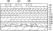
图1显示根据本发明第一实施方案的有机EL显示装置1的结构。有机EL显示装置1用在例如有机EL电视机等中,其中,例如,后面将要说明的多个红色有机EL元件10R、绿色有机EL元件10G和蓝色有机EL元件10B以矩阵形式配置在基板11上的显示区域110中。在显示区域110的周边,设置有作为画面显示的驱动器的信号线驱动电路120和扫描线驱动电路130。FIG. 1 shows the structure of an organic EL display device 1 according to a first embodiment of the present invention. The organic EL display device 1 is used in, for example, an organic EL television or the like, in which, for example, a plurality of red
在显示区域110中设置有像素驱动电路140。图2显示像素驱动电路140的一个例子。像素驱动电路140是形成在后面将要说明的下电极12下层中的有源型驱动电路。具体而言,像素驱动电路140包括驱动晶体管Tr1、写入晶体管Tr2、位于这些晶体管Tr1和Tr2之间的电容器(保持电容)Cs以及位于第一电源线(Vcc)和第二电源线(GND)之间并串联连接至驱动晶体管Tr1的红色有机EL元件10R(或绿色有机EL元件10G、蓝色有机EL元件10B)。驱动晶体管Tr1和写入晶体管Tr2均由普通的薄膜晶体管(TFT)构成,它们的结构例如都可以是反交错结构(被称作底栅型)或者可以是交错结构(顶栅型),没有特殊限制。A
在像素驱动电路140中,多根信号线120A沿列方向布置,多根扫描线130A沿行方向布置。各信号线120A与各扫描线130A之间的交叉点对应于红色有机EL元件10R、绿色有机EL元件10G和蓝色有机EL元件10B中的一个(子像素)。各信号线120A连接至信号线驱动电路120,并从信号线驱动电路120通过信号线120A将图像信号供给到写入晶体管Tr2的源极。各扫描线130A连接至扫描线驱动电路130,并从扫描线驱动电路130通过扫描线130A将扫描信号顺次供给到写入晶体管Tr2的栅极。In the
此外,在显示区域110中,如上所述,整体以矩阵形式顺次布置发红色光的红色有机EL元件10R、发绿色光的绿色有机EL元件10G和发蓝色光的蓝色有机EL元件10B。应指出,彼此相邻的红色有机EL元件10R、绿色有机EL元件10G和蓝色有机EL元件10B的组合构成一个像素。这里,发红色光的红色有机EL元件10R和发绿色光的绿色有机EL元件10G基于来自产生黄色的发光层的光通过滤色器18(红色滤色器和绿色滤色器)而分别呈现出红色和绿色的发光色。Further, in the
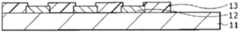
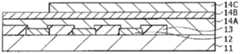
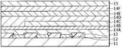
图3显示图1所示的显示区域110的剖面结构。红色有机EL元件10R、绿色有机EL元件10G和蓝色有机EL元件10B均具有以下结构:其中从基板11侧顺次层叠作为阳极的下电极12(第一电极)、隔壁13、包括后面将要说明的发光层(黄色发光层14C和蓝色发光层14D)的有机层14和作为阴极的上电极15(第二电极),其中上述像素驱动电路140的驱动晶体管Tr1和平坦化绝缘膜(未图示)夹在其间。FIG. 3 shows a cross-sectional structure of the
红色有机EL元件10R、绿色有机EL元件10G和蓝色有机EL元件10B均覆盖有保护层16。此外,通过在保护层16的整个表面上利用其间的例如由热固性树脂或紫外线固化性树脂制成的粘合层(未图示)贴合由例如玻璃制成的密封基板17。由此,对各有机EL元件进行密封。Each of the red
基板11是支撑体,其中在它的一个主表面侧上排列形成有红色有机EL元件10R、绿色有机EL元件10G和蓝色有机EL元件10B。公知的成分可以用作基板11。例如,使用石英、玻璃、金属箔或树指的膜或片。在这些材料中,石英或玻璃是优选的。在使用由树脂制成的部件的情况下,其材料的例子包括诸如聚甲基丙烯酸甲酯(PMMA)等甲基丙烯酸树脂类、诸如聚对苯二甲酸乙二醇酯(PET)、聚萘二甲酸乙二醇酯(PEN)或聚萘二甲酸丁二醇酯(PBN)等聚酯类以及聚碳酸酯树脂等。然而,在这种情况下,应该形成层叠结构和进行表面处理,以降低透水性和透气性。The
下电极12在基板11上对应于红色有机EL元件10R、绿色有机EL元件10G和蓝色有机EL元件10B形成。下电极12在层叠方向上的厚度(下面简称为“厚度”)例如为10~1000nm。其材料的例子包括诸如钼(Mo)、铬(Cr)、金(Au)、铂(Pt)、镍(Ni)、铜(Cu)、钨(W)和银(Ag)等金属元素的单质或其合金。或者,下电极12可以具有由这些金属元素中任一种的单质或其合金制成的金属膜以及铟锡氧化物(ITO)、铟锌氧化物(InZnO)或氧化锌(ZnO)与铝(Al)的合金等制成的透明导电膜构成的层叠结构。应指出,当将下电极12用作阳极时,下电极12优选由具有高的空穴注入性的材料制成。然而,即使伴随有由于表面氧化膜的存在以及功函数小造成的空穴注入势垒问题的铝(Al)合金等材料,通过设置适当的空穴注入层14A,也可以用作下电极12的材料。The
隔壁13被设置以确保下电极12与上电极15之间的绝缘性,并使发光区域成为期望形状。隔壁13的材料的例子包括诸如SiO2等无机绝缘材料以及诸如正型感光性的聚苯并噁唑或正型感光性的聚酰亚胺等感光性树脂。隔壁13中设有对应于发光区域的开口。应指出,有机层14和上电极15不仅可以形成在开口上,而且可以形成在隔壁13上。然而,发光仅在隔壁13的开口中产生。此外,尽管在本实施方案中,隔壁13采用由一种材料形成的单层结构,但是隔壁13可以具有由多种材料构成的层叠结构。或者,仅有下电极12被图案化,未设置隔壁13,并且空穴注入层14A和后续的有机层14被设置作为共用层。The
有机EL元件10R、10G和10B中的有机层14例如具有以下结构:从下电极12侧顺次层叠空穴注入层14A、空穴输送层14B、黄色发光层14C、蓝色发光层14D、电子输送层14E和电子注入层14F。在有机层14的这些层中,除了黄色发光层14C之外的各层,即,层14A、14B和14D~14F,被设置作为有机EL元件10R、10G和10B的共用层。黄色发光层14C未设置在蓝色有机EL元件10B上,而是设置在红色有机EL元件10R和绿色有机EL元件10G上。The
空穴注入层14A是用于提高向黄色发光层14C和蓝色发光层14D的空穴注入效率并防止漏光的缓冲层。空穴注入层14A的厚度例如优选为5~100nm,更优选8~50nm。The
可以根据与电极及邻接层的材料的关系适当地选择构成空穴注入层14A的材料。其材料的例子包括聚苯胺、聚噻吩、聚吡咯、聚苯乙炔、聚噻吩乙炔、聚喹啉、聚喹喔啉和其衍生物、在主链或支链中含有芳香族胺结构的聚合物等导电性高分子、金属酞菁(如铜酞菁)和碳。The material constituting the
当用于形成空穴注入层14A的材料是高分子材料时,高分子材料的重均分子量(Mw)可以为5,000~300,000,特别优选约10,000~200,000。或者,可以使用Mw为约2,000~5,000的低聚物。然而,如果Mw小于5,000,则在形成空穴输送层和后续层时空穴注入层可能会发生溶解。如果Mw超过300,000时,则材料可能会凝胶化,从而导致成膜困难。When the material used to form the
用作构成空穴注入层14A的材料的典型导电性高分子的例子包括聚苯胺、低聚苯胺和诸如聚(3,4-亚乙基二氧基噻吩)(PEDOT)等聚二氧噻吩。其他例子包括以H.C.Starck Ltd.制造的Nafion(商标)市售的聚合物或以商品名Liquion(商标)市售的溶液形式的聚合物、Nissan Chemical Industries,Ltd.制造的ELsource(商标)以及Soken Chemical & Engineering Co.,Ltd.制造的导电性高分子Berazol(商标)。Examples of typical conductive polymers used as a material constituting the
红色有机EL元件10R、绿色有机EL元件10G和蓝色有机EL元件10B中的空穴输送层14B用于提高向黄色发光层14C和蓝色发光层14D的空穴输送效率。取决于元件的整体结构,空穴输送层14B的厚度例如优选为10~200nm,更优选15~150nm。The
作为构成空穴输送层14B的高分子材料,可以使用在有机溶剂中溶解的材料。材料的例子包括聚乙烯基咔唑、聚芴、聚苯胺、聚硅烷及其衍生物、在主链或侧链中具有芳香族胺的聚硅氧烷衍生物、聚噻吩和其衍生物及聚吡咯。As the polymer material constituting the
更优选材料的例子包括确保空穴输送层14B对下侧的空穴注入层14A和上侧的黄色发光层14C的良好粘合性、在有机溶剂中可溶解的、并由下式(1)代表的高分子材料:Examples of more preferable materials include those that ensure good adhesion of the

其中A1~A4每一个是1~10个芳香族烃基或其衍生物彼此连接在一起形成的基团或者1~15个杂环基或其衍生物彼此连接在一起形成的基团;n和m每一个是0~10,000的整数,并且n+m是10~20,000的整数。Each of A1 to A4 is a group formed by connecting 1 to 10 aromatic hydrocarbon groups or derivatives thereof or a group formed by connecting 1 to 15 heterocyclic groups or derivatives thereof; n and m Each is an integer of 0 to 10,000, and n+m is an integer of 10 to 20,000.
此外,n部和m部的排列顺序是任意的,并且式(1)的材料可以是无规聚合物、交替共聚物、周期共聚物或嵌段共聚物。此外,n和m每一个优选是5~5,000的整数,更优选10~3,000的整数。此外,n+m优选是10~10,000的整数,更优选20~6,000的整数。In addition, the arrangement order of the n part and the m part is arbitrary, and the material of formula (1) may be a random polymer, an alternating copolymer, a periodic copolymer or a block copolymer. In addition, each of n and m is preferably an integer of 5 to 5,000, more preferably an integer of 10 to 3,000. In addition, n+m is preferably an integer of 10 to 10,000, more preferably an integer of 20 to 6,000.
此外,在式(1)代表的化合物中,A1~A4代表的芳香族烃基的具体例子包括苯、芴、萘、蒽或其衍生物;苯乙炔衍生物;和苯乙烯基衍生物。杂环基的具体例子包括噻吩、吡啶、吡咯、咔唑或其衍生物。Further, in the compound represented by formula (1), specific examples of the aromatic hydrocarbon groups represented by A1 to A4 include benzene, fluorene, naphthalene, anthracene or derivatives thereof; phenylacetylene derivatives; and styryl derivatives. Specific examples of the heterocyclic group include thiophene, pyridine, pyrrole, carbazole or derivatives thereof.
在式(1)代表的化合物中的A1~A4具有取代基的情况下,该取代基例如是碳数1~12的直链或支链烷基或烯基。具体而言,该取代基的优选例子包括甲基、乙基、丙基、异丙基、丁基、异丁基、仲丁基、叔丁基、戊基、己基、庚基、辛基、壬基、癸基、十一烷基、十二烷基、乙烯基和烯丙基。When A1 to A4 in the compound represented by formula (1) have a substituent, the substituent is, for example, a straight-chain or branched alkyl or alkenyl group having 1 to 12 carbons. Specifically, preferred examples of the substituent include methyl, ethyl, propyl, isopropyl, butyl, isobutyl, sec-butyl, tert-butyl, pentyl, hexyl, heptyl, octyl, Nonyl, Decyl, Undecyl, Dodecyl, Vinyl and Allyl.
作为式(1)代表的化合物的具体例子,例如,下式(1-1)~(1-3)代表的化合物是优选的。具体而言,它们是As specific examples of the compound represented by formula (1), for example, compounds represented by the following formulas (1-1) to (1-3) are preferable. Specifically, they are
聚[(9,9-二辛基芴-2,7-二基)-共-(4,4’-(N-(4-仲丁基苯基))二苯基胺)](TFB,式(1-1));Poly[(9,9-dioctylfluorene-2,7-diyl)-co-(4,4'-(N-(4-sec-butylphenyl))diphenylamine)] (TFB, formula (1-1));
聚[(9,9-二辛基芴-2,7-二基)-交替共-(N,N’-双{4-丁基苯基}-联苯胺N,N’-{1,4-二亚苯基})](式(1-2));和Poly[(9,9-dioctylfluorene-2,7-diyl)-alternating co-(N,N'-bis{4-butylphenyl}-benzidine N,N'-{1,4 -diphenylene})] (formula (1-2)); and
聚[(9,9-二辛基芴-2,7-二基)](PFO,式(1-3))。然而,式(1)代表的化合物不限于此。Poly[(9,9-dioctylfluorene-2,7-diyl)] (PFO, formula (1-3)). However, the compound represented by formula (1) is not limited thereto.

当通过电阻加热代表的蒸发法形成空穴注入层14A和空穴输送层14B时,优选的是使用例如以下材料中的任一种:α-萘基苯基苯二胺、卟啉、金属四苯基卟啉、金属萘酞菁、六氰基氮杂苯并菲、7,7,8,8-四氰基对苯醌二甲烷(TCNQ)、7,7,8,8-四氰基-2,3,5,6-四氟对苯醌二甲烷(F4-TCNQ)、四氰基-4,4,4-三(3-甲基苯基苯基氨基)三苯胺、N,N,N’,N’-四(对甲苯基)对苯二胺、N,N,N’,N’-四苯基-4,4’-二氨基联苯、N-苯基咔唑、4-二-对甲苯基氨基二苯乙烯、聚(对苯乙炔)、聚(噻吩乙炔)和聚(2,2’-噻吩基吡咯)。然而,材料不限于此。When the
在黄色发光层14C中,通过施加电场,使电子和空穴彼此再结合,从而发光。取决于元件的整体结构,黄色发光层14C的厚度例如优选为10~200nm,更优选15~100nm。黄色发光层14C由至少一种在500nm~750nm的任意范围内具有至少一个峰值波长的发光材料构成。In the yellow
通过后面将要详细说明的诸如喷墨法等涂布法形成黄色发光层14C。在这种情况下,使用至少一种例如以下的有机溶剂溶解高分子材料和低分子材料,形成混合溶液:甲苯、二甲苯、苯甲醚、环己酮、均三甲苯(1,3,5-三甲基苯)、偏三甲苯(1,2,4-三甲基苯)、二氢苯并呋喃、1,2,3,4-四甲基苯、萘满、环己基苯、1-甲基萘、对甲氧基苯甲醇、二甲基萘、3-甲基联苯、4-甲基联苯、3-异丙基联苯和单异丙基萘。使用该混合溶液形成黄色发光层14C。The yellow
构成黄色发光层14C的发光材料的例子包括下式(2)~(4)代表的磷光性主体材料和荧光性主体材料。Examples of light emitting materials constituting the yellow
其中Z1是含氮烃基或其衍生物;L1是1~4个二价芳香族环基连接在一起形成的基团或其衍生物,具体而言,1~4个芳香族环连接在一起形成的二价基团或其衍生物;和A5和A6每一个是芳香族烃基或芳香族杂环基或其衍生物,但是A5和A6可以彼此连接形成环状结构。Among them, Z1 is a nitrogen-containing hydrocarbon group or its derivatives; L1 is a group formed by linking 1 to 4 divalent aromatic ring groups or its derivatives, specifically, 1 to 4 aromatic rings linked together to form or a derivative thereof; and each of A5 and A6 is an aromatic hydrocarbon group or an aromatic heterocyclic group or a derivative thereof, but A5 and A6 may be connected to each other to form a ring structure.

其中R1~R3每一个独立地是氢原子、1~3个芳香族环缩合在一起形成的芳香族烃基或其衍生物、具有碳数1~6的烃基的1~3个芳香族环缩合在一起形成的芳香族烃基或其衍生物、或具有碳数6~12的芳香族烃基的1~3个芳香族环缩合在一起形成的芳香族烃基或其衍生物。Wherein R1~R3 are each independently a hydrogen atom, an aromatic hydrocarbon group formed by condensing 1~3 aromatic rings or its derivatives, and 1~3 aromatic rings of a hydrocarbon group with a carbon number of 1~6 are condensed in An aromatic hydrocarbon group or a derivative thereof formed together, or an aromatic hydrocarbon group or a derivative thereof formed by condensing 1 to 3 aromatic rings of an aromatic hydrocarbon group having 6 to 12 carbon atoms.

其中R4~R9每一个是氢原子、卤原子、羟基、碳数20以下的烷基、烯基、具有羰基的基团、具有羰基酯基团的基团、具有烷氧基的基团、具有氰基的基团、具有硝基的基团、其衍生物、碳数30以下的具有甲硅烷基的基团、具有芳基的基团、具有杂环基的基团、具有氨基的基团或其衍生物。Wherein each of R4~R9 is a hydrogen atom, a halogen atom, a hydroxyl group, an alkyl group with a carbon number of 20 or less, an alkenyl group, a group with a carbonyl group, a group with a carbonyl ester group, a group with an alkoxy group, a group with A group having a cyano group, a group having a nitro group, a derivative thereof, a group having a silyl group having 30 or less carbon atoms, a group having an aryl group, a group having a heterocyclic group, and a group having an amino group or its derivatives.
式(2)代表的化合物的具体例子包括下式(2-1)~(2-96)代表的化合物。Specific examples of the compound represented by the formula (2) include compounds represented by the following formulas (2-1) to (2-96).


式(3)代表的化合物的具体例子包括下式(3-1)~(3-5)等代表的化合物。Specific examples of the compound represented by the formula (3) include compounds represented by the following formulas (3-1) to (3-5) and the like.

式(4)代表的化合物中R4~R9代表的具有芳基的基团的例子包括苯基、1-萘基、2-萘基、芴基、1-蒽基、2-蒽基、9-蒽基、1-菲基、2-菲基、3-菲基、4-菲基、9-菲基、1-并四苯基、2-并四苯基、9-并四苯基、1-芘基、2-芘基、4-芘基、1-
此外,R4~R9代表的具有杂环基的基团是含有氧原子(O)、氮原子(N)或硫原子(S)作为杂原子的5元或6元芳香族环基,包括碳数2~20的稠合多环芳香族环基。这种杂环基的例子包括噻吩基、呋喃基、吡咯基、吡啶基、喹啉基、喹喔啉基、咪唑并吡啶基和苯并噻唑基。代表性例子包括1-吡咯基、2-吡咯基、3-吡咯基、吡嗪基、2-吡啶基、3-吡啶基、4-吡啶基、1-吲哚基、2-吲哚基、3-吲哚基、4-吲哚基、5-吲哚基、6-吲哚基、7-吲哚基、1-异吲哚基、2-异吲哚基、3-异吲哚基、4-异吲哚基、5-异吲哚基、6-异吲哚基、7-异吲哚基、2-糠偶酰基、3-糠偶酰基、2-苯并呋喃基、3-苯并呋喃基、4-苯并呋喃基、5-苯并呋喃基、6-苯并呋喃基、7-苯并呋喃基、1-异苯并呋喃基、3-异苯并呋喃基、4-异苯并呋喃基、5-异苯并呋喃基、6-异苯并呋喃基、7-异苯并呋喃基、喹啉基、3-喹啉基、4-喹啉基、5-喹啉基、6-喹啉基、7-喹啉基、8-喹啉基、1-异喹啉基、3-异喹啉基、4-异喹啉基、5-异喹啉基、6-异喹啉基、7-异喹啉基、8-异喹啉基、2-喹喔啉基、5-喹喔啉基、6-喹喔啉基、1-咔唑基、2-咔唑基、3-咔唑基、4-咔唑基、9-咔唑基、1-菲啶基、2-菲啶基、3-菲啶基、4-菲啶基、6-菲啶基、7-菲啶基、8-菲啶基、9-菲啶基、10-菲啶基、1-吖啶基、2-吖啶基、3-吖啶基、4-吖啶基和9-吖啶基等。In addition, the group having a heterocyclic group represented by R4~R9 is a 5-membered or 6-membered aromatic ring group containing an oxygen atom (O), a nitrogen atom (N) or a sulfur atom (S) as a heteroatom, including carbon number 2-20 condensed polycyclic aromatic ring groups. Examples of such heterocyclic groups include thienyl, furyl, pyrrolyl, pyridyl, quinolinyl, quinoxalinyl, imidazopyridyl and benzothiazolyl. Representative examples include 1-pyrrolyl, 2-pyrrolyl, 3-pyrrolyl, pyrazinyl, 2-pyridyl, 3-pyridyl, 4-pyridyl, 1-indolyl, 2-indolyl, 3-indolyl, 4-indolyl, 5-indolyl, 6-indolyl, 7-indolyl, 1-isoindolyl, 2-isoindolyl, 3-isoindolyl , 4-isoindolyl, 5-isoindolyl, 6-isoindolyl, 7-isoindolyl, 2-furilyl, 3-furilyl, 2-benzofuryl, 3- Benzofuryl, 4-benzofuryl, 5-benzofuryl, 6-benzofuryl, 7-benzofuryl, 1-isobenzofuryl, 3-isobenzofuryl, 4 -isobenzofuryl, 5-isobenzofuryl, 6-isobenzofuryl, 7-isobenzofuryl, quinolinyl, 3-quinolyl, 4-quinolyl, 5-quinolinyl Linyl, 6-quinolinyl, 7-quinolinyl, 8-quinolinyl, 1-isoquinolinyl, 3-isoquinolinyl, 4-isoquinolinyl, 5-isoquinolinyl, 6 -isoquinolinyl, 7-isoquinolinyl, 8-isoquinolinyl, 2-quinoxalinyl, 5-quinoxalinyl, 6-quinoxalinyl, 1-carbazolyl, 2-carbazolyl Azolyl, 3-carbazolyl, 4-carbazolyl, 9-carbazolyl, 1-phenanthridinyl, 2-phenanthridinyl, 3-phenanthridinyl, 4-phenanthridyl, 6-phenanthridinyl , 7-phenanthridinyl, 8-phenanthridinyl, 9-phenanthridinyl, 10-phenanthridinyl, 1-acridinyl, 2-acridinyl, 3-acridinyl, 4-acridinyl and 9 -Acridinyl etc.
R4~R9代表的具有氨基的基团可以是烷基氨基、芳基氨基和芳烷基氨基等中的任一种。这些基团优选具有碳数1~6的脂肪族烃基和/或1~4个芳香族环基。这种基团的例子包括二甲基氨基、二乙基氨基、二丁基氨基、二苯基氨基、二甲苯基氨基、二联苯基氨基和二萘基氨基。应指出,上述取代基可以形成由两个以上取代基构成的稠合环,或者可以是其衍生物。The amino groups represented by R4 to R9 may be any of alkylamino, arylamino, aralkylamino, and the like. These groups preferably have an aliphatic hydrocarbon group having 1 to 6 carbon atoms and/or 1 to 4 aromatic ring groups. Examples of such groups include dimethylamino, diethylamino, dibutylamino, diphenylamino, xylylamino, biphenylylamino and dinaphthylamino. It should be noted that the above substituents may form a condensed ring composed of two or more substituents, or may be derivatives thereof.
式(4)代表的化合物的具体例子包括下式(4-1)~(4-51)等代表的化合物。Specific examples of the compound represented by the formula (4) include compounds represented by the following formulas (4-1) to (4-51) and the like.


此外,优选的是使用磷光性金属配合物作为掺杂剂。具体而言,优选的是,中心金属是选自元素周期表第7~11族的金属。金属的例子包括铍(Be)、硼(B)、锌(Zn)、镉(Cd)、镁(Mg)、金(Au)、银(Ag)、钯(Pd)、铂(Pt)、铝(Al)、钆(Ga)、钇(Y)、钪(Sc)、钌(Ru)、铑(Rh)、锇(Os)和铱(Ir)。掺杂剂的更具体例子包括下式(5-1)~(5-29)代表的化合物。然而,掺杂剂不限于此。应指出,上述掺杂剂可以单独使用或者两种以上组合使用。此外,可以组合使用中心金属彼此不同的掺杂剂。Furthermore, it is preferred to use phosphorescent metal complexes as dopants. Specifically, it is preferable that the central metal is a metal selected from Groups 7 to 11 of the periodic table. Examples of metals include beryllium (Be), boron (B), zinc (Zn), cadmium (Cd), magnesium (Mg), gold (Au), silver (Ag), palladium (Pd), platinum (Pt), aluminum (Al), gadolinium (Ga), yttrium (Y), scandium (Sc), ruthenium (Ru), rhodium (Rh), osmium (Os), and iridium (Ir). More specific examples of dopants include compounds represented by the following formulas (5-1) to (5-29). However, the dopant is not limited thereto. It should be noted that the above-mentioned dopants may be used alone or in combination of two or more. In addition, dopants whose central metals are different from each other may be used in combination.


此外,除了上述低分子材料之外,尤其是作为黄色发光材料,可以提到的有经三重态发出磷光的双(2-2’-苯并噻吩基)-吡啶-N,C3)(乙酰丙酮)合铱(式(6-1),下面简写为btp2Ir(acac))和双(8-羟基喹啉)锌(式(6-2))。此外,还可以使用将黄色发光材料加到作为代表性绿色发光材料的三(2-苯基吡啶)铱(式(6-3),下面简写为Ir(ppy)3)中以合成黄色光的发光方法。然而,材料和方法不限于此。Furthermore, in addition to the above-mentioned low-molecular materials, bis(2-2'-benzothienyl)-pyridine-N,C3) (acetylacetone ) iridium (formula (6-1), hereinafter abbreviated as btp2Ir(acac)) and bis(8-hydroxyquinoline) zinc (formula (6-2)). In addition, it is also possible to use a method in which a yellow light-emitting material is added to tris(2-phenylpyridine)iridium (formula (6-3), hereinafter abbreviated as Ir(ppy)3) as a representative green light-emitting material to synthesize yellow light. Luminous method. However, materials and methods are not limited thereto.

应指出,构成黄色发光层14C的材料不限于上述式(2-1)~(2-96)、式(3-1)~(3-5)、式(4-1)~(4-51)、式(5-1)~(5-29)和式(6-1)~(6-3)代表的磷光性和荧光性低分子材料。例如,黄色发光层14C可以由通过用磷光发光性低分子材料掺杂高分子材料得到的混合材料构成。除此之外,可以使用例如通过混合下式(7)所示的聚乙烯基咔唑(n是10~5000的整数)和式(6-1)~(6-3)所示的磷光性低分子材料获得的材料。此外,可以通过使用含有磷光发光性的发光单元的磷光发光性高分子材料形成黄色发光层14C。材料的具体例子包括发光性高分子材料,如聚芴系高分子衍生物、聚苯乙炔衍生物、聚苯撑衍生物、聚乙烯基咔唑衍生物和聚噻吩衍生物。应指出,用于黄色发光层14C的高分子材料不仅限于共轭系聚合物,而且还包括悬挂形的非共轭系聚合物及染料混合型的非共轭系聚合物。因此,高分子材料还可以是近年来被研发的树枝状聚合物型高分子发光材料,它由被称作核心的中心分子和配置成覆盖中心并被称为树枝化基元的侧链构成。此外,关于发光部,已知的有从单重态激子发光的发光部、从三重态激子发光的发光部、或者从单重态激子和三重态激子均发光的发光部。在本实施方案的黄色发光层14C中,优选使用从三重态激子发光的发光部。It should be noted that the materials constituting the yellow

形成黄色发光层14C的方法不限于涂布法,可以使用蒸发法或例如激光转写法等代表的热转写法来形成。在通过蒸发法或热转写法形成时,在作为黄色发光层14C的材料的式(2-1)~(2-96)、式(3-1)~(3-5)、式(4-1)~(4-51)、式(5-1)~(5-29)和式(6-1)~(6-3)代表的磷光性和荧光性低分子材料中,优选的是选择并使用例如分子量2000以下的材料。在分子量至少2000的低分子材料的情况下,由于在蒸发和转写时需要高能量的加热,因此材料可能会变性。具体而言,例如,形成在对应于黄色发光层14C的区域中具有开口部的条纹状掩模,然后通过蒸发法沉积黄色发光层14C。在使用热转写法形成的情况下,可以使用现有技术中的热转写法。具体而言,例如,将其上形成转写材料层的转写用基板以及其上预先形成黄色发光层14C和蓝色有机EL元件10B的空穴输送层14B的转写目标基板对向配置,然后进行光照射。由此,对应于转写图案形成黄色发光层14C。The method of forming the yellow light-emitting
在蓝色发光层14D中,通过施加电场,电子和空穴彼此再结合,从而发光。取决于元件的整体结构,蓝色发光层14D的厚度例如优选为2nm~50nm,更优选5nm~30nm。In the blue
蓝色发光层14D由低分子材料形成,并且由至少两种材料构成,即,主体材料和客体材料。主体材料的具体例子包括上式(4-1)~(4-51)代表的化合物。The blue
作为客体材料,使用具有高发光效率的材料。材料的例子包括诸如低分子荧光材料、磷光染料和金属配合物等有机发光材料。更具体而言,该材料是峰值波长在约400~490nm范围内的那些化合物。作为这类化合物,使用诸如萘衍生物、蒽衍生物、并四苯衍生物、苯乙烯胺衍生物或双(吖嗪基)亚甲基硼配合物等有机物质。特别地,优选的是,该材料选自氨基萘衍生物、氨基蒽衍生物、氨基
电子输送层14E用于提高向黄色发光层14C和蓝色发光层14D的电子输送效率,并且在蓝色发光层14D的整个表面上作为共用层形成。取决于元件的整体结构,电子输送层14E的厚度例如优选为5~300nm,更优选10~170nm。The
电子输送层14E的材料的例子包括喹啉、苝、菲咯啉、双苯乙烯基化合物、吡嗪、三唑、噁唑、富勒烯、噁二唑、芴酮和其衍生物以及金属配合物。材料的具体例子包括三(8-羟基喹啉)铝(简写为Alq3)、蒽、萘、菲咯啉、芘、苝、丁二烯、香豆素、C60、吖啶、二苯乙烯、1,10-菲咯啉和其衍生物及金属配合物。Examples of materials for the
用于形成电子输送层14E的有机材料不限于一种材料,多种这类有机材料可以混合使用或以层叠形式使用。此外,上述化合物可以用于形成后面将要说明的电子注入层14F。The organic material used to form the
电子注入层14F用于提高电子注入效率,并且在电子输送层14E的整个表面上作为共用层形成。作为电子注入层14F的材料,可以使用例如作为锂(Li)的氧化物的氧化锂(Li2O)、作为铯(Cs)的复合氧化物的碳酸铯(Cs2CO3)及这些氧化物和复合氧化物的混合物。电子注入层14F不限于这些材料。例如,可以使用以下材料的单质:碱土金属,如钙(Ca)和钡(Ba),碱金属,如锂和铯,功函数小的金属,如铟(In)和镁(Mg),和这些金属的氧化物、复合氧化物和氟化物。或者,为了增强稳定性,可以形成并使用这些金属、氧化物、复合氧化物和氟化物的混合物或合金。此外,还可以使用上述作为电子输送层14E的材料的有机材料。The
上电极15的厚度例如为2~15nm,并且由金属导电膜制成。具体而言,其例如由含有Al、Mg、Ca或Na的合金构成。特别地,镁与银的合金(Mg-Ag合金)由于在薄膜中具有导电性和低吸收而是优选的。Mg-Ag合金中的镁与银的比率没有特别限制,但优选的是,Mg∶Ag的膜厚比为20∶1~1∶1。上电极15的材料也可以是铝与锂的合金(A1-Li合金)。The thickness of the
此外,上电极15可以是含有诸如喹啉铝配合物、苯乙烯胺衍生物或酞菁衍生物等有机发光材料的混合层。在这种情况下,上电极15还可以额外地设置诸如MgAg等透光性材料作为第三层。应指出,在有源矩阵驱动方式的情况下,上电极15以固态膜状形成在基板11上,使得其通过有机层14和隔壁13与下电极12绝缘,并且用作红色有机EL元件10R、绿色有机EL元件10G和蓝色有机EL元件10B的共用电极。In addition, the
保护层16的厚度例如为2~3μm,并且可以由绝缘材料或导电材料形成。作为绝缘材料,优选的是无机非晶绝缘材料,具体而言,例如非晶硅(α-Si)、非晶碳化硅(α-SiC)、非晶氮化硅(α-Si1-xNx)或非晶碳(α-C)。由于这些无机非晶绝缘材料不构成晶粒,所以其透水性低。因此,可以获得良好的保护膜。The
密封基板17位于红色有机EL元件10R、绿色有机EL元件10G和蓝色有机EL元件10B的上电极15侧,与粘合层(未图示)一起将红色有机EL元件10R、绿色有机EL元件10G和蓝色有机EL元件10B密封。在通过密封基板向上发光的顶部发光方式的情况下,密封基板17由对于从红色有机EL元件10R、绿色有机EL元件10G和蓝色有机EL元件10B发出的光透明的材料(例如,玻璃)形成。密封基板17设置有例如滤色器18和作为黑矩阵的遮光膜(未图示)。基于这种结构,在红色有机EL元件10R、绿色有机EL元件10G和蓝色有机EL元件10B中产生的光射出。此外,吸收由红色有机EL元件10R、绿色有机EL元件10G和蓝色有机EL元件10B以及这些元件间的配线所反射的外部光。由此,改善对比度。应指出,在通过下电极发光的底部发光方式的情况下,滤色器18相似地形成在密封基板17下方。The sealing
滤色器18包括红色滤色器18R、绿色滤色器18G和蓝色滤色器18B。这些滤色器对应于红色有机EL元件10R、绿色有机EL元件10G和蓝色有机EL元件10B顺次配置。红色滤色器18R、绿色滤色器18G和蓝色滤色器18B例如具有矩形形状并且其间没有间隙地形成。红色滤色器18R、绿色滤色器18G和蓝色滤色器18B均由混合有颜料的树脂制成。通过选择颜料,可以调节这些滤色器,使得在对应于目标红色、绿色或蓝色波长区域的透光率高,在其他波长区域的透光率低。The color filters 18 include a
此外,滤色器18中高透光率的波长范围与从共振器结构MC1射出的目标光的光谱的峰值波长λ一致。结果,在从密封基板17入射的外部光中,只有波长等于射出的目标光的光谱的峰值波长λ的外部光能够通过滤色器18,而其他波长的外部光被防止进入各色的有机EL元件10R、10G和10B。In addition, the wavelength range of high light transmittance in the
尽管在这种结构中,滤色器18包括红色滤色器18R、绿色滤色器18G和蓝色滤色器18B,但是可以直接使用从蓝色发光层14D发光的光,而无需形成蓝色滤色器18B。Although in this structure, the
遮光膜(未图示)例如由混合有黑色着色剂的光学密度至少为1的黑色树脂膜构成或者由利用薄膜干涉的薄膜滤色器构成。由黑色树脂膜构成的遮光膜由于可以低成本地容易地形成,因而是优选的。薄膜滤色器具有以下结构:其中例如层叠至少一层由金属、金属氮化物或金属氧化物构成的薄膜,并且利用薄膜干涉使光衰减。薄膜滤色器的具体例子包括由铬和氧化铬(III)(Cr2O3)层交替层叠形成的薄膜滤色器。The light-shielding film (not shown) is composed of, for example, a black resin film having an optical density of at least 1 mixed with a black colorant, or a thin-film color filter utilizing thin-film interference. A light-shielding film made of a black resin film is preferable because it can be formed easily at low cost. A thin-film color filter has a structure in which, for example, at least one thin film made of metal, metal nitride, or metal oxide is stacked, and light is attenuated using thin-film interference. Specific examples of the thin film color filter include a thin film color filter formed by alternately laminating layers of chromium and chromium (III) oxide (Cr2 O3 ).
有机EL显示装置1例如可以通过以下方式来制造。The organic EL display device 1 can be manufactured, for example, as follows.
图4示出制造有机EL显示装置1的方法的流程图,图5A~5G示出图4所示的制造方法的顺序步骤。首先,在由上述材料制成的基板11上形成包括驱动晶体管Tr1的像素驱动电路140,并且设置例如由感光性树脂制成的平坦化绝缘膜(未图示)。FIG. 4 shows a flowchart of a method of manufacturing the organic EL display device 1 , and FIGS. 5A to 5G show sequential steps of the manufacturing method shown in FIG. 4 . First, the
(形成下电极12的步骤)(Step of forming lower electrode 12)
接下来,在基板11的整个表面上形成例如由ITO制成的透明导电膜,并且使透明导电膜图案化。由此,如图5A所示,形成分别对应于红色有机EL元件10R、绿色有机EL元件10G和蓝色有机EL元件10B的下电极12(步骤S101)。在这种情况下,下电极12通过平坦化绝缘膜(未图示)的接触孔(未图示)与驱动晶体管Tr1的漏极导通。Next, a transparent conductive film made of, for example, ITO is formed on the entire surface of the
(形成隔壁13的步骤)(Step of forming partition wall 13)
接下来,如图5A所示,通过例如化学气相沉积(CVD)法在下电极12和平坦化绝缘膜(未图示)上沉积诸如SiO2等无机绝缘材料,从而形成隔壁13(步骤S102)。Next, as shown in FIG. 5A, an inorganic insulating material such as SiO2 is deposited on the
在形成隔壁13之后,对基板11的形成有下电极12和隔壁13的那侧表面进行氧等离子体处理。由此,去除附着在表面上的诸如有机物等污染物,从而提高润湿性。具体而言,将基板11加热到预定温度,例如约70~80℃,接下来,在大气压力下使用氧气作为反应气体进行等离子体处理(O2等离子体处理)(步骤S103)。After the
(形成空穴注入层14A的步骤)(Step of Forming the
在进行等离子体处理之后,如图5B所示,在由隔壁13包围的区域内,形成由上述材料制成的空穴注入层14A(步骤S104)。通过诸如旋转涂布法、狭缝印刷法或液滴排出法等涂布法形成空穴注入层14A。特别地,在隔壁13所包围的区域中可以选择性地布置空穴注入层14A的形成材料。在这种情况下,优选使用基于作为液滴排出法的喷墨法或喷嘴涂布法或者凹版印刷法、柔性版印刷法等的选择性印刷法。After performing the plasma treatment, as shown in FIG. 5B , in a region surrounded by
具体而言,在下电极12的露出面上布置作为空穴注入层14A的形成材料的聚苯胺或聚噻吩等的溶液或分散液。其后,进行热处理(干燥处理),从而形成空穴注入层14A。Specifically, a solution or dispersion of polyaniline, polythiophene, or the like, which is a forming material of the
在热处理中,溶剂或分散介质被干燥去除,然后在高温下进行加热。在使用聚苯胺或聚噻吩等的导电性高分子的情况下,大气气氛或氧气气氛是优选的。其原因是由于氧气使导电性高分子氧化而容易表现出导电性。In heat treatment, the solvent or dispersion medium is dried and removed, followed by heating at high temperature. When using a conductive polymer such as polyaniline or polythiophene, an air atmosphere or an oxygen atmosphere is preferable. The reason for this is that oxygen oxidizes the conductive polymer to easily exhibit conductivity.
加热温度优选为150~300℃,更优选180~250℃。取决于温度和气氛,加热时间优选为约5~300分钟,更优选10~240分钟。干燥后的厚度优选为5~100nm,更优选8~50nm。The heating temperature is preferably 150 to 300°C, more preferably 180 to 250°C. Depending on the temperature and atmosphere, the heating time is preferably about 5 to 300 minutes, more preferably 10 to 240 minutes. The thickness after drying is preferably 5 to 100 nm, more preferably 8 to 50 nm.
(形成空穴输送层14B的步骤)(Step of forming
在形成空穴注入层14A之后,如图5C所示,在空穴注入层14A上形成由上述高分子材料制成的空穴输送层14B(步骤S105)。通过诸如旋转涂布法、狭缝印刷法或液滴排出法等涂布法形成空穴输送层14B。特别地,在隔壁13所包围的区域中可以选择性地布置空穴输送层14B的形成材料。在这种情况下,优选使用基于作为液滴排出法的喷墨法或喷嘴涂布法或者凹版印刷法、柔性版印刷法等的选择性印刷法。After the
具体而言,通过例如狭缝印刷法,在空穴注入层14A的露出面上布置作为空穴输送层14B的形成材料的高分子材料和低分子材料的混合溶液或分散液。其后,进行热处理(干燥处理),从而形成空穴输送层14B。Specifically, a mixed solution or dispersion of a high-molecular material and a low-molecular material as a forming material of the
在热处理中,溶剂或分散介质被干燥去除,然后在高温下进行加热。作为涂布气氛和用于干燥和加热溶剂的气氛,优选使用含有氮气(N2)作为主要成分的气氛。氧气和水分的存在可能会使制得的有机EL显示装置的发光效率和寿命降低。特别地,由于在加热步骤中氧气和水分的影响很大,所以此时需要注意。氧气浓度优选为0.1~100ppm,更优选50ppm以下。当氧气存在量大于100ppm时,形成的薄膜的界面可能被污染,因而得到的有机EL显示装置的发光效率和寿命降低。如果氧气浓度小于0.1ppm,尽管元件的特性方面没有问题,但是在现实的大规模生产过程中,用于保持气氛中的氧气浓度小于0.1ppm的设备成本可能要求相当高。In heat treatment, the solvent or dispersion medium is dried and removed, followed by heating at high temperature. As the coating atmosphere and the atmosphere for drying and heating the solvent, an atmosphere containing nitrogen (N2 ) as a main component is preferably used. The presence of oxygen and moisture may reduce the luminous efficiency and lifespan of the organic EL display device produced. In particular, since the influence of oxygen and moisture is large in the heating step, care is required at this time. The oxygen concentration is preferably 0.1 to 100 ppm, more preferably 50 ppm or less. When oxygen is present in an amount greater than 100 ppm, the interface of the formed thin film may be polluted, and thus the luminous efficiency and lifetime of the resulting organic EL display device are reduced. If the oxygen concentration is less than 0.1 ppm, although there is no problem in the characteristics of the element, the equipment cost for maintaining the oxygen concentration in the atmosphere to be less than 0.1 ppm may be required to be considerably high in an actual mass production process.
此外,关于水分,露点例如优选为-80℃~-40℃。此外,露点更优选为-50℃以下,再更优选为-60℃以下。如果水分的露点高于-40℃,则形成的薄膜的界面可能被污染,因而得到的有机EL显示装置的发光效率和寿命降低。如果水分的露点低于-80℃,尽管元件的特性方面没有问题,但是在现实的大规模生产过程中,用于保持气氛的露点低于-80℃的设备成本可能要求相当高。In addition, regarding moisture, the dew point is preferably -80°C to -40°C, for example. In addition, the dew point is more preferably -50°C or lower, even more preferably -60°C or lower. If the dew point of moisture is higher than -40° C., the interface of the formed thin film may be contaminated, and thus the luminous efficiency and lifetime of the obtained organic EL display device may be reduced. If the dew point of the moisture is lower than -80°C, although there is no problem in the characteristics of the element, the equipment cost for keeping the dew point of the atmosphere lower than -80°C may be required to be considerably high in an actual mass production process.
加热温度优选为100~230℃,更优选150~200℃。加热温度优选至少低于在形成空穴注入层14A时的温度。取决于温度和气氛,加热时间优选为约5~300分钟,更优选10~240分钟。取决于元件的整体结构,干燥后的厚度优选为10~200nm,更优选15~150nm。The heating temperature is preferably 100 to 230°C, more preferably 150 to 200°C. The heating temperature is preferably at least lower than the temperature when the
(形成黄色发光层14C的步骤)(Step of forming yellow
在形成空穴输送层14B之后,如图5D所示,形成黄色发光层14C(步骤S106)。作为黄色发光层14C的形成方法,例如使用诸如旋转涂布法和液滴排出法等涂布法。特别地,当在隔壁13所包围的区域中选择性地布置黄色发光层14C的形成材料的情况下,优选使用作为液滴排出法的喷墨法或喷嘴涂布法。具体而言,通过例如喷墨法,在空穴输送层14B的露出面上布置混合溶液或分散液,所述混合溶液或分散液通过将作为黄色发光层14C形成材料的掺杂有1wt%磷光性掺杂剂的磷光性主体材料溶解在二甲苯和环己基苯的2∶8比例的混合溶剂中而得到。其后,按照与上述空穴输送层14B的形成步骤中说明的热处理(干燥处理)相似的方法和条件,进行热处理,从而形成黄色发光层14C。可以通过使用作为有版印刷法的凹版印刷法、柔性版印刷法等选择性印刷法来形成黄色发光层14C。After forming the
可以通过蒸发法形成黄色发光层14C。在这种情况下,将基板移到真空蒸发设备中,然后以例如0.1~
(形成蓝色发光层14D、电子输送层14E、电子注入层14F和上电极15的步骤)(Step of forming blue
在形成黄色发光层14C之后,如图5E所示,通过蒸发法在空穴输送层14B和黄色发光层14C的整个表面上形成由上述材料制成的蓝色发光层14D(步骤S107)。随后,如图5F所示,通过蒸发法在蓝色发光层14D的整个表面上形成电子输送层14E、电子注入层14F和上电极15(步骤S108、S109和S110)。After forming the yellow
在形成上电极15之后,如图5G所示,形成保护层16、密封基板17和滤色器18。具体而言,首先,通过成膜粒子的能量小到对下层没有影响程度的成膜法(例如,蒸发法或CVD法)形成保护层16。例如,当形成由非晶氮化硅制成的保护层16时,通过CVD法形成膜厚2~3μm的保护层16。在这种情况下,为了防止由于有机层14的劣化而导致亮度降低,优选将成膜温度设定为常温。此外,为了防止保护层16的剥落,优选在使膜的应力最小的条件下形成膜。After forming the
在不使用任何掩模的情况下在整个表面上形成作为固态膜的蓝色发光层14D、电子输送层14E、电子注入层14F、上电极15和保护层16。此外,蓝色发光层14D、电子输送层14E、电子注入层14F、上电极15和保护层16优选在未暴露于大气中的情况下在同一成膜装置内连续形成。这样可防止大气中的水分所引起的有机层14的劣化。The blue
应指出,在与下电极12同一步骤中形成辅助电极(未图示)的情况下,在形成上电极15之前,可以通过诸如激光烧蚀等方法去除在辅助电极的上部作为固态膜形成的有机层14。这样允许上电极15直接接触辅助电极,从而改善了接触性。It should be noted that, in the case where an auxiliary electrode (not shown) is formed in the same step as the
在形成保护层16之后,例如,在由上述材料制成的密封基板17上形成由上述材料制成的遮光膜。接下来,通过旋转涂布法等将红色滤色器18R的材料涂布在密封基板17上,然后通过光刻技术使涂布的材料图案化,然后烧结。由此,形成红色滤色器18R。接下来,以与红色滤色器18R相似的方式,顺次形成绿色滤色器18G和蓝色滤色器18B。After the
其后,在保护层16上形成粘合层(未图示),并且通过其间的粘合层将密封基板17贴合到保护层16。通过上述步骤,完成了图1~3所示的有机EL显示装置1。Thereafter, an adhesive layer (not shown) is formed on the
在有机EL显示装置1中,通过写入晶体管Tr2的栅极将扫描信号从扫描线驱动电路130供给到各像素,而通过写入晶体管Tr2从信号线驱动电路120供给的图像信号被保持在保持电容Cs中。即,响应于保持电容Cs中所保持的信号,对驱动晶体管Tr1的开/关进行控制。由此,将驱动电流Id注入到红色有机EL元件10R、绿色有机EL元件10G和蓝色有机EL元件10B,从而通过空穴和电子的再结合进行发光。在下面发光(底部发光)的情况下,光穿过下电极12和基板11射出。在上面发光(顶部发光)的情况下,光穿过上电极15、滤色器18和密封基板17射出。In the organic EL display device 1, a scanning signal is supplied to each pixel from the scanning
在现有技术的有机EL显示装置中,如上所述,基于使用白色光的滤色器方式、三色独立(或四色独立)发光方式等实现全色显示。然而,滤色器方式的问题在于,由于光经由滤色器输出,因此光利用效率降低,并且能耗增加。此外,在具有通过层叠具有发光层的多个有机层而得到并且合成白色光的堆叠结构(级联结构)的有机EL显示装置中,发光效率增强,并且必要的电流减小。然而,级联结构的问题在于,由于多个有机层经由其间的电荷产生层层叠在一起,因此驱动电压增大,并且难于充分减小能耗。此外,如上所述,由于在显示装置中具有高出现频率的颜色是白色和接近黑体辐射线的部分,因此使用白色光是有用的。然而,实际上,红色发光元件、绿色发光元件和蓝色发光元件需要针对色度点调节而被驱动。因此,存在的问题在于,能耗进一步增大。In conventional organic EL display devices, as described above, full-color display is realized based on a color filter method using white light, a three-color independent (or four-color independent) light emission method, and the like. However, the color filter method has problems in that since light is output through the color filter, light utilization efficiency decreases and power consumption increases. Furthermore, in an organic EL display device having a stacked structure (cascade structure) obtained by laminating a plurality of organic layers having a light emitting layer and synthesizing white light, luminous efficiency is enhanced and necessary current is reduced. However, the cascade structure has problems in that since a plurality of organic layers are laminated via charge generation layers in between, driving voltage increases and it is difficult to sufficiently reduce power consumption. In addition, as described above, since the color with a high frequency of occurrence in the display device is white and a portion close to a black-body radiation line, it is useful to use white light. However, actually, the red light emitting element, the green light emitting element and the blue light emitting element need to be driven for chromaticity point adjustment. Therefore, there is a problem in that the energy consumption further increases.
三色独立(或四色独立)发光方式的问题在于,色再现性和发光效率处于权衡关系。作为针对该问题的措施,已经报道了使用产生高视感度和高发光效率的黄色来同时保持色域和发光效率的方法。然而,在三色独立发光方式中,至少各色的发光层需要彼此单独地布置在不同区域中,因此步骤数量比滤色器方式更多。此外,在增加黄色发光层来提高色再现性的情况下,步骤数量更一步增多,存在的问题在于,设备成本和材料成本增加,因而使生产性大大降低。The problem with the three-color independent (or four-color independent) lighting method is that color reproducibility and luminous efficiency are in a trade-off relationship. As a measure against this problem, a method of using yellow that produces high visual sensitivity and high luminous efficiency to simultaneously maintain the color gamut and luminous efficiency has been reported. However, in the three-color independent light-emitting method, at least the light-emitting layers of each color need to be arranged in different regions individually from each other, so the number of steps is larger than in the color filter method. Furthermore, in the case of adding a yellow light-emitting layer to improve color reproducibility, the number of steps is further increased, and there is a problem in that equipment cost and material cost are increased, thereby greatly reducing productivity.
相比而言,在本实施方案的有机EL显示装置1中,黄色发光层14C设置在空穴输送层14B的除了蓝色有机EL元件10B的区域之外的区域上,并且通过具有红色、绿色和蓝色的滤色器分割发光色。这样减少了单独布置发光层的步骤。In contrast, in the organic EL display device 1 of the present embodiment, the yellow
如上所述,在本实施方案的有机EL显示装置1中,黄色发光层14C设置在除了蓝色有机EL元件10B的区域之外的空穴输送层14B上,并且蓝色发光层14D设置在空穴输送层14B和黄色发光层14C的整个表面上。此外,通过具有红色、绿色和蓝色的滤色器分割发光色。因此,减少了单独布置发光层的步骤,并且有机EL显示装置的制造步骤简化。即,可以成本抑制和生产性提高地制作能耗降低的有机EL显示装置。As described above, in the organic EL display device 1 of the present embodiment, the yellow
下面说明本发明的第二至第四实施方案。应指出,与上述第一实施方案相同的构成要素被赋予相同的附图标记,并且不再进行说明。Next, the second to fourth embodiments of the present invention will be described. It should be noted that the same constituent elements as those of the first embodiment described above are given the same reference numerals and will not be described again.
(第二实施方案)(second embodiment)
图6显示根据第二实施方案的有机EL显示装置2的显示区域的剖面结构。红色有机EL元件20R、绿色有机EL元件20G和蓝色有机EL元件20B均具有以下结构:其中从基板11侧顺次层叠作为阳极的下电极12(第一电极)、隔壁13、包括后面将要说明的发光层(黄色发光层24C和蓝色发光层24D)的有机层24和作为阴极的上电极15(第二电极),其中上述像素驱动电路140的驱动晶体管Tr1和平坦化绝缘膜(未图示)夹在其间。本实施方案的有机EL显示装置2与上述第一实施方案的不同之处在于,在黄色发光层24C和蓝色发光层24D之间存在连接层24G。FIG. 6 shows a cross-sectional structure of a display region of an organic
连接层24G用于改善空穴输送层24B和蓝色发光层24D之间以及黄色发光层24C和蓝色发光层24D之间的界面,从而增强空穴注入效率,并限定在黄色发光层24C内产生的激子,从而增强发光效率。取决于元件的整体结构,连接层24G的厚度例如优选为2~30nm,更优选5~15nm。The
连接层24G的形成材料的例子包括联苯胺、苯乙烯胺、三苯胺、卟啉、苯并菲、氮杂苯并菲、四氰基对苯醌二甲烷、三唑、咪唑、噁二唑、聚芳基烷、苯二胺、芳胺、噁唑、蒽、芴酮、腙、二苯乙烯和其衍生物。其他例子包括杂环共轭系单体或低聚物(如乙烯基咔唑系化合物、噻吩系化合物或苯胺系化合物)。通过使用这种材料,在空穴输送层24B和蓝色发光层24D之间界面的污染和注入势垒被抑制,从下电极12侧向蓝色发光层24D供给的空穴注入效率增强。具体而言,通过将连接层24G的基态(S0G)和空穴输送层24B的基态(S0B)之间的能差设置为0.4eV以下,可以保持向蓝色发光层24D的空穴注入效率。Examples of the forming material of the
连接层24G的形成材料的具体优选例子包括下式(8)和(9)代表的低分子材料。Specific preferable examples of the forming material of the
其中A7~A9每一个是芳香族烃基、杂环基或其衍生物。Each of A7-A9 is an aromatic hydrocarbon group, a heterocyclic group or a derivative thereof.

其中L2是2~6个二价芳香族环基连接在一起形成的基团或其衍生物,具体而言,2~6个二价芳香族环连接在一起形成的二价基团或其衍生物,和A10~A13是1~10个芳香族烃基或杂环基或它们的衍生物连接在一起形成的基团。Among them, L2 is a group formed by connecting 2 to 6 divalent aromatic ring groups or its derivatives, specifically, a divalent group formed by connecting 2 to 6 divalent aromatic ring groups or its derivatives substances, and A10~A13 are groups formed by linking 1 to 10 aromatic hydrocarbon groups or heterocyclic groups or their derivatives.
式(8)代表的化合物的具体例子包括下式(8-1)~(8-48)的化合物。Specific examples of the compound represented by the formula (8) include compounds of the following formulas (8-1) to (8-48).


此外,在式(8)代表的化合物中,优选的是使用含有具有二苯并呋喃结构的芳基和具有咔唑结构的芳基的胺化合物。这些胺化合物具有大的单重激励能级和三重激励能级,因此可以有效地阻断蓝色发光层24D的电子。因此,发光效率增大并且向空穴输送层24B的电子注入被抑制。因此,寿命特性增强。此外,黄色发光层24C的三重激子被限制在高的三重激励能级,从而提高了发光效率。Furthermore, among the compounds represented by the formula (8), it is preferable to use an amine compound containing an aryl group having a dibenzofuran structure and an aryl group having a carbazole structure. These amine compounds have large singlet excitation levels and triplet excitation levels, and thus can effectively block electrons of the blue
含有具有二苯并呋喃结构的芳基和具有咔唑结构的芳基的胺化合物的具体例子包括下式(8-49)~(8-323)的化合物。Specific examples of the amine compound containing an aryl group having a dibenzofuran structure and an aryl group having a carbazole structure include compounds of the following formulas (8-49) to (8-323).


式(9)代表的化合物的具体例子包括下式(9-1)~(9-45)的化合物。Specific examples of the compound represented by formula (9) include compounds of the following formulas (9-1) to (9-45).


此外,除了式(2-1)~(2-96)代表的磷光性主体材料之外,还可以使用上述式(2)的通式代表的下式(2-97)~(2-166)的化合物。应指出,尽管具有咔唑基团和吲哚基团的化合物例如被举出作为与L1连接的含氮烃基,但是本发明的化合物不限于此。例如,咪唑基团可以用作与L1连接的含氮烃基。In addition, in addition to the phosphorescent host materials represented by the formulas (2-1) to (2-96), the following formulas (2-97) to (2-166) represented by the general formula of the above formula (2) can also be used. compound of. It should be noted that although compounds having a carbazole group and an indole group are, for example, cited as the nitrogen-containing hydrocarbon group attached to L1, the compound of the present invention is not limited thereto. For example, an imidazole group can be used as the nitrogen-containing hydrocarbon group attached to L1.


图7显示制造有机EL显示装置2的方法的流程图。具体而言,可以通过以下方式来制造。FIG. 7 shows a flowchart of a method of manufacturing the organic
(形成连接层24G的步骤)(Step of forming
在形成黄色发光层24C之后,以例如0.1~
在本实施方案的有机EL显示装置2中,通过在空穴输送层24B和蓝色发光层24D之间设置连接层24G,从下电极12侧向蓝色发光层24D供给的空穴注入效率增强。此外,通过在黄色发光层24C和蓝色发光层24D之间设置连接层24G,可以防止在黄色发光层24C由磷光性材料构成时三重态激子向蓝色发光层24D的扩散,从而获得高效率磷光发光。这样除了第一实施方案的有益效果之外还提供了发光效率进一步增强的有益效果。In the organic
(第三实施方案)(third embodiment)
图8显示根据第三实施方案的有机EL显示装置3的结构。图9显示有机EL显示装置3的显示区域的剖面结构。本实施方案的有机EL显示装置3与上述第一实施方案的不同之处在于,黄色发光元件30Y被加到红色有机EL元件30R、绿色有机EL元件30G和蓝色有机EL元件30B,形成4个子像素结构。红色有机EL元件30R、绿色有机EL元件30G、蓝色有机EL元件30B和黄色有机EL元件30Y均具有以下结构:其中从基板11侧顺次层叠作为阳极的下电极12(第一电极)、隔壁13、包括发光层(黄色发光层34C和蓝色发光层34D)的有机层34和作为阴极的上电极15(第二电极),其中上述像素驱动电路140的驱动晶体管Tr1和平坦化绝缘膜(未图示)夹在其间。此外,与上述第一和第二实施方案相似地,保护层16、密封基板17和滤色器38设置在上电极15上。滤色器38包括红色滤色器38R、绿色滤色器38G、蓝色滤色器38B和黄色滤色器38Y。这些滤色器对应于红色有机EL元件30R、绿色有机EL元件30G、蓝色有机EL元件30B和黄色有机EL元件30Y顺次配置。FIG. 8 shows the structure of an organic EL display device 3 according to the third embodiment. FIG. 9 shows a cross-sectional structure of a display region of the organic EL display device 3 . The organic EL display device 3 of this embodiment is different from the above-mentioned first embodiment in that a yellow light-emitting
在本实施方案的有机EL显示装置3中,黄色发光层30Y被加到红色有机EL元件30R、绿色有机EL元件30G和蓝色有机EL元件30B。上述在白色后具有次高出现频率的接近连接蓝色和黄色的黑体辐射线的部分(具体而言,接近肉色的部分)大多数可以由两种颜色(蓝色和黄色)表现。即,除了第一实施方案的有益效果之外,由于不同于上述使用四色(即,红色、绿色、蓝色和白色)的有机EL显示装置,四色的有机EL元件不需要用于表现接近黑体辐射线的部分,因此实现了能耗可以进一步降低的有益效果。此外,由于蓝色和黄色的发光效率高,因此允许能耗更一步降低。即,可以同时实现成本降低和能耗的大幅降低。In the organic EL display device 3 of the present embodiment, a yellow
(第四实施方案)(fourth embodiment)
图10显示根据第四实施方案的有机EL显示装置4的显示区域的剖面结构。在本实施方案的有机EL显示装置4中,红色有机EL元件40R、绿色有机EL元件40G、蓝色有机EL元件40B和黄色发光元件40Y均具有以下结构:其中从基板11侧顺次层叠作为阳极的下电极12(第一电极)、隔壁13、包括发光层(黄色发光层44C和蓝色发光层44D)的有机层44和作为阴极的上电极15(第二电极),其中上述像素驱动电路140的驱动晶体管Tr1和平坦化绝缘膜(未图示)夹在其间。本实施方案的有机EL显示装置4与上述第三实施方案的不同之处在于,在黄色发光层44C和蓝色发光层44D之间存在连接层44G。FIG. 10 shows a cross-sectional structure of a display region of an organic EL display device 4 according to the fourth embodiment. In the organic EL display device 4 of the present embodiment, each of the red organic EL element 40R, the green organic EL element 40G, the blue organic EL element 40B, and the yellow light-emitting element 40Y has a structure in which the anodes are sequentially stacked from the
与第二实施方案中记载的连接层24G相同,本实施方案的连接层44G用于增强向蓝色发光层44D的空穴注入效率。取决于元件的整体结构,连接层44G的厚度例如优选为2~30nm,更优选5~15nm。作为连接层44G的形成材料,可以使用与连接层24G相同的材料。Like the
在本实施方案的有机EL显示装置4中,通过在空穴输送层44B和蓝色发光层44D之间设置连接层44G,从下电极12侧向蓝色发光层44D供给的空穴注入效率增强。此外,通过在黄色发光层44C和蓝色发光层44D之间设置连接层44G,可以防止在黄色发光层44C由磷光性材料构成时三重态激子向蓝色发光层44D的扩散,从而获得高效率磷光发光。这样除了第三实施方案的有益效果之外还提供了发光效率进一步增强的有益效果。In the organic EL display device 4 of the present embodiment, by providing the connection layer 44G between the hole transport layer 44B and the blue light emitting layer 44D, the injection efficiency of holes supplied from the
(模块和应用例)(modules and application examples)
下面将说明上述第一至第四实施方案记载的有机EL显示装置1~4的应用例。根据上述实施方案的有机EL显示装置1~4能够应用于所有领域的电子设备的显示装置,其中以图像或视频的形式显示从外部输入的视频信号或内部产生的视频信号,例如电视机、数码相机、笔记本个人电脑、诸如手机等移动终端设备和摄像机等。Application examples of the organic EL display devices 1 to 4 described in the first to fourth embodiments described above will be described below. The organic EL display devices 1 to 4 according to the above-described embodiments can be applied to display devices of electronic equipment in all fields in which video signals input from the outside or video signals generated inside are displayed in the form of images or videos, such as televisions, digital Cameras, notebook PCs, mobile terminal devices such as mobile phones, video cameras, etc.
(模块)(module)
根据上述实施方案的有机EL显示装置1~4例如作为如图11所示的模块并入到后面将要说明的应用例1~5等中列出的各种电子设备中。该模块具有以下结构:其中例如在基板11的一侧设置从保护层16和密封基板17露出的区域210,在露出区域210中使信号线驱动电路120和扫描线驱动电路130的配线延伸而形成外部连接端子(未图示)。外部连接端子中可以设置用于信号输入/输出的柔性印刷电路(FPC)板220。The organic EL display devices 1 to 4 according to the above-described embodiments are incorporated, for example, as a module as shown in FIG. 11 into various electronic devices listed in Application Examples 1 to 5 and the like to be described later. This module has a structure in which, for example, a
(应用例1)(Application example 1)
图12显示使用上述实施方案的有机EL显示装置1~4的电视机的外观。电视机例如包括由前面板310和滤光玻璃320构成的画面显示屏幕部300。画面显示屏幕部300由上述实施方案的有机EL显示装置1~4构成。FIG. 12 shows the appearance of a television using the organic EL display devices 1 to 4 of the above-described embodiment. The television includes, for example, a screen
(应用例2)(Application example 2)
图13A和图13B显示使用上述实施方案的有机EL显示装置1~4的数码相机的外观。数码相机例如包括闪光用的发光部410、显示部420、菜单开关430和快门按钮440。显示部420由上述实施方案的有机EL显示装置1~4构成。13A and 13B show the appearance of digital cameras using the organic EL display devices 1 to 4 of the above-described embodiments. A digital camera includes, for example, a light emitting unit 410 for flash, a
(应用例3)(Application example 3)
图14显示使用上述实施方案的有机EL显示装置1~4的笔记本个人电脑的外观。笔记本个人电脑例如包括主体510、在输入文字等时操作的键盘520和用于显示图像的显示部530。显示部530由上述实施方案的有机EL显示装置1~4构成。FIG. 14 shows the appearance of a notebook personal computer using the organic EL display devices 1 to 4 of the above-mentioned embodiment. The notebook personal computer includes, for example, a
(应用例4)(Application example 4)
图15显示使用上述实施方案的有机EL显示装置1~4的摄像机的外观。摄像机例如包括主体部610、设于主体部610的前侧表面上的目标拍摄镜头620、拍摄开始/停止开关630和显示部640。显示部640由上述实施方案的有机EL显示装置1~4构成。FIG. 15 shows the appearance of video cameras using the organic EL display devices 1 to 4 of the above-described embodiments. The video camera includes, for example, a
(应用例5)(Application example 5)
图16A~16G显示使用上述实施方案的有机EL显示装置1~4的手机的外观。手机例如包括通过连接部(铰链部)730连接在一起的上壳体710和下壳体720,还包括显示部740、子显示部750、画面灯760和相机770。显示部740或子显示部750由上述实施方案的有机EL显示装置1~4构成。16A to 16G show the appearance of mobile phones using the organic EL display devices 1 to 4 of the above-described embodiments. The mobile phone includes, for example, an
尽管上面参照第一至第四实施方案说明了本发明的技术,但本发明不限于上述实施方案等,可以做出各种变化。Although the technique of the present invention has been described above with reference to the first to fourth embodiments, the present invention is not limited to the above-described embodiments and the like, and various changes can be made.
此外,例如,在上述实施方案中描述的各层的材料、厚度、成膜方法和成膜条件等不受限制。还可以使用其他材料和厚度以及其他成膜方法和成膜条件。In addition, for example, the materials, thicknesses, film-forming methods, film-forming conditions, and the like of the respective layers described in the above-mentioned embodiments are not limited. Other materials and thicknesses as well as other film-forming methods and film-forming conditions can also be used.
此外,尽管在上述实施方案中具体说明了例如有机EL元件10R、10G和10B等的结构,但是不必须包括所有的层,还可以包括其他层。例如,可以省略在空穴注入层14A上形成空穴输送层14B,发光层16C可以通过涂布法直接设置在空穴注入层14A上。In addition, although the structure of, for example, the
此外,尽管在上述实施方案等中,电子输送层14E例如形成为一种材料的单层,但是这种结构不受限制,例如电子输送层14E可以是由两种以上材料形成的混合层或者可以是不同材料层叠置而成的层叠结构。Furthermore, although in the above-described embodiments and the like, the
在上述第二实施方案中,使用具有红色滤色器28R、绿色滤色器28G和蓝色滤色器28B的三色的滤色器18。然而,如第一实施方案中所述的,蓝色发光元件20B的蓝色滤色器28B不需要设置。相似地,在上述第三和第四实施方案中,在红色滤色器38R(48R)、绿色滤色器38G(48G)、蓝色滤色器38B(48B)和黄色滤色器38Y(48Y)中,可以未设置蓝色滤色器38B(48B)和黄色滤色器38Y(48Y),从黄色发光层34C(44C)和蓝色发光层34D(44D)发出的光可以原样使用。In the second embodiment described above, the
此外,对于红色有机EL元件10R(20R,30R,40R)、绿色有机EL元件10G(20G,30G,40G)和蓝色有机EL元件10B(20B,30B,40B)(和黄色有机EL元件30Y,40Y)在基板11上的配置没有特定限制。例如,在上述实施方案中,蓝色、红色、绿色和黄色有机EL元件平行配置。然而,蓝色有机EL元件可以在平行形成的红色、绿色和黄色有机EL元件的下方或上方配置,使其垂直于红色、绿色和黄色有机EL元件的纵向。Furthermore, for the red
此外,尽管在上述实施方案等中,描述了有源矩阵型显示装置的情况,但是本发明的实施方案也适用于无源矩阵型显示装置。此外,有源矩阵驱动的像素驱动电路的结构不限于上述实施方案描述的结构,在需要时还可以加入电容元件和晶体管。在这种情况下,除了上述的信号线驱动电路120和扫描线驱动电路130之外,根据像素驱动电路的变化,可能还加入必要的驱动电路。Furthermore, although in the above-described embodiments and the like, the case of an active matrix type display device has been described, the embodiments of the present invention are also applicable to a passive matrix type display device. In addition, the structure of the pixel driving circuit driven by the active matrix is not limited to the structure described in the above embodiments, and capacitive elements and transistors can also be added if necessary. In this case, in addition to the above-mentioned signal
Claims (14)
Translated fromChineseApplications Claiming Priority (2)
| Application Number | Priority Date | Filing Date | Title |
|---|---|---|---|
| JP2011068246AJP2012204164A (en) | 2011-03-25 | 2011-03-25 | Organic el display device and method for manufacturing the same |
| JP2011-068246 | 2011-03-25 |
Publications (1)
| Publication Number | Publication Date |
|---|---|
| CN102694001Atrue CN102694001A (en) | 2012-09-26 |
Family
ID=46859355
Family Applications (1)
| Application Number | Title | Priority Date | Filing Date |
|---|---|---|---|
| CN2012100637769APendingCN102694001A (en) | 2011-03-25 | 2012-03-12 | Organic electroluminescence display and method of manufacturing the same |
Country Status (5)
| Country | Link |
|---|---|
| US (1) | US20120242218A1 (en) |
| JP (1) | JP2012204164A (en) |
| KR (1) | KR20120109301A (en) |
| CN (1) | CN102694001A (en) |
| TW (1) | TWI566394B (en) |
Cited By (4)
| Publication number | Priority date | Publication date | Assignee | Title |
|---|---|---|---|---|
| CN103915471A (en)* | 2012-12-31 | 2014-07-09 | 乐金显示有限公司 | Organic light emitting diode display device and method for manufacturing the same |
| CN103985731A (en)* | 2013-02-08 | 2014-08-13 | 株式会社日本显示器 | Light-emitting element display device |
| CN104966787A (en)* | 2015-07-17 | 2015-10-07 | 京东方科技集团股份有限公司 | Light emitting diode, display substrate, manufacturing method thereof and display device |
| CN110383162A (en)* | 2017-02-23 | 2019-10-25 | 株式会社理光 | The production method of electrochromic display device and electrochromic display device |
Families Citing this family (16)
| Publication number | Priority date | Publication date | Assignee | Title |
|---|---|---|---|---|
| JP5779051B2 (en)* | 2011-09-08 | 2015-09-16 | 株式会社Joled | Display device, manufacturing method thereof, and electronic device |
| KR102009881B1 (en)* | 2013-03-26 | 2019-08-12 | 엘지디스플레이 주식회사 | Organic light emitting diode display device |
| KR102090717B1 (en)* | 2013-09-24 | 2020-03-19 | 삼성디스플레이 주식회사 | Light emitting panel, control method thereof and display apparatus using the same |
| CN103715367B (en) | 2013-12-24 | 2016-03-30 | 合肥京东方光电科技有限公司 | Organic light emitting diode and electronic equipment |
| JP2014220248A (en)* | 2014-06-25 | 2014-11-20 | 三菱化学株式会社 | Method of manufacturing organic electroluminescent element |
| CN104112766B (en)* | 2014-07-22 | 2017-02-15 | 深圳市华星光电技术有限公司 | Color display device structure |
| CN112992992A (en)* | 2014-10-01 | 2021-06-18 | 索尼公司 | Display device and electronic apparatus |
| KR102362620B1 (en) | 2014-12-09 | 2022-02-14 | 삼성디스플레이 주식회사 | Organic light emitting display and manufacturing method thereof |
| CN104766875B (en) | 2015-03-30 | 2019-12-13 | 昆山工研院新型平板显示技术中心有限公司 | Pixel arrangement method and organic electroluminescence device with shared blue light emitting layer |
| KR102466686B1 (en) | 2015-04-15 | 2022-11-14 | 삼성디스플레이 주식회사 | Light emitting display device |
| KR20170043136A (en)* | 2015-10-12 | 2017-04-21 | 삼성디스플레이 주식회사 | Organic light emitting diode display |
| KR20170133564A (en)* | 2016-05-25 | 2017-12-06 | 삼성디스플레이 주식회사 | Organic light emitting display |
| WO2018181049A1 (en)* | 2017-03-30 | 2018-10-04 | 株式会社クオルテック | Method for manufacturing el display panel, manufacturing device for el display panel, el display panel, and el display device |
| KR102604263B1 (en)* | 2018-07-31 | 2023-11-17 | 엘지디스플레이 주식회사 | Display device |
| JP7415561B2 (en)* | 2020-01-06 | 2024-01-17 | セイコーエプソン株式会社 | Organic electroluminescent devices and electronic equipment |
| JP7419821B2 (en) | 2020-01-06 | 2024-01-23 | セイコーエプソン株式会社 | Organic electroluminescent devices and electronic equipment |
Citations (10)
| Publication number | Priority date | Publication date | Assignee | Title |
|---|---|---|---|---|
| CN1543659A (en)* | 2001-05-16 | 2004-11-03 | ����˹�ٴ�ѧ���»� | High Efficiency Multicolor Electrophosphorescent OLED |
| CN1575065A (en)* | 2003-06-13 | 2005-02-02 | 精工爱普生株式会社 | Organic electroluminescent device, method for driving the same, illumination device, and electronic apparatus |
| WO2006009024A1 (en)* | 2004-07-23 | 2006-01-26 | Konica Minolta Holdings, Inc. | Organic electroluminescent device, display and illuminating device |
| US20060238118A1 (en)* | 2005-04-25 | 2006-10-26 | Eastman Kodak Company | OLED multicolor displays |
| WO2007111192A1 (en)* | 2006-03-24 | 2007-10-04 | Konica Minolta Holdings, Inc. | Organic electroluminescent element, and organic electroluminescent display |
| CN101128559A (en)* | 2004-12-17 | 2008-02-20 | 伊斯曼柯达公司 | Phosphorescent OLEDs with exciton blocking layer |
| CN101213683A (en)* | 2005-06-29 | 2008-07-02 | 伊斯曼柯达公司 | Broadband optical tandem OLED display |
| CN101355140A (en)* | 2007-07-23 | 2009-01-28 | 索尼株式会社 | Organic electroluminescent device and display device |
| CN101714613A (en)* | 2008-09-30 | 2010-05-26 | 乐金显示有限公司 | Organic light emitting diodde desplay device |
| WO2010140549A1 (en)* | 2009-06-03 | 2010-12-09 | コニカミノルタホールディングス株式会社 | Organic electroluminescent element, method for driving same, and illuminating device comprising same |
Family Cites Families (3)
| Publication number | Priority date | Publication date | Assignee | Title |
|---|---|---|---|---|
| US7030553B2 (en)* | 2003-08-19 | 2006-04-18 | Eastman Kodak Company | OLED device having microcavity gamut subpixels and a within gamut subpixel |
| JP4895490B2 (en)* | 2003-09-30 | 2012-03-14 | 三洋電機株式会社 | Organic EL panel |
| US7602119B2 (en)* | 2005-04-25 | 2009-10-13 | Eastman Kodak Company | OLED with magenta and green emissive layers |
- 2011
- 2011-03-25JPJP2011068246Apatent/JP2012204164A/enactivePending
- 2012
- 2012-02-28USUS13/406,769patent/US20120242218A1/ennot_activeAbandoned
- 2012-03-06KRKR1020120022735Apatent/KR20120109301A/ennot_activeCeased
- 2012-03-12CNCN2012100637769Apatent/CN102694001A/enactivePending
- 2012-03-15TWTW101108857Apatent/TWI566394B/ennot_activeIP Right Cessation
Patent Citations (10)
| Publication number | Priority date | Publication date | Assignee | Title |
|---|---|---|---|---|
| CN1543659A (en)* | 2001-05-16 | 2004-11-03 | ����˹�ٴ�ѧ���»� | High Efficiency Multicolor Electrophosphorescent OLED |
| CN1575065A (en)* | 2003-06-13 | 2005-02-02 | 精工爱普生株式会社 | Organic electroluminescent device, method for driving the same, illumination device, and electronic apparatus |
| WO2006009024A1 (en)* | 2004-07-23 | 2006-01-26 | Konica Minolta Holdings, Inc. | Organic electroluminescent device, display and illuminating device |
| CN101128559A (en)* | 2004-12-17 | 2008-02-20 | 伊斯曼柯达公司 | Phosphorescent OLEDs with exciton blocking layer |
| US20060238118A1 (en)* | 2005-04-25 | 2006-10-26 | Eastman Kodak Company | OLED multicolor displays |
| CN101213683A (en)* | 2005-06-29 | 2008-07-02 | 伊斯曼柯达公司 | Broadband optical tandem OLED display |
| WO2007111192A1 (en)* | 2006-03-24 | 2007-10-04 | Konica Minolta Holdings, Inc. | Organic electroluminescent element, and organic electroluminescent display |
| CN101355140A (en)* | 2007-07-23 | 2009-01-28 | 索尼株式会社 | Organic electroluminescent device and display device |
| CN101714613A (en)* | 2008-09-30 | 2010-05-26 | 乐金显示有限公司 | Organic light emitting diodde desplay device |
| WO2010140549A1 (en)* | 2009-06-03 | 2010-12-09 | コニカミノルタホールディングス株式会社 | Organic electroluminescent element, method for driving same, and illuminating device comprising same |
Cited By (7)
| Publication number | Priority date | Publication date | Assignee | Title |
|---|---|---|---|---|
| CN103915471A (en)* | 2012-12-31 | 2014-07-09 | 乐金显示有限公司 | Organic light emitting diode display device and method for manufacturing the same |
| CN103915471B (en)* | 2012-12-31 | 2017-03-01 | 乐金显示有限公司 | Organic LED display device and its manufacture method |
| US10453902B2 (en) | 2012-12-31 | 2019-10-22 | Lg Display Co., Ltd. | Organic light emitting diode display device and method for manufacturing the same |
| CN103985731A (en)* | 2013-02-08 | 2014-08-13 | 株式会社日本显示器 | Light-emitting element display device |
| CN104966787A (en)* | 2015-07-17 | 2015-10-07 | 京东方科技集团股份有限公司 | Light emitting diode, display substrate, manufacturing method thereof and display device |
| CN110383162A (en)* | 2017-02-23 | 2019-10-25 | 株式会社理光 | The production method of electrochromic display device and electrochromic display device |
| US11269229B2 (en) | 2017-02-23 | 2022-03-08 | Ricoh Company, Ltd. | Electrochromic display device and production method of electrochromic display device |
Also Published As
| Publication number | Publication date |
|---|---|
| TWI566394B (en) | 2017-01-11 |
| JP2012204164A (en) | 2012-10-22 |
| US20120242218A1 (en) | 2012-09-27 |
| KR20120109301A (en) | 2012-10-08 |
| TW201301501A (en) | 2013-01-01 |
Similar Documents
| Publication | Publication Date | Title |
|---|---|---|
| CN102655164B (en) | Organic electroluminescence display device and method of manufacturing same and manufacture method thereof | |
| CN102694001A (en) | Organic electroluminescence display and method of manufacturing the same | |
| JP5678487B2 (en) | Organic EL display device | |
| CN102694000B (en) | Organic electroluminescence display device and method of manufacturing same and manufacture method thereof | |
| JP5861169B2 (en) | Organic EL display device and manufacturing method thereof | |
| CN102456711B (en) | Organic electroluminescence display device and method of manufacturing same and manufacture method thereof | |
| JP5515661B2 (en) | Manufacturing method of organic EL display device | |
| JP5819069B2 (en) | Organic EL display device | |
| US9954169B2 (en) | Organic EL display and method of manufacturing the same | |
| CN105265023B (en) | Organic EL display device |
Legal Events
| Date | Code | Title | Description |
|---|---|---|---|
| C06 | Publication | ||
| PB01 | Publication | ||
| SE01 | Entry into force of request for substantive examination | ||
| SE01 | Entry into force of request for substantive examination | ||
| ASS | Succession or assignment of patent right | Owner name:JANPAN ORGANIC RATE DISPLAY CO., LTD. Free format text:FORMER OWNER: SONY CORP Effective date:20150727 | |
| C41 | Transfer of patent application or patent right or utility model | ||
| TA01 | Transfer of patent application right | Effective date of registration:20150727 Address after:Tokyo, Japan Applicant after:The special display of the organic thunder of Japan of Co., Ltd. Address before:Tokyo, Japan Applicant before:Sony Corp | |
| RJ01 | Rejection of invention patent application after publication | ||
| RJ01 | Rejection of invention patent application after publication | Application publication date:20120926 |