CN102683468A - Emitter structure of crystal silicon heterojunction solar battery - Google Patents
Emitter structure of crystal silicon heterojunction solar batteryDownload PDFInfo
- Publication number
- CN102683468A CN102683468ACN2012101828759ACN201210182875ACN102683468ACN 102683468 ACN102683468 ACN 102683468ACN 2012101828759 ACN2012101828759 ACN 2012101828759ACN 201210182875 ACN201210182875 ACN 201210182875ACN 102683468 ACN102683468 ACN 102683468A
- Authority
- CN
- China
- Prior art keywords
- layer
- doped
- emitter
- crystalline silicon
- solar cell
- Prior art date
- Legal status (The legal status is an assumption and is not a legal conclusion. Google has not performed a legal analysis and makes no representation as to the accuracy of the status listed.)
- Pending
Links
- XUIMIQQOPSSXEZ-UHFFFAOYSA-NSiliconChemical compound[Si]XUIMIQQOPSSXEZ-UHFFFAOYSA-N0.000titleabstractdescription6
- 229910052710siliconInorganic materials0.000titleabstractdescription6
- 239000010703siliconSubstances0.000titleabstractdescription6
- 239000013078crystalSubstances0.000titleabstract2
- 229910021419crystalline siliconInorganic materials0.000claimsabstractdescription57
- 229910021417amorphous siliconInorganic materials0.000claimsabstractdescription54
- 239000002131composite materialSubstances0.000claimsabstractdescription4
- 238000006243chemical reactionMethods0.000abstractdescription5
- 230000004888barrier functionEffects0.000abstractdescription2
- 239000010410layerSubstances0.000description76
- 239000010408filmSubstances0.000description14
- 239000002356single layerSubstances0.000description13
- 238000005516engineering processMethods0.000description5
- 238000002360preparation methodMethods0.000description4
- 239000010409thin filmSubstances0.000description4
- 238000004458analytical methodMethods0.000description3
- 238000000034methodMethods0.000description3
- 238000002161passivationMethods0.000description3
- 238000004088simulationMethods0.000description3
- 239000000969carrierSubstances0.000description2
- 238000010586diagramMethods0.000description2
- 238000005215recombinationMethods0.000description2
- 230000006798recombinationEffects0.000description2
- 241000282414Homo sapiensSpecies0.000description1
- 230000015556catabolic processEffects0.000description1
- 230000008094contradictory effectEffects0.000description1
- 230000007547defectEffects0.000description1
- 238000006731degradation reactionMethods0.000description1
- 238000011161developmentMethods0.000description1
- 230000000694effectsEffects0.000description1
- 230000005684electric fieldEffects0.000description1
- 238000005286illuminationMethods0.000description1
- 238000009776industrial productionMethods0.000description1
- 238000010248power generationMethods0.000description1
- 239000002994raw materialSubstances0.000description1
- 238000012827research and developmentMethods0.000description1
Images


Classifications
- Y—GENERAL TAGGING OF NEW TECHNOLOGICAL DEVELOPMENTS; GENERAL TAGGING OF CROSS-SECTIONAL TECHNOLOGIES SPANNING OVER SEVERAL SECTIONS OF THE IPC; TECHNICAL SUBJECTS COVERED BY FORMER USPC CROSS-REFERENCE ART COLLECTIONS [XRACs] AND DIGESTS
- Y02—TECHNOLOGIES OR APPLICATIONS FOR MITIGATION OR ADAPTATION AGAINST CLIMATE CHANGE
- Y02E—REDUCTION OF GREENHOUSE GAS [GHG] EMISSIONS, RELATED TO ENERGY GENERATION, TRANSMISSION OR DISTRIBUTION
- Y02E10/00—Energy generation through renewable energy sources
- Y02E10/50—Photovoltaic [PV] energy
Landscapes
- Photovoltaic Devices (AREA)
Abstract
Translated fromChineseDescription
Translated fromChinese技术领域technical field
本发明涉及太阳电池领域,尤其涉及一种晶硅异质结太阳电池的发射极结构。The invention relates to the field of solar cells, in particular to an emitter structure of a crystalline silicon heterojunction solar cell.
背景技术Background technique
在化石能源等不可再生能源日益枯竭的今天,能源危机日益逼近,新的能源以及可再生能源技术亟待开发应用,太阳能是人类可利用的最重要的可再生清洁能源之一。在太阳能利用技术中,太阳能发电是非常重要且很具潜力的一类,而硅基太阳电池以其丰富的原材料来源及相对成熟的制备技术受到人们的广泛关注,是太阳电池的主流产品类别。现今硅基太阳电池的结构随着技术的发展不断的被改进优化。以晶体硅为基础的a-Si:H/c-Si结构的异质结太阳电池是目前具有大批量产业化生产技术水准的太阳电池中转换效率最高的一类,是目前业内攻关研发的重点之一。针对a-Si:H/c-Si结构的异质结太阳电池,目前关注的焦点在于晶体硅表面钝化层-本征a-Si:H的性能的改进。对于其发射极层-重掺杂的a-Si:H层采用与非晶硅薄膜太阳电池相同的单层p-(或n-)a-Si:H薄膜,厚度通常为10~20nm。发射极为太阳电池pn结结构中非常关键的一部分,其性能的优劣对太阳电池的性能具有决定性的影响。目前所采用的单层p-(或n-)a-Si:H薄膜结构,为满足形成优异内建电场,并且与外界导电层形成良好欧姆接触的要求,必须采用很高的掺杂浓度,一般高于2×1019cm-3。如此高的掺杂浓度会导致薄膜中的缺陷态密度过多,增加的光生载流子的复合概率,又导致太阳电池性能的劣化。这是相互矛盾的现象;这一问题尚未得到解决,现阶段业内也未有很好的解决这一矛盾的方法的报道。Today, when non-renewable energy sources such as fossil energy are increasingly exhausted, the energy crisis is approaching day by day, and new energy and renewable energy technologies need to be developed and applied urgently. Solar energy is one of the most important renewable clean energy available to human beings. In solar energy utilization technology, solar power generation is a very important and promising category, and silicon-based solar cells have attracted widespread attention due to their abundant raw material sources and relatively mature preparation technologies, and are the mainstream product category of solar cells. The structure of today's silicon-based solar cells has been continuously improved and optimized with the development of technology. The heterojunction solar cell with a-Si:H/c-Si structure based on crystalline silicon is the type with the highest conversion efficiency among solar cells with mass industrial production technology level, and is the focus of research and development in the industry. one. For heterojunction solar cells with a-Si:H/c-Si structure, the current focus is on the improvement of the performance of the intrinsic a-Si:H passivation layer on the surface of crystalline silicon. For its emitter layer-heavily doped a-Si:H layer, the same single-layer p-(or n-)a-Si:H film is used as the amorphous silicon thin film solar cell, and the thickness is usually 10~20nm. The emitter is a very critical part of the pn junction structure of the solar cell, and its performance has a decisive impact on the performance of the solar cell. The currently used single-layer p-(or n-) a-Si:H film structure must adopt a very high doping concentration in order to meet the requirements of forming an excellent built-in electric field and forming a good ohmic contact with the external conductive layer. Generally higher than 2×1019 cm-3 . Such a high doping concentration will lead to too much defect state density in the film, increasing the recombination probability of photogenerated carriers, and leading to the degradation of solar cell performance. This is a contradictory phenomenon; this problem has not been resolved, and there is no report on a good solution to this contradiction in the industry at this stage.
发明内容Contents of the invention
本发明的目的在于提供一种晶硅异质结太阳电池的发射极结构,它具有提高开路电压,欧姆接触良好,同时减少载流子的损耗,获得更高转换效率的太阳电池的优点。The object of the present invention is to provide an emitter structure of a crystalline silicon heterojunction solar cell, which has the advantages of increased open circuit voltage, good ohmic contact, reduced carrier loss, and higher conversion efficiency solar cells.
本发明是这样来实现的,一种晶硅异质结太阳电池的发射极结构,其特征在于:它为双层梯度掺杂浓度的非晶硅薄膜(a-Si:H)构成的发射极结构,以重掺杂p-a-Si:H层/浅掺杂p-a-Si:H层或重掺杂n-a-Si:H层/浅掺杂n-a-Si:H层的复合结构作为a-Si:H/c-Si结构的晶硅异质结太阳电池的发射极,其中重掺杂层与导电层连接,浅掺杂层与晶体硅表面的本征a-Si:H层连接,发射极的掺杂类型由晶体硅的掺杂类型决定:晶体硅为n-型晶体硅,则发射极为:重掺杂p-a-Si:H层/浅掺杂p-a-Si:H层结构;晶体硅为p-型晶体硅,则发射极为:重掺杂n-a-Si:H层/浅掺杂n-a-Si:H层;所述的重掺杂p-a-Si:H层或重掺杂n-a-Si:H层的有效掺杂浓度范围为1×1019cm-3~5×1020cm-3,薄膜层的厚度为1~10nm;所述的浅掺杂p-a-Si:H层或浅掺杂n-a-Si:H层的有效掺杂浓度范围为1×1018cm-3~4×1019cm-3,薄膜层的厚度为5~30nm。The present invention is achieved in this way, an emitter structure of a crystalline silicon heterojunction solar cell, which is characterized in that it is an emitter composed of a double-layer gradient doping concentration amorphous silicon film (a-Si:H) Structure, with heavily doped pa-Si:H layer/shallowly doped pa-Si:H layer or heavily doped na-Si:H layer/shallowly doped na-Si:H layer composite structure as a-Si: The emitter of the crystalline silicon heterojunction solar cell with the H/c-Si structure, in which the heavily doped layer is connected to the conductive layer, the shallow doped layer is connected to the intrinsic a-Si:H layer on the surface of the crystalline silicon, and the emitter’s The doping type is determined by the doping type of crystalline silicon: crystalline silicon is n-type crystalline silicon, and the emitter is: heavily doped pa-Si:H layer/shallowly doped pa-Si:H layer structure; crystalline silicon is p -type crystalline silicon, the emitter is: heavily doped na-Si:H layer/shallowly doped na-Si:H layer; the heavily doped pa-Si:H layer or heavily doped na-Si:H The effective doping concentration range of the layer is 1×1019 cm-3 ~5×1020 cm-3 , and the thickness of the film layer is 1~10nm; the lightly doped pa-Si:H layer or lightly doped na - The effective doping concentration range of the Si:H layer is 1×1018 cm-3 ~4×1019 cm-3 , and the thickness of the thin film layer is 5~30nm.
本发明的技术效果是:本发明的双层梯度掺杂的发射极结构,相比于单层发射极结构,具有以下方面的优点:1、浅掺杂层中掺杂浓度低,减少了发射极中的光生载流子的复合,提高太阳电池的光生电流和效率;2、重掺杂层的高掺杂浓度减少了发射极与TCO透明导电层的接触势垒,具有更好的欧姆接触特性,可提高电池的开路电压和填充因子。The technical effect of the present invention is: compared with the single-layer emitter structure, the double-layer gradiently doped emitter structure of the present invention has the following advantages: 1. The doping concentration in the shallowly doped layer is low, reducing the emission The recombination of photogenerated carriers in the pole improves the photogenerated current and efficiency of the solar cell; 2. The high doping concentration of the heavily doped layer reduces the contact barrier between the emitter and the TCO transparent conductive layer, which has better ohmic contact characteristics, can improve the open circuit voltage and fill factor of the battery.
附图说明Description of drawings
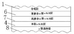
图1为本发明晶硅异质结的双层梯度掺杂发射极的一种结构示意图。FIG. 1 is a schematic diagram of a structure of a double-layer gradiently doped emitter of a crystalline silicon heterojunction according to the present invention.
图2为本发明晶硅异质结的双层梯度掺杂发射极的另一种结构示意图。FIG. 2 is a schematic diagram of another structure of a double-layer gradiently doped emitter of a crystalline silicon heterojunction according to the present invention.
图3为本发明模拟分析所得到的n-型晶体硅片上单层发射极与双层梯度掺Fig. 3 is the single-layer emitter and the double-layer gradient doping on the n-type crystalline silicon wafer obtained by the simulation analysis of the present invention.
杂发射极的晶硅异质结太阳电池的AM1.5G光照条件下的IV曲线对比。Comparison of IV curves of crystalline silicon heterojunction solar cells with heteroemitters under AM1.5G light conditions.
图4为本发明模拟分析所得到的p-型晶体硅片上单层发射极与双层梯度掺Fig. 4 is the single-layer emitter and the double-layer gradient doping on the p-type crystalline silicon chip obtained by the simulation analysis of the present invention.
杂发射极的晶硅异质结太阳电池的AM1.5G光照条件下的IV曲线对比。Comparison of IV curves of crystalline silicon heterojunction solar cells with heteroemitters under AM1.5G light conditions.
在图中,1、导电层 2、重掺杂p-a-Si:H层3、浅掺杂p-a-Si:H层 4、本征a-Si:H层 5、n-型晶体硅 6、重掺杂n-a-Si:H层 7、浅掺杂n-a-Si:H层 In the figure, 1.
8、p-型晶体硅。8. p-type crystalline silicon.
具体实施方式Detailed ways
如图1、2所示,本发明是这样来实现的,一种晶硅异质结太阳电池的发射极结构,它为双层梯度掺杂浓度的非晶硅薄膜(a-Si:H)构成的发射极结构,以重掺杂p-a-Si:H层2/浅掺杂p-a-Si:H层3或重掺杂n-a-Si:H层6/浅掺杂n-a-Si:H层7的复合结构作为a-Si:H/c-Si结构的晶硅异质结太阳电池的发射极,其中所述重掺杂层与导电层1连接,所述浅掺杂层与晶体硅表面的本征a-Si:H层4连接,发射极的掺杂类型由晶体硅的掺杂类型决定:晶体硅为n-型晶体硅5,则发射极为:重掺杂p-a-Si:H层2/浅掺杂p-a-Si:H层结构3;晶体硅为p-型晶体硅8,则发射极为:重掺杂n-a-Si:H层6/浅掺杂n-a-Si:H层7;所述的重掺杂p-a-Si:H层2或重掺杂n-a-Si:H层6的有效掺杂浓度范围为1×1019cm-3~5×1020cm-3,薄膜层的厚度为1~10nm;所述的浅掺杂p-a-Si:H层3或浅掺杂n-a-Si:H层7的有效掺杂浓度范围为1×1018cm-3~4×1019cm-3,薄膜层的厚度为5~30nm。As shown in Figures 1 and 2, the present invention is realized in this way, an emitter structure of a crystalline silicon heterojunction solar cell, which is an amorphous silicon film (a-Si:H) with a double-layer gradient doping concentration The formed emitter structure is heavily doped pa-Si:
实施例1:对于采用n-型硅片的晶硅电池,制备p-型层形成pn结,结合本发明的内容表述具体实施案例并结合附图,对本发明做进一步的说明。Embodiment 1: For a crystalline silicon battery using an n-type silicon wafer, a p-type layer is prepared to form a pn junction, and a specific implementation case is described in conjunction with the content of the present invention and in conjunction with the accompanying drawings, the present invention is further described.
p-型双层梯度掺杂发射极的制备顺序及性能参数如下所示:The preparation sequence and performance parameters of the p-type double-layer gradiently doped emitter are as follows:
1)将准备好的已经沉积了本征a-Si:H钝化层的晶硅片上沉积浅掺杂a-Si:H层;该层的厚度为15nm,掺杂浓度为2×1018cm-3。2)在浅掺杂的a-Si:H层上继续沉积重掺杂a-Si:H层;该层厚度为3nm,掺杂浓度为9×1019cm-3。1) Deposit a lightly doped a-Si:H layer on the prepared crystalline silicon wafer on which the intrinsic a-Si:H passivation layer has been deposited; the thickness of this layer is 15nm, and the doping concentration is 2×1018 cm-3 . 2) Continue to deposit a heavily doped a-Si:H layer on the shallowly doped a-Si:H layer; the thickness of this layer is 3nm, and the doping concentration is 9×1019 cm-3 .
制备好梯度发射极后按照与单层薄膜构成的发射极一致的流程制备TCO透明导电膜、导电栅线等结构,以构成完整的太阳电池。After the gradient emitter is prepared, the TCO transparent conductive film, conductive grid lines and other structures are prepared according to the same process as the emitter composed of a single-layer thin film to form a complete solar cell.
所获得的双层梯度掺杂发射极结构的晶硅异质结太阳电池与单层薄膜构成发射极的晶硅异质结太阳电池(发射极的非晶硅薄膜层厚度为18nm,掺杂浓度最优化情况)的AM1.5G光照条件下IV曲线的模拟分析所得到的结果得到附图3;通过附图3的数据可见双层发射极结构的晶硅异质结太阳电池相比于单层发射极结构的短路电流有明显提升,转换效率由单层的19.3%提升到了20.0%。The obtained crystalline silicon heterojunction solar cell with a double-layer gradient doped emitter structure and the crystalline silicon heterojunction solar cell with a single-layer film constituting the emitter (the thickness of the amorphous silicon film layer of the emitter is 18nm, and the doping concentration is The results obtained from the simulation analysis of the IV curve under AM1.5G illumination conditions) are shown in Figure 3; the data in Figure 3 shows that the crystalline silicon heterojunction solar cell with a double-layer emitter structure is compared with a single-layer The short-circuit current of the emitter structure is significantly improved, and the conversion efficiency is increased from 19.3% of a single layer to 20.0%.
实施例2:对于采用p-型硅片的晶硅电池,制备n-型层形成pn结,Example 2: For a crystalline silicon battery using a p-type silicon wafer, prepare an n-type layer to form a pn junction,
n-型双层梯度掺杂发射极的制备顺序及性能制备如下所示:The preparation sequence and performance preparation of the n-type double-layer gradient doped emitter are as follows:
1)将准备好的已经沉积了本征a-Si:H钝化层的晶硅片上沉积浅掺杂a-Si:H层;该层的厚度为15nm,掺杂浓度为1.5×1018cm-3。2)在浅掺杂的a-Si:H层上继续沉积重掺杂a-Si:H层;该层厚度为3nm,掺杂浓度为9×1019cm-3。1) Deposit a lightly doped a-Si:H layer on the prepared crystalline silicon wafer on which the intrinsic a-Si:H passivation layer has been deposited; the thickness of this layer is 15nm, and the doping concentration is 1.5×1018 cm-3 . 2) Continue to deposit a heavily doped a-Si:H layer on the shallowly doped a-Si:H layer; the thickness of this layer is 3nm, and the doping concentration is 9×1019 cm-3 .
制备好梯度发射极后安装与单层薄膜构成的发射极一致的流程制备TCO透明导电膜、导电栅线等结构。After preparing the gradient emitter, install the same process as the emitter composed of a single-layer thin film to prepare TCO transparent conductive film, conductive grid lines and other structures.
所获得的双层梯度掺杂发射极结构的晶硅异质结太阳电池与单层薄膜构成发射极的晶硅异质结太阳电池(发射极非晶硅薄膜厚度为18nm,掺杂浓度最优化)的AM1.5G光照条件下IV曲线的对比结果得到附图4;通过附图4可见双层发射极结构的晶硅异质结太阳电池相比于单层发射极结构的短路电流有明显提升,转换效率由单层的17.7%提升到了19.0%。The obtained crystalline silicon heterojunction solar cell with a double-layer gradient doping emitter structure and the crystalline silicon heterojunction solar cell with a single-layer film constituting the emitter (the thickness of the emitter amorphous silicon film is 18nm, and the doping concentration is optimized ) under the AM1.5G light conditions, the comparison results of IV curves are shown in Figure 4; it can be seen from Figure 4 that the short-circuit current of crystalline silicon heterojunction solar cells with a double-layer emitter structure is significantly improved compared with that of a single-layer emitter structure , the conversion efficiency increased from 17.7% in a single layer to 19.0%.
Claims (3)
Translated fromChinesePriority Applications (1)
| Application Number | Priority Date | Filing Date | Title |
|---|---|---|---|
| CN2012101828759ACN102683468A (en) | 2012-06-06 | 2012-06-06 | Emitter structure of crystal silicon heterojunction solar battery |
Applications Claiming Priority (1)
| Application Number | Priority Date | Filing Date | Title |
|---|---|---|---|
| CN2012101828759ACN102683468A (en) | 2012-06-06 | 2012-06-06 | Emitter structure of crystal silicon heterojunction solar battery |
Publications (1)
| Publication Number | Publication Date |
|---|---|
| CN102683468Atrue CN102683468A (en) | 2012-09-19 |
Family
ID=46815120
Family Applications (1)
| Application Number | Title | Priority Date | Filing Date |
|---|---|---|---|
| CN2012101828759APendingCN102683468A (en) | 2012-06-06 | 2012-06-06 | Emitter structure of crystal silicon heterojunction solar battery |
Country Status (1)
| Country | Link |
|---|---|
| CN (1) | CN102683468A (en) |
Cited By (9)
| Publication number | Priority date | Publication date | Assignee | Title |
|---|---|---|---|---|
| CN103594541A (en)* | 2013-10-12 | 2014-02-19 | 南昌大学 | Polycrystalline silicon/monocrystalline silicon heterojunction structure applied to solar cell and preparation method thereof |
| CN106206781A (en)* | 2016-08-30 | 2016-12-07 | 陕西师范大学 | A kind of monocrystal silicon base heterojunction solaode and preparation method thereof |
| JPWO2015156233A1 (en)* | 2014-04-11 | 2017-04-13 | シャープ株式会社 | Photoelectric conversion device |
| CN107170850A (en)* | 2017-05-25 | 2017-09-15 | 君泰创新(北京)科技有限公司 | The preparation method and heterojunction solar battery of a kind of heterojunction solar battery |
| CN108878594A (en)* | 2018-09-05 | 2018-11-23 | 苏州钱正科技咨询有限公司 | A kind of silicon heterogenous photovoltaic cell and its manufacturing method |
| CN109192798A (en)* | 2018-09-06 | 2019-01-11 | 苏州钱正科技咨询有限公司 | P type single crystal silicon HIT photovoltaic cell and its manufacturing method |
| CN109638101A (en)* | 2018-12-04 | 2019-04-16 | 江苏爱康能源研究院有限公司 | The emitter structure and preparation method thereof of the double-deck amorphous silicon doped layer solar cell |
| CN110943136A (en)* | 2018-09-25 | 2020-03-31 | 君泰创新(北京)科技有限公司 | P-type silicon film, solar cell and preparation method |
| WO2023103616A1 (en)* | 2021-12-07 | 2023-06-15 | 嘉兴阿特斯技术研究院有限公司 | Solar cell and preparation method therefor |
Citations (5)
| Publication number | Priority date | Publication date | Assignee | Title |
|---|---|---|---|---|
| US5155565A (en)* | 1988-02-05 | 1992-10-13 | Minnesota Mining And Manufacturing Company | Method for manufacturing an amorphous silicon thin film solar cell and Schottky diode on a common substrate |
| US20040112426A1 (en)* | 2002-12-11 | 2004-06-17 | Sharp Kabushiki Kaisha | Solar cell and method of manufacturing the same |
| CN102157596A (en)* | 2011-03-18 | 2011-08-17 | 江苏大学 | Barrier type silicon-based thin film semi-laminated solar cell |
| CN102244114A (en)* | 2011-06-22 | 2011-11-16 | 厦门市三安光电科技有限公司 | High-concentration multi-junction solar cell and preparation method thereof |
| CN102280502A (en)* | 2011-08-26 | 2011-12-14 | 上海师范大学 | Gradient doped silicon-based heterojunction solar cell and preparation method thereof |
- 2012
- 2012-06-06CNCN2012101828759Apatent/CN102683468A/enactivePending
Patent Citations (5)
| Publication number | Priority date | Publication date | Assignee | Title |
|---|---|---|---|---|
| US5155565A (en)* | 1988-02-05 | 1992-10-13 | Minnesota Mining And Manufacturing Company | Method for manufacturing an amorphous silicon thin film solar cell and Schottky diode on a common substrate |
| US20040112426A1 (en)* | 2002-12-11 | 2004-06-17 | Sharp Kabushiki Kaisha | Solar cell and method of manufacturing the same |
| CN102157596A (en)* | 2011-03-18 | 2011-08-17 | 江苏大学 | Barrier type silicon-based thin film semi-laminated solar cell |
| CN102244114A (en)* | 2011-06-22 | 2011-11-16 | 厦门市三安光电科技有限公司 | High-concentration multi-junction solar cell and preparation method thereof |
| CN102280502A (en)* | 2011-08-26 | 2011-12-14 | 上海师范大学 | Gradient doped silicon-based heterojunction solar cell and preparation method thereof |
Cited By (13)
| Publication number | Priority date | Publication date | Assignee | Title |
|---|---|---|---|---|
| CN103594541A (en)* | 2013-10-12 | 2014-02-19 | 南昌大学 | Polycrystalline silicon/monocrystalline silicon heterojunction structure applied to solar cell and preparation method thereof |
| CN103594541B (en)* | 2013-10-12 | 2017-01-04 | 南昌大学 | Polycrystalline silicon/monocrystalline silicon heterojunction structure for solaode and preparation method thereof |
| JPWO2015156233A1 (en)* | 2014-04-11 | 2017-04-13 | シャープ株式会社 | Photoelectric conversion device |
| CN106206781A (en)* | 2016-08-30 | 2016-12-07 | 陕西师范大学 | A kind of monocrystal silicon base heterojunction solaode and preparation method thereof |
| WO2018214870A1 (en)* | 2017-05-25 | 2018-11-29 | 君泰创新(北京)科技有限公司 | Heterojunction solar cell preparation method and heterojunction solar cell |
| CN107170850A (en)* | 2017-05-25 | 2017-09-15 | 君泰创新(北京)科技有限公司 | The preparation method and heterojunction solar battery of a kind of heterojunction solar battery |
| JP2018201016A (en)* | 2017-05-25 | 2018-12-20 | 君泰創新(北京)科技有限公司Beijing Juntai Innovation Technology Co.,Ltd | Method for manufacturing hetero-junction type solar cell and hetero-junction type solar cell |
| CN109463010A (en)* | 2017-05-25 | 2019-03-12 | 君泰创新(北京)科技有限公司 | A kind of preparation method of heterojunction solar cell and heterojunction solar cell |
| CN108878594A (en)* | 2018-09-05 | 2018-11-23 | 苏州钱正科技咨询有限公司 | A kind of silicon heterogenous photovoltaic cell and its manufacturing method |
| CN109192798A (en)* | 2018-09-06 | 2019-01-11 | 苏州钱正科技咨询有限公司 | P type single crystal silicon HIT photovoltaic cell and its manufacturing method |
| CN110943136A (en)* | 2018-09-25 | 2020-03-31 | 君泰创新(北京)科技有限公司 | P-type silicon film, solar cell and preparation method |
| CN109638101A (en)* | 2018-12-04 | 2019-04-16 | 江苏爱康能源研究院有限公司 | The emitter structure and preparation method thereof of the double-deck amorphous silicon doped layer solar cell |
| WO2023103616A1 (en)* | 2021-12-07 | 2023-06-15 | 嘉兴阿特斯技术研究院有限公司 | Solar cell and preparation method therefor |
Similar Documents
| Publication | Publication Date | Title |
|---|---|---|
| CN102683468A (en) | Emitter structure of crystal silicon heterojunction solar battery | |
| CN109411551B (en) | Multi-step deposition of high-efficiency crystalline silicon heterojunction solar cell electrode structure and preparation method thereof | |
| CN109461780B (en) | High-efficiency crystalline silicon heterojunction solar cell electrode structure with high matching degree and preparation method thereof | |
| CN106601855A (en) | Preparation method of double-side power generation heterojunction solar cell | |
| CN101866961A (en) | A light-trapping structure for thin-film silicon/crystalline silicon heterojunction solar cells | |
| CN109509807B (en) | Emitter structure of crystalline silicon heterojunction solar cell and preparation method thereof | |
| CN203481251U (en) | Thin film solar cell | |
| CN205920977U (en) | Silicon heterojunction solar cell and photovoltaic module with novel projecting pole | |
| CN102341919B (en) | Solar cell | |
| CN106449850B (en) | A kind of efficient silicon based hetero-junction double-side cell and preparation method thereof | |
| CN103296123A (en) | P-type carbon quantum dot/N-type silicon nano-wire array hetero-junction solar cell and method for manufacturing same | |
| CN103227228B (en) | P-type silicon substrate heterojunction cell | |
| CN102201480B (en) | Cadmium telluride semiconductor thin-film heterojunction solar cell based on N-shaped silicon slice | |
| CN103219413A (en) | Graphene radial heterojunction solar cell and preparation method thereof | |
| CN109216484B (en) | A kind of graphene/AlGaAs multi-junction hetero solar cell and preparation method thereof | |
| CN204558503U (en) | A kind of HIT solar cell with amorphous silicon/microcrystal silicon composite bed | |
| CN102157572A (en) | Crystalline silicon solar battery | |
| CN102623524A (en) | A kind of semiconductor solar cell and its manufacturing method | |
| CN117747681A (en) | Heterojunction solar cells, photovoltaic modules and photovoltaic systems | |
| CN202384349U (en) | Silicon-based heterojunction solar battery | |
| CN217387170U (en) | High-efficiency heterojunction solar cell | |
| CN216488096U (en) | Heterojunction battery and photovoltaic module | |
| CN112366232B (en) | Heterojunction solar cell and preparation method and application thereof | |
| CN105428439B (en) | Device integration method of silicon-based SIS structure bypass diode and HIT solar cell | |
| CN210052747U (en) | Cell structure capable of improving photoelectric conversion efficiency of heterojunction solar cell |
Legal Events
| Date | Code | Title | Description |
|---|---|---|---|
| C06 | Publication | ||
| PB01 | Publication | ||
| C10 | Entry into substantive examination | ||
| SE01 | Entry into force of request for substantive examination | ||
| RJ01 | Rejection of invention patent application after publication | Application publication date:20120919 |