CN102682848A - Memory device, memory card, solid state drive, system, and operation method thereof - Google Patents
Memory device, memory card, solid state drive, system, and operation method thereofDownload PDFInfo
- Publication number
- CN102682848A CN102682848ACN2012100716224ACN201210071622ACN102682848ACN 102682848 ACN102682848 ACN 102682848ACN 2012100716224 ACN2012100716224 ACN 2012100716224ACN 201210071622 ACN201210071622 ACN 201210071622ACN 102682848 ACN102682848 ACN 102682848A
- Authority
- CN
- China
- Prior art keywords
- page
- flag
- data
- programming
- programmed
- Prior art date
- Legal status (The legal status is an assumption and is not a legal conclusion. Google has not performed a legal analysis and makes no representation as to the accuracy of the status listed.)
- Granted
Links
Images


Landscapes
- Read Only Memory (AREA)
Abstract
Translated fromChinese
Description
Translated fromChinese本申请要求于2011年3月16日递交的第10-2011-0023539号韩国专利申请和于2011年12月27日递交的第13/337,695号美国专利申请的权益,其主题通过引用被包含于此。This application claims the benefit of Korean Patent Application No. 10-2011-0023539, filed March 16, 2011, and U.S. Patent Application No. 13/337,695, filed December 27, 2011, the subject matter of which is incorporated by reference in this.
技术领域technical field
本发明构思涉及非易失性存储器装置、包括非易失性存储器装置的存储器系统及其操作方法。The inventive concepts relate to nonvolatile memory devices, memory systems including the nonvolatile memory devices, and methods of operating the same.
背景技术Background technique
半导体存储器装置是通常在范围涵盖了从卫星到消费类电子产品的基于微处理器的应用和诸如计算机的数字逻辑系统中设立的重要的微电子组件。因此,在半导体存储器装置的制造中的进展(包括允许达到更高的存储器密度和更快的操作速度的等级的与电路设计相关的发展和工艺的改进)有助于确立其它数字逻辑家族的性能标准。Semiconductor memory devices are important microelectronic components commonly found in microprocessor-based applications and digital logic systems such as computers, ranging from satellites to consumer electronics. Thus, advances in the fabrication of semiconductor memory devices, including developments related to circuit design and process improvements that allow for higher levels of memory density and faster operating speeds, have helped establish the performance of other digital logic families standard.
半导体存储器装置通常包括易失性存储器装置和非易失性存储器装置。非易失性存储器能够在不供电的情况下保持存储的数据。在非易失性存储器的大类中,数据存储模式包括永久模式的和可再编程序模式。非易失性存储器通常在各种主机装置中使用,以储存程序和微代码以及用户定义的数据。Semiconductor memory devices generally include volatile memory devices and nonvolatile memory devices. Non-volatile memory is capable of maintaining stored data without power. In the broad category of non-volatile memories, data storage modes include non-volatile and reprogrammable modes. Non-volatile memory is commonly used in various host devices to store programs and microcode as well as user-defined data.
所谓的闪速存储器是一种类型的非易失性存储器,其已经成为在许多不同的主机装置内的主要系统组件和独立的数据存储装置。闪速存储器逐渐包括了能够在单个存储器单元中储存多个数据的多位(bit)闪速存储器单元。多位闪速存储器单元显著地增加了所组成的存储器装置和系统的数据存储密度。So-called flash memory is a type of non-volatile memory that has become a major system component and stand-alone data storage device within many different host devices. Flash memory increasingly includes multi-bit flash memory cells capable of storing multiple data in a single memory cell. Multi-bit flash memory cells significantly increase the data storage density of composed memory devices and systems.
发明内容Contents of the invention
本发明构思的实施例的一方面涉及一种将多位数据编程到存储器单元阵列中的多级非易失性存储器单元(MLC)的方法,该方法包括:将数据的第一页编程到MLC;响应于第一页的编程,将第一页标志编程为初始的第一标志状态;将数据的第二页编程到MLC;响应于第二页的编程,确定第一页是否已经被编程;如果第一页已经被编程,则响应于第二页的编程,将第一页标志编程为与初始的第一标志状态不同的最终的第一标志状态,如果第一页还没有被编程,则在第二页的编程期间禁止对第一页标志的编程。An aspect of embodiments of the inventive concept relates to a method of programming multi-bit data into a multi-level non-volatile memory cell (MLC) in a memory cell array, the method comprising: programming a first page of data into the MLC ; In response to the programming of the first page, programming the first page flag to the initial first flag state; Programming the second page of data to the MLC; In response to the programming of the second page, determining whether the first page has been programmed; If the first page has been programmed, programming the first page flag to a final first flag state different from the initial first flag state in response to programming the second page, and if the first page has not been programmed, then Programming of the first page flags is inhibited during programming of the second page.
本发明构思的另一实施例涉及一种将多位数据编程到存储器单元阵列中的多级非易失性存储器单元(MLC)的方法,该方法包括:执行对第一逻辑页(FLP)的第一编程;响应于第一编程,将第一页标志编程为第一标志状态;此后,执行对页的第二逻辑页(SLP)的第二编程;在第二编程期间禁止对第一页标志的编程。Another embodiment of the inventive concept is directed to a method of programming multi-bit data into a multi-level non-volatile memory cell (MLC) in a memory cell array, the method comprising: performing a first logical page (FLP) First programming; in response to the first programming, programming the first page flag to the first flag state; thereafter, performing a second programming of the second logical page (SLP) of the page; inhibiting the first page during the second programming Logo programming.
本发明构思的另一实施例涉及一种存储器单元阵列的从多级非易失性存储器单元(MLC)读取多级数据的方法,该方法包括:确定与存储在MLC中的数据的第一页关联的第一页标志;如果第一页标志被置位,则从MLC读取第一读数据,使第一读数据去随机化,以产生被去随机化的第一读数据,并将去随机化的第一读数据提供为输出数据,如果第一页标志没有被置位,则读取来从MLC读取第一读数据,并将第一读数据提供为输出数据。Another embodiment of the inventive concept relates to a method of reading multi-level data from a multi-level non-volatile memory cell (MLC) of a memory cell array, the method comprising: determining a first The first page flag associated with the page; if the first page flag is set, the first read data is read from the MLC, the first read data is derandomized to generate derandomized first read data, and The de-randomized first read data is provided as output data, and if the first page flag is not set, read to read the first read data from the MLC and provide the first read data as output data.
本发明构思的另一实施例涉及一种操作包括非易失性存储器装置和控制器的存储系统的方法,其中,所述非易失性存储器装置包括:存储器单元阵列,所述存储器单元阵列包括布置在主区域中的多级存储器单元(MLC)以及设置在备用区域中的第一页标志和第二页标志;页缓冲器,存储从存储器单元阵列取回的读数据;输入/输出(I/O)电路,将来自非易失性存储器装置的输出数据提供给控制器;去随机化器,接收来自页缓冲器的读数据,在没有去随机化的情况下将读数据传送到I/O电路或者从读数据产生被去随机化的读数据然后将该被去随机化的读数据传送到I/O电路。该方法包括:在接收第一读取命令时,将来自存储器单元阵列的读数据的第一页装载到页缓冲器并确定第一页标志;如果第一页标志没有被置位,则在不去随机化的情况下将第一页作为第一输出数据传送到I/O电路,如果第一页被置位,则产生被去随机化的第一读数据并将被去随机化的第一读数据作为第一输出数据传送到I/O电路。Another embodiment of the inventive concept is directed to a method of operating a memory system including a non-volatile memory device and a controller, wherein the non-volatile memory device includes a memory cell array comprising A multi-level memory cell (MLC) arranged in the main area and a first page flag and a second page flag provided in the spare area; a page buffer storing read data retrieved from the memory cell array; input/output (I /O) circuit that provides output data from the nonvolatile memory device to the controller; a derandomizer that receives read data from the page buffer and transmits the read data to the I/O without derandomization The O circuit either generates de-randomized read data from the read data and then transmits the de-randomized read data to the I/O circuit. The method includes: when receiving a first read command, loading a first page of read data from a memory cell array into a page buffer and determining a first page flag; if the first page flag is not set, then In the case of de-randomization, the first page is transmitted to the I/O circuit as the first output data, and if the first page is set, the de-randomized first read data is generated and the de-randomized first read data is generated. The read data is transferred to the I/O circuit as first output data.
本发明构思的另一实施例涉及一种非易失性存储器装置,该非易失性存储器装置包括:存储器单元阵列,包括布置在主区域中的多级存储器单元(MLC)以及设置在备用区域中的第一页标志和第二页标志;页缓冲器,存储从存储器单元阵列取回的读数据;去随机化器,从页缓冲器接收读数据;输入/输出(I/O)电路,从非易失性存储器装置提供输出数据;控制逻辑,响应于第一读取命令,将来自存储器单元阵列的数据的第一页加载到页缓冲器并确定第一页标志,其中,如果第一页标志没有被置位,则控制逻辑使得第一页在没有被去随机化的情况下传输到I/O电路并使得I/O电路将该第一页作为输出数据提供,如果第一页标志被置位,则控制逻辑使得去随机化器将第一页去随机化来产生被去随机化的第一页,并使得I/O电路将该被去随机化的第一页作为输出数据提供。Another embodiment of the inventive concept relates to a nonvolatile memory device including: a memory cell array including multi-level memory cells (MLCs) arranged in a main area and arranged in a spare area The first page flag and the second page flag in; the page buffer, which stores the read data retrieved from the memory cell array; the derandomizer, which receives the read data from the page buffer; the input/output (I/O) circuit, Output data is provided from the non-volatile memory device; the control logic, in response to the first read command, loads a first page of data from the memory cell array into the page buffer and determines a first page flag, wherein if the first If the page flag is not set, the control logic causes the first page to be transferred to the I/O circuitry without being derandomized and causes the I/O circuitry to provide the first page as output data if the first page flag is set, the control logic causes the derandomizer to derandomize the first page to produce a derandomized first page, and causes the I/O circuitry to provide the derandomized first page as output data .
本发明构思的另一实施例涉及一种非易失性存储器装置,该非易失性存储器装置包括:存储器单元阵列,所述存储器单元阵列具有包括堆叠的多个存储器块的垂直结构,经由字线和位线的布置来访问所述多个存储器块,所述存储器单元阵列包括设置在主区域中的多级存储器单元(MLC)以及设置在备用区域中的第一页标志和第二页标志;页缓冲器,存储从垂直存储器单元阵列取回的读数据;去随机化器,接收来自页缓冲器的读取数据;输入/输出(I/O)电路,提供来自非易失性存储器的输出数据;控制逻辑,响应于读取命令,将来自垂直存储器单元阵列的数据的第一页加载到页缓冲器并确定第一页标志,其中,如果第一页标志没有被置位,则控制逻辑使得第一页在没有被去随机化的情况下传输到I/O电路并使得I/O电路将该第一页作为输出数据提供,并且如果第一页标志被置位,则控制逻辑使得去随机化器通过将第一页去随机化来产生被去随机化的第一页,并使得I/O电路将该被去随机化的第一页作为输出数据提供。Another embodiment of the inventive concept relates to a nonvolatile memory device including: a memory cell array having a vertical structure including a plurality of memory blocks stacked via word lines and bit lines to access the plurality of memory blocks, the memory cell array includes a multi-level memory cell (MLC) disposed in a main area and a first page flag and a second page flag disposed in a spare area ; The page buffer stores the read data retrieved from the vertical memory cell array; the de-randomizer receives the read data from the page buffer; the input/output (I/O) circuit provides data from the non-volatile memory output data; control logic, in response to a read command, loads the first page of data from the vertical memory cell array into the page buffer and determines a first page flag, wherein, if the first page flag is not set, the control The logic causes the first page to be transferred to the I/O circuitry without being derandomized and causes the I/O circuitry to provide that first page as output data, and if the first page flag is set, the control logic causes The derandomizer generates a derandomized first page by derandomizing the first page, and causes the I/O circuit to provide the derandomized first page as output data.
本发明构思的另一实施例涉及一种非易失性存储器,该非易失性存储器包括:存储器单元阵列,具有多级存储器单元以及第一页标志和第二页标志,所述多级存储器单元布置在主区域中,第一页标志和第二页标志设置在备用区域中;页缓冲器,临时地存储将要被编程到存储器单元阵列的多级数据;输入/输出(I/O)电路,接收从外部提供的写数据;随机化器,被配置为接收来自I/O电路的写数据;控制逻辑,响应于第一编程命令,控制逻辑使得随机化器从写数据的至少一部分产生随机化的数据的第一页,使得页缓冲器将随机化的第一页编程到MLC,然后将第一页标志置位,响应于第二编程命令,控制逻辑使得随机化器从写数据的至少一部分产生随机化的数据的第二页,使得页缓冲器将随机化的第二页编程到MLC,然后将第二页标志置位。Another embodiment of the inventive concept relates to a non-volatile memory including: a memory cell array having a multi-level memory cell and a first page flag and a second page flag, the multi-level memory Cells are arranged in the main area, a first page flag and a second page flag are set in the spare area; a page buffer temporarily stores multi-level data to be programmed into the memory cell array; an input/output (I/O) circuit , receiving write data provided from the outside; randomizer, configured to receive write data from the I/O circuit; control logic, in response to the first programming command, the control logic causes the randomizer to generate random from at least a part of the write data The first page of the randomized data, so that the page buffer will program the randomized first page to the MLC, and then set the first page flag, in response to the second program command, the control logic causes the randomizer to write data from at least A portion generates a second page of randomized data, causing the page buffer to program the randomized second page to the MLC, and then sets the second page flag.
本发明构思的另一实施例涉及一种非易失性存储器,该非易失性存储器包括:存储器单元阵列,所述存储器单元阵列具有包括堆叠的多个存储器块的垂直结构,经由字线和位线的布置来访问所述多个存储器块,所述存储器单元阵列包括设置在主区域中的多级存储器单元(MLC)以及设置在备用区域中的第一页标志和第二页标志;页缓冲器,临时地存储将要被编程到垂直的存储器单元阵列中的多级数据;输入/输出(I/O)电路,接收从外部提供的写数据;随机化器,被配置为接收来自I/O电路的的写数据;控制逻辑,响应于第一编程命令,控制逻辑使得随机化器从写数据的至少一部分产生随机化的数据的第一页,使得页缓冲器将随机化的第一页编程到MLC,然后将第一页标志置位,响应于第二编程命令,控制逻辑使得随机化器从写数据的至少一部分产生随机化的数据的第二页,使得页缓冲器将随机化的第二页编程到MLC,然后将第二页标志置位。Another embodiment of the inventive concept relates to a nonvolatile memory including: a memory cell array having a vertical structure including a plurality of memory blocks stacked via word lines and Bit lines are arranged to access the plurality of memory blocks, the memory cell array includes a multi-level memory cell (MLC) disposed in a main area and a first page flag and a second page flag disposed in a spare area; a buffer temporarily storing multi-level data to be programmed into a vertical memory cell array; an input/output (I/O) circuit receiving write data supplied from the outside; a randomizer configured to receive data from the I/O Write data of the O circuit; control logic, in response to the first programming command, the control logic causes the randomizer to generate a first page of randomized data from at least a portion of the write data, so that the page buffer will randomize the first page program to the MLC, then set the first page flag, and in response to a second program command, the control logic causes the randomizer to generate a second page of randomized data from at least a portion of the write data such that the page buffer will randomize the Program the second page into the MLC, then set the second page flag.
本发明构思的另一实施例涉及一种存储器卡,所述存储器卡包括存储器控制器和机械地安装在板上的至少一个非易失性存储器装置。所述至少一个非易失性存储器装置包括:存储器单元阵列,具有多级存储器单元以及第一页标志和第二页标志,所述多级存储器单元布置在主区域中,第一页标志和第二页标志设置在备用区域中;页缓冲器,临时地存储将要被编程到存储器单元阵列的多级数据;输入/输出(I/O)电路,接收从外部提供的写数据;随机化器,被配置为接收来自I/O电路的写数据;控制逻辑,响应于第一编程命令,控制逻辑使得随机化器从写数据的至少一部分产生随机化的数据的第一页,使得页缓冲器将随机化的第一页编程到MLC,然后将第一页标志置位,响应于第二编程命令,控制逻辑使得随机化器从写数据的至少一部分产生随机化的数据的第二页,使得页缓冲器将随机化的第二页编程到MLC,然后将第二页标志置位。Another embodiment of the inventive concept relates to a memory card including a memory controller and at least one nonvolatile memory device mechanically mounted on a board. The at least one nonvolatile memory device includes: a memory cell array having a multi-level memory cell and a first page flag and a second page flag, the multi-level memory cells are arranged in the main area, the first page flag and the second page flag Two page flags are set in the spare area; a page buffer temporarily stores multi-level data to be programmed into the memory cell array; an input/output (I/O) circuit receives write data supplied from the outside; a randomizer, configured to receive write data from the I/O circuit; the control logic, in response to the first programming command, the control logic causing the randomizer to generate a first page of randomized data from at least a portion of the write data such that the page buffer will The randomized first page is programmed into the MLC, the first page flag is then set, and in response to a second programming command, the control logic causes the randomizer to generate a second page of randomized data from at least a portion of the write data such that the page The buffer programs the randomized second page to the MLC and then sets the second page flag.
本发明构思的另一实施例涉及一种固态驱动器(SSD),该固态驱动器包括:存储器控制器和被存储器控制器经由多个通道中被选择的一个通道来分别控制的多个闪速存储器装置,其中,所述多个闪速存储器装置中的每个闪速存储器装置包括:存储器单元阵列,具有多级存储器单元以及第一页标志和第二页标志,所述多级存储器单元布置在主区域中,第一页标志和第二页标志设置在备用区域中;页缓冲器,临时地存储将要被编程到存储器单元阵列的多级数据;输入/输出(I/O)电路,接收从外部提供的写数据;随机化器,被配置为接收来自输入/输出(I/O)电路的写数据;控制逻辑,响应于第一编程命令,控制逻辑使得随机化器从写数据的至少一部分产生随机化的数据的第一页,使得页缓冲器将随机化的第一页编程到MLC,然后将第一页标志置位,响应于第二编程命令,控制逻辑使得随机化器从写数据的至少一部分产生随机化的数据的第二页,使得页缓冲器将随机化的第二页编程到MLC,然后将第二页标志置位。Another embodiment of the inventive concept relates to a solid state drive (SSD) including: a memory controller and a plurality of flash memory devices respectively controlled by the memory controller via a selected one of a plurality of channels , wherein each of the plurality of flash memory devices includes: a memory cell array having a multi-level memory cell and a first page flag and a second page flag, the multi-level memory cells being arranged in the main In the area, the first page flag and the second page flag are set in the spare area; the page buffer temporarily stores multi-level data to be programmed into the memory cell array; the input/output (I/O) circuit receives external Provided write data; a randomizer configured to receive write data from an input/output (I/O) circuit; control logic, in response to a first programming command, the control logic causing the randomizer to generate from at least a portion of the write data Randomize the first page of data so that the page buffer programs the randomized first page into the MLC, then sets the first page flag, and in response to the second program command, the control logic causes the randomizer to write data from At least a portion generates a second page of randomized data such that the page buffer programs the randomized second page into the MLC and then sets a second page flag.
本发明构思的另一实施例涉及一种系统,该系统包括:处理器,经由总线连接到固态驱动器(SSD),所述SSD包括存储器控制器和被存储器控制器经由多个通道中被选择的一个通道来分别控制的多个闪速存储器装置。所述多个闪速存储器装置中的每个闪速存储器装置包括:存储器单元阵列,具有多级存储器单元以及第一页标志和第二页标志,所述多级存储器单元布置在主区域中,第一页标志和第二页标志设置在备用区域中;页缓冲器,临时地存储将要被编程到存储器单元阵列的多级数据;输入/输出(I/O)电路,接收从外部提供的写数据;随机化器,被配置为接收来自I/O电路的写数据;控制逻辑,响应于第一编程命令,控制逻辑使得随机化器从写数据的至少一部分产生随机化的数据的第一页,使得页缓冲器将随机化的第一页编程到MLC,然后将第一页标志置位,响应于第二编程命令,控制逻辑使得随机化器从写数据的至少一部分产生随机化的数据的第二页,使得页缓冲器将随机化的第二页编程到MLC,然后将第二页标志置位。Another embodiment of the inventive concept relates to a system comprising: a processor connected to a solid-state drive (SSD) via a bus, the SSD including a memory controller and selected by the memory controller via a plurality of channels One channel to individually control multiple flash memory devices. Each of the plurality of flash memory devices includes a memory cell array having a multi-level memory cell and a first page flag and a second page flag, the multi-level memory cells being arranged in the main area, A first page flag and a second page flag are set in the spare area; a page buffer temporarily stores multi-level data to be programmed into the memory cell array; an input/output (I/O) circuit receives a write provided from the outside data; a randomizer configured to receive write data from the I/O circuit; control logic, responsive to the first programming command, the control logic causing the randomizer to generate a first page of randomized data from at least a portion of the write data , causing the page buffer to program a randomized first page into the MLC, then setting the first page flag, and in response to a second programming command, the control logic causes the randomizer to generate randomized data from at least a portion of the write data The second page causes the page buffer to program the randomized second page to the MLC, and then sets the second page flag.
从存储器单元阵列的同一物理页提供第一页和第二页。The first page and the second page are provided from the same physical page of the memory cell array.
附图说明Description of drawings
当考虑到下面参照附图进行的描述时,本发明构思的上述和其他目的和特征将会变得明显。The above and other objects and features of the inventive concept will become apparent when considering the following description with reference to the accompanying drawings.
图1是以相关部分示出根据本发明构思的实施例的非易失性存储器装置的框图。FIG. 1 is a block diagram illustrating a nonvolatile memory device according to an embodiment of the inventive concept in relevant parts.
图2是进一步示出由图1的随机化电路执行的数据输出操作的逻辑图。FIG. 2 is a logic diagram further illustrating data output operations performed by the randomization circuit of FIG. 1 .
图3是进一步示出由图1的随机化电路执行的数据输入操作的逻辑图。FIG. 3 is a logic diagram further illustrating data input operations performed by the randomization circuit of FIG. 1 .
图4是以相关部分示出用于图1的非易失性存储器装置的页编程序列(page program sequence)的概念性示图。FIG. 4 is a conceptual diagram showing, in relevant part, a page program sequence for the nonvolatile memory device of FIG. 1 .
图5A是示出通过第一页(或LSB)编程操作得到的阈值电压分布的概念性示图。FIG. 5A is a conceptual diagram illustrating threshold voltage distributions obtained through a first page (or LSB) program operation.
图5B是示出通过第二页(或MSB)编程操作得到的阈值电压分布的概念性示图。FIG. 5B is a conceptual diagram illustrating threshold voltage distributions obtained through a second page (or MSB) program operation.
图6A是根据本发明构思的实施例的概述用于图1的非易失性存储器装置的LSB标志编程方法的流程图。FIG. 6A is a flowchart outlining an LSB flag programming method for the nonvolatile memory device of FIG. 1 according to an embodiment of the inventive concept.
图6B是根据本发明构思的另一实施例的概述用于图1的非易失性存储器装置的LSB标志编程方法的流程图。FIG. 6B is a flowchart outlining an LSB flag programming method for the nonvolatile memory device of FIG. 1 according to another embodiment of the inventive concepts.
图7是示出通过第一页(或LSB)编程操作得到的阈值电压分布的概念性示图。FIG. 7 is a conceptual diagram illustrating threshold voltage distributions obtained through a first page (or LSB) program operation.
图8是示出在尚未执行第一页编程的条件下通过第二页(或MSB)编程操作得到的阈值电压分布的概念性示图。FIG. 8 is a conceptual diagram illustrating threshold voltage distributions obtained through a second page (or MSB) program operation under the condition that the first page program has not been performed.
图9A是示出在已经执行过第一页编程的条件下通过编程方法得到的页标志状态和阈值电压分布的概念性示图。FIG. 9A is a conceptual diagram illustrating page flag states and threshold voltage distributions obtained by a program method under the condition that the first page program has been performed.
图9B是示出在已经执行过第一页编程的条件下通过编程方法得到的页标志状态和阈值电压分布的概念性示图。FIG. 9B is a conceptual diagram illustrating page flag states and threshold voltage distributions obtained by a program method under the condition that the first page program has been performed.
图10是概述用于图1的非易失性存储器装置的MSB标志编程方法的流程图。FIG. 10 is a flowchart outlining an MSB flag programming method for the nonvolatile memory device of FIG. 1 .
图11是示出在尚未执行第一页编程的条件下通过编程方法得到的页标志状态和阈值电压分布的概念性示图。FIG. 11 is a conceptual diagram illustrating page flag states and threshold voltage distributions obtained by a program method under the condition that a first page program has not been performed.
图12A是示出用于图1的非易失性存储器装置的可能的页标志状态的状态示图。FIG. 12A is a state diagram illustrating possible page flag states for the non-volatile memory device of FIG. 1 .
图12B是示出用于图1的非易失性存储器装置的可能的页标志状态的状态示图。FIG. 12B is a state diagram illustrating possible page flag states for the non-volatile memory device of FIG. 1 .
图13是根据本发明构思的实施例的概述第一(或LSB)读取操作的流程图。FIG. 13 is a flowchart outlining a first (or LSB) read operation according to an embodiment of the inventive concept.
图14、图15、图16、图17A和图17B是示出根据本发明构思的实施例的可通过编程方法而得到的和/或被与读取方法相关地读取的页标志状态和阈值电压分布的相应的概念性示图。14, FIG. 15, FIG. 16, FIG. 17A, and FIG. 17B are diagrams illustrating page flag states and thresholds that may be obtained by a programming method and/or read in relation to a reading method according to an embodiment of the inventive concept Corresponding conceptual diagram of the voltage distribution.
图18是根据本发明构思的实施例的概述第二(或MSB)读取操作的流程图。FIG. 18 is a flowchart outlining a second (or MSB) read operation according to an embodiment of the inventive concept.
图19、图20、图21、图22A和图22B是示出根据本发明构思的实施例的可通过编程方法而得到的和/或被与读取方法相关地读取的阈值电压分布和页标志状态的相应的概念性示图。19, FIG. 20, FIG. 21, FIG. 22A, and FIG. 22B are graphs illustrating threshold voltage distributions and page values that can be obtained by a programming method and/or read in relation to a reading method according to an embodiment of the inventive concept. Corresponding conceptual diagram of flag states.
图23A和图23B是示出基于随机化选择信号的启用(ON)/停用(OFF)的页标志状态的效果和图1的非易失性存储器装置的可能的页标志状态的表。23A and 23B are tables showing the effect of the page flag state based on the enabling (ON)/deactivating (OFF) of the randomization selection signal and possible page flag states of the nonvolatile memory device of FIG. 1 .
图24和图25是示出根据本发明构思的实施例的非易失性存储器装置的相应的框图。24 and 25 are respective block diagrams illustrating nonvolatile memory devices according to embodiments of the inventive concept.
图26A和图26B是分别示出根据本发明构思的实施例的通过用于图25的非易失性存储器装置的编程方法得到的页标志状态和阈值电压分布的概念性示图。26A and 26B are conceptual diagrams respectively illustrating page flag states and threshold voltage distributions obtained by a programming method for the nonvolatile memory device of FIG. 25 according to an embodiment of the inventive concept.
图27A和图27B是示出基于随机化选择信号的启用(ON)/停用(OFF)的页标志状态的效果和图25的非易失性存储器装置的可能的页标志状态的表。27A and 27B are tables showing the effect of page flag states based on ON/OFF of the randomization selection signal and possible page flag states for the nonvolatile memory device of FIG. 25 .
图28是示出在本发明构思的特定的实施例内的三维(3D)或垂直存储器单元阵列的可能的组织结构的框图。FIG. 28 is a block diagram illustrating a possible organization of a three-dimensional (3D) or vertical memory cell array within certain embodiments of the inventive concept.
图29是进一步示出图28的垂直存储器单元阵列的局部电路图。FIG. 29 is a partial circuit diagram further illustrating the vertical memory cell array of FIG. 28 .
图30到图37是分别示出根据本发明构思的包括一个或者多个非易失性存储器装置的特定的存储器系统的框图。30 to 37 are block diagrams respectively illustrating specific memory systems including one or more nonvolatile memory devices according to the inventive concept.
具体实施方式Detailed ways
现在将参照附图以一些补充的细节来描述本发明构思,本发明构思的实施例在附图中示出。然而,本发明构思可以以许多不同的形式来体现,并且不应被解释为仅仅局限于示出的实施例。相反,提供这些实施例以使本公开将是彻底的和完全的,并将把本发明构思的范围充分地传达给本领域技术人员。贯穿附图和撰写的描述,相同的标号始终指示相同或者相似的元件或组件。The inventive concept will now be described in some additional detail with reference to the accompanying drawings, in which embodiments of the inventive concept are shown. However, the inventive concepts may be embodied in many different forms and should not be construed as limited to only the illustrated embodiments. Rather, these embodiments are provided so that this disclosure will be thorough and complete, and will fully convey the scope of the inventive concept to those skilled in the art. Throughout the drawings and written description, the same reference numerals designate the same or similar elements or components throughout.
应当理解,虽然在这里可使用术语第一、第二、第三等来描述各个元件、组件、区域、层和/或部分,但是这些元件、组件、区域、层和/或部分不应受这些术语的限制。这些术语仅仅用来将一个元件、组件、区域、层或部分与另一个区域、层或部分区分开来。因此,在不脱离本发明构思的教导的情况下,下面讨论的第一元件、第一组件、第一区域、第一层或第一部分可以被称为第二元件、第二组件、第二区域、第二层或第二部分。It should be understood that although the terms first, second, third, etc. may be used herein to describe various elements, components, regions, layers and/or sections, these elements, components, regions, layers and/or sections should not be constrained by these Terminology Limitations. These terms are only used to distinguish one element, component, region, layer or section from another region, layer or section. Thus, a first element, a first component, a first region, a first layer or a first section discussed below could be termed a second element, a second component, a second region without departing from the teachings of the inventive concept. , second layer or second part.
为了方便描述,可在这里使用诸如“在......之下”、“在......下方”、“下面的”、“在......下面”、“在......上方”、“上面的”等空间关系术语来描述附图中所示的一个元件或特征与其他元件或特征的关系。应当理解,除了附图中描述的方位以外,空间关系术语还意图包括装置在使用或操作中的不同方位。例如,如果附图中的装置翻转,则被描述为“在”其他元件或特征“下方”、或者被描述为“在”其他元件或特征“之下”、或者被描述为“在”其他元件或特征“下面”的元件随后将被定位为“在”其他元件或特征“上方”。因此,示例性术语“在......下方”和“在......之下”可以包括“在......上方”和“在......下方”两种方位。装置可以被另外地定位(旋转90度或者处于其他方位),并可以相应地解释这里使用的空间关系描述符。另外,还应当理解,当层被描述为在“在”两层“之间”时,其可以是两层之间仅存的层,或者还可以存在一个或更多的中间层。For the convenience of description, terms such as "under", "below", "below", "below", "at Spatial relationship terms such as "above ..." and "above" are used to describe the relationship between one element or feature and other elements or features shown in the drawings. It will be understood that the spatially relative terms are intended to encompass different orientations of the device in use or operation in addition to the orientation depicted in the figures. For example, if the device in the figures is turned over, it will be described as "under" other elements or features, or as "beneath" other elements or features, or as "under" other elements or features Elements that are "below" or features are then oriented "above" other elements or features. Thus, the exemplary terms "below" and "beneath" can include "above" and "beneath" Two orientations. The device may be otherwise positioned (rotated 90 degrees or at other orientations) and the spatially-relational descriptors used herein interpreted accordingly. In addition, it will also be understood that when a layer is referred to as being "between" two layers, it can be the only layer between the two layers, or one or more intervening layers may also be present.
这里使用的术语仅为了描述具体实施例的目的,而不意图限制本发明构思。如这里所使用的,除非上下文另外清楚地指出,否则单数形式也意图包括复数形式。还将理解的是,当在本说明书中使用术语“包含”和/或“包括”时,说明存在所述特征、整体、步骤、操作、元件和/或组件,但不排除存在或添加一个或多个其它特征、整体、步骤、操作、元件、组件和/或它们的组。如这里所使用的,术语“和/或”包括一个或多个相关列出项的任意的和所有的组合。The terminology used herein is for the purpose of describing particular embodiments only and is not intended to limit the inventive concept. As used herein, singular forms are intended to include plural forms unless the context clearly dictates otherwise. It will also be understood that when the terms "comprises" and/or "comprising" are used in this specification, it means that the features, integers, steps, operations, elements and/or components exist, but does not exclude the existence or addition of one or Various other features, integers, steps, operations, elements, components and/or groups thereof. As used herein, the term "and/or" includes any and all combinations of one or more of the associated listed items.
应当理解,当元件或层被描述为“在”另一元件或层“上”、“连接到”另一元件或层、“结合到”另一元件或层、或者“与”另一元件或层“相邻”时,该元件或层可直接在另一元件或层上、直接连接到另一元件或层、直接结合到另一元件或层、或者与另一元件或层直接相邻,或者可以存在中间元件或中间层。相反,当元件被描述为“直接在”另一元件或层“上”、“直接连接到”另一元件或层、“直接结合到”另一元件或层、或者“与”另一元件或层“直接相邻”时,不存在中间元件或中间层。It will be understood that when an element or layer is described as being "on," "connected to," or "coupled to" another element or layer, or "with" another element or layer. When a layer is "adjacent", the element or layer can be directly on, directly connected to, directly bonded to, or directly adjacent to another element or layer, another element or layer, Alternatively, intermediate elements or layers may be present. In contrast, when an element is described as being “directly on,” “directly connected to,” “directly coupled to,” or “with” another element or layer When layers are "directly adjacent," there are no intervening elements or layers present.
除非另有定义,否则这里使用的所有术语(包括技术术语和科学术语)具有与本发明构思所属领域的普通技术人员所通常理解的意思相同的意思。将进一步理解,除非在这里进行了明确地定义,否则术语(例如在通用的字典中定义的术语)应该被解释为具有与在相关领域和/或本说明书的上下文中的它们的意思相同的意思,而不应被理想地或者过于形式化地解释。Unless otherwise defined, all terms (including technical and scientific terms) used herein have the same meaning as commonly understood by one of ordinary skill in the art to which this inventive concept belongs. It will be further understood that unless explicitly defined herein, terms (eg, terms defined in commonly used dictionaries) should be interpreted to have the same meaning as they have in the context of the relevant art and/or this specification , and should not be interpreted ideally or too formally.
根据本发明构思的实施例的某些非易失性存储器装置将包括NAND闪速存储器、垂直NAND闪速存储器、NOR闪速存储器、电阻式随机存取存储器(RRAM)、相变式RAM(PRAM)、磁电阻式RAM(MRAM)、铁电式RAM(FRAM)、自旋转移矩式RAM(STT-RAM)等。根据本发明构思的非易失性存储器装置可包括二维(2D)或水平存储器单元阵列以及三维(3D)或垂直存储器单元阵列。本发明构思的实施例包括由导电浮置栅极形成电荷存储层的闪速存储器以及由绝缘膜形成电荷存储层的电荷捕获闪速(CTF)存储器。Certain non-volatile memory devices according to embodiments of the inventive concept will include NAND flash memory, vertical NAND flash memory, NOR flash memory, resistive random access memory (RRAM), phase change RAM (PRAM ), magnetoresistive RAM (MRAM), ferroelectric RAM (FRAM), spin transfer torque RAM (STT-RAM), etc. A nonvolatile memory device according to the inventive concept may include a two-dimensional (2D) or horizontal memory cell array and a three-dimensional (3D) or vertical memory cell array. Embodiments of the inventive concept include a flash memory in which a charge storage layer is formed of a conductive floating gate and a charge trap flash (CTF) memory in which a charge storage layer is formed of an insulating film.
以下,将以一些补充的细节来描述特定的NAND闪速存储器,以作为落入本发明构思的范围内的其他类型的非易失性存储器的示例。本领域技术人员将认识到,在其他类型的非易失性存储器内可以理解、推知和/或包括这里在NAND闪速存储器的示例的上下文中描述的新颖的和非显而易见的特征。Hereinafter, a specific NAND flash memory will be described in some supplementary detail as an example of other types of nonvolatile memory falling within the scope of the inventive concept. Those skilled in the art will recognize that the novel and non-obvious features described herein in the context of the example of NAND flash memory can be understood, inferred, and/or included within other types of non-volatile memory.
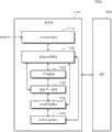
图1是以相关部分示出根据本发明构思的实施例的非易失性存储器装置的框图。参照图1,非易失性存储器装置100包括:存储器单元阵列110、行解码器120、电压发生器电路130、页缓冲器电路140、随机化电路150、输入/输出(I/O)电路160和控制逻辑170。FIG. 1 is a block diagram illustrating a nonvolatile memory device according to an embodiment of the inventive concept in relevant parts. 1, a nonvolatile memory device 100 includes: a
本领域技术人员将认识到,存储器单元阵列110可包括多个存储器块,然而为了清楚起见,在图1中仅仅示出了单个存储器块。假定多个存储器块中的每个存储器块包括多个页。可以不同地定义存储器块内的页。然而,与现代的定义一致,“物理页”在示出的实施例中将被定义为连接到字线的非易失性存储器单元与页标志的集合。此外,与现代的理解一致,非易失性存储器的物理页可包括多个“逻辑页”。然而,物理页通常根据存储器单元的物理实现方式(以及编程到存储器单元的数据或从存储器单元读取的数据)来定义,逻辑页通常根据成组的地址来定义。因此,在包括多级存储器单元(multi-level memory cells,MLC)的阵列的非易失性存储器装置中,物理页可被定义为连接到公共字线的MLC与页标志的集合。多个逻辑页可被存储在单个物理页中。例如,假定在存储器单元阵列中使用2位MLC,则可使用物理页来存储数据的第一或者最低有效位(LSB)页以及数据的第二或者最高有效位(MSB)页。多级非易失性存储器单元(MLC)布置在存储器单元阵列的主区域中,第一页标志和第二页标志被设置在存储器单元阵列的备用区域中,第一页标志和第二页标志连接到公共字线。Those skilled in the art will recognize that
一个物理页111在图1中被具体示为连接到字线WLm-2。One physical page 111 is specifically shown in FIG. 1 as being connected to word line WLm-2.
存储器单元阵列110包括主区域112和备用区域114,因此,遍及存储器单元阵列110的物理页111包括主区域112和备用区域114,其中,主区域112被标识为存储诸如用户定义数据的有效载荷数据,备用区域114被单独地标识为存储存储器管理信息。存储器管理信息可以在存储器系统中被不同地定义,并且可以利用备用区域来进行不同地排列。存储器管理信息可包括例如存储器单元损耗信息、错误校正信息、损坏的存储器单元和替代的存储器单元信息等。可以以物理页为基础、利用各个物理页的备用区域将存储器管理信息存储在物理页中。The
在本发明构思的特定实施例中,存储器管理信息还可包括指示与物理页关联的特定的逻辑页是否已经被编程的信息。例如,在继续提出图1的物理页111包括2位MLC的布置的假定的情况下,存储在备用区域114中的存储器管理信息可包括指示LSB页或者MSB页是否已经被分别编程的信息。In certain embodiments of the inventive concept, the memory management information may further include information indicating whether a specific logical page associated with the physical page has been programmed. For example, the memory management information stored in the spare area 114 may include information indicating whether the LSB page or the MSB page has been respectively programmed, under the assumption that the physical page 111 of FIG. 1 includes a 2-bit MLC arrangement.
可以利用许多不同的数据定义(例如,存储器管理信息的相关位的数量和位置)给出这样的页编程指示。然而,为了简化,下面将假定在存储在备用区域中的存储器管理信息内使用单个位的“页标志”,以指示相应的页编程情况。本领域技术人员将认识到,上下文中的术语“标志”与图1的示例示出的相比覆盖得更为宽广。可以使用多位标志,可以以与以物理页为基础的物理页的基础不同的基础来存储不同的页标志,页标志可以存储在指定的寄存器或者不与数据的物理页关联的存储器中。Such a page programming indication can be given using many different data definitions (eg, number and location of relevant bits of memory management information). However, for simplicity, it will be assumed below that a single-bit "page flag" is used within the memory management information stored in the spare area to indicate a corresponding page programming situation. Those skilled in the art will recognize that the term "logo" in this context has a broader coverage than that shown by the example of FIG. 1 . Multi-bit flags can be used, different page flags can be stored on a different basis than the physical page basis, and the page flags can be stored in designated registers or memory not associated with the physical page of data.
然而,回到图1,备用区域114包括第一标志单元区域115和第二标志单元区域116。第一标志单元区域115包括存储指示物理页111的LSB页的编程状态的信息的存储器单元(下面称为第一标志单元)。第二标志单元区域116包括存储指示物理页111的MSB页的编程状态的存储器单元(下面称为第二标志单元)。在一个示例中,公开的第2009/0180323号美国专利申请提供对存储器单元阵列的备用区域的详细描述,其主题通过引用被包含于此。However, returning to FIG. 1 , the spare area 114 includes a first flag cell area 115 and a second flag cell area 116 . The first flag cell region 115 includes memory cells (hereinafter referred to as first flag cells) storing information indicating a program state of the LSB page of the physical page 111 . The second flag cell region 116 includes memory cells (hereinafter referred to as second flag cells) storing a program state indicating the MSB page of the physical page 111 . In one example, published US Patent Application No. 2009/0180323, the subject matter of which is incorporated herein by reference, provides a detailed description of spare regions of memory cell arrays.
因此,在图1示出的实施例中,第一标志单元存储指示指向物理页111的LSB编程操作的数据。例如,响应于LSB编程操作,第一标志单元可用于存储数据值“0”。换句话说,在LSB编程操作期间,“0”可被编程到第一标志单元。此后,存储在第一标志单元中的(例如,作为可以在读取操作期间被读取的)数据值“0”指示已经与物理页111相关地执行了LSB编程操作。Therefore, in the embodiment shown in FIG. 1 , the first flag cell stores data indicating an LSB program operation directed to the physical page 111 . For example, the first flag cell may be used to store a data value of "0" in response to an LSB program operation. In other words, "0" may be programmed to the first flag cell during the LSB program operation. Thereafter, a data value of "0" stored in the first flag cell (eg, as may be read during a read operation) indicates that an LSB program operation has been performed in relation to the physical page 111 .
类似地,第二标志单元可用于指示已经与物理页111相关地执行了MSB编程操作。例如,响应于MSB编程操作,第二标志单元可用于存储数据值“0”。换句话说,在MSB编程操作期间,“0”可被编程到第二标志单元。此后,存储在第二标志单元中的(例如,作为可在读取操作期间被读取的)数据值“0”指示已经与物理页111相关地执行了MSB编程操作。Similarly, the second flag unit may be used to indicate that an MSB program operation has been performed in relation to the physical page 111 . For example, the second flag cell may be used to store a data value of "0" in response to an MSB program operation. In other words, "0" may be programmed into the second flag cell during the MSB program operation. Thereafter, a data value of "0" stored in the second flag cell (eg, as readable during a read operation) indicates that an MSB program operation has been performed in relation to the physical page 111 .
在图1的存储器单元阵列110中,与字线WL0到WLm-3以及字线WLm-1关联的物理页可以以与物理页111基本相似的方式来布置。In
在图1中示出的实施例中,假定存储器单元阵列110是NAND闪速存储器单元阵列。这样,形成存储器单元阵列的每个存储器块包括多个NAND闪速存储器单元串。每个单元串包括与串选择线SSL连接的串选择晶体管、分别与多条字线WL0到WLm-1中的一条字线连接的多个存储器单元以及与地选择线GSL连接的地选择晶体管,其中,“m”是大于等于2的整数。相应的串选择晶体管与多条位线BL0到BLn-1、1FBL1到1FBLi以及2FBL1到2FBLj连接,其中,“n”是大于等于2的整数,“i”和“j”分别是正整数。相应的地选择晶体管与公共源极线CSL连接。在某些实施例中,公共源极线CSL可被供应有来自CSL驱动器(未示出)的地电压或者CSL电压(例如,电源电压VDD)。In the embodiment shown in FIG. 1, it is assumed that the
行解码器120经由选择线SSL和GSL以及多条字线WL0到WLm-1与存储器单元阵列110连接。行解码器120可被配置为响应于输入的地址ADDR来选择所述多个存储器块中的一个存储器块,并将控制电压(例如,被定义的偏置电压)施加到所选择的存储器块的字线WL0到WLm-1。这样的控制电压可包括但不限于编程电压、通过电压(pass voltage)、校验电压(verificationvoltage)、读取电压、读取通过电压和擦除电压。The
电压发生器电路130被配置为产生执行非易失性存储器装置100的操作所需要的偏置电压。电压发生器电路130产生的偏置电压可通过行解码器120施加到存储器单元阵列110或者相关的电路。虽然没有在图1中示出,但是电压发生器电路130可包括高电压发生器、低电压发生器和负电压发生器。The
页缓冲器电路140与存储器单元阵列110通过多条位线BL0到BLn-1、1FBL1到1FBLi以及2FBL1到2FBLj连接。页缓冲器电路140可被选择性地配置成在编程操作期间临时存储将被编程到被选择的逻辑页的“写数据”,或者在读取操作期间临时存储从被选择的逻辑页取回(retrieve)的“读数据”。The
在图1中示出的特定实施例中,页缓冲器电路140包括主页缓冲器142和备用页缓冲器144。主页缓冲器142包括分别连接到位线BL0到BLn-1的页缓冲器PB0到PBn-1。备用页缓冲器144包括分别与第一页标志位线1FBL1到1FBLi连接的页缓冲器1FPB1到1FPBi(以下称为第一页标志缓冲器)以及分别与第二页标志位线2FBL1到2FBLj连接的页缓冲器2FPB1到2FPBj(以下称为第二页标志缓冲器)。页缓冲器PB0到PBn-1、1FPB1到1FPBi以及2FPB1到2FPBj中的每个页缓冲器可以与一条位线连接,或者与两条或更多条的位线连接。如通常所理解的,前一种连接方式是全位线架构(all bitline architecture),后一种方式是屏蔽位线架构(shield bit line architecture)。In the particular embodiment shown in FIG. 1 ,
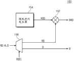
随机化电路150包括能够在编程操作期间使进入的写数据(D)随机化以产生随机化的写数据(RD)且在读取操作期间选择性地使出去的读数据去随机化(de-randomize)或者不使输出的读数据去随机化的电路。因此,随机化电路可包括独立的随机化电路和去随机化电路或者被配置为选择性地执行随机化/去随机化功能的电路。可通过由控制逻辑170提供的随机化选择信号RSEL来控制随机化电路150的一个操作接一个操作的功能。The
因此,随机化电路150可以响应于随机化选择信号RSEL而导通(或启用)和截止(停用)。如在下面将以某些补充的细节进行描述的,可以(至少部分地)通过特定的确定来控制在读取操作期间的随机化选择信号RSEL的启用/停用,所述特定的确定是有关一个或者多个页编程操作(例如,LSB编程或MSB编程操作)是否已经与被标识的读数据相关地执行了的确定。本发明构思的其他实施例可在编程操作期间启用/停用随机化电路150的操作,但是为了便于下面的解释,将假定进入的写数据在经由页缓冲器电路140的主页缓冲器142被存储到存储器单元阵列110之前总是被随机化。Therefore, the
然而,在读取操作期间,可从存储器单元阵列110中取回未被随机化的读数据(D)和被随机化的读数据(RD)这两种类型的读数据中的任一种。因此,随机化电路150必须在被随机化的读数据被提供到I/O电路160之前将被随机化的读数据去随机化,以产生去随机化的读数据(DRD),或者在(正常)的读数据(D)被提供到I/O电路160时不将(正常)的读数据(D)去随机化。换句话说,读数据(D)实质上绕过(bypass)了随机化电路150。可根据组成的非易失性存储器装置的本性和预期用途来不同地实现随机化电路150。然而,在公开的第2010/0229001号美国专利申请和第2010/0229007号美国专利申请中公开了可用的随机化电路的一个示例,所述申请的全部主题通过引用被包含于此。However, during a read operation, either of two types of read data, non-randomized read data (D) and randomized read data (RD), may be retrieved from the
I/O电路160可被选择性地配置为在编程操作期间将从外部装置(例如,主机或者存储器控制器)接收的进入的写数据(D)提供给随机化电路150,或者在读取操作期间将来自随机化电路150的读数据(DRD或D)提供到外部装置。应当注意,这里使用的术语“读取操作”表示意图将来自非易失性存储器装置的读数据提供到外部电路的任意的输出操作,术语“编程操作”表示意图将从外部提供的写数据存储在非易失性存储器装置中的任意的输入操作。I/
控制逻辑170控制非易失性存储器100的总体操作。控制逻辑170分析所接收到的由外部装置提供的控制信号和/或命令(未示出)。响应于这些控制信号和命令,控制逻辑170相互影响式地(inter-operatively)控制行解码器120、电压发生器电路130、页缓冲器电路140、随机化电路150和I/O电路160。The control logic 170 controls the overall operation of the nonvolatile memory 100 . The control logic 170 analyzes received control signals and/or commands provided by external devices (not shown). In response to these control signals and commands, control logic 170 inter-operatively controls row
在图1中示出的实施例中,控制逻辑170包括随机化确定电路172。在读取操作和编程操作期间,随机化确定电路172可被配置为询问(或确定)存储在第一标志单元区域115和第二标志单元区域116中的数据值。然后可与该确定相关地控制随机化电路150的启用/停用。如上所述,第一标志单元区域115存储指示是否已经执行了物理页的LSB编程的信息,第二标志单元区域116存储指示是否已经执行了物理页的MSB编程的信息。In the embodiment shown in FIG. 1 , control logic 170 includes randomization determination circuitry 172 . During read operations and program operations, the randomization determination circuit 172 may be configured to interrogate (or determine) data values stored in the first flag cell region 115 and the second flag cell region 116 . Activation/deactivation of the
在编程操作和读取操作期间,随机化确定电路172可接收来自第一页标志缓冲器1FB1到1FBi的数据并根据多数决定法(majority decision)来确定是否已经执行了物理页的LSB编程,所述第一页标志缓冲器1FB1到1FBi存储从第一标志单元区域115读取的数据。在编程操作或读取操作期间,随机化确定电路172可接收来自第二页标志缓冲器2FPB1到2FPBj的数据并根据多数决定法来确定是否已经执行了物理页的MSB编程,所述第二页标志缓冲器2FPB1到2FPBj存储从第二标志单元区域116读取的数据。然后,随机化确定电路172可基于是否已经执行了物理页的LSB编程和/或MSB编程来产生合适的(启用的或者停用的)随机化选择信号RSEL。During the program operation and the read operation, the randomization determination circuit 172 may receive data from the first page flag buffers 1FB1 to 1FBi and determine whether the LSB programming of the physical page has been performed according to a majority decision, so The first page flag buffers 1FB1 to 1FBi store data read from the first flag cell area 115 . During a program operation or a read operation, the randomization determination circuit 172 may receive data from the second page flag buffers 2FPB1 to 2FPBj and determine whether MSB programming of a physical page has been performed according to a majority decision. The flag buffers 2FPB1 to 2FPBj store data read from the second flag cell area 116 . The randomization determination circuit 172 may then generate the appropriate (enabled or disabled) randomization selection signal RSEL based on whether LSB programming and/or MSB programming of the physical page has been performed.
如本领域技术人员将容易理解的,可通过分配对应的逻辑电平来指示随机化选择信号RSEL(或任意其他控制信号)的状态(启用/停用)。相应地,可向逻辑电平分配给定的电压电平(例如,地或者某电源电压电平)。这些逻辑电平(和对应的电压)的指定(或定义)是设计选择的问题。因此,在下面的描述中,在可交替地使用相反的逻辑电平的理解下,控制信号(比如随机化选择信号RSEL)的启用状态/停用状态可被任意地定义为逻辑“低”或“高”。As will be readily understood by those skilled in the art, the state (enabled/disabled) of the randomization selection signal RSEL (or any other control signal) may be indicated by assigning a corresponding logic level. Accordingly, logic levels may be assigned a given voltage level (eg, ground or some supply voltage level). The specification (or definition) of these logic levels (and corresponding voltages) is a matter of design choice. Therefore, in the following description, the enabled state/disabled state of a control signal (such as the randomization selection signal RSEL) can be arbitrarily defined as logic "low" or "high".
在参照图1描述的实施例中,假定在因随机化确定电路172的操作而产生高的随机化选择信号RSEL时,随机化电路150将工作以使进入的写数据随机化,或者使出去的读数据去随机化。当因随机化确定电路172的操作而产生低的随机化选择信号RSEL时,随机化电路150在绕过模式下操作,以不使读数据去随机化。In the embodiment described with reference to FIG. 1 , it is assumed that when the randomization selection signal RSEL is high due to the operation of the randomization determination circuit 172, the
本领域技术人员将理解,期望将随机化的写数据存储在存储器单元阵列110内。因此,根据本发明构思的实施例的非易失性存储器装置因遍及形成存储器单元阵列110的非易失性存储器单元的矩阵来进行基本上被随机化的写数据的编程而受益。因此,以物理页为基础来存储随机化的写数据,以使在串或列方向以及字线或行方向上的存储器单元的各个阈值电压均匀分布。存储器单元阈值电压的这样的遍及整个存储器单元阵列的均匀分布有助于减小存储器单元的相互干扰并改善读取裕度(read margin)。Those skilled in the art will appreciate that it is desirable to store randomized write data within
尽管期望保持遍及存储器单元阵列的“随机化的数据”的基本均匀的分布,但是使新的(即,之前从未编程过的)非易失性存储器装置具有被合理地(已知的或可解的)随机化的存储的数据状态是无法实施的。除了导致明显的无法实施性的其他约束之外,这样的情况还应以每名消费者使用或熟知的通用的随机化/去随机化方案为前提。结果,新的非易失性存储器单元阵列通常具有全部被置于(缺省的)擦除状态的存储器单元。此后,直到被用户第一次编程为止,非易失性存储器单元一直保持擦除状态。While it is desirable to maintain a substantially uniform distribution of "randomized data" throughout an array of memory cells, it is reasonable (known or possible) to have a new (i.e., never programmed before) nonvolatile memory device solution) Randomizing the stored data state is not possible. Such a situation should presuppose a common randomization/de-randomization scheme used or known by each consumer, in addition to other constraints leading to apparent impossibility. As a result, a new array of non-volatile memory cells typically has memory cells all placed in the (default) erased state. Thereafter, the non-volatile memory cells remain in an erased state until programmed for the first time by the user.
根据本发明构思的实施例的包括MLC的特定的非易失性存储器装置利用对应的页编程操作(例如,2位的MLC的LSB编程和MSB编程),以逻辑页为基础,将多级(multi-level)写数据存储在逻辑页上。一个或更多的逻辑页可以已经在先前被编程或在先前没有被预先编程。因此,在随后的读取操作期间,非易失性存储器装置必须能够确定什么时候使已经在先前被编程并因而被随机化的读数据去随机化、以及什么时候不使在先前没有被编程并因而未被随机化的读数据去随机化。因此,可以根据关于是否已经在先前对特定的逻辑数据页进行了编程的确定,来实现控制逻辑选择性地启用/停用随机化电路。通过这种方式,可以在读取操作期间防止随机化电路的从存储器单元阵列取回的与不同类型的读数据(D与RD)有关的错误的操作。A specific nonvolatile memory device including an MLC according to an embodiment of the inventive concept utilizes a corresponding page programming operation (for example, LSB programming and MSB programming of a 2-bit MLC), on a logical page basis, multi-level ( multi-level) write data is stored on logical pages. One or more logical pages may have been previously programmed or not previously pre-programmed. Therefore, during a subsequent read operation, the nonvolatile memory device must be able to determine when to derandomize read data that has been previously programmed and thus randomized, and when not to derandomize read data that was not previously programmed and thus randomized. Read data that was not randomized is thus de-randomized. Accordingly, control logic may be implemented to selectively enable/disable the randomization circuit based on a determination as to whether a particular page of logical data has been previously programmed. In this way, erroneous operation of the randomization circuit relating to different types of read data (D and RD) retrieved from the memory cell array can be prevented during a read operation.
如上面所提到的,本领域技术人员还将认识到,可以利用各种技术以及对应的电路和/或软件来完成数据的随机化和去随机化。图2是进一步示出在读取操作期间图1的随机化电路150的操作的一个可能的模式的框图。参照图2,随机化电路150包括逻辑运算器152、随机序列发生器154和选择器156。As mentioned above, those skilled in the art will also recognize that randomization and de-randomization of data can be accomplished using various techniques and corresponding circuitry and/or software. FIG. 2 is a block diagram further illustrating one possible mode of operation of the
逻辑运算器152通过使随机化的数据(RD)与随机序列数据(RSD)进行异或运算来使随机化的数据(RD)去随机化。随机化的数据(RD)的块大小可以根据被使用的去随机化方案而与随机序列数据(RSD)相同或不相同。如果随机化的数据RD具有数据(D)与随机序列数据(RSD)的异或值,则去随机化的数据(DRD)是未被随机化的源数据(D)。这可以通过下面的等式来表达,其中符号
随机序列发生器154在读取操作期间基于至少一个种子值来产生随机序列数据RSD。在图2示出的实施例中,所述至少一个种子值可以根据恒定值或者与读数据有关的地址来形成,其中,地址可指示逻辑页和/或物理页。在随机序列发生器154使用恒定值的情况下,恒定值可以存储在非易失性存储器装置100内的寄存器或存储器中。可不同地实现随机序列发生器154。然而,在公开的第2010/0259983号美国专利申请中阐述了一个可能的实施方式的示例,所述申请的主题被包含于此。The
可以将图2中示出的逻辑运算器152设置在图1的页缓冲器电路内。The
响应于随机化选择信号RSEL,选择器156确定从页缓冲器电路140的主页缓冲器142提供的随机化的数据(RD)或者未被随机化的数据(D)是否应该被提供到逻辑运算器152或者绕过逻辑运算器152直接提供到I/O电路160。In response to the randomization selection signal RSEL, the
利用图2中示出的配置,随机化电路150响应于随机化选择信号RSEL,以使随机化的数据(RD)去随机化或者使未被随机化的数据绕过。因此,可以防止随机化电路150在读取操作期间的异常的操作。With the configuration shown in FIG. 2, the
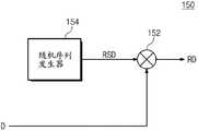
图3是进一步示出图1的随机化电路150在编程操作期间的操作的一个可能的模式的框图。参照图3,随机化电路150操作,以通过使在编程操作期间的写数据与随机序列发生器154提供的随机序列数据(RSD)进行异或运算来使进入的写数据(D)随机化。可直接从I/O电路160接收写数据(D)。可选择地,可通过图2的在编程操作期间响应于随机化选择信号RSEL而操作的选择器156来提供写数据(D)。换句话说,选择器156可在读取操作和编程操作期间均被使用。由图3的逻辑运算器152提供的随机化的数据(RD)可被提供到页缓冲器电路140的主页缓冲器142。FIG. 3 is a block diagram further illustrating one possible mode of operation of the
如与在图2和图3中示出的实施例相关地示出的,可利用单个逻辑运算器152和单个随机序列发生器154有效地实现执行随机化功能和去随机化功能的随机化电路。然而,本领域技术人员将认识到,可使用许多不同的电路来提供随机化的和/或去随机化的功能。As shown in relation to the embodiments shown in FIGS. 2 and 3 , a randomization circuit that performs randomization and de-randomization functions can be efficiently implemented with a
如前面所提到的,可使用根据本发明构思的实施例的非易失性存储器装置,以根据与物理页关联的多个(2个或更多个)逻辑页对MLC编程。此后,为了便于描述,假定两(2)个逻辑页与在物理页布置中的连接到字线的两位的MLC关联。两个逻辑页包括存储LSB数据的第一页或LSB页以及存储MSB数据的第二页或MSB页。As mentioned earlier, a nonvolatile memory device according to embodiments of the inventive concept may be used to program an MLC according to a plurality (2 or more) of logical pages associated with a physical page. Hereinafter, for convenience of description, it is assumed that two (2) logical pages are associated with a two-bit MLC connected to a word line in a physical page arrangement. The two logical pages include a first page or LSB page storing LSB data and a second page or MSB page storing MSB data.
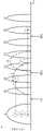
在上下文中,本领域技术人员将进一步认识到,对连接到一条字线的MLC的编程可干扰连接到相邻的字线的MLC的编程状态,从而减小了读取裕度。为了减小这样的干扰,根据本发明构思的实施例的某些非易失性存储器装置可根据避免顺序的页编程(或使顺序的页编程最少化)的逻辑页和/或物理页的顺序而被编程。在这点上,可定义许多不同的页编程“顺序”。In this context, those skilled in the art will further appreciate that programming an MLC connected to one word line can disturb the programmed state of an MLC connected to an adjacent word line, thereby reducing read margin. In order to reduce such interference, some nonvolatile memory devices according to embodiments of the inventive concept may be based on the order of logical pages and/or physical pages that avoid (or minimize) sequential page programming. And be programmed. In this regard, many different page programming "sequences" can be defined.
图4是示出可在本发明构思的某些实施例中使用的一个示例性的页编程顺序的概念性示图。如图4中示出,与第一字线WL0关联的第一逻辑页(FLP)“0”被编程,然后与第二字线WL1关联的FLP“1”被编程。然后,与第一字线WL0关联的第二逻辑页(SLP)“2”被编程,与第三字线WL2关联的FLP“3”被编程。FLP和SLP可以以交错的顺序(SLP跟随FLP)被编程,以避免或者最小化相邻的MLC干扰。FLP和SLP的顺序化布置可利用从对应的逻辑地址得出的值来指定,并且可根据页编程序列来确定。FIG. 4 is a conceptual diagram illustrating an exemplary page programming sequence that may be used in some embodiments of the inventive concept. As shown in FIG. 4, a first logical page (FLP) "0" associated with a first word line WL0 is programmed, and then a FLP "1" associated with a second word line WL1 is programmed. Then, the second logical page (SLP) "2" associated with the first word line WL0 is programmed, and the FLP "3" associated with the third word line WL2 is programmed. FLP and SLP can be programmed in a staggered order (SLP follows FLP) to avoid or minimize adjacent MLC interference. The sequential placement of FLPs and SLPs can be specified with values derived from corresponding logical addresses, and can be determined from a page programming sequence.
图4中示出的页编程顺序(或页编程序列)仅仅是一个示例。本发明构思的实施例可使用许多不同的页编程顺序。The page programming order (or page programming sequence) shown in FIG. 4 is just one example. Embodiments of the inventive concept may use many different page programming sequences.
图5A是示出由第一页(或LSB)编程操作得到的阈值电压分布的概念性示图。图5B是示出根据本发明构思的某些实施例的由第二页(或MSB)编程操作获得的阈值电压分布的概念性示图。FIG. 5A is a conceptual diagram illustrating threshold voltage distributions resulting from a first page (or LSB) program operation. FIG. 5B is a conceptual diagram illustrating threshold voltage distributions obtained by a second page (or MSB) program operation according to some embodiments of the inventive concept.
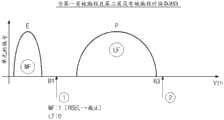
参照图5A,根据第一页编程的阈值电压分布包括擦除状态E和“临时的”编程状态P。在特定的实施例中,擦除状态E可对应于数据值“1”,临时编程状态P可对应于数据值“0”,但是这也可以是其他的情况。第一读取电压R1可被用于区分擦除状态E和临时编程状态P。Referring to FIG. 5A, the threshold voltage distribution programmed according to the first page includes an erased state E and a "temporary" programmed state P. Referring to FIG. In a particular embodiment, the erased state E may correspond to a data value of "1" and the temporary programmed state P may correspond to a data value of "0," but this may be the case otherwise. The first read voltage R1 may be used to distinguish the erase state E from the temporary program state P.
参照图5B,根据第二页编程的阈值电压分布包括擦除状态E、第一编程状态P1、第二编程状态P2和第三编程状态P3。在该实施例中,擦除状态E可对应于数据值“11”,第一编程状态P1对应于数据值“01”,第二编程状态P2对应于数据值“00”,第三编程状态P3对应于数据值“10”,但是这也可以是其他的情况。第一读取电压R1可用于区分擦除状态E与第一编程状态P1,第二读取电压R2可用于区分第一编程状态P1和第二编程状态P2,第三读取电压R3可用于区分第二编程状态P2和第三编程状态P3。Referring to FIG. 5B, the threshold voltage distribution programmed according to the second page includes an erased state E, a first programmed state P1, a second programmed state P2, and a third programmed state P3. In this embodiment, the erased state E may correspond to the data value "11", the first programmed state P1 may correspond to the data value "01", the second programmed state P2 may correspond to the data value "00", and the third programmed state P3 corresponds to the data value "10", but this could also be the case otherwise. The first read voltage R1 can be used to distinguish the erased state E from the first programmed state P1, the second read voltage R2 can be used to distinguish the first programmed state P1 from the second programmed state P2, and the third read voltage R3 can be used to distinguish The second programming state P2 and the third programming state P3.
参照图1,根据本发明构思的实施例的非易失性存储器100响应于第一页编程操作对第一页(或LSB)标志编程,响应于第二页编程操作对第二页(或MSB)标志编程。第一标志单元区域115中的“置位的”LSB标志指示已经执行了LSB编程,第二标志单元区域116中的置位的MSB标志指示已经执行了MSB编程。多级非易失性存储器单元被配置为在将第一页数据编程到多级非易失性存储器单元时被选择性地编程为临时状态,且在将第二页数据编程到多级非易失性存储器单元时被选择性地编程为多个编程状态中的一个编程状态。Referring to FIG. 1, a nonvolatile memory 100 according to an embodiment of the inventive concept programs a first page (or LSB) flag in response to a first page program operation, and programs a second page (or MSB) flag in response to a second page program operation. ) flag programming. A "set" LSB flag in the first flag cell area 115 indicates that LSB programming has been performed, and a set MSB flag in the second flag cell area 116 indicates that MSB programming has been performed. The multi-level nonvolatile memory cells are configured to be selectively programmed to a temporary state when programming a first page of data into the multilevel nonvolatile memory cells, and to be selectively programmed to a temporary state when programming a second page of data into the multilevel nonvolatile memory cells. The volatile memory cells are selectively programmed to one of a plurality of programming states.
图6A是根据本发明构思的实施例的概述用于图1的非易失性存储器装置的一个可能的LSB标志编程方法的流程图。同时参照图1、图5A和图6A,控制逻辑170首先确定访问存储器单元阵列110的请求的操作是否是第一页编程操作(S110)。可根据与编程操作相关联的写地址来确定请求的操作是否是第一页编程操作。例如,如图4中所示,奇数地址可用于指示请求的编程操作是第一页编程操作。FIG. 6A is a flowchart outlining one possible LSB flag programming method for the nonvolatile memory device of FIG. 1 according to an embodiment of the inventive concept. Referring to FIGS. 1 , 5A and 6A simultaneously, the control logic 170 first determines whether a requested operation to access the
如果请求的操作被确定为是第一页编程操作(S110=是),则第一标志区域115中的LSB标志被编程为临时的编程状态P(S120)。然而,如果请求的操作不是第一页编程操作(S110=否),则该方法跳过对LSB标志的编程。If the requested operation is determined to be the first page program operation (S110=Yes), the LSB flag in the first flag area 115 is programmed to a temporary program state P (S120). However, if the requested operation is not the first page program operation (S110=No), the method skips programming the LSB flag.
接下来,控制逻辑170确定请求的操作是否是第二页编程操作(S130)。这里可以再次与对应的地址相关地确定请求的操作是否是第二页编程操作。例如,如图4中所示,可使用偶数地址来指示请求的操作是第二页编程操作。如果请求的操作被确定是第二页编程操作(S130=是),则LSB标志是禁止编程的(S165)。然而,如果请求的操作被确定为不是第二页编程操作,则所述方法终止。Next, the control logic 170 determines whether the requested operation is a second page program operation (S130). Here again it may be determined in relation to the corresponding address whether the requested operation is a second page program operation. For example, as shown in FIG. 4, an even address may be used to indicate that the requested operation is a second page program operation. If the requested operation is determined to be the second page program operation (S130=YES), the LSB flag is program inhibited (S165). However, if the requested operation is determined not to be a second page programming operation, the method terminates.
利用图6A的LSB标志编程方法,可以响应于第一页编程操作将LSB标志编程为临时状态P,同时响应于第二页编程操作,LSB标志是禁止编程的。然而,可使用其他的方法来响应于第一(或LSB)页编程将LSB标志适当地置位/复位。Using the LSB flag programming method of FIG. 6A, the LSB flag can be programmed to the temporary state P in response to the first page program operation, while the LSB flag is program-inhibited in response to the second page program operation. However, other methods can be used to properly set/reset the LSB flag in response to the first (or LSB) page programming.
图6B是根据本发明构思的实施例的概述用于图1的非易失性存储器装置的一个可能的LSB标志编程方法的流程图。同时参照图1、图5A、图5B和图6B,控制逻辑170首先确定访问存储器单元阵列的请求的操作是否是第一页编程操作(S110)。可根据对应的地址来确定请求的操作是否是第一页编程操作。例如,如图4中所示,奇数地址可用于指示请求的操作是第一页编程操作。FIG. 6B is a flowchart outlining one possible LSB flag programming method for the nonvolatile memory device of FIG. 1 according to an embodiment of the inventive concept. Referring to FIGS. 1 , 5A, 5B, and 6B simultaneously, the control logic 170 first determines whether a requested operation to access the memory cell array is a first page program operation ( S110 ). Whether the requested operation is a first page program operation may be determined according to the corresponding address. For example, as shown in FIG. 4, an odd address may be used to indicate that the requested operation is a first page program operation.
如果请求的操作被确定为是第一页编程操作(S110=是),则第一标志区域115中的LSB标志被编程为临时的编程状态P(S120)。然而,如果请求的操作不是第一页编程操作,则跳过对LSB标志的编程。If the requested operation is determined to be the first page program operation (S110=Yes), the LSB flag in the first flag area 115 is programmed to a temporary program state P (S120). However, if the requested operation is not a first page program operation, then programming the LSB flag is skipped.
接下来,控制逻辑170确定请求的操作是否是第二页编程操作(S130)。这里可以再次根据对应的地址来确定请求的操作是否是第二页编程操作。例如,如图4中所示,可使用偶数地址来指示请求的操作是第二页编程操作。Next, the control logic 170 determines whether the requested operation is a second page program operation (S130). Here again, it may be determined according to the corresponding address whether the requested operation is the second page programming operation. For example, as shown in FIG. 4, an even address may be used to indicate that the requested operation is a second page program operation.
如果请求的操作被确定是第二页编程操作(S130=是),则控制逻辑170确定与由第二页编程操作标识的第二页数据关联的第一页数据是否已经在先前被编程(S140)。可通过读取第一标志单元区域中的一个或多个第一页标志的值来确定第一页是否已经被编程。如果请求的操作不是第二页编程操作,则该方法终止。If the requested operation is determined to be a second page programming operation (S130=Yes), the control logic 170 determines whether the first page data associated with the second page data identified by the second page programming operation has been previously programmed (S140 ). Whether the first page has been programmed can be determined by reading the values of one or more first page flags in the first flag cell area. If the requested operation is not a second page program operation, the method terminates.
现在,如果确定已经对第一页编程(S140=是),则LSB标志被编程为(或从临时编程状态P再次被编程为)多个编程状态中的一个编程状态(P1、P2或P3)(例如,图6B的示例中的第二编程状态P2)(S150)。然而,如果确定第一页没有被编程(即,LSB标志具有擦除状态)(S140=否),则LSB标志是禁止编程的(S160)。Now, if it is determined that the first page has been programmed (S140=Yes), the LSB flag is programmed (or programmed again from the temporary programming state P) to one of the programming states (P1, P2 or P3) (eg, the second programming state P2 in the example of FIG. 6B) (S150). However, if it is determined that the first page is not programmed (ie, the LSB flag has an erased state) (S140=No), the LSB flag is program-inhibited (S160).
如上所描述的,根据LSB标志编程方法,响应于第一页编程操作将LSB标志编程为具有临时的编程状态P,响应于第二页编程操作将LSB标志编程为具有多个编程状态中的一个编程状态(例如,P2或P3)。As described above, according to the LSB flag programming method, the LSB flag is programmed to have a temporary program state P in response to the first page program operation, and is programmed to have one of a plurality of program states in response to the second page program operation. programming state (eg, P2 or P3).
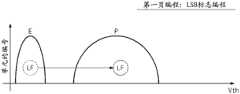
图7是示出响应于第一(或LSB)标志编程方法得到的页标志状态和阈值电压分布的概念性示图。参照图7,响应于第一页编程操作将LSB标志(LF)编程为临时编程状态P。FIG. 7 is a conceptual diagram illustrating page flag states and threshold voltage distributions in response to a first (or LSB) flag programming method. Referring to FIG. 7, the LSB flag (LF) is programmed to the temporary program state P in response to the first page program operation.
图8是示出在没有执行第一页编程的条件下响应于第二页编程操作得到的页标志状态和阈值电压分布的概念性示图。参照图8,在尚未执行第一页编程操作的条件下,响应于第二页编程操作,LSB标志LF是禁止编程的。这意味着LSB标志LF具有擦除状态E。FIG. 8 is a conceptual diagram illustrating page flag states and threshold voltage distributions obtained in response to a second page program operation under the condition that the first page program is not performed. Referring to FIG. 8, the LSB flag LF is program-inhibited in response to the second page program operation under the condition that the first page program operation has not been performed. This means that the LSB flag LF has an erased state E.
图9A是示出在执行了第一页编程操作之后响应于第二页编程操作而得到的页标志状态和阈值电压分布的概念性示图。参照图9A,在已经执行了第一页编程操作的条件下,响应于第二页编程操作,LSB标志LF是禁止编程的。FIG. 9A is a conceptual diagram illustrating page flag states and threshold voltage distributions obtained in response to a second page program operation after the first page program operation is performed. Referring to FIG. 9A , the LSB flag LF is program-inhibited in response to the second page program operation under the condition that the first page program operation has been performed.
图9B是示出响应于在执行第一页编程操作之后执行的第二页编程操作而得到的页标志状态和阈值电压分布的概念性示图。参照图9B,在已经执行了第一页编程操作的条件下,LSB标志LF从临时编程状态P被(再次)编程为第二编程状态P2。FIG. 9B is a conceptual diagram illustrating page flag states and threshold voltage distributions in response to a second page program operation performed after performing a first page program operation. Referring to FIG. 9B , under the condition that the first page program operation has been performed, the LSB flag LF is (re)programmed from the temporary program state P to the second program state P2.
图10是概述用于图1的非易失性存储器装置的MSB标志编程方法的流程图。将同时参照图1、图5A、图5B和图10来描述MSB标志编程方法。FIG. 10 is a flowchart outlining an MSB flag programming method for the nonvolatile memory device of FIG. 1 . The MSB flag programming method will be described with reference to FIG. 1 , FIG. 5A , FIG. 5B , and FIG. 10 simultaneously.
首先,控制逻辑170确定请求的操作是否是第一页编程操作(S210)。如果请求的操作是第一页编程操作(S110=是),则MSB标志是禁止编程的(S220)。然而,如果请求的操作不是第一页编程操作,则跳过对MSB标志的禁止编程。First, the control logic 170 determines whether the requested operation is a first page program operation (S210). If the requested operation is a first page program operation (S110=Yes), the MSB flag is program inhibited (S220). However, if the requested operation is not a first page program operation, the program inhibit for the MSB flag is skipped.
然后,控制逻辑170确定请求的操作是否是第二页编程操作(S230)。如果请求的访问是第二页编程操作(S230=是),则将MSB标志编程为多个编程状态中的一个编程状态(例如,第二编程状态P2或第三编程状态P3)(S240)。然而,如果请求的操作不是第二页编程操作,则所述方法终止。Then, the control logic 170 determines whether the requested operation is a second page program operation (S230). If the requested access is a second page program operation (S230=Yes), the MSB flag is programmed to one of a plurality of program states (eg, the second program state P2 or the third program state P3) (S240). However, if the requested operation is not a second page program operation, the method terminates.
如上所述,MSB标志编程方法包括响应于第一页编程操作禁止编程MSB标志以及响应于第二页编程操作将MSB标志编程为第二编程状态P2。As described above, the MSB flag programming method includes inhibiting programming of the MSB flag in response to the first page program operation and programming the MSB flag to the second program state P2 in response to the second page program operation.
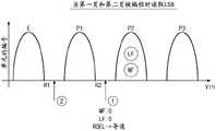
图11是示出在尚未执行第一页编程操作的条件下响应于MSB标志编程方法和第二页编程操作而得到的页标志状态和阈值电压分布的概念性示图。参照图11,响应于第二页编程操作,MSB标志从擦除状态E被编程为多个编程状态中的一个编程状态(例如,第二编程状态P2)。FIG. 11 is a conceptual diagram illustrating page flag states and threshold voltage distributions obtained in response to the MSB flag programming method and the second page programming operation under the condition that the first page programming operation has not been performed. Referring to FIG. 11 , in response to the second page program operation, the MSB flag is programmed from the erased state E to one of the plurality of program states (eg, the second program state P2 ).
图12A是示出通过图1的非易失性存储器装置的页编程操作得到的标志状态的概念性示图。参照图12A,LSB标志和MSB标志(LF和MF)在第一页和第二页没有被编程的情况下具有擦除状态E。如果第一页被编程,则LSB标志(LF)具有临时编程状态P,MSB标志具有擦除状态E。如果第二页被编程,则LSB标志(LF)是禁止编程的,MSB标志具有第二编程状态P2或第三编程状态P3,其中,第二编程状态P2或第三编程状态P3的阈值电压的电平大于临时编程状态P的阈值电压的电平。FIG. 12A is a conceptual diagram illustrating flag states obtained through a page program operation of the nonvolatile memory device of FIG. 1 . Referring to FIG. 12A, the LSB flag and the MSB flag (LF and MF) have an erased state E in the case that the first page and the second page are not programmed. If the first page is programmed, the LSB flag (LF) has a temporary programmed state P and the MSB flag has an erased state E. If the second page is programmed, the LSB flag (LF) is programming inhibited, and the MSB flag has the second programming state P2 or the third programming state P3, wherein the threshold voltage of the second programming state P2 or the third programming state P3 The level is greater than that of the threshold voltage of the temporary programmed state P.
图12B是示出通过图1的非易失性存储器装置的页编程操作得到的标志状态的概念性示图。参照图12B,LSB标志和MSB标志(LF和MF)在第一页和第二页没有被编程的情况下具有擦除状态E。如果第一页被编程,则LSB标志(LF)具有临时的编程状态P,MSB标志具有擦除状态E。如果第二页被编程,则LSB标志(LF)具有第二编程状态P2或第三编程状态P3,MSB标志具有第二编程状态P2或第三编程状态P3,其中,第二编程状态P2或第三编程状态P3的阈值电压的电平大于临时编程状态P的阈值电压的电平。FIG. 12B is a conceptual diagram illustrating flag states obtained through a page program operation of the nonvolatile memory device of FIG. 1 . Referring to FIG. 12B, the LSB flag and the MSB flag (LF and MF) have an erased state E in the case that the first page and the second page are not programmed. If the first page is programmed, the LSB flag (LF) has a temporary programmed state P and the MSB flag has an erased state E. If the second page is programmed, the LSB flag (LF) has the second programming state P2 or the third programming state P3, and the MSB flag has the second programming state P2 or the third programming state P3, wherein the second programming state P2 or the third programming state The level of the threshold voltage of the third programming state P3 is greater than the level of the threshold voltage of the temporary programming state P.
如图12B所描述的,LSB标志LF被编程为具有这样的状态,所述状态具有大于临时编程状态的阈值电压的阈值分布。因此,存储页标志的非易失性存储器单元的被编程的阈值电压将从初始状态增加。As depicted in FIG. 12B , the LSB flag LF is programmed to have a state with a threshold distribution greater than the threshold voltage of the temporary programmed state. Therefore, the programmed threshold voltage of the nonvolatile memory cell storing the page flag will increase from the initial state.
图13是根据本发明构思的另一实施例的概述LSB读取操作的流程图。LSB读取操作通常包括:确定LSB数据的值(S310),然后与存储的LSB标志的值相关地使LSB数据去随机化(S320)。FIG. 13 is a flowchart outlining an LSB read operation according to another embodiment of the inventive concept. An LSB read operation generally includes determining the value of the LSB data (S310), and then de-randomizing the LSB data in relation to the value of the stored LSB flag (S320).
确定LSB数据的值(S310)的步骤以利用控制逻辑170在第一读取阶段(①)通过使用第二读取电压R2来区分LSB数据(S311)作为开始。第一读取阶段可包括:基于对应的读取命令和地址来确定请求的操作是否是LSB读取操作,然后利用第二读取电压R2读取由地址标识的数据页。读取的页可包括指示LSB页和/或MSB页是否已经被编程的第一标志单元115和第二标志单元116。The step of determining the value of the LSB data ( S310 ) begins by using the control logic 170 to distinguish the LSB data ( S311 ) by using the second read voltage R2 in the first read phase (①). The first read phase may include determining whether a requested operation is an LSB read operation based on a corresponding read command and an address, and then reading a data page identified by the address using a second read voltage R2. The read page may include a first flag unit 115 and a second flag unit 116 indicating whether the LSB page and/or the MSB page have been programmed.
即,做出有关MSB标志的阈值电压Vth是否大于第二读取电压R2的电平的确定(S312)。如果尚未对读取的页进行MSB编程,则MSB标志的阈值电压Vth将小于第二读取电压R2的电平。如果已经对读取的页进行了MSB编程,则MSB标志的阈值电压Vth将大于第二读取电压R2的电平。That is, a determination is made as to whether the threshold voltage Vth of the MSB flag is greater than the level of the second read voltage R2 (S312). If the read page has not been MSB programmed, the threshold voltage Vth of the MSB flag will be less than the level of the second read voltage R2. If the read page has been MSB programmed, the threshold voltage Vth of the MSB flag will be greater than the level of the second read voltage R2.
如果MSB标志的阈值电压Vth小于第二读取电压R2(S312=否),则在控制逻辑170的控制下,在第二读取阶段(②)期间,基于第一读取电压R1来读取通过读取地址识别出的LSB页(S313)。If the threshold voltage Vth of the MSB flag is less than the second read voltage R2 (S312=No), under the control of the control logic 170, during the second read phase (②), read based on the first read voltage R1 The LSB page identified by the read address (S313).
即,做出有关LSB页中的存储器单元的阈值电压是否大于第一读取电压R1的确定(S314)。如果存储器单元的阈值电压小于第一读取电压R1(S314=否),则确定数据值“1”(S316)。然而,如果存储器单元的阈值电压大于第一读取电压R1(S314=是),则确定数据值“0”(S317)。That is, a determination is made as to whether the threshold voltage of the memory cells in the LSB page is greater than the first read voltage R1 (S314). If the threshold voltage of the memory cell is less than the first read voltage R1 (S314=NO), the data value '1' is determined (S316). However, if the threshold voltage of the memory cell is greater than the first read voltage R1 (S314=YES), the data value '0' is determined (S317).
如果MSB标志MF的阈值电压大于第二读取电压R2(S312=是),则做出有关每个读取的存储器单元的阈值电压是否大于第二读取电压R2的确定(S315)。如果存储器单元的阈值电压小于第二读取电压R2(S315=否),则确定数据值“1”(S316)。然而,如果存储器单元的阈值电压大于第二读取电压R2(S315=是),则确定数据值“0”(S317)。这样即结束了LSB数据确定步骤(S310)。If the threshold voltage of the MSB flag MF is greater than the second read voltage R2 (S312=YES), a determination is made as to whether the threshold voltage of each read memory cell is greater than the second read voltage R2 (S315). If the threshold voltage of the memory cell is less than the second read voltage R2 (S315=No), the data value '1' is determined (S316). However, if the threshold voltage of the memory cell is greater than the second read voltage R2 (S315=YES), the data value '0' is determined (S317). This ends the LSB data determination step (S310).
如上所描述的,根据本发明构思的示出的实施例中的LSB数据确定操作,存储在存储器单元中的LSB数据通过执行利用第二读取电压R2的第一读取阶段(①)和利用第一读取电压R1的第二读取阶段(②)来确定。这种类型的LSB数据确定操作可被不同地执行,但是在第7,672,162号美国专利中公开了一个可能的方式,其主题通过引用被包含于此。As described above, according to the LSB data determination operation in the illustrated embodiment of the inventive concept, the LSB data stored in the memory cell is obtained by performing the first read phase (①) using the second read voltage R2 and using The second read phase (②) of the first read voltage R1 is determined. This type of LSB data determination operation can be performed differently, but one possible approach is disclosed in US Patent No. 7,672,162, the subject matter of which is incorporated herein by reference.
在LSB数据确定操作(S310)完成之后,根据LSB标志(LF)的存储的值,将LSB数据去随机化或者不将LSB数据去随机化(S320)。这可以不同地完成。将参照图14到图17来描述用于在LSB读取操作期间确定去随机化还是不去随机化的一种方式。如图1中所示,可根据施加的随机化选择信号RSEL来确定随机化功能的启用/停用。即,可以响应于随机化选择信号RSEL来使图1的随机化电路150导通或者截止。After the LSB data determining operation (S310) is completed, the LSB data is de-randomized or not de-randomized (S320) according to the stored value of the LSB flag (LF). This can be done differently. One way to determine whether to derandomize or not to derandomize during an LSB read operation will be described with reference to FIGS. 14 to 17 . As shown in Fig. 1, the activation/deactivation of the randomization function may be determined according to the applied randomization selection signal RSEL. That is, the
图14是示出图1的非易失性存储器装置在尚未对第一页和第二页编程时的LSB读取操作的示图。参照图14,由于没有对第一页和第二页编程,所以LSB标志和MSB标志(LF和MF)分别具有擦除状态E。FIG. 14 is a diagram illustrating an LSB read operation of the nonvolatile memory device of FIG. 1 when the first page and the second page have not been programmed. Referring to FIG. 14, since the first page and the second page are not programmed, the LSB flag and the MSB flag (LF and MF) have an erased state E, respectively.
在LSB读取操作期间,控制逻辑170利用第二读取电压R2读取由对应的地址识别出的页(第一读取阶段①)。此时,读取在第二标志单元区域116中的第二(或MSB)标志单元的数据。由于MSB标志(MF)具有擦除状态E,所以根据多数决定法确定存储在第二标志单元中的数据具有数据值“1”。从上面的描述应当理解,第二页没有被编程。During the LSB read operation, the control logic 170 reads the page identified by the corresponding address using the second read voltage R2 (first read phase ①). At this time, the data of the second (or MSB) flag cell in the second flag cell area 116 is read. Since the MSB flag (MF) has an erased state E, it is determined that the data stored in the second flag unit has a data value of '1' according to a majority decision. It should be understood from the above description that the second page is not programmed.
此后,在LSB读取操作期间,控制逻辑170利用第一读取电压R1读取由对应的地址识别的页(第二读取阶段②)。此时,读取第一标志单元区域115中的第一(或LSB)标志单元的数据。由于LSB标志(LF)具有擦除状态E,所以根据多数决定法确定存储在第一标志单元中的数据具有数据值“1”。Thereafter, during the LSB read operation, the control logic 170 reads the page identified by the corresponding address using the first read voltage R1 (second read phase ②). At this time, the data of the first (or LSB) flag cell in the first flag cell area 115 is read. Since the LSB flag (LF) has an erased state E, it is determined that the data stored in the first flag cell has a data value of '1' according to a majority decision.
由于在LSB读取操作期间确定了第一页和第二页没有被编程,所以控制逻辑170的随机化确定电路172截止或者停用施加到随机化电路150的随机化选择信号RSEL。Since it was determined during the LSB read operation that the first page and the second page were not programmed, the randomization determination circuit 172 of the control logic 170 turns off or disables the randomization selection signal RSEL applied to the
通过上面的描述可以理解,当第一页和第二页没有被编程时,随机化电路150在LSB读取操作期间截止。这意味着从被识别的页得到的(未被随机化的)读数据在其通向I/O电路160的路径上实质上绕过了随机化电路150,而不被去随机化。As can be understood from the above description, when the first page and the second page are not programmed, the
图15是示出图1的非易失性存储器在已经对第一页编程但尚未对第二页编程时的LSB读取操作的示图。参照图15,由于第一页被编程而第二页没有被编程,所以将LSB标志LF编程为临时编程状态P,且MSB标志MF具有擦除状态E。FIG. 15 is a diagram illustrating an LSB read operation of the nonvolatile memory of FIG. 1 when a first page has been programmed but a second page has not been programmed. Referring to FIG. 15, since the first page is programmed and the second page is not, the LSB flag LF is programmed to a temporary program state P, and the MSB flag MF has an erase state E.
在LSB读取操作期间的这些条件下,控制逻辑170利用第二读取电压R2读取通过对应的地址识别的页(第一读取阶段①)。此时,读取第二标志单元区域116中的第二(或MSB)标志单元的数据。由于MSB标志MF具有擦除状态E,所以根据多数决定法确定存储在第二标志单元中的数据具有数据值“1”。通过上面的描述可以理解,第二页没有被编程。Under these conditions during the LSB read operation, the control logic 170 reads the page identified by the corresponding address with the second read voltage R2 (first read phase ①). At this time, the data of the second (or MSB) flag cell in the second flag cell area 116 is read. Since the MSB flag MF has the erased state E, it is determined that the data stored in the second flag unit has a data value of '1' according to the majority decision. It can be understood from the above description that the second page is not programmed.
然后,在LSB读取操作期间,控制逻辑170利用第一读取电压R1读取页(第二读取阶段②)。此时,读取第一标志单元区域115中的第一(或LSB)标志单元的数据。由于LSB标志LF具有临时编程状态P,所以根据多数决定法确定存储在第一标志单元中的数据具有数据值“0”。通过上面的描述应当理解,第一页被编程。Then, during the LSB read operation, the control logic 170 reads the page using the first read voltage R1 (second read phase ②). At this time, the data of the first (or LSB) flag cell in the first flag cell area 115 is read. Since the LSB flag LF has the temporary program state P, it is determined that the data stored in the first flag cell has a data value of '0' according to a majority decision. It should be understood from the above description that the first page is programmed.
由于在LSB读取操作期间,确定第一页被编程且确定第二页没有被编程,所以控制逻辑170的随机化确定电路172导通施加到随机化电路150的随机化选择信号RSEL。Since the first page is determined to be programmed and the second page is determined not to be programmed during the LSB read operation, the randomization determination circuit 172 of the control logic 170 turns on the randomization selection signal RSEL applied to the
通过上面的描述可以理解,当第一页被编程且第二页没有被编程时,随机化电路150在LSB读取操作期间导通。这意味着从页得到的读数据应当被去随机化且被去随机化的数据然后将被提供给I/O电路160。As can be understood from the above description, when the first page is programmed and the second page is not programmed, the
图16是示出图1的非易失性存储器在第一页没有被编程而第二页被编程时的LSB读取操作的示图。参照图16,由于第一页未被编程而第二页被编程,所以LSB标志LF具有擦除状态E,MSB标志MF具有第二编程状态P2。FIG. 16 is a diagram illustrating an LSB read operation of the nonvolatile memory of FIG. 1 when a first page is not programmed and a second page is programmed. Referring to FIG. 16, since the first page is not programmed and the second page is programmed, the LSB flag LF has an erased state E, and the MSB flag MF has a second programmed state P2.
在LSB读取操作期间,控制逻辑170利用第二读取电压R2读取通过对应的地址识别的页(第一读取阶段①)。此时,读取第二标志单元区域116中的第二(或MSB)标志单元的数据。由于MSB标志MF具有第二编程状态P2,所以根据多数决定法确定存储在第二标志单元中的数据具有数据值“0”。通过上面的描述可以理解,第二页被编程。During the LSB read operation, the control logic 170 reads the page identified by the corresponding address using the second read voltage R2 (first read phase ①). At this time, the data of the second (or MSB) flag cell in the second flag cell area 116 is read. Since the MSB flag MF has the second program state P2, it is determined that the data stored in the second flag cell has a data value of '0' according to the majority decision. As can be understood from the above description, the second page is programmed.
然后,在LSB读取操作期间,控制逻辑170利用第一读取电压R1读取页(第二读取阶段②)。此时,读取第一标志单元区域115中的第一(或LSB)标志单元的数据。由于LSB标志LF具有擦除状态E,所以根据多数决定法确定存储在第一标志单元中的数据为数据值“1”。通过上面的描述应当理解,第一页没有被编程。Then, during the LSB read operation, the control logic 170 reads the page using the first read voltage R1 (second read phase ②). At this time, the data of the first (or LSB) flag cell in the first flag cell area 115 is read. Since the LSB flag LF has the erased state E, it is determined that the data stored in the first flag cell is a data value "1" according to a majority decision. It should be understood from the above description that the first page is not programmed.
由于在LSB读取操作期间,确定第一页没有被编程且确定第二页被编程,所以控制逻辑170的随机化确定电路172截止使施加到随机化电路150的随机化选择信号RSEL。Since the first page is determined not to be programmed and the second page is determined to be programmed during the LSB read operation, the randomization determination circuit 172 of the control logic 170 turns off the randomization selection signal RSEL applied to the
通过上面的描述可以理解,当第一页没有被编程且第二页被编程时,随机化电路150在LSB读取操作期间截止。这意味着在读取操作期间得到的LSB数据在其通向I/O电路160的路径上实质上绕过了随机化电路150,而不被去随机化。As can be understood from the above description, when the first page is not programmed and the second page is programmed, the
图17A是示出图1的非易失性存储器装置在第一页和第二页被编程时的示例性LSB读取操作的示图。参照图17A,由于第一页和第二页被编程,所以LSB标志LF具有临时编程状态P,MSB标志MF具有第二编程状态P2。FIG. 17A is a diagram illustrating an exemplary LSB read operation of the nonvolatile memory device of FIG. 1 when a first page and a second page are programmed. Referring to FIG. 17A, since the first page and the second page are programmed, the LSB flag LF has a temporary program state P, and the MSB flag MF has a second program state P2.
在LSB读取操作期间,控制逻辑170利用第二读取电压R2读取通过对应的地址识别的页(第一读取阶段①)。此时,在第一标志单元区域115中具有第一(或LSB)标志单元的读数据,在第二标志单元区域116中具有第二(或MSB)标志单元的数据。由于MSB标志MF具有第二编程状态P2,所以根据多数决定法确定存储在第二标志单元中的数据具有数据值“0”。通过上面的描述可以理解,第二页被编程。During the LSB read operation, the control logic 170 reads the page identified by the corresponding address using the second read voltage R2 (first read phase ①). At this time, the first flag cell area 115 has the read data of the first (or LSB) flag cell, and the second flag cell area 116 has the data of the second (or MSB) flag cell. Since the MSB flag MF has the second program state P2, it is determined that the data stored in the second flag cell has a data value of '0' according to the majority decision. As can be understood from the above description, the second page is programmed.
然后,在LSB读取操作期间,控制逻辑170利用第一读取电压R1读取页(第二读取阶段②)。此时,存在第一标志单元区域115中的第一(或LSB)标志单元的读数据以及第二标志单元区域116中的第二(或MSB)标志单元的数据。由于LSB标志LF具有临时编程状态P,所以根据多数决定法确定存储在第一标志单元中的数据具有数据值“0”。通过上面的描述应当理解,第一页被编程。Then, during the LSB read operation, the control logic 170 reads the page using the first read voltage R1 (second read phase ②). At this time, there are read data of the first (or LSB) flag cell in the first flag cell area 115 and data of the second (or MSB) flag cell in the second flag cell area 116 . Since the LSB flag LF has the temporary program state P, it is determined that the data stored in the first flag cell has a data value of '0' according to a majority decision. It should be understood from the above description that the first page is programmed.
由于在LSB读取操作期间确定第一页和第二页被编程,所以控制逻辑170的随机化确定电路172导通施加到随机化电路150的随机化选择信号RSEL。Since it is determined during the LSB read operation that the first page and the second page are programmed, the randomization determination circuit 172 of the control logic 170 turns on the randomization selection signal RSEL applied to the
通过上面的描述可以理解,当第一页和第二页被编程时,随机化电路150在LSB读取操作期间导通。这意味着从被标识的页读取的数据将被去随机化且被去随机化的数据将被提供给I/O电路160。As can be understood from the above description, when the first page and the second page are programmed, the
图17B是示出图1的非易失性存储器装置在第一页和第二页被编程时的另一LSB读取操作的示图。参照图17B,由于第一页和第二页被编程,所以LSB标志LF和MSB标志MF分别具有第二编程状态P2。FIG. 17B is a diagram illustrating another LSB read operation of the nonvolatile memory device of FIG. 1 when the first page and the second page are programmed. Referring to FIG. 17B , since the first page and the second page are programmed, the LSB flag LF and the MSB flag MF have the second program state P2, respectively.
在LSB读取操作期间,控制逻辑170利用第二读取电压R2读取由对应的地址识别的页(第一读取阶段①)。此时,在第一标志单元区域115中具有第一(或LSB)标志单元的读数据,在第二标志单元区域116中具有第二(或MSB)标志单元的数据。由于LSB标志LF和MSB标志MF具有第二编程状态P2,所以根据多数决定法确定存储在第一标志单元和第二标志单元中的数据具有数据值“0”。通过上面的描述可以理解,第一页和第二页被编程。During the LSB read operation, the control logic 170 reads the page identified by the corresponding address using the second read voltage R2 (first read phase ①). At this time, the first flag cell area 115 has the read data of the first (or LSB) flag cell, and the second flag cell area 116 has the data of the second (or MSB) flag cell. Since the LSB flag LF and the MSB flag MF have the second program state P2, it is determined that the data stored in the first flag cell and the second flag cell have a data value of '0' according to a majority decision. As can be understood from the above description, the first page and the second page are programmed.
然后,在LSB读取操作期间,控制逻辑170利用第一读取电压R1读取页(第二读取阶段②)。由于在利用第二读取电压R2的读取操作期间已经确定第一页和第二页是否被编程,所以不需要执行用于第一标志单元和第二标志单元的读取操作。Then, during the LSB read operation, the control logic 170 reads the page using the first read voltage R1 (second read phase ②). Since whether the first and second pages are programmed has already been determined during the read operation using the second read voltage R2 , there is no need to perform read operations for the first and second flag cells.
由于在LSB读取操作期间确定第一页和第二页被编程,所以控制逻辑170的随机化确定电路172导通施加到随机化电路150的随机化选择信号RSEL。Since it is determined during the LSB read operation that the first page and the second page are programmed, the randomization determination circuit 172 of the control logic 170 turns on the randomization selection signal RSEL applied to the
通过上面的描述可以理解,当第一页和第二页被编程时,随机化电路150在LSB读取操作期间导通。这意味着从被识别的页读取的数据被去随机化且被去随机化的数据被提供给I/O电路160。As can be understood from the above description, when the first page and the second page are programmed, the
下面,将描述根据本发明构思的另一实施例的MSB读取操作。Next, an MSB read operation according to another embodiment of the inventive concept will be described.
图18是根据本发明构思的实施例的概述MSB读取操作的流程图。参照图5和图18,在与前面一样地作出如下假设之后,再对MSB读取操作进行描述,所述假设是:组成的MLC的阈值电压分布可被编程为分别与数据值“11”、“01”、“00”和“10”对应的擦除状态E、第一编程状态P1、第二编程状态P2和第三编程状态P3。FIG. 18 is a flowchart outlining an MSB read operation according to an embodiment of the inventive concept. Referring to FIGS. 5 and 18 , the MSB read operation will be described after making the same assumption as before that the threshold voltage distributions of the constituent MLCs can be programmed to correspond to the data values “11”, "01", "00" and "10" correspond to the erase state E, the first programming state P1, the second programming state P2 and the third programming state P3.
MSB读取操作通常包括确定MSB数据(S410)和之后的根据MSB标志(MF)的存储的值使MSB数据去随机化或使MSB数据不去随机化(S420)。The MSB read operation generally includes determining the MSB data (S410) and then de-randomizing or not de-randomizing the MSB data according to the stored value of the MSB flag (MF) (S420).
同时参照图1和图18,确定MSB数据的步骤(S410)以控制逻辑170确定访问存储器单元阵列110的请求的操作是否是MSB读取操作作为开始。可以参照接收的读取命令和对应的地址来做出该确定。然后,利用第一读取电压R1读取通过对应的地址识别的数据的第二页(S411)。该步骤被描述为第一读取阶段①。即,做出有关MSB标志(MF)的阈值电压是否小于第一读取电压R1的确定(S412)。如果MSB标志(MF)的阈值电压小于第一读取电压R1(S412=是),则确定第二页没有被编程。如果MSB标志(MF)的阈值电压小于第一读取电压R1(S412=是),则将数据值“1”(对应于导通的单元)存储在与存储器单元对应的页缓冲器中(S417)。Referring to FIG. 1 and FIG. 18 simultaneously, the step of determining MSB data (S410) begins with the control logic 170 determining whether a requested operation to access the
如果MSB标志MF的阈值电压大于第一读取电压R1,即,如果确定第二页被编程(S412=否),则确定读取的存储器单元的阈值电压是否小于第一读取电压R1(S413)。如果所读取的存储器单元的阈值电压小于第一读取电压R1(S413=是),则将数据值“1”存储在与存储器单元对应的页缓冲器中。然而,如果读取的存储器单元的阈值电压大于第一读取电压R1(S413=否),则利用第三读取电压R3读取通过对应的地址识别的第二页(S414)。这被称为第二读取阶段②。If the threshold voltage of the MSB flag MF is greater than the first read voltage R1, that is, if it is determined that the second page is programmed (S412=No), it is determined whether the threshold voltage of the read memory cell is less than the first read voltage R1 (S413 ). If the threshold voltage of the read memory cell is less than the first read voltage R1 (S413=YES), the data value '1' is stored in the page buffer corresponding to the memory cell. However, if the threshold voltage of the read memory cell is greater than the first read voltage R1 (S413=No), the second page identified by the corresponding address is read using the third read voltage R3 (S414). This is called the second read phase②.
因此,做出有关正被读取的存储器单元的阈值电压是否大于第三读取电压R3的确定(S415)。如果存储器单元的阈值电压大于第三读取电压R3,则将数据值“1”存储在与存储器单元对应的页缓冲器中(S417)。然而,如果读取的存储器单元的阈值电压小于第三读取电压R3(S415=否),则将数据值“0”存储在与存储器单元对应的页缓冲器中(S416)。Accordingly, a determination is made as to whether the threshold voltage of the memory cell being read is greater than the third read voltage R3 (S415). If the threshold voltage of the memory cell is greater than the third read voltage R3, the data value '1' is stored in the page buffer corresponding to the memory cell (S417). However, if the threshold voltage of the read memory cell is less than the third read voltage R3 (S415=No), the data value '0' is stored in the page buffer corresponding to the memory cell (S416).
利用前面的方式,可根据建立的数据值顺序(例如,图5B中的“11”、“01”、“00”和“10”)来确定MSB数据。如果根据读取电压R1读取的数据是“0”(对应于截止的单元)且根据读取电压R3读取的数据是“1”(对应于导通的单元),则可确定MSB数据具有数据值“0”(S416)。如果根据读取电压R1读取的数据是“0”(对应于截止的单元)且根据读取电压R3读取的数据是“0”(对应于截止的单元),则可确定MSB数据具有数据值“1”(S417)。Using the foregoing approach, MSB data can be determined according to an established sequence of data values (eg, "11", "01", "00", and "10" in FIG. 5B). If the data read from the read voltage R1 is "0" (corresponding to a cell that is off) and the data read from the read voltage R3 is "1" (corresponding to a cell that is on), it can be determined that the MSB data has The data value is "0" (S416). If the data read from the read voltage R1 is "0" (corresponding to a cell that is off) and the data read from the read voltage R3 is "0" (corresponding to a cell that is off), it can be determined that the MSB data has data Value "1" (S417).
如上所描述的,根据MSB数据确定步骤,可通过利用第一读取电压R1执行第一读取阶段①以及随后使用第三读取电压R3的第二读取阶段②,来确定存储在存储器单元中的MSB数据。前面的仅仅是可以与本发明构思的实施例一起使用的MSB数据确定方式的一个可能的示例。可通过在第7,672,162号美国专利中包含的描述来得到对该示例性方式的更加完整的理解,所述美国专利的主题通过引用被包含于此。As described above, according to the MSB data determination step, it is possible to determine the value stored in the memory cell by performing the
在完成MSB数据确定步骤(S410)之后,可根据MSB标志(MF)的值来使MSB数据去随机化或不使MSB数据去随机化(S420)。将参照图19到图22以某些补充的细节来描述MSB读取操作的去随机化步骤(S420)。After the MSB data determining step (S410) is completed, the MSB data may be de-randomized or not de-randomized (S420) according to the value of the MSB flag (MF). The derandomization step ( S420 ) of the MSB read operation will be described in some supplementary detail with reference to FIGS. 19 to 22 .
图19是示出图1的非易失性存储器装置在没有对第一页和第二页编程时的MSB读取操作。参照图19,由于没有对第一页和第二页编程,所以LSB标志和MSB标志(LF和MF)将具有擦除状态E。FIG. 19 is a diagram illustrating an MSB read operation of the nonvolatile memory device of FIG. 1 when the first page and the second page are not programmed. Referring to FIG. 19, since the first and second pages are not programmed, the LSB and MSB flags (LF and MF) will have an erased state E. Referring to FIG.
在MSB读取操作期间,控制逻辑170利用第一读取电压R1读取通过对应的地址识别的页(第一读取阶段①)。此时,读取在第二标志单元区域116中的第二(或MSB)标志单元的数据。由于MSB标志(MF)具有擦除状态E,所以根据多数决定法确定存储在第二标志单元中的数据具有数据值“1”。此外,读取第一标志单元区域115中的第一(或LSB)标志单元中存储的数据。由于LSB标志(LF)具有擦除状态E,所以根据多数决定法确定存储在第一标志单元中的数据具有数据值“1”。During the MSB read operation, the control logic 170 reads the page identified by the corresponding address using the first read voltage R1 (first read phase ①). At this time, the data of the second (or MSB) flag cell in the second flag cell area 116 is read. Since the MSB flag (MF) has an erased state E, it is determined that the data stored in the second flag unit has a data value of '1' according to a majority decision. In addition, the data stored in the first (or LSB) flag cell in the first flag cell area 115 is read. Since the LSB flag (LF) has an erased state E, it is determined that the data stored in the first flag cell has a data value of '1' according to a majority decision.
此后,在MSB读取操作期间,控制逻辑170使用第三读取电压R3读取通过对应的地址识别的页(第二读取阶段②)。此时,不读取第一标志单元和第二标志单元。Thereafter, during the MSB read operation, the control logic 170 reads the page identified by the corresponding address using the third read voltage R3 (second read stage ②). At this time, the first flag unit and the second flag unit are not read.
由于在MSB读取操作期间确定了第一页和第二页没有被编程,所以控制逻辑170的随机化确定电路172截止施加到随机化电路150的随机化选择信号RSEL。Since it is determined during the MSB read operation that the first page and the second page are not programmed, the randomization determination circuit 172 of the control logic 170 turns off the randomization selection signal RSEL applied to the
通过上面的描述可以理解,当第一页和第二页没有被编程时,随机化电路150在MSB读取操作期间截止。因此,读取的数据在其通向I/O电路160的路径上实质上绕过了随机化电路150,而不被去随机化。As can be understood from the above description, when the first page and the second page are not programmed, the
图20是示出图1的非易失性存储器装置在第一页被编程但第二页没有被编程时的MSB读取操作的示图。参照图20,由于第一页被编程而第二页没有被编程,所以LSB标志(LF)具有临时编程状态P,且MSB标志(MF)具有擦除状态E。FIG. 20 is a diagram illustrating an MSB read operation of the nonvolatile memory device of FIG. 1 when a first page is programmed but a second page is not. Referring to FIG. 20, since the first page is programmed and the second page is not, the LSB flag (LF) has a temporary program state P, and the MSB flag (MF) has an erase state E.
在MSB读取操作期间,控制逻辑170利用第一读取电压R1读取通过对应的地址识别的页(第一读取操作①)。此时,读取第二标志单元区域116中的第二(或MSB)标志单元中存储的数据。由于MSB标志MF具有擦除状态E,所以根据多数决定法确定存储在第二标志单元中的数据具有数据值“1”。此外,读取第一标志单元区域115中的第一(或LSB)标志单元中存储的数据。由于LSB标志(LF)具有临时编程状态P,所以根据多数决定法确定第一标志单元中存储的数据具有数据值“0”。During the MSB read operation, the control logic 170 reads the page identified by the corresponding address using the first read voltage R1 (first read operation ①). At this time, the data stored in the second (or MSB) flag cell in the second flag cell area 116 is read. Since the MSB flag MF has the erased state E, it is determined that the data stored in the second flag unit has a data value of '1' according to the majority decision. In addition, the data stored in the first (or LSB) flag cell in the first flag cell area 115 is read. Since the LSB flag (LF) has a temporary program state P, it is determined that the data stored in the first flag cell has a data value of '0' according to majority decision.
此后,在MSB读取操作期间,控制逻辑170利用第三读取电压R3读取通过对应的地址识别的页(第二读取阶段②)。此时,不读取第一标志单元和第二标志单元。Thereafter, during the MSB read operation, the control logic 170 reads the page identified by the corresponding address using the third read voltage R3 (second read stage ②). At this time, the first flag unit and the second flag unit are not read.
由于在MSB读取操作期间,确定第一页被编程且确定第二页没有被编程,所以控制逻辑170的随机化确定电路172截止施加到随机化电路150的随机化选择信号RSEL。Since the first page is determined to be programmed and the second page is determined not to be programmed during the MSB read operation, the randomization determination circuit 172 of the control logic 170 turns off the randomization selection signal RSEL applied to the
通过上面的描述可以理解,当第一页被编程且第二页没有被编程时,随机化电路150在MSB读取操作期间截止。这意味着从被识别的页读取的数据在其通向I/O电路160路径上实质上绕过随机化电路150,而不被去随机化。As can be understood from the above description, when the first page is programmed and the second page is not programmed, the
图21是示出图1的非易失性存储器装置在第一页没有被编程而第二页被编程时的MSB读取操作的示图。参照图21,由于第一页没有被编程而第二页被编程,所以LSB标志(LF)具有擦除状态E,MSB标志(MF)具有第二编程状态P2。FIG. 21 is a diagram illustrating an MSB read operation of the nonvolatile memory device of FIG. 1 when a first page is not programmed and a second page is programmed. Referring to FIG. 21, since the first page is not programmed and the second page is programmed, the LSB flag (LF) has an erased state E, and the MSB flag (MF) has a second programmed state P2.
在LSB读取操作期间,控制逻辑170利用第一读取电压R1读取通过对应的地址识别的页(第一读取阶段①)。此时,读取第二标志单元区域116中的第二(或MSB)标志单元中存储的数据。由于MSB标志(MF)具有第二编程状态P2,所以根据多数决定法确定存储在第二标志单元中的数据具有数据值“0”。此外,读取第一标志单元区域115中的第一(或LSB)标志单元中存储的数据。由于LSB标志(LF)具有擦除状态E,所以根据多数决定法确定第一标志单元中存储的数据具有数据值“1”。During the LSB read operation, the control logic 170 reads the page identified by the corresponding address using the first read voltage R1 (first read phase ①). At this time, the data stored in the second (or MSB) flag cell in the second flag cell area 116 is read. Since the MSB flag (MF) has the second program state P2, it is determined that the data stored in the second flag cell has a data value of '0' according to majority decision. In addition, the data stored in the first (or LSB) flag cell in the first flag cell area 115 is read. Since the LSB flag (LF) has an erased state E, it is determined that the data stored in the first flag cell has a data value of '1' according to a majority decision.
然后,在MSB读取操作期间,控制逻辑170利用第三读取电压R3读取通过对应的地址识别的页(第二读取阶段②)。此时,不需要读取第一标志单元和第二标志单元。Then, during the MSB read operation, the control logic 170 reads the page identified by the corresponding address using the third read voltage R3 (second read stage ②). At this time, there is no need to read the first flag unit and the second flag unit.
由于在MSB读取操作期间,确定第一页没有被编程且确定第二页被编程,所以控制逻辑170的随机化确定电路172导通施加到随机化电路150的随机化选择信号RSEL。Since the first page is determined not to be programmed and the second page is determined to be programmed during the MSB read operation, the randomization determination circuit 172 of the control logic 170 turns on the randomization selection signal RSEL applied to the
通过上面的描述可以理解,当第一页没有被编程且第二页被编程时,随机化电路150在MSB读取操作期间导通。这意味着从被标识的页读取的数据被随机化电路150去随机化,然后去随机化的数据被提供给I/O电路160。As can be understood from the above description, when the first page is not programmed and the second page is programmed, the
图22A是示出图1的非易失性存储器装置在第一页和第二页均被编程时的MSB读取操作的示图。参照图22A,由于第一页和第二页被编程,所以LSB标志(LF)具有临时编程状态P,MSB标志(MF)具有第二编程状态P2。FIG. 22A is a diagram illustrating an MSB read operation of the nonvolatile memory device of FIG. 1 when both a first page and a second page are programmed. Referring to FIG. 22A, since the first page and the second page are programmed, the LSB flag (LF) has a temporary program state P, and the MSB flag (MF) has a second program state P2.
在MSB读取操作期间,控制逻辑170利用第一读取电压R1读取通过对应的地址识别的页(第一读取阶段①)。此时,读取第二标志单元区域116中的第二(或MSB)标志单元中存储的数据。由于MSB标志(MF)具有第二编程状态P2,所以根据多数决定法确定存储在第二标志单元中的数据具有数据值“0”。进一步,读取存储在第一标志单元区域115中的第一(或LSB)标志单元中的数据。由于LSB标志(LF)具有临时编程状态P,所以根据多数决定法确定存储在第一标志单元中的数据具有数据值“0”。During the MSB read operation, the control logic 170 reads the page identified by the corresponding address using the first read voltage R1 (first read phase ①). At this time, the data stored in the second (or MSB) flag cell in the second flag cell area 116 is read. Since the MSB flag (MF) has the second program state P2, it is determined that the data stored in the second flag cell has a data value of '0' according to majority decision. Further, data stored in the first (or LSB) flag cell in the first flag cell area 115 is read. Since the LSB flag (LF) has a temporary program state P, it is determined that the data stored in the first flag cell has a data value of '0' according to majority decision.
然后,在MSB读取操作期间,控制逻辑170利用第三读取电压R3读取通过对应的地址识别的页(第二读取阶段②)。此时,不需要读取第一标志单元和第二标志单元。Then, during the MSB read operation, the control logic 170 reads the page identified by the corresponding address using the third read voltage R3 (second read stage ②). At this time, there is no need to read the first flag unit and the second flag unit.
由于在LSB读取操作期间已经确定第一页和第二页被编程,所以控制逻辑170的随机化确定电路172导通施加到随机化电路150的随机化选择信号RSEL导通。Since the first page and the second page have been determined to be programmed during the LSB read operation, the randomization determination circuit 172 of the control logic 170 turns on the randomization selection signal RSEL applied to the
通过上面的描述可以理解,当第一页和第二页被编程时,随机化电路150在MSB读取操作期间导通。这意味着从被标识的页获得的读数据被去随机化且被去随机化的数据随后被提供给I/O电路160。As can be understood from the above description, when the first page and the second page are programmed, the
图22B是示出图1的非易失性存储器装置在第一页和第二页被编程时的另一MSB读取操作的示图。参照图22B,由于第一页和第二页被编程,所以LSB标志LF和MSB标志MF具有第二编程状态P2。FIG. 22B is a diagram illustrating another MSB read operation of the nonvolatile memory device of FIG. 1 when the first page and the second page are programmed. Referring to FIG. 22B, since the first page and the second page are programmed, the LSB flag LF and the MSB flag MF have a second program state P2.
在MSB读取操作期间,控制逻辑170利用第一读取电压R1读取通过对应的地址识别的页(第一读取阶段①)。此时,读取第二标志单元区域116中的第二(或MSB)标志单元中存储的数据。由于MSB标志(MF)具有第二编程状态P2,所以根据多数决定法确定存储在第二标志单元中的数据具有数据值“0”。进一步,读取存储在第一标志单元区域115中的第一(或LSB)标志单元中的数据。由于LSB标志(LF)具有第二编程状态P2,所以根据多数决定法确定存储在第一标志单元中的数据具有数据值“0”。During the MSB read operation, the control logic 170 reads the page identified by the corresponding address using the first read voltage R1 (first read phase ①). At this time, the data stored in the second (or MSB) flag cell in the second flag cell area 116 is read. Since the MSB flag (MF) has the second program state P2, it is determined that the data stored in the second flag cell has a data value of '0' according to majority decision. Further, data stored in the first (or LSB) flag cell in the first flag cell area 115 is read. Since the LSB flag (LF) has the second program state P2, it is determined that the data stored in the first flag cell has a data value of '0' according to majority decision.
然后,在MSB读取操作期间,控制逻辑170利用第三读取电压R3读取通过对应的地址识别的页(第二读取阶段②)。此时,不需要读取第一标志单元和第二标志单元。Then, during the MSB read operation, the control logic 170 reads the page identified by the corresponding address using the third read voltage R3 (second read stage ②). At this time, there is no need to read the first flag unit and the second flag unit.
由于在MSB读取操作期间确定第一页和第二页被编程,所以控制逻辑170的随机化确定电路172导通施加到随机化电路150的随机化选择信号RSEL。Since it is determined during the MSB read operation that the first page and the second page are programmed, the randomization determination circuit 172 of the control logic 170 turns on the randomization selection signal RSEL applied to the
通过上面的描述可以理解,当第一页和第二页被编程时,随机化电路150在MSB读取操作期间导通。这意味着从被标识的页得到的读数据被随机化电路150去随机化且然后将被去随机化的数据提供给I/O电路160。As can be understood from the above description, when the first page and the second page are programmed, the
图23A是示出根据本发明构思的实施例的可用于控制随机化选择信号的启用/停用的一组可能的页标志状态的表格。在图23A中,当LSB标志LF和MSB标志MF均具有擦除状态E时,随机化选择信号RSEL在LSB读取操作期间和MSB读取操作期间均截止。当LSB标志(LF)具有临时编程状态P且MSB标志(MF)具有擦除状态E时,随机化选择信号RSEL在LSB读取操作期间导通并在MSB读取操作期间截止。当LSB标志(LF)具有擦除状态E且MSB标志(MF)具有第二编程状态P2或第三编程状态P3时,随机化选择信号RSEL在LSB读取操作期间截止并在MSB读取操作期间导通。最后,当LSB标志(LF)具有临时编程状态P且MSB标志(MF)具有第二编程状态P2或第三编程状态P3时,随机化选择信号RSEL在LSB读取操作和MSB读取操作期间均导通。23A is a table illustrating a possible set of page flag states that may be used to control enabling/disabling of a randomization selection signal according to an embodiment of the inventive concept. In FIG. 23A, when both the LSB flag LF and the MSB flag MF have the erased state E, the randomization selection signal RSEL is turned off both during the LSB read operation and during the MSB read operation. When the LSB flag (LF) has a temporary program state P and the MSB flag (MF) has an erase state E, the randomization selection signal RSEL is turned on during the LSB read operation and turned off during the MSB read operation. When the LSB flag (LF) has the erased state E and the MSB flag (MF) has the second programming state P2 or the third programming state P3, the randomization selection signal RSEL is turned off during the LSB read operation and during the MSB read operation conduction. Finally, when the LSB flag (LF) has the temporary programming state P and the MSB flag (MF) has the second programming state P2 or the third programming state P3, the randomization selection signal RSEL is both during the LSB read operation and the MSB read operation. conduction.
图23B是示出根据本发明构思的实施例的可用于控制随机化选择信号的启用/停用的另一组可能的页标志状态的表格。在图23B中,当LSB标志LF和MSB标志MF均具有擦除状态E时,随机化选择信号RSEL在LSB读取操作期间和MSB读取操作期间均截止。当LSB标志(LF)具有临时编程状态P且MSB标志(MF)具有擦除状态E时,随机化选择信号RSEL在LSB读取操作期间导通并在MSB读取操作期间截止。当LSB标志(LF)具有擦除状态E且MSB标志(MF)具有第二编程状态P2或第三编程状态P3时,随机化选择信号RSEL在LSB读取操作期间截止并在MSB读取操作期间导通。最后,当LSB标志(LF)和MSB标志(MF)均具有第二编程状态P2或第三编程状态P3时,随机化选择信号RSEL在LSB读取操作和MSB读取操作期间均导通。FIG. 23B is a table illustrating another possible set of page flag states that may be used to control enabling/disabling of a randomization selection signal according to an embodiment of the inventive concept. In FIG. 23B , when both the LSB flag LF and the MSB flag MF have the erased state E, the randomization selection signal RSEL is turned off both during the LSB read operation and during the MSB read operation. When the LSB flag (LF) has a temporary program state P and the MSB flag (MF) has an erase state E, the randomization selection signal RSEL is turned on during the LSB read operation and turned off during the MSB read operation. When the LSB flag (LF) has the erased state E and the MSB flag (MF) has the second programming state P2 or the third programming state P3, the randomization selection signal RSEL is turned off during the LSB read operation and during the MSB read operation conduction. Finally, when both the LSB flag (LF) and the MSB flag (MF) have the second program state P2 or the third program state P3, the randomization selection signal RSEL is turned on during both the LSB read operation and the MSB read operation.
图24是示出根据本发明构思的另一实施例的非易失性存储器装置的框图。参照图24,除了随机化确定电路255设置在控制逻辑270外部之外,非易失性存储器装置200与参照图1描述的非易失性存储器装置100基本相似。随机化确定电路255可用于根据第一标志单元区域115和第二标志单元区域116中的第一(或LSB)页标志和第二(或MSB)页标志的存储的值来产生随机化选择信号RSEL。如上所述,随机化选择信号RSEL可用于控制随机化电路150在读取操作期间的操作。FIG. 24 is a block diagram illustrating a nonvolatile memory device according to another embodiment of the inventive concept. Referring to FIG. 24 , the
到现在为止,已经在组成的MLC是2位的MLC的假定下描述了本发明构思的特定实施例。本领域技术人员将理解,可选择性地使用每个存储单元存储3个或更多的数据位的MLC。So far, certain embodiments of the inventive concept have been described on the assumption that the constituent MLCs are 2-bit MLCs. Those skilled in the art will appreciate that MLCs that
图25是示出根据本发明构思的另一实施例的非易失性存储器装置的框图。参照图25,非易失性存储器装置300包括:存储器单元阵列310、行解码器320、电压发生器电路330、页缓冲器电路340、随机化电路350、输入/输出电路360和控制逻辑370。FIG. 25 is a block diagram illustrating a nonvolatile memory device according to another embodiment of the inventive concept. Referring to FIG. 25 , a nonvolatile memory device 300 includes a memory cell array 310 , a row decoder 320 , a voltage generator circuit 330 , a page buffer circuit 340 , a randomization circuit 350 , an input/output circuit 360 and control logic 370 .
如上所述,假定图25中示出的实施例包括具有多个存储器块的存储器单元阵列310,所述多个存储器块分别包括布置在主区域312和备用区域314中的多个物理页。每个物理页与相应的字线关联并包括多个逻辑页。然而,图25的实施例假定每个物理页包括三(3)个逻辑页并假定组成的MLC相应地能够存储达到3个数据位(bit)。因此,备用区域314包括:第一标志单元区域315,由存储与第一页的编程关联的信息的至少一个第一标志单元形成;第二标志单元区域316,由存储与第二页的编程关联的信息的至少一个第二标志单元形成;第三标志单元区域317,由存储与第三页的编程关联的信息的至少一个第三标志单元形成。As described above, it is assumed that the embodiment shown in FIG. 25 includes the memory cell array 310 having a plurality of memory blocks including a plurality of physical pages arranged in the main area 312 and the spare area 314 , respectively. Each physical page is associated with a corresponding word line and includes a plurality of logical pages. However, the embodiment of FIG. 25 assumes that each physical page includes three (3) logical pages and that the constituent MLCs are accordingly capable of storing up to 3 bits of data. Therefore, the spare area 314 includes: a first flag cell area 315 formed by at least one first flag cell storing information associated with the programming of the first page; a second flag cell area 316 formed by storing information associated with the programming of the second page; Information of at least one second flag cell is formed; the third flag cell region 317 is formed by at least one third flag cell storing information associated with programming of the third page.
如图25中所示出的,页缓冲器电路340包括主页缓冲器342和备用页缓冲器344。备用页缓冲器344包括:至少一个页缓冲器1FPB1(下面称为第一标志单元页缓冲器),与至少一条第一标志位线1FBL1连接;至少一个页缓冲器2FPB1(下面称为第二标志单元页缓冲器),与至少一条第二标志位线2FBL1连接;至少一个页缓冲器3FPB1(下面称为第三标志单元页缓冲器),与至少一条第三标志位线3FBL1连接。As shown in FIG. 25 , the page buffer circuit 340 includes a home page buffer 342 and a spare page buffer 344 . The standby page buffer 344 includes: at least one page buffer 1FPB1 (hereinafter referred to as the first flag unit page buffer), connected with at least one first flag bit line 1FBL1; at least one page buffer 2FPB1 (hereinafter referred to as the second flag unit page buffer), connected to at least one second flag bit line 2FBL1; at least one page buffer 3FPB1 (hereinafter referred to as the third flag unit page buffer), connected to at least one third flag bit line 3FBL1.
根据本发明构思的实施例的随机化确定电路372在输出操作(第一页读取操作、第二页读取操作或第三页读取操作)时,基于所述至少一个第一标志单元页缓冲器1FPB1、所述至少一个第二标志单元页缓冲器2FPB1或者所述至少一个第三标志单元页缓冲器3FPB1存储的数据,来确定随机化选择信号RSEL的电平。在一个实施例中,高的随机化选择信号RSEL将启用随机化电路350的操作,低的随机化选择信号RSEL将停用随机化电路350的操作。The randomization determination circuit 372 according to an embodiment of the inventive concept, during an output operation (first page read operation, second page read operation, or third page read operation), based on the at least one first flag unit page The data stored in the buffer 1FPB1, the at least one second flag cell page buffer 2FPB1 or the at least one third flag cell page buffer 3FPB1 is used to determine the level of the randomization selection signal RSEL. In one embodiment, a high randomization selection signal RSEL will enable the operation of the randomization circuit 350 and a low randomization selection signal RSEL will disable the operation of the randomization circuit 350 .
图26A是示出根据本发明构思的实施例的图25的非易失性存储器装置的页编程方法的示图。参照图26A,在对第三页编程时,阈值电压状态包括擦除状态E以及第一编程状态Q1到第七编程状态Q7。在图26A中,虚线分别指示根据第一页编程的第一临时编程状态P和根据第二页编程的第二临时编程状态P2。FIG. 26A is a diagram illustrating a page program method of the nonvolatile memory device of FIG. 25 according to an embodiment of the inventive concept. Referring to FIG. 26A , when programming the third page, the threshold voltage states include the erase state E and the first to seventh program states Q1 to Q7. In FIG. 26A , dotted lines indicate a first temporary program state P programmed according to a first page and a second temporary program state P2 programmed according to a second page, respectively.
第一页标志1F存储与第一页的编程关联的信息。第一页标志1F在第一页编程操作中被编程为第一临时编程状态P,并在第二页编程操作和第三页编程操作期间是禁止编程的。The
第二页标志2F存储与第二页的编程关联的信息。第二页标志2F在第二页编程操作期间被编程为第二编程状态P2,并在第三页编程操作期间是禁止编程的。The
第三页标志3F存储与第三页的编程关联的信息。第三页标志3F在第三页编程操作期间被编程为第六编程状态P6。The
现在将描述用于确定第一页的编程、第二页的编程和第三页的编程的操作。Operations for determining the programming of the first page, the programming of the second page, and the programming of the third page will now be described.
利用第一标志读取电压RD1从第一标志单元区域315、第二标志单元区域316以及第三标志单元区域317读取数据,以确定第一页是否被编程。可以根据该页标志读数据确定第一页是否被编程。Data is read from the first flag cell region 315 , the second flag cell region 316 and the third flag cell region 317 using the first flag read voltage RD1 to determine whether the first page is programmed. Whether the first page is programmed can be determined according to the page flag read data.
利用第二标志读取电压RD3从第一标志单元区域315、第二标志单元区域316以及第三标志单元区域317读取数据,以确定第二页是否被编程。可以根据该页标志读数据确定第二页是否被编程。Data is read from the first flag cell region 315 , the second flag cell region 316 and the third flag cell region 317 using the second flag read voltage RD3 to determine whether the second page is programmed. Whether the second page is programmed can be determined according to the page flag read data.
利用第三标志读取电压RD6从第一标志单元区域315、第二标志单元区域316以及第三标志单元区域317读取数据,以确定第三页是否被编程。可以根据它们的页标志读数据确定第三页是否被编程。Data is read from the first flag cell region 315 , the second flag cell region 316 and the third flag cell region 317 using the third flag read voltage RD6 to determine whether the third page is programmed. Whether the third page is programmed can be determined by reading data from their page flags.
图26B是示出根据本发明构思的实施例的图25的非易失性存储器装置的页编程方法的示图。参照图26B,在对第三页编程时,阈值电压状态包括擦除状态E以及第一编程状态Q1到第七编程状态Q7。在图26B中,虚线指示根据第一页编程的第一临时编程状态P和根据第二页编程的第二临时编程状态P2。FIG. 26B is a diagram illustrating a page program method of the nonvolatile memory device of FIG. 25 according to an embodiment of the inventive concept. Referring to FIG. 26B , when programming the third page, the threshold voltage states include the erase state E and the first to seventh program states Q1 to Q7. In FIG. 26B , dashed lines indicate a first temporary program state P programmed according to the first page and a second temporary program state P2 programmed according to the second page.
第一页标志1F存储与第一页是否被编程关联的信息。第一页标志1F在第一页编程操作中被编程为具有第一临时编程状态P,在第二页编程操作期间被编程为具有第二临时编程状态P2,并在第三页编程操作期间被编程为具有第六编程状态Q6。第一临时编程状态P的阈值电压小于第二临时编程状态P2的阈值电压,第二临时编程状态P2的阈值电压小于第六编程状态Q6的阈值电压。The
第二页标志2F存储与第二页是否被编程关联的信息。第二页标志2F在第二页编程操作期间被编程为具有第二临时编程状态P2,并在第三页编程操作期间被编程为第六编程状态Q6。The
第三页标志3F存储与第三页是否被编程关联的信息。第三页标志3F在第三页编程操作期间被编程为具有第六编程状态P6。The
通过上面的描述可以理解,在低位(1ower bit)页被编程的条件下执行的高位(upper bit)页编程操作中,将指示低位的编程的低位页标志编程为具有与指示高位的编程的高位页标志的编程状态相同的编程状态。It can be understood from the above description that in the upper bit page programming operation performed under the condition that the lower bit (1ower bit) page is programmed, the lower page flag indicating the programming of the lower bit is programmed to have the same value as the upper bit of the programming indicating the upper bit The programming state of the page flag is the same as the programming state.
例如,在第一页被编程的条件下执行的第二页编程操作期间,指示第一页的编程的第一标志1F被编程为具有与指示第二页的编程的第二标志2F的编程状态相同的编程状态。在第一页被编程的条件下执行的第三页编程操作期间,指示第一页的编程的第一标志1F被编程为具有与指示第三页的编程的第三标志3F的编程状态相同的编程状态。在第二页被编程的条件下执行的第三页编程操作期间,指示第二页的编程的第二标志2F被编程为具有与指示第三页的编程的第三标志3F的编程状态相同的编程状态。For example, during a second page program operation performed under the condition that the first page is programmed, the
确定第一页到第三页的编程的操作可以如下。The operation of determining the programming of the first to third pages may be as follows.
利用第一标志读取电压RD1从第一标志单元区域315、第二标志单元区域316以及第三标志单元区域317读取数据,以确定第一页是否被编程。利用第二标志读取电压RD3从第一标志单元区域315、第二标志单元区域316以及第三标志单元区域317读取数据,以确定第二页是否被编程。利用第三标志读取电压RD6从第一标志单元区域315、第二标志单元区域316以及第三标志单元区域317读取数据,以确定第三页是否被编程。因此,可以根据页标志读数据来确定第一页、第二页或第三页是否被编程。Data is read from the first flag cell region 315 , the second flag cell region 316 and the third flag cell region 317 using the first flag read voltage RD1 to determine whether the first page is programmed. Data is read from the first flag cell region 315 , the second flag cell region 316 and the third flag cell region 317 using the second flag read voltage RD3 to determine whether the second page is programmed. Data is read from the first flag cell region 315 , the second flag cell region 316 and the third flag cell region 317 using the third flag read voltage RD6 to determine whether the third page is programmed. Therefore, it may be determined whether the first page, the second page or the third page is programmed according to the page flag read data.
图27A是示出根据本发明构思的实施例的可用于控制随机化选择信号的启用/停用的一组可能的页标志状态的表。FIG. 27A is a table illustrating a possible set of page flag states that may be used to control enabling/disabling of a randomization selection signal according to an embodiment of the inventive concept.
当第一页标志1F、第二页标志2F和第三页标志3F具有擦除状态E时,随机化选择信号RSEL将在第一页读取操作、第二页读取操作、第三页读取操作期间截止。当第一页标志1F具有第一临时编程状态P且第二页标志2F和第三页标志3F具有擦除状态E时,随机化选择信号RSEL将在第一页读取操作期间导通并在第二页读取操作和第三页读取操作期间截止。当第一页标志1F具有第一临时编程状态P、第二页标志2F具有第二临时编程状态P2且第三页标志3F具有擦除状态E时,随机化选择信号RSEL将在第一页读取操作和第二页读取操作期间导通并在第三页读取操作期间截止。当第一页标志1F和第三页标志3F具有擦除状态E且第二页标志2F具有第二临时编程状态P2时,随机化选择信号RSEL将在第一页读取操作和第三页读取操作期间截止并在第二页读取操作期间导通。当第一页标志1F具有擦除状态E、第二页标志2F具有第二临时编程状态P2且第三页标志3F具有第六编程状态Q6时,随机化选择信号RSEL在第一页读取操作期间截止并在第二页读取操和第三页读取操作作期间导通。当第一页标志1F和第二页标志2F具有擦除状态E且第三页标志3F具有第六编程状态Q6时,随机化选择信号RSEL在第一页读取操作和第二页读取操作期间截止并在第三页读取操作期间导通。当第一页标志1F具有第一临时编程状态P、第二页标志2F具有擦除状态E且第三页标志3F具有第六编程状态Q6时,随机化选择信号RSEL在第一页读取操作和第三页读取操作期间导通,并在第二页读取操作期间截止。最后,当第一页标志1F具有第一临时编程状态P、第二页标志2F具有第二页标志2F且第三页标志3F具有第六编程状态Q6时,随机化选择信号RSEL在第一页读取操作、第二页读取操作和第三页读取操作期间导通。When the
图27B是示出根据本发明构思的实施例的可用于控制随机化选择信号的启用/停用的另一组可能的页标志状态的表。FIG. 27B is a table illustrating another possible set of page flag states that may be used to control enabling/disabling of a randomization selection signal according to an embodiment of the inventive concept.
当第一页标志1F、第二页标志2F、第三页标志3F具有擦除状态E时,随机化选择信号RSEL将在第一页读取操作、第二页读取操作、第三页读取操作期间截止。当第一页标志1F具有第一临时编程状态P且第二页标志2F和第三页标志3F具有擦除状态E时,随机化选择信号RSEL将在第一页读取操作期间导通并在第二页读取操作和第三页读取操作期间截止。当第一页标志1F和第二页标志2F具有第二临时编程状态P2且第三页标志3F具有擦除状态E时,随机化选择信号RSEL将在第一页读取操作和第二页读取操作期间导通并在第三页读取操作期间截止。当第一页标志1F和第三页标志3F具有擦除状态E且第二页标志2F具有第二临时编程状态P2时,随机化选择信号RSEL将在第一页读取操作和第三页读取操作期间截止并在第二页读取操作期间导通。当第一页标志1F具有擦除状态E、第二页标志2F和第三页标志3F具有第六编程状态Q6时,随机化选择信号RSEL在第一页读取操作期间截止并在第二页读取操作和第三页读取操作期间导通。当第一页标志1F和第二页标志2F具有擦除状态E且第三页标志3F具有第六编程状态Q6时,随机化选择信号RSEL在第一页读取操作和第二页读取操作期间截止并在第三页读取操作期间导通。当第一页标志1F具有第六编程状态Q6、第二页标志2F具有擦除状态E且第三页标志3F具有第六编程状态Q6时,随机化选择信号RSEL在第一页读取操作和第三页读取操作期间导通,并在第二页读取操作期间截止。最后,当第一页标志1F、第二页标志2F和第三页标志3F具有第六编程状态Q6时,随机化选择信号RSEL在第一页读取操作、第二页读取操作和第三页读取操作期间导通。When the
到目前为止,已经在组成的存储器单元阵列是2D或者水平存储器单元阵列的假定下描述了本发明构思的特定实施例。然而,本发明构思的其他实施例包括了3D或者垂直存储器单元阵列。So far, certain embodiments of the inventive concept have been described on the assumption that the composed memory cell array is a 2D or horizontal memory cell array. However, other embodiments of the inventive concept include 3D or vertical memory cell arrays.
图28是示出根据本发明构思的另一实施例的非易失性存储器装置的概念性框图。参照图28,非易失性存储器400包括:存储器单元阵列410、驱动器420、输入/输出(I/O)电路430和控制逻辑440。FIG. 28 is a conceptual block diagram illustrating a nonvolatile memory device according to another embodiment of the inventive concept. Referring to FIG. 28 , the
存储器单元阵列410包括多个存储器块BLK1到BLKh,每个存储器块包括多个存储器单元。所述多个存储器块BLK1到BLKh中的每个存储器块具有垂直结构。The
在图28中示出的实施例中,所述多个存储器块BLK1到BLKh中的每个存储器块包括沿着第一方向、第二方向和第三方向延伸的结构。所述多个存储器块BLK1到BLKh中的每个存储器块包括沿着第二方向延伸的多个垂直串NS。所述多个存储器块BLK1到BLKh中的每个存储器块包括沿着第一方向和第三方向排列的多个垂直串NS。In the embodiment shown in FIG. 28 , each of the plurality of memory blocks BLK1 to BLKh includes structures extending in a first direction, a second direction, and a third direction. Each of the plurality of memory blocks BLK1 to BLKh includes a plurality of vertical strings NS extending along the second direction. Each of the plurality of memory blocks BLK1 to BLKh includes a plurality of vertical strings NS arranged along a first direction and a third direction.
每个垂直串NS连接到一条位线BL、至少一条串选择线SSL、至少一条接地选择线GSL、字线WL和公共源极线CSL。即,所述多个存储器块BLK1到BLKh中的每个存储器块连接到多条位线BL、多条串选择线SSL、多条接地选择线GSL、多条字线WL和多条公共源极线CSL。Each vertical string NS is connected to one bit line BL, at least one string selection line SSL, at least one ground selection line GSL, word line WL, and common source line CSL. That is, each of the plurality of memory blocks BLK1 to BLKh is connected to a plurality of bit lines BL, a plurality of string selection lines SSL, a plurality of ground selection lines GSL, a plurality of word lines WL, and a plurality of common source electrodes. Line CSL.
驱动器420经由多条字线WL连接到存储器单元阵列410。驱动器420被配置为响应于控制逻辑440的控制而运行。驱动器420接受来自外部装置的地址ADDR。The
驱动器420被配置为对输入的地址ADDR进行解码。利用经解码的地址,驱动器420选择所述多条字线WL中的一条字线。驱动器420被配置为将电压施加到被选择的字线和未被选择的字线。在该实施例中,在编程操作、读取操作或擦除操作中,驱动器420向字线WL提供与编程操作有关的编程电压、与读取操作有关的读取电压或与擦除操作有关的擦除电压。在图28示出的实施例中,驱动器420包括选择字线和驱动字线的字线驱动器421。The
进一步,驱动器420被配置为选择和驱动多条选择线SL。在示出的实施例中,驱动器420被配置为进一步选择和驱动串选择线SSL和接地选择线GSL并包括被配置为选择和驱动选择线的选择线驱动器422。Further, the
进一步,驱动器420被配置为驱动公共源极线CSL,并包括被配置为驱动公共源极线CSL的公共源极线驱动器423。Further, the
I/O电路430经由多条位线BL连接到存储器单元阵列410,并响应于控制逻辑440的控制而运行。I/O电路430被配置为选择多条位线BL。The I/
在示出的实施例中,当将从外部装置接收的写数据(DATA)存储在存储器单元阵列410中时,I/O电路430使从外部装置接收的写数据(DATA)随机化。在将从存储器单元阵列410中取回的读数据传送到外部装置之前,I/O电路430还选择性地使从存储器单元阵列410中取回的读数据去随机化或者使从存储器单元阵列410中取回的读数据绕过。I/O电路430还可用于从存储器单元阵列410的第一存储区域读取数据,以将其存储在存储器单元阵列410的第二存储区域中。在示出的实施例中,I/O电路430被配置为执行复制返回(copy-back)操作。In the illustrated embodiment, when storing the write data (DATA) received from the external device in the
在图28的实施例中,I/O电路430可包括这样的通常所理解的组件,例如,页缓冲器或页寄存器、列选择器电路、数据缓冲器等,以及随机化电路432。随机化电路432可以与图1的随机化电路150基本相似。可选择地,I/O电路430可包括读放大器(sense amplifier)、写驱动器、列选择器电路、数据缓冲器等。In the embodiment of FIG. 28 , I/
控制逻辑440被配置为控制非易失性存储器装置400的总体操作。控制逻辑440响应于从外部装置传输的控制信号CTRL(和命令CMD)而运行。图28的控制逻辑440包括随机化确定电路442,随机化确定电路442根据存储在存储器单元阵列410的标志单元(未示出)中的数据来确定随机化电路432的启用/停用。The
可以以不同方式实现图28的垂直存储器单元阵列410。在公开的第2010/0315875号美国专利申请中描述了包括垂直存储器单元阵列的半导体存储器装置的一个示例,所述申请的主题通过引用被包含于此。The vertical
图29是示出图28的半导体装置400的存储器单元阵列410中的多个存储器块中的一个存储器块的等效电路的电路图。参照图28和图29,垂直串NS11到NS31存在于第一位线BL1和公共源极线CSL之间。第一位线BL1对应于沿第三方向延伸的导电材料。垂直串NS12到NS32存在于第二位线BL2和公共源极线CSL之间。第二位线BL2对应于沿第三方向延伸的导电材料。垂直串NS13到NS33存在于第三位线BL3和公共源极线CSL之间。第三位线BL3对应于沿第三方向延伸的导电材料。FIG. 29 is a circuit diagram showing an equivalent circuit of one memory block among a plurality of memory blocks in
各个垂直串NS中的串选择晶体管SST连接到对应的位线BL。每个垂直串NS中的接地选择晶体管GST连接到公共源极线CSL。在每个垂直串NS中,存储器单元MC存在于串选择晶体管SST与接地选择晶体管GST之间。String selection transistors SST in respective vertical strings NS are connected to corresponding bit lines BL. The ground selection transistors GST in each vertical string NS are connected to a common source line CSL. In each vertical string NS, a memory cell MC exists between the string selection transistor SST and the ground selection transistor GST.
下面,由行单位和列单位来限定垂直串NS。共同连接到一条位线的多个垂直串NS形成一列。在该实施例中,共同连接到第一位线BL1的垂直串NS11到NS31对应于第一列。共同连接到第二位线BL2的垂直串NS12到NS32对应于第二列。共同连接第三位线BL3的垂直串NS13到NS33对应于第三列。Next, the vertical string NS is defined by a row unit and a column unit. A plurality of vertical strings NS commonly connected to one bit line form a column. In this embodiment, the vertical strings NS11 to NS31 commonly connected to the first bit line BL1 correspond to the first column. The vertical strings NS12 to NS32 commonly connected to the second bit line BL2 correspond to the second column. The vertical strings NS13 to NS33 commonly connected to the third bit line BL3 correspond to the third column.
与一条串选择线SSL连接的垂直串NS形成一行。在图29示出的实施例中,与第一串选择线SSL1连接的垂直串NS11到NS13形成第一行。与第二串选择线SSL2连接的垂直串NS21到NS23形成第二行。与第三串选择线SSL3连接的垂直串NS31到NS33形成第三行。Vertical strings NS connected with a string selection line SSL form a row. In the embodiment shown in FIG. 29, the vertical strings NS11 to NS13 connected to the first string selection line SSL1 form a first row. The vertical strings NS21 to NS23 connected with the second string selection line SSL2 form a second row. The vertical strings NS31 to NS33 connected with the third string selection line SSL3 form a third row.
在每个垂直串NS中,可以任意地限定特定的高度。例如,在示出的实施例中,每个垂直串的与接地选择晶体管GST相邻的存储器单元的高度为1。在每个垂直串NS中,存储器单元的高度与距串选择晶体管SST的距离成反比地增加。例如,在每个垂直串中,与串选择晶体管SST相邻的存储器单元的高度是7。In each vertical string NS, a specific height can be defined arbitrarily. For example, in the illustrated embodiment, the height of each vertical string of memory cells adjacent to the ground select transistor GST is one. In each vertical string NS, the height of the memory cells increases inversely proportional to the distance from the string selection transistor SST. For example, the height of the memory cells adjacent to the string selection transistor SST is 7 in each vertical string.
在同一行中的垂直串NS共享串选择线SSL。在不同行中的垂直串NS与不同的串选择线SSL连接。在同一行中的垂直串中,相同高度的存储器单元共享字线。在相同的高度处,不同行的垂直串NS的字线WL共连。在示出的实施例中,字线WL可在设置有沿第一方向延伸的导电材料的层处共连。在该实施例中,沿第一方向延伸的导电材料可以经由接触件与上面的层连接。在上面的层沿第一方向延伸的导电材料可共连。Vertical strings NS in the same row share the string selection line SSL. Vertical strings NS in different rows are connected to different string selection lines SSL. In vertical strings in the same row, memory cells of the same height share a word line. At the same height, the word lines WL of vertical strings NS of different rows are connected in common. In the illustrated embodiment, the word lines WL may be commonly connected at a layer provided with a conductive material extending in the first direction. In this embodiment, the conductive material extending in the first direction may be connected to the upper layer via a contact. The conductive material extending in the first direction at the upper layer may be co-connected.
在同一行中的垂直串NS共享接地选择线GSL。不同行的垂直串NS与不同的接地选择线GSL连接。Vertical strings NS in the same row share the ground select line GSL. Vertical strings NS of different rows are connected to different ground selection lines GSL.
公共源极线CSL与多个垂直串NS共连。在示出的实施例中,在基底的有源区域处,连接第一掺杂区域、第二掺杂区域、第三掺杂区域和第四掺杂区域,且第一掺杂区域到第四掺杂区域经由接触件与上面的层连接。第一掺杂区域到第四掺杂区域在上面的层处共连。The common source line CSL is commonly connected to a plurality of vertical strings NS. In the illustrated embodiment, at the active region of the substrate, the first doped region, the second doped region, the third doped region and the fourth doped region are connected, and the first doped region to the fourth The doped regions are connected to the upper layers via contacts. The first to fourth doped regions are co-connected at the upper layer.
如图29中示出的,相同深度的字线WL共连。当选择特定的字线WL时,与该特定的字线WL连接的所有垂直串NS被选择。不同行的垂直串NS与不同的串选择线SSL连接。因此,通过选择串选择线SSL1到SSL3,将在与同一字线WL连接的多个垂直串NS中的未被选择的行的垂直串与位线BL1到BL3隔离开。这意味着通过选择串选择线SSL1到SSL3来选择垂直串NS的行。通过选择位线BL1到BL3来按列单位选择被选择的行的垂直串NS。As shown in FIG. 29, word lines WL of the same depth are connected in common. When a specific word line WL is selected, all vertical strings NS connected to the specific word line WL are selected. Different rows of vertical strings NS are connected to different string selection lines SSL. Therefore, by selecting the string selection lines SSL1 to SSL3 , vertical strings of unselected rows among the plurality of vertical strings NS connected to the same word line WL are isolated from the bit lines BL1 to BL3 . This means that the row of the vertical string NS is selected by selecting the string selection lines SSL1 to SSL3. The vertical string NS of the selected row is selected in column units by selecting the bit lines BL1 to BL3.
图29中示出的示例性存储器块BLKi还可通过进一步考虑公开的第2010/0315875号美国专利申请的公开内容来理解,所述申请的主题通过引用被包含于此。The exemplary memory block BLKi shown in FIG. 29 can also be understood by further consideration of the disclosure of published US Patent Application No. 2010/0315875, the subject matter of which is hereby incorporated by reference.
图30是示出根据本发明构思的实施例的存储器系统的框图。参照图30,存储器系统1000包括非易失性存储器装置1100和存储器控制器1200。FIG. 30 is a block diagram illustrating a memory system according to an embodiment of the inventive concept. Referring to FIG. 30 , a
非易失性存储器装置1100可以根据本发明构思的实施例来实现,例如图1的非易失性存储器装置100。在编程操作期间,非易失性存储器装置1100在存储所接收到的写数据之前首先使所接收到的写数据随机化。在读取操作期间,非易失性存储器装置1100选择性地使随机化的数据去随机化或者使未被随机化的数据绕过。The
存储器控制器1200包括:中央处理单元(CPU)1210、缓冲器1220、错误校正电路(ECC)1230、只读存储器(ROM)1240、主机接口1250和存储器接口1260。存储器控制器1200的组成的元件是通常所理解的,并将省略对它们的描述。The
根据本发明构思的示例性实施例的存储器系统1000被配置为经由数据随机化来执行编程操作。这意味着可改善随后执行的读取操作的可靠性。此外,根据本发明构思的实施例的存储器系统1000被配置为基于指示是否已经执行特定的编程操作的页标志数据来执行读取操作。结果,可避免被错误地执行的读取操作。存储器系统可被配置为与在公开的第2010/0082890号美国专利申请中描述的存储器系统类似,所述申请的主题通过引用被包含于此。The
图31示出根据本发明构思的实施例的存储器卡的框图。参照图31,存储器卡2000包括:闪速存储器2100;缓冲存储器2200;存储器控制器2300,用于控制闪速存储器2100和缓冲存储器2200。FIG. 31 illustrates a block diagram of a memory card according to an embodiment of the inventive concept. Referring to FIG. 31 , the
可以根据本发明构思的实施例来实现闪速存储器2100,例如,图1的非易失性存储器装置100。The
可使用缓冲存储器2200来临时地存储在存储器卡2000的操作期间产生的数据。可利用DRAM和SRAM来实现缓冲存储器2200。The
存储器控制器2300连接在主机与闪速存储器2100之间。存储器控制器2300被配置为响应于来自主机的请求而访问闪速存储器2100。存储器控制器2300包括:微处理器2310、主机接口2320和闪存接口2330。微处理器2310被配置为驱动固件。经由用于在主机与存储器接口2330之间的数据交换的卡(例如,MMC)协议,主机接口2320与主机接口连接。The
存储器卡2000可被实现为形成多媒体卡(Multimedia Card,MMC)、安全数字(Security Digital,SD)卡、小型SD(mini-SD)卡、记忆棒(memorystick)、智能媒体(smart media)卡,TF(trans-flash)卡等中的一种。The
根据本发明构思的实施例的存储器卡2000通过在每个编程操作期间存储随机化的数据来减小由连接到相邻的字线的存储器单元的编程导致的编程干扰的可能性。因此,存储器卡2000提供高可靠性的数据存取。存储器卡2000可被配置为与在公开的第2010/0306583号美国专利申请中公开的存储器卡相似,所述申请的主题通过引用被包含于此。The
图32是根据本发明构思的实施例的moviNAND的框图。参照图32,moviNAND装置3000包括NAND闪速存储器装置3100和控制器3200。moviNAND装置300可支持例如MMC 4.4(或eMMC)标准。FIG. 32 is a block diagram of a moviNAND according to an embodiment of the inventive concept. Referring to FIG. 32 , a
可以由封装件(例如,精细间距球栅阵列(FBGA))中的堆叠的统一的NAND闪速存储器来形成NAND闪速存储器装置3100。统一的NAND闪速存储器装置被配置为与图1中的非易失性存储器装置100相同。NAND
控制器3200包括控制器核心3210、主机接口3220和NAND接口3230。控制器核心3210可控制moviNAND装置3000的总体操作。主机接口3220被配置为在控制器3210与主机之间执行MMC接口连接。NAND接口3230被配置为在NAND闪速存储器装置3100与控制器3200之间进行接口连接。The
moviNAND装置3000从主机接收至少一个电源电压(例如,Vcc和Vccq)。电源电压Vcc可以是大约3.3V并被供应到NAND闪速存储器装置3100和NAND接口3230,而电源电压Vccq可以是大约1.8V或3.3V并被供应到控制器3200。The
根据本发明构思的示出的实施例的moviNAND装置3000通过根据页标志信息来执行读取操作以减小读取错误的频率,所述页标志信息指示在读取操作期间是否已经对特定的数据的页编程。moviNAND装置3000可以有利地用来存储批量数据(或有效载荷数据),这是因为其表现出改进的读取操作特性。例如,moviNAND装置3000可以被包括到小的、低功率的移动产品中,例如

根据本发明构思而设计和操作的半导体存储器装置可以被包括到固态驱动器(SSD)中。图33是根据本发明构思的实施例的SSD的框图。参照图33,SSD 4000包括多个闪速存储器装置4100和SSD控制器4200。A semiconductor memory device designed and operated according to the inventive concept may be incorporated into a solid state drive (SSD). FIG. 33 is a block diagram of an SSD according to an embodiment of the inventive concept. Referring to FIG. 33 ,
每个闪速存储器4100可以被实现为与图1的非易失性存储器装置100相同。Each flash memory 4100 may be implemented the same as the nonvolatile memory device 100 of FIG. 1 .
SSD控制器4200控制多个闪速存储器装置4100,SSD控制器4200包括:CPU 4210、主机接口4220、高速缓存缓冲器4230和闪存接口4240。The
在CPU 4210的控制下,主机接口4220与主机通过ATA协议交换数据。主机接口4220可以是串行高级技术附件(SATA)接口、并行高级技术附件(PATA)接口和外部SATA(ESATA)接口。在CPU 4210的控制下,通过主机接口4220从主机接收的数据或发送到主机的数据在不经过CPU总线的情况下通过高速缓存4230进行传递。Under the control of the
高速缓存缓冲器4230临时地存储在外部装置与闪速存储器装置4100之间传输的数据。高速缓存缓冲器4230还用于存储将被CPU 4210执行的程序。高速缓存缓冲器4230可被认为是一种缓冲存储器,并利用SRAM来实现高速缓存缓冲器4230。在特定的实施例中,图33中的高速缓存缓冲器4230可被包括在SSD控制器4200内。The
闪存接口4240可被配置为在SSD控制器4200与被用作存储装置的闪速存储器装置4100之间的接口。可以按NAND闪速存储器、
根据本发明构思的示出的实施例的SSD 4000通过在编程操作期间存储随机化的数据而提高了数据的可靠性。因此,可以提高在随后的读取操作期间得到的读数据的可靠性。可以在公开的第2010/0082890号美国专利公开中找到SSD 4000的一个可能的示例,其主题通过引用被包含于此。The
图34是根据本发明构思的实施例的包括SSD 5500的计算系统5000的框图。参照图34,计算系统5000包括:CPU 5100、ROM 5200、RAM 5300、输入/输出(I/O)装置5400和SSD 5500。FIG. 34 is a block diagram of a
CPU 5100连接到系统总线。ROM 5200存储用于驱动计算系统5000的数据。这里,数据可包括启动命令序列(start command sequence)或者基本I/O系统(BIOS)序列。RAM 5300临时地存储在CPU 5100的执行期间产生的数据。The
诸如键盘、点击装置(pointing device)(例如,鼠标)、监视器、调制解调器等的I/O装置5400通过I/O装置接口连接到系统总线。I/
SSD 5500可以是可读存储装置并且可以被实现为与图33的SSD 4000相同。
图35是根据本发明构思的实施例的包括SSD的电子装置的框图。参照图35,电子装置6000包括:处理器6100、ROM 6200、RAM 6300、主机接口6400和SSD 6500。FIG. 35 is a block diagram of an electronic device including an SSD according to an embodiment of the inventive concept. Referring to Figure 35, the
处理器6100访问RAM 6300,以执行固件和编程代码。另外,处理器6100访问ROM 6200,以执行诸如启动命令序列和基本I/O系统(BIOS)序列。闪存接口6400可被配置为在电子装置6000与SSD 6500之间的接口。
SSD 6500是可附着到电子装置6000的/可从电子装置6000拆卸的。SSD6500可被实现为与图33的SSD 4000相同。The
电子装置6000可包括蜂窝电话、个人数字助理(PDA)、数字相机、可携式摄像机、便携式音频播放器(例如,MP3)和便携式媒体播放器(PMP)。
图36是根据本发明构思的实施例的包括SSD的服务器系统的框图。参照图36,服务器系统7000包括:服务器7100和存储由服务器7100使用的数据的SSD 7200。SSD 7200可被配置为与图33的SSD 4000相同。FIG. 36 is a block diagram of a server system including an SSD according to an embodiment of the inventive concept. Referring to FIG. 36 , the
服务器7100包括应用通信模块7110、数据处理模块7120、升级模块7130、调度中心7140、本地资源模块7150和修复信息模块7160。The
应用通信模块7110被配置为与连接到网络和服务器7100的计算系统通信,或者被配置为允许服务器7100与SSD 7200通信。应用通信模块7110可将通过用户接口提供的数据或信息发送到数据处理模块7120。The
数据处理模块7120可以链接到本地资源模块7150。例如,本地资源模块7150可以基于输入到服务器7100的数据或信息将修理店、经销商和技术信息的列表提供给用户。The
升级模块7130与数据处理模块7120接口连接。基于从SSD 7200接收的信息或数据,升级模块7130可以执行固件、复位码、诊断系统或者其他关于电器的信息的更新。The
调度中心7140基于输入到服务器7100的信息或数据将实时的选择提供给用户。The
维修信息模块7160与数据处理模块7120接口连接。维修信息模块7160用于将与维修相关的信息(例如,音频、视频或者文档文件)提供给用户。数据处理模块7120可将与从SSD 7200接收的信息有关的信息进行打包。打包的信息可被发送到SSD 7200或者可被显示给用户。The
根据本发明构思的实施例的非易失性存储器可被包括到平板式产品中,例如和
图37是示出根据本发明构思的实施例的手持式电子装置的示图。参照图37,手持式电子装置8000包括:至少一个计算机可读介质8020、处理系统8040、输入/输出子系统8060、射频电路8080和音频电路8100。各个组成元件可通过至少一个通信总线或者信号线8031、8032、8033、8034、8035、8036、8037、8038互联。FIG. 37 is a diagram illustrating a handheld electronic device according to an embodiment of the inventive concept. Referring to FIG. 37 , the handheld
手持电子装置8000可以是包括但不限于手持式计算机、平板式计算机、移动电话、媒体播放器、PDA和它们中至少两项的组合的任意的手持式电子装置。至少一个计算机可读介质8020可包括与根据本发明构思的实施例相同的非易失性存储器装置。可以通过第7,509,588号美国专利来理解手持式电子装置8000的一个示例,其主题通过引用被包含于此。The handheld
根据本发明构思的各个实施例的存储装置或存储器系统可以安装在各种类型的封装件中。根据本发明构思的存储装置或存储器系统的封装件的示例可包括封装件上封装件(PoP)、球栅阵列(BGA)、芯片级封装件(CSP)、塑料有引线芯片载体(PLCC)、塑料双列直插式封装件(PDIP)、窝伏尔封装件中裸片(Die in Waffle Pack)、晶片形式中裸片(Die in Wafer Form)、板上芯片(COB)、陶瓷双列直插式封装件(CERDIP)、塑料公制四方扁平封装件(MQFP)、薄四方扁平封装件(TQFP)、小外形集成电路(SOIC)、缩小外形封装件(SSOP)、薄小外形封装件(TSOP)、封装件中系统(SIP)、多芯片封装件(MCP)、晶片级制造封装件(WFP)、晶片级处理堆叠封装件(WSP)。A storage device or a memory system according to various embodiments of the inventive concept may be installed in various types of packages. Examples of packages for memory devices or memory systems according to the inventive concepts may include package-on-package (PoP), ball grid array (BGA), chip scale package (CSP), plastic leaded chip carrier (PLCC), Plastic Dual In-line Package (PDIP), Die in Waffle Pack, Die in Wafer Form, Chip on Board (COB), Ceramic Dual In-Line Plug-in Package (CERDIP), Plastic Metric Quad Flat Package (MQFP), Thin Quad Flat Package (TQFP), Small Outline Integrated Circuit (SOIC), Shrink Outline Package (SSOP), Thin Small Outline Package (TSOP) ), System in Package (SIP), Multi-Chip Package (MCP), Wafer-Level Manufacturing Package (WFP), Wafer-Level Processing Stacked Package (WSP).
上面公开的主题应被认为是示例性的而非限制性的,权利要求意图覆盖落入真实的精神和范围内的所有这样的修改、改进以及其他实施例。因此,为了使法律所允许的程度最大化,该范围将由权利要求及其等同物的最广泛的可允许的解释来确定,并且不应受前面的具体描述的限制。The above-disclosed subject matter should be considered illustrative rather than restrictive, and the claims are intended to cover all such modifications, improvements, and other embodiments that fall within the true spirit and scope. Therefore, to the maximum extent permitted by law, that scope is to be determined by the broadest permissible interpretation of the claims and their equivalents, and shall not be limited by the foregoing specific description.
Claims (52)
Translated fromChineseApplications Claiming Priority (4)
| Application Number | Priority Date | Filing Date | Title |
|---|---|---|---|
| KR1020110023539AKR101893143B1 (en) | 2011-03-16 | 2011-03-16 | Nonvolatile memory device, programming method and reading method thereof, and memory system having the same |
| KR10-2011-0023539 | 2011-03-16 | ||
| US13/337,695US8694720B2 (en) | 2011-03-16 | 2011-12-27 | Nonvolatile memory devices with page flags, methods of operation and memory systems including same |
| US13/337,695 | 2011-12-27 |
Publications (2)
| Publication Number | Publication Date |
|---|---|
| CN102682848Atrue CN102682848A (en) | 2012-09-19 |
| CN102682848B CN102682848B (en) | 2016-12-07 |
Family
ID=46814630
Family Applications (1)
| Application Number | Title | Priority Date | Filing Date |
|---|---|---|---|
| CN201210071622.4AActiveCN102682848B (en) | 2011-03-16 | 2012-03-16 | Storage arrangement, memory card, solid-state drive, system and operational approach thereof |
Country Status (1)
| Country | Link |
|---|---|
| CN (1) | CN102682848B (en) |
Cited By (12)
| Publication number | Priority date | Publication date | Assignee | Title |
|---|---|---|---|---|
| CN104142801A (en)* | 2013-05-09 | 2014-11-12 | 群联电子股份有限公司 | Data writing method, memory controller and memory storage device |
| CN104750618A (en)* | 2013-12-26 | 2015-07-01 | 慧荣科技股份有限公司 | Data storage device and flash memory control method |
| CN105632558A (en)* | 2014-11-24 | 2016-06-01 | 三星电子株式会社 | Cross-point memory device including multi-level cells and operating method thereof |
| CN106024058A (en)* | 2015-03-26 | 2016-10-12 | 华邦电子股份有限公司 | Semiconductor memory device and data processing method |
| CN106782655A (en)* | 2015-11-23 | 2017-05-31 | 爱思开海力士有限公司 | Semiconductor storage and its operating method |
| CN106959822A (en)* | 2013-12-27 | 2017-07-18 | 威盛电子股份有限公司 | Data storage device and data writing method thereof |
| CN107025926A (en)* | 2015-11-04 | 2017-08-08 | 三星电子株式会社 | The method of storage device and operating memory device |
| CN107395214A (en)* | 2017-07-12 | 2017-11-24 | 华中科技大学 | A kind of method that LDPC decoding latencies are reduced based on Hash memory pages error property |
| CN107391299A (en)* | 2017-07-17 | 2017-11-24 | 华中科技大学 | A kind of method for lifting flash-memory storage system reading performance |
| CN107423159A (en)* | 2017-07-11 | 2017-12-01 | 华中科技大学 | A kind of method based on flash memory error pattern lifting LDPC decoding performances |
| CN111128280A (en)* | 2018-10-30 | 2020-05-08 | 爱思开海力士有限公司 | Storage device and method of operating the same |
| CN119620918A (en)* | 2023-09-14 | 2025-03-14 | 长江存储科技有限责任公司 | Memory system, host, electronic device and operation method thereof, and storage medium |
Citations (5)
| Publication number | Priority date | Publication date | Assignee | Title |
|---|---|---|---|---|
| CN101047032A (en)* | 2006-03-31 | 2007-10-03 | 海力士半导体有限公司 | Dual-plane type flash memory device having random program function and program operation method thereof |
| CN101089994A (en)* | 2006-06-12 | 2007-12-19 | 三星电子株式会社 | Non-volatile memory device and method thereof |
| US20090077306A1 (en)* | 2006-06-08 | 2009-03-19 | Bitmicro Networks, Inc. | Optimizing memory operations in an electronic storage device |
| US20100217921A1 (en)* | 2009-02-24 | 2010-08-26 | Samsung Electronics Co., Ltd. | Memory system and data processing method thereof |
| US20100229001A1 (en)* | 2009-03-04 | 2010-09-09 | Samsung Electronics Co., Ltd. | Nonvolatile memory device and operating method |
- 2012
- 2012-03-16CNCN201210071622.4Apatent/CN102682848B/enactiveActive
Patent Citations (5)
| Publication number | Priority date | Publication date | Assignee | Title |
|---|---|---|---|---|
| CN101047032A (en)* | 2006-03-31 | 2007-10-03 | 海力士半导体有限公司 | Dual-plane type flash memory device having random program function and program operation method thereof |
| US20090077306A1 (en)* | 2006-06-08 | 2009-03-19 | Bitmicro Networks, Inc. | Optimizing memory operations in an electronic storage device |
| CN101089994A (en)* | 2006-06-12 | 2007-12-19 | 三星电子株式会社 | Non-volatile memory device and method thereof |
| US20100217921A1 (en)* | 2009-02-24 | 2010-08-26 | Samsung Electronics Co., Ltd. | Memory system and data processing method thereof |
| US20100229001A1 (en)* | 2009-03-04 | 2010-09-09 | Samsung Electronics Co., Ltd. | Nonvolatile memory device and operating method |
Cited By (25)
| Publication number | Priority date | Publication date | Assignee | Title |
|---|---|---|---|---|
| CN104142801B (en)* | 2013-05-09 | 2017-04-12 | 群联电子股份有限公司 | Data writing method, memory controller and memory storage device |
| CN104142801A (en)* | 2013-05-09 | 2014-11-12 | 群联电子股份有限公司 | Data writing method, memory controller and memory storage device |
| CN104750618B (en)* | 2013-12-26 | 2017-11-24 | 慧荣科技股份有限公司 | Data storage device and flash memory control method |
| US9684568B2 (en) | 2013-12-26 | 2017-06-20 | Silicon Motion, Inc. | Data storage device and flash memory control method |
| CN104750618A (en)* | 2013-12-26 | 2015-07-01 | 慧荣科技股份有限公司 | Data storage device and flash memory control method |
| US9842030B2 (en) | 2013-12-26 | 2017-12-12 | Silicon Motion, Inc. | Data storage device and flash memory control method |
| US9727271B2 (en) | 2013-12-26 | 2017-08-08 | Silicon Motion, Inc. | Data storage device and flash memory control method |
| CN106959822A (en)* | 2013-12-27 | 2017-07-18 | 威盛电子股份有限公司 | Data storage device and data writing method thereof |
| CN106959822B (en)* | 2013-12-27 | 2020-02-07 | 威盛电子股份有限公司 | Data storage device and data writing method thereof |
| CN105632558A (en)* | 2014-11-24 | 2016-06-01 | 三星电子株式会社 | Cross-point memory device including multi-level cells and operating method thereof |
| CN105632558B (en)* | 2014-11-24 | 2021-01-12 | 三星电子株式会社 | Memory device including multi-level cell and method of operating the same |
| CN106024058A (en)* | 2015-03-26 | 2016-10-12 | 华邦电子股份有限公司 | Semiconductor memory device and data processing method |
| CN107025926A (en)* | 2015-11-04 | 2017-08-08 | 三星电子株式会社 | The method of storage device and operating memory device |
| CN107025926B (en)* | 2015-11-04 | 2021-05-04 | 三星电子株式会社 | Storage device and method of operating storage device |
| CN106782655A (en)* | 2015-11-23 | 2017-05-31 | 爱思开海力士有限公司 | Semiconductor storage and its operating method |
| CN106782655B (en)* | 2015-11-23 | 2022-09-06 | 爱思开海力士有限公司 | Semiconductor memory device and method of operating the same |
| CN107423159B (en)* | 2017-07-11 | 2019-06-28 | 华中科技大学 | A method of LDPC decoding performance is promoted based on flash memory error pattern |
| CN107423159A (en)* | 2017-07-11 | 2017-12-01 | 华中科技大学 | A kind of method based on flash memory error pattern lifting LDPC decoding performances |
| CN107395214A (en)* | 2017-07-12 | 2017-11-24 | 华中科技大学 | A kind of method that LDPC decoding latencies are reduced based on Hash memory pages error property |
| CN107395214B (en)* | 2017-07-12 | 2019-06-28 | 华中科技大学 | A method of LDPC decoding latency is reduced based on Hash memory pages error property |
| CN107391299A (en)* | 2017-07-17 | 2017-11-24 | 华中科技大学 | A kind of method for lifting flash-memory storage system reading performance |
| CN107391299B (en)* | 2017-07-17 | 2019-06-18 | 华中科技大学 | A method for improving read performance of flash memory storage system |
| CN111128280A (en)* | 2018-10-30 | 2020-05-08 | 爱思开海力士有限公司 | Storage device and method of operating the same |
| CN111128280B (en)* | 2018-10-30 | 2024-04-23 | 爱思开海力士有限公司 | Memory device and method of operating the same |
| CN119620918A (en)* | 2023-09-14 | 2025-03-14 | 长江存储科技有限责任公司 | Memory system, host, electronic device and operation method thereof, and storage medium |
Also Published As
| Publication number | Publication date |
|---|---|
| CN102682848B (en) | 2016-12-07 |
Similar Documents
| Publication | Publication Date | Title |
|---|---|---|
| CN102682848B (en) | Storage arrangement, memory card, solid-state drive, system and operational approach thereof | |
| US8694720B2 (en) | Nonvolatile memory devices with page flags, methods of operation and memory systems including same | |
| CN103928052B (en) | Storage system and method of operation thereof | |
| CN103151069B (en) | Accumulator system and its block clone method | |
| CN103544993B (en) | Nonvolatile semiconductor memory member and storage system and management, erasing and programmed method | |
| KR102053953B1 (en) | Memory system comprising nonvolatile memory device and program method thereof | |
| US8255643B2 (en) | Memory system and data processing method thereof | |
| JP5921870B2 (en) | Program method for nonvolatile memory device | |
| KR102470606B1 (en) | Nonvolatile memory device and storage device including nonvolatile memory device | |
| KR102005888B1 (en) | Nonvolatile memory device and read method thereof | |
| US10248501B2 (en) | Data storage apparatus and operation method thereof | |
| KR20140103755A (en) | Memory controller and operating method the same, memory system comprising the memory controller | |
| KR20130060795A (en) | Nonvolatile memory device and operating method thereof | |
| CN106971754A (en) | Non-volatile memory devices including its storage device and the method for operating it | |
| US9524781B2 (en) | Nonvolatile memory device and operating method thereof | |
| KR102787268B1 (en) | Memory system, memory controller and memory device | |
| US9741440B2 (en) | Memory device and read method of memory device | |
| US11409470B2 (en) | Memory system, memory controller, and method of operating memory system | |
| KR20160063493A (en) | Storage device comprising non-volatile memory device and programing method thereof | |
| KR20170115644A (en) | Nonvolatile memory device for performing a randomized operation | |
| KR20170062351A (en) | Nonvolatile memory device, storage device including nonvolatile memory device and programming method for programming data into nonvolatile memory device | |
| KR101565974B1 (en) | Nonvolatile memory device programming method thereof and memory system including the same | |
| TWI415138B (en) | Determining memory page status | |
| US20200210106A1 (en) | Memory device policy enforcement using firmware | |
| JP2023076806A (en) | Apparatus and method for reducing signal interference in semiconductor devices |
Legal Events
| Date | Code | Title | Description |
|---|---|---|---|
| C06 | Publication | ||
| PB01 | Publication | ||
| SE01 | Entry into force of request for substantive examination | ||
| SE01 | Entry into force of request for substantive examination | ||
| C14 | Grant of patent or utility model | ||
| GR01 | Patent grant |