CN102681276B - Array substrate, method for manufacturing same and display device comprising same - Google Patents
Array substrate, method for manufacturing same and display device comprising sameDownload PDFInfo
- Publication number
- CN102681276B CN102681276BCN201210048847.8ACN201210048847ACN102681276BCN 102681276 BCN102681276 BCN 102681276BCN 201210048847 ACN201210048847 ACN 201210048847ACN 102681276 BCN102681276 BCN 102681276B
- Authority
- CN
- China
- Prior art keywords
- electrode
- layer
- pixel electrode
- pixel
- area
- Prior art date
- Legal status (The legal status is an assumption and is not a legal conclusion. Google has not performed a legal analysis and makes no representation as to the accuracy of the status listed.)
- Active
Links
Images


Classifications
- G—PHYSICS
- G02—OPTICS
- G02F—OPTICAL DEVICES OR ARRANGEMENTS FOR THE CONTROL OF LIGHT BY MODIFICATION OF THE OPTICAL PROPERTIES OF THE MEDIA OF THE ELEMENTS INVOLVED THEREIN; NON-LINEAR OPTICS; FREQUENCY-CHANGING OF LIGHT; OPTICAL LOGIC ELEMENTS; OPTICAL ANALOGUE/DIGITAL CONVERTERS
- G02F1/00—Devices or arrangements for the control of the intensity, colour, phase, polarisation or direction of light arriving from an independent light source, e.g. switching, gating or modulating; Non-linear optics
- G02F1/01—Devices or arrangements for the control of the intensity, colour, phase, polarisation or direction of light arriving from an independent light source, e.g. switching, gating or modulating; Non-linear optics for the control of the intensity, phase, polarisation or colour
- G02F1/13—Devices or arrangements for the control of the intensity, colour, phase, polarisation or direction of light arriving from an independent light source, e.g. switching, gating or modulating; Non-linear optics for the control of the intensity, phase, polarisation or colour based on liquid crystals, e.g. single liquid crystal display cells
- G02F1/133—Constructional arrangements; Operation of liquid crystal cells; Circuit arrangements
- G02F1/1333—Constructional arrangements; Manufacturing methods
- G02F1/1343—Electrodes
- H—ELECTRICITY
- H10—SEMICONDUCTOR DEVICES; ELECTRIC SOLID-STATE DEVICES NOT OTHERWISE PROVIDED FOR
- H10D—INORGANIC ELECTRIC SEMICONDUCTOR DEVICES
- H10D86/00—Integrated devices formed in or on insulating or conducting substrates, e.g. formed in silicon-on-insulator [SOI] substrates or on stainless steel or glass substrates
- H10D86/40—Integrated devices formed in or on insulating or conducting substrates, e.g. formed in silicon-on-insulator [SOI] substrates or on stainless steel or glass substrates characterised by multiple TFTs
- H10D86/60—Integrated devices formed in or on insulating or conducting substrates, e.g. formed in silicon-on-insulator [SOI] substrates or on stainless steel or glass substrates characterised by multiple TFTs wherein the TFTs are in active matrices
- G—PHYSICS
- G02—OPTICS
- G02F—OPTICAL DEVICES OR ARRANGEMENTS FOR THE CONTROL OF LIGHT BY MODIFICATION OF THE OPTICAL PROPERTIES OF THE MEDIA OF THE ELEMENTS INVOLVED THEREIN; NON-LINEAR OPTICS; FREQUENCY-CHANGING OF LIGHT; OPTICAL LOGIC ELEMENTS; OPTICAL ANALOGUE/DIGITAL CONVERTERS
- G02F1/00—Devices or arrangements for the control of the intensity, colour, phase, polarisation or direction of light arriving from an independent light source, e.g. switching, gating or modulating; Non-linear optics
- G02F1/01—Devices or arrangements for the control of the intensity, colour, phase, polarisation or direction of light arriving from an independent light source, e.g. switching, gating or modulating; Non-linear optics for the control of the intensity, phase, polarisation or colour
- G02F1/13—Devices or arrangements for the control of the intensity, colour, phase, polarisation or direction of light arriving from an independent light source, e.g. switching, gating or modulating; Non-linear optics for the control of the intensity, phase, polarisation or colour based on liquid crystals, e.g. single liquid crystal display cells
- G02F1/133—Constructional arrangements; Operation of liquid crystal cells; Circuit arrangements
- G02F1/136—Liquid crystal cells structurally associated with a semi-conducting layer or substrate, e.g. cells forming part of an integrated circuit
- G02F1/1362—Active matrix addressed cells
- G02F1/1368—Active matrix addressed cells in which the switching element is a three-electrode device
- H—ELECTRICITY
- H10—SEMICONDUCTOR DEVICES; ELECTRIC SOLID-STATE DEVICES NOT OTHERWISE PROVIDED FOR
- H10D—INORGANIC ELECTRIC SEMICONDUCTOR DEVICES
- H10D86/00—Integrated devices formed in or on insulating or conducting substrates, e.g. formed in silicon-on-insulator [SOI] substrates or on stainless steel or glass substrates
- H10D86/01—Manufacture or treatment
- H10D86/021—Manufacture or treatment of multiple TFTs
- H—ELECTRICITY
- H10—SEMICONDUCTOR DEVICES; ELECTRIC SOLID-STATE DEVICES NOT OTHERWISE PROVIDED FOR
- H10D—INORGANIC ELECTRIC SEMICONDUCTOR DEVICES
- H10D86/00—Integrated devices formed in or on insulating or conducting substrates, e.g. formed in silicon-on-insulator [SOI] substrates or on stainless steel or glass substrates
- H10D86/40—Integrated devices formed in or on insulating or conducting substrates, e.g. formed in silicon-on-insulator [SOI] substrates or on stainless steel or glass substrates characterised by multiple TFTs
- H10D86/441—Interconnections, e.g. scanning lines
- G—PHYSICS
- G02—OPTICS
- G02F—OPTICAL DEVICES OR ARRANGEMENTS FOR THE CONTROL OF LIGHT BY MODIFICATION OF THE OPTICAL PROPERTIES OF THE MEDIA OF THE ELEMENTS INVOLVED THEREIN; NON-LINEAR OPTICS; FREQUENCY-CHANGING OF LIGHT; OPTICAL LOGIC ELEMENTS; OPTICAL ANALOGUE/DIGITAL CONVERTERS
- G02F1/00—Devices or arrangements for the control of the intensity, colour, phase, polarisation or direction of light arriving from an independent light source, e.g. switching, gating or modulating; Non-linear optics
- G02F1/01—Devices or arrangements for the control of the intensity, colour, phase, polarisation or direction of light arriving from an independent light source, e.g. switching, gating or modulating; Non-linear optics for the control of the intensity, phase, polarisation or colour
- G02F1/13—Devices or arrangements for the control of the intensity, colour, phase, polarisation or direction of light arriving from an independent light source, e.g. switching, gating or modulating; Non-linear optics for the control of the intensity, phase, polarisation or colour based on liquid crystals, e.g. single liquid crystal display cells
- G02F1/133—Constructional arrangements; Operation of liquid crystal cells; Circuit arrangements
- G02F1/1333—Constructional arrangements; Manufacturing methods
- G02F1/1343—Electrodes
- G02F1/134309—Electrodes characterised by their geometrical arrangement
- G02F1/134318—Electrodes characterised by their geometrical arrangement having a patterned common electrode
- G—PHYSICS
- G02—OPTICS
- G02F—OPTICAL DEVICES OR ARRANGEMENTS FOR THE CONTROL OF LIGHT BY MODIFICATION OF THE OPTICAL PROPERTIES OF THE MEDIA OF THE ELEMENTS INVOLVED THEREIN; NON-LINEAR OPTICS; FREQUENCY-CHANGING OF LIGHT; OPTICAL LOGIC ELEMENTS; OPTICAL ANALOGUE/DIGITAL CONVERTERS
- G02F1/00—Devices or arrangements for the control of the intensity, colour, phase, polarisation or direction of light arriving from an independent light source, e.g. switching, gating or modulating; Non-linear optics
- G02F1/01—Devices or arrangements for the control of the intensity, colour, phase, polarisation or direction of light arriving from an independent light source, e.g. switching, gating or modulating; Non-linear optics for the control of the intensity, phase, polarisation or colour
- G02F1/13—Devices or arrangements for the control of the intensity, colour, phase, polarisation or direction of light arriving from an independent light source, e.g. switching, gating or modulating; Non-linear optics for the control of the intensity, phase, polarisation or colour based on liquid crystals, e.g. single liquid crystal display cells
- G02F1/133—Constructional arrangements; Operation of liquid crystal cells; Circuit arrangements
- G02F1/1333—Constructional arrangements; Manufacturing methods
- G02F1/1343—Electrodes
- G02F1/134309—Electrodes characterised by their geometrical arrangement
- G02F1/134372—Electrodes characterised by their geometrical arrangement for fringe field switching [FFS] where the common electrode is not patterned
- G—PHYSICS
- G02—OPTICS
- G02F—OPTICAL DEVICES OR ARRANGEMENTS FOR THE CONTROL OF LIGHT BY MODIFICATION OF THE OPTICAL PROPERTIES OF THE MEDIA OF THE ELEMENTS INVOLVED THEREIN; NON-LINEAR OPTICS; FREQUENCY-CHANGING OF LIGHT; OPTICAL LOGIC ELEMENTS; OPTICAL ANALOGUE/DIGITAL CONVERTERS
- G02F1/00—Devices or arrangements for the control of the intensity, colour, phase, polarisation or direction of light arriving from an independent light source, e.g. switching, gating or modulating; Non-linear optics
- G02F1/01—Devices or arrangements for the control of the intensity, colour, phase, polarisation or direction of light arriving from an independent light source, e.g. switching, gating or modulating; Non-linear optics for the control of the intensity, phase, polarisation or colour
- G02F1/13—Devices or arrangements for the control of the intensity, colour, phase, polarisation or direction of light arriving from an independent light source, e.g. switching, gating or modulating; Non-linear optics for the control of the intensity, phase, polarisation or colour based on liquid crystals, e.g. single liquid crystal display cells
- G02F1/133—Constructional arrangements; Operation of liquid crystal cells; Circuit arrangements
- G02F1/136—Liquid crystal cells structurally associated with a semi-conducting layer or substrate, e.g. cells forming part of an integrated circuit
- G02F1/1362—Active matrix addressed cells
- G02F1/136209—Light shielding layers, e.g. black matrix, incorporated in the active matrix substrate, e.g. structurally associated with the switching element
- G—PHYSICS
- G02—OPTICS
- G02F—OPTICAL DEVICES OR ARRANGEMENTS FOR THE CONTROL OF LIGHT BY MODIFICATION OF THE OPTICAL PROPERTIES OF THE MEDIA OF THE ELEMENTS INVOLVED THEREIN; NON-LINEAR OPTICS; FREQUENCY-CHANGING OF LIGHT; OPTICAL LOGIC ELEMENTS; OPTICAL ANALOGUE/DIGITAL CONVERTERS
- G02F1/00—Devices or arrangements for the control of the intensity, colour, phase, polarisation or direction of light arriving from an independent light source, e.g. switching, gating or modulating; Non-linear optics
- G02F1/01—Devices or arrangements for the control of the intensity, colour, phase, polarisation or direction of light arriving from an independent light source, e.g. switching, gating or modulating; Non-linear optics for the control of the intensity, phase, polarisation or colour
- G02F1/13—Devices or arrangements for the control of the intensity, colour, phase, polarisation or direction of light arriving from an independent light source, e.g. switching, gating or modulating; Non-linear optics for the control of the intensity, phase, polarisation or colour based on liquid crystals, e.g. single liquid crystal display cells
- G02F1/133—Constructional arrangements; Operation of liquid crystal cells; Circuit arrangements
- G02F1/136—Liquid crystal cells structurally associated with a semi-conducting layer or substrate, e.g. cells forming part of an integrated circuit
- G02F1/1362—Active matrix addressed cells
- G02F1/136222—Colour filters incorporated in the active matrix substrate
- G—PHYSICS
- G02—OPTICS
- G02F—OPTICAL DEVICES OR ARRANGEMENTS FOR THE CONTROL OF LIGHT BY MODIFICATION OF THE OPTICAL PROPERTIES OF THE MEDIA OF THE ELEMENTS INVOLVED THEREIN; NON-LINEAR OPTICS; FREQUENCY-CHANGING OF LIGHT; OPTICAL LOGIC ELEMENTS; OPTICAL ANALOGUE/DIGITAL CONVERTERS
- G02F2203/00—Function characteristic
- G02F2203/01—Function characteristic transmissive
- G—PHYSICS
- G02—OPTICS
- G02F—OPTICAL DEVICES OR ARRANGEMENTS FOR THE CONTROL OF LIGHT BY MODIFICATION OF THE OPTICAL PROPERTIES OF THE MEDIA OF THE ELEMENTS INVOLVED THEREIN; NON-LINEAR OPTICS; FREQUENCY-CHANGING OF LIGHT; OPTICAL LOGIC ELEMENTS; OPTICAL ANALOGUE/DIGITAL CONVERTERS
- G02F2203/00—Function characteristic
- G02F2203/02—Function characteristic reflective
Landscapes
- Physics & Mathematics (AREA)
- Nonlinear Science (AREA)
- Mathematical Physics (AREA)
- Chemical & Material Sciences (AREA)
- Crystallography & Structural Chemistry (AREA)
- General Physics & Mathematics (AREA)
- Optics & Photonics (AREA)
- Engineering & Computer Science (AREA)
- Microelectronics & Electronic Packaging (AREA)
- Liquid Crystal (AREA)
- Thin Film Transistor (AREA)
- Manufacturing & Machinery (AREA)
- Devices For Indicating Variable Information By Combining Individual Elements (AREA)
Abstract
Translated fromChineseDescription
Translated fromChinese技术领域technical field
本发明涉及显示技术领域,具体涉及一种阵列基板及其制造方法以及包括该阵列基板的显示装置。The present invention relates to the field of display technology, in particular to an array substrate, a manufacturing method thereof, and a display device including the array substrate.
背景技术Background technique
薄膜晶体管液晶显示器(Thin Film Transistor Liquid CrystalDisplay,简称TFT-LCD)具有体积小、功耗低、无辐射等特点,在平板显示器市场占据了主导地位。随着技术的进步,消费者对移动性产品的显示效果提出了更高的要求,普通的TN(Twisted Nematic,扭曲向列)型液晶显示器的显示效果已经不能满足市场的需求。目前,各大厂商正逐渐将显示效果更优良的各种广视角技术应用于移动性产品中,比如IPS(In-Plane Switching,共面转换)、VA(Vertical Alignment,垂直配向)、AD-SDS(Advanced-Super Dimensional Switching,高级超维场开关,简称为ADS)等广视角技术。在ADS模式下,通过同一平面内狭缝电极边缘所产生的电场以及狭缝电极层与板状电极层间产生的电场形成多维电场,使液晶盒内狭缝电极间、电极正上方所有取向液晶分子都能够产生旋转,从而提高了液晶工作效率并增大了透光效率。由此,ADS技术可以提高TFT-LCD画面品质,具有高透过率、宽视角、高开口率、低色差、低响应时间、无挤压水波纹(Push Mura)等优点。Thin Film Transistor Liquid Crystal Display (TFT-LCD for short) has the characteristics of small size, low power consumption, and no radiation, and occupies a dominant position in the flat panel display market. With the advancement of technology, consumers have put forward higher requirements for the display effect of mobile products, and the display effect of ordinary TN (Twisted Nematic, twisted nematic) liquid crystal display can no longer meet the needs of the market. At present, major manufacturers are gradually applying various wide viewing angle technologies with better display effects to mobile products, such as IPS (In-Plane Switching, coplanar switching), VA (Vertical Alignment, vertical alignment), AD-SDS (Advanced-Super Dimensional Switching, ADS for short) and other wide viewing angle technologies. In the ADS mode, the electric field generated by the edge of the slit electrode in the same plane and the electric field generated between the slit electrode layer and the plate electrode layer form a multidimensional electric field, so that all orientation liquid crystals between the slit electrodes and directly above the electrodes in the liquid crystal cell Molecules can be rotated, thereby improving the working efficiency of liquid crystal and increasing the light transmission efficiency. As a result, ADS technology can improve the picture quality of TFT-LCD, and has the advantages of high transmittance, wide viewing angle, high aperture ratio, low color difference, low response time, and no push mura.
同时,近几年来,液晶显示器在手机、PDA(Personal DigitalAssistant,个人数字助理)、平板电脑市场的应用逐步扩大,液晶显示器件被越来越多地应用在户外的移动性产品上。但是普通的液晶显示器件在户外太阳光下使用时,对比度较差,使得屏幕的可读性不佳,而半反半透式液晶显示器通过增加面板的反光率,增加显示器件在室外显示时的对比度,使得显示器在室外也可以保持优良的可读性能。所以,具备优秀显示效果、并且能在户外保持良好可读性能的广视角半透半反式TFT-LCD液晶显示器是移动性产品的发展方向。At the same time, in recent years, the application of liquid crystal displays in the mobile phone, PDA (Personal Digital Assistant, personal digital assistant), tablet computer market has gradually expanded, and liquid crystal display devices are increasingly used in outdoor mobile products. However, when ordinary liquid crystal display devices are used in outdoor sunlight, the contrast ratio is poor, which makes the screen readability poor. However, the transflective liquid crystal display increases the reflectivity of the display device when it is displayed outdoors by increasing the reflectivity of the panel. Contrast ratio allows the display to maintain excellent readability outdoors. Therefore, wide viewing angle transflective TFT-LCD liquid crystal display with excellent display effect and good readability outdoors is the development direction of mobile products.
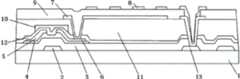
如图1所示,为现有的ADS模式下的TFT阵列基板结构,其中,最底层为基板1,然后至基板1向上依次为栅极2、绝缘层3、有源层4,在有源层4上方形成有漏极5和源极6,在光线传播的方向上,该漏极5和源极6的相关区域构成像素区域中的薄膜晶体管区域,而与之相对应的用作显示的区域部分形成有像素电极7(可视为板状电极)与漏极6相接触,在漏极5、源极6及像素电极7上覆盖有钝化层9,在钝化层9上沉积公共电极8(可视为狭缝电极),由此在光线传播的方向上,像素电极7与公共电极8的相关区域则构成了像素电极图形区域(也可以称之为显示区域)。该结构为一般的液晶显示装置,除了TFT-LCD阵列基板之外,还设有彩膜基板和背光源。通常情况下,TFT-LCD阵列基板和彩膜基板分开制备,然后通过对盒(Cell)工艺将阵列基板和彩膜基板对合在一起形成显示面板,最终通过模组(Moulde)工艺形成显示装置。为了降低成本,减少工艺步骤,各大厂商正逐渐采用将彩膜制备在阵列基板上的工艺(Color Filter On Array,COA)。As shown in Figure 1, it is the TFT array substrate structure under the existing ADS mode, wherein the bottom layer is the
但是,由于在目前的像素结构中,TFT区域厚度不同(图1中钝化层9在TFT处有明显凸起)影响了对盒后液晶分子填充的均匀度,液晶分子在反射区域存在不规则排列的情况;且由于像素结构内部像素电极距离数据线较近,受数据线电压的影响,像素区域在各层之间存在段差,这样的构造并不利于ADS模式的水平驱动,非常容易因非正常性的液晶驱动(Disclination)使得液晶分子偏转角度不足而导致漏光,由于漏光使得背光源发出的光未能在显示区域得到充分利用,从而导致面板的对比度过低,影响正常使用。However, in the current pixel structure, the thickness of the TFT area is different (the
发明内容Contents of the invention
(一)要解决的技术问题(1) Technical problems to be solved
本发明要解决的技术问题是如何提高液晶面板对比度的问题。The technical problem to be solved by the invention is how to improve the contrast of the liquid crystal panel.
(二)技术方案(2) Technical solution
为解决上述问题,本发明提供一种阵列基板,包括限定了像素区域的栅线和数据线,所述像素区域包括薄膜晶体管区域以及像素电极图形区域,所述薄膜晶体管区域中形成有栅极、栅绝缘层、有源层、源极、漏极以及钝化层;所述像素电极图形区域中形成所述栅绝缘层、像素电极、所述钝化层以及公共电极,其中,所述公共电极和像素电极构成了多维电场;在所述栅绝缘层与像素电极之间形成有彩色树脂层。In order to solve the above problems, the present invention provides an array substrate, including gate lines and data lines that define a pixel area, the pixel area includes a thin film transistor area and a pixel electrode pattern area, and the thin film transistor area is formed with a gate, A gate insulating layer, an active layer, a source electrode, a drain electrode, and a passivation layer; the gate insulating layer, the pixel electrode, the passivation layer, and a common electrode are formed in the pattern region of the pixel electrode, wherein the common electrode The multi-dimensional electric field is formed with the pixel electrode; a colored resin layer is formed between the gate insulating layer and the pixel electrode.
其中,在基板上像素电极图形区域对应的位置处设置有以栅金属材料形成的反射区域图案,所述栅绝缘层形成于所述反射区域图案上;在所述栅绝缘层上对应所述反射区域图案的位置处设置有以源/漏金属材料形成的反射区域金属电极层。Wherein, a reflective area pattern formed of a gate metal material is provided at a position corresponding to the pixel electrode pattern area on the substrate, and the gate insulating layer is formed on the reflective area pattern; corresponding to the reflective area pattern on the gate insulating layer A reflective regional metal electrode layer formed of source/drain metal material is arranged at the position of the regional pattern.
其中,在所述像素电极图形区域内还设置有以栅金属材料形成的存贮电容底电极,所述存贮电容底电极上方形成有绝缘层过孔,所述公共电极通过所述绝缘层过孔与存贮电容底电极相连。Wherein, a storage capacitor bottom electrode formed of a gate metal material is also provided in the pixel electrode pattern area, an insulating layer via hole is formed above the storage capacitor bottom electrode, and the common electrode passes through the insulating layer. The hole is connected to the bottom electrode of the storage capacitor.
其中,在源极、漏极以及栅绝缘层的上方还形成有绝缘材料的保护层,在所述保护层上对应薄膜晶体管区域的位置形成黑矩阵层。Wherein, a protective layer of insulating material is formed above the source electrode, the drain electrode and the gate insulating layer, and a black matrix layer is formed on the protective layer at a position corresponding to the thin film transistor region.
此外,本发明还提供一种阵列基板的制造方法,包括形成像素区域的过程,所述像素区域包括薄膜晶体管区域以及像素电极图形区域,在所述薄膜晶体管区域中形成栅极、栅绝缘层、有源层、源极、漏极以及钝化层;在所述像素电极图形区域中形成所述栅绝缘层、像素电极、所述钝化层以及公共电极,所述公共电极和像素电极构成了多维电场;其中,在形成栅绝缘层之后、形成像素电极之前,在栅绝缘层上方形成彩色树脂层。In addition, the present invention also provides a method for manufacturing an array substrate, including the process of forming a pixel area, the pixel area includes a thin film transistor area and a pixel electrode pattern area, forming a gate, a gate insulating layer, Active layer, source electrode, drain electrode and passivation layer; Form the gate insulating layer, pixel electrode, the passivation layer and common electrode in the pattern region of the pixel electrode, the common electrode and the pixel electrode constitute A multi-dimensional electric field; wherein, after forming the gate insulating layer and before forming the pixel electrodes, a colored resin layer is formed on the gate insulating layer.
其中,在形成栅极的过程中,还在基板上像素电极图形区域对应的位置处设置以栅金属材料形成的反射区域图案;在形成源极、漏极的过程中,还在所述栅绝缘层上对应所述反射区域图案的位置处设置以源/漏金属材料形成的反射区域金属电极层。Wherein, in the process of forming the gate, a reflective area pattern formed of a gate metal material is also provided at the position corresponding to the pixel electrode pattern area on the substrate; in the process of forming the source and drain, the gate insulation A reflective region metal electrode layer formed of source/drain metal material is arranged on the layer at a position corresponding to the reflective region pattern.
其中,在形成栅极的过程中,还在所述像素电极图形区域内设置以栅金属材料形成的存贮电容底电极;在形成像素电极之前,先在所述存贮电容底电极上方形成绝缘层过孔,以使在形成像素电极之后,所述公共电极通过所述绝缘层过孔与存贮电容底电极相连。Wherein, in the process of forming the gate, a storage capacitor bottom electrode formed of a gate metal material is also provided in the pixel electrode pattern area; before forming the pixel electrode, an insulating layer is formed above the storage capacitor bottom electrode. A layer via hole is provided so that after the pixel electrode is formed, the common electrode is connected to the bottom electrode of the storage capacitor through the insulating layer via hole.
其中,在形成了源极、漏极之后的基板上,形成绝缘材料的保护层,然后在所述保护层上对应薄膜晶体管区域的位置形成黑矩阵层。Wherein, a protective layer of insulating material is formed on the substrate after the source electrode and the drain electrode are formed, and then a black matrix layer is formed on the protective layer at a position corresponding to the thin film transistor region.
此外,本发明还提供一种包括所述阵列基板的显示装置。In addition, the present invention also provides a display device comprising the array substrate.
(三)有益效果(3) Beneficial effects
本发明技术方案对比现有技术,存在如下几点特征:Compared with the prior art, the technical solution of the present invention has the following characteristics:
(1)由于在薄膜晶体管的栅绝缘层上方形成彩色树脂层,增大了像素电极与数据线、栅线间的距离(即增大了层间厚度),这有利于使像素区域内部的结构平坦化,避免像素电极受数据线、栅线电压的影响,可以防止液晶在反射区域的不规则排列,有利于水平驱动的ADS模式,保证了液晶分子的适度偏转,可以防止漏光并提高对比度。(1) Since the color resin layer is formed above the gate insulating layer of the thin film transistor, the distance between the pixel electrode and the data line and the gate line is increased (that is, the interlayer thickness is increased), which is beneficial to make the structure inside the pixel area Planarization avoids the pixel electrode being affected by the voltage of the data line and the gate line, prevents the irregular arrangement of the liquid crystal in the reflective area, is conducive to the ADS mode of the horizontal drive, ensures the moderate deflection of the liquid crystal molecules, prevents light leakage and improves the contrast.
(2)进一步地,通过采用栅极金属材料形成反射区域的图案,采用源、漏极金属材料形成反射区域金属电极层,且彩色树脂层制备在反射区域金属电极层之上,同样增大了像素电极与反射区域电极间的距离,这样也可以避免液晶分子在反射区域的不规则排列所导致的漏光;此外,反射区域的设置(即半透半反方式)使得液晶面板可以利用外界光线增强在强光下的显示,提高产品品质,并且可以节约材料投入,降低制造成本。(2) Further, by using the grid metal material to form the pattern of the reflective area, using the source and drain metal materials to form the metal electrode layer in the reflective area, and the colored resin layer is prepared on the metal electrode layer in the reflective area, which also increases the The distance between the pixel electrode and the reflective area electrode can also avoid light leakage caused by the irregular arrangement of liquid crystal molecules in the reflective area; in addition, the setting of the reflective area (that is, the transflective mode) enables the liquid crystal panel to use external light to enhance The display under strong light improves product quality, saves material input and reduces manufacturing costs.
(3)更进一步地,由于无需将阵列基板与另外的彩膜基板进行对盒,直接将液晶填充在阵列基板与一层玻璃基板之间即可,减少了对盒控制,同时由于公共电极通过绝缘层过孔与存贮电容底电极相连,形成高开口率的结构,可以有效提高透过率。(3) Furthermore, since there is no need to align the array substrate with another color filter substrate, it is sufficient to directly fill the liquid crystal between the array substrate and a layer of glass substrate, which reduces the control of the array substrate, and at the same time, because the common electrode passes through The via hole in the insulating layer is connected to the bottom electrode of the storage capacitor to form a structure with a high aperture ratio, which can effectively improve the transmittance.
附图说明Description of drawings
图1为现有技术中ADS模式下阵列基板的侧视示意图;1 is a schematic side view of an array substrate in ADS mode in the prior art;
图2为本发明实施例1的阵列基板的侧视示意图;2 is a schematic side view of an array substrate according to
图3a及图3b为本发明实施例1的阵列基板的制作流程图;3a and 3b are the flow charts of manufacturing the array substrate according to
图4为本发明实施例2在阵列基板的侧视示意图;4 is a schematic side view of an array substrate in
其中,1:基板、2:栅极、3:栅绝缘层、4:有源层、5:源极、6:漏极、7:像素电极、8:公共电极、9:钝化层、10:黑矩阵层、11:彩色树脂层、12:保护层、13:存贮电容底电极、14:反射区域图案、15:反射区域金属电极层。Among them, 1: Substrate, 2: Gate, 3: Gate insulating layer, 4: Active layer, 5: Source, 6: Drain, 7: Pixel electrode, 8: Common electrode, 9: Passivation layer, 10 : black matrix layer, 11: color resin layer, 12: protective layer, 13: storage capacitor bottom electrode, 14: reflective area pattern, 15: reflective area metal electrode layer.
具体实施方式Detailed ways
为使本发明的目的、内容、和优点更加清楚,下面结合附图和实施例,对本发明的具体实施方式作进一步详细描述。In order to make the purpose, content, and advantages of the present invention clearer, the specific implementation manners of the present invention will be further described in detail below in conjunction with the accompanying drawings and embodiments.
实施例1Example 1
本实施例具体提供一种阵列基板,其可以应用于ADS驱动模式下,如图2所示,其包括限定了像素区域的栅线和数据线,所述像素区域包括薄膜晶体管区域以及像素电极图形区域,所述薄膜晶体管区域中形成有栅极2、栅绝缘层3、有源层4、源极5、漏极6以及钝化层9;所述像素电极图形区域中形成所述栅绝缘层3、像素电极7、所述钝化层9以及公共电极8,其中,所述公共电极8和像素电极7构成了多维电场;在所述栅绝缘层3和源极/漏极上方可以选择覆盖保护层12然后在源极/漏极和TFT沟道上方形成黑矩阵层10,或者无需覆盖保护层12而直接在源极/漏极和TFT沟道上方形成黑矩阵层10。This embodiment specifically provides an array substrate, which can be applied in the ADS driving mode, as shown in FIG. 2 , which includes gate lines and data lines defining a pixel area, and the pixel area includes a thin film transistor area and a pixel electrode pattern In the region of the thin film transistor, a
当选择覆盖保护层12时,在所述保护层12上对应薄膜晶体管的位置处形成黑矩阵层10,在所述保护层12及黑矩阵层10所形成的表面与像素电极7之间形成有彩色树脂层11;当选择直接在栅绝缘层3上对应薄膜晶体管的位置处形成黑矩阵层10时,则在所述栅绝缘层3及黑矩阵层10所形成的表面与像素电极7之间形成彩色树脂层11。所述保护层12的形成有利于像素区域内部的结构更加平坦化。When the
其中,在所述像素电极图形区域内还设置有以栅金属材料形成的存贮电容底电极13,所述存贮电容底电极13上方形成有绝缘层过孔,该绝缘层过孔贯穿钝化层9、彩色树脂层11、保护层12和栅绝缘层3,所述公共电极8通过所述绝缘层过孔与存贮电容底电极13相连。Wherein, a storage
在本实施例中,上述存贮电容底电极13可以是为公共电极8提供恒定电压的公共电极线(Cst on common),也可以是栅线的一部分(Cst on Gate)。In this embodiment, the storage
此外,本实施例还提供一种阵列基板的制造方法,如图3a及图3b所示,该工艺可以概括为首先形成包括栅线、栅极2、栅绝缘层3、有源层4、源极5、漏极6、数据线的图形,从而构成出薄膜晶体管区域;然后形成包括彩色树脂层11的图形;最后形成包括像素电极7、钝化层9、公共电极8的图形,构成像素电极图形区域。其具备如下步骤:In addition, this embodiment also provides a method for manufacturing an array substrate. As shown in FIG. 3a and FIG.
步骤S1:首先在基板1上形成包括栅线、栅极2、栅绝缘层3、有源层4、源极5、漏极6、数据线的图形,从而构成出薄膜晶体管区域,然后在所形成的基板上形成绝缘材料的保护层12;该步骤对应于步骤S101、S102及S103,具体为:Step S1: Firstly, a pattern including gate line,
步骤S101:在基板1上沉积导电性好的第一金属层,利用第一掩膜工艺刻蚀出栅线、栅极2及像素电极图形区域内的存贮电容底电极13;Step S101: Deposit a first metal layer with good conductivity on the
步骤S102:在所形成的基板上依次沉积采用SiNx或SiON等材料的栅绝缘层3、采用a-Si等材料的半导体有源层4;在所形成的基板上沉积导电性好的第二金属层,利用半色调掩膜(Halftone Mask)的第二掩膜工艺描绘出源极5、漏极6以及薄膜晶体管沟道部的图案,然后利用连续刻蚀工艺和灰化工艺刻蚀出源极5、漏极6,从而构成薄膜晶体管区域;并刻蚀掉包含上述沟道部不纯物质的半导体层;Step S102: sequentially depositing a
步骤S103:为了保护上述基板的薄膜晶体管部分以及像素部分,在所形成的基板上形成SiNx等绝缘材料的保护层12;Step S103: In order to protect the thin film transistor part and the pixel part of the above-mentioned substrate, a
步骤S2:在步骤S1形成的基板上方沉积不透明树脂层,并利用第三掩膜工艺在薄膜晶体管区域对应的位置上刻蚀出黑矩阵层10;Step S2: Depositing an opaque resin layer on the substrate formed in step S1, and etching a
步骤S3:形成包括彩色树脂层11的图形;该步骤对应步骤S301及S302,具体为:Step S3: forming a pattern including the colored
步骤S301:在步骤2形成的基板上首先沉积R(Red,红色)树脂层,同时利用第四掩膜工艺进行刻蚀,再在刻蚀完成的基板上以与R树脂层相似的方式来沉积并利用第五、第六刻蚀工艺来刻蚀G(Green,绿色)树脂层以及B(Blue,蓝色)树脂层,从而形成出彩色树脂层11,最后,刻蚀掉存贮电容底电极13上方的彩色树脂层11,使存贮电容底电极13暴露出来;Step S301: first deposit an R (Red, red) resin layer on the substrate formed in
步骤S302:利用第七掩膜工艺刻蚀掉存贮电容底电极13上方的栅绝缘层3及保护层12,使存贮电容底电极13暴露出来,形成开口朝上的绝缘层过孔;Step S302: using the seventh mask process to etch away the
在接下来的步骤S4及S5中将形成包括像素电极7、钝化层9、公共电极8的图形,具体为:In the following steps S4 and S5, a pattern comprising the
步骤S4:在步骤S3形成的基板上沉积第一透明导电层,利用第八掩膜工艺刻蚀出像素电极7;Step S4: depositing a first transparent conductive layer on the substrate formed in step S3, and etching the
步骤S5:形成钝化层9及公共电极8,其中,公共电极8通过上述步骤S302中形成的绝缘层过孔与存贮电容底电极13相连;其对应于步骤S501及S502,具体为:Step S5: forming a
步骤S501:在步骤S4形成的基板上沉积透明树脂材料层,并利用第九掩膜工艺刻蚀出钝化层9;Step S501: depositing a transparent resin material layer on the substrate formed in step S4, and etching the
步骤S502:在步骤S501形成的基板上沉积第二透明导电层,利用第十掩膜工艺刻蚀出公共电极8。Step S502: depositing a second transparent conductive layer on the substrate formed in step S501, and etching the
其中,所述不透明树脂层所采用的材料优选为面电阻大于1012Ω/sq,厚度为0.5μm~2μm,光密度(Optical density,OP)为4以上的材料。Wherein, the material used for the opaque resin layer is preferably a material with a surface resistance greater than 1012 Ω/sq, a thickness of 0.5 μm-2 μm, and an optical density (Optical density, OP) of 4 or more.
其中,所述RGB树脂层的材料,优选为其介电常数范围为3~5F/m,厚度为1μm~4μm。Wherein, the material of the RGB resin layer preferably has a dielectric constant in the range of 3-5 F/m and a thickness of 1 μm-4 μm.
其中,所述第一透明导电层及第二透明导电层所采用的材料优选为可与布线金属(比如Mo、AI、Ti、Cu等导电性好的金属或其合金)进行选择性湿法刻蚀(Wet Etch)的材料,比如ITO(Indium Tin Oxide,纳米铟锡金属氧化物),IZO(Indium Zinc Oxide,氧化铟锌)等,这样的材料经过TCO(Transparent Conducting Oxide,透明引导氧化)处理成为透明性良好的材料。Wherein, the materials used in the first transparent conductive layer and the second transparent conductive layer are preferably capable of selective wet etching with wiring metals (such as Mo, Al, Ti, Cu and other metals with good conductivity or their alloys). Wet Etch materials, such as ITO (Indium Tin Oxide, nano-indium tin metal oxide), IZO (Indium Zinc Oxide, indium zinc oxide), etc., such materials are treated by TCO (Transparent Conducting Oxide, transparent guided oxidation) It becomes a material with good transparency.
其中,所述构成钝化层9的透明树脂材料层材料优选为树脂介电常数在3~5F/m之间,厚度为1μm~4μm的材料。Wherein, the material of the transparent resin material layer constituting the
实施例2Example 2
本实施例提供另一种阵列基板,鉴于上述实施例1已给出了详细说明,因此某些重复的内容将在本实施例中给予省略,在此仅主要对区别之处进行详细说明。This embodiment provides another array substrate. Since the above-mentioned
本实施例所提供的阵列基板,其可以应用于ADS驱动模式下,如图4所示,其包括限定了像素区域的栅线和数据线,所述像素区域包括薄膜晶体管区域以及像素电极图形区域,所述薄膜晶体管区域中形成有栅极2、栅绝缘层3、有源层4、源极5、漏极6以及钝化层9;所述像素电极图形区域中形成所述栅绝缘层3、像素电极7、所述钝化层9以及公共电极8,其中,所述公共电极8和像素电极7构成了多维电场。The array substrate provided by this embodiment can be applied in the ADS driving mode, as shown in FIG. 4 , it includes gate lines and data lines defining a pixel area, and the pixel area includes a thin film transistor area and a pixel electrode pattern area , the
其中,在基板1上像素电极图形区域对应的位置处设置有以栅金属材料形成的反射区域图案14,所述栅绝缘层3形成于所述反射区域图案14上。在所述栅绝缘层3上对应所述反射区域图案14的位置处设置有以源/漏金属材料形成的反射区域金属电极层15。由此,形成了一种半透半反式的阵列基板结构,可以适用于在户外等强光环境下的阅读显示。Wherein, a
关于该阵列基板的制造方法,说明如下:The manufacturing method of the array substrate is described as follows:
该方法具体包括:The method specifically includes:
步骤1:利用第一金属材料来制备栅线、栅极2及存贮电容底电极(未图示),并在像素电极图形区域对应的位置保留部分栅金属材料的图案,从而利用栅金属形成一些凹凸图案,用来形成反射区域图案14,所使用的第一金属材料优选为Al、AlNd、Mo等;Step 1: Use the first metal material to prepare the gate line, the
在本实施例中,上述存贮电容底电极可以是为公共电极提供恒定电压的公共电极线(Cst on common),也可以是栅线的一部分(Cst onGate)。In this embodiment, the bottom electrode of the above-mentioned storage capacitor may be a common electrode line (Cs on common ) that provides a constant voltage for the common electrode, or may be a part of the gate line (Cs on Gate).
步骤2:形成栅绝缘层3,并利用半导体材料制备半导体硅岛层,形成有源层4,材料优选为a-si、p-Si、IGZO等;Step 2: forming a
步骤3:利用第二金属材料来制备数据线和源极5、漏极6,并在栅金属凹凸的反射区域图案14对应的栅绝缘层3上部保留部分源、漏极金属材料,形成反射区域金属电极层15,用来实现金属反射层的功能,第二金属材料优选为Al、AlNd、Mo等;Step 3: Use the second metal material to prepare the data line and the
步骤4~6:首先沉积R树脂层,同时利用掩膜工艺进行刻蚀,再在刻蚀完成的基板上以与R树脂层相似的方式来沉积并刻蚀G树脂层以及B树脂层,从而形成出彩色树脂层11;Steps 4-6: first deposit the R resin layer, and at the same time use a mask process to etch, and then deposit and etch the G resin layer and the B resin layer on the etched substrate in a similar manner to the R resin layer, so that forming a
步骤7:利用透明导电材料来制备与漏极6相连的像素电极7,透明导电材料优选为ITO、IZO等;Step 7: using a transparent conductive material to prepare the
步骤8:通过无机绝缘材料来制备钝化层9,无机绝缘材料优选为SiNx、SiOx等;Step 8: Prepare the
步骤9:利用透明导电材料来制备公共电极8,公共电极8通过过孔与所述存贮电容底电极相连(未图示),透明导电材料优选为ITO、IZO等;Step 9: using a transparent conductive material to prepare the
进一步地,之后在所形成的基板的薄膜晶体管区域可以再利用不透明树脂层来形成黑矩阵层。Further, the opaque resin layer can be used to form a black matrix layer in the thin film transistor region of the formed substrate afterwards.
本领域技术人员应该可以理解,像素电极可以为板状或者狭缝状,公共电极也是如此,像素电极和公共电极的上下顺序可颠倒,但是在上的电极必须是狭缝状的,在下的电极是板状的。Those skilled in the art should understand that the pixel electrodes can be plate-shaped or slit-shaped, and the same is true for the common electrodes. It is plank.
同时,本发明还提供一种显示装置,所述显示装置包括上述实施例中任一种的阵列基板,所述显示装置可以为:液晶面板、电子纸、OLED面板、液晶电视、液晶显示器、数码相框、手机、平板电脑等具有任何显示功能的产品或部件。At the same time, the present invention also provides a display device, which includes the array substrate of any one of the above embodiments, and the display device can be: a liquid crystal panel, an electronic paper, an OLED panel, a liquid crystal TV, a liquid crystal display, a digital display, etc. Products or components with any display function, such as photo frames, mobile phones, tablets, etc.
以上所述仅是本发明的优选实施方式,应当指出,对于本技术领域的普通技术人员来说,在不脱离本发明技术原理的前提下,还可以做出若干改进和变形,这些改进和变形也应视为本发明的保护范围。The above is only a preferred embodiment of the present invention, it should be pointed out that for those of ordinary skill in the art, without departing from the technical principle of the present invention, some improvements and modifications can also be made. It should also be regarded as the protection scope of the present invention.
Claims (7)
Priority Applications (6)
| Application Number | Priority Date | Filing Date | Title |
|---|---|---|---|
| CN201210048847.8ACN102681276B (en) | 2012-02-28 | 2012-02-28 | Array substrate, method for manufacturing same and display device comprising same |
| PCT/CN2012/087234WO2013127236A1 (en) | 2012-02-28 | 2012-12-23 | Array substrate, manufacturing method therefor and display device |
| KR1020137008359AKR20130108574A (en) | 2012-02-28 | 2012-12-23 | Array substrate, manufacturing method thereof, and display device |
| EP12837626.6AEP2660651B1 (en) | 2012-02-28 | 2012-12-23 | Array substrate, manufacturing method therefor and display device |
| JP2014557978AJP2015511026A (en) | 2012-02-28 | 2012-12-23 | Array substrate, method for manufacturing the same, and display device |
| US13/878,475US20140054581A1 (en) | 2012-02-28 | 2012-12-23 | Array substrate, manufacturing method thereof, and display device |
Applications Claiming Priority (1)
| Application Number | Priority Date | Filing Date | Title |
|---|---|---|---|
| CN201210048847.8ACN102681276B (en) | 2012-02-28 | 2012-02-28 | Array substrate, method for manufacturing same and display device comprising same |
Publications (2)
| Publication Number | Publication Date |
|---|---|
| CN102681276A CN102681276A (en) | 2012-09-19 |
| CN102681276Btrue CN102681276B (en) | 2014-07-09 |
Family
ID=46813420
Family Applications (1)
| Application Number | Title | Priority Date | Filing Date |
|---|---|---|---|
| CN201210048847.8AActiveCN102681276B (en) | 2012-02-28 | 2012-02-28 | Array substrate, method for manufacturing same and display device comprising same |
Country Status (6)
| Country | Link |
|---|---|
| US (1) | US20140054581A1 (en) |
| EP (1) | EP2660651B1 (en) |
| JP (1) | JP2015511026A (en) |
| KR (1) | KR20130108574A (en) |
| CN (1) | CN102681276B (en) |
| WO (1) | WO2013127236A1 (en) |
Families Citing this family (48)
| Publication number | Priority date | Publication date | Assignee | Title |
|---|---|---|---|---|
| CN202404339U (en)* | 2012-01-12 | 2012-08-29 | 京东方科技集团股份有限公司 | Array substrate and display device comprising same |
| CN102681276B (en)* | 2012-02-28 | 2014-07-09 | 京东方科技集团股份有限公司 | Array substrate, method for manufacturing same and display device comprising same |
| TWI547477B (en) | 2012-03-14 | 2016-09-01 | 大賽璐股份有限公司 | Process for producing acetic acid |
| CN102854685A (en)* | 2012-09-26 | 2013-01-02 | 南京中电熊猫液晶显示科技有限公司 | Metallic oxide fringing field switching mode liquid crystal display panel and manufacture method thereof |
| CN102931139B (en)* | 2012-11-05 | 2015-07-01 | 京东方科技集团股份有限公司 | Array substrate and manufacture method and display device thereof |
| CN102998867B (en)* | 2012-11-20 | 2015-06-03 | 京东方科技集团股份有限公司 | Array substrate, display panel, manufacturing method and display device |
| CN103018991B (en) | 2012-12-24 | 2015-01-28 | 京东方科技集团股份有限公司 | Array substrate, manufacturing method thereof and display device |
| CN103117284A (en) | 2013-02-01 | 2013-05-22 | 京东方科技集团股份有限公司 | Array substrate and manufacturing method thereof and display device |
| CN103309095B (en) | 2013-05-30 | 2015-08-26 | 京东方科技集团股份有限公司 | A kind of array base palte and preparation method thereof, display device |
| CN103309081B (en)* | 2013-05-30 | 2016-12-28 | 京东方科技集团股份有限公司 | Array base palte and manufacture method, display device |
| CN103309106B (en)* | 2013-07-10 | 2015-11-11 | 深圳市华星光电技术有限公司 | Colorful filter array substrate and manufacture method thereof |
| JP6188473B2 (en)* | 2013-07-31 | 2017-08-30 | 三菱電機株式会社 | Thin film transistor array substrate and manufacturing method thereof |
| CN103487982A (en) | 2013-08-19 | 2014-01-01 | 京东方科技集团股份有限公司 | Display device, array substrate, pixel structure and manufacturing method |
| CN103472646B (en)* | 2013-08-30 | 2016-08-31 | 京东方科技集团股份有限公司 | A kind of array base palte and preparation method thereof and display device |
| CN103456764B (en)* | 2013-09-09 | 2016-01-20 | 京东方科技集团股份有限公司 | OLED array and manufacture method, display unit |
| CN103489826B (en)* | 2013-09-26 | 2015-08-05 | 京东方科技集团股份有限公司 | Array base palte, preparation method and display unit |
| TWI642170B (en)* | 2013-10-18 | 2018-11-21 | 半導體能源研究所股份有限公司 | Display device and electronic device |
| CN103700669A (en)* | 2013-12-19 | 2014-04-02 | 京东方科技集团股份有限公司 | Array substrate and preparation method thereof as well as display device |
| CN103715204B (en)* | 2013-12-27 | 2015-05-27 | 京东方科技集团股份有限公司 | Array substrate, manufacturing method thereof, and display device |
| CN103928472A (en)* | 2014-03-26 | 2014-07-16 | 京东方科技集团股份有限公司 | Array substrate, manufacturing method thereof, and display device |
| CN104090434B (en)* | 2014-06-25 | 2016-10-05 | 京东方科技集团股份有限公司 | Array base palte and display device |
| CN104216186B (en)* | 2014-08-15 | 2018-01-26 | 京东方科技集团股份有限公司 | Array substrate, manufacturing method thereof, and display device |
| CN104332473A (en)* | 2014-08-29 | 2015-02-04 | 京东方科技集团股份有限公司 | Array substrate and preparation method thereof, display panel and display device |
| CN104317097A (en)* | 2014-10-31 | 2015-01-28 | 京东方科技集团股份有限公司 | COA (color filter on array) substrate, production method thereof and display device |
| CN104298040B (en)* | 2014-10-31 | 2018-07-06 | 京东方科技集团股份有限公司 | A kind of COA substrates and preparation method thereof and display device |
| CN104375344B (en)* | 2014-11-21 | 2017-09-15 | 深圳市华星光电技术有限公司 | Liquid crystal display panel and its color membrane array substrate |
| CN104536213A (en)* | 2014-12-19 | 2015-04-22 | 深圳市华星光电技术有限公司 | FFS array substrate and liquid crystal display panel |
| CN104536194A (en)* | 2015-01-04 | 2015-04-22 | 京东方科技集团股份有限公司 | Array substrate, method for manufacturing array substrate and display device |
| CN105842929B (en)* | 2015-01-12 | 2020-12-29 | 群创光电股份有限公司 | display device |
| TWI557488B (en)* | 2015-01-12 | 2016-11-11 | 群創光電股份有限公司 | Display |
| CN104617039A (en)* | 2015-01-27 | 2015-05-13 | 京东方科技集团股份有限公司 | Array substrate, and manufacture method and display device thereof |
| CN104617109B (en)* | 2015-01-28 | 2018-04-20 | 昆山龙腾光电有限公司 | Thin-film transistor array base-plate and preparation method thereof, liquid crystal display device |
| CN105990231B (en)* | 2015-02-25 | 2019-10-18 | 南京瀚宇彩欣科技有限责任公司 | Manufacturing method of thin film transistor substrate |
| CN104733456B (en) | 2015-03-23 | 2018-04-27 | 京东方科技集团股份有限公司 | A kind of array base palte and preparation method thereof, display device |
| CN104765191B (en)* | 2015-04-30 | 2018-07-06 | 京东方科技集团股份有限公司 | Array substrate and preparation method thereof and display device |
| CN104808408B (en)* | 2015-05-15 | 2018-09-07 | 合肥鑫晟光电科技有限公司 | A kind of production method of COA substrates, display device and COA substrates |
| CN104880847B (en)* | 2015-06-18 | 2019-04-30 | 深圳市华星光电技术有限公司 | IPS type On Cell touch-control display panel and preparation method thereof |
| CN104934449B (en)* | 2015-07-16 | 2017-12-05 | 京东方科技集团股份有限公司 | Display base plate and preparation method thereof and display device |
| KR102148491B1 (en) | 2015-12-14 | 2020-08-26 | 엘지디스플레이 주식회사 | Thin film transistor substrate |
| JP6651859B2 (en)* | 2016-01-12 | 2020-02-19 | 凸版印刷株式会社 | Thin film transistor array and reflective display device |
| CN105511177A (en)* | 2016-02-02 | 2016-04-20 | 京东方科技集团股份有限公司 | Array substrate and liquid crystal display device |
| CN106024810A (en)* | 2016-07-13 | 2016-10-12 | 京东方科技集团股份有限公司 | Flexible display substrate and manufacturing method thereof and display device |
| CN111446260B (en)* | 2020-03-31 | 2023-07-21 | 京东方科技集团股份有限公司 | Array substrate, manufacturing method thereof, and display device |
| CN111694464B (en)* | 2020-06-19 | 2024-04-19 | 京东方科技集团股份有限公司 | Array substrate, preparation method thereof and display device |
| US11650705B2 (en)* | 2020-12-07 | 2023-05-16 | Tpk Advanced Solutions Inc. | Touch panel, electronic device and manufacture method thereof |
| JP7625911B2 (en)* | 2021-03-12 | 2025-02-04 | セイコーエプソン株式会社 | Electro-optical devices and electronic equipment |
| CN114089570B (en)* | 2021-11-22 | 2023-11-10 | 京东方科技集团股份有限公司 | Array substrate and preparation method thereof, display panel and display device |
| CN117476672B (en)* | 2022-12-30 | 2025-09-19 | 广州华星光电半导体显示技术有限公司 | Array substrate and preparation method thereof |
Citations (3)
| Publication number | Priority date | Publication date | Assignee | Title |
|---|---|---|---|---|
| CN1369731A (en)* | 2001-01-29 | 2002-09-18 | 株式会社日立制作所 | Liquid crystal display device |
| CN101750821A (en)* | 2008-12-03 | 2010-06-23 | 株式会社半导体能源研究所 | Liquid crystal display device with a light guide plate |
| CN102227678A (en)* | 2008-11-28 | 2011-10-26 | 夏普株式会社 | Liquid crystal display device and method for manufacturing TFT substrate of liquid crystal display device |
Family Cites Families (15)
| Publication number | Priority date | Publication date | Assignee | Title |
|---|---|---|---|---|
| JP2001066617A (en)* | 1999-08-27 | 2001-03-16 | Nec Corp | Liquid crystal display device and its production |
| JP3750055B2 (en)* | 2001-02-28 | 2006-03-01 | 株式会社日立製作所 | Liquid crystal display |
| KR100945442B1 (en)* | 2003-02-28 | 2010-03-05 | 엘지디스플레이 주식회사 | CIO structure transflective liquid crystal display |
| TWI261716B (en)* | 2004-05-13 | 2006-09-11 | Quanta Display Inc | Liquid crystal display apparatus and fabrication thereof |
| EP1793266B1 (en)* | 2005-12-05 | 2017-03-08 | Semiconductor Energy Laboratory Co., Ltd. | Transflective Liquid Crystal Display with a Horizontal Electric Field Configuration |
| JP2007178810A (en)* | 2005-12-28 | 2007-07-12 | Lg Philips Lcd Co Ltd | Liquid crystal display |
| TWI545380B (en)* | 2006-05-16 | 2016-08-11 | 半導體能源研究所股份有限公司 | Liquid crystal display device and semiconductor device |
| EP2053452A3 (en)* | 2006-08-02 | 2012-03-14 | Sharp Kabushiki Kaisha | Display device |
| JP4487318B2 (en)* | 2007-07-26 | 2010-06-23 | エプソンイメージングデバイス株式会社 | Liquid crystal display device and manufacturing method thereof |
| JP2009139853A (en)* | 2007-12-10 | 2009-06-25 | Sharp Corp | Liquid crystal display device |
| KR101423113B1 (en)* | 2007-12-18 | 2014-07-25 | 삼성디스플레이 주식회사 | Thin film transistor display panel and manufacturing method thereof |
| KR101330330B1 (en)* | 2008-12-30 | 2013-11-15 | 엘지디스플레이 주식회사 | In-Plane Switching mode Liquid crystal display device |
| CN101968590B (en)* | 2010-10-27 | 2014-07-02 | 友达光电股份有限公司 | Liquid crystal display panel |
| CN202084547U (en)* | 2011-06-02 | 2011-12-21 | 北京京东方光电科技有限公司 | Array substrate, liquid crystal plane and display equipment |
| CN102681276B (en)* | 2012-02-28 | 2014-07-09 | 京东方科技集团股份有限公司 | Array substrate, method for manufacturing same and display device comprising same |
- 2012
- 2012-02-28CNCN201210048847.8Apatent/CN102681276B/enactiveActive
- 2012-12-23WOPCT/CN2012/087234patent/WO2013127236A1/enactiveApplication Filing
- 2012-12-23KRKR1020137008359Apatent/KR20130108574A/ennot_activeCeased
- 2012-12-23EPEP12837626.6Apatent/EP2660651B1/enactiveActive
- 2012-12-23USUS13/878,475patent/US20140054581A1/ennot_activeAbandoned
- 2012-12-23JPJP2014557978Apatent/JP2015511026A/enactivePending
Patent Citations (3)
| Publication number | Priority date | Publication date | Assignee | Title |
|---|---|---|---|---|
| CN1369731A (en)* | 2001-01-29 | 2002-09-18 | 株式会社日立制作所 | Liquid crystal display device |
| CN102227678A (en)* | 2008-11-28 | 2011-10-26 | 夏普株式会社 | Liquid crystal display device and method for manufacturing TFT substrate of liquid crystal display device |
| CN101750821A (en)* | 2008-12-03 | 2010-06-23 | 株式会社半导体能源研究所 | Liquid crystal display device with a light guide plate |
Also Published As
| Publication number | Publication date |
|---|---|
| CN102681276A (en) | 2012-09-19 |
| EP2660651B1 (en) | 2018-01-31 |
| EP2660651A1 (en) | 2013-11-06 |
| JP2015511026A (en) | 2015-04-13 |
| KR20130108574A (en) | 2013-10-04 |
| EP2660651A4 (en) | 2015-07-01 |
| US20140054581A1 (en) | 2014-02-27 |
| WO2013127236A1 (en) | 2013-09-06 |
Similar Documents
| Publication | Publication Date | Title |
|---|---|---|
| CN102681276B (en) | Array substrate, method for manufacturing same and display device comprising same | |
| KR101030545B1 (en) | LCD display device | |
| US10048553B2 (en) | BOA liquid crystal display panel and manufacturing method thereof | |
| JP4167085B2 (en) | Liquid crystal display | |
| CN102629606B (en) | Array substrate and preparation method thereof and display device | |
| US8933472B2 (en) | Array substrate and display device comprising the same | |
| KR102334140B1 (en) | Display device and manufacturing method thereof | |
| CN102929058B (en) | Array substrate, manufacturing method of array substrate, and display device | |
| EP2991121B1 (en) | Array substrate, method for manufacturing array substrate and display device | |
| US20170200750A1 (en) | Method for manufacturing array substrate | |
| CN104035231B (en) | Liquid crystal display panel and liquid crystal display device comprising same | |
| CN112578585B (en) | Display panel, manufacturing method thereof, and display device | |
| CN108490701A (en) | Display panel and its manufacturing method, display device | |
| CN103309100A (en) | Liquid crystal display device and method of fabricating the same | |
| US9110340B2 (en) | Array substrate, liquid crystal panel and liquid crystal display device comprising protrusion electrode parts | |
| CN105093756A (en) | Liquid crystal display pixel structure and manufacturing method thereof | |
| EP3614201A1 (en) | Array substrate structure and method for manufacturing array substrate | |
| CN105470266A (en) | FFS (fringe field switching) type array substrate and manufacturing method therefor | |
| US10928686B2 (en) | Array substrate, liquid crystal display panel and display device | |
| CN105679773A (en) | Array substrate and preparation method thereof | |
| CN102890373A (en) | In-plane switching liquid crystal display panel and method of manufacturing the same | |
| CN202533686U (en) | Array substrate and display equipment | |
| CN102854681A (en) | Array substrate, display device, and manufacture method of array substrate | |
| CN108388057B (en) | Array substrate | |
| CN113707668B (en) | Array substrate, preparation method thereof, liquid crystal panel and display device |
Legal Events
| Date | Code | Title | Description |
|---|---|---|---|
| C06 | Publication | ||
| PB01 | Publication | ||
| C10 | Entry into substantive examination | ||
| SE01 | Entry into force of request for substantive examination | ||
| C14 | Grant of patent or utility model | ||
| GR01 | Patent grant |