CN102668097A - Semiconductor device - Google Patents
Semiconductor deviceDownload PDFInfo
- Publication number
- CN102668097A CN102668097ACN2010800525457ACN201080052545ACN102668097ACN 102668097 ACN102668097 ACN 102668097ACN 2010800525457 ACN2010800525457 ACN 2010800525457ACN 201080052545 ACN201080052545 ACN 201080052545ACN 102668097 ACN102668097 ACN 102668097A
- Authority
- CN
- China
- Prior art keywords
- film
- oxide semiconductor
- insulating film
- electrode
- transistor
- Prior art date
- Legal status (The legal status is an assumption and is not a legal conclusion. Google has not performed a legal analysis and makes no representation as to the accuracy of the status listed.)
- Granted
Links
- 239000004065semiconductorSubstances0.000titleclaimsabstractdescription520
- 239000001257hydrogenSubstances0.000claimsabstractdescription131
- 229910052739hydrogenInorganic materials0.000claimsabstractdescription131
- UFHFLCQGNIYNRP-UHFFFAOYSA-NHydrogenChemical compound[H][H]UFHFLCQGNIYNRP-UHFFFAOYSA-N0.000claimsabstractdescription113
- 229910052751metalInorganic materials0.000claimsabstractdescription78
- 239000002184metalSubstances0.000claimsabstractdescription77
- 229910052782aluminiumInorganic materials0.000claimsabstractdescription74
- XAGFODPZIPBFFR-UHFFFAOYSA-NaluminiumChemical compound[Al]XAGFODPZIPBFFR-UHFFFAOYSA-N0.000claimsabstractdescription71
- 239000010936titaniumSubstances0.000claimsabstractdescription50
- RTAQQCXQSZGOHL-UHFFFAOYSA-NTitaniumChemical compound[Ti]RTAQQCXQSZGOHL-UHFFFAOYSA-N0.000claimsabstractdescription49
- 229910052719titaniumInorganic materials0.000claimsabstractdescription49
- 229910052721tungstenInorganic materials0.000claimsabstractdescription37
- 239000010937tungstenSubstances0.000claimsabstractdescription37
- ZOKXTWBITQBERF-UHFFFAOYSA-NMolybdenumChemical compound[Mo]ZOKXTWBITQBERF-UHFFFAOYSA-N0.000claimsabstractdescription35
- 229910052750molybdenumInorganic materials0.000claimsabstractdescription35
- 239000011733molybdenumSubstances0.000claimsabstractdescription35
- WFKWXMTUELFFGS-UHFFFAOYSA-NtungstenChemical compound[W]WFKWXMTUELFFGS-UHFFFAOYSA-N0.000claimsabstractdescription35
- 239000011777magnesiumSubstances0.000claimsabstractdescription20
- 229910052749magnesiumInorganic materials0.000claimsabstractdescription16
- FYYHWMGAXLPEAU-UHFFFAOYSA-NMagnesiumChemical compound[Mg]FYYHWMGAXLPEAU-UHFFFAOYSA-N0.000claimsabstractdescription14
- 229910052727yttriumInorganic materials0.000claimsabstractdescription14
- VWQVUPCCIRVNHF-UHFFFAOYSA-Nyttrium atomChemical compound[Y]VWQVUPCCIRVNHF-UHFFFAOYSA-N0.000claimsabstractdescription14
- XUIMIQQOPSSXEZ-UHFFFAOYSA-NSiliconChemical compound[Si]XUIMIQQOPSSXEZ-UHFFFAOYSA-N0.000claimsdescription50
- 229910052710siliconInorganic materials0.000claimsdescription50
- 239000010703siliconSubstances0.000claimsdescription50
- VYPSYNLAJGMNEJ-UHFFFAOYSA-NSilicium dioxideChemical compoundO=[Si]=OVYPSYNLAJGMNEJ-UHFFFAOYSA-N0.000claimsdescription46
- 229910052814silicon oxideInorganic materials0.000claimsdescription45
- 229910052581Si3N4Inorganic materials0.000claimsdescription30
- HQVNEWCFYHHQES-UHFFFAOYSA-Nsilicon nitrideChemical compoundN12[Si]34N5[Si]62N3[Si]51N64HQVNEWCFYHHQES-UHFFFAOYSA-N0.000claimsdescription29
- VYZAMTAEIAYCRO-UHFFFAOYSA-NChromiumChemical compound[Cr]VYZAMTAEIAYCRO-UHFFFAOYSA-N0.000claimsdescription20
- 229910052779NeodymiumInorganic materials0.000claimsdescription20
- QEFYFXOXNSNQGX-UHFFFAOYSA-Nneodymium atomChemical compound[Nd]QEFYFXOXNSNQGX-UHFFFAOYSA-N0.000claimsdescription20
- 229910052715tantalumInorganic materials0.000claimsdescription20
- GUVRBAGPIYLISA-UHFFFAOYSA-Ntantalum atomChemical compound[Ta]GUVRBAGPIYLISA-UHFFFAOYSA-N0.000claimsdescription20
- 229910052804chromiumInorganic materials0.000claimsdescription19
- 239000011651chromiumSubstances0.000claimsdescription19
- PMHQVHHXPFUNSP-UHFFFAOYSA-Mcopper(1+);methylsulfanylmethane;bromideChemical compoundBr[Cu].CSCPMHQVHHXPFUNSP-UHFFFAOYSA-M0.000claimsdescription18
- 150000002431hydrogenChemical class0.000claimsdescription18
- 229910052706scandiumInorganic materials0.000claimsdescription17
- SIXSYDAISGFNSX-UHFFFAOYSA-Nscandium atomChemical compound[Sc]SIXSYDAISGFNSX-UHFFFAOYSA-N0.000claimsdescription17
- 239000010408filmSubstances0.000abstractdescription974
- 238000000034methodMethods0.000abstractdescription75
- 239000000956alloySubstances0.000abstractdescription52
- 238000004519manufacturing processMethods0.000abstractdescription50
- 229910045601alloyInorganic materials0.000abstractdescription48
- 239000010409thin filmSubstances0.000abstractdescription40
- 239000000203mixtureSubstances0.000abstractdescription36
- 150000002736metal compoundsChemical class0.000abstractdescription19
- 150000002739metalsChemical class0.000abstractdescription18
- 239000010410layerSubstances0.000description100
- 239000000758substrateSubstances0.000description95
- 238000010438heat treatmentMethods0.000description90
- 239000000463materialSubstances0.000description87
- 239000012535impuritySubstances0.000description75
- 238000004544sputter depositionMethods0.000description67
- IJGRMHOSHXDMSA-UHFFFAOYSA-NAtomic nitrogenChemical compoundN#NIJGRMHOSHXDMSA-UHFFFAOYSA-N0.000description59
- 239000012298atmosphereSubstances0.000description57
- 239000004973liquid crystal related substanceSubstances0.000description52
- 239000007789gasSubstances0.000description43
- XKRFYHLGVUSROY-UHFFFAOYSA-NArgonChemical compound[Ar]XKRFYHLGVUSROY-UHFFFAOYSA-N0.000description40
- XLOMVQKBTHCTTD-UHFFFAOYSA-NZinc monoxideChemical compound[Zn]=OXLOMVQKBTHCTTD-UHFFFAOYSA-N0.000description40
- 230000004888barrier functionEffects0.000description40
- 230000015572biosynthetic processEffects0.000description35
- 238000005530etchingMethods0.000description33
- 229910052757nitrogenInorganic materials0.000description28
- NBIIXXVUZAFLBC-UHFFFAOYSA-NPhosphoric acidChemical compoundOP(O)(O)=ONBIIXXVUZAFLBC-UHFFFAOYSA-N0.000description26
- QVGXLLKOCUKJST-UHFFFAOYSA-Natomic oxygenChemical compound[O]QVGXLLKOCUKJST-UHFFFAOYSA-N0.000description26
- 229910052760oxygenInorganic materials0.000description26
- 239000001301oxygenSubstances0.000description26
- 229910007541Zn OInorganic materials0.000description23
- 239000003094microcapsuleSubstances0.000description22
- XLYOFNOQVPJJNP-UHFFFAOYSA-NwaterSubstancesOXLYOFNOQVPJJNP-UHFFFAOYSA-N0.000description22
- 229910001868waterInorganic materials0.000description22
- 229910052786argonInorganic materials0.000description20
- 150000002500ionsChemical group0.000description19
- 239000003990capacitorSubstances0.000description18
- 239000011787zinc oxideSubstances0.000description18
- 239000011521glassSubstances0.000description17
- QTBSBXVTEAMEQO-UHFFFAOYSA-NAcetic acidChemical compoundCC(O)=OQTBSBXVTEAMEQO-UHFFFAOYSA-N0.000description16
- MHAJPDPJQMAIIY-UHFFFAOYSA-NHydrogen peroxideChemical compoundOOMHAJPDPJQMAIIY-UHFFFAOYSA-N0.000description16
- 238000010586diagramMethods0.000description16
- -1etc.Chemical compound0.000description16
- 238000002347injectionMethods0.000description16
- 239000007924injectionSubstances0.000description16
- 239000007769metal materialSubstances0.000description16
- 238000004151rapid thermal annealingMethods0.000description16
- 239000000243solutionSubstances0.000description16
- 230000006866deteriorationEffects0.000description15
- 230000006870functionEffects0.000description14
- 239000011261inert gasSubstances0.000description14
- RYGMFSIKBFXOCR-UHFFFAOYSA-NCopperChemical compound[Cu]RYGMFSIKBFXOCR-UHFFFAOYSA-N0.000description13
- NRTOMJZYCJJWKI-UHFFFAOYSA-NTitanium nitrideChemical compound[Ti]#NNRTOMJZYCJJWKI-UHFFFAOYSA-N0.000description13
- 229910000147aluminium phosphateInorganic materials0.000description13
- 229910052802copperInorganic materials0.000description13
- 239000010949copperSubstances0.000description13
- 239000001307heliumSubstances0.000description13
- 229910052734heliumInorganic materials0.000description13
- SWQJXJOGLNCZEY-UHFFFAOYSA-Nhelium atomChemical compound[He]SWQJXJOGLNCZEY-UHFFFAOYSA-N0.000description13
- 239000012299nitrogen atmosphereSubstances0.000description13
- 239000000049pigmentSubstances0.000description13
- 239000002356single layerSubstances0.000description13
- 239000002585baseSubstances0.000description12
- 239000000460chlorineSubstances0.000description12
- 239000004020conductorSubstances0.000description12
- 238000009792diffusion processMethods0.000description12
- 238000001004secondary ion mass spectrometryMethods0.000description12
- 238000001039wet etchingMethods0.000description12
- 238000009826distributionMethods0.000description11
- 238000000206photolithographyMethods0.000description11
- 230000008569processEffects0.000description11
- 239000011347resinSubstances0.000description11
- 229920005989resinPolymers0.000description11
- 229910052733galliumInorganic materials0.000description10
- PJXISJQVUVHSOJ-UHFFFAOYSA-Nindium(iii) oxideChemical compound[O-2].[O-2].[O-2].[In+3].[In+3]PJXISJQVUVHSOJ-UHFFFAOYSA-N0.000description10
- 239000011159matrix materialSubstances0.000description10
- 239000012463white pigmentSubstances0.000description10
- 230000008859changeEffects0.000description9
- 229910003437indium oxideInorganic materials0.000description9
- 229910044991metal oxideInorganic materials0.000description9
- 150000004706metal oxidesChemical class0.000description9
- 125000006850spacer groupChemical group0.000description9
- QGZKDVFQNNGYKY-UHFFFAOYSA-NAmmoniaChemical compoundNQGZKDVFQNNGYKY-UHFFFAOYSA-N0.000description8
- GYHNNYVSQQEPJS-UHFFFAOYSA-NGalliumChemical compound[Ga]GYHNNYVSQQEPJS-UHFFFAOYSA-N0.000description8
- 238000004458analytical methodMethods0.000description8
- 239000012300argon atmosphereSubstances0.000description8
- SWXQKHHHCFXQJF-UHFFFAOYSA-Nazane;hydrogen peroxideChemical compound[NH4+].[O-]OSWXQKHHHCFXQJF-UHFFFAOYSA-N0.000description8
- 238000003860storageMethods0.000description8
- 239000000126substanceSubstances0.000description8
- ZAMOUSCENKQFHK-UHFFFAOYSA-NChlorine atomChemical compound[Cl]ZAMOUSCENKQFHK-UHFFFAOYSA-N0.000description7
- GQPLMRYTRLFLPF-UHFFFAOYSA-NNitrous OxideChemical compound[O-][N+]#NGQPLMRYTRLFLPF-UHFFFAOYSA-N0.000description7
- 238000010521absorption reactionMethods0.000description7
- 229910052783alkali metalInorganic materials0.000description7
- 150000001340alkali metalsChemical class0.000description7
- 239000007864aqueous solutionSubstances0.000description7
- 229910052801chlorineInorganic materials0.000description7
- 150000001875compoundsChemical class0.000description7
- 150000004767nitridesChemical class0.000description7
- 230000007423decreaseEffects0.000description6
- AMGQUBHHOARCQH-UHFFFAOYSA-Nindium;oxotinChemical compound[In].[Sn]=OAMGQUBHHOARCQH-UHFFFAOYSA-N0.000description6
- 229910052754neonInorganic materials0.000description6
- GKAOGPIIYCISHV-UHFFFAOYSA-Nneon atomChemical compound[Ne]GKAOGPIIYCISHV-UHFFFAOYSA-N0.000description6
- 230000001681protective effectEffects0.000description6
- 239000003870refractory metalSubstances0.000description6
- GRYLNZFGIOXLOG-UHFFFAOYSA-NNitric acidChemical compoundO[N+]([O-])=OGRYLNZFGIOXLOG-UHFFFAOYSA-N0.000description5
- AZWHFTKIBIQKCA-UHFFFAOYSA-N[Sn+2]=O.[O-2].[In+3]Chemical compound[Sn+2]=O.[O-2].[In+3]AZWHFTKIBIQKCA-UHFFFAOYSA-N0.000description5
- QVQLCTNNEUAWMS-UHFFFAOYSA-Nbarium oxideChemical compound[Ba]=OQVQLCTNNEUAWMS-UHFFFAOYSA-N0.000description5
- 230000015556catabolic processEffects0.000description5
- 238000006731degradation reactionMethods0.000description5
- 239000000428dustSubstances0.000description5
- 229910001385heavy metalInorganic materials0.000description5
- 230000005525hole transportEffects0.000description5
- 229910052738indiumInorganic materials0.000description5
- 239000007788liquidSubstances0.000description5
- 229910017604nitric acidInorganic materials0.000description5
- 239000002245particleSubstances0.000description5
- 238000000623plasma-assisted chemical vapour depositionMethods0.000description5
- 230000001737promoting effectEffects0.000description5
- 230000002441reversible effectEffects0.000description5
- FAQYAMRNWDIXMY-UHFFFAOYSA-NtrichloroboraneChemical compoundClB(Cl)ClFAQYAMRNWDIXMY-UHFFFAOYSA-N0.000description5
- OYQCBJZGELKKPM-UHFFFAOYSA-Nzinc indium(3+) oxygen(2-)Chemical compound[O-2].[Zn+2].[O-2].[In+3]OYQCBJZGELKKPM-UHFFFAOYSA-N0.000description5
- VHUUQVKOLVNVRT-UHFFFAOYSA-NAmmonium hydroxideChemical compound[NH4+].[OH-]VHUUQVKOLVNVRT-UHFFFAOYSA-N0.000description4
- PXHVJJICTQNCMI-UHFFFAOYSA-NNickelChemical compound[Ni]PXHVJJICTQNCMI-UHFFFAOYSA-N0.000description4
- 239000004696Poly ether ether ketoneSubstances0.000description4
- 239000004697PolyetherimideSubstances0.000description4
- 239000004642PolyimideSubstances0.000description4
- PPBRXRYQALVLMV-UHFFFAOYSA-NStyreneChemical compoundC=CC1=CC=CC=C1PPBRXRYQALVLMV-UHFFFAOYSA-N0.000description4
- FJMNNXLGOUYVHO-UHFFFAOYSA-Naluminum zincChemical compound[Al].[Zn]FJMNNXLGOUYVHO-UHFFFAOYSA-N0.000description4
- 229910021529ammoniaInorganic materials0.000description4
- 235000011114ammonium hydroxideNutrition0.000description4
- 229910052791calciumInorganic materials0.000description4
- 239000011575calciumSubstances0.000description4
- 239000000969carrierSubstances0.000description4
- 239000013078crystalSubstances0.000description4
- JAONJTDQXUSBGG-UHFFFAOYSA-Ndialuminum;dizinc;oxygen(2-)Chemical compound[O-2].[O-2].[O-2].[O-2].[O-2].[Al+3].[Al+3].[Zn+2].[Zn+2]JAONJTDQXUSBGG-UHFFFAOYSA-N0.000description4
- APFVFJFRJDLVQX-UHFFFAOYSA-Nindium atomChemical compound[In]APFVFJFRJDLVQX-UHFFFAOYSA-N0.000description4
- 229910052744lithiumInorganic materials0.000description4
- 239000012528membraneSubstances0.000description4
- 229920003023plasticPolymers0.000description4
- 239000004033plasticSubstances0.000description4
- BASFCYQUMIYNBI-UHFFFAOYSA-NplatinumChemical compound[Pt]BASFCYQUMIYNBI-UHFFFAOYSA-N0.000description4
- 229920002492poly(sulfone)Polymers0.000description4
- 229920001230polyarylatePolymers0.000description4
- 229920001707polybutylene terephthalatePolymers0.000description4
- 229920002530polyetherether ketonePolymers0.000description4
- 229920001601polyetherimidePolymers0.000description4
- 229920000139polyethylene terephthalatePolymers0.000description4
- 239000005020polyethylene terephthalateSubstances0.000description4
- 229920001721polyimidePolymers0.000description4
- 229910052709silverInorganic materials0.000description4
- 239000004925Acrylic resinSubstances0.000description3
- 229920000178Acrylic resinPolymers0.000description3
- OKTJSMMVPCPJKN-UHFFFAOYSA-NCarbonChemical compound[C]OKTJSMMVPCPJKN-UHFFFAOYSA-N0.000description3
- 239000004986Cholesteric liquid crystals (ChLC)Substances0.000description3
- 229910005191Ga 2 O 3Inorganic materials0.000description3
- 229910019092Mg-OInorganic materials0.000description3
- 229910019395Mg—OInorganic materials0.000description3
- MUBZPKHOEPUJKR-UHFFFAOYSA-NOxalic acidChemical compoundOC(=O)C(O)=OMUBZPKHOEPUJKR-UHFFFAOYSA-N0.000description3
- GWEVSGVZZGPLCZ-UHFFFAOYSA-NTitan oxideChemical compoundO=[Ti]=OGWEVSGVZZGPLCZ-UHFFFAOYSA-N0.000description3
- 229910021417amorphous siliconInorganic materials0.000description3
- 230000000903blocking effectEffects0.000description3
- KRKNYBCHXYNGOX-UHFFFAOYSA-Ncitric acidChemical compoundOC(=O)CC(O)(C(O)=O)CC(O)=OKRKNYBCHXYNGOX-UHFFFAOYSA-N0.000description3
- 230000007797corrosionEffects0.000description3
- 238000005260corrosionMethods0.000description3
- 229910001873dinitrogenInorganic materials0.000description3
- 230000000694effectsEffects0.000description3
- 229910010272inorganic materialInorganic materials0.000description3
- 239000011147inorganic materialSubstances0.000description3
- 238000001307laser spectroscopyMethods0.000description3
- 238000005259measurementMethods0.000description3
- 229960001730nitrous oxideDrugs0.000description3
- 238000000059patterningMethods0.000description3
- 238000005036potential barrierMethods0.000description3
- 238000012545processingMethods0.000description3
- 238000005070samplingMethods0.000description3
- JBQYATWDVHIOAR-UHFFFAOYSA-NtellanylidenegermaniumChemical compound[Te]=[Ge]JBQYATWDVHIOAR-UHFFFAOYSA-N0.000description3
- TXEYQDLBPFQVAA-UHFFFAOYSA-NtetrafluoromethaneChemical compoundFC(F)(F)FTXEYQDLBPFQVAA-UHFFFAOYSA-N0.000description3
- OGIDPMRJRNCKJF-UHFFFAOYSA-Ntitanium oxideInorganic materials[Ti]=OOGIDPMRJRNCKJF-UHFFFAOYSA-N0.000description3
- YVTHLONGBIQYBO-UHFFFAOYSA-Nzinc indium(3+) oxygen(2-)Chemical compound[O--].[Zn++].[In+3]YVTHLONGBIQYBO-UHFFFAOYSA-N0.000description3
- UWCWUCKPEYNDNV-LBPRGKRZSA-N2,6-dimethyl-n-[[(2s)-pyrrolidin-2-yl]methyl]anilineChemical compoundCC1=CC=CC(C)=C1NC[C@H]1NCCC1UWCWUCKPEYNDNV-LBPRGKRZSA-N0.000description2
- KZBUYRJDOAKODT-UHFFFAOYSA-NChlorineChemical compoundClClKZBUYRJDOAKODT-UHFFFAOYSA-N0.000description2
- MYMOFIZGZYHOMD-UHFFFAOYSA-NDioxygenChemical compoundO=OMYMOFIZGZYHOMD-UHFFFAOYSA-N0.000description2
- 229910052691ErbiumInorganic materials0.000description2
- YCKRFDGAMUMZLT-UHFFFAOYSA-NFluorine atomChemical compound[F]YCKRFDGAMUMZLT-UHFFFAOYSA-N0.000description2
- XPDWGBQVDMORPB-UHFFFAOYSA-NFluoroformChemical compoundFC(F)FXPDWGBQVDMORPB-UHFFFAOYSA-N0.000description2
- VEXZGXHMUGYJMC-UHFFFAOYSA-NHydrochloric acidChemical compoundClVEXZGXHMUGYJMC-UHFFFAOYSA-N0.000description2
- 229920012266Poly(ether sulfone) PESPolymers0.000description2
- 239000004743PolypropyleneSubstances0.000description2
- BQCADISMDOOEFD-UHFFFAOYSA-NSilverChemical compound[Ag]BQCADISMDOOEFD-UHFFFAOYSA-N0.000description2
- 229910052769YtterbiumInorganic materials0.000description2
- 229910052784alkaline earth metalInorganic materials0.000description2
- 150000001342alkaline earth metalsChemical class0.000description2
- NTXGQCSETZTARF-UHFFFAOYSA-Nbuta-1,3-diene;prop-2-enenitrileChemical compoundC=CC=C.C=CC#NNTXGQCSETZTARF-UHFFFAOYSA-N0.000description2
- 229910052792caesiumInorganic materials0.000description2
- WUKWITHWXAAZEY-UHFFFAOYSA-Lcalcium difluorideChemical compound[F-].[F-].[Ca+2]WUKWITHWXAAZEY-UHFFFAOYSA-L0.000description2
- 229910001634calcium fluorideInorganic materials0.000description2
- 239000006229carbon blackSubstances0.000description2
- 239000011248coating agentSubstances0.000description2
- 238000000576coating methodMethods0.000description2
- 230000002950deficientEffects0.000description2
- 230000018044dehydrationEffects0.000description2
- 238000006297dehydration reactionMethods0.000description2
- 238000006356dehydrogenation reactionMethods0.000description2
- 229910001882dioxygenInorganic materials0.000description2
- 239000006185dispersionSubstances0.000description2
- 238000001312dry etchingMethods0.000description2
- 230000001747exhibiting effectEffects0.000description2
- 239000000945fillerSubstances0.000description2
- 239000010419fine particleSubstances0.000description2
- 229910052731fluorineInorganic materials0.000description2
- 239000011737fluorineSubstances0.000description2
- 230000006872improvementEffects0.000description2
- 238000009616inductively coupled plasmaMethods0.000description2
- 238000007689inspectionMethods0.000description2
- 239000011810insulating materialSubstances0.000description2
- 239000002609mediumSubstances0.000description2
- 229910052759nickelInorganic materials0.000description2
- MWUXSHHQAYIFBG-UHFFFAOYSA-Nnitrogen oxideInorganic materialsO=[N]MWUXSHHQAYIFBG-UHFFFAOYSA-N0.000description2
- 239000001272nitrous oxideSubstances0.000description2
- 239000003921oilSubstances0.000description2
- 239000011368organic materialSubstances0.000description2
- 230000001590oxidative effectEffects0.000description2
- TWNQGVIAIRXVLR-UHFFFAOYSA-Noxo(oxoalumanyloxy)alumaneChemical compoundO=[Al]O[Al]=OTWNQGVIAIRXVLR-UHFFFAOYSA-N0.000description2
- BPUBBGLMJRNUCC-UHFFFAOYSA-Noxygen(2-);tantalum(5+)Chemical compound[O-2].[O-2].[O-2].[O-2].[O-2].[Ta+5].[Ta+5]BPUBBGLMJRNUCC-UHFFFAOYSA-N0.000description2
- 238000001020plasma etchingMethods0.000description2
- 229910052697platinumInorganic materials0.000description2
- 239000004417polycarbonateSubstances0.000description2
- 229920000515polycarbonatePolymers0.000description2
- 229910021420polycrystalline siliconInorganic materials0.000description2
- 229920000728polyesterPolymers0.000description2
- 239000011112polyethylene naphthalateSubstances0.000description2
- 229920000642polymerPolymers0.000description2
- 229920001155polypropylenePolymers0.000description2
- 229920002689polyvinyl acetatePolymers0.000description2
- 239000011118polyvinyl acetateSubstances0.000description2
- 229920000915polyvinyl chloridePolymers0.000description2
- 239000004800polyvinyl chlorideSubstances0.000description2
- 229910052761rare earth metalInorganic materials0.000description2
- 150000002910rare earth metalsChemical class0.000description2
- 239000004332silverSubstances0.000description2
- 229920003002synthetic resinPolymers0.000description2
- 239000000057synthetic resinSubstances0.000description2
- 229910001936tantalum oxideInorganic materials0.000description2
- VZGDMQKNWNREIO-UHFFFAOYSA-NtetrachloromethaneChemical compoundClC(Cl)(Cl)ClVZGDMQKNWNREIO-UHFFFAOYSA-N0.000description2
- 239000002699waste materialSubstances0.000description2
- ZVWKZXLXHLZXLS-UHFFFAOYSA-Nzirconium nitrideChemical compound[Zr]#NZVWKZXLXHLZXLS-UHFFFAOYSA-N0.000description2
- 101100392125Caenorhabditis elegans gck-1 geneProteins0.000description1
- 102100022887GTP-binding nuclear protein RanHuman genes0.000description1
- 101000774835Heteractis crispa PI-stichotoxin-Hcr2oProteins0.000description1
- 101000620756Homo sapiens GTP-binding nuclear protein RanProteins0.000description1
- CPELXLSAUQHCOX-UHFFFAOYSA-NHydrogen bromideChemical compoundBrCPELXLSAUQHCOX-UHFFFAOYSA-N0.000description1
- 239000004677NylonSubstances0.000description1
- 239000004372Polyvinyl alcoholSubstances0.000description1
- 101100393821Saccharomyces cerevisiae (strain ATCC 204508 / S288c) GSP2 geneProteins0.000description1
- BLRPTPMANUNPDV-UHFFFAOYSA-NSilaneChemical compound[SiH4]BLRPTPMANUNPDV-UHFFFAOYSA-N0.000description1
- 229910006404SnO 2Inorganic materials0.000description1
- ATJFFYVFTNAWJD-UHFFFAOYSA-NTinChemical compound[Sn]ATJFFYVFTNAWJD-UHFFFAOYSA-N0.000description1
- OBNDGIHQAIXEAO-UHFFFAOYSA-N[O].[Si]Chemical compound[O].[Si]OBNDGIHQAIXEAO-UHFFFAOYSA-N0.000description1
- 239000000853adhesiveSubstances0.000description1
- 230000001070adhesive effectEffects0.000description1
- 230000002411adverseEffects0.000description1
- 239000005407aluminoborosilicate glassSubstances0.000description1
- 239000005354aluminosilicate glassSubstances0.000description1
- 229910052788bariumInorganic materials0.000description1
- DSAJWYNOEDNPEQ-UHFFFAOYSA-Nbarium atomChemical compound[Ba]DSAJWYNOEDNPEQ-UHFFFAOYSA-N0.000description1
- 230000009286beneficial effectEffects0.000description1
- 229910052810boron oxideInorganic materials0.000description1
- 239000005388borosilicate glassSubstances0.000description1
- 230000003197catalytic effectEffects0.000description1
- 239000000919ceramicSubstances0.000description1
- 230000003098cholesteric effectEffects0.000description1
- 238000004140cleaningMethods0.000description1
- 239000003086colorantSubstances0.000description1
- 230000001447compensatory effectEffects0.000description1
- 239000002826coolantSubstances0.000description1
- 238000001816coolingMethods0.000description1
- 238000002425crystallisationMethods0.000description1
- 230000008025crystallizationEffects0.000description1
- 230000003111delayed effectEffects0.000description1
- 230000001419dependent effectEffects0.000description1
- 239000002274desiccantSubstances0.000description1
- 238000013461designMethods0.000description1
- 238000003795desorptionMethods0.000description1
- JKWMSGQKBLHBQQ-UHFFFAOYSA-Ndiboron trioxideChemical compoundO=BOB=OJKWMSGQKBLHBQQ-UHFFFAOYSA-N0.000description1
- 239000003989dielectric materialSubstances0.000description1
- 238000007598dipping methodMethods0.000description1
- 238000007599dischargingMethods0.000description1
- 239000002612dispersion mediumSubstances0.000description1
- 230000005684electric fieldEffects0.000description1
- 238000005401electroluminescenceMethods0.000description1
- 230000008030eliminationEffects0.000description1
- 238000003379elimination reactionMethods0.000description1
- 239000008393encapsulating agentSubstances0.000description1
- 238000001704evaporationMethods0.000description1
- 238000002474experimental methodMethods0.000description1
- 239000004744fabricSubstances0.000description1
- 230000005669field effectEffects0.000description1
- QZQVBEXLDFYHSR-UHFFFAOYSA-Ngallium(III) oxideInorganic materialsO=[Ga]O[Ga]=OQZQVBEXLDFYHSR-UHFFFAOYSA-N0.000description1
- 238000005247getteringMethods0.000description1
- 229930195733hydrocarbonNatural products0.000description1
- 150000002430hydrocarbonsChemical class0.000description1
- 239000012212insulatorSubstances0.000description1
- 238000001755magnetron sputter depositionMethods0.000description1
- 230000014759maintenance of locationEffects0.000description1
- 230000007257malfunctionEffects0.000description1
- 229910052748manganeseInorganic materials0.000description1
- 238000002844meltingMethods0.000description1
- 230000008018meltingEffects0.000description1
- QJGQUHMNIGDVPM-UHFFFAOYSA-Nnitrogen groupChemical group[N]QJGQUHMNIGDVPM-UHFFFAOYSA-N0.000description1
- GVGCUCJTUSOZKP-UHFFFAOYSA-Nnitrogen trifluorideChemical compoundFN(F)FGVGCUCJTUSOZKP-UHFFFAOYSA-N0.000description1
- 235000013842nitrous oxideNutrition0.000description1
- QGLKJKCYBOYXKC-UHFFFAOYSA-NnonaoxidotritungstenChemical compoundO=[W]1(=O)O[W](=O)(=O)O[W](=O)(=O)O1QGLKJKCYBOYXKC-UHFFFAOYSA-N0.000description1
- 231100000252nontoxicToxicity0.000description1
- 230000003000nontoxic effectEffects0.000description1
- 229920001778nylonPolymers0.000description1
- 150000007524organic acidsChemical class0.000description1
- 235000006408oxalic acidNutrition0.000description1
- 230000003647oxidationEffects0.000description1
- 238000007254oxidation reactionMethods0.000description1
- 125000004334oxygen containing inorganic groupChemical group0.000description1
- 238000009832plasma treatmentMethods0.000description1
- 239000002861polymer materialSubstances0.000description1
- 238000006116polymerization reactionMethods0.000description1
- 229920005591polysiliconPolymers0.000description1
- 229920002451polyvinyl alcoholPolymers0.000description1
- 238000003825pressingMethods0.000description1
- 230000002265preventionEffects0.000description1
- 239000010453quartzSubstances0.000description1
- 238000005546reactive sputteringMethods0.000description1
- 230000009467reductionEffects0.000description1
- 230000004044responseEffects0.000description1
- 238000005096rolling processMethods0.000description1
- 229910052594sapphireInorganic materials0.000description1
- 239000010980sapphireSubstances0.000description1
- 239000000565sealantSubstances0.000description1
- 229910000077silaneInorganic materials0.000description1
- FDNAPBUWERUEDA-UHFFFAOYSA-Nsilicon tetrachlorideChemical compoundCl[Si](Cl)(Cl)ClFDNAPBUWERUEDA-UHFFFAOYSA-N0.000description1
- 238000009751slip formingMethods0.000description1
- 238000010583slow coolingMethods0.000description1
- 239000006104solid solutionSubstances0.000description1
- 239000002904solventSubstances0.000description1
- 238000004611spectroscopical analysisMethods0.000description1
- 229910001256stainless steel alloyInorganic materials0.000description1
- SFZCNBIFKDRMGX-UHFFFAOYSA-Nsulfur hexafluorideChemical compoundFS(F)(F)(F)(F)FSFZCNBIFKDRMGX-UHFFFAOYSA-N0.000description1
- 239000013077target materialSubstances0.000description1
- 239000013076target substanceSubstances0.000description1
- OFIYHXOOOISSDN-UHFFFAOYSA-NtellanylidenegalliumChemical compound[Te]=[Ga]OFIYHXOOOISSDN-UHFFFAOYSA-N0.000description1
- 238000002230thermal chemical vapour depositionMethods0.000description1
- XOLBLPGZBRYERU-UHFFFAOYSA-Ntin dioxideChemical compoundO=[Sn]=OXOLBLPGZBRYERU-UHFFFAOYSA-N0.000description1
- 229910001887tin oxideInorganic materials0.000description1
- 238000012546transferMethods0.000description1
- 239000012780transparent materialSubstances0.000description1
- 229910001930tungsten oxideInorganic materials0.000description1
- 238000001771vacuum depositionMethods0.000description1
- 238000007738vacuum evaporationMethods0.000description1
- 238000007740vapor depositionMethods0.000description1
- 229910052725zincInorganic materials0.000description1
- 239000011701zincSubstances0.000description1
Images


Classifications
- H—ELECTRICITY
- H10—SEMICONDUCTOR DEVICES; ELECTRIC SOLID-STATE DEVICES NOT OTHERWISE PROVIDED FOR
- H10D—INORGANIC ELECTRIC SEMICONDUCTOR DEVICES
- H10D64/00—Electrodes of devices having potential barriers
- H10D64/60—Electrodes characterised by their materials
- H10D64/62—Electrodes ohmically coupled to a semiconductor
- H—ELECTRICITY
- H10—SEMICONDUCTOR DEVICES; ELECTRIC SOLID-STATE DEVICES NOT OTHERWISE PROVIDED FOR
- H10D—INORGANIC ELECTRIC SEMICONDUCTOR DEVICES
- H10D30/00—Field-effect transistors [FET]
- H10D30/60—Insulated-gate field-effect transistors [IGFET]
- H10D30/67—Thin-film transistors [TFT]
- H10D30/6704—Thin-film transistors [TFT] having supplementary regions or layers in the thin films or in the insulated bulk substrates for controlling properties of the device
- H—ELECTRICITY
- H10—SEMICONDUCTOR DEVICES; ELECTRIC SOLID-STATE DEVICES NOT OTHERWISE PROVIDED FOR
- H10D—INORGANIC ELECTRIC SEMICONDUCTOR DEVICES
- H10D30/00—Field-effect transistors [FET]
- H10D30/60—Insulated-gate field-effect transistors [IGFET]
- H10D30/67—Thin-film transistors [TFT]
- H10D30/6729—Thin-film transistors [TFT] characterised by the electrodes
- H10D30/6737—Thin-film transistors [TFT] characterised by the electrodes characterised by the electrode materials
- H10D30/6739—Conductor-insulator-semiconductor electrodes
- H—ELECTRICITY
- H10—SEMICONDUCTOR DEVICES; ELECTRIC SOLID-STATE DEVICES NOT OTHERWISE PROVIDED FOR
- H10D—INORGANIC ELECTRIC SEMICONDUCTOR DEVICES
- H10D30/00—Field-effect transistors [FET]
- H10D30/60—Insulated-gate field-effect transistors [IGFET]
- H10D30/67—Thin-film transistors [TFT]
- H10D30/674—Thin-film transistors [TFT] characterised by the active materials
- H10D30/6755—Oxide semiconductors, e.g. zinc oxide, copper aluminium oxide or cadmium stannate
Landscapes
- Thin Film Transistor (AREA)
- Electrodes Of Semiconductors (AREA)
- Electroluminescent Light Sources (AREA)
- Shift Register Type Memory (AREA)
Abstract
Translated fromChinese
Description
Translated fromChinese技术领域technical field
本发明涉及包括氧化物半导体的半导体器件及其制造方法。The present invention relates to a semiconductor device including an oxide semiconductor and a method of manufacturing the same.
背景技术Background technique
包括在绝缘表面上形成的半导体膜的薄膜晶体管是半导体器件的主要半导体元件。由于制造薄膜晶体管在衬底的容许温度限值方面受限,因此包括可在相对较低的温度下形成的非晶硅、可通过使用激光束或催化元件的结晶而获得的多晶硅等作为有源层的薄膜晶体管主要被用作半导体显示设备的晶体管。A thin film transistor including a semiconductor film formed on an insulating surface is a main semiconductor element of a semiconductor device. Since the manufacture of thin film transistors is limited in the allowable temperature limit of the substrate, amorphous silicon that can be formed at a relatively low temperature, polycrystalline silicon that can be obtained by crystallization using a laser beam or a catalytic element, etc. are included as active Layer thin film transistors are mainly used as transistors in semiconductor display devices.
近年来,作为具有作为多晶硅特性的高迁移率、以及作为非晶硅特性的均一元件特性两者的新颖半导体材料,具有半导体特性的金属氧化物(称为氧化物半导体)已引起了关注。金属氧化物用于各种应用。例如,氧化铟是公知的金属氧化物,并且被用作液晶显示设备等中所包括的透明电极的材料。具有半导体特性的这些金属氧化物的示例包括氧化钨、氧化锡、氧化铟、氧化锌等。在沟道形成区中包括具有半导体特性的这种金属氧化物的薄膜晶体管是已知的(专利文献1和2)。In recent years, metal oxides having semiconductor characteristics (referred to as oxide semiconductors) have attracted attention as novel semiconductor materials having both high mobility characteristic of polysilicon and uniform device characteristics characteristic of amorphous silicon. Metal oxides are used in a variety of applications. For example, indium oxide is a well-known metal oxide, and is used as a material of a transparent electrode included in a liquid crystal display device or the like. Examples of these metal oxides having semiconductor properties include tungsten oxide, tin oxide, indium oxide, zinc oxide, and the like. A thin film transistor including such a metal oxide having semiconductor characteristics in a channel formation region is known (
[参考文献][references]
[专利文献1]日本公开专利申请No.2007-123861[Patent Document 1] Japanese Laid-Open Patent Application No. 2007-123861
[专利文献2]日本公开专利申请No.2007-096055[Patent Document 2] Japanese Laid-Open Patent Application No. 2007-096055
发明内容Contents of the invention
用于半导体器件的晶体管优选具有由随时间退化引起的小的阈值电压变化、低截止状态电流等。当使用由随时间退化引起阈值电压变化小的晶体管时,可增加半导体器件的可靠性。另外,当使用具有低截止状态电流的晶体管时,可抑制半导体器件的功耗。A transistor used for a semiconductor device preferably has a small change in threshold voltage caused by degradation over time, a low off-state current, and the like. The reliability of a semiconductor device can be increased when a transistor having a small change in threshold voltage caused by degradation over time is used. In addition, when a transistor having a low off-state current is used, power consumption of the semiconductor device can be suppressed.
本发明的目的在于,提供用于制造高度可靠的半导体器件的方法。本发明的另一目的在于,提供用于制造具有低功耗的半导体器件的方法。本发明的又一目的在于,提供高度可靠的半导体器件。本发明的目的在于,提供具有低功耗的半导体器件。It is an object of the present invention to provide a method for manufacturing a highly reliable semiconductor device. Another object of the present invention is to provide a method for manufacturing a semiconductor device with low power consumption. Another object of the present invention is to provide a highly reliable semiconductor device. An object of the present invention is to provide a semiconductor device with low power consumption.
本发明人已注意到:存在于氧化物半导体膜中的杂质(诸如氢或水)导致晶体管随时间退化,诸如阈值电压的偏移。然后,他们已想到,使用具有低负电性的金属(具体地,负电性低于作为氢的负电性的2.1的金属)形成的导电膜被形成为与氧化物半导体膜接触,从而氧化物半导体膜中的杂质(诸如氢或水)被导电膜吸收(吸取)以增加氧化物半导体膜的纯度,并且抑制晶体管随时间退化。导电膜被处理成期望形状,从而可形成源电极和漏电极。The present inventors have noticed that impurities such as hydrogen or water present in the oxide semiconductor film cause degradation of the transistor over time, such as a shift in threshold voltage. Then, they have conceived that a conductive film formed using a metal having low electronegativity (specifically, a metal having an electronegativity lower than 2.1 as that of hydrogen) is formed in contact with the oxide semiconductor film so that the oxide semiconductor film Impurities in the oxide semiconductor film such as hydrogen or water are absorbed (taken in) by the conductive film to increase the purity of the oxide semiconductor film and suppress deterioration of the transistor over time. The conductive film is processed into a desired shape so that source and drain electrodes can be formed.
具体地,根据本发明的一个实施例的半导体器件包括隔着栅绝缘膜与栅电极重叠的氧化物半导体膜、以及与氧化物半导体膜接触的源电极和漏电极。源电极和漏电极包含具有低负电性的金属。源电极和漏电极中的氢浓度是氧化物半导体膜中的氢浓度的1.2倍、优选大于或等于氧化物半导体膜中的氢浓度的5倍。Specifically, a semiconductor device according to one embodiment of the present invention includes an oxide semiconductor film overlapping a gate electrode via a gate insulating film, and a source electrode and a drain electrode in contact with the oxide semiconductor film. The source electrode and the drain electrode contain a metal with low electronegativity. The hydrogen concentration in the source electrode and the drain electrode is 1.2 times the hydrogen concentration in the oxide semiconductor film, preferably greater than or equal to 5 times the hydrogen concentration in the oxide semiconductor film.
可给出钛、镁、钇、铝、钨、钼等作为具有低负电性的金属。包含这些金属中的一种或多种的混合物、金属化合物、或者合金可被用作源电极和漏电极的导电膜。此外,以上材料可与耐热导电材料(诸如从钽、铬、钕、以及钪中选择的元素;包含这些元素中的一种或多种作为组分的合金;包含该元素作为组分的氮化物)组合。Titanium, magnesium, yttrium, aluminum, tungsten, molybdenum, and the like can be given as the metal having low electronegative property. A mixture, a metal compound, or an alloy containing one or more of these metals can be used as the conductive film of the source electrode and the drain electrode. In addition, the above materials may be combined with a heat-resistant conductive material (such as an element selected from tantalum, chromium, neodymium, and scandium; an alloy containing one or more of these elements as a component; nitrogen containing the element as a component; compound) combination.
注意,可使用单个导电膜或层叠的多个导电膜来形成源电极和漏电极。当使用层叠的多个导电膜来形成源电极和漏电极时,在多个导电膜中,与氧化物半导体膜接触的至少一个导电膜可使用具有低负电性的金属(诸如钛、镁、钇、铝、钨、或钼)、使用该金属的混合物、金属化合物、或合金来形成。与氧化物半导体膜接触的导电膜之一中的氢浓度是氧化物半导体膜中的氢浓度的1.2倍、优选大于或等于其5倍。Note that the source electrode and the drain electrode may be formed using a single conductive film or a plurality of laminated conductive films. When the source electrode and the drain electrode are formed using a plurality of stacked conductive films, among the plurality of conductive films, at least one conductive film in contact with the oxide semiconductor film can use a metal having low electronegative properties (such as titanium, magnesium, yttrium, etc. , aluminum, tungsten, or molybdenum), using a mixture of the metals, metal compounds, or alloys to form. The hydrogen concentration in one of the conductive films in contact with the oxide semiconductor film is 1.2 times, preferably 5 times or more, that of the oxide semiconductor film.
当作为可通过消除诸如水分或氢之类的杂质来获得本征(i型)半导体或基本i型的半导体的氧化物半导体时,可防止促进晶体管的特性因杂质造成的劣化(诸如阈值电压的偏移),并且可减小截止状态电流。As an oxide semiconductor that can obtain an intrinsic (i-type) semiconductor or a substantially i-type semiconductor by eliminating impurities such as moisture or hydrogen, it is possible to prevent deterioration of the characteristics of the facilitator transistor due to impurities (such as a decrease in threshold voltage) offset), and can reduce the off-state current.
被导电膜吸收的诸如氢或水之类的杂质容易与导电膜中所包含的具有低负电性的金属组合。与作为固溶体存在于导电膜中的氢相比,与导电膜中的金属具有化学键的杂质不太可能被释放,因为在这些杂质被导电膜吸收之后该与金属的键是稳定的。因此,在根据本发明的一个实施例的半导体器件中,保持其中杂质(诸如氢或水)被捕获在晶体管中所包括的源电极和漏电极中,并且源电极和漏电极中的氢浓度高于氧化物半导体膜中的氢浓度的状态。具体地,源电极和漏电极中的氢浓度是氧化物半导体膜中的氢浓度的1.2倍、优选大于或等于其5倍。Impurities such as hydrogen or water absorbed by the conductive film are easily combined with metals having low electronegativeness contained in the conductive film. Impurities having a chemical bond with the metal in the conductive film are less likely to be released than hydrogen present in the conductive film as a solid solution because the bond with the metal is stable after these impurities are absorbed by the conductive film. Therefore, in the semiconductor device according to one embodiment of the present invention, it is kept that impurities such as hydrogen or water are trapped in the source electrode and the drain electrode included in the transistor, and the hydrogen concentration in the source electrode and the drain electrode is high. The state of the hydrogen concentration in the oxide semiconductor film. Specifically, the hydrogen concentration in the source electrode and the drain electrode is 1.2 times, preferably 5 times or more, the hydrogen concentration in the oxide semiconductor film.
具体地,导电膜中的氢浓度大于或等于1×10¹⁹/cm3、优选大于或等于5×1018/cm3、更优选大于或等于5×1017/cm3,并且是氧化物半导体膜中的氢浓度的1.2倍、优选大于或等于其5倍。导电膜中的氢浓度是通过二次离子质谱法(SIMS)所测量的值。Specifically, the hydrogen concentration in the conductive film is 1×10¹⁹ /cm3 or more, preferably 5×10¹⁸ /cm3 or more, more preferably 5×10¹⁷ /cm3 or more, and is an oxide semiconductor 1.2 times, preferably 5 times or more, the hydrogen concentration in the membrane. The hydrogen concentration in the conductive film is a value measured by secondary ion mass spectrometry (SIMS).
在此描述对氧化物半导体膜中的氢浓度的分析。氧化物半导体膜和导电膜中的氢浓度通过二次离子质谱法(SIMS)来测量。已知原则上难以通过SIMS分析来获得样本表面附近或使用不同材料形成的层叠膜之间的界面附近的数据。由此,在通过SIMS来分析这些膜中的氢浓度在厚度方向上的分布的情况下,采用设置有这些膜的区域中的平均值作为氢浓度,在该区域中该值改变不大且大致可获得相同浓度。此外,在该膜厚度小的情况下,由于彼此相邻的这些膜中的氢浓度的影响,在一些情况下无法找到大致可获得相同浓度的区域。在此情况下,采用设置有这些膜的区域中的氢浓度的最大值或最小值作为该膜中的氢浓度。此外,在设置有这些膜的区域中不存在具有最大值的山状峰以及具有最小值的谷状峰的情况下,采用拐点的值作为氢浓度。The analysis of the hydrogen concentration in the oxide semiconductor film is described here. The hydrogen concentration in the oxide semiconductor film and the conductive film was measured by secondary ion mass spectrometry (SIMS). It is known that it is difficult in principle to obtain data near the surface of a sample or near the interface between laminated films formed using different materials by SIMS analysis. Thus, in the case of analyzing the distribution of the hydrogen concentration in the thickness direction in these films by SIMS, the average value in the region where these films are provided is adopted as the hydrogen concentration, where the value does not change much and approximately The same concentration can be obtained. Furthermore, in the case where the film thickness is small, due to the influence of the hydrogen concentration in the films adjacent to each other, it is impossible to find a region where approximately the same concentration can be obtained in some cases. In this case, the maximum value or the minimum value of the hydrogen concentration in the region where these films are provided is employed as the hydrogen concentration in the film. Also, in the case where there are no mountain-like peaks with a maximum value and valley-like peaks with a minimum value in the region where these films are provided, the value of the inflection point is adopted as the hydrogen concentration.
晶体管可以是底栅晶体管,顶栅晶体管、或底接触晶体管。底栅晶体管包括:绝缘表面上的栅电极;栅电极上的栅绝缘膜;隔着栅绝缘膜与栅电极重叠的氧化物半导体膜;氧化物半导体膜上的源电极和漏电极;源电极、漏电极和氧化物半导体膜上的绝缘膜。顶栅晶体管包括:绝缘表面上的氧化物半导体膜;氧化物半导体膜上的栅绝缘膜;与栅绝缘膜上的氧化物半导体膜重叠且用作导电膜的栅电极;源电极;漏电极;以及源电极、漏电极和氧化物半导体膜上的绝缘膜。底接触晶体管包括:绝缘表面上的栅电极;栅电极上的栅绝缘膜;栅绝缘膜上的源电极和漏电极;在源电极和漏电极上且隔着栅绝缘膜与栅电极重叠的氧化物半导体膜;以及源电极、漏电极和氧化物半导体膜上的绝缘膜。The transistors may be bottom-gate transistors, top-gate transistors, or bottom-contact transistors. The bottom-gate transistor includes: a gate electrode on an insulating surface; a gate insulating film on the gate electrode; an oxide semiconductor film overlapping the gate electrode via the gate insulating film; a source electrode and a drain electrode on the oxide semiconductor film; The insulating film on the drain electrode and the oxide semiconductor film. The top gate transistor includes: an oxide semiconductor film on an insulating surface; a gate insulating film on the oxide semiconductor film; a gate electrode overlapping with the oxide semiconductor film on the gate insulating film and serving as a conductive film; a source electrode; a drain electrode; And the insulating film on the source electrode, the drain electrode, and the oxide semiconductor film. The bottom contact transistor includes: a gate electrode on an insulating surface; a gate insulating film on the gate electrode; a source electrode and a drain electrode on the gate insulating film; a material semiconductor film; and an insulating film on the source electrode, the drain electrode, and the oxide semiconductor film.
注意,在具有低负电性的金属中,钛、钼、以及钨具有与氧化物半导体膜的低接触电阻。因此,钛、钼、或钨用于与氧化物半导体膜接触的导电膜,从而可减少氧化物半导体膜中的杂质,并且可形成与氧化物半导体膜具有低接触电阻的源电极和漏电极。Note that among metals having low electronegative properties, titanium, molybdenum, and tungsten have low contact resistance with the oxide semiconductor film. Therefore, titanium, molybdenum, or tungsten is used for the conductive film in contact with the oxide semiconductor film, so that impurities in the oxide semiconductor film can be reduced, and source and drain electrodes having low contact resistance with the oxide semiconductor film can be formed.
除了以上结构以外,源电极和漏电极的暴露导电膜可在惰性气体气氛中进行热处理,从而可促进对氧化物半导体膜中的杂质(诸如氢或水)的吸取。用于促进吸取的热处理的温度范围优选高于或等于100℃且低于或等于350℃、更优选高于或等于220℃且低于或等于280℃。进行热处理以使存在于氧化物半导体膜、栅绝缘膜中、或者氧化物半导体膜与另一栅绝缘膜之间的界面处以及该界面附近的杂质(诸如水分或氢)可被使用具有低负电性的金属形成的导电膜容易地吸取。In addition to the above structure, the exposed conductive films of the source electrode and the drain electrode can be heat-treated in an inert gas atmosphere, so that absorption of impurities such as hydrogen or water in the oxide semiconductor film can be promoted. The temperature range of the heat treatment for promoting absorption is preferably higher than or equal to 100°C and lower than or equal to 350°C, more preferably higher than or equal to 220°C and lower than or equal to 280°C. Heat treatment is performed so that impurities (such as moisture or hydrogen) present in the oxide semiconductor film, the gate insulating film, or at the interface between the oxide semiconductor film and another gate insulating film and in the vicinity of the interface can be used to have a low negative charge The conductive film formed of non-toxic metal is easily absorbed.
注意,已发现通过溅射等形成的氧化物半导体膜包含作为杂质的大量氢或水。根据本发明的一个实施例,为了减少氧化物半导体膜中的杂质(诸如水分或氢),在形成氧化物半导体膜之后,所暴露的氧化物半导体膜在还原气氛、氮气、稀有气体等的惰性气体气氛、氧气气氛、或超干空气气氛(在其水分含量在使用腔衰荡激光谱(CRDS)系统的露点表来进行测量的情况下小于或等于20ppm(露点变换,-55℃)、优选小于或等于1ppm、更优选小于或等于10ppb的空气中)中进行热处理。该热处理优选在高于或等于500℃且低于或等于750℃(或者低于或等于玻璃衬底的应变点)的温度下进行。注意,该热处理在不超过要使用的衬底的容许温度限值的温度下进行。通过热处理消除水或氢的效果由热解吸谱仪(TDS)确认。Note that it has been found that an oxide semiconductor film formed by sputtering or the like contains a large amount of hydrogen or water as impurities. According to an embodiment of the present invention, in order to reduce impurities such as moisture or hydrogen in the oxide semiconductor film, after forming the oxide semiconductor film, the inertness of the exposed oxide semiconductor film in a reducing atmosphere, nitrogen gas, rare gas, etc. A gas atmosphere, an oxygen atmosphere, or an ultra-dry air atmosphere (where its moisture content is less than or equal to 20 ppm (dew point shift, -55° C.), as measured using a dew point meter of a cavity ring-down laser spectroscopy (CRDS) system), preferably less than or equal to 1ppm, more preferably less than or equal to 10ppb in air) for heat treatment. This heat treatment is preferably performed at a temperature higher than or equal to 500°C and lower than or equal to 750°C (or lower than or equal to the strain point of the glass substrate). Note that this heat treatment is performed at a temperature not exceeding the allowable temperature limit of the substrate to be used. The effect of eliminating water or hydrogen by heat treatment was confirmed by thermal desorption spectroscopy (TDS).
炉内热处理或快速热退火法(RTA法)用于该热处理。可采用使用灯光源的方法、或其中在加热气体中移动衬底时进行短时间的热处理的方法来作为RTA法。通过使用RTA法,也有可能使热处理所需的时间短于0.1小时。Furnace heat treatment or rapid thermal annealing (RTA method) is used for this heat treatment. A method using a lamp light source, or a method in which heat treatment is performed for a short time while moving the substrate in a heated gas can be employed as the RTA method. By using the RTA method, it is also possible to make the time required for heat treatment shorter than 0.1 hour.
不仅在通过溅射等的膜形成时、而且在膜形成之后,氧化物半导体膜周围的氢或水容易被氧化物半导体膜吸收。水或氢容易形成施主能级,并且由此用作氧化物半导体中的杂质本身。因此,根据本发明的一个实施例,在形成源电极和漏电极之后,使用具有高阻挡性的绝缘材料的绝缘膜可被形成为覆盖源电极、漏电极、以及氧化物半导体膜。具有高阻挡性的绝缘材料优选用于该绝缘膜。例如,可使用氮化硅膜、氮氧化硅膜、氮化铝膜、氮氧化铝膜等作为具有高阻挡性的绝缘膜。当使用层叠的多个绝缘膜时,在更接近氧化物半导体膜的一侧上形成其氮的比例低于具有阻挡性的绝缘膜(诸如氧化硅膜或氧氮化硅膜)的绝缘膜。然后,具有阻挡性的绝缘膜被形成为与源电极、漏电极、以及氧化物半导体膜重叠,其中在具有阻挡性的绝缘膜与源电极、漏电极、以及氧化物半导体膜之间具有氮的比例较低的绝缘膜。当使用具有阻挡性的绝缘膜时,可防止诸如水分或氢之类的杂质进入氧化物半导体膜、栅绝缘膜、或者氧化物半导体膜与另一绝缘膜之间的界面及其附近。Hydrogen or water around the oxide semiconductor film is easily absorbed by the oxide semiconductor film not only at the time of film formation by sputtering or the like but also after film formation. Water or hydrogen easily forms a donor level, and thus serves as an impurity itself in the oxide semiconductor. Therefore, according to one embodiment of the present invention, after forming the source electrode and the drain electrode, an insulating film using an insulating material having high barrier properties may be formed to cover the source electrode, the drain electrode, and the oxide semiconductor film. An insulating material having high barrier properties is preferably used for the insulating film. For example, a silicon nitride film, a silicon oxynitride film, an aluminum nitride film, an aluminum oxynitride film, or the like can be used as an insulating film having a high barrier property. When using a plurality of stacked insulating films, an insulating film having a nitrogen ratio lower than that of an insulating film having barrier properties such as a silicon oxide film or a silicon oxynitride film is formed on the side closer to the oxide semiconductor film. Then, an insulating film having barrier properties is formed to overlap the source electrode, the drain electrode, and the oxide semiconductor film with nitrogen between the insulating film having barrier properties and the source electrode, the drain electrode, and the oxide semiconductor film. Lower proportion of insulating film. When an insulating film having barrier properties is used, impurities such as moisture or hydrogen can be prevented from entering the oxide semiconductor film, the gate insulating film, or the interface between the oxide semiconductor film and another insulating film and its vicinity.
另外,在栅电极和氧化物半导体膜之间,栅绝缘膜可被形成为具有其中使用具有高阻挡性的材料形成的绝缘膜、以及具有较低比例氮的绝缘膜(诸如氧化硅膜或氧氮化硅膜)层叠的结构。在具有阻挡性的绝缘膜和氧化物半导体膜之间形成绝缘膜,诸如氧化硅膜或氧氮化硅膜。使用具有阻挡性的绝缘膜,从而可防止气氛中的杂质(诸如水分或氢)、或者衬底中所包括的杂质(诸如碱金属或重金属)进入氧化物半导体膜、栅绝缘膜、或者氧化物半导体膜与另一绝缘膜之间的界面及其附近。In addition, between the gate electrode and the oxide semiconductor film, the gate insulating film may be formed to have an insulating film in which a material having a high barrier property is used, and an insulating film having a lower ratio of nitrogen such as a silicon oxide film or an oxygen silicon nitride film) laminated structure. An insulating film such as a silicon oxide film or a silicon oxynitride film is formed between the insulating film having barrier properties and the oxide semiconductor film. Use an insulating film having barrier properties, thereby preventing impurities in the atmosphere (such as moisture or hydrogen), or impurities included in the substrate (such as alkali metals or heavy metals) from entering the oxide semiconductor film, gate insulating film, or oxide semiconductor film. The interface between a semiconductor film and another insulating film and its vicinity.
可使用诸如In-Sn-Ga-Zn-O基氧化物半导体之类的四组分金属氧化物,诸如In-Ga-Zn-O基氧化物半导体、In-Sn-Zn-O基氧化物半导体、In-Al-Zn-O基氧化物半导体、Sn-Ga-Zn-O基氧化物半导体、Al-Ga-Zn-O基氧化物半导体、以及Sn-Al-Zn-O基氧化物半导体之类的三组分金属氧化物,或者诸如In-Zn-O基氧化物半导体、Sn-Zn-O基氧化物半导体、Al-Zn-O基氧化物半导体、Zn-Mg-O基氧化物半导体、Sn-Mg-O基氧化物半导体、In-Mg-O基氧化物半导体、In-Ga-O基氧化物半导体之类的二组分金属氧化物,In-O基氧化物半导体、Sn-O基氧化物半导体、以及Zn-O基氧化物半导体来作为氧化物半导体。注意,在本说明书中,例如,In-Sn-Ga-Zn-O基氧化物半导体是指包含铟(In)、锡(Sn)、镓(Ga)、以及锌(Zn)的金属氧化物。对组分比没有具体的限制。以上氧化物半导体可包含硅。Four-component metal oxides such as In-Sn-Ga-Zn-O-based oxide semiconductors, such as In-Ga-Zn-O-based oxide semiconductors, In-Sn-Zn-O-based oxide semiconductors, etc., can be used , In-Al-Zn-O-based oxide semiconductor, Sn-Ga-Zn-O-based oxide semiconductor, Al-Ga-Zn-O-based oxide semiconductor, and Sn-Al-Zn-O-based oxide semiconductor Three-component metal oxides of the class, or such as In-Zn-O-based oxide semiconductors, Sn-Zn-O-based oxide semiconductors, Al-Zn-O-based oxide semiconductors, Zn-Mg-O-based oxide semiconductors , Sn-Mg-O-based oxide semiconductors, In-Mg-O-based oxide semiconductors, In-Ga-O-based oxide semiconductors and other two-component metal oxides, In-O-based oxide semiconductors, Sn- An O-based oxide semiconductor and a Zn—O-based oxide semiconductor are used as the oxide semiconductor. Note that in this specification, for example, an In-Sn-Ga-Zn-O-based oxide semiconductor refers to a metal oxide containing indium (In), tin (Sn), gallium (Ga), and zinc (Zn). There is no specific limitation on the composition ratio. The above oxide semiconductor may contain silicon.
替换地,氧化物半导体可由化学式InMO3(ZnO)m(m>0)表示。在此,M表示从Ga、Al、Mn、以及Co中选择的一种或多种金属元素。Alternatively, the oxide semiconductor may be represented by the chemical formula InMO3 (ZnO)m (m>0). Here, M represents one or more metal elements selected from Ga, Al, Mn, and Co.
去除氧化物半导体中所包含的诸如氢或水之类的杂质,具体地,通过二次离子质谱法(SIMS)所测量的氧化物半导体中的氢浓度值小于或等于5×10¹⁹/cm3、优选小于或等于5×1018/cm3、更优选小于或等于5×1017/cm3、再优选小于1×1016/cm3,并且使用其氢浓度充分降低的高度提纯的氧化物半导体膜,由此晶体管的截止状态电流可减小。Removing impurities such as hydrogen or water contained in the oxide semiconductor, specifically, the hydrogen concentration value in the oxide semiconductor measured by secondary ion mass spectrometry (SIMS) is less than or equal to 5×10¹⁹ /cm3 , preferably less than or equal to 5×10¹⁸ /cm3 , more preferably less than or equal to 5×10¹⁷ /cm3 , still more preferably less than 1×10¹⁶ /cm3 , and use highly purified oxides whose hydrogen concentration is sufficiently reduced semiconductor film, whereby the off-state current of the transistor can be reduced.
具体地,可通过各种实验来证明其中高度提纯的氧化物半导体膜被用作有源层的晶体管的低截止状态电流。例如,即使在使用沟道宽度为1×106μm且沟道长度为10μm的元件时,截止状态电流(栅电极和源电极之间的电压小于或等于0V时的漏电流)也可小于或等于半导体参数分析仪的测量限值,即在源电极和漏电极之间的电压(漏电压)为从1V到10V的范围内小于或等于1×10-13A。在此情况下,已发现与以截止状态电流除以晶体管的沟道宽度的方式而计算的数值相对应的截止状态电流密度小于或等于100zA/μm。此外,通过使用其中电容器和晶体管彼此连接、并且流入电容器或从电容器流出的电荷受晶体管控制的电路来测量截止状态电流密度。在该测量中,高度提纯的氧化物半导体膜用于晶体管的沟道形成区,并且通过电容器每单位小时的电荷量变化来测量晶体管的截止态电流密度。因此,已发现在晶体管的源电极和漏电极之间的电压为3V的情况下,获得几十yA/μm的较低截止态电流密度。由此,在根据本发明一个实施例的半导体器件中,取决于源电极和漏电极之间的电压,其中高度提纯的氧化物半导体膜被用作有源层的晶体管的截止态电流密度可被设为小于或等于100yA/μm、优选小于或等于10yA/μm、更优选小于或等于1yA/μm。因此,其中高度提纯的氧化物半导体膜被用作有源层的晶体管的截止状态电流比其中使用具有一结晶度的硅的晶体管低很多。Specifically, low off-state current of a transistor in which a highly purified oxide semiconductor film is used as an active layer can be demonstrated through various experiments. For example, even when using an element with a channel width of 1×106 μm and a channel length of 10 μm, the off-state current (leakage current when the voltage between the gate electrode and the source electrode is 0 V or less) can be less than or It is equal to the measurement limit of the semiconductor parameter analyzer, that is, the voltage between the source electrode and the drain electrode (drain voltage) is less than or equal to 1×10⁻¹³ A in the range from 1 V to 10 V. In this case, it was found that the off-state current density corresponding to the value calculated by dividing the off-state current by the channel width of the transistor was less than or equal to 100 zA/μm. In addition, off-state current density is measured by using a circuit in which a capacitor and a transistor are connected to each other, and charges flowing into or out of the capacitor are controlled by the transistor. In this measurement, a highly purified oxide semiconductor film is used for the channel formation region of the transistor, and the off-state current density of the transistor is measured by the change in the charge amount of the capacitor per unit hour. Therefore, it has been found that with a voltage of 3 V between the source and drain electrodes of the transistor, a lower off-state current density of several tens of μA/μm is obtained. Thus, in the semiconductor device according to one embodiment of the present invention, depending on the voltage between the source electrode and the drain electrode, the off-state current density of the transistor in which the highly purified oxide semiconductor film is used as the active layer can be determined by It is set to be less than or equal to 100 yA/µm, preferably less than or equal to 10 yA/µm, more preferably less than or equal to 1 yA/µm. Therefore, the off-state current of a transistor in which a highly purified oxide semiconductor film is used as an active layer is much lower than that of a transistor in which silicon having a certain degree of crystallinity is used.
可提供用于制造高度可靠的半导体器件的方法。可提供用于制造具有低功耗的半导体器件的方法。可提供高度可靠的半导体器件。可提供具有低功耗的半导体器件。A method for manufacturing a highly reliable semiconductor device can be provided. A method for manufacturing a semiconductor device with low power consumption can be provided. Highly reliable semiconductor devices can be provided. A semiconductor device with low power consumption can be provided.
附图简述Brief description of the drawings
图1A至1C是示出半导体器件的结构的视图。1A to 1C are views showing the structure of a semiconductor device.
图2A至2E是示出用于制造半导体器件的方法的视图。2A to 2E are views illustrating a method for manufacturing a semiconductor device.
图3A至3C是示出半导体器件的结构的视图。3A to 3C are views showing the structure of a semiconductor device.
图4A和4B是示出用于制造半导体器件的方法的视图。4A and 4B are views illustrating a method for manufacturing a semiconductor device.
图5A至5E是示出用于制造半导体器件的方法的视图。5A to 5E are views illustrating a method for manufacturing a semiconductor device.
图6是薄膜晶体管的俯视图。FIG. 6 is a top view of a thin film transistor.
图7A和7B是薄膜晶体管的截面图,而图7C是薄膜晶体管的俯视图。7A and 7B are cross-sectional views of the thin film transistor, and FIG. 7C is a top view of the thin film transistor.
图8A至8E是薄膜晶体管的截面图。8A to 8E are cross-sectional views of thin film transistors.
图9是薄膜晶体管的俯视图。FIG. 9 is a top view of a thin film transistor.
图10A至10C是示出用于制造半导体器件的方法的截面图。10A to 10C are cross-sectional views illustrating a method for manufacturing a semiconductor device.
图11A和11B是示出用于制造半导体器件的方法的截面图。11A and 11B are cross-sectional views illustrating a method for manufacturing a semiconductor device.
图12A和12B是示出用于制造半导体器件的方法的截面图。12A and 12B are cross-sectional views illustrating a method for manufacturing a semiconductor device.
图13是示出用于制造半导体器件的方法的俯视图。FIG. 13 is a plan view showing a method for manufacturing a semiconductor device.
图14是示出用于制造半导体器件的方法的俯视图。FIG. 14 is a plan view showing a method for manufacturing a semiconductor device.
图15是示出用于制造半导体器件的方法的俯视图。FIG. 15 is a plan view showing a method for manufacturing a semiconductor device.
图16A是电子纸的俯视图,而图16B是其截面图。FIG. 16A is a top view of the electronic paper, and FIG. 16B is a cross-sectional view thereof.
图17A和17B是半导体器件的框图。17A and 17B are block diagrams of semiconductor devices.
图18A是示出信号线驱动电路的结构的示图,而图18B是其时序图。FIG. 18A is a diagram showing the structure of a signal line driver circuit, and FIG. 18B is a timing chart thereof.
图19A和19B是各自示出移位寄存器的结构的电路图。19A and 19B are circuit diagrams each showing a structure of a shift register.
图20A是移位寄存器的电路图,而图20B是示出移位寄存器的操作的时序图。FIG. 20A is a circuit diagram of a shift register, and FIG. 20B is a timing chart showing the operation of the shift register.
图21是液晶显示设备的截面图。Fig. 21 is a cross-sectional view of a liquid crystal display device.
图22是发光设备的截面图。Fig. 22 is a cross-sectional view of a light emitting device.
图23A至23C各自示出液晶显示设备模块的结构。23A to 23C each show a structure of a liquid crystal display device module.
图24A至24F是各自示出包括半导体器件的电子设备的视图。24A to 24F are views each showing an electronic device including a semiconductor device.
图25是使用氧化物半导体形成的倒交错薄膜晶体管的截面图。25 is a cross-sectional view of an inverted staggered thin film transistor formed using an oxide semiconductor.
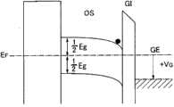
图26A和26B是沿图25中的线A-A′所取的截面的能带图(示意图)。26A and 26B are energy band diagrams (schematic diagrams) of sections taken along line A-A' in FIG. 25 .
图27A是示出其中正电位(+VG)被施加到栅极(GI)的状态的示图,而图27B是示出其中负电位(-VG)被施加到栅极(GI)的状态的示图。27A is a diagram showing a state in which a positive potential (+VG ) is applied to the gate (GI), and FIG. 27B is a diagram showing a state in which a negative potential (-VG ) is applied to the gate (GI). A diagram of the state.
图28是示出真空能级、金属的功函数(φM)、以及氧化物半导体的电子亲和性(χ)之间的关系的示图。FIG. 28 is a graph showing the relationship among the vacuum energy level, the work function (φM) of a metal, and the electron affinity (χ) of an oxide semiconductor.
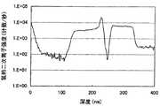
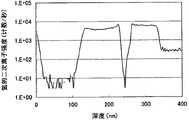
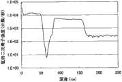
图29A和29B示出通过SIMS对氢的二次离子强度的分析结果。29A and 29B show the results of analysis of the secondary ion strength of hydrogen by SIMS.
图30A和30B示出通过SIMS对氢的二次离子强度的分析结果。30A and 30B show the results of analysis of the secondary ion strength of hydrogen by SIMS.
用于实现本发明的最佳模式Best Mode for Carrying Out the Invention
在下文中,将参考附图详细地描述本发明的各个实施例。然而,本发明不限于以下描述,并且本领域技术人员容易理解,模式和细节可以各种方式改变而不背离本发明的精神与范围。因此,本发明不应被解释为限于以下各个实施例的描述。Hereinafter, various embodiments of the present invention will be described in detail with reference to the accompanying drawings. However, the present invention is not limited to the following description, and it is easily understood by those skilled in the art that modes and details can be changed in various ways without departing from the spirit and scope of the present invention. Therefore, the present invention should not be construed as being limited to the description of each embodiment below.
本发明可应用于制造包括微处理器、诸如图像处理电路之类的集成电路、RF标签、以及半导体显示设备的任何种类的半导体器件。半导体器件是指可通过利用半导体特性而起作用的任何器件,并且半导体显示设备、半导体电路、以及电子设备都包括在半导体器件的范畴内。半导体显示设备在其范畴内包括以下元件:液晶显示设备;其中为每一像素设置以有机发光元件(OLED)为代表的发光元件的发光设备;电子纸;数字微镜设备(DMD);等离子体显示面板(PDP);场发射显示器(FED);以及其中使用半导体膜的电路元件包括在驱动电路中的其他半导体显示设备。The present invention is applicable to the manufacture of any kind of semiconductor devices including microprocessors, integrated circuits such as image processing circuits, RF tags, and semiconductor display devices. A semiconductor device refers to any device that can function by utilizing semiconductor characteristics, and semiconductor display devices, semiconductor circuits, and electronic devices are included in the category of semiconductor devices. The semiconductor display device includes the following elements within its category: a liquid crystal display device; a light emitting device in which a light emitting element typified by an organic light emitting element (OLED) is provided for each pixel; electronic paper; a digital micromirror device (DMD); plasma Display panels (PDPs); field emission displays (FEDs); and other semiconductor display devices in which circuit elements using semiconductor films are included in drive circuits.
(实施例1)(Example 1)
以具有沟道蚀刻结构的底栅薄膜晶体管为例,并且将描述根据本发明的一个实施例的半导体器件中所包括的晶体管的结构。A bottom-gate thin film transistor having a channel-etched structure is taken as an example, and the structure of a transistor included in a semiconductor device according to an embodiment of the present invention will be described.
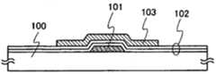
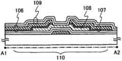
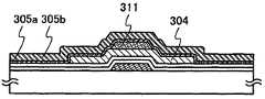
图1A示出薄膜晶体管110的截面图,而图1C示出图1A所示的薄膜晶体管10的俯视图。注意,沿图1C中的虚线A1-A2所取的截面图对应于图1A。FIG. 1A shows a cross-sectional view of the
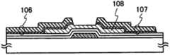
薄膜晶体管110包括在具有绝缘表面的衬底100上形成的栅电极101、栅电极101上的栅绝缘膜102、在栅绝缘膜102上且与栅电极101重叠的氧化物半导体膜108、以及在氧化物半导体膜108上形成的一对源电极106和漏电极107。此外,薄膜晶体管110可包括在氧化物半导体膜108上形成的绝缘膜109作为组件。薄膜晶体管110具有其中蚀刻掉氧化物半导体膜108在源电极106和漏电极107之间的一部分的沟道蚀刻结构。可在栅电极101和衬底100之间设置用作基膜的绝缘膜。The
岛状氧化物半导体膜108以在通过使用氧化物半导体靶的溅射法形成氧化物半导体膜之后、通过蚀刻等将氧化物半导体膜处理成期望形状的方式形成。此外,可在稀有气体(例如,氩气)气氛、氧气气氛、或包含稀有气体(例如,氩气)和氧气的气氛中通过溅射法形成该氧化物半导体膜。岛状氧化物半导体膜108的厚度被设为大于或等于10nm且小于或等于300nm、优选大于或等于20nm且小于或等于100nm。The island-shaped
以上氧化物半导体可用于氧化物半导体膜108。The above oxide semiconductor can be used for the
使用具有充分减小的氢浓度的高度提纯的氧化物半导体膜,在该氧化物半导体膜中去除了氧化物半导体中所包含的杂质(诸如氢或水)以使通过二次离子质谱法(SIMS)所测量的氧化物半导体中的氢浓度值小于或等于5×10¹⁹/cm3、优选小于或等于5×1018/cm3、更优选小于或等于5×1017/cm3,由此晶体管的截止状态电流可减小。A highly purified oxide semiconductor film having a sufficiently reduced hydrogen concentration in which impurities such as hydrogen or water contained in the oxide semiconductor are removed so that ) the measured hydrogen concentration value in the oxide semiconductor is less than or equal to 5×10¹⁹ /cm3 , preferably less than or equal to 5×10¹⁸ /cm3 , more preferably less than or equal to 5×10¹⁷ /cm3 , whereby The off-state current of the transistor can be reduced.
在本实施例中,通过使用包含铟(In)、镓(Ga)、以及锌(Zn)(In2O3∶Ga2O3∶ZnO=1∶1∶1)的氧化物半导体靶的溅射法而获得的厚度为30nm的In-Ga-Zn-O基非单晶膜被用作为氧化物半导体膜108。In this example, the thickness obtained by the sputtering method using an oxide semiconductor target containing indium (In), gallium (Ga), and zinc (Zn) (In2O3:Ga2O3:ZnO=1:1:1) An In-Ga-Zn-O-based non-single-crystal film of 30 nm is used as the
在岛状氧化物半导体膜108上形成源电极和漏电极的导电膜之后,导电膜通过蚀刻等来图案化,从而形成源电极106和漏电极107。当通过以上图案化来形成源电极106和漏电极107时,在一些情况下部分地蚀刻岛状氧化物半导体膜108的暴露部分。因此,如图1A所示,当部分地蚀刻掉氧化物半导体膜108位于源电极106和漏电极107之间的区域时,该区域的厚度变得小于与源电极106或漏电极107重叠的区域的厚度。After the conductive film of the source electrode and the drain electrode is formed on the island-shaped
使用具有低负电性的金属、或者使用该金属的混合物、金属化合物、或合金来形成源电极106和漏电极107,并且源电极106和漏电极107中的氢浓度是氧化物半导体膜108中的氢浓度的1.2倍、优选大于或等于其5倍。The
具体地,源电极106和漏电极107中的氢浓度大于或等于1×10¹⁹/cm3、优选大于或等于5×1018/cm3、更优选大于或等于5×1017/cm3,并且是氧化物半导体膜108中的氢浓度的1.2倍、优选大于或等于其5倍。源电极106和漏电极107中的氢浓度是通过二次离子质谱法(SIMS)所测量的值。Specifically, the hydrogen concentration in the
可给出钛、镁、钇、铝、钨、钼等作为具有低负电性的金属。包含这些金属中的一种或多种的混合物、金属化合物、或者合金可被用作源电极106和漏电极107。此外,以上材料可与耐热导电材料(诸如从钽、铬、钕、以及钪中选择的元素;包含这些元素中的一种或多种作为组分的合金;或者包含该元素作为组分的氮化物)组合。Titanium, magnesium, yttrium, aluminum, tungsten, molybdenum, and the like can be given as the metal having low electronegative property. A mixture, a metal compound, or an alloy containing one or more of these metals may be used as the
在本发明的一个实施例中,由于具有低负电性的金属、或者使用该金属的混合物、金属化合物、或合金用于源电极106和漏电极107,因此存在于氧化物半导体膜108、栅绝缘膜102中、或者氧化物半导体膜108与另一绝缘膜之间的界面处及其附近的杂质(诸如水分或氢)可被用于形成源电极106和漏电极107的导电膜容易地吸取。因此,可通过消除诸如水分或氢之类的杂质来获得作为本征(i型)半导体或基本i型的半导体的氧化物半导体膜108,并且可防止促进晶体管110的特性因杂质造成的劣化(诸如阈值电压的偏移),且可减小截止状态电流。In one embodiment of the present invention, since a metal having low electronegativeness, or a mixture, a metal compound, or an alloy of the metal is used for the
注意,在具有低负电性的金属中,钛、钼、以及钨具有与氧化物半导体膜108的低接触电阻。因此,钛、钼、或钨用于形成源电极106和漏电极107的导电膜,从而可减少氧化物半导体膜108中的杂质,并且可形成具有与氧化物半导体膜108的低接触电阻的源电极106和漏电极107。Note that among metals having low electronegative properties, titanium, molybdenum, and tungsten have low contact resistance with the
另外,通过二次离子质谱法(SIMS),观察到氧化物半导体膜中的氢浓度在形成氧化物半导体膜时的该时刻约为1020/cm3。在本发明中,去除不可避免地存在于氧化物半导体中且形成施主能级的杂质(诸如水或氢),从而氧化物半导体膜被高度提纯为i型(本征)半导体膜。另外,在去除水或氢的情况下,作为氧化物半导体的组分之一的氧也减少。由此,作为本发明的技术思想之一,含氧的绝缘膜被形成为与氧化物半导体膜接触,从而向具有氧空位的氧化物半导体膜供应足够的氧。In addition, by secondary ion mass spectrometry (SIMS), it was observed that the hydrogen concentration in the oxide semiconductor film was about 1020 /cm3 at the time when the oxide semiconductor film was formed. In the present invention, impurities such as water or hydrogen that inevitably exist in an oxide semiconductor and form a donor level are removed, whereby the oxide semiconductor film is highly purified into an i-type (intrinsic) semiconductor film. In addition, in the case of removing water or hydrogen, oxygen which is one of the components of the oxide semiconductor also decreases. Thus, as one of the technical ideas of the present invention, an insulating film containing oxygen is formed in contact with the oxide semiconductor film so as to supply sufficient oxygen to the oxide semiconductor film having oxygen vacancies.
氧化物半导体膜中的氢含量优选尽可能地小,并且氧化物半导体中的载流子优选较少。即,作为一指标,氢浓度小于或等于1×10¹⁹/cm3、优选小于或等于5×1018/cm3、更优选小于或等于5×1017/cm3或者小于或等于1×1016/cm3。另外,载流子密度小于或等于1×1014/cm3、优选小于或等于1×1012/cm3。更理想地,载流子密度基本为0。在本发明中,氧化物半导体膜的载流子密度尽可能地减小,并且其理想载流子密度基本为0;因此,氧化物半导体膜用作从TFT的源电极和漏电极供应的载流子通过的路径。The hydrogen content in the oxide semiconductor film is preferably as small as possible, and the carriers in the oxide semiconductor are preferably less. That is, as an indicator, the hydrogen concentration is less than or equal to 1×10¹⁹ /cm3 , preferably less than or equal to 5×10¹⁸ /cm3 , more preferably less than or equal to 5×10¹⁷ /cm3 or less than or equal to 1×10¹⁶ /cm3 . In addition, the carrier density is less than or equal to 1×10¹⁴ /cm3 , preferably less than or equal to 1×10¹² /cm3 . More ideally, the carrier density is substantially zero. In the present invention, the carrier density of the oxide semiconductor film is reduced as much as possible, and its ideal carrier density is substantially 0; therefore, the oxide semiconductor film serves as a carrier supplied from the source and drain electrodes of the TFT. The path through which the stream passes.
氧化物半导体膜的载流子密度被尽可能地减小到小于1×10¹¹/cm3,并且理想地基本为0;因此,TFT的截止状态电流可减小为尽可能地低。The carrier density of the oxide semiconductor film is reduced as much as possible to less than 1×10¹¹ /cm3 , and ideally substantially 0; therefore, the off-state current of the TFT can be reduced as low as possible.
通过溅射法绝缘膜109形成为与岛状氧化物半导体膜108、源电极106和漏电极107接触。在本实施例中,绝缘膜109被形成为具有其中通过溅射法形成的100nm厚的氮化硅膜层叠在通过溅射法形成的200nm厚的氧化硅膜上的结构。The insulating
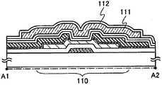
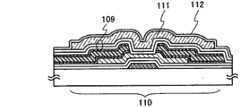
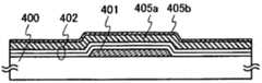
注意,在图1A中,描述其中使用单层导电膜来形成源电极106和漏电极107的情况。然而,本发明的一个实施例不限于该结构,并且例如,可使用层叠的多个导电膜来形成源电极106和漏电极107。图1B是在源电极106和漏电极107各自具有相层叠的第一导电膜105a和第二导电膜105b的情况下的晶体管的截面图。注意,在图1B中,具有类似于图1A所示的晶体管110的功能的部分由相同的附图标记标示。Note that, in FIG. 1A , a case is described in which a single-layer conductive film is used to form
图1B所示的晶体管中的源电极106和漏电极107以如下方式形成:源电极和漏电极的第一导电膜105a和第二导电膜105b层叠在岛状氧化物半导体膜108上,并且随后这些导电膜通过蚀刻等来图案化。因此,源电极106和漏电极107各自具有与氧化物半导体膜108接触的第一导电膜105a以及层叠在第一导电膜105a上的第二导电膜105b。随后,使用具有低负电性的金属、或者使用该金属的混合物、金属化合物、或合金来形成第一导电膜105a,并且第一导电膜105a中的氢浓度是氧化物半导体膜108中的氢浓度的1.2倍、优选大于或等于其5倍。The
具体地,当第一导电膜105a中的氢浓度大于或等于1×10¹⁹/cm3、优选大于或等于5×1018/cm3、且更优选大于或等于5×1017/cm3时,第一导电膜105a中的氢浓度是氧化物半导体膜108中的氢浓度的1.2倍、优选大于或等于其5倍。第一导电膜105a中的氢浓度是通过二次离子质谱法(SIMS)所测量的值。Specifically, when the hydrogen concentration in the first
具体地,第二导电膜105b可被形成为具有使用利用诸如钼、钛、铬、钽、钨、钕、或钪之类的金属材料、包含这些金属材料中的任一种作为其主要组分的合金材料、或者包含这些金属中的任一种的氮化物的一个或多个导电膜的单层结构或叠层结构。注意,对于第二导电膜105b,如果铝或铜可耐受后续工艺中进行的热处理的温度,则也可被用作这种金属材料。铝或铜优选与高熔点(refractory)金属材料组合使用以避免耐热和腐蚀的问题。可使用钼、钛、铬、钽、钨、钕、钪等作为高熔点金属材料。替换地,氧化铟、氧化铟氧化锡合金、氧化铟氧化锌合金、氧化锌、氧化铝锌、氧氮化铝锌、或氧化镓锌的透光氧化物导电膜可被用作第二导电膜105b。Specifically, the second
具体而言,当诸如铝或铜之类的低电阻率材料用于第二导电膜105b时,使用第一导电膜105a和第二导电膜105b而形成的源电极106和漏电极107的组合电阻可减小。Specifically, when a low-resistivity material such as aluminum or copper is used for the second
当使用具有低负电性的金属、或者使用该金属的混合物、金属化合物、或合金来形成与氧化物半导体膜108接触的第一导电膜105a时,存在于氧化物半导体膜108、栅绝缘膜102中、或者氧化物半导体膜108与另一绝缘膜之间的界面处及其附近的杂质(诸如水分或氢)可被第二导电膜105b容易地吸取,如在图1A中。因此,可通过消除诸如水分或氢之类的杂质来获得作为本征(i型)半导体或基本i型半导体的氧化物半导体膜108,并且可防止促进晶体管110的特性因杂质造成的劣化(诸如阈值电压的偏移),且可减小截止状态电流。When the first
注意,在具有低负电性的金属之间,钛、钼、以及钨具有与氧化物半导体膜108的低接触电阻。因此,钛、钼、或钨用于第一导电膜105a,从而可减少氧化物半导体膜108中的杂质,并且可形成具有与氧化物半导体膜108的低接触电阻的源电极106和漏电极107。Note that among metals having low electronegative properties, titanium, molybdenum, and tungsten have low contact resistance with the
接着,具有图1B所示的沟道蚀刻结构的底栅薄膜晶体管被用作一示例,并且将参考图2A至2E以及图3A至3C来描述半导体器件的更详细结构及其制造方法。Next, a bottom-gate thin film transistor having a channel-etched structure shown in FIG. 1B is used as an example, and a more detailed structure of the semiconductor device and its manufacturing method will be described with reference to FIGS. 2A to 2E and FIGS. 3A to 3C .
如图2A所示,在衬底100上形成栅电极101。As shown in FIG. 2A , a
可在衬底100和栅电极101之间形成用作基膜的绝缘膜。例如,可使用氧化硅膜、氧氮化硅膜、氮化硅膜、氮氧化硅膜、氮化铝膜、以及氮氧化铝膜中的任一个或多个的单层或叠层来作为基膜。具体而言,具有高阻挡性的绝缘膜(例如,氮化硅膜、氮氧化硅膜、氮化铝膜、或氮氧化铝膜)用于基膜,从而可防止气氛中的杂质(诸如水分或氢)、或者衬底100中所包括的杂质(诸如碱金属或重金属)进入氧化物半导体膜、栅绝缘膜、或者氧化物半导体膜与另一绝缘膜之间的界面及其附近。An insulating film serving as a base film may be formed between the
在本说明书中,氧氮化物是指含氧量大于含氮量的物质,而氮氧化物是指含氮量大于含氧量的物质。In this specification, oxynitride refers to a substance containing more oxygen than nitrogen, and nitrogen oxide refers to a substance containing nitrogen more than oxygen.
栅电极101可被形成为具有使用利用诸如钼、钛、铬、钽、钨、钕、或钪之类的金属材料、包含这些金属材料中的任一种作为其主要组分的合金材料、或者包含这些金属中的任一种的氮化物的一个或多个导电膜的单层或叠层。注意,如果铝或铜可耐受后续工艺中进行的热处理的温度,则也可被用作这种金属材料。铝或铜优选与高熔点金属材料组合以避免耐热和腐蚀的问题。可使用钼、钛、铬、钽、钨、钕、钪等作为高熔点金属材料。The
例如,作为栅电极101的双层结构,以下结构是优选的:其中钼膜层叠在铝膜上的双层结构,其中钼膜层叠在铜膜上的双层结构,其中氮化钛膜或氮化钽膜层叠在铜膜上的双层结构,以及氮化钛膜和钼膜层叠的双层结构。作为栅电极101的三层结构,以下结构是优选的:包含铝膜、铝和硅的合金膜、铝和钛的合金膜,或者中间层中的铝和钕的合金膜、以及顶层和底层中的钨膜、氮化钨膜、氮化钛膜、以及钛膜中的任一种的层叠结构。For example, as the double-layer structure of the
此外,氧化铟、氧化铟氧化锡合金、氧化铟氧化锌合金、氧化锌、氧化铝锌、氧氮化铝锌、氧化镓锌等的透光氧化物导电膜被用作栅电极101,从而可增加像素部分的开口率。In addition, a light-transmitting oxide conductive film of indium oxide, indium oxide tin oxide alloy, indium oxide zinc oxide alloy, zinc oxide, aluminum zinc oxide, aluminum zinc oxynitride, gallium zinc oxide, etc. is used as the
栅电极101的厚度为10nm至400nm、优选为100nm至200nm。在本实施例中,在通过使用钨靶的溅射法将栅电极的导电膜形成为具有150nm的厚度之后,通过蚀刻将导电膜处理(图案化)成期望形状,由此形成栅电极101。The thickness of the
接着,在栅电极101上形成栅绝缘膜102。可通过等离子体增强的CVD法、溅射法等将栅绝缘膜102形成为具有单层的氧化硅膜、氮化硅膜、氧氮化硅膜、氮氧化硅膜、氧化铝膜、或氧化钽膜、或者其叠层。优选栅绝缘膜102包括尽可能少的杂质,诸如水分或氢。栅绝缘膜102可具有其中使用具有高阻挡性的材料形成的绝缘膜、以及具有较低比例的氮的绝缘膜(诸如氧化硅膜或氧氮化硅膜)层叠的结构。在此情况下,在具有阻挡性的绝缘膜和氧化物半导体膜之间形成绝缘膜,诸如氧化硅膜或氧氮化硅膜。例如,可给出氮化硅膜、氮氧化硅膜、氮化铝膜、氮氧化铝膜等作为具有高阻挡性的绝缘膜。使用具有阻挡性的绝缘膜,从而可防止气氛中的杂质(诸如水分或氢)、或者衬底中所包括的杂质(诸如碱金属或重金属)进入氧化物半导体膜、栅绝缘膜102、或者氧化物半导体膜与另一绝缘膜之间的界面及其附近。另外,具有较低比例的氮的绝缘膜(诸如氧化硅膜或氧氮化硅膜)被形成为与氧化物半导体膜接触,从而可防止使用具有高阻挡性的材料形成的绝缘膜与氧化物半导体膜直接接触。Next, a
在本实施例中,栅绝缘膜102被形成为具有其中通过溅射法形成的100nm厚的氧化硅膜层叠在通过溅射法形成的50nm厚的氮化硅膜上的结构。In the present embodiment,
接着,在栅绝缘膜102上形成氧化物半导体膜。该氧化物半导体膜通过使用氧化物半导体靶的溅射法来形成。此外,可在稀有气体(例如,氩气)气氛、氧气气氛、或者包含稀有气体(例如,氩气)和氧气的气氛中通过溅射法形成该氧化物半导体膜。Next, an oxide semiconductor film is formed on the
注意,在通过溅射法形成氧化物半导体膜之前,优选通过导入氩气并生成等离子体的反溅射来去除附着到栅绝缘膜102的表面的灰尘。反溅射是指其中在未向靶侧施加电压的情况下,RF电源用于在氩气气氛中向基板侧施加电压、从而在衬底附近生成等离子体以使表面改性的方法。注意,可使用氮气气氛、氦气气氛等来代替氩气气氛。替换地,可使用添加了氧气、一氧化二氮等的氩气气氛。替换地,可使用添加了氯气、四氟化碳等的氩气气氛。Note that before forming the oxide semiconductor film by the sputtering method, it is preferable to remove dust adhering to the surface of the
对于氧化物半导体膜,可使用如以上所述的氧化物半导体。For the oxide semiconductor film, an oxide semiconductor as described above can be used.
氧化物半导体膜的厚度被设为10nm至300nm、优选20nm至100nm。在本实施例中,使用通过使用包含铟(In)、镓(Ga)、以及锌(Zn)(摩尔比In2O3∶Ga2O3∶ZnO=1∶1∶1或1∶1∶2)的氧化物半导体靶的溅射法而获得的厚度为30nm的In-Ga-Zn-O基非单晶膜来作为氧化物半导体膜。在本实施例中,采用DC溅射法,氩气的流速为30sccm,氧气的流速为15sccm,并且衬底温度是室温。The thickness of the oxide semiconductor film is set to 10 nm to 300 nm, preferably 20 nm to 100 nm. In the present embodiment, the use includes indium (In), gallium (Ga), and zinc (Zn) (molar ratio In2 O3 :Ga2 O3 : ZnO=1:1:1 or 1:1:1 2) An In-Ga-Zn-O-based non-single crystal film with a thickness of 30 nm obtained by the sputtering method of the oxide semiconductor target was used as the oxide semiconductor film. In this embodiment, the DC sputtering method is used, the flow rate of argon gas is 30 sccm, the flow rate of oxygen gas is 15 sccm, and the substrate temperature is room temperature.
可在不暴露给空气的情况下连续地形成栅绝缘膜102和氧化物半导体膜。在不暴露给空气的情况下连续的膜形成可能获得叠层之间的每一界面,该界面不受大气组分或在空气中漂浮的杂质元素(诸如水、碳氢化合物)污染。因此,可减少薄膜晶体管的特性变化。The
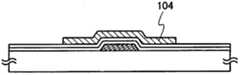
接着,如图2A所示,通过蚀刻等将氧化物半导体膜处理(图案化)成期望形状,由此在岛状氧化物半导体膜103与栅电极101重叠的位置处岛状氧化物半导体膜103在栅绝缘膜102上形成。Next, as shown in FIG. 2A , the oxide semiconductor film is processed (patterned) into a desired shape by etching or the like, whereby the island-shaped
然后,可在还原气氛、氮气、稀有气体等的惰性气体气氛、氧气气氛、或超干空气气氛(在其水分含量在使用腔衰荡激光谱(CRDS)系统的露点表来进行测量的情况下小于或等于20ppm(露点变换,-55℃)、优选小于或等于1ppm、更优选小于或等于10ppb的空气中)中对氧化物半导体膜103进行热处理。当对氧化物半导体膜103进行热处理时,形成其中消除了水分或氢的氧化物半导体膜104。具体地,可在惰性气体(氮气、氦气、氖气、氩气等)气氛中,在高于或等于500℃且低于或等于750℃(或者低于或等于玻璃衬底的应变点)的温度下进行快速热退火(RTA)处理约大于或等于1分钟且小于或等于10分钟,优选在600℃的温度下进行该RTA处理约大于或等于3分钟且小于或等于6分钟。由于可通过RTA法在短时间内进行脱水或脱氢,因此即使在高于玻璃基板的应变点的温度下也可进行处理。注意,在形成岛状氧化物半导体膜103之后不一定进行热处理,而在形成岛状氧化物半导体膜103之前对氧化物半导体膜进行热处理。可在形成氧化物半导体膜104之后进行一次以上的热处理。通过热处理来消除诸如水分或氢之类的杂质,从而岛状氧化物半导体膜104变成本征(i型)半导体或基本i型的半导体;因此,可防止促进晶体管的特性因杂质造成的劣化,并且可减小截止状态电流。Then, in a reducing atmosphere, an inert gas atmosphere such as nitrogen, a rare gas, an oxygen atmosphere, or an ultra-dry air atmosphere (in the case where the moisture content is measured using a dew point meter of a cavity ring-down laser spectroscopy (CRDS) system The
在本实施例中,在衬底温度达到设定温度的状态中,在氮气气氛中在600℃下进行热处理达6分钟。此外,使用电炉的加热法、诸如使用加热气体的气体快速热退火(GRTA)法或使用灯光的灯快速热退火(LRTA)法之类的快速加热法等可用于该热处理。例如,在使用电炉进行热处理的情况下,温度上升特性优选被设为高于或等于0.1℃/分钟且低于或等于20℃/分钟,而温度下降特性优选被设为高于或等于0.1℃/分钟且低于或等于15℃/分钟。In the present embodiment, heat treatment was performed at 600° C. for 6 minutes in a nitrogen atmosphere in a state where the substrate temperature reached the set temperature. In addition, a heating method using an electric furnace, a rapid heating method such as a gas rapid thermal annealing (GRTA) method using a heating gas or a lamp rapid thermal annealing (LRTA) method using a lamp, or the like can be used for the heat treatment. For example, in the case of heat treatment using an electric furnace, the temperature rise characteristic is preferably set to be higher than or equal to 0.1°C/minute and lower than or equal to 20°C/minute, and the temperature drop characteristic is preferably set to be higher than or equal to 0.1°C /min and less than or equal to 15°C/min.
注意,优选在热处理中,在氮气、或者诸如氦气、氖气或氩气之类的稀有气体中不包含水分、氢等。替换地,优选导入热处理装置的氮气、或者诸如氦气、氖气或氩气之类的稀有气体的纯度被设为高于或等于6N(99.9999%)、优选高于或等于7N(99.99999%)(即,杂质浓度低于或等于1ppm、优选低于或等于0.1ppm)。Note that it is preferable not to contain moisture, hydrogen, or the like in nitrogen, or a rare gas such as helium, neon, or argon in the heat treatment. Alternatively, the purity of nitrogen, or a rare gas such as helium, neon or argon, which is preferably introduced into the heat treatment device is set to be higher than or equal to 6N (99.9999%), preferably higher than or equal to 7N (99.99999%) (ie, the impurity concentration is lower than or equal to 1 ppm, preferably lower than or equal to 0.1 ppm).
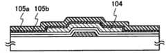
接着,如图2C所示,在岛状氧化物半导体膜104上形成用于源电极和漏电极的导电膜。在本实施例中,使用具有低负电性的金属、或者使用该金属的混合物、金属化合物、或合金的第一导电膜105a被形成为与氧化物半导体膜104接触,并且随后第二导电膜105b层叠在第一导电膜105a上。Next, as shown in FIG. 2C , a conductive film for a source electrode and a drain electrode is formed on the island-shaped
可给出钛、镁、钇、铝、钨、钼等作为具有低负电性的金属。包含这些金属中的一种或多种的混合物、金属化合物、或者合金可被用作第一导电膜105a。此外,以上材料可与耐热导电材料(诸如从钽、铬、钕、以及钪中选择的元素;包含这些元素中的一种或多种作为组分的合金;或者包含该元素作为组分的氮化物)组合。Titanium, magnesium, yttrium, aluminum, tungsten, molybdenum, and the like can be given as the metal having low electronegative property. A mixture, metal compound, or alloy containing one or more of these metals can be used as the first
具体地,第二导电膜105b可被形成为具有使用利用诸如钼、钛、铬、钽、钨、钕、或钪之类的金属材料、包含这些金属材料中的任一种作为其主要组分的合金材料、或者包含这些金属中的任一种的氮化物的一个或多个导电膜的单层结构或叠层结构。注意,对于第二导电膜105b,如果铝或铜可耐受后续工艺中进行热处理的温度,则也可被用作这种金属材料。铝或铜优选与高熔点金属材料组合使用以避免耐热和腐蚀的问题。可使用钼、钛、铬、钽、钨、钕、钪等作为高熔点金属材料。替换地,氧化铟、氧化铟氧化锡合金、氧化铟氧化锌合金、氧化锌、氧化铝锌、氧氮化铝锌、或氧化镓锌的透光氧化物导电膜可被用作第二导电膜105b。Specifically, the second
具体而言,当诸如铝或铜之类的低电阻率材料用于第二导电膜105b时,使用第一导电膜105a和第二导电膜105b形成的源电极106和漏电极107的组合电阻可减小。Specifically, when a low-resistivity material such as aluminum or copper is used for the second
第一导电膜105a的厚度优选为10nm至200nm、更优选为50nm至150nm。第二导电膜105b的厚度优选为100nm至300nm、更优选为150nm至250nm。在本实施例中,通过溅射法形成的100nm厚的钛膜被用作第一导电膜105a,而通过溅射法形成的200nm厚的铝膜被用作第二导电膜105b。The thickness of the first
在本发明的一个实施例中,使用具有低负电性的金属、或者使用该金属的混合物、金属化合物、或合金来形成第一导电膜105a,从而存在于氧化物半导体膜104、栅绝缘膜102中、或者氧化物半导体膜104与另一绝缘膜之间的界面处及其附近的杂质(诸如水分或氢)被第一导电膜105a吸取。因此,通过消除诸如水分或氢之类的杂质,可获得作为本征(i型)半导体或基本i型半导体的氧化物半导体膜108,并且可防止促进晶体管的特性因杂质造成的劣化(诸如阈值电压的偏移),且可减小截止状态电流。In one embodiment of the present invention, the first
除了以上结构以外,所暴露的第二导电膜105b可在诸如氮气气氛或稀有气体(氩气、氦气等)气氛之类的惰性气体气氛中进行热处理,从而可促进对诸如氢或水之类的杂质的吸取。用于促进吸取的热处理的温度范围优选高于或等于100℃且低于或等于350℃、更优选高于或等于220℃且低于或等于280℃。进行热处理以使存在于氧化物半导体膜104、栅绝缘膜102中、或者氧化物半导体膜104与另一栅绝缘膜之间的界面处及其附近的杂质(诸如水分或氢)可被第一导电膜105a容易地吸取。In addition to the above structure, the exposed second
接着,如图2D所示,通过蚀刻等将第一导电膜105a和第二导电膜105b处理(图案化)成期望形状,由此形成源电极106和漏电极107。例如,当钛膜用于第一导电膜105a而铝膜用于第二导电膜105b时,在使用含磷酸的溶液对第二导电膜105b进行湿法蚀刻之后,可使用含氨和双氧水的溶液(氨双氧水混合物)对第一导电膜105a进行湿法蚀刻。具体地,在本实施例中,由沃克纯化学工业有限公司(Wako Pure Chemical Industries,Ltd.)生产的Al-蚀刻剂(包含2.0wt%的硝酸、9.8wt%的醋酸、以及72.3wt%的磷酸的水溶液)被用作含磷酸的溶液。另外,具体地,使用其中31wt%的双氧水、28wt%的氨水、以及水以5∶2∶2的体积比混合的水溶液作为氨双氧水混合物。替换地,可使用包含氯(Cl2)、氯化硼(BCl3)等的气体对第一导电膜105a和第二导电膜105b进行干法蚀刻。Next, as shown in FIG. 2D , the first
当通过图案化来形成源电极106和漏电极107时,在一些情况下蚀刻掉岛状氧化物半导体膜104的暴露部分的一部分。在本实施例中,描述形成具有凹槽(凹陷部分)的岛状氧化物半导体膜108的情况。When the
注意,如图2E所示,在形成源电极106和漏电极107之后,绝缘膜109被形成为覆盖源电极106、漏电极107、以及氧化物半导体膜108。绝缘膜109优选包括尽可能少的杂质(诸如水分或氢),并且绝缘膜109可使用单层绝缘膜或层叠的多个绝缘膜来形成。具有高阻挡性的材料优选用于绝缘膜109。例如,可使用氮化硅膜、氮氧化硅膜、氮化铝膜、氮氧化铝膜等作为具有高阻挡性的绝缘膜。当使用层叠的多个绝缘膜时,在更接近氧化物半导体膜108的一侧上形成其氮的比例比具有阻挡性的绝缘膜(诸如氧化硅膜或氧氮化硅膜)低的绝缘膜。然后,具有阻挡性的绝缘膜被形成为与源电极106、漏电极107、以及氧化物半导体膜108重叠,其中在具有阻挡性的绝缘膜与源电极106、漏电极107、以及氧化物半导体膜108之间具有氮的比例较低的绝缘膜。当使用具有阻挡性的绝缘膜时,可防止诸如水分或氢之类的杂质进入氧化物半导体膜108、栅绝缘膜102、或者氧化物半导体膜108与另一绝缘膜之间的界面及其附近。另外,具有较低比例氮的绝缘膜(诸如氧化硅膜或氧氮化硅膜)被形成为与氧化物半导体膜108接触,从而可防止使用具有高阻挡性的材料形成的绝缘膜与氧化物半导体膜直接接触。Note that, as shown in FIG. 2E , after the
在本实施例中,绝缘膜109被形成为具有其中通过溅射法形成的100nm厚的氮化硅膜层叠在通过溅射法形成的200nm厚的氧化硅膜上的结构。膜形成时的衬底温度可高于或等于室温且低于或等于300℃,且在本实施例中为100℃。In the present embodiment, the insulating
氧化物半导体膜108设置在源电极106和漏电极107之间的暴露区域、以及形成绝缘膜109的氧化硅被设置成彼此接触,从而通过供氧来增大氧化物半导体膜108与绝缘膜109接触的区域的电阻,由此可形成包括具有高电阻的沟道形成区的氧化物半导体膜108。The
注意,可在形成绝缘膜109之后进行热处理。该热处理优选在空气气氛或惰性气体(氮气、氦气、氖气、或氩气)气氛中在高于或等于200℃且低于或等于400℃(例如,高于或等于250℃且低于或等于350℃)的温度下进行。例如,在本实施例中,在氮气气氛中在250℃下进行热处理达1小时。替换地,在形成第一导电膜105a和第二导电膜105b之前,在高温下短时间的RTA处理可以类似于对氧化物半导体膜进行的热处理的方式进行。通过热处理,氧化物半导体膜108在与形成绝缘膜109的氧化硅接触时进行加热。另外,通过向氧化物半导体膜108供应氧来增大氧化物半导体膜108的电阻。因此,可改进晶体管的电特性,并且可减小其电特性的变化。对何时进行该热处理没有具体限制,只要它在形成绝缘膜109之后进行即可。当该热处理还用作另一步骤中的热处理(例如,形成树脂膜时的热处理、或者用于减小透明导电膜的电阻的热处理)时,可防止步骤的数量增加。Note that heat treatment may be performed after the insulating
接着,如图3A所示,在绝缘膜109上形成导电膜之后,将导电膜图案化,从而背栅电极111可被形成为与氧化物半导体膜108重叠。可使用类似于栅电极101或者源电极106和漏电极107的材料和结构来形成背栅电极111。Next, as shown in FIG. 3A , after forming a conductive film on the insulating
背栅电极111的厚度为10nm至400nm、优选为100nm至200nm。在本实施例中,形成其中钛膜、铝膜、以及钽膜按顺序层叠的导电膜。然后,通过光刻法形成蚀刻剂掩模,通过蚀刻来去除不必要的部分,并且将导电膜处理成(图案化)成期望形状,由此形成背栅电极111。The thickness of the
接着,如图3B所示,绝缘膜112被形成为覆盖背栅电极111。优选使用具有高阻挡性的材料来形成绝缘膜112,该具有高阻挡性的材料可防止气氛中的水分、氢、氧等影响晶体管110的特性。例如,可通过等离子体增强的CVD法、溅射法等将绝缘膜112形成为具有使用具有高阻挡性的绝缘膜(诸如氮化硅膜、氮氧化硅膜、氮化铝膜、氮氧化铝膜等)的单层或叠层。绝缘膜112优选形成为具有例如15nm至400nm的厚度以获得阻挡性的效果。Next, as shown in FIG. 3B , an insulating
在本实施例中,通过等离子体增强的CVD法将绝缘膜形成为具有300nm的厚度。绝缘膜在以下条件下形成:硅烷气体的流速为4sccm;一氧化二氮(N2O)的流速为800sccm;并且衬底温度为400℃。In this embodiment, the insulating film is formed to have a thickness of 300 nm by plasma enhanced CVD method. The insulating film was formed under the following conditions: the flow rate of silane gas was 4 sccm; the flow rate of dinitrogen monoxide (N2 O) was 800 sccm; and the substrate temperature was 400°C.
图3C是图3B中的半导体器件的俯视图。图3B对应于沿图3C中的虚线A1-A2所取的截面图。FIG. 3C is a top view of the semiconductor device in FIG. 3B. FIG. 3B corresponds to a cross-sectional view taken along the dotted line A1-A2 in FIG. 3C.
注意,在图3B中,示出背栅电极111覆盖整个氧化物半导体膜108的情况;然而,本发明的一个实施例不限于该结构。背栅电极111可与氧化物半导体膜108中所包括的沟道形成区的至少一部分重叠。Note that in FIG. 3B , a case where the
背栅电极111可处于浮动状态(即,电隔离)、或处于施加一电位的状态。在后者状态中,可向背栅电极111施加与栅电极101相同电平的电位,或者可向其施加诸如接地之类的固定电位。控制施加到背栅电极111的电位电平,从而可控制晶体管110的阈值电压。The
注意,可使用具有三层或更多个层的导电膜来形成晶体管110中的源电极106和漏电极107。图4A是在使用层叠的第一导电膜105a、第二导电膜105b、以及第三导电膜105c来形成源电极106和漏电极107的情况下的晶体管110的截面图。第三导电膜105c可使用与第一导电膜105a和第二导电膜105b相同的材料来形成。注意,当使用三层导电膜来形成源电极106和漏电极107时,不太可能被氧化的导电材料用于第三导电膜105c,从而可防止第二导电膜105b的表面被氧化。作为在防止氧化时有效的材料,例如,钛、钽、钨、钼、铬、钕、或钪、包含这些金属中的一种或多种的混合物、金属化合物、或者合金可用于第三导电膜105c。Note that the
另外,图4A所示的晶体管110可具有如图3B中的背栅电极111。当图4A所示的晶体管110设置有背栅电极111时,晶体管110的结构在图4B中示出。可使用类似于栅电极101或者源电极106和漏电极107的材料和结构来形成背栅电极111。In addition, the
如在本实施例中,将描述通过尽可能多地去除杂质(氧化物半导体膜中所包含的氢、水等)而高度提纯氧化物半导体膜会如何影响晶体管的特性。As in this embodiment, how highly purifying the oxide semiconductor film by removing impurities (hydrogen, water, etc. contained in the oxide semiconductor film) as much as possible will affect the characteristics of the transistor will be described.
图25是使用氧化物半导体形成的倒交错薄膜晶体管的纵向截面图。氧化物半导体膜(OS)隔着栅绝缘膜(GI)设置在栅电极(GE)上,并且源电极(S)和漏电极(D)设置在该栅绝缘膜上。25 is a longitudinal sectional view of an inverted staggered thin film transistor formed using an oxide semiconductor. An oxide semiconductor film (OS) is provided on the gate electrode (GE) via a gate insulating film (GI), and a source electrode (S) and a drain electrode (D) are provided on the gate insulating film.
图26A和26B是沿图25中的线A-A′所取的截面的能带图(示意图)。图26A示出源电极和漏电极之间的电压是等电位(VD=0V)的情况,而图26B示出当源电极的电位用作基准电位时为正的电位被施加到漏电极(VD>0)的情况。26A and 26B are energy band diagrams (schematic diagrams) of sections taken along line AA' in FIG. 25 . 26A shows a case where the voltages between the source electrode and the drain electrode are equipotential (VD =0 V), and FIG. 26B shows that when the potential of the source electrode is used as a reference potential, a positive potential is applied to the drain electrode ( VD >0).
图27A和27B是沿图25中的线B-B′所取的截面的能带图(示意图)。图27A示出其中正电位(+VG)被施加到栅电极(GE)的状态、以及载流子(电子)在源电极和漏电极之间流动的导通状态。图27B示出负电位(-VG)被施加到栅极(GE)的状态、以及截止状态(其中少数载流子不流动)。27A and 27B are energy band diagrams (schematic diagrams) of sections taken along line BB' in FIG. 25 . FIG. 27A shows a state in which a positive potential (+VG ) is applied to the gate electrode (GE), and a conduction state in which carriers (electrons) flow between the source electrode and the drain electrode. FIG. 27B shows a state where a negative potential (-VG ) is applied to the gate (GE), and an off state (in which minority carriers do not flow).
图28示出真空能级、金属的功函数(φM)、以及氧化物半导体的电子亲和性(χ)之间的关系。FIG. 28 shows the relationship among the vacuum energy level, the work function (φM) of a metal, and the electron affinity (χ) of an oxide semiconductor.
由于金属简并,因此导带对应于费米能级。另一方面,一般而言,常规氧化物半导体是n型半导体,并且其费米能级(EF)的位置更接近远离位于导带中心的本征费米能级(Ei)的导带(Ec)。注意,已知氧化物半导体中的氢是施主、并且是使氧化物半导体成为n型半导体的因素之一。Due to the degeneracy of metals, the conduction band corresponds to the Fermi level. On the other hand, in general, a conventional oxide semiconductor is an n-type semiconductor, and the position of its Fermi level (EF ) is closer to the conduction band ( Ec). Note that it is known that hydrogen in an oxide semiconductor is a donor and is one of factors that make an oxide semiconductor an n-type semiconductor.
另一方面,根据本发明的一个实施例,当负电性比氢低的金属用于源电极或漏电极的导电膜时,从氧化物半导体去除作为n型杂质的氢,并且高度提纯氧化物半导体,从而尽可能少地包括不是氧化物半导体的主要组分的杂质以使氧化物半导体可成为本征(i型)半导体。即,不通过添加杂质而通过尽可能多地去除杂质(诸如氢或水)以具有高纯度,氧化物半导体变成i型半导体,从而获得作为本征(i型)半导体或基本本征(i型)的半导体的氧化物半导体。在以上结构的情况下,费米能级(EF)可基本接近与本征费米能级(Ei)相同的电平,如箭头所指示的。On the other hand, according to one embodiment of the present invention, when a metal less electronegative than hydrogen is used for the conductive film of the source electrode or the drain electrode, hydrogen as an n-type impurity is removed from the oxide semiconductor, and the oxide semiconductor is highly purified , thereby including as little as possible impurities which are not main components of the oxide semiconductor so that the oxide semiconductor can become an intrinsic (i-type) semiconductor. That is, by removing impurities such as hydrogen or water as much as possible to have high purity not by adding impurities, the oxide semiconductor becomes an i-type semiconductor, thereby obtaining an i-type semiconductor as an intrinsic (i-type) semiconductor or a substantially intrinsic (i-type) semiconductor. type) semiconductor oxide semiconductor. In the case of the above structure, the Fermi level (EF ) may be substantially close to the same level as the intrinsic Fermi level (Ei), as indicated by the arrow.
当氧化物半导体的带隙(Eg)为3.15eV时,电子亲和性(χ)据说为4.3eV。形成源电极和漏电极的钛(Ti)的功函数约等于氧化物半导体的电子亲和性(χ)。在此情况下,在金属和氧化物半导体之间的界面处不形成电子的肖特基势垒。When the bandgap (Eg) of the oxide semiconductor is 3.15eV, the electron affinity (χ) is said to be 4.3eV. The work function of titanium (Ti) forming the source and drain electrodes is approximately equal to the electron affinity (χ) of the oxide semiconductor. In this case, a Schottky barrier for electrons is not formed at the interface between the metal and the oxide semiconductor.
即,在金属的功函数(φM)等于氧化物半导体的电子亲和性(χ)的情况下,当氧化物半导体与源电极或漏电极彼此接触时,能带图(示意图)如图26A所示。That is, in the case where the work function (φM) of the metal is equal to the electron affinity (χ) of the oxide semiconductor, when the oxide semiconductor and the source electrode or the drain electrode are in contact with each other, the energy band diagram (schematic diagram) is as shown in FIG. 26A Show.
在图26B中,黑点(●)指示电子,并且当正电位被施加到漏电极时,跨过势垒(h)的电子被注入氧化物半导体,并且流向漏电极。在此情况下,势垒的高度(h)根据栅电压和漏电压而改变。当施加正的漏电压时,势垒的高度(h)小于图26A中未施加电压的势垒的高度(h),即,带隙(Eg)的1/2。In FIG. 26B , black dots (●) indicate electrons, and when a positive potential is applied to the drain electrode, electrons crossing the potential barrier (h) are injected into the oxide semiconductor, and flow toward the drain electrode. In this case, the height (h) of the potential barrier changes according to the gate voltage and the drain voltage. When a positive drain voltage is applied, the height (h) of the potential barrier is smaller than that of FIG. 26A with no voltage applied, ie, 1/2 of the bandgap (Eg).
此时,在栅绝缘膜和如图27A所示的高度提纯的氧化物半导体之间的界面处,电子沿着氧化物半导体的能量稳定的最低部分移动。At this time, at the interface between the gate insulating film and the highly purified oxide semiconductor as shown in FIG. 27A , electrons move along the lowest portion where the energy of the oxide semiconductor is stable.
在图27B中,当负电位(反向偏压)被施加至栅电极(GE)时,作为少数载流子的空穴的数量基本为0;由此,电流值变成尽可能地接近于0的值。In FIG. 27B, when a negative potential (reverse bias voltage) is applied to the gate electrode (GE), the number of holes as minority carriers is substantially 0; thus, the current value becomes as close as possible to value of 0.
如上所述,氧化物半导体膜被高度提纯,从而使不是氧化物半导体的主要组分的杂质(诸如水或氢)的量最小化,由此可获得薄膜晶体管的良好操作。As described above, the oxide semiconductor film is highly purified so that the amount of impurities such as water or hydrogen which are not main components of the oxide semiconductor is minimized, whereby good operation of the thin film transistor can be obtained.
接着,将描述对氧化物半导体膜和导电膜层叠的样本进行氢在膜厚方向上的二次离子强度分布的分析的结果。Next, the results of analysis of the secondary ion intensity distribution of hydrogen in the film thickness direction performed on a sample in which an oxide semiconductor film and a conductive film are laminated will be described.
首先,将描述用于该分析的样本的结构及其制造方法。四个样本(样本A至D)用于该分析。对于这些样本中每一个,厚度约为80nm的氧氮化硅膜、以及厚度约为30nm的In-Gz-Zn-O膜按顺序层叠在厚度为0.7mm的玻璃衬底上,并且随后这些膜在氮气气氛中在600℃下进行热处理达6分钟。此外,对于样本A和样本B,厚度约为100nm的钛膜、以及厚度约为140nm的铝膜按顺序层叠在In-Ga-Zn-O膜上,而对于样本C和样本D,厚度约为50nm的钛膜在In-Ga-Zn-O膜上形成。最后,样本B和样本D在氮气气氛中在250℃下进行热处理达1小时。First, the structure of the sample used for this analysis and its manufacturing method will be described. Four samples (Samples A to D) were used for this analysis. For each of these samples, a silicon oxynitride film with a thickness of about 80 nm, and an In-Gz-Zn-O film with a thickness of about 30 nm were sequentially laminated on a glass substrate with a thickness of 0.7 mm, and then the films Heat treatment was performed at 600° C. for 6 minutes in a nitrogen atmosphere. In addition, for sample A and sample B, a titanium film with a thickness of about 100 nm and an aluminum film with a thickness of about 140 nm are sequentially stacked on the In-Ga-Zn-O film, while for samples C and D, a thickness of about A 50 nm titanium film is formed on the In-Ga-Zn-O film. Finally, Sample B and Sample D were heat-treated at 250° C. for 1 hour in a nitrogen atmosphere.
氢的二级离子强度分布通过二级离子质谱法(SIMS)来分析。对样本A、样本B、样本C、以及样本D的SIMS分析分别在图29A、29B、图30A、以及图30B中示出,它们示出氢在膜厚方向上的二级离子强度分布。水平轴示出距样本表面的深度,而左边0nm的深度对应于样本表面的大致位置。垂直轴示出氢在对数标尺上的二级离子强度。在距作为离玻璃衬底最远的表面的铝膜的方向上分析图29A的样本A、以及图29B的样本B。在距作为离玻璃衬底最远的表面的钛膜的方向上分析图30A的样本C、以及图30B的样本D。The secondary ion intensity distribution of hydrogen was analyzed by secondary ion mass spectrometry (SIMS). SIMS analysis of Sample A, Sample B, Sample C, and Sample D are shown in FIGS. 29A , 29B, 30A, and 30B, respectively, which show the secondary ion intensity distribution of hydrogen in the film thickness direction. The horizontal axis shows the depth from the sample surface, while a depth of 0 nm to the left corresponds to the approximate position of the sample surface. The vertical axis shows the secondary ion strength of hydrogen on a logarithmic scale. Sample A of FIG. 29A , and Sample B of FIG. 29B were analyzed in the direction from the aluminum film which is the surface farthest from the glass substrate. Sample C of FIG. 30A , and Sample D of FIG. 30B were analyzed in the direction of the titanium film as the surface farthest from the glass substrate.
已发现,根据图29A的样本A以及图29B的样本B中的氢的二级离子强度分布,示出二次离子强度急剧下降的谷状峰出现在具有In-Ga-Zn-O膜的区域中,在该区域中距样本表面的深度为从约240nm到约270nm。另外,已发现,根据图30A的样本C以及图30B的样本D中的氢的二级离子强度分布,示出二次离子强度显著下降的谷状峰出现在具有In-Ga-Zn-O膜的区域中,在该区域中距样本表面的深度为从约50nm到约80nm。It was found that, from the secondary ion intensity distributions of hydrogen in sample A of FIG. 29A and sample B of FIG. 29B , valley-like peaks showing a sharp drop in secondary ion intensity appear in the region with the In-Ga-Zn-O film , the depth from the sample surface in this region is from about 240 nm to about 270 nm. In addition, it was found that, according to the secondary ion intensity distribution of hydrogen in sample C of FIG. 30A and sample D of FIG. 30B , valley-like peaks showing a significant decrease in secondary ion intensity appear in A region in which the depth from the sample surface is from about 50 nm to about 80 nm.
已发现,根据图29A所示样本A的氢的二级离子强度分布以及图30A所示样本C的氢的二级离子强度分布,在进行热处理之前,钛膜中的氢的二级离子强度约为In-Ga-Zn-O膜中的氢的二级离子强度的100倍。另外,已发现,根据图29B所示样本B的氢的二级离子强度分布以及图30B所示样本D的氢的二级离子强度分布,在进行热处理之后,钛膜中的氢的二级离子强度约为In-Ga-Zn-O膜中的氢的二级离子强度的1000倍。已发现,根据热处理之前和之后的氢的二级离子强度分布之间的比较,通过热处理氢的二级离子强度降低一个或更大的数量级,并且促进对In-Ga-Zn-O膜中的氢的消除。It has been found that, from the secondary ion intensity distribution of hydrogen in sample A shown in FIG. 29A and the secondary ion intensity distribution of hydrogen in sample C shown in FIG. 30A , hydrogen in the titanium film has a secondary ion intensity of about It is 100 times the secondary ion intensity of hydrogen in the In-Ga-Zn-O film. In addition, it was found that, from the secondary ion intensity distribution of hydrogen in sample B shown in FIG. 29B and the secondary ion intensity distribution of hydrogen in sample D shown in FIG. The intensity is about 1000 times the secondary ion intensity of hydrogen in the In-Ga-Zn-O film. It has been found that, based on a comparison between the secondary ion intensity distributions of hydrogen before and after heat treatment, the secondary ion intensity of hydrogen is reduced by an order of magnitude or more by heat treatment and facilitates the control of the In-Ga-Zn-O film Hydrogen elimination.
(实施例2)(Example 2)
在本实施例中,将参考图5A至5E、图6、以及图7A至7C使用具有沟道保护结构的底栅薄膜晶体管作为示例来描述结构以及用于制造半导体器件的方法。注意,与实施例1相同的部分、或者具有类似于实施例1的功能的部分可如实施例1中地形成,并且同样与实施例1相同的步骤、或者类似于实施例1的步骤可以类似于实施例1的方式执行;因此,省略重复描述。In this embodiment, a structure and a method for manufacturing a semiconductor device will be described using a bottom-gate thin film transistor having a channel protection structure as an example with reference to FIGS. 5A to 5E , FIG. 6 , and FIGS. 7A to 7C . Note that the same part as
如图5A所示,在具有绝缘表面的衬底300上形成栅电极301。可在衬底300和栅电极301之间设置用作基膜的绝缘膜。栅电极301的材料、结构、以及厚度可参照对实施例1中的栅电极101的材料、结构、以及厚度的描述。基膜的材料、结构、以及厚度可参照对实施例1中的基膜的材料、结构、以及厚度的描述。As shown in FIG. 5A, a
接着,在栅电极301上形成栅绝缘膜302。栅绝缘膜302的材料、厚度、结构、以及制造方法可参照对实施例1中的栅绝缘膜102的材料、厚度、结构、以及制造方法的描述。Next, a
然后,在栅绝缘膜302上形成岛状氧化物半导体膜303。岛状氧化物半导体膜303的材料、厚度、结构、以及制造方法可参照对实施例1中的氧化物半导体膜103的材料、厚度、结构、以及制造方法的描述。Then, an island-shaped
接着,可在还原气氛、氮气、稀有气体等的惰性气体气氛、氧气气氛、或超干空气气氛(在其水分含量在使用腔衰荡激光谱(CRDS)系统的露点表来进行测量时小于或等于20ppm(露点变换,-55℃)、优选小于或等于1ppm、更优选小于或等于10ppb的空气中)中对岛状氧化物半导体膜103进行热处理。氧化物半导体膜303的热处理可参照对实施例1中所述的氧化物半导体膜103的热处理。氧化物半导体膜303在以上气氛中进行热处理,从而如图5B所示地形成其中消除了氧化物半导体膜303中所包含的水分或氢的岛状氧化物半导体膜304。通过热处理来消除诸如水分或氢之类的杂质,并且岛状氧化物半导体膜304变成本征(i型)半导体或基本i型的半导体;因此,可防止促进晶体管的特性因杂质造成的劣化(诸如阈值电压的偏移),并且可减小截止状态电流。Then, an atmosphere of a reducing atmosphere, an atmosphere of an inert gas such as nitrogen or a rare gas, an atmosphere of oxygen, or an atmosphere of ultra-dry air (when its moisture content is less than or The island-shaped
接着,如图5C所示,沟道保护膜311在氧化物半导体膜304上形成为与氧化物半导体膜304的用作沟道形成区的一部分重叠。沟道保护膜311可防止氧化物半导体膜304的用作沟道形成区的该部分在后续步骤中被损坏(例如,厚度因等离子体或蚀刻时的蚀刻剂而减小)。因此,可改进薄膜晶体管的可靠性。Next, as shown in FIG. 5C , a
可使用含氧的无机材料(诸如,氧化硅、氧氮化硅、或氮氧化硅)来形成沟道保护膜311。可通过诸如等离子体增强的CVD法或热CVD法之类的气相沉积法、或者溅射法来形成沟道保护膜311。在形成沟道保护膜311之后,其形状通过蚀刻来处理。在此,以氧化硅膜通过溅射法形成并通过使用经由光刻形成的掩模的蚀刻来处理的方式形成沟道保护膜311。The
当通过溅射法、PCVD法等形成作为诸如氧化硅膜或氧氮化硅膜之类的绝缘膜的沟道保护膜311以与岛状氧化物半导体膜304接触时,通过供氧来增大岛状氧化物半导体膜304与沟道保护膜311接触的至少一个区域的电阻,从而形成高电阻氧化物半导体区。通过形成沟道保护膜311,氧化物半导体膜304可在沟道保护膜311和氧化物半导体膜304之间的界面附近具有高电阻氧化物半导体区。When the
接着,使用具有低负电性的金属、或者使用该金属的混合物、金属化合物、或合金而形成的第一导电膜305a、以及第二导电膜305b在岛状氧化物半导体膜304上按顺序形成。第一导电膜305a和第二导电膜305b的材料、结构、厚度、以及制造方法可参照对实施例1中的第一导电膜105a和第二导电膜105b的这种材料、结构、厚度、以及制造方法的描述。在本实施例中,通过溅射法形成的100nm厚的钛膜被用作第一导电膜305a,而通过溅射法形成的200nm厚的铝膜被用作第二导电膜305b。Next, a first
在本发明的一个实施例中,使用具有低负电性的金属、或者使用该金属的混合物、金属化合物、或合金来形成第一导电膜305a,从而存在于氧化物半导体膜304、栅绝缘膜302中、或者氧化物半导体膜304与另一绝缘膜之间的界面处及其附近的杂质(诸如水分或氢)被第一导电膜305a吸取。因此,通过消除诸如水分或氢之类的杂质,可获得作为本征(i型)半导体或基本i型的半导体的氧化物半导体膜304,并且可防止促进晶体管的特性因杂质造成的劣化(诸如阈值电压的偏移),且可减小截止状态电流。In one embodiment of the present invention, the first
注意,在本实施例中,使用其中第一导电膜305a和第二导电膜305b层叠的双层导电膜;然而,本发明的一个实施例不限于该结构。可单独使用包含具有低负电性的金属的第一导电膜305a,或者可使用其中三个或三个以上导电膜层叠的导电膜。在第二导电膜305b上形成第三导电膜的情况下,使用可防止第二导电膜305b的表面被氧化的材料来形成第三导电膜。具体地,可使用钛、钽、钨、钼、铬、钕、以及钪,或者包含以上金属中的一种或多种的混合物、金属、或合金来形成第三导电膜。Note that, in this embodiment, a double-layer conductive film in which the first
在形成第一导电膜305a和第二导电膜305b之后,所暴露的第二导电膜305b可在诸如氮气气氛或稀有气体(氩气、氦气等)气氛之类的惰性气体气氛中进行热处理。如在实施例1中,用于促进吸取的热处理的温度范围优选高于或等于100℃且低于或等于350℃、更优选高于或等于220℃且低于或等于280℃。After forming the first
接着,如图5D所示,通过蚀刻等将第一导电膜305a和第二导电膜305b处理(图案化)成期望形状,由此形成源电极306和漏电极307。例如,当钛膜用于第一导电膜305a而铝膜用于第二导电膜305b时,在使用含磷酸的溶液对第二导电膜305b进行湿法蚀刻之后,可使用含氨和双氧水的溶液(氨双氧水混合物)对第一导电膜305a进行湿法蚀刻。具体地,在本实施例中,由沃克纯化学工业有限公司生产的Al-蚀刻剂(包含2.0wt%的硝酸、9.8wt%的醋酸、以及72.3wt%的磷酸的水溶液)被用作含磷酸的溶液。另外,具体地,使用其中31wt%的双氧水、28wt%的氨水、以及水以5∶2∶2的体积比混合的水溶液作为氨双氧水混合物。替换地,可使用包含氯(Cl2)、氯化硼(BCl3)等的气体对第一导电膜305a和第二导电膜305b进行干法蚀刻。Next, as shown in FIG. 5D , the first
然后,如图5E所示,在形成源电极306和漏电极307之后,绝缘膜309被形成为覆盖氧化物半导体膜304、源电极306、漏电极307、以及沟道保护膜311。绝缘膜309的这种材料、结构、以及厚度的范围与实施例1中所述的绝缘膜109的材料、结构、以及厚度的范围相同。在本实施例中,绝缘膜309被形成为具有其中通过溅射法形成的100nm厚的氮化硅膜层叠在通过溅射法形成的200nm厚的氧化硅膜上的结构。膜形成时的衬底温度可高于或等于室温且低于或等于300℃,且在本实施例中为100℃。Then, as shown in FIG. 5E , after forming
注意,可在形成绝缘膜309之后进行热处理。至于热处理的条件,可参考在实施例1中形成绝缘膜109之后进行的热处理的条件。Note that heat treatment may be performed after the insulating
图6是图5E中的半导体器件的俯视图。图5F对应于沿图6中的虚线C1-C2所取的截面图。FIG. 6 is a top view of the semiconductor device in FIG. 5E. FIG. 5F corresponds to a cross-sectional view taken along the dashed line C1-C2 in FIG. 6 .
根据制造方法形成的薄膜晶体管310具有栅电极301、栅电极301上的栅绝缘膜302、栅绝缘膜302上的氧化物半导体膜304、氧化物半导体膜304上的沟道保护膜311、氧化物半导体膜304上的源电极306和漏电极307、以及氧化物半导体膜304、源电极306、漏电极307和沟道保护膜311上的绝缘膜309。The
接着,如图7A所示,在绝缘膜309上形成导电膜之后,将导电膜图案化,从而背栅电极312可被形成为与氧化物半导体膜304重叠。由于背栅电极312的这种材料、结构、以及厚度的范围类似于实施例1中所述的背栅电极111的材料、结构、以及厚度的范围,因此在此省略描述。Next, as shown in FIG. 7A , after forming a conductive film on the insulating
当形成背栅电极312时,绝缘膜313被形成为覆盖背栅电极312,如图7B所示。由于绝缘膜313的这种材料、结构、以及厚度的范围类似于实施例1中所述的绝缘膜112的材料、结构、以及厚度的范围,因此在此省略描述。When forming the
图7C是图7B中的半导体器件的俯视图。图7B对应于沿图7C中的虚线C1-C2所取的截面图。FIG. 7C is a top view of the semiconductor device in FIG. 7B. FIG. 7B corresponds to a cross-sectional view taken along the dotted line C1-C2 in FIG. 7C.
注意,在本实施例中,描述其中根据实施例1中所述的制造方法来形成源电极和漏电极的示例;然而本发明的一个实施例不限于该结构。可根据实施例2至4中所述的任一制造方法来形成源电极和漏电极。Note that, in this embodiment, an example is described in which the source electrode and the drain electrode are formed according to the manufacturing method described in
可通过适当地结合任一上述实施例来实现本实施例。This embodiment can be realized by appropriately combining any of the above-described embodiments.
(实施例3)(Example 3)
在本实施例中,将参考图8A至8E以及图9以底接触薄膜晶体管为例来描述结构以及用于制造半导体器件的方法。注意,与实施例1相同的部分、或者具有类似于实施例1的功能的部分可如实施例1中地形成,并且同样与实施例1相同的步骤、或者类似于实施例1的步骤可以类似于实施例1的方式执行;因此,省略重复描述。In this embodiment, a structure and a method for manufacturing a semiconductor device will be described by taking a bottom-contact thin film transistor as an example with reference to FIGS. 8A to 8E and FIG. 9 . Note that the same part as
如图8A所示,在具有绝缘表面的衬底400上形成栅电极401。可在衬底400和栅电极401之间设置用作基膜的绝缘膜。栅电极401的材料、结构、厚度、以及制造方法可参照对实施例1中的栅电极101的材料、结构、以及厚度的描述。基膜的材料、结构、以及厚度可参照对实施例1中的基膜的材料、结构、以及厚度的描述。As shown in FIG. 8A, a
接着,在栅电极401上形成栅绝缘膜402。栅绝缘膜402的材料、厚度、结构、以及制造方法可参照对实施例1中的栅绝缘膜102的材料、厚度、结构、以及制造方法的描述。Next, a
接着,在栅绝缘膜402上,第一导电膜405a、以及使用具有低负电性的金属、或者使用该金属的混合物、金属化合物、或合金而形成的第二导电膜405b按顺序形成。第一导电膜405a和第二导电膜405b的材料、结构、厚度、以及制造方法可参照对实施例1中的第一导电膜105a和第二导电膜105b的这种材料、结构、厚度、以及制造方法的描述。在本实施例中,通过溅射法形成的200nm厚的铝膜被用作第一导电膜405a,而通过溅射法形成的100nm厚的钛膜被用作第二导电膜405b。Next, on the
注意,在本实施例中,使用其中第一导电膜405a和第二导电膜405b层叠的双层导电膜;然而,本发明的一个实施例不限于该结构。可单独使用包含具有低负电性的金属的第二导电膜405a,或者可使用其中三个或三个以上导电膜层叠的导电膜。Note that, in this embodiment, a two-layer conductive film in which the first
在形成第一导电膜405a和第二导电膜405b之后,所暴露的第二导电膜405b可在诸如氮气气氛或稀有气体(氩气、氦气等)气氛之类的惰性气体气氛中进行热处理。如在实施例1中,用于促进吸取的热处理的温度范围优选高于或等于100℃且低于或等于350℃、更优选高于或等于220℃且低于或等于280℃。After forming the first
接着,如图8B所示,通过蚀刻等将第一导电膜405a和第二导电膜405b处理(图案化)成期望形状,由此形成源电极406和漏电极407。例如,当铝膜用于第一导电膜405a而钛膜用于第二导电膜405b时,在使用含氨和双氧水的溶液(氨双氧水混合物)对第二导电膜405b进行湿法蚀刻之后,可使用含磷酸的溶液对第一导电膜405b进行湿法蚀刻。具体地,在本实施例中,由沃克纯化学工业有限公司生产的Al-蚀刻剂(包含2.0wt%的硝酸、9.8wt%的醋酸、以及72.3wt%的磷酸的水溶液)被用作含磷酸的溶液。另外,具体地,使用其中31wt%的双氧水、28wt%的氨水、以及水以5∶2∶2的体积比混合的水溶液作为氨双氧水混合物。替换地,可使用包含氯(Cl2)、氯化硼(BCl3)等的气体对第一导电膜405a和第二导电膜405b进行干法蚀刻。Next, as shown in FIG. 8B , the first
接着,如图8C所示,在栅绝缘膜402、源电极406、以及漏电极407上形成岛状氧化物半导体膜403。岛状氧化物半导体膜403的材料、厚度、结构、以及制造方法可参照对实施例1中的氧化物半导体膜103的材料、厚度、结构、以及制造方法的描述。Next, as shown in FIG. 8C , an island-shaped oxide semiconductor film 403 is formed on the
接着,可在还原气氛、氮气、稀有气体等的惰性气体气氛、氧气气氛、或超干空气气氛(在其水分含量在使用腔衰荡激光谱(CRDS)系统的露点表来进行测量时小于或等于20ppm(露点变换,-55℃)、优选小于或等于1ppm、更优选小于或等于10ppb的空气中)中对岛状氧化物半导体膜403进行热处理。氧化物半导体膜403的热处理可参照对实施例1中所述的氧化物半导体膜103的热处理的描述。氧化物半导体膜403在以上气氛中进行热处理,从而如图8D所示地形成其中消除了氧化物半导体膜403中所包含的水分或氢的岛状氧化物半导体膜404。通过热处理来消除诸如水分或氢之类的杂质,并且岛状氧化物半导体膜404变成本征(i型)半导体或基本i型的半导体;因此,可防止促进晶体管的特性因杂质造成的劣化(诸如阈值电压的偏移),并且可减小截止状态电流。Then, an atmosphere of a reducing atmosphere, an atmosphere of an inert gas such as nitrogen or a rare gas, an atmosphere of oxygen, or an atmosphere of ultra-dry air (when its moisture content is less than or The island-shaped oxide semiconductor film 403 is heat-treated in air equal to 20 ppm (dew point shift, −55° C.), preferably 1 ppm or less, more preferably 10 ppb or less. The heat treatment of the oxide semiconductor film 403 can refer to the description of the heat treatment of the
在本发明的一个实施例中,使用具有低负电性的金属、或者使用该金属的混合物、金属化合物、或合金来形成第二导电膜405b,从而存在于氧化物半导体膜404、栅绝缘膜402中、或者氧化物半导体膜404与另一绝缘膜之间的界面处及其附近的杂质(诸如水分或氢)被第二导电膜405b吸取。因此,通过消除诸如水分或氢之类的杂质,可获得作为本征(i型)半导体或基本i型的半导体的氧化物半导体膜404,并且可防止促进晶体管的特性因杂质造成的劣化(诸如阈值电压的偏移),且可减小截止状态电流。In one embodiment of the present invention, the second
注意,在如本实施例中使用底栅晶体管的情况下,不仅第二导电膜405b而且第一导电膜405a都与氧化物半导体膜404接触。因此,当具有低负电性的金属用于第一导电膜405a时,存在于氧化物半导体膜404、栅绝缘膜102中、或者氧化物半导体膜404与另一绝缘膜之间的界面处及其附近的杂质(诸如水分或氢)可被第一导电膜405a吸取。Note that, in the case of using a bottom-gate transistor as in this embodiment, not only the second
然后,如图8E所示,在形成源电极406和漏电极407之后,绝缘膜409被形成为覆盖氧化物半导体膜404、源电极406、以及漏电极407。绝缘膜409的这种材料、结构、以及厚度的范围与实施例1中所述的绝缘膜109的材料、结构、以及厚度的范围相同。在本实施例中,绝缘膜409被形成为具有其中通过溅射法形成的100nm厚的氮化硅膜层叠在通过溅射法形成的200nm厚的氧化硅膜上的结构。膜形成时的衬底温度可高于或等于室温且低于或等于300℃,且在本实施例中为100℃。Then, as shown in FIG. 8E , after forming the
注意,可在形成绝缘膜409之后进行热处理。至于热处理的条件,可参考在实施例1中形成绝缘膜109之后进行的热处理的条件。Note that heat treatment may be performed after the insulating
图9是图8E所示的半导体器件的俯视图。图8E对应于沿图9中的虚线B1-B2所取的截面图。FIG. 9 is a top view of the semiconductor device shown in FIG. 8E. FIG. 8E corresponds to a cross-sectional view taken along the dashed line B1-B2 in FIG. 9 .
根据该制造方法而形成的薄膜晶体管410具有栅电极401,栅电极401上的栅绝缘膜402,栅绝缘膜402上的源电极406和漏电极407,栅绝缘膜402、源电极406和漏电极407上的氧化物半导体膜404,以及氧化物半导体膜404、源电极106和漏电极407上的绝缘膜409。The
接着,在绝缘膜409上形成导电膜之后,将导电膜图案化,从而背栅电极可被形成为与氧化物半导体膜404重叠。由于背栅电极的这种材料、结构、以及厚度的范围类似于实施例1中所述的背栅电极111的材料、结构、以及厚度的范围,因此在此省略描述。Next, after forming a conductive film on the insulating
当形成背栅电极时,绝缘膜被形成为覆盖背栅电极。由于绝缘膜的这种材料、结构、以及厚度的范围类似于实施例1中所述的绝缘膜112的材料、结构、以及厚度的范围,因此在此省略描述。When forming the back gate electrode, an insulating film is formed to cover the back gate electrode. Since this range of material, structure, and thickness of the insulating film is similar to that of the insulating
可通过适当地结合任一上述实施例来实现本实施例。This embodiment can be realized by appropriately combining any of the above-described embodiments.
(实施例4)(Example 4)
在本实施例中,将参考图10至10C、图11A和11B、图12A和12B、图13、图14、以及图15来描述用于制造根据本发明的一个实施例的半导体显示设备的方法。In this embodiment, a method for manufacturing a semiconductor display device according to an embodiment of the present invention will be described with reference to FIGS. 10 to 10C, FIGS. 11A and 11B, FIGS. .
注意,本说明书中的术语“连续的膜形成”是指:在通过溅射的第一膜形成步骤和通过溅射的第二膜形成步骤的一系列步骤期间,其中设置要处理衬底的气氛未被诸如空气之类的污染气氛污染,并且被恒定地控制成真空或惰性气体气氛(氮气气氛或稀有气体气氛)。通过连续的膜形成,可在不重新附着水分等的情况下对已清洗的衬底进行膜形成。Note that the term "continuous film formation" in this specification means: during a series of steps of a first film formation step by sputtering and a second film formation step by sputtering, an atmosphere in which a substrate to be processed is set It is not polluted by a polluting atmosphere such as air, and is constantly controlled to a vacuum or an inert gas atmosphere (nitrogen atmosphere or rare gas atmosphere). Through continuous film formation, film formation can be performed on a cleaned substrate without reattaching moisture or the like.
在同一腔室中执行从第一膜形成步骤到第二膜形成步骤的工艺在本说明书中的连续膜形成的范围内。Performing processes from the first film forming step to the second film forming step in the same chamber is within the scope of continuous film formation in this specification.
此外,以下也在本说明书中的连续形成的范围内:在多个腔室中执行从第一膜形成步骤到第二膜形成步骤的工艺的情况下,衬底在第一膜形成步骤之后被传送到另一腔室而不暴露给空气,并且进行第二膜形成。In addition, the following is also within the scope of continuous formation in this specification: In the case where the processes from the first film forming step to the second film forming step are performed in a plurality of chambers, the substrate is treated after the first film forming step Transferred to another chamber without exposure to air, and performed second film formation.
注意,在第一膜形成步骤和第二膜形成步骤之间,可设置衬底传送步骤、对齐步骤、缓慢冷却步骤、将衬底加热或冷却到第二膜形成步骤所必需的温度的步骤等。这种工艺也在本说明书中的连续形成的范围内。Note that, between the first film forming step and the second film forming step, a substrate transfer step, an alignment step, a slow cooling step, a step of heating or cooling the substrate to a temperature necessary for the second film forming step, etc. may be provided. . Such a process is also within the scope of continuous forming in this specification.
可在第一膜形成步骤和第二膜形成步骤之间设置使用液体的步骤(诸如清洗步骤、湿法蚀刻、或形成抗蚀剂)。此情况不在本说明书中的连续膜形成的范围内。A step using a liquid (such as a cleaning step, wet etching, or resist formation) may be provided between the first film forming step and the second film forming step. This case is out of the scope of continuous film formation in this specification.
在图10A中,可使用通过熔化法或漂浮法制成的玻璃衬底、或者在其表面上设置有绝缘膜的金属衬底(诸如不锈钢合金衬底)来作为透光衬底800。由柔性合成树脂(诸如塑料)构成的衬底一般倾向于具有低的温度上限,但是可被用作衬底800,只要该衬底可耐受后续制造工艺中的处理温度即可。塑料衬底的示例包括以聚对苯二甲酸乙二醇酯(PET)、聚醚砜(PES)、聚萘二甲酸乙二醇酯(PEN)、聚碳酸酯(PC)、聚醚醚酮(PEEK)、聚砜(PSF)、聚醚酰亚胺(PEI)、聚芳酯(PAR)、聚对苯二甲酸丁二醇酯(PBT)、聚酰亚胺、丙烯腈-丁二烯-苯乙烯树脂、聚氯乙烯、聚丙烯、聚乙酸乙烯酯、丙烯酸树脂等为代表的聚酯。In FIG. 10A , a glass substrate made by a melting method or a floating method, or a metal substrate (such as a stainless steel alloy substrate) provided with an insulating film on its surface can be used as the light-transmitting
在使用玻璃衬底且在后续工艺中要进行的热处理的温度为高的情况下,优选使用其应变点高于或等于730℃的玻璃衬底。例如,使用诸如铝硅酸盐玻璃、铝硼硅酸盐玻璃、或钡硼硅酸盐玻璃之类的玻璃材料作为玻璃衬底。通过包含比氧化硼的量多的氧化钡(BaO),可获得更实用的耐热玻璃衬底。因此,优选使用包含BaO和B2O3的玻璃衬底以使BaO的量大于的B2O3的量。In the case where a glass substrate is used and the temperature of the heat treatment to be performed in the subsequent process is high, it is preferable to use a glass substrate whose strain point is higher than or equal to 730°C. For example, a glass material such as aluminosilicate glass, aluminoborosilicate glass, or barium borosilicate glass is used as the glass substrate. By including barium oxide (BaO) in a larger amount than boron oxide, a more practical heat-resistant glass substrate can be obtained. Therefore, it is preferable to use a glass substrate containing BaO and B2 O3 so that the amount of BaO is greater than the amount of B2 O3 .
注意,可使用利用诸如陶瓷衬底、石英衬底、或兰宝石衬底之类的绝缘体而形成的衬底来作为以上玻璃衬底。可选地,可使用结晶玻璃等。Note that a substrate formed using an insulator such as a ceramic substrate, a quartz substrate, or a sapphire substrate can be used as the above glass substrate. Alternatively, crystallized glass or the like can be used.
接着,在衬底800的整个表面上形成导电膜之后,执行第一光刻步骤以形成抗蚀剂掩模,并且通过蚀刻来去除导电膜的不必要部分以形成布线和电极(栅极布线包括栅电极801、电容器布线822、以及第一端子821)。此时,进行蚀刻,从而栅电极801的至少端部可逐渐变细。Next, after forming a conductive film on the entire surface of the
导电膜的材料是可以使用诸如钼、钛、铬、钽、钨、钕、或钪之类的金属材料、包含这些金属材料中的任一种作为主要组分的合金材料、或者包含这些金属中的任一种的氮化物中的一种或多种的单层或叠层。注意,如果铝或铜可耐受后续工艺中进行的热处理的温度,则也可被用作这种金属材料。As the material of the conductive film, metal materials such as molybdenum, titanium, chromium, tantalum, tungsten, neodymium, or scandium, alloy materials containing any of these metal materials as a main component, or metal materials containing any of these metal materials can be used. A single layer or a stack of one or more of any of the nitrides. Note that aluminum or copper can also be used as this metal material if it can withstand the temperature of the heat treatment performed in the subsequent process.
例如,作为具有双层结构的导电膜,以下结构是优选的:其中钼层层叠在铝层上的双层结构,其中钼层层叠在铜层上的双层结构,其中氮化钛层或氮化钽层层叠在铜层上的双层结构,以及氮化钛层和钼层的双层结构。作为三层结构,以下结构是优选的:包含铝、铝和硅的合金、铝和钛的合金,或者中间层中的铝和钕的合金、以及顶层和底层中的钨、氮化钨、氮化钛、以及钛中的任一种的层叠结构。For example, as a conductive film having a double-layer structure, the following structures are preferable: a double-layer structure in which a molybdenum layer is laminated on an aluminum layer, a double-layer structure in which a molybdenum layer is laminated on a copper layer, in which a titanium nitride layer or a nitrogen A double-layer structure in which a tantalum oxide layer is stacked on a copper layer, and a double-layer structure in which a titanium nitride layer and a molybdenum layer are formed. As a three-layer structure, the following structures are preferred: comprising aluminum, an alloy of aluminum and silicon, an alloy of aluminum and titanium, or an alloy of aluminum and neodymium in the middle layer, and tungsten, tungsten nitride, nitrogen in the top and bottom layers Titanium oxide, and any laminated structure of titanium.
透光氧化物导电膜可用于电极和布线的一部分以增大开口率。例如,氧化铟、氧化铟-氧化锡合金、氧化铟-氧化锌合金、氧化锌、氧化锌铝、氧氮化铝锌、氧化镓锌等可被用作氧化物导电膜。A light-transmitting oxide conductive film can be used for electrodes and a part of wiring to increase the aperture ratio. For example, indium oxide, indium oxide-tin oxide alloy, indium oxide-zinc oxide alloy, zinc oxide, aluminum zinc oxide, aluminum zinc oxynitride, gallium zinc oxide, and the like can be used as the oxide conductive film.
栅电极801、电容器布线822、以及第一端子821各自的厚度为10nm至400nm、优选为100nm至200nm。在本实施例中,通过使用钨靶的溅射法将栅电极的导电膜形成为具有100nm的厚度。然后,通过蚀刻将导电膜处理(图案化)成期望形状,由此形成栅电极801、电容器布线822、以及第一端子821。Each of the
注意,可在衬底800与栅电极801、电容器布线800、以及第一端子821之间形成用作基膜的绝缘膜。例如,可使用氧化硅膜、氧氮化硅膜、氮化硅膜、氮氧化硅膜、氮化铝膜、以及氮氧化铝膜中的任一个或多个的单层或叠层来作为基膜。具体而言,具有高阻挡性的绝缘膜(例如,氮化硅膜、氮氧化硅膜、氮化铝膜、或氮氧化铝膜)用于基膜,从而可防止气氛中的杂质(诸如水分或氢)、或者衬底800中所包括的杂质(诸如碱金属或重金属)进入氧化物半导体膜、栅绝缘膜、或者氧化物半导体膜与另一绝缘膜之间的界面及其附近。Note that an insulating film serving as a base film may be formed between the
接着,在栅电极801、电容器布线822、以及第一端子821上形成栅绝缘膜802,如图10B所示。可通过等离子体增强的CVD法、溅射法等将栅绝缘膜802形成为具有单层的氧化硅膜、氮化硅膜、氧氮化硅膜、氮氧化硅膜、氧化铝膜、或氧化钽膜、或者其叠层。优选栅绝缘膜802包含尽可能少的杂质,诸如水分或氢。栅绝缘膜802可具有其中使用具有高阻挡性的材料形成的绝缘膜、以及具有较低比例的氮的绝缘膜(诸如氧化硅膜或氧氮化硅膜)层叠的结构。在此情况下,在具有阻挡性的绝缘膜和氧化物半导体膜之间形成绝缘膜,诸如氧化硅膜或氧氮化硅膜。例如,可给出氮化硅膜、氮氧化硅膜、氮化铝膜、氮氧化铝膜等作为具有高阻挡性的绝缘膜。使用具有阻挡性的绝缘膜,从而可防止气氛中的杂质(诸如水分或氢)、或者衬底中所包括的杂质(诸如碱金属或重金属)进入氧化物半导体膜、栅绝缘膜802、或者氧化物半导体膜与另一绝缘膜之间的界面及其附近。另外,具有较低比例氮的绝缘膜(诸如氧化硅膜或氧氮化硅膜)被形成为与氧化物半导体膜接触,从而可防止使用具有高阻挡性的材料形成的绝缘膜与氧化物半导体膜直接接触。Next, a
在本实施例中,栅绝缘膜802被形成为具有其中通过溅射法形成的100nm厚的氧化硅膜层叠在通过溅射法形成的50nm厚的氮化硅膜上的结构。In the present embodiment, the
接着,在栅绝缘膜802上形成氧化物半导体膜之后,通过蚀刻等将氧化物半导体膜处理成期望形状,由此形成岛状氧化物半导体膜803。通过使用氧化物半导体靶的溅射法来形成该氧化物半导体膜。此外,可在稀有气体(例如,氩气)气氛、氧气气氛、或者包含稀有气体(例如,氩气)和氧气的气氛中通过溅射法形成该氧化物半导体膜。Next, after an oxide semiconductor film is formed on the
注意,在通过溅射法形成氧化物半导体膜之前,优选通过导入氩气并生成等离子体的反溅射来去除附着到栅绝缘膜802的表面的灰尘。反溅射是指其中在未向靶侧施加电压的情况下,RF电源用于在氩气气氛中向衬底侧施加电压、从而在衬底附近生成等离子体以使表面改性的方法。注意,可使用氮气气氛、氦气气氛等来代替氩气气氛。替换地,可使用添加了氧气、一氧化二氮等的氩气气氛。替换地,可使用添加了氯气、四氟化碳等的氩气气氛。Note that, before the oxide semiconductor film is formed by the sputtering method, dust adhering to the surface of the
对于氧化物半导体膜,可使用如以上所述的氧化物半导体。For the oxide semiconductor film, an oxide semiconductor as described above can be used.
氧化物半导体膜的厚度被设为10nm至300nm、优选20nm至100nm。在本实施例中,在以下条件下使用包含In、Ga、以及Zn(摩尔比In2O3∶Ga2O3∶ZnO=1∶1∶1或In2O3∶Ga2O3∶ZnO=1∶1∶2)的氧化物半导体靶来进行膜形成:衬底和靶之间的距离为100mm,压强为0.6Pa,直流(DC)电源为0.5kW,以及气氛是氧气(氧气的流率为100%)。注意,脉冲直流(DC)电源是优选的,因为可减少灰尘并且膜厚可以是均匀的。在本实施例中,通过溅射装置,使用In-Ga-Zn-O基氧化物半导体靶来形成厚度为30nm的In-Ga-Zn-O基非单晶膜作为氧化物半导体膜。The thickness of the oxide semiconductor film is set to 10 nm to 300 nm, preferably 20 nm to 100 nm. In the present example, a compound containing In, Ga, and Zn (molar ratio In2 O3 :Ga2 O 3 :ZnO=1:1: 1 or In2 O3 :Ga2 O3 :ZnO was used under the following conditions. = 1:1:2) oxide semiconductor target for film formation: the distance between the substrate and the target is 100mm, the pressure is 0.6Pa, the direct current (DC) power supply is 0.5kW, and the atmosphere is oxygen (flow of oxygen rate is 100%). Note that a pulsed direct current (DC) power supply is preferable because dust can be reduced and the film thickness can be uniform. In this embodiment, an In-Ga-Zn-O-based non-single-crystal film with a thickness of 30 nm was formed as an oxide semiconductor film by a sputtering apparatus using an In-Ga-Zn-O-based oxide semiconductor target.
注意,在等离子体处理之后,在不暴露给空气的情况下形成氧化物半导体膜,由此可防止灰尘和水分附着到栅绝缘膜802和氧化物半导体膜之间的界面。此外,脉冲直流(DC)电源是优选的,因为可减少灰尘并且膜厚是均匀的。Note that after the plasma treatment, the oxide semiconductor film is formed without exposure to air, whereby dust and moisture can be prevented from adhering to the interface between the
优选氧化物半导体靶的相对密度大于或等于80%、更优选大于或等于95%、进一步优选大于或等于99.9%。可降低使用具有相对较高密度的靶而形成的氧化物半导体膜中的杂质浓度,由此可获得具有高电特性或高可靠性的薄膜晶体管。The relative density of the oxide semiconductor target is preferably 80% or more, more preferably 95% or more, further preferably 99.9% or more. The impurity concentration in an oxide semiconductor film formed using a target having a relatively high density can be reduced, whereby a thin film transistor having high electrical characteristics or high reliability can be obtained.
另外,还存在其中可设置不同材料的多个靶的多源溅射装置。通过多源溅射装置,可形成在同一腔室中层叠的不同材料的膜,或者可在同一腔室中通过放电同时形成多种材料的膜。In addition, there is also a multi-source sputtering apparatus in which a plurality of targets of different materials can be set. With the multi-source sputtering apparatus, films of different materials stacked in the same chamber can be formed, or films of a plurality of materials can be formed simultaneously in the same chamber by discharge.
另外,存在腔室内部设置有磁铁系统且用于磁控溅射法的溅射装置、以及在不使用辉光放电的情况下通过使用微波而生成等离子体的用于ECR溅射的溅射装置。In addition, there are sputtering apparatuses for magnetron sputtering in which a magnet system is installed inside a chamber, and sputtering apparatuses for ECR sputtering in which plasma is generated by using microwaves without using glow discharge. .
此外,作为通过溅射法的膜形成方法,还存在其中靶物质和溅射气体组分在膜形成期间相互化学反应以形成其化合物薄膜的反应溅射法、以及在膜形成期间也向衬底施加电压的偏压溅射法。In addition, as a film forming method by a sputtering method, there are also reactive sputtering methods in which a target substance and a sputtering gas component chemically react with each other during film formation to form a thin film of its compound, and also to a substrate during film formation. Bias sputtering method with applied voltage.
衬底可在高于或等于400℃且低于或等于700℃的温度下在通过溅射法的膜形成期间通过光或加热器进行加热。在膜形成期间通过加热来进行膜形成的同时,修复因溅射造成的损坏。The substrate may be heated by light or a heater during film formation by a sputtering method at a temperature higher than or equal to 400°C and lower than or equal to 700°C. Damage caused by sputtering is repaired while film formation is performed by heating during film formation.
优选进行预热处理,从而在形成氧化物半导体膜之前去除残留在溅射装置的内壁上、靶的表面上、或者靶材料中的水分或氢。可给出其中在降低的压力下将膜形成室的内部从200℃加热到600℃的方法、其中在膜形成室的内部进行加热时重复导入和排出氮气或惰性气体的方法等,作为预热处理。在预热处理之后,冷却衬底或溅射装置,并且随后在不暴露给空气的情况下形成氧化物半导体膜。在此情况下,优选不使用水而是油等作为靶的冷却剂。虽然可在不加热的情况下重复导入和排出氮气时可获得一定程度的效果,但是更优选在膜形成室的内部得到加热的情况下进行处理。Preheating is preferably performed to remove moisture or hydrogen remaining on the inner wall of the sputtering apparatus, on the surface of the target, or in the target material before forming the oxide semiconductor film. A method in which the inside of the film forming chamber is heated from 200° C. to 600° C. under reduced pressure, a method in which introducing and discharging nitrogen gas or an inert gas are repeated while heating the inside of the film forming chamber, etc. can be given as preheating deal with. After the preheat treatment, the substrate or the sputtering apparatus is cooled, and then an oxide semiconductor film is formed without being exposed to air. In this case, it is preferable not to use water but oil or the like as the coolant of the target. Although a certain degree of effect can be obtained when nitrogen gas is repeatedly introduced and exhausted without heating, it is more preferable to perform the treatment while the inside of the film forming chamber is heated.
优选在形成氧化物半导体膜之前、期间或之后通过使用低温泵来去除溅射装置中残留的水分等。It is preferable to remove moisture and the like remaining in the sputtering apparatus by using a cryopump before, during, or after forming the oxide semiconductor film.
在第二光刻步骤中,通过使用例如磷酸、醋酸和硝酸的混合物的溶液的湿法蚀刻,将氧化物半导体膜处理成期望形状。岛状氧化物半导体膜803被形成为与栅电极801重叠。在蚀刻氧化物半导体膜时,诸如柠檬酸或草酸之类的有机酸可用于蚀刻剂。在本实施例中,通过使用ITO07N(由坎托化学公司(KantoChemical Co.,Inc.)生产)的湿法蚀刻来去除不必要的部分,由此形成岛状氧化物半导体膜803。注意,此处的蚀刻不限于湿法蚀刻,并且可使用干法蚀刻。In the second photolithography step, the oxide semiconductor film is processed into a desired shape by wet etching using a solution of, for example, a mixture of phosphoric acid, acetic acid, and nitric acid. The island-shaped
优选使用含氯的气体(诸如氯气(Cl2)、氯化硼(BCl3)、氯化硅(SiCl4)、或四氯化碳(CCl4)之类的氯基气体)作为用于干法蚀刻的蚀刻气体。Chlorine-containing gases (chlorine-based gases such as chlorine (Cl2 ), boron chloride (BCl3 ), silicon chloride (SiCl4 ), or carbon tetrachloride (CCl4 ) are preferably used as the drying agent. Etching gas for etching.
替换地,可使用含氟的气体(诸如四氟化碳(CF4)、氟化硫(SF6)、氟化氮(NF3)、或三氟甲烷(CHF3)之类的氟基气体)、溴化氢(HBr)、氧气(O2)、添加了诸如氦(He)或氩(Ar)之类的稀有气体的这些气体中的任一种等。Alternatively, a fluorine-containing gas (a fluorine-based gas such as carbon tetrafluoride (CF4 ), sulfur fluoride (SF6 ), nitrogen fluoride (NF3 ), or trifluoromethane (CHF3 ) may be used ), hydrogen bromide (HBr), oxygen (O2 ), any of these gases to which a rare gas such as helium (He) or argon (Ar) is added, and the like.
可使用平行板RIE(反应离子蚀刻)法或ICP(感应耦合等离子体)蚀刻法作为干法蚀刻法。为了将膜蚀刻成期望形状,可适当地调节蚀刻条件(施加到线圈状电极的电功率量、施加到衬底侧上的电极的电功率量、衬底侧上的电极的温度等)。As the dry etching method, parallel plate RIE (Reactive Ion Etching) method or ICP (Inductively Coupled Plasma) etching method can be used. In order to etch the film into a desired shape, etching conditions (the amount of electric power applied to the coil-shaped electrode, the amount of electric power applied to the electrode on the substrate side, the temperature of the electrode on the substrate side, etc.) can be appropriately adjusted.
在湿法蚀刻之后,通过清洗将蚀刻剂与蚀刻掉的材料一起去除。可提纯包括蚀刻剂和蚀刻掉的材料的废液,并且可重新使用该材料。当在蚀刻之后从废液收集氧化物半导体膜中所包括的诸如铟之类的材料、并重新使用该材料时,可有效地使用资源,并且可降低成本。After wet etching, the etchant is removed along with the etched material by rinsing. Waste liquid including etchant and etched material can be purified and the material can be reused. When a material such as indium included in the oxide semiconductor film is collected from waste liquid after etching and reused, resources can be used efficiently and costs can be reduced.
为了通过蚀刻来获得期望形状,根据材料适当地调节蚀刻条件(诸如蚀刻剂、蚀刻时间、以及温度)。In order to obtain a desired shape by etching, etching conditions such as etchant, etching time, and temperature are appropriately adjusted according to the material.
接着,如图10C所示,可在还原气氛、氮气、稀有气体等的惰性气体气氛、氧气气体气氛、或超干空气气氛(在其水分含量在使用腔衰荡激光谱(CRDS)系统的露点表来进行测量时小于或等于20ppm(露点变换,-55℃)、优选小于或等于1ppm、更优选小于或等于10ppb的空气中)中对氧化物半导体膜803进行热处理。当对氧化物半导体膜803进行热处理时,形成氧化物半导体膜804。具体地,可在惰性气体(氮气、氦气、氖气、氩气等)气氛中,在高于或等于500℃且低于或等于750℃(或者低于或等于玻璃衬底的应变点)的温度下进行快速热退火(RTA)处理约大于或等于1分钟且小于或等于10分钟,优选在650℃的温度下进行该RTA处理约大于或等于3分钟且小于或等于6分钟。由于可通过RTA法在短时间内进行脱水或脱氢,因此即使在高于玻璃衬底的应变点的温度下也可进行处理。注意,在形成岛状氧化物半导体膜803之后不一定进行热处理,并且可在进行蚀刻处理之前对氧化物半导体膜进行热处理。可在形成岛状氧化物半导体膜803之后进行一次以上的热处理。Next, as shown in FIG. 10C , an atmosphere of a reducing atmosphere, an atmosphere of an inert gas such as nitrogen or a rare gas, an atmosphere of an oxygen gas, or an atmosphere of ultra-dry air (where the moisture content is within the dew point of the system using cavity ring down laser spectroscopy (CRDS) The
在本实施例中,在衬底温度达到设定温度的状态中,在氮气气氛中在600℃下进行热处理达6分钟。使用电炉的加热法、诸如使用加热气体的气体快速热退火(GRTA)法或使用灯光的灯快速热退火(LRTA)法之类的快速加热法等可用于该热处理。例如,在使用电炉进行热处理的情况下,温度上升特性优选被设为高于或等于0.1℃/分钟且低于或等于20℃/分钟,而温度下降特性优选被设为高于或等于0.1℃/分钟且低于或等于15℃/分钟。In the present embodiment, heat treatment was performed at 600° C. for 6 minutes in a nitrogen atmosphere in a state where the substrate temperature reached the set temperature. A heating method using an electric furnace, a rapid heating method such as a gas rapid thermal annealing (GRTA) method using a heating gas or a lamp rapid thermal annealing (LRTA) method using a lamp light, or the like can be used for the heat treatment. For example, in the case of heat treatment using an electric furnace, the temperature rise characteristic is preferably set to be higher than or equal to 0.1°C/minute and lower than or equal to 20°C/minute, and the temperature drop characteristic is preferably set to be higher than or equal to 0.1°C /min and less than or equal to 15°C/min.
注意,优选在热处理中,在氮气、或者诸如氦气、氖气或氩气之类的稀有气体中不包含水分、氢等。替换地,优选导入热处理装置的氮气、或者诸如氦气、氖气或氩气之类的稀有气体的纯度被设为高于或等于6N(99.9999%)、优选高于或等于7N(99.99999%)(即,杂质浓度低于或等于1ppm、优选低于或等于0.1ppm)。Note that it is preferable not to contain moisture, hydrogen, or the like in nitrogen, or a rare gas such as helium, neon, or argon in the heat treatment. Alternatively, the purity of nitrogen, or a rare gas such as helium, neon or argon, which is preferably introduced into the heat treatment device is set to be higher than or equal to 6N (99.9999%), preferably higher than or equal to 7N (99.99999%) (ie, the impurity concentration is lower than or equal to 1 ppm, preferably lower than or equal to 0.1 ppm).
注意,沿图10C的虚线D1-D1和E1-E2所取的截面图分别对应于沿图13所示的平面图中的虚线D1-D2和E1-E2所取的截面图。Note that cross-sectional views taken along broken lines D1-D1 and E1-E2 in FIG. 10C correspond to cross-sectional views taken along broken lines D1-D2 and E1-E2 in the plan view shown in FIG. 13, respectively.
接着,如图11A所示,通过溅射法或真空蒸镀法在氧化物半导体膜804上形成用于源电极和漏电极的导电膜806。在本实施例中,使用具有低负电性的金属、或者使用该金属的混合物、金属化合物、或合金来形成其中第二导电膜806b层叠在第一导电膜806a上的导电膜806。Next, as shown in FIG. 11A , a
可给出钛、镁、钇、铝、钨、钼等作为具有低负电性的金属。各自包括以上金属中的一种或多种的混合物、金属化合物、或者合金可用于第一导电膜806a。以上材料可与耐热导电材料(诸如从钽、铬、钕、以及钪中选择的元素;包含这些元素中的一种或多种作为组分的合金;或者包含该元素作为组分的氮化物)组合。Titanium, magnesium, yttrium, aluminum, tungsten, molybdenum, and the like can be given as the metal having low electronegative property. Mixtures, metal compounds, or alloys each including one or more of the above metals may be used for the first conductive film 806a. The above materials may be combined with a heat-resistant conductive material (such as an element selected from tantalum, chromium, neodymium, and scandium; an alloy containing one or more of these elements as a component; or a nitride containing the element as a component) )combination.
第一导电膜806a的厚度优选为10nm至200nm、更优选为50nm至150nm。第二导电膜806b的厚度优选为100nm至300nm、更优选为150nm至250nm。在本实施例中,通过溅射法形成的100nm厚的钛膜被用作第一导电膜806a,而通过溅射法形成的200nm厚的铝膜被用作第二导电膜806b。The thickness of the first conductive film 806a is preferably 10 nm to 200 nm, more preferably 50 nm to 150 nm. The thickness of the second
在本发明的一个实施例中,使用具有低负电性的金属、或者使用该金属的混合物、金属化合物、或合金来形成第一导电膜806a,从而存在于氧化物半导体膜804、栅绝缘膜802中、或者氧化物半导体膜804与另一绝缘膜之间的界面处及其附近的杂质(诸如水分或氢)被第一导电膜806a吸取。因此,通过消除诸如水分或氢之类的杂质,可获得作为本征(i型)半导体或基本i型的半导体的氧化物半导体膜804,并且可防止促进晶体管的特性因杂质造成的劣化(诸如阈值电压的偏移),且可减小截止状态电流。In one embodiment of the present invention, the first conductive film 806a is formed using a metal having low electronegativeness, or a mixture, a metal compound, or an alloy of the metal, so that the
除了以上结构以外,所暴露的第二导电膜805b在诸如氮气气氛、或稀有气体(氩气、氦气等)气氛之类的惰性气体气氛中进行热处理,从而可促进吸取。如在实施例1中,用于促进吸取的热处理的温度范围优选高于或等于100℃且低于或等于350℃、更优选高于或等于220℃且低于或等于280℃。进行热处理以使存在于氧化物半导体膜804、栅绝缘膜802中、或者氧化物半导体膜804与另一栅绝缘膜之间的界面处及其附近的杂质(诸如水分或氢)可被第一导电膜806a容易地吸取。In addition to the above structure, the exposed second conductive film 805b is heat-treated in an inert gas atmosphere such as a nitrogen atmosphere, or a rare gas (argon, helium, etc.) atmosphere, so that gettering can be promoted. As in Example 1, the temperature range of the heat treatment for promoting absorption is preferably higher than or equal to 100°C and lower than or equal to 350°C, more preferably higher than or equal to 220°C and lower than or equal to 280°C. Heat treatment is performed so that impurities such as moisture or hydrogen existing in the
接着,如图11B所示,执行第三光刻步骤,并且通过蚀刻等将第一导电膜806a和第二导电膜806b处理(图案化)成期望形状,由此形成源电极807和漏电极808。例如,当钛膜用于第一导电膜806a而铝膜用于第二导电膜806b时,在用包含磷酸的溶液对第二导电膜806b进行湿法蚀刻之后,可使用含氨和双氧水的溶液(氨双氧水混合物)对第一导电膜806a进行湿法蚀刻。具体地,在本实施例中,由沃克纯化学工业有限公司生产的Al-蚀刻剂(包含2.0wt%的硝酸、9.8wt%的醋酸、以及72.3wt%的磷酸的水溶液)被用作含磷酸的溶液。另外,具体地,使用其中31wt%的双氧水、28wt%的氨水、以及水以5∶2∶2的体积比混合的水溶液作为氨双氧水混合物。替换地,可使用包含氯(Cl2)、氯化硼(BCl3)等的气体对第一导电膜806a和第二导电膜806b进行干法蚀刻。Next, as shown in FIG. 11B, a third photolithography step is performed, and the first conductive film 806a and the second
当通过图案化来形成源电极807和漏电极808时,在一些情况下蚀刻掉岛状氧化物半导体膜804的暴露部分的一部分。在本实施例中,描述形成具有凹槽(凹陷部分)的岛状氧化物半导体膜805的情况。When the
在第三光刻步骤中,由与源电极807和漏电极808相同的材料构成的第二端子820保留在端子部分中。注意,第二端子820电连接到源极布线(包括源电极层807和漏电极808的源极布线)。In the third photolithography step, the
此外,通过使用利用多色调掩模形成且具有多个厚度(例如,两种不同的厚度)的区域的抗蚀剂掩模,可减少抗蚀剂掩模的数量,从而导致简化的工艺和较低的成本。In addition, by using a resist mask formed using a multi-tone mask and having regions of multiple thicknesses (for example, two different thicknesses), the number of resist masks can be reduced, resulting in a simplified process and a smaller low cost.
注意,沿图11B的虚线D1-D1和E1-E2所取的截面图分别对应于沿图14所示的平面图中的虚线D1-D2和E1-E2所取的截面图。Note that cross-sectional views taken along broken lines D1-D1 and E1-E2 in FIG. 11B correspond to cross-sectional views taken along broken lines D1-D2 and E1-E2 in the plan view shown in FIG. 14, respectively.
注意,在本实施例中,以具有实施例1中所述的结构的晶体管为例来描述制造方法;然而,可使用实施例2或3中所述的晶体管。Note that, in this embodiment, the manufacturing method is described taking the transistor having the structure described in
如图12A所示,在形成源电极807和漏电极808之后,绝缘膜809被形成为覆盖源电极807、漏电极808、以及氧化物半导体膜805。绝缘膜809优选包括尽可能少的杂质(诸如水分或氢),并且绝缘膜809可使用单层绝缘膜或层叠的多个绝缘膜来形成。具有高阻挡性的材料优选用于绝缘膜809。例如,可使用氮化硅膜、氮氧化硅膜、氮化铝膜、氮氧化铝膜等作为具有高阻挡性的绝缘膜。当使用层叠的多个绝缘膜时,在更接近氧化物半导体膜805的一侧上形成其氮的比例低于具有阻挡性的绝缘膜(诸如氧化硅膜或氧氮化硅膜)的绝缘膜。然后,具有阻挡性的绝缘膜被形成为与源电极807、漏电极808、以及氧化物半导体膜805重叠,其中在具有阻挡性的绝缘膜与源电极807、漏电极808、以及氧化物半导体膜805之间具有氮的比例较低的绝缘膜。当使用具有阻挡性的绝缘膜时,可防止诸如水分或氢之类的杂质进入氧化物半导体膜805、栅绝缘膜802、或者氧化物半导体膜805与另一绝缘膜之间的界面及其附近。另外,具有较低比例氮的绝缘膜(诸如氧化硅膜或氧氮化硅膜)被形成为与氧化物半导体膜805接触,从而可防止使用具有高阻挡性的材料形成的绝缘膜与氧化物半导体膜805直接接触。As shown in FIG. 12A , after the
在本实施例中,绝缘膜809被形成为具有其中通过溅射法形成的100nm厚的氮化硅膜层叠在通过溅射法形成的200nm厚的氧化硅膜上的结构。膜形成时的衬底温度可高于或等于室温且低于或等于300℃,且在本实施例中为100℃。In this embodiment, the insulating film 809 is formed to have a structure in which a 100 nm-thick silicon nitride film formed by a sputtering method is stacked on a 200 nm-thick silicon oxide film formed by a sputtering method. The substrate temperature at the time of film formation may be higher than or equal to room temperature and lower than or equal to 300°C, and is 100°C in this embodiment.
氧化物半导体膜805设置在源电极807和漏电极808之间的暴露区域、以及形成绝缘膜809的氧化硅被设置成彼此接触,从而将氧供应到氧化物半导体膜805;因此,氧化物半导体膜805与绝缘膜809接触的区域的电阻增大,由此可形成包括具有高电阻的沟道形成区的氧化物半导体膜805。The
接着,可在形成绝缘膜809之后进行热处理。该热处理在空气气氛或惰性气体(氮气、氦气、氖气、氩气等)气氛中在高于或等于200℃且低于或等于400℃(例如,高于或等于250℃且低于或等于350℃)的温度下进行。例如,在氮气气氛中,在250℃下进行热处理达1小时。替换地,如在先前热处理中,可在高温下进行短时间的RTA处理。通过热处理,氧化物半导体膜805在与形成绝缘膜809的氧化硅接触时进行加热。另外,通过供氧来增大氧化物半导体膜805的电阻。因此,可改进晶体管的电特性,并且可减小其电特性的变化。对何时要进行该热处理没有具体限制,只要它在形成绝缘膜809之后进行即可。当该热处理还用作另一步骤中的热处理(例如,形成树脂膜时的热处理、或者用于减小透明导电膜的电阻的热处理)时,可防止步骤的数量增加。Next, heat treatment may be performed after the insulating film 809 is formed. The heat treatment is performed at a temperature higher than or equal to 200°C and lower than or equal to 400°C (for example, higher than or equal to 250°C and lower than or equal to equal to 350°C) at a temperature. For example, heat treatment is performed at 250° C. for 1 hour in a nitrogen atmosphere. Alternatively, as in the previous heat treatment, RTA treatment can be performed at high temperature for a short time. By heat treatment, the
通过以上步骤,可制造薄膜晶体管813。Through the above steps, the
接着,在第四光刻步骤中,形成抗蚀剂掩模,并且蚀刻绝缘膜809和栅绝缘膜802,从而接触孔被形成为露出源电极808、第一端子821、以及第二端子820的各部分。接着,去除抗蚀剂掩模,并且随后形成透明导电膜。通过溅射法、真空蒸镀法等由氧化铟(In2O3)、氧化铟-氧化锡合金(In2O3-SnO2,简称为ITO)等构成透明导电膜。使用盐酸基溶液来蚀刻这种材料。然而,由于在蚀刻ITO时特别容易生成残余物,因此可使用氧化铟-氧化锌合金(In2O3-ZnO)来改进蚀刻加工性。此外,在热处理用于减小透明导电膜的电阻的情况下,该热处理也可用作增大氧化物半导体膜805的电阻的热处理,从而可实现晶体管的电特性的改进和较小的变化。Next, in the fourth photolithography step, a resist mask is formed, and the insulating film 809 and the
接着,在第五光刻步骤中,形成抗蚀剂掩模,并且通过蚀刻来去除不必要的部分,从而形成连接到漏电极808的像素电极814、连接到第一端子821的透明导电膜815、以及连接到第二端子820的透明导电膜816。Next, in the fifth photolithography step, a resist mask is formed, and unnecessary portions are removed by etching, thereby forming the
透明导电膜815和816用作连接到FPC的电极或布线。在第一端子821上形成的透明导电膜815是用作栅极布线的输入端子的连接端子电极。在第二端子820上形成的透明导电膜816是用作源极布线的输入端子的连接端子电极。The transparent conductive films 815 and 816 serve as electrodes or wirings connected to the FPC. The transparent conductive film 815 formed on the
在第六光刻步骤中,通过使用栅绝缘膜802和绝缘膜809作为电介质,电容器布线822和像素电极814一起构成存储电容器819。In the sixth photolithography step, the
去除抗蚀剂掩模之后的截面图在图12B中示出。注意,沿图12B的虚线D1-D1和E1-E2所取的截面图分别对应于沿图15所示的平面图中的虚线D1-D2和E1-E2所取的截面图。A cross-sectional view after removal of the resist mask is shown in FIG. 12B. Note that cross-sectional views taken along broken lines D1-D1 and E1-E2 in FIG. 12B correspond to cross-sectional views taken along broken lines D1-D2 and E1-E2 in the plan view shown in FIG. 15, respectively.
通过这六个光刻步骤,可使用六个光掩模来完成存储电容器819、以及包括薄膜晶体管813(其作为具有倒交错结构的底栅薄膜晶体管)的像素薄膜晶体管部分。通过将薄膜晶体管和存储电容器设置在像素部分的每一个像素中(在该像素部分中,各像素以矩阵形式排列),可获得用于制造有源矩阵显示设备的衬底之一。在本说明书中,为了方便起见,这种衬底被称为有源矩阵衬底。Through these six photolithography steps, six photomasks can be used to complete the
在制造有源矩阵液晶显示设备的情况下,有源矩阵衬底和设置有对电极的对衬底隔着液晶层彼此接合。In the case of manufacturing an active matrix liquid crystal display device, an active matrix substrate and a counter substrate provided with a counter electrode are bonded to each other via a liquid crystal layer.
替换地,在不设置电容器布线的情况下,存储电容器可被形成为具有隔着绝缘膜和栅绝缘膜与相邻像素的栅极布线重叠的像素电极。Alternatively, without providing a capacitor wiring, a storage capacitor may be formed to have a pixel electrode overlapping a gate wiring of an adjacent pixel via an insulating film and a gate insulating film.
在有源矩阵液晶显示设备中,驱动以矩阵形式排列的像素电极以在屏幕上形成显示图案。具体地,在选定的像素电极和对应于该像素电极的对电极之间施加电压,从而光调制设置在该像素电极和该对电极之间的液晶层,并且该光调制被观察者识别为显示图案。In an active matrix liquid crystal display device, pixel electrodes arranged in a matrix are driven to form a display pattern on a screen. Specifically, a voltage is applied between a selected pixel electrode and a counter electrode corresponding to the pixel electrode, thereby light modulating a liquid crystal layer disposed between the pixel electrode and the counter electrode, and the light modulation is recognized by an observer as Display pattern.
在制造发光显示设备的情况下,在一些情况下在有机发光元件之间设置包括有机树脂膜的间隔物。在此情况下,对有机树脂膜进行的热处理也可用作增大氧化物半导体膜805的电阻的热处理,从而可实现晶体管的电特性的改进和较小的变化。In the case of manufacturing a light-emitting display device, a spacer including an organic resin film is provided between organic light-emitting elements in some cases. In this case, the heat treatment performed on the organic resin film can also be used as heat treatment to increase the resistance of the
将氧化物半导体用于薄膜晶体管导致制造成本降低。具体而言,通过热处理来减少诸如水分或氢之类的杂质,并且增加氧化物半导体膜的纯度。因此,可在不使用超纯氧化物半导体靶、或者其中膜形成室中的露点减小的特殊溅射装置的情况下制造包括具有良好电特性的高度可靠的薄膜晶体管的半导体显示设备。The use of oxide semiconductors for thin film transistors leads to reductions in manufacturing costs. Specifically, impurities such as moisture or hydrogen are reduced by heat treatment, and the purity of the oxide semiconductor film is increased. Therefore, a semiconductor display device including highly reliable thin film transistors with good electrical characteristics can be manufactured without using an ultrapure oxide semiconductor target, or a special sputtering device in which the dew point in the film formation chamber is reduced.
由于沟道形成区中的半导体膜是其电阻增大的区域,因此稳定了薄膜晶体管的电特性,并且可防止截止状态电流等增大。因此,可提供包括具有良好电特性的高度可靠的薄膜晶体管的半导体显示设备。Since the semiconductor film in the channel formation region is a region whose resistance increases, the electrical characteristics of the thin film transistor are stabilized, and off-state current and the like can be prevented from increasing. Accordingly, a semiconductor display device including a highly reliable thin film transistor having good electrical characteristics can be provided.
可通过适当地结合任一上述实施例来实现本实施例。This embodiment can be realized by appropriately combining any of the above-described embodiments.
(实施例5)(Example 5)
在本实施例中,将描述被称为电子纸或数字纸、且作为使用本发明的制造方法而形成的半导体显示设备之一的半导体显示设备的结构。In this embodiment, the structure of a semiconductor display device called electronic paper or digital paper, which is one of semiconductor display devices formed using the manufacturing method of the present invention, will be described.
可通过电压施加来控制灰度且具有存储特性的显示元件用于电子纸。具体地,在用于电子纸的显示元件中,可使用诸如非水的电泳显示元件之类的显示元件、其中液晶滴分散在两个电极之间的高分子材料中的使用PDLC(聚合物分散液晶)法的显示元件、在两个电极之间包括手性向列液晶或胆甾型液晶的显示元件、在两个电极之间包括带电微粒且采用通过使用电场带电微粒移动通过微粒的粒子移动法的显示元件等。此外,非水的电泳显示元件可以是其中带电微粒散布的分散液夹在两个电极之间的显示元件、其中在隔着绝缘膜的两个电极上包括其中带电微粒散布的分散液的显示元件、其中不同地充电的具有作为不同色彩的半球的扭转球散布在两个电极之间的溶剂中的显示元件、其中多个带电微粒散布在两个电极之间的溶液中的包括微胶囊的显示元件等。A display element that can control gradation by voltage application and has memory characteristics is used for electronic paper. Specifically, among display elements for electronic paper, display elements such as nonaqueous electrophoretic display elements in which liquid crystal droplets are dispersed in a polymer material between two electrodes using PDLC (polymer dispersed Display element of liquid crystal) method, display element including chiral nematic liquid crystal or cholesteric liquid crystal between two electrodes, including charged particles between two electrodes and employing particle movement method in which charged particles move through particles by using an electric field display components, etc. In addition, the non-aqueous electrophoretic display element may be a display element in which a dispersion liquid in which charged fine particles are dispersed is sandwiched between two electrodes, a display element in which a dispersion liquid in which charged fine particles are dispersed is included on two electrodes with an insulating film interposed therebetween. , a display element in which differently charged twisted spheres having hemispheres as different colors are dispersed in a solvent between two electrodes, a display comprising microcapsules in which a plurality of charged particles are dispersed in a solution between two electrodes components etc.
图16A是电子纸的像素部分700、信号线驱动电路701、以及扫描线驱动电路702的俯视图。FIG. 16A is a top view of the
像素部分700包括多个像素803。多条信号线707从信号线驱动电路701引入像素部分700。多条扫描线708从扫描线驱动电路702引入像素部分700。The
每一像素703包括晶体管704、显示元件705、以及存储电容器706。晶体管704的栅电极连接到信号线708中的一条。晶体管704的源电极和漏电极之一连接到信号线707中的一条,并且晶体管704的源电极和漏电极中的另一个连接到显示元件705的像素电极。Each
注意,在图16A中,存储电容器706并联连接到显示元件705,从而可存储在显示元件705的像素电极和对电极之间施加的电压;然而,在显示元件705的存储特性高到足以维持显示的情况下,不一定设置存储电容器706。Note that in FIG. 16A, the
虽然其中在每一像素中设置有用作开关元件的一个晶体管的有源矩阵像素部分的结构在图16A中示出,但是本发明的一个实施例的电子纸不限于该结构。可在每一像素中设置多个晶体管。此外,除了晶体管以外,也可提供诸如电容器、电阻器、或线圈之类的元件。Although the structure of an active matrix pixel portion in which one transistor serving as a switching element is provided in each pixel is shown in FIG. 16A , the electronic paper of one embodiment of the present invention is not limited to this structure. Multiple transistors may be provided in each pixel. Furthermore, elements such as capacitors, resistors, or coils may also be provided in addition to transistors.
以具有微胶囊的电泳电子纸为例,在每一像素703中提供的显示元件705的截面图在图16B中示出。Taking electrophoretic electronic paper with microcapsules as an example, a cross-sectional view of a
显示元件705具有像素电极710、对电极711、以及通过像素电极710和对电极711施加电压的微胶囊712。晶体管704的源电极和漏电极713之一连接到像素电极710。The
在微胶囊712中,诸如氧化钛之类的带正电白色颜料和诸如碳黑之类的带负电黑色颜料用诸如油之类的分散介质封装在一起。根据施加到像素电极710的视频信号的电压而在像素电极和对电极之间施加电压,并且黑色颜料和白色颜料分别被绘制到正电极侧和负电极侧。因此,可显示灰度。In the
在图16B中,通过透光树脂714将微胶囊712固定在像素电极710和对电极711之间。然而,本发明的一个实施例不限于该结构,并且由微胶囊712、像素电极710、以及对电极711构成的空间可用诸如空气、惰性气体等气体来填充。注意,在此情况下,优选通过粘合剂将微胶囊712固定到像素电极710和对电极711中的一个或两个。In FIG. 16B , a
显示元件705中所包括的微胶囊712的数量不一定是复数,如图16B所示。一个显示元件705可具有多个微胶囊712,或者多个显示元件705可具有一个微胶囊712。例如,两个显示元件705共享一个微胶囊712,并且正电压和负电压分别施加到显示元件705之一中所包括的像素电极710和另一显示元件705中所包括的像素电极710。在此情况下,在微胶囊712中,在与施加有正电压的像素电极710重叠的区域中,黑色颜料被绘制到像素电极710侧,而白色颜料被绘制到对电极711侧。另一方面,在微胶囊712中,在与施加有负电压的像素电极710重叠的区域中,白色颜料被绘制到像素电极710侧,而黑色颜料被绘制到对电极711侧。The number of
接着,给出电泳系统的以上电子纸作为描述电子纸的具体驱动方法的一个示例。Next, the above electronic paper of the electrophoretic system is given as an example describing a specific driving method of the electronic paper.
电子纸的操作可根据以下周期来描述:初始化周期,写入周期、以及保持周期。The operation of electronic paper can be described in terms of the following cycles: an initialization cycle, a write cycle, and a hold cycle.
首先,为了初始化显示元件,在切换显示图像之前的初始化周期中,像素部分中的每一像素的灰度级临时被设为相等。对灰度级的初始化防止残余图像保留。具体地,在电泳系统中,通过显示元件705中所包括的微胶囊712来调节所显示的灰度级以使每一像素的显示为白色或黑色。First, in order to initialize the display elements, the gray scale of each pixel in the pixel portion is temporarily set equal in an initialization period before switching display images. Initialization to grayscale prevents residual image retention. Specifically, in the electrophoretic system, the displayed gray scale is adjusted by the
在本实施例中,将描述在用于显示黑色的初始化视频信号被输入到像素之后用于显示白色的初始化视频信号被输入到像素的情况下的初始化操作。例如,当在电泳系统的电子纸中相对于对电极711侧进行对图像的显示时,将电压施加到显示元件705,以使微胶囊712中的黑色颜料移动到对电极711侧,而微胶囊712中的白色颜料移动到像素电极710侧。接着,将电压施加到显示元件705,以使微胶囊712中的白色颜料移动到对电极711侧,而微胶囊712中的黑色颜料移动到像素电极710侧。In this embodiment, an initialization operation in the case where an initialization video signal for displaying white is input to the pixel after an initialization video signal for displaying black is input to the pixel will be described. For example, when displaying an image with respect to the
此外,当初始化视频信号被输入到像素仅一次时,微胶囊712中的白色颜料和黑色颜料根据在初始化周期之前显示的灰度级而未完全完成移动;由此,即使在初始化周期结束之后也有可能出现像素的显示灰度级之间的差异。因此,优选将相对于公共电压Vcom的负电压-Vp多次施加到像素电极710以显示黑色,而将相对于公共电压Vcom的正电压Vp多次施加到像素电极710以显示白色。In addition, when the initialization video signal is input to the pixel only once, the white pigment and the black pigment in the
注意,当在初始化周期之前显示的灰度级根据每一像素的显示元件而不同时,用于输入初始化视频信号的最小次数也变化。因此,用于输入初始化视频信号的次数可根据在初始化周期之前显示的灰度级而在像素之间改变。在此情况下,公共电压Vcom优选被输入到不一定输入初始化视频信号的像素。Note that when the grayscale displayed before the initialization period differs depending on the display element of each pixel, the minimum number of times for inputting the initialization video signal also varies. Therefore, the number of times for inputting the initialization video signal may vary among pixels according to the gray scale displayed before the initialization period. In this case, the common voltage Vcom is preferably input to pixels not necessarily input with an initialization video signal.
注意,为了将作为初始化视频信号的电压Vp或电压-Vp多次施加到像素电极710,多次执行以下操作序列:在选择信号的脉冲被供应到每一扫描线期间的周期中,初始化视频信号被输入到包括扫描线的线的像素。将初始化视频信号的电压Vp或电压-Vp多次施加到像素电极710,由此微胶囊712中的白色颜料和黑色颜料的移动会聚以防止像素之间的灰度级的差异出现。由此,可进行对像素部分中的像素的初始化。Note that in order to apply voltage Vp or voltage −Vp as an initialization video signal to the
注意,在初始化周期中的每一像素中,黑色在白色之后显示的情况、以及白色在黑色之后显示的情况是可接受的。替换地,在初始化周期中的每一像素中,黑色在白色显示之后、以及此外在该白色显示之后显示的情况也是可接受的。Note that, in each pixel in the initialization period, a case where black is displayed after white, and a case where white is displayed after black are acceptable. Alternatively, in each pixel in the initialization period, it is also acceptable that black is displayed after white display, and also after the white display.
此外,至于像素部分中的所有像素,起动初始化周期的时序不一定相同。例如,对于每一像素、或者属于相同线的每一像素等,起动初始化周期的时序可以是不同的。Furthermore, the timing of starting the initialization period is not necessarily the same for all pixels in the pixel section. For example, the timing of starting the initialization period may be different for each pixel, or each pixel belonging to the same line, and the like.
接着,在写入周期中,具有图像数据的视频信号被输入到该像素。Next, in a writing period, a video signal having image data is input to the pixel.
在整个像素部分上显示图像的情况下,在一个帧周期中,使电压的脉冲偏移的选择信号被按顺序输入到所有扫描线。然后,在选择信号中出现脉冲的一个行周期中,具有图像数据的视频信号被输入到所有信号线。In the case of displaying an image on the entire pixel portion, selection signals shifting pulses of voltages are sequentially input to all scan lines in one frame period. Then, in one line period in which a pulse appears in the selection signal, video signals having image data are input to all signal lines.
微胶囊712中的白色颜料和黑色颜料根据施加到像素电极710的视频信号的电压而移动到像素电极710侧和对电极711,以使显示元件705显示灰度。The white pigment and black pigment in the
注意,同样在写入周期中,优选与在初始化周期中一样将视频信号的电压多次施加到像素电极710。因此,多次执行以下操作序列:在选择信号的脉冲被供应到每一扫描线的周期中,视频信号被输入到包括扫描线的线的像素。Note that also in the writing period, it is preferable to apply the voltage of the video signal to the
接着,在保持周期中,在通过信号线将公共电压Vcom输入到所有像素之后,选择信号未被输入到扫描线,或者视频信号未被输入到信号线。因此,维持白色颜料和黑色颜料在显示元件705中所包括的微胶囊712中的位置,除非在像素电极710和公共电极711之间施加正电压或负电压,从而保持在显示元件705上显示的灰度级。因此,即使在保持周期中也维持在写入周期中写入的图像。Next, in the sustain period, after the common voltage Vcom is input to all the pixels through the signal line, the selection signal is not input to the scan line, or the video signal is not input to the signal line. Therefore, the positions of the white pigment and the black pigment in the
注意,改变用于电子纸的显示元件的灰度级所需的电压倾向于比用于液晶显示设备的液晶元件的电压、或者用于发光设备的发光元件(诸如有机发光元件)的电压高。因此,写入周期中的用作开关元件的像素的晶体管704的源电极和漏电极之间的电位差较大;由此,截止状态电流增大,并且归因于像素电极710的电位波动而可能出现显示的干扰。然而,如上所述,在本发明的一个实施例中,氧化物半导体膜用于晶体管704的有源层。因此,晶体管704在栅电极和源电极之间的电压基本为0的状态中的截止状态电流(即,漏电流)相当地低。因此,即使当晶体管704的源电极和漏电极之间的电位差在写入周期中增大时,也可抑制截止状态电流,并且可防止归因于像素电极710的电位改变而生成显示干扰。另外,写入周期中的用作开关元件的像素的晶体管704的源电极和漏电极之间的电位差较大,从而晶体管704容易劣化。然而,在本发明的一个实施例中,可减小由随时间退化引起的晶体管704的阈值电压的变化,从而可增强电子纸的可靠性。Note that the voltage required to change the gray scale of a display element used for electronic paper tends to be higher than that of a liquid crystal element used for a liquid crystal display device, or that of a light emitting element such as an organic light emitting element used in a light emitting device. Therefore, the potential difference between the source electrode and the drain electrode of the
可通过适当地结合任一上述实施例来实现本实施例。This embodiment can be realized by appropriately combining any of the above-described embodiments.
(实施例6)(Example 6)
图17A是有源矩阵半导体显示设备的框图的示例。在显示设备中的衬底5300上,提供了像素部分5301、第一扫描线驱动电路5302、第二扫描线驱动电路5303、以及信号线驱动电路5304。在像素部分5301中,提供了从信号线驱动电路5304延伸的多条信号线,并且提供了从第一扫描驱动电路5302和第二扫描线驱动电路5303延伸的多条扫描线。注意,包括显示元件的像素以矩阵形式设置在扫描线和信号线彼此交叉的各个区域中。此外,显示设备中的衬底5300通过诸如柔性印刷电路(FPC)之类的连接点连接到时序控制电路5305(也称为控制器或控制器IC)。FIG. 17A is an example of a block diagram of an active matrix semiconductor display device. On a
在图17A中,在形成有像素部分5301的一个衬底5300上形成第一扫描线驱动电路5302、第二扫描线驱动电路5303、以及信号线驱动电路5304。因此,由于设置在外部的组件(诸如驱动电路)的数量减少,因此有可能不仅减小显示设备的尺寸,而且因组装步骤和检查步骤的数量减少而降低成本。另外,如果驱动电路设置在衬底5300外部,则布线可能需要延伸并且布线连接的数量可能增加,但是如果驱动电路设置在在衬底5300上,则布线连接的数量可能减少。因此,可防止产量因驱动电路和像素部分的缺陷连接而下降,并且可防止可靠性因连接点处的低机械强度而下降。In FIG. 17A, a first scan
注意,作为示例,时序控制电路5303将第一扫描线驱动电路起动信号(GSP1)(起动信号也称为起动脉冲)和扫描线驱动电路时钟信号(GCK1)供应到第一扫描线驱动电路5302。例如,时序控制电路5305将第二扫描线驱动电路起动信号(GSP2)和扫描线驱动电路时钟信号(GCK2)供应到第二扫描线驱动电路5303。此外,时序控制电路5305将信号线驱动电路起动信号(SSP)、信号线驱动电路时钟信号(SCK)、视频信号数据(DATA)(也简称为视频信号)、以及闩锁信号(LAT)供应到信号线驱动电路5304。注意,可省略第一扫描线驱动电路5302和第二扫描线驱动电路5303中的一个。Note that, as an example, the
图17B示出其中在一个衬底5300上形成具有低驱动频率的电路(例如,第一扫描线驱动电路5302和第二扫描线驱动电路5303)(在该衬底上形成像素部分5301)、且在与设置有像素部分5301的衬底不同的另一衬底上形成信号线驱动电路5304的结构。有可能形成具有低驱动频率的电路,诸如用于部分地在形成有像素部分5301的一个衬底5300上的信号线驱动电路5304中的采样电路的模拟开关。由此,部分地采用板上系统,从而或多或少地获得板上系统的优点,诸如上述防止产量因缺陷连接、或连接点处的低机械强度而下降,以及因组装步骤和检查步骤的数量的减少而降低成本。此外,与其中在一个衬底上形成像素部分5301、第一扫描线驱动电路5302、第二扫描线驱动电路5303、以及信号线驱动电路5304的板上系统相比,部分地采用板上系统,从而有可能提高具有高驱动频率的电路的性能。此外,形成具有大面积的像素部分是可能的,其在使用单晶半导体的情况下是难以实现的。17B shows a circuit in which a circuit having a low driving frequency (for example, a first scanning
接着,将描述包括n沟道晶体管的信号线驱动电路的结构。Next, the structure of a signal line driver circuit including n-channel transistors will be described.
图18A所示的信号线驱动电路包括移位寄存器5601和采样电路5602。采样电路5602包括多个开关电路5602_1至5602_N(N是自然数)。开关电路5602_1至5602_N各自包括n沟道晶体管5603_1至5603_k(k是自然数)。The signal line driving circuit shown in FIG. 18A includes a
将以开关电路5602_1为例来描述信号线驱动电路中的连接关系。注意,在下文中,晶体管的源电极和漏电极之一被称为第一端子,而另一个被称为第二端子。The connection relationship in the signal line driving circuit will be described by taking the switch circuit 5602_1 as an example. Note that, hereinafter, one of the source electrode and the drain electrode of the transistor is referred to as a first terminal, and the other is referred to as a second terminal.
晶体管5603_1至5603_k的第一端子分别连接到布线5604_1到5604_k。注意,视频信号被输入到布线5604_1至5604_k中的每一个。晶体管5603_1至5603_k的第二端子分别连接到信号线S1至Sk。晶体管5603_1至5603_k的栅电极连接到移位寄存器5601。First terminals of the transistors 5603_1 to 5603_k are connected to wirings 5604_1 to 5604_k, respectively. Note that a video signal is input to each of the wirings 5604_1 to 5604_k. The second terminals of the transistors 5603_1 to 5603_k are connected to the signal lines S1 to Sk, respectively. The gate electrodes of the transistors 5603_1 to 5603 — k are connected to the
移位寄存器5601具有通过将具有高电平(H电平)电压的时序信号按顺序输出到布线5605_1至5605_N来按顺序地选择开关电路5602_1至5602_N的功能。The
开关电路5602_1具有控制布线5604_1至5604_k与信号线S1至Sk之间的导通状态(第一端子和第二端子之间的导通状态)的功能,即,通过开关晶体管5603_1至5603_k来控制是否将布线5604_1至5604_k的电位供应到信号线S1至Sk的功能。The switch circuit 5602_1 has a function of controlling the conduction state (conduction state between the first terminal and the second terminal) between the wirings 5604_1 to 5604_k and the signal lines S1 to Sk, that is, controls whether or not A function of supplying potentials of the wirings 5604_1 to 5604_k to the signal lines S1 to Sk.
接着,参考图18B中的时序图来描述图18A中的信号线驱动电路的操作。图18B示出分别被输入到布线5605_1至5605_N的时序信号Sout_1至Sout_N、以及从移位寄存器5601分别输入到布线5604_1至5604_k的视频信号Vdata_1至Vdata_k的时序图作为示例。Next, the operation of the signal line driver circuit in FIG. 18A is described with reference to the timing chart in FIG. 18B. 18B shows a timing chart of timing signals Sout_1 to Sout_N respectively input to wirings 5605_1 to 5605_N, and video signals Vdata_1 to Vdata_k respectively input from
注意,信号线驱动电路的一个操作周期对应于显示设备中的一个行周期。在图18B中,示出一个行周期分成周期T1至TN的情况。周期T1至TN是用于将视频信号写入所选行中的一个像素的周期。Note that one operation period of the signal line driver circuit corresponds to one row period in the display device. In FIG. 18B, a case where one row period is divided into periods T1 to TN is shown. The period T1 to TN is a period for writing a video signal to one pixel in a selected row.
在周期T1至TN中,移位寄存器5601将H电平时序信号按顺序地输出到布线5605_1至5605_N。例如,在周期T1中,移位寄存器5601将H电平信号输出到布线5605_1。然后,开关电路5602_1中所包括的晶体管5603_1至5603_k导通,从而使布线5604_1至5604_k以及信号线S1至Sk导通。在此情况下,将数据(S1)至数据(Sk)分别输入到布线5604_1至5604_k。通过晶体管5603_1至5603_k将数据(S1)至数据(Sk)输入到所选行中的第一至第k列中的像素。由此,在周期T1到TN中,按k列将视频信号按顺序写入所选行中的像素。In periods T1 to TN, the
通过按多个列将视频信号写入像素,可减少视频信号的数量、或者布线的数量。由此,可减少与诸如控制器之类的外部电路的连接的数量。通过将视频信号写入每多个列的像素中,可延长写入时间,并且可防止视频信号的不充分写入。By writing video signals into pixels in a plurality of columns, the number of video signals, or the number of wirings can be reduced. Thereby, the number of connections with external circuits such as a controller can be reduced. By writing a video signal into pixels of every plurality of columns, the writing time can be extended, and insufficient writing of the video signal can be prevented.
接着,参考图19A和19B以及图20A和20B来描述用于信号线驱动电路或扫描线驱动电路的移位寄存器的一个实施例。Next, an embodiment of a shift register used in a signal line driver circuit or a scan line driver circuit is described with reference to FIGS. 19A and 19B and FIGS. 20A and 20B .
移位寄存器包括第一至第N脉冲输出电路10_1至1_N(N是大于或等于3的自然数)(参见图19A)。第一时钟信号CK1、第二时钟信号CK2、第三时钟信号CK3、以及第四时钟信号CK4分别从第一布线11、第二布线12、第三布线13、以及第四布线14供应到第一至第N脉冲输出电路10_1至10_N。来自第五布线15的起动脉冲SP1(第一起动脉冲)被输入到第一脉冲输出电路10_1。此外,来自前一级的脉冲输出电路10_(n-1)的信号(称为前一级信号OUT(n-1))(n是大于或等于的自然数)被输入到第二或后续级中的第n脉冲输出电路10_n(n是大于或等于2且小于或等于N的自然数)。来自第一脉冲输出电路10_1之后两级的第三脉冲输出电路10_3的信号被输入到第一脉冲输出电路10_1。以类似的方式,来自第n脉冲输出电路10_n之后两级的第(n+2)脉冲输出电路10_(n+2)的信号(称为后续级信号OUT(n+2))被输入到第二级或后续级中的第n脉冲输出电路10_n。由此,各级的脉冲输出电路输出要被输入到后续级的脉冲输出电路和/或要被输入到前一级之前的一级的脉冲输出电路的第一输出信号(OUT(1)(SR)至OUT(N)(SR))、以及要被输入到另一电路等的第二输出信号(OUT(1)至OUT(N))。注意,如图19A所示,后续级信号OUT(n+2)未被输入到移位寄存器的最后两级;因此,作为示例,可分别将第二起动脉冲SP2和第三起动脉冲SP3输入到最后两级。The shift register includes first to Nth pulse output circuits 10_1 to 1_N (N is a natural number greater than or equal to 3) (see FIG. 19A ). The first clock signal CK1, the second clock signal CK2, the third clock signal CK3, and the fourth clock signal CK4 are respectively supplied from the first wiring 11, the second wiring 12, the third wiring 13, and the fourth wiring 14 to the first to the Nth pulse output circuits 10_1 to 10_N. The start pulse SP1 (first start pulse) from the fifth wiring 15 is input to the first pulse output circuit 10_1 . In addition, a signal from the pulse output circuit 10_(n-1) of the previous stage (referred to as the previous stage signal OUT(n-1)) (n is a natural number equal to or greater) is input into the second or subsequent stage nth pulse output circuit 10_n (n is a natural number greater than or equal to 2 and less than or equal to N). Signals from the third pulse output circuit 10_3 two stages after the first pulse output circuit 10_1 are input to the first pulse output circuit 10_1. In a similar manner, a signal from the (n+2)th pulse output circuit 10_(n+2) two stages after the nth pulse output circuit 10_n (referred to as subsequent stage signal OUT(n+2)) is input to the th pulse output circuit 10_n. nth pulse output circuit 10_n in the second or subsequent stage. Thus, the pulse output circuits of each stage output the first output signal (OUT(1)(SR ) to OUT(N)(SR)), and the second output signal (OUT(1) to OUT(N)) to be input to another circuit or the like. Note that, as shown in FIG. 19A, the subsequent stage signal OUT(n+2) is not input to the last two stages of the shift register; therefore, as an example, the second start pulse SP2 and the third start pulse SP3 can be input to the The last two levels.
注意,时钟信号(CK)是以有规律的间隔在H电平和L电平(低电平电压)之间交替的信号。第一至第四时钟信号(CK1)至(CK4)按顺序延迟1/4周期。在本实施例中,通过使用第一至第四时钟信号(CK1)至(CK4),进行对驱动脉冲输出电路的控制等。Note that the clock signal (CK) is a signal that alternates between H level and L level (low level voltage) at regular intervals. The first to fourth clock signals (CK1) to (CK4) are sequentially delayed by 1/4 cycle. In this embodiment, by using the first to fourth clock signals ( CK1 ) to ( CK4 ), control of the drive pulse output circuit and the like are performed.
第一输入端子21、第二输入端子22、以及第三输入端子23电连接到第一至第四布线11至14中的任一个。例如,在图19A中,第一脉冲输出电路10_1的第一输入端子21电连接到第一布线11,第一脉冲输出电路10_1的第二输入端子22电连接到第二布线12,而第一脉冲输出电路10_1的第三输入端子23电连接到第三布线13。另外,第二脉冲输出电路10_2的第一输入端子21电连接到第二布线12,第二脉冲输出电路10_2的第二输入端子22电连接到第三布线13,而第二脉冲输出电路10_2的第三输入端子23电连接到第四布线14。The
第一至第N脉冲输出电路10_1至1_N各自包括第一输入端子21、第二输入端子22、第三输入端子23、第四输入端子24、第五输入端子25、第一输出端子26、以及第二输出端子27(参见图19B)。在第一脉冲输出电路10_1中,第一时钟信号CK1被输入到第一输入端子21,第二时钟信号CK2被输入到第二输入端子22,第三时钟信号CK3被输入到第三输入端子23,起动脉冲SP1被输入到第四输入端子24,后续级信号OUT(3)被输入到第五输入端子25,第一输出信号OUT(1)(SR)从第一输出端子26输出,而第二输出信号OUT(1)从第二输出端子27输出。The first to Nth pulse output circuits 10_1 to 1_N each include a
接着,将参考图20A描述脉冲输出电路的具体电路结构的示例。Next, an example of a specific circuit configuration of the pulse output circuit will be described with reference to FIG. 20A.
脉冲输出电路各自包括第一至第十三晶体管31至43(参见图20A)。除了上述第一至第五输入端子21至25、第一输出端子26、以及第二输出端子27以外,信号或电源电位从供应第一高电源电位VDD的电源线51、供应第二高电源电位VCC的电源线52、以及供应低电源电位VSS的电源线53供应到第一到第十三晶体管31至43。图20A中的电源线的电源电位的关系如下:第一电源电位VDD高于或等于第二电源电位VCC,而第二电源电位VCC高于或等于第三电源电位VSS。第一至第四时钟信号(CK1)至(CK4)是以有规律的间隔重复变成H电平信号和L电平信号的信号。该电位在时钟信号处于H电平时为VDD,而该电位在时钟信号处于L电平时为VSS。通过使电源线51的第一高电源电位VDD高于电源线52的第二高电源电位VCC,可降低施加到晶体管的栅电极的电位,可减小晶体管的阈值电压的偏移,并且可在对晶体管的操作没有不利影响的情况下抑制晶体管的劣化。The pulse output circuits each include first to
在图20A中,第一晶体管31的第一端子电连接到电源线51,第一晶体管31的第二端子电连接到第九晶体管39的第一端子,而第一晶体管31的栅电极电连接到第四输入端子24。第二晶体管32的第一端子电连接到电源线53,第二晶体管32的第二端子电连接到第九晶体管39的第一端子,而第二晶体管32的栅电极电连接到第四晶体管34的栅电极。第三晶体管33的第一端子电连接到第一输入端子21,而第三晶体管33的第二端子电连接到第一输出端子26。第四晶体管34的第一端子电连接到电源线53,而第四晶体管34的第二端子电连接到第一输出端子26。第五晶体管35的第一端子电连接到电源线53,第五晶体管35的第二端子电连接到第二晶体管32的栅电极和第四晶体管34的栅电极,而第五晶体管35的栅电极电连接到第四输入端子24。第六晶体管36的第一端子电连接到电源线52,第六晶体管36的第二端子电连接到第二晶体管32的栅电极和第四晶体管34的栅电极,而第六晶体管36的栅电极电连接到第五输入端子25。第七晶体管37的第一端子电连接到电源线52,第七晶体管37的第二端子电连接到第八晶体管38的第二端子,而第七晶体管37的栅电极电连接到第三输入端子23。第八晶体管38的第一端子电连接到第二晶体管32的栅电极和第四晶体管34的栅电极,而第八晶体管38的栅电极电连接到第二输入端子22。第九晶体管39的第一端子电连接到第一晶体管31的第二端子和第二晶体管32的第二端子,第九晶体管39的第二端子电连接到第三晶体管33的栅电极和第十晶体管40的栅电极,而第九晶体管39的栅电极电连接到电源线52。第十晶体管40的第一端子电连接到第一输入端子21,第十晶体管40的第二端子电连接到第二输出端子27,而第十晶体管40的栅电极电连接到第九晶体管39的第二端子。第十一晶体管41的第一端子电连接到电源线53,第十一晶体管41的第二端子电连接到第二输出端子27,而第十一晶体管41的栅电极电连接到第二晶体管32的栅电极和第四晶体管34的栅电极。第十二晶体管42的第一端子电连接到电源线53,第十二晶体管42的第二端子电连接到第二输出端子27,而第十二晶体管42的栅电极电连接到第七晶体管37的栅电极。第十三晶体管43的第一端子电连接到电源线53,第十三晶体管43的第二端子电连接到第一输出端子26,而第十三晶体管43的栅电极电连接到第七晶体管37的栅电极。In FIG. 20A, the first terminal of the
在图20A中,第三晶体管33的栅电极、第十晶体管40的栅电极、以及第九晶体管39的第二端子的连接点被称为节点A。第二晶体管32的栅电极、第四晶体管34的栅电极、第五晶体管35的第二端子、第六晶体管36的第二端子、第八晶体管38的第一端子、以及第十一晶体管41的栅电极相连接的连接点被称为节点B(参见图20A)。In FIG. 20A , the connection point of the gate electrode of the
图20B示出包括图20A所示的多个脉冲输出电路的移位寄存器的时序图。FIG. 20B shows a timing chart of a shift register including a plurality of pulse output circuits shown in FIG. 20A .
注意,提供其中第二电源电位VCC被施加到如图20A所示的栅电极的第九晶体管39具有在引导操作之前和之后的如下优点。Note that providing the
在没有其中第二高电源电位VCC被施加到栅电极的第九晶体管39的情况下,如果通过引导操作使节点A的电位上升,则作为第一晶体管31的第二端子的源电极的电位上升到高于第一电源电位VDD的值。然后,第一晶体管31的第一端子(即,电源线51)变成用作其源电极。因此,在第一晶体管31中,施加高偏压,并且由此在栅电极与源电极之间、以及栅电极与漏电极之间施加显著的应力,这可导致晶体管的劣化。通过提供其中第二电源电位VCC被供应到栅电极的第九晶体管39,通过引导操作使节点A的电位上升,但是同时,可防止第一晶体管31的第二端子的电位增加。换句话说,第九晶体管39的放置可降低在第一晶体管31的栅电极和源电极之间施加的负偏压的电平。因此,根据本实施例中的电路结构,可减小在第一晶体管31的栅电极和源电极之间施加的负偏压,从而可进一步约束第一晶体管31因应力造成的劣化。In the absence of the
注意,第九晶体管39被设置成通过其第一端子和第二端子连接在第一晶体管31的第二端子和第三晶体管33的栅电极之间。注意,当在级的数量比扫描线驱动电路多的信号线驱动电路中包括本实施例中的包含多个脉冲输出电路的移位寄存器时,可省略第九晶体管39,这因为减少了晶体管的数量而是有利的。Note that the
注意,氧化物半导体用于第一至第十三晶体管31至43的有源层;由此,可减小这些晶体管的截止状态电流,可增大导通状态电流和场效应迁移率,并且可减小这些晶体管的劣化程度;由此,可减少电路故障。此外,使用氧化物半导体形成的的晶体管的因将高电位施加到栅电极的劣化程度小于使用非晶硅形成的晶体管的劣化程度。因此,即使当将第一电源电位VDD供应到供应有第二电源电位VCC的电源线时,也可执行类似的操作,并且可减少设置在电路中的电源线的数量,从而可使该电路小型化。Note that an oxide semiconductor is used for the active layers of the first to
注意,即使当连接关系改变、从而可从第二输入端子22和第三输入端子23分别供应从第三输入端子23供应到第七晶体管37的栅电极的时钟信号以及从第二输入端子22供应到第八晶体管38的栅电极的时钟信号时,也可获得类似的功能。注意,在图20A所示的移位寄存器中,如果第七晶体管37和第八晶体管28都导通的状态通过第七晶体管37截止而第八晶体管38导通的状态改变到第七晶体管37截止且第八晶体管38截止的状态,则由第七晶体管37的栅电极的电位下降和第八晶体管38的栅电极的电位下降引起由第二输入端子22和第三输入端子23的电位下降引起的节点B处的电位下降两次。另一方面,在图20A所示的移位寄存器中的第七晶体管37和第八晶体管38的状态以第七晶体管37和第八晶体管38两者都导通、随后第七晶体管37导通而第八晶体管38截止、并且随后第七晶体管37和第八晶体管38都截止的方式改变的情况下,由第八晶体管38的栅电极的电位下降引起由第二输入端子22和第三输入端子23的电位下降引起的节点B处的电位下降仅一次。因此,其中将时钟信号CK3从第三输入端子23供应到第七晶体管37的栅电极、并且将时钟信号CK2从第二输入端子22供应到第八晶体管38的栅电极的连接关系是优选的。这是因为可减少节点B的电位改变的次数且可降低噪声。Note that even when the connection relationship is changed so that the clock signal supplied from the
以此方式,在第一输出端子26和第二输出端子27的电位保持在L电平的周期中,将H电平信号有规律地供应到节点B;因此,可抑制脉冲输出电路的故障。In this way, in a period in which the potentials of the
可通过适当地结合任一上述实施例来实现本实施例。This embodiment can be realized by appropriately combining any of the above-described embodiments.
(实施例7)(Example 7)
在根据本发明的一个实施例的液晶显示设备中,使用具有低截止状态电流的高度可靠的薄膜晶体管;因此,获得高对比度和高可靠性。在本实施例中,将描述根据本发明的一个实施例的液晶显示设备的结构。In a liquid crystal display device according to one embodiment of the present invention, highly reliable thin film transistors with low off-state current are used; therefore, high contrast and high reliability are obtained. In this embodiment, the structure of a liquid crystal display device according to an embodiment of the present invention will be described.
图21是作为示例的根据本发明的一个实施例的液晶显示设备的像素的截面图。图21所示的薄膜晶体管1401具有在绝缘表面上形成的栅电极1402、栅电极上的栅绝缘膜1403、在栅绝缘膜1403上且与栅电极1402重叠的氧化物半导体膜1404、以及用作源电极和漏电极且按顺序层叠在氧化物半导体膜1404上的一对导电膜1406a和1406b。此外,薄膜晶体管1401可包括在氧化物半导体膜1404上形成的绝缘膜1407作为组件。绝缘膜1407被形成为覆盖栅电极1402、栅绝缘膜1403、氧化物半导体膜1404、以及导电膜1406a和1406b。FIG. 21 is a cross-sectional view of a pixel of a liquid crystal display device according to an embodiment of the present invention as an example. A
注意,在本实施例中,给出根据实施例1中所述的制造方法而形成的源电极和漏电极作为示例;然而,可使用根据实施例2至4中的任一个所述的制造方法而形成的源电极和漏电极。Note that, in this embodiment, the source electrode and the drain electrode formed according to the manufacturing method described in
在绝缘膜1407上形成绝缘膜1408。绝缘膜1407和绝缘膜1408的一部分设置有开口,并且像素电极140被形成为与导电膜1406b在开口中的一个接触。An insulating
此外,在绝缘膜1408上形成用于控制液晶元件的单元间隙的间隔物1417。绝缘膜被蚀刻成具有期望形状,从而可形成间隔物1417。还可通过使填充物分散在绝缘膜1408上来控制单元间隙。Further,
在像素电极1410上形成取向膜1411。此外,在与像素电极1410相反的位置中设置对电极1413,并且在对电极1413接近像素电极1410的一侧上形成取向膜1414。可使用诸如聚酰亚胺或聚乙烯醇之类的有机树脂来形成取向膜1411和取向膜1414。对其表面进行诸如摩擦之类的取向处理,从而在特定方向上对液晶分子取向。可在对取向膜施加压力时通过滚动缠绕尼龙等的织物的辊来进行摩擦,从而在特定方向上摩擦取向膜的表面。注意,也有可能通过使用诸如氧化硅之类的无机材料通过蒸镀法来形成具有取向特性的取向膜1411和1414,而无需取向工艺。An
此外,在被像素电极1410和对电极1413之间的密封剂1416包围的区域中设置液晶1415。可通过分配法(滴落法)或浸渍法(抽吸法)来进行液晶1415的注入。注意,可在密封剂1416中混合填充物。Further, a
使用像素电极1410形成的液晶元件、对电极1413、以及液晶1415可与特定波长区域中的光可穿过的滤色片重叠。可在设置有对电极1413的衬底(对衬底)1420上形成滤色片。可在涂敷其中颜料分散在衬底1420上的有机树脂(诸如丙烯基树脂)之后通过光刻来选择性地形成滤色片。替换地,可在涂敷其中颜料分散在衬底1420上的聚酰亚胺基树脂之后通过蚀刻来选择性地形成滤色片。此外替换地,可通过诸如喷墨法之类的液滴喷射法来选择性地形成滤色片。A liquid crystal element formed using the
可在像素中形成可阻挡光的挡光膜,从而防止因对液晶1415的取向时的像素之间的变化所造成的旋错(disclination)被看到。可使用包含诸如低碳黑或钛氧化物之类的黑色颜料的有机树脂来形成该挡光膜。替换地,铬膜可用于挡光膜。A light blocking film that can block light may be formed in the pixels, thereby preventing disclination caused by variations between pixels in the orientation of the
例如,可使用诸如包括氧化硅的氧化铟锡(ITSO)、氧化铟锡(ITO)、氧化锌(ZnO)、氧化铟锌(IZO)、或掺杂镓的氧化锌(GZO)之类的透明导电材料来形成像素电极1410和对电极1413。注意,本实施例描述了通过将透光导电膜用于像素电极1410和对电极1413来制造透射型液晶元件的示例;然而,本发明的一个实施例不限于该结构。根据本发明的一个实施例的液晶显示设备可以是反透射液晶显示设备、或反射液晶显示设备。For example, transparent materials such as indium tin oxide (ITSO), indium tin oxide (ITO), zinc oxide (ZnO), indium zinc oxide (IZO), or gallium-doped zinc oxide (GZO) including silicon oxide can be used. A conductive material is used to form the
虽然在本实施例中描述了TN(扭转向列)模式的液晶显示设备,但是本发明的薄膜晶体管可用于VA(垂直取向)模式、OCB(光学补偿双折射)模式、IPS(共面切换)模式等的其他液晶显示设备。Although a TN (Twisted Nematic) mode liquid crystal display device is described in this embodiment, the thin film transistor of the present invention can be used in VA (Vertical Alignment) mode, OCB (Optically Compensatory Birefringence) mode, IPS (In-Plane Switching) other liquid crystal display devices such as mode.
替换地,可使用不需要取向膜的、呈现蓝相的液晶。蓝相是液晶相之一,当胆甾型液晶的温度升高时,蓝相刚好在胆甾相变成各向同性相之前生成。由于只在窄的温度范围内生成蓝相,因此包含大于或等于5%的手性剂以改进温度范围的液晶组分用于液晶1415。包括呈现蓝相的液晶、以及手性剂的液晶组合物具有大于或等于10μs且小于或等于100μs的短响应时间,并且在光学上是各向同性的;因此,对象处理不是必需的,并且视角依赖性较小。Alternatively, a liquid crystal exhibiting a blue phase that does not require an alignment film may be used. The blue phase is one of the liquid crystal phases, and when the temperature of the cholesteric liquid crystal is increased, the blue phase is generated just before the cholesteric phase becomes the isotropic phase. Since the blue phase is generated only in a narrow temperature range, a liquid crystal composition containing greater than or equal to 5% of a chiral agent to improve the temperature range is used for the
图22示出显示本发明的液晶显示设备的结构的立体图的示例。图22所示的液晶显示设备设置有液晶面板1601,在该液晶显示设备中,在一对衬底、第一漫射板1602、棱镜片1603、第二漫射板1604、导光板1605、反射板1606、光源1607、以及电路衬底1608之间形成有液晶元件。FIG. 22 shows an example of a perspective view showing the structure of the liquid crystal display device of the present invention. The liquid crystal display device shown in FIG. 22 is provided with a
液晶面板1601、第一漫射板1602、棱镜片1603、第二漫射板1604、导光板1605、以及反射板1606按顺序层叠。光源1607设置在导光板1605的端部。用来自光源1607的光均匀地照射液晶面板1601,由于第一漫射板1602、棱镜片1603、以及第二漫射板1604,该光在导光板1605内部漫射。The
虽然在本实施例中使用第一漫射板1602和第二漫射板1604,但是漫射板的数量不限于此。漫射板的数量可以是一个、或者可以是三个或三个以上。只要漫射板设置在导光板1605和液晶面板1601之间,它就是可接受的。因此,只在与棱镜片1603相比离液晶面板1601更近的一侧上、或者只在与棱镜片1603相比离导光板1605更近的一侧上设置漫射板。Although the
此外,棱镜片1603的截面不限于图22所示的锯齿状。棱镜片1603可具有来自导光板1605的光可聚集在液晶面板1601侧上的形状。In addition, the cross section of the
电路衬底1608设置有生成输入到液晶面板1601的各种信号的电路、处理这些信号的电路等。在图22中,电路衬底1608和液晶面板1601经由柔性印刷电路(FPC)1609彼此连接。注意,该电路可通过使用玻璃上芯片(COG)法连接到液晶面板1601,或者该电路的一部分可通过膜上芯片(COF)法连接到FPC 1609。The
图22示出其中电路衬底1608设置有控制对光源1607的驱动的控制电路,并且该控制电路和光源1607经由FPC 1610彼此连接的示例。注意,可在液晶面板1601上形成上述控制电路。在此情况下,液晶面板1601和光源1607经由FPC等彼此连接。22 shows an example in which a
注意,虽然图22示出其中光源1607设置在液晶面板1601的端部的边缘光型光源,但是本发明的液晶显示设备可以是其中光源1607直接设置在液晶面板1601以下的正下方(direct-below)型。Note that although FIG. 22 shows an edge-light type light source in which the
可通过适当地结合任一上述实施例来实现本实施例。This embodiment can be realized by appropriately combining any of the above-described embodiments.
(实施例8)(Embodiment 8)
在本实施例中,将描述包括用于像素的根据本发明一个实施例的薄膜晶体管的发光设备的结构。在本实施例中,参考图23A至23C描述用于驱动在发光元件的晶体管是n沟道晶体管时的像素的截面结构。虽然在图23A至23C中描述了第一电极是阴极而第二电极是阳极的情况,但是第一电极可以是阳极,而第二电极可以是阴极。In this embodiment, the structure of a light emitting device including a thin film transistor according to an embodiment of the present invention for a pixel will be described. In this embodiment, a cross-sectional structure for driving a pixel when the transistor of the light emitting element is an n-channel transistor is described with reference to FIGS. 23A to 23C. Although the case where the first electrode is a cathode and the second electrode is an anode is described in FIGS. 23A to 23C , the first electrode may be an anode and the second electrode may be a cathode.
图23A是在采用n沟道晶体管作为晶体管6031、并且从发光元件6033发射的光从第一电极6034提取的情况下的像素的截面图。晶体管6031用绝缘膜6037覆盖,并且在绝缘膜6037上形成具有开口的间隔物6038。在间隔物6038的开口中,部分地露出第一电极6034,并且第一电极6034、电致发光层6035、以及第二电极6036按顺序层叠在该开口中。23A is a cross-sectional view of a pixel in the case where an n-channel transistor is employed as the
第一电极6034使用透光的材料或厚度来形成,并且可使用具有低功函数的金属、其合金、导电化合物、混合物等的材料来形成。具体地,可使用诸如Li或Cs之类的碱金属、诸如Mg、Ca或Sr之类的碱土金属、包含这些金属的合金(例如,Mg:Ag、Al:Li、或Mg:In)、这些材料的化合物(例如,氟化钙或氮化钙)、或诸如Yb或Er之类的稀土金属。此外,在设置有电子注入层的情况下,也可使用诸如铝层之类的另一导电层。然后,第一电极6034被形成为透光的厚度(优选为约5nm至30nm)。此外,可通过形成透光氧化物导电材料的透光导电层来抑制第一电极6034的薄层电阻,以使其与具有透光的厚度的上述导电层接触且位于该导电膜上方或下方。替换地,可只使用另一透光氧化物导电材料(诸如氧化铟锡(ITO)、氧化锌(ZnO)、氧化铟锌(IZO)、或掺杂镓的氧化锌(GZO))的导电层来形成第一电极6034。此外,也可使用其中在包括ITO和氧化硅的氧化铟锡(在下文中称为ITSO)、或包括氧化硅的氧化铟中氧化锌(ZnO)以2%至20%混合的混合物。在使用透光氧化物导电材料的情况下,优选在电致发光层6035中设置电子注入层。The
第二电极6036使用反射或阻挡光的材料和厚度来形成,并且可使用适于被用作阳极的材料来形成。例如,包括氮化钛、氮化锆、钛、钨、镍、铂、铬、银、铝等中的一种或多种的单层膜,氮化钛膜以及包括铝作为主要组分的膜的叠层,氮化钛膜、包括铝作为主要组分的膜、以及氮化钛膜的三层结构等可用于第二电极6036。The
使用单个层或多个层来形成电致发光层6035。当使用多个层来形成电致发光层6035时,鉴于载流子传输性质,这些层可被归类成空穴注入层、空穴传输层、发光层、电子传输层、电子注入层等。在除发光层以外电致发光层6035包括空穴注入层、空穴传输层、电子传输层、以及电子注入层中的至少一个的情况下,电子注入层、电子传输层、发光层、空穴传输层、以及空穴注入层按顺序层叠在第一电极6034上。注意,每一层之间的边界不一定清楚,并且可能存在由于用于形成每一层的材料彼此混合而该边界不清楚的情况。可用有机材料或无机材料来形成每一层。可使用高分子量材料、中间分子量材料、以及低分子量材料中的任一种作为有机材料。注意,中间分子量材料对应于其中结构单元的重复数量(聚合度)约为2至20的低聚合物。空穴注入层和空穴传输层之间的区别未必总是明显的,这与空穴传输性质(空穴迁移性)是特别重要的特性的方面相同。为了方便起见,与阳极接触的层被称为空穴注入层,而与空穴注入层接触的层被称为空穴传输层。对于电子传输层和电子注入层,也同样如此;与阴极接触的层被称为电子注入层,而与电子注入层接触的层被称为电子传输层。在一些情况下,发光层也用作电子传输层,并且因此它也称为发光电子传输层。The
在图23A所示的像素的情况下,从发光元件6033发射的光可从第一电极6034提取,如中空箭头所示。In the case of the pixel shown in FIG. 23A , light emitted from the
接着,在图23B中示出在晶体管6041是n沟道晶体管且从发光元件6043发射的光从第二电极6046侧提取时的像素的截面图。晶体管6041用绝缘膜6047覆盖,并且在绝缘膜6047上形成具有开口的间隔物6048。在间隔物6048的开口中,部分地露出第一电极6044,并且第一电极6044、电致发光层6045、以及第二电极6046按顺序层叠在该开口中。Next, a cross-sectional view of a pixel when the
第一电极6044使用反射或阻挡光的材料或厚度来形成,并且可使用具有低功函数的金属、其合金、导电化合物、混合物等的材料来形成。具体地,可使用诸如Li或Cs之类的碱金属、诸如Mg、Ca或Sr之类的碱土金属、包含这些金属的合金(例如,Mg:Ag、Al:Li、或Mg:In)、这些材料的化合物(例如,氟化钙或氮化钙)、或诸如Yb或Er之类的稀土金属。此外,在设置有电子注入层的情况下,也可使用诸如铝层之类的另一导电层。The
第二电极6046使用透光的材料和厚度来形成,并且可使用适于被用作阳极的材料来形成。例如,诸如氧化铟锡(ITO)、氧化锌(ZnO)、氧化铟锌(IZO)、或掺杂镓的氧化锌(GZO)之类的另一透光氧化物导电材料可用于第二电极6046。此外,其中在包括ITO和氧化硅的氧化铟锡(在下文中称为ITSO)、或包括氧化硅的氧化铟中氧化锌(ZnO)以2%至20%混合的混合物也可用于第二电极6046。此外,除了上述透光氧化物导电材料以外,包括氮化钛、氮化锆、钛、钨、镍、铂、铬、银、铝等中的一种或多种的单层膜,氮化钛膜以及包括铝作为主要组分的膜的叠层,氮化钛膜、包括铝作为主要组分的膜、以及氮化钛膜的三层结构等可用于第二电极6046。然而,在使用除透光氧化物导电材料以外的材料的情况下,第二电极6046被形成为具有透光的厚度(优选约为5nm至30nm)。The
电致发光层6045可以类似于图23A的电致发光层6035的方式形成。The
在图23B所示的像素的情况下,从发光元件6043发射的光可从第二电极6046提取,如中空箭头所示。In the case of the pixel shown in FIG. 23B , light emitted from the
接着,在图23C中示出在晶体管6051是n沟道晶体管且从发光元件6053发射的光从第一电极6054侧提取时的像素的截面图。晶体管6051用绝缘膜6057覆盖,并且在绝缘膜6057上形成具有开口的间隔物6058。在间隔物6058的开口中,部分地露出第一电极6054,并且第一电极6054、电致发光层6055、以及第二电极6056按顺序层叠在该开口中。Next, a cross-sectional view of a pixel when the
第一电极6054可以类似于图23A的第一电极6034的方式形成。第二电极6056可以类似于图23B的第二电极6046的方式形成。电致发光层6055可以类似于图23A的电致发光层6035的方式形成。The
在图23A所示的像素的情况下,从发光元件6053发射的光可从第一电极6054和第二电极6054两侧提取,如中空箭头所示。In the case of the pixel shown in FIG. 23A, light emitted from the
可通过适当地结合任一上述实施例来实现本实施例。This embodiment can be realized by appropriately combining any of the above-described embodiments.
[示例1][Example 1]
使用根据本发明的一个实施例的半导体器件,从而可提供高度可靠的电子设备和具有低功耗的电子设备。另外,使用根据本发明的一个实施例的半导体器件,从而可提供高度可靠的电子设备、具有高能见度的电子设备、以及具有低功耗的电子设备。具体而言,在便携式电子设备在连续接收功率方面有困难的情况下,将根据本发明的一个实施例的半导体器件或半导体显示设备添加到该器件的组件,由此可获得在延长连续运行周期方面的优点。此外,通过使用具有低截止状态电流的晶体管,避免由高截止状态电流引起的故障所需的冗余电路设计是不必要的;因此,可增加用于半导体器件的集成电路的密度,并且可形成更高性能的半导体器件。Using the semiconductor device according to one embodiment of the present invention, highly reliable electronic equipment and electronic equipment with low power consumption can be provided. In addition, using a semiconductor device according to an embodiment of the present invention, highly reliable electronic equipment, electronic equipment with high visibility, and electronic equipment with low power consumption can be provided. Specifically, in the case where a portable electronic device has difficulty in continuously receiving power, a semiconductor device or a semiconductor display device according to an embodiment of the present invention is added to the components of the device, whereby it is possible to obtain advantages. In addition, by using transistors with low off-state current, redundant circuit design required to avoid malfunctions caused by high off-state current is unnecessary; therefore, the density of integrated circuits for semiconductor devices can be increased, and it is possible to form higher performance semiconductor devices.
此外,根据本发明的半导体器件,可抑制制造工艺中的热处理温度;因此,即使在使用耐热性低于玻璃的柔性合成树脂(诸如塑料)而形成的衬底上形成薄膜晶体管时,也可形成具有良好特性的高度可靠的薄膜晶体管。因此,通过使用根据本发明的一个实施例的制造方法,可提供高度可靠的、轻量的、以及柔性的半导体器件。塑料衬底的示例包括以聚对苯二甲酸乙二醇酯(PET)、聚醚砜(PES)、聚萘二甲酸乙二醇酯(PEN)、聚碳酸酯(PC)、聚醚醚酮(PEEK)、聚砜(PSF)、聚醚酰亚胺(PEI)、聚芳酯(PAR)、聚对苯二甲酸丁二醇酯(PBT)、聚酰亚胺、丙烯腈-丁二烯-苯乙烯树脂、聚氯乙烯、聚丙烯、聚乙酸乙烯酯、丙烯酸树脂等为代表的聚酯。In addition, according to the semiconductor device of the present invention, the heat treatment temperature in the manufacturing process can be suppressed; therefore, even when a thin film transistor is formed on a substrate formed using a flexible synthetic resin (such as plastic) having lower heat resistance than glass, it is possible to Highly reliable thin film transistors with good characteristics are formed. Therefore, by using the manufacturing method according to one embodiment of the present invention, a highly reliable, lightweight, and flexible semiconductor device can be provided. Examples of plastic substrates include polyethylene terephthalate (PET), polyethersulfone (PES), polyethylene naphthalate (PEN), polycarbonate (PC), polyetheretherketone (PEEK), polysulfone (PSF), polyetherimide (PEI), polyarylate (PAR), polybutylene terephthalate (PBT), polyimide, acrylonitrile-butadiene -Polyester represented by styrene resin, polyvinyl chloride, polypropylene, polyvinyl acetate, acrylic resin, etc.
根据本发明的一个实施例的半导体器件可用于显示设备、膝上型设备、或设置有记录介质的图像再现设备(通常是再现诸如数字多用碟(DVD)的记录介质的内容且具有用于显示所再现图像的显示器的设备)。除此以外,可给出移动电话、便携式游戏机、便携式信息终端、电子书阅读器、摄像机、数码相机、护目镜型显示器(头戴显示器)、导航系统、音频再现设备(例如,汽车音频系统和数字音频播放器)、复印机、传真机、打印机、多功能打印机、自动取款机(ATM)、自动售货机等作为可使用根据本发明的一个实施例的半导体器件的电子设备。图24A至24F示出这些半导体器件的具体示例。A semiconductor device according to an embodiment of the present invention can be used for a display device, a laptop device, or an image reproducing device provided with a recording medium (typically reproducing the contents of a recording medium such as a digital versatile disc (DVD) and having a device for the display of the reproduced image). In addition, mobile phones, portable game machines, portable information terminals, e-book readers, video cameras, digital cameras, goggle-type displays (head-mounted displays), navigation systems, audio reproduction equipment (for example, car audio systems) can be given and digital audio players), copiers, facsimile machines, printers, multifunction printers, automated teller machines (ATMs), automatic vending machines, etc., as electronic equipment that can use the semiconductor device according to one embodiment of the present invention. 24A to 24F show specific examples of these semiconductor devices.
图24A示出包括外壳7001、显示部分7002等的电子书阅读器。根据本发明的一个实施例的半导体显示设备可用于显示部分7002,从而可提供高度可靠的电子书阅读器、能够显示具有高能见度的图像的电子书阅读器、以及具有低功耗的电子书阅读器。根据本发明的一个实施例的半导体器件可用于控制对电子书阅读器的驱动的集成电路,从而可提供高度可靠的电子书阅读器、具有低功耗的电子书阅读器、以及更高性能的电子书阅读器。当使用柔性衬底时,半导体器件和半导体显示设备可具有柔性,由此可提供柔性且轻量的用户友好的电子书阅读器。FIG. 24A shows an e-book reader including a
图24B示出包括外壳7011、显示部分7012、支承底座7013等的显示设备。根据本发明的一个实施例的半导体显示设备可用于显示部分7012,从而可提供高度可靠的显示设备、能够显示具有高能见度的图像的显示设备、以及具有低功耗的显示设备。根据本发明的一个实施例的半导体器件可用于控制对显示设备的驱动的集成电路,从而可提供高度可靠的显示设备、具有低功耗的显示设备、以及更高性能的显示设备。注意,显示设备在其范畴内包括用于显示信息的所有显示设备,诸如用于个人计算机、用接收电视广播、以及用于显示广告的显示设备。FIG. 24B shows a display device including a
图24C示出包括外壳7021、显示部分7022等的显示设备。根据本发明的一个实施例的半导体显示设备可用于显示部分7022,从而可提供高度可靠的显示设备、能够显示具有高能见度的图像的显示设备、以及具有低功耗的显示设备。根据本发明的一个实施例的半导体器件可用于控制对显示设备的驱动的集成电路,从而可提供高度可靠的显示设备、具有低功耗的显示设备、以及更高性能的显示设备。当使用柔性衬底时,半导体器件和半导体显示设备可具有柔性,由此可提供柔性且轻量的用户友好的显示设备。因此,如图24C所示,显示设备可在固定到构造等时使用,并且动态地加宽该显示设备的应用范围。FIG. 24C shows a display device including a
图24D示出包括外壳7031、外壳7032、显示部分7033、显示部分7034、话筒7035、扬声器7036、操作键7037、指示笔7038等的便携式游戏机。根据本发明的一个实施例的半导体显示设备可用于显示部分7033和显示部分7034,从而可提供高度可靠的便携式游戏机、能够显示具有高能见度的图像的便携式游戏机、以及具有低功耗的便携式游戏机。根据本发明的一个实施例的半导体器件可用于控制对便携式游戏机的驱动的集成电路,从而可提供高度可靠的便携式游戏机、具有低功耗的便携式游戏机、以及更高性能的便携式游戏机。虽然图24D所示的便携式游戏机包括两个显示部分7033和7034,但是便携式游戏机中所包括的显示部分的数量不限于两个。24D shows a portable game machine including a
图24E示出包括外壳7041、显示部分7042、音频输入部分7043、音频输出部分7044、操作键7045、光接收部分7046等的移动电话。在光接收部分7046中接收的光被转换成电信号,由此可下载外部图像。根据本发明的一个实施例的半导体显示设备可用于显示部分7042,从而可提供高度可靠的移动电话、能够显示具有高能见度的图像的移动电话、以及具有低功耗的移动电话。根据本发明的一个实施例的半导体器件可用于控制对移动电话的驱动的集成电路,从而可提供高度可靠的移动电话、具有低功耗的移动电话、以及更高性能的移动电话。FIG. 24E shows a mobile phone including a
图24F示出包括外壳7051、显示部分7052、操作键7053等的便携式信息终端。可将调制解调器结合在图24F所示的便携式信息终端的外壳7051中。根据本发明的一个实施例的半导体显示设备可用于显示部分7052,从而可提供高度可靠的便携式信息终端、能够显示具有高能见度的图像的便携式信息终端、以及具有低功耗的便携式信息终端。根据本发明的一个实施例的半导体器件可用于控制对便携式游戏机的驱动的集成电路,从而可提供高度可靠的便携式信息终端、具有低功耗的便携式信息终端、以及更高性能的便携式信息终端。FIG. 24F shows a portable information terminal including a
可通过适当地结合任一上述实施例来实现本示例。This example can be realized by appropriately combining any of the above-described embodiments.
本申请基于2009年11月13日向日本专利局提交的日本专利申请S/N.2009-259859,该申请的全部内容通过引用结合于此。This application is based on Japanese Patent Application S/N.2009-259859 filed with Japan Patent Office on November 13, 2009, the entire contents of which are hereby incorporated by reference.
Claims (30)
Translated fromChineseApplications Claiming Priority (3)
| Application Number | Priority Date | Filing Date | Title |
|---|---|---|---|
| JP2009-259859 | 2009-11-13 | ||
| JP2009259859 | 2009-11-13 | ||
| PCT/JP2010/068771WO2011058865A1 (en) | 2009-11-13 | 2010-10-18 | Semiconductor devi ce |
Publications (2)
| Publication Number | Publication Date |
|---|---|
| CN102668097Atrue CN102668097A (en) | 2012-09-12 |
| CN102668097B CN102668097B (en) | 2015-08-12 |
Family
ID=43991525
Family Applications (1)
| Application Number | Title | Priority Date | Filing Date |
|---|---|---|---|
| CN201080052545.7AActiveCN102668097B (en) | 2009-11-13 | 2010-10-18 | Semiconductor device and manufacture method thereof |
Country Status (6)
| Country | Link |
|---|---|
| US (1) | US9006729B2 (en) |
| JP (3) | JP5702578B2 (en) |
| KR (1) | KR101751560B1 (en) |
| CN (1) | CN102668097B (en) |
| TW (1) | TWI517385B (en) |
| WO (1) | WO2011058865A1 (en) |
Cited By (8)
| Publication number | Priority date | Publication date | Assignee | Title |
|---|---|---|---|---|
| CN102956676A (en)* | 2012-11-02 | 2013-03-06 | 京东方科技集团股份有限公司 | Thin film transistor (TFT) array substrate, preparation method and quantum dot (QD) light emitting diode (LED) display device |
| CN103000694A (en)* | 2012-12-13 | 2013-03-27 | 京东方科技集团股份有限公司 | Thin film transistor and manufacture method, array substrate and display device thereof |
| CN103824887A (en)* | 2014-02-24 | 2014-05-28 | 昆山龙腾光电有限公司 | Metallic oxide semiconductor thin film transistor and manufacturing method thereof |
| CN107507868A (en)* | 2017-08-30 | 2017-12-22 | 京东方科技集团股份有限公司 | A kind of thin film transistor (TFT) and preparation method thereof, array base palte and display device |
| CN107579111A (en)* | 2016-07-05 | 2018-01-12 | 三星显示有限公司 | Thin film transistor and thin film transistor array panel including same |
| CN108885987A (en)* | 2016-03-14 | 2018-11-23 | 国立大学法人北陆先端科学技术大学院大学 | Laminated body, etching mask, method of manufacturing laminated body, method of manufacturing etching mask, and method of manufacturing thin film transistor |
| WO2019041934A1 (en)* | 2017-08-30 | 2019-03-07 | 京东方科技集团股份有限公司 | Electrode structure and method for manufacturing same, thin-film transistor, and array substrate |
| WO2023236375A1 (en)* | 2022-06-10 | 2023-12-14 | 中国科学院微电子研究所 | Thin-film transistor and preparation method therefor, and memory and display |
Families Citing this family (38)
| Publication number | Priority date | Publication date | Assignee | Title |
|---|---|---|---|---|
| CN101710586B (en)* | 2009-01-09 | 2011-12-28 | 深超光电(深圳)有限公司 | Storage capacitor for improving aperture opening ratio and manufacturing method thereof |
| US8247276B2 (en)* | 2009-02-20 | 2012-08-21 | Semiconductor Energy Laboratory Co., Ltd. | Thin film transistor, method for manufacturing the same, and semiconductor device |
| KR101945660B1 (en)* | 2009-11-20 | 2019-02-07 | 가부시키가이샤 한도오따이 에네루기 켄큐쇼 | Transistor |
| TWI406415B (en)* | 2010-05-12 | 2013-08-21 | Prime View Int Co Ltd | Thin film transistor array substrate and manufacturing method thereof |
| JP5718072B2 (en) | 2010-07-30 | 2015-05-13 | 三星ディスプレイ株式會社Samsung Display Co.,Ltd. | Thin film transistor oxide for semiconductor layer and sputtering target, and thin film transistor |
| TWI614995B (en)* | 2011-05-20 | 2018-02-11 | 半導體能源研究所股份有限公司 | Phase-locked loop and semiconductor device using the same |
| CN102629574A (en)* | 2011-08-22 | 2012-08-08 | 京东方科技集团股份有限公司 | Oxide TFT array substrate and manufacturing method thereof and electronic device |
| KR101891650B1 (en)* | 2011-09-22 | 2018-08-27 | 삼성디스플레이 주식회사 | OXIDE SEMICONDUCTOR, THIN FILM TRANSISTOR INCLUDING THE SAME AND THIN FILM TRANSISTOR array PANEL INCLUDING THE SAME |
| WO2013054823A1 (en)* | 2011-10-14 | 2013-04-18 | Semiconductor Energy Laboratory Co., Ltd. | Semiconductor device and manufacturing method thereof |
| US9082861B2 (en)* | 2011-11-11 | 2015-07-14 | Semiconductor Energy Laboratory Co., Ltd. | Transistor with oxide semiconductor channel having protective layer |
| KR102034911B1 (en)* | 2012-01-25 | 2019-10-21 | 가부시키가이샤 한도오따이 에네루기 켄큐쇼 | Semiconductor device and method for manufacturing semiconductor device |
| TWI581431B (en)* | 2012-01-26 | 2017-05-01 | 半導體能源研究所股份有限公司 | Semiconductor device and method of manufacturing semiconductor device |
| US20130200377A1 (en)* | 2012-02-06 | 2013-08-08 | Shenzhen China Star Optoelectronics Technology Co. Ltd | Thin film transistor array substrate and method for manufacturing the same |
| US9366922B2 (en)* | 2012-02-07 | 2016-06-14 | Shenzhen China Star Optoelectronics Technology Co., Ltd. | Thin film transistor array and method for manufacturing the same |
| US9112037B2 (en)* | 2012-02-09 | 2015-08-18 | Semiconductor Energy Laboratory Co., Ltd. | Semiconductor device |
| CN102629591B (en)* | 2012-02-28 | 2015-10-21 | 京东方科技集团股份有限公司 | A kind of manufacture method of array base palte and array base palte, display |
| JP6059566B2 (en)* | 2012-04-13 | 2017-01-11 | 株式会社半導体エネルギー研究所 | Method for manufacturing semiconductor device |
| KR102069158B1 (en)* | 2012-05-10 | 2020-01-22 | 가부시키가이샤 한도오따이 에네루기 켄큐쇼 | Method for forming wiring, semiconductor device, and method for manufacturing semiconductor device |
| US8995607B2 (en) | 2012-05-31 | 2015-03-31 | Semiconductor Energy Laboratory Co., Ltd. | Pulse signal output circuit and shift register |
| TWI635501B (en)* | 2012-07-20 | 2018-09-11 | 半導體能源研究所股份有限公司 | Pulse output circuit, display device, and electronic device |
| US8853076B2 (en) | 2012-09-10 | 2014-10-07 | International Business Machines Corporation | Self-aligned contacts |
| US9287411B2 (en)* | 2012-10-24 | 2016-03-15 | Semiconductor Energy Laboratory Co., Ltd. | Semiconductor device and method for manufacturing the same |
| KR101412408B1 (en)* | 2012-12-17 | 2014-06-27 | 경희대학교 산학협력단 | Transparent Thin Film Transitor |
| KR102089314B1 (en)* | 2013-05-14 | 2020-04-14 | 엘지디스플레이 주식회사 | Oxide thin film transistor and method of fabricating the same |
| JP2015036797A (en)* | 2013-08-15 | 2015-02-23 | ソニー株式会社 | Display device and electronic device |
| WO2015097586A1 (en)* | 2013-12-25 | 2015-07-02 | Semiconductor Energy Laboratory Co., Ltd. | Semiconductor device |
| US9564535B2 (en)* | 2014-02-28 | 2017-02-07 | Semiconductor Energy Laboratory Co., Ltd. | Semiconductor device, display device including the semiconductor device, display module including the display device, and electronic appliance including the semiconductor device, the display device, and the display module |
| SG11201606645VA (en)* | 2014-03-07 | 2016-09-29 | Semiconductor Energy Lab Co Ltd | Method for driving semiconductor device |
| KR20150146409A (en) | 2014-06-20 | 2015-12-31 | 가부시키가이샤 한도오따이 에네루기 켄큐쇼 | Semiconductor device, display device, input/output device, and electronic device |
| KR20160037314A (en)* | 2014-09-26 | 2016-04-06 | 삼성디스플레이 주식회사 | Thin film transsistor substrate and method for fabricating the same |
| CN104617152A (en)* | 2015-01-27 | 2015-05-13 | 深圳市华星光电技术有限公司 | Oxide film transistor and manufacturing method thereof |
| TWI730091B (en) | 2016-05-13 | 2021-06-11 | 日商半導體能源研究所股份有限公司 | Semiconductor device |
| CN107689391B (en)* | 2016-08-04 | 2020-09-08 | 鸿富锦精密工业(深圳)有限公司 | Thin film transistor substrate and preparation method thereof |
| KR102589754B1 (en) | 2016-08-05 | 2023-10-18 | 삼성디스플레이 주식회사 | Transistors and display devices containing them |
| CN106876476B (en)* | 2017-02-16 | 2020-04-17 | 京东方科技集团股份有限公司 | Thin film transistor, preparation method thereof, array substrate and electronic equipment |
| KR102763624B1 (en) | 2018-02-12 | 2025-02-10 | 삼성디스플레이 주식회사 | Organic light emitting display device |
| CN111403352A (en)* | 2020-03-24 | 2020-07-10 | 长江存储科技有限责任公司 | Three-dimensional memory, CMOS transistor and manufacturing method thereof |
| KR20250118565A (en)* | 2024-01-30 | 2025-08-06 | 재단법인대구경북과학기술원 | Resistance memory device using hydrogen ion migration and method of operating thereof |
Citations (4)
| Publication number | Priority date | Publication date | Assignee | Title |
|---|---|---|---|---|
| US20070072439A1 (en)* | 2005-09-29 | 2007-03-29 | Semiconductor Energy Laboratory Co., Ltd. | Semiconductor device and manufacturing method thereof |
| US20080067508A1 (en)* | 2006-09-15 | 2008-03-20 | Canon Kabushiki Kaisha | Field-effect transistor and method for manufacturing the same |
| CN101325220A (en)* | 2007-06-13 | 2008-12-17 | 三星Sdi株式会社 | Thin film transistor, manufacturing method thereof, and display device including the same |
| JP2008305843A (en)* | 2007-06-05 | 2008-12-18 | Hitachi Displays Ltd | Semiconductor device and manufacturing method thereof |
Family Cites Families (129)
| Publication number | Priority date | Publication date | Assignee | Title |
|---|---|---|---|---|
| JPS60198861A (en) | 1984-03-23 | 1985-10-08 | Fujitsu Ltd | Thin film transistor |
| JPH0244256B2 (en) | 1987-01-28 | 1990-10-03 | Kagaku Gijutsucho Mukizaishitsu Kenkyushocho | INGAZN2O5DESHIMESARERUROTSUHOSHOKEINOSOJOKOZOOJUSURUKAGOBUTSUOYOBISONOSEIZOHO |
| JPH0244260B2 (en) | 1987-02-24 | 1990-10-03 | Kagaku Gijutsucho Mukizaishitsu Kenkyushocho | INGAZN5O8DESHIMESARERUROTSUHOSHOKEINOSOJOKOZOOJUSURUKAGOBUTSUOYOBISONOSEIZOHO |
| JPH0244258B2 (en) | 1987-02-24 | 1990-10-03 | Kagaku Gijutsucho Mukizaishitsu Kenkyushocho | INGAZN3O6DESHIMESARERUROTSUHOSHOKEINOSOJOKOZOOJUSURUKAGOBUTSUOYOBISONOSEIZOHO |
| JPS63210023A (en) | 1987-02-24 | 1988-08-31 | Natl Inst For Res In Inorg Mater | Compound having a hexagonal layered structure represented by InGaZn↓4O↓7 and its manufacturing method |
| JPH0244262B2 (en) | 1987-02-27 | 1990-10-03 | Kagaku Gijutsucho Mukizaishitsu Kenkyushocho | INGAZN6O9DESHIMESARERUROTSUHOSHOKEINOSOJOKOZOOJUSURUKAGOBUTSUOYOBISONOSEIZOHO |
| JPH0244263B2 (en) | 1987-04-22 | 1990-10-03 | Kagaku Gijutsucho Mukizaishitsu Kenkyushocho | INGAZN7O10DESHIMESARERUROTSUHOSHOKEINOSOJOKOZOOJUSURUKAGOBUTSUOYOBISONOSEIZOHO |
| JPH05251705A (en) | 1992-03-04 | 1993-09-28 | Fuji Xerox Co Ltd | Thin-film transistor |
| JP3479375B2 (en) | 1995-03-27 | 2003-12-15 | 科学技術振興事業団 | Metal oxide semiconductor device in which a pn junction is formed with a thin film transistor made of a metal oxide semiconductor such as cuprous oxide, and methods for manufacturing the same |
| KR100394896B1 (en) | 1995-08-03 | 2003-11-28 | 코닌클리케 필립스 일렉트로닉스 엔.브이. | A semiconductor device including a transparent switching element |
| JP3625598B2 (en)* | 1995-12-30 | 2005-03-02 | 三星電子株式会社 | Manufacturing method of liquid crystal display device |
| JP4170454B2 (en) | 1998-07-24 | 2008-10-22 | Hoya株式会社 | Article having transparent conductive oxide thin film and method for producing the same |
| JP2000150861A (en)* | 1998-11-16 | 2000-05-30 | Tdk Corp | Oxide thin film |
| JP3276930B2 (en) | 1998-11-17 | 2002-04-22 | 科学技術振興事業団 | Transistor and semiconductor device |
| TW460731B (en)* | 1999-09-03 | 2001-10-21 | Ind Tech Res Inst | Electrode structure and production method of wide viewing angle LCD |
| US6953947B2 (en)* | 1999-12-31 | 2005-10-11 | Lg Chem, Ltd. | Organic thin film transistor |
| JP4089858B2 (en) | 2000-09-01 | 2008-05-28 | 国立大学法人東北大学 | Semiconductor device |
| KR20020038482A (en)* | 2000-11-15 | 2002-05-23 | 모리시타 요이찌 | Thin film transistor array, method for producing the same, and display panel using the same |
| JP3997731B2 (en)* | 2001-03-19 | 2007-10-24 | 富士ゼロックス株式会社 | Method for forming a crystalline semiconductor thin film on a substrate |
| JP2002289859A (en) | 2001-03-23 | 2002-10-04 | Minolta Co Ltd | Thin film transistor |
| JP4650656B2 (en)* | 2001-07-19 | 2011-03-16 | ソニー株式会社 | Thin film semiconductor device manufacturing method and display device manufacturing method |
| JP3925839B2 (en) | 2001-09-10 | 2007-06-06 | シャープ株式会社 | Semiconductor memory device and test method thereof |
| JP4090716B2 (en)* | 2001-09-10 | 2008-05-28 | 雅司 川崎 | Thin film transistor and matrix display device |
| WO2003040441A1 (en)* | 2001-11-05 | 2003-05-15 | Japan Science And Technology Agency | Natural superlattice homologous single crystal thin film, method for preparation thereof, and device using said single crystal thin film |
| JP4164562B2 (en) | 2002-09-11 | 2008-10-15 | 独立行政法人科学技術振興機構 | Transparent thin film field effect transistor using homologous thin film as active layer |
| JP4083486B2 (en)* | 2002-02-21 | 2008-04-30 | 独立行政法人科学技術振興機構 | Method for producing LnCuO (S, Se, Te) single crystal thin film |
| CN1445821A (en)* | 2002-03-15 | 2003-10-01 | 三洋电机株式会社 | Forming method of ZnO film and ZnO semiconductor layer, semiconductor element and manufacturing method thereof |
| JP3933591B2 (en)* | 2002-03-26 | 2007-06-20 | 淳二 城戸 | Organic electroluminescent device |
| US7339187B2 (en)* | 2002-05-21 | 2008-03-04 | State Of Oregon Acting By And Through The Oregon State Board Of Higher Education On Behalf Of Oregon State University | Transistor structures |
| JP2004022625A (en)* | 2002-06-13 | 2004-01-22 | Murata Mfg Co Ltd | Semiconductor device and method of manufacturing the semiconductor device |
| US7105868B2 (en)* | 2002-06-24 | 2006-09-12 | Cermet, Inc. | High-electron mobility transistor with zinc oxide |
| US7067843B2 (en)* | 2002-10-11 | 2006-06-27 | E. I. Du Pont De Nemours And Company | Transparent oxide semiconductor thin film transistors |
| JP4166105B2 (en) | 2003-03-06 | 2008-10-15 | シャープ株式会社 | Semiconductor device and manufacturing method thereof |
| JP2004273732A (en) | 2003-03-07 | 2004-09-30 | Sharp Corp | Active matrix substrate and manufacturing method thereof |
| JP4108633B2 (en) | 2003-06-20 | 2008-06-25 | シャープ株式会社 | THIN FILM TRANSISTOR, MANUFACTURING METHOD THEREOF, AND ELECTRONIC DEVICE |
| US7262463B2 (en)* | 2003-07-25 | 2007-08-28 | Hewlett-Packard Development Company, L.P. | Transistor including a deposited channel region having a doped portion |
| JP4361814B2 (en)* | 2004-01-23 | 2009-11-11 | 株式会社神戸製鋼所 | Titanium material with excellent wear resistance |
| US7297977B2 (en)* | 2004-03-12 | 2007-11-20 | Hewlett-Packard Development Company, L.P. | Semiconductor device |
| CN1998087B (en)* | 2004-03-12 | 2014-12-31 | 独立行政法人科学技术振兴机构 | Amorphous oxide and thin film transistor |
| US7145174B2 (en)* | 2004-03-12 | 2006-12-05 | Hewlett-Packard Development Company, Lp. | Semiconductor device |
| US7282782B2 (en)* | 2004-03-12 | 2007-10-16 | Hewlett-Packard Development Company, L.P. | Combined binary oxide semiconductor device |
| US7211825B2 (en)* | 2004-06-14 | 2007-05-01 | Yi-Chi Shih | Indium oxide-based thin film transistors and circuits |
| JP2006100760A (en)* | 2004-09-02 | 2006-04-13 | Casio Comput Co Ltd | Thin film transistor and manufacturing method thereof |
| US7285501B2 (en)* | 2004-09-17 | 2007-10-23 | Hewlett-Packard Development Company, L.P. | Method of forming a solution processed device |
| JP4698998B2 (en)* | 2004-09-30 | 2011-06-08 | 株式会社半導体エネルギー研究所 | Method for manufacturing liquid crystal display device |
| US7298084B2 (en)* | 2004-11-02 | 2007-11-20 | 3M Innovative Properties Company | Methods and displays utilizing integrated zinc oxide row and column drivers in conjunction with organic light emitting diodes |
| US7863611B2 (en)* | 2004-11-10 | 2011-01-04 | Canon Kabushiki Kaisha | Integrated circuits utilizing amorphous oxides |
| AU2005302964B2 (en)* | 2004-11-10 | 2010-11-04 | Canon Kabushiki Kaisha | Field effect transistor employing an amorphous oxide |
| US7829444B2 (en)* | 2004-11-10 | 2010-11-09 | Canon Kabushiki Kaisha | Field effect transistor manufacturing method |
| US7453065B2 (en)* | 2004-11-10 | 2008-11-18 | Canon Kabushiki Kaisha | Sensor and image pickup device |
| KR100953596B1 (en)* | 2004-11-10 | 2010-04-21 | 캐논 가부시끼가이샤 | Light emitting device |
| EP2453481B1 (en)* | 2004-11-10 | 2017-01-11 | Canon Kabushiki Kaisha | Field effect transistor with amorphous oxide |
| US7791072B2 (en)* | 2004-11-10 | 2010-09-07 | Canon Kabushiki Kaisha | Display |
| US7579224B2 (en)* | 2005-01-21 | 2009-08-25 | Semiconductor Energy Laboratory Co., Ltd. | Method for manufacturing a thin film semiconductor device |
| TWI505473B (en)* | 2005-01-28 | 2015-10-21 | Semiconductor Energy Lab | Semiconductor device, electronic device, and method of manufacturing semiconductor device |
| TWI445178B (en)* | 2005-01-28 | 2014-07-11 | Semiconductor Energy Lab | Semiconductor device, electronic device, and method of manufacturing semiconductor device |
| US7858451B2 (en)* | 2005-02-03 | 2010-12-28 | Semiconductor Energy Laboratory Co., Ltd. | Electronic device, semiconductor device and manufacturing method thereof |
| US7948171B2 (en)* | 2005-02-18 | 2011-05-24 | Semiconductor Energy Laboratory Co., Ltd. | Light emitting device |
| US20060197092A1 (en)* | 2005-03-03 | 2006-09-07 | Randy Hoffman | System and method for forming conductive material on a substrate |
| US8681077B2 (en)* | 2005-03-18 | 2014-03-25 | Semiconductor Energy Laboratory Co., Ltd. | Semiconductor device, and display device, driving method and electronic apparatus thereof |
| US7580276B2 (en)* | 2005-03-23 | 2009-08-25 | National Institute Of Advanced Industrial Science And Technology | Nonvolatile memory element |
| US7544967B2 (en)* | 2005-03-28 | 2009-06-09 | Massachusetts Institute Of Technology | Low voltage flexible organic/transparent transistor for selective gas sensing, photodetecting and CMOS device applications |
| US7645478B2 (en)* | 2005-03-31 | 2010-01-12 | 3M Innovative Properties Company | Methods of making displays |
| US8300031B2 (en)* | 2005-04-20 | 2012-10-30 | Semiconductor Energy Laboratory Co., Ltd. | Semiconductor device comprising transistor having gate and drain connected through a current-voltage conversion element |
| JP2006344849A (en) | 2005-06-10 | 2006-12-21 | Casio Comput Co Ltd | Thin film transistor |
| US7402506B2 (en)* | 2005-06-16 | 2008-07-22 | Eastman Kodak Company | Methods of making thin film transistors comprising zinc-oxide-based semiconductor materials and transistors made thereby |
| US7691666B2 (en) | 2005-06-16 | 2010-04-06 | Eastman Kodak Company | Methods of making thin film transistors comprising zinc-oxide-based semiconductor materials and transistors made thereby |
| US7507618B2 (en) | 2005-06-27 | 2009-03-24 | 3M Innovative Properties Company | Method for making electronic devices using metal oxide nanoparticles |
| KR100711890B1 (en)* | 2005-07-28 | 2007-04-25 | 삼성에스디아이 주식회사 | OLED display and manufacturing method thereof |
| JP2007059128A (en)* | 2005-08-23 | 2007-03-08 | Canon Inc | Organic EL display device and manufacturing method thereof |
| JP4850457B2 (en) | 2005-09-06 | 2012-01-11 | キヤノン株式会社 | Thin film transistor and thin film diode |
| JP2007073705A (en)* | 2005-09-06 | 2007-03-22 | Canon Inc | Oxide semiconductor channel thin film transistor and method for manufacturing the same |
| JP4280736B2 (en)* | 2005-09-06 | 2009-06-17 | キヤノン株式会社 | Semiconductor element |
| JP5116225B2 (en)* | 2005-09-06 | 2013-01-09 | キヤノン株式会社 | Manufacturing method of oxide semiconductor device |
| JP4560502B2 (en)* | 2005-09-06 | 2010-10-13 | キヤノン株式会社 | Field effect transistor |
| JP5078246B2 (en) | 2005-09-29 | 2012-11-21 | 株式会社半導体エネルギー研究所 | Semiconductor device and manufacturing method of semiconductor device |
| JP5064747B2 (en) | 2005-09-29 | 2012-10-31 | 株式会社半導体エネルギー研究所 | Semiconductor device, electrophoretic display device, display module, electronic device, and method for manufacturing semiconductor device |
| JP5037808B2 (en)* | 2005-10-20 | 2012-10-03 | キヤノン株式会社 | Field effect transistor using amorphous oxide, and display device using the transistor |
| CN101577231B (en)* | 2005-11-15 | 2013-01-02 | 株式会社半导体能源研究所 | Semiconductor device and method of manufacturing the same |
| TWI292281B (en)* | 2005-12-29 | 2008-01-01 | Ind Tech Res Inst | Pixel structure of active organic light emitting diode and method of fabricating the same |
| US7867636B2 (en)* | 2006-01-11 | 2011-01-11 | Murata Manufacturing Co., Ltd. | Transparent conductive film and method for manufacturing the same |
| JP4977478B2 (en)* | 2006-01-21 | 2012-07-18 | 三星電子株式会社 | ZnO film and method of manufacturing TFT using the same |
| US7576394B2 (en)* | 2006-02-02 | 2009-08-18 | Kochi Industrial Promotion Center | Thin film transistor including low resistance conductive thin films and manufacturing method thereof |
| US7977169B2 (en) | 2006-02-15 | 2011-07-12 | Kochi Industrial Promotion Center | Semiconductor device including active layer made of zinc oxide with controlled orientations and manufacturing method thereof |
| JP5110803B2 (en)* | 2006-03-17 | 2012-12-26 | キヤノン株式会社 | FIELD EFFECT TRANSISTOR USING OXIDE FILM FOR CHANNEL AND METHOD FOR MANUFACTURING THE SAME |
| KR20070101595A (en)* | 2006-04-11 | 2007-10-17 | 삼성전자주식회사 | ZnO TFT |
| KR101206033B1 (en)* | 2006-04-18 | 2012-11-28 | 삼성전자주식회사 | Fabrication method of ZnO Thin Film and ZnO Transistor, and Thin Film Transistor adopting the same |
| JP5135709B2 (en)* | 2006-04-28 | 2013-02-06 | 凸版印刷株式会社 | Thin film transistor and manufacturing method thereof |
| US20070252928A1 (en)* | 2006-04-28 | 2007-11-01 | Toppan Printing Co., Ltd. | Structure, transmission type liquid crystal display, reflection type display and manufacturing method thereof |
| JP5028033B2 (en) | 2006-06-13 | 2012-09-19 | キヤノン株式会社 | Oxide semiconductor film dry etching method |
| JP4609797B2 (en)* | 2006-08-09 | 2011-01-12 | Nec液晶テクノロジー株式会社 | Thin film device and manufacturing method thereof |
| JP4999400B2 (en)* | 2006-08-09 | 2012-08-15 | キヤノン株式会社 | Oxide semiconductor film dry etching method |
| JP5128792B2 (en)* | 2006-08-31 | 2013-01-23 | 財団法人高知県産業振興センター | Thin film transistor manufacturing method |
| JP4274219B2 (en)* | 2006-09-27 | 2009-06-03 | セイコーエプソン株式会社 | Electronic devices, organic electroluminescence devices, organic thin film semiconductor devices |
| JP5164357B2 (en)* | 2006-09-27 | 2013-03-21 | キヤノン株式会社 | Semiconductor device and manufacturing method of semiconductor device |
| JP5180485B2 (en)* | 2006-09-29 | 2013-04-10 | 株式会社神戸製鋼所 | Method for manufacturing fuel cell separator, fuel cell separator and fuel cell |
| US7622371B2 (en)* | 2006-10-10 | 2009-11-24 | Hewlett-Packard Development Company, L.P. | Fused nanocrystal thin film semiconductor and method |
| US7772021B2 (en)* | 2006-11-29 | 2010-08-10 | Samsung Electronics Co., Ltd. | Flat panel displays comprising a thin-film transistor having a semiconductive oxide in its channel and methods of fabricating the same for use in flat panel displays |
| JP2008140684A (en)* | 2006-12-04 | 2008-06-19 | Toppan Printing Co Ltd | Color EL display and manufacturing method thereof |
| JP5105842B2 (en)* | 2006-12-05 | 2012-12-26 | キヤノン株式会社 | Display device using oxide semiconductor and manufacturing method thereof |
| KR101303578B1 (en)* | 2007-01-05 | 2013-09-09 | 삼성전자주식회사 | Etching method of thin film |
| US8207063B2 (en)* | 2007-01-26 | 2012-06-26 | Eastman Kodak Company | Process for atomic layer deposition |
| JP2008235871A (en)* | 2007-02-20 | 2008-10-02 | Canon Inc | Thin film transistor forming method and display device |
| JP5196870B2 (en) | 2007-05-23 | 2013-05-15 | キヤノン株式会社 | Electronic device using oxide semiconductor and method for manufacturing the same |
| WO2008105347A1 (en)* | 2007-02-20 | 2008-09-04 | Canon Kabushiki Kaisha | Thin-film transistor fabrication process and display device |
| US8436349B2 (en) | 2007-02-20 | 2013-05-07 | Canon Kabushiki Kaisha | Thin-film transistor fabrication process and display device |
| KR100851215B1 (en)* | 2007-03-14 | 2008-08-07 | 삼성에스디아이 주식회사 | Thin film transistor and organic light emitting display device using same |
| WO2008117739A1 (en)* | 2007-03-23 | 2008-10-02 | Idemitsu Kosan Co., Ltd. | Semiconductor device, polycrystalline semiconductor thin film, process for producing polycrystalline semiconductor thin film, field effect transistor, and process for producing field effect transistor |
| JP5197058B2 (en)* | 2007-04-09 | 2013-05-15 | キヤノン株式会社 | Light emitting device and manufacturing method thereof |
| WO2008126879A1 (en)* | 2007-04-09 | 2008-10-23 | Canon Kabushiki Kaisha | Light-emitting apparatus and production method thereof |
| US7795613B2 (en)* | 2007-04-17 | 2010-09-14 | Toppan Printing Co., Ltd. | Structure with transistor |
| KR101325053B1 (en)* | 2007-04-18 | 2013-11-05 | 삼성디스플레이 주식회사 | Thin film transistor substrate and manufacturing method thereof |
| KR20080094300A (en)* | 2007-04-19 | 2008-10-23 | 삼성전자주식회사 | Thin film transistors and methods of manufacturing the same and flat panel displays comprising thin film transistors |
| KR101334181B1 (en)* | 2007-04-20 | 2013-11-28 | 삼성전자주식회사 | Thin Film Transistor having selectively crystallized channel layer and method of manufacturing the same |
| CN101663762B (en)* | 2007-04-25 | 2011-09-21 | 佳能株式会社 | Oxynitride semiconductor |
| KR101345376B1 (en) | 2007-05-29 | 2013-12-24 | 삼성전자주식회사 | Fabrication method of ZnO family Thin film transistor |
| EP2009683A3 (en)* | 2007-06-23 | 2011-05-04 | Gwangju Institute of Science and Technology | Zinc oxide semiconductor and method of manufacturing the same |
| KR100884883B1 (en)* | 2007-06-26 | 2009-02-23 | 광주과학기술원 | Zinc oxide semiconductor and method for manufacturing same |
| US20090001881A1 (en)* | 2007-06-28 | 2009-01-01 | Masaya Nakayama | Organic el display and manufacturing method thereof |
| JP4759598B2 (en)* | 2007-09-28 | 2011-08-31 | キヤノン株式会社 | THIN FILM TRANSISTOR, MANUFACTURING METHOD THEREOF, AND DISPLAY DEVICE USING THE SAME |
| JP2009099847A (en)* | 2007-10-18 | 2009-05-07 | Canon Inc | THIN FILM TRANSISTOR, ITS MANUFACTURING METHOD, AND DISPLAY DEVICE |
| JP5213422B2 (en)* | 2007-12-04 | 2013-06-19 | キヤノン株式会社 | Oxide semiconductor element having insulating layer and display device using the same |
| CN101897031B (en)* | 2007-12-13 | 2013-04-17 | 出光兴产株式会社 | Field-effect transistor using oxide semiconductor and manufacturing method thereof |
| US8202365B2 (en)* | 2007-12-17 | 2012-06-19 | Fujifilm Corporation | Process for producing oriented inorganic crystalline film, and semiconductor device using the oriented inorganic crystalline film |
| JP2009267399A (en)* | 2008-04-04 | 2009-11-12 | Fujifilm Corp | Semiconductor device, manufacturing method therefor, display device, and manufacturing method therefor |
| JP4623179B2 (en)* | 2008-09-18 | 2011-02-02 | ソニー株式会社 | Thin film transistor and manufacturing method thereof |
| JP5451280B2 (en)* | 2008-10-09 | 2014-03-26 | キヤノン株式会社 | Wurtzite crystal growth substrate, manufacturing method thereof, and semiconductor device |
| JP5484853B2 (en)* | 2008-10-10 | 2014-05-07 | 株式会社半導体エネルギー研究所 | Method for manufacturing semiconductor device |
| KR101812683B1 (en)* | 2009-10-21 | 2017-12-27 | 가부시키가이샤 한도오따이 에네루기 켄큐쇼 | Method for manufacturing semiconductor device |
- 2010
- 2010-10-18CNCN201080052545.7Apatent/CN102668097B/enactiveActive
- 2010-10-18WOPCT/JP2010/068771patent/WO2011058865A1/enactiveApplication Filing
- 2010-10-18KRKR1020127012180Apatent/KR101751560B1/enactiveActive
- 2010-11-08JPJP2010249533Apatent/JP5702578B2/ennot_activeExpired - Fee Related
- 2010-11-09TWTW099138505Apatent/TWI517385B/enactive
- 2010-11-10USUS12/943,558patent/US9006729B2/enactiveActive
- 2015
- 2015-02-20JPJP2015031207Apatent/JP5970574B2/enactiveActive
- 2016
- 2016-07-11JPJP2016136538Apatent/JP6143320B2/enactiveActive
Patent Citations (4)
| Publication number | Priority date | Publication date | Assignee | Title |
|---|---|---|---|---|
| US20070072439A1 (en)* | 2005-09-29 | 2007-03-29 | Semiconductor Energy Laboratory Co., Ltd. | Semiconductor device and manufacturing method thereof |
| US20080067508A1 (en)* | 2006-09-15 | 2008-03-20 | Canon Kabushiki Kaisha | Field-effect transistor and method for manufacturing the same |
| JP2008305843A (en)* | 2007-06-05 | 2008-12-18 | Hitachi Displays Ltd | Semiconductor device and manufacturing method thereof |
| CN101325220A (en)* | 2007-06-13 | 2008-12-17 | 三星Sdi株式会社 | Thin film transistor, manufacturing method thereof, and display device including the same |
Cited By (12)
| Publication number | Priority date | Publication date | Assignee | Title |
|---|---|---|---|---|
| CN102956676A (en)* | 2012-11-02 | 2013-03-06 | 京东方科技集团股份有限公司 | Thin film transistor (TFT) array substrate, preparation method and quantum dot (QD) light emitting diode (LED) display device |
| CN102956676B (en)* | 2012-11-02 | 2015-11-25 | 京东方科技集团股份有限公司 | Tft array substrate, preparation method and light emitting diode with quantum dots display device |
| CN103000694A (en)* | 2012-12-13 | 2013-03-27 | 京东方科技集团股份有限公司 | Thin film transistor and manufacture method, array substrate and display device thereof |
| CN103000694B (en)* | 2012-12-13 | 2015-08-19 | 京东方科技集团股份有限公司 | A kind of thin-film transistor and preparation method thereof, array base palte and display unit |
| CN103824887A (en)* | 2014-02-24 | 2014-05-28 | 昆山龙腾光电有限公司 | Metallic oxide semiconductor thin film transistor and manufacturing method thereof |
| CN103824887B (en)* | 2014-02-24 | 2016-11-09 | 昆山龙腾光电有限公司 | Metal oxide semiconductor thin film transistor and manufacturing method thereof |
| CN108885987A (en)* | 2016-03-14 | 2018-11-23 | 国立大学法人北陆先端科学技术大学院大学 | Laminated body, etching mask, method of manufacturing laminated body, method of manufacturing etching mask, and method of manufacturing thin film transistor |
| CN107579111A (en)* | 2016-07-05 | 2018-01-12 | 三星显示有限公司 | Thin film transistor and thin film transistor array panel including same |
| CN107579111B (en)* | 2016-07-05 | 2022-06-03 | 三星显示有限公司 | Thin film transistor and thin film transistor array panel including the same |
| CN107507868A (en)* | 2017-08-30 | 2017-12-22 | 京东方科技集团股份有限公司 | A kind of thin film transistor (TFT) and preparation method thereof, array base palte and display device |
| WO2019041934A1 (en)* | 2017-08-30 | 2019-03-07 | 京东方科技集团股份有限公司 | Electrode structure and method for manufacturing same, thin-film transistor, and array substrate |
| WO2023236375A1 (en)* | 2022-06-10 | 2023-12-14 | 中国科学院微电子研究所 | Thin-film transistor and preparation method therefor, and memory and display |
Also Published As
| Publication number | Publication date |
|---|---|
| JP2016201559A (en) | 2016-12-01 |
| US9006729B2 (en) | 2015-04-14 |
| WO2011058865A1 (en) | 2011-05-19 |
| KR101751560B1 (en) | 2017-06-27 |
| JP2015144288A (en) | 2015-08-06 |
| CN102668097B (en) | 2015-08-12 |
| KR20120093282A (en) | 2012-08-22 |
| TW201135933A (en) | 2011-10-16 |
| JP2011124561A (en) | 2011-06-23 |
| US20110114942A1 (en) | 2011-05-19 |
| TWI517385B (en) | 2016-01-11 |
| JP5970574B2 (en) | 2016-08-17 |
| JP6143320B2 (en) | 2017-06-07 |
| JP5702578B2 (en) | 2015-04-15 |
Similar Documents
| Publication | Publication Date | Title |
|---|---|---|
| CN102668097B (en) | Semiconductor device and manufacture method thereof | |
| JP7411701B2 (en) | semiconductor equipment | |
| KR102329380B1 (en) | Semiconductor device | |
| WO2011068037A1 (en) | Semiconductor device and manufacturing method thereof |
Legal Events
| Date | Code | Title | Description |
|---|---|---|---|
| C06 | Publication | ||
| PB01 | Publication | ||
| C10 | Entry into substantive examination | ||
| SE01 | Entry into force of request for substantive examination | ||
| C14 | Grant of patent or utility model | ||
| GR01 | Patent grant |