CN102667732A - Signal receiving circuit, memory controller, processor, computer, and phase control method - Google Patents
Signal receiving circuit, memory controller, processor, computer, and phase control methodDownload PDFInfo
- Publication number
- CN102667732A CN102667732ACN200980163066XACN200980163066ACN102667732ACN 102667732 ACN102667732 ACN 102667732ACN 200980163066X ACN200980163066X ACN 200980163066XACN 200980163066 ACN200980163066 ACN 200980163066ACN 102667732 ACN102667732 ACN 102667732A
- Authority
- CN
- China
- Prior art keywords
- signal
- phase
- delay
- phase difference
- receiving circuit
- Prior art date
- Legal status (The legal status is an assumption and is not a legal conclusion. Google has not performed a legal analysis and makes no representation as to the accuracy of the status listed.)
- Pending
Links
Images


Classifications
- G—PHYSICS
- G06—COMPUTING OR CALCULATING; COUNTING
- G06F—ELECTRIC DIGITAL DATA PROCESSING
- G06F1/00—Details not covered by groups G06F3/00 - G06F13/00 and G06F21/00
- G06F1/04—Generating or distributing clock signals or signals derived directly therefrom
- G06F1/12—Synchronisation of different clock signals provided by a plurality of clock generators
- G—PHYSICS
- G11—INFORMATION STORAGE
- G11C—STATIC STORES
- G11C7/00—Arrangements for writing information into, or reading information out from, a digital store
- G11C7/10—Input/output [I/O] data interface arrangements, e.g. I/O data control circuits, I/O data buffers
- G11C7/1051—Data output circuits, e.g. read-out amplifiers, data output buffers, data output registers, data output level conversion circuits
- G11C7/1066—Output synchronization
- G—PHYSICS
- G06—COMPUTING OR CALCULATING; COUNTING
- G06F—ELECTRIC DIGITAL DATA PROCESSING
- G06F13/00—Interconnection of, or transfer of information or other signals between, memories, input/output devices or central processing units
- G06F13/14—Handling requests for interconnection or transfer
- G06F13/16—Handling requests for interconnection or transfer for access to memory bus
- G06F13/1668—Details of memory controller
- G06F13/1689—Synchronisation and timing concerns
- G—PHYSICS
- G11—INFORMATION STORAGE
- G11C—STATIC STORES
- G11C7/00—Arrangements for writing information into, or reading information out from, a digital store
- G11C7/22—Read-write [R-W] timing or clocking circuits; Read-write [R-W] control signal generators or management
- H—ELECTRICITY
- H04—ELECTRIC COMMUNICATION TECHNIQUE
- H04L—TRANSMISSION OF DIGITAL INFORMATION, e.g. TELEGRAPHIC COMMUNICATION
- H04L7/00—Arrangements for synchronising receiver with transmitter
- H04L7/0016—Arrangements for synchronising receiver with transmitter correction of synchronization errors
- H04L7/0033—Correction by delay
- H04L7/0037—Delay of clock signal
- H—ELECTRICITY
- H04—ELECTRIC COMMUNICATION TECHNIQUE
- H04L—TRANSMISSION OF DIGITAL INFORMATION, e.g. TELEGRAPHIC COMMUNICATION
- H04L7/00—Arrangements for synchronising receiver with transmitter
- H04L7/0008—Synchronisation information channels, e.g. clock distribution lines
- H—ELECTRICITY
- H04—ELECTRIC COMMUNICATION TECHNIQUE
- H04L—TRANSMISSION OF DIGITAL INFORMATION, e.g. TELEGRAPHIC COMMUNICATION
- H04L7/00—Arrangements for synchronising receiver with transmitter
- H04L7/0016—Arrangements for synchronising receiver with transmitter correction of synchronization errors
- H04L7/0033—Correction by delay
Landscapes
- Engineering & Computer Science (AREA)
- Theoretical Computer Science (AREA)
- Physics & Mathematics (AREA)
- General Engineering & Computer Science (AREA)
- General Physics & Mathematics (AREA)
- Computer Networks & Wireless Communication (AREA)
- Signal Processing (AREA)
- Dram (AREA)
- Synchronisation In Digital Transmission Systems (AREA)
Abstract
Description
Translated fromChinese技术领域technical field
本发明涉及接收伴随相位变动的信号的电路、包含该电路的装置、以及相位控制的方法,例如涉及对伴随相位变动的信号的相位进行控制的信号接收电路、存储器控制器、处理器、计算机以及相位控制方法。The present invention relates to a circuit for receiving a signal accompanied by phase variation, a device including the circuit, and a method of phase control, for example, to a signal receiving circuit, a memory controller, a processor, a computer and a method for controlling the phase of a signal accompanied by phase variation. phase control method.
背景技术Background technique
在接收伴随相位变动的信号的信号接收电路中,例如有DDR存储器接口(Memory Interface)电路的信号接收电路。DDR(Double DataRate)存储器是在时钟(CK)信号的正沿和负沿双方进行数据的输入输出,以时钟频率的2倍数据传输速率进行数据传输的存储器。Among signal receiving circuits that receive signals accompanied by phase fluctuations, for example, there is a signal receiving circuit of a DDR memory interface (Memory Interface) circuit. DDR (Double DataRate) memory is a memory that performs data input and output on both positive and negative edges of the clock (CK) signal, and performs data transmission at a data transmission rate twice the clock frequency.
在这样的存储器中,将在存储器控制器的内部生成的内部CK信号发送给DIMM(Dual In-line Memory Module)。DIMM根据该CK信号生成数据选通(DQS)信号,将该DQS信号与数据(DQ)信号一同向存储器控制器送出。在存储器控制器侧,由信号接收电路接收这些DQS信号以及DQ信号。在该信号接收电路中,使用DQS信号对DQ信号进行重定时,进而转换成内部时钟。此时,为了利用接收点的锁存电路可靠地接收数据信号,需要内部CK信号与接收数据信号的定时关系位于一定范围内。In such a memory, the internal CK signal generated inside the memory controller is sent to the DIMM (Dual In-line Memory Module). The DIMM generates a data strobe (DQS) signal according to the CK signal, and sends the DQS signal together with the data (DQ) signal to the memory controller. On the memory controller side, these DQS signals and DQ signals are received by a signal receiving circuit. In the signal receiving circuit, the DQS signal is used to retime the DQ signal, and then converted into an internal clock. At this time, in order to reliably receive the data signal by the latch circuit at the receiving point, the timing relationship between the internal CK signal and the received data signal needs to be within a certain range.
关于该存储器控制器中的信号接收,公知有一种在存储器控制器内生成与参照时钟不同的时钟相位,使数据选通信号延迟的方案(专利文献1)。Regarding signal reception in this memory controller, there is known a method in which a clock phase different from that of a reference clock is generated in the memory controller and a data strobe signal is delayed (Patent Document 1).
公知有一种生成使数据选通信号延迟的第1以及第2定时信号,通过选择性地使用这2个定时信号来避免信号不定状态的方案(专利文献2)。There is known a method of generating first and second timing signals that delay a data strobe signal and selectively using these two timing signals to avoid signal indefinite states (Patent Document 2).
公知有一种在存储器控制器中,在数据选通信号的变化沿获取读出数据的方案(专利文献3)。It is known that in a memory controller, read data is acquired at the transition edge of a data strobe signal (Patent Document 3).
公知有一种测定数据选通信号与读取时钟的相位差,按照该相位差来增减时钟信号的延迟时间,从而与该时钟信号同步地获取数据信号的方案(专利文献4)。It is known to measure a phase difference between a data strobe signal and a read clock, increase or decrease the delay time of the clock signal according to the phase difference, and obtain a data signal in synchronization with the clock signal (Patent Document 4).
专利文献1:日本特表2007-536773号公报Patent Document 1: Japanese PCT Publication No. 2007-536773
专利文献2:日本特开2006-107352号公报Patent Document 2: Japanese Patent Laid-Open No. 2006-107352
专利文献3:日本特开平11-25029号公报Patent Document 3: Japanese Patent Application Laid-Open No. 11-25029
专利文献4:日本特开2008-71018号公报Patent Document 4: Japanese Patent Laid-Open No. 2008-71018
然而,对内部时钟信号与接收数据信号的定时关系而言,在构成存储器控制器的LSI(Large Scale Integration)内存在延迟因素,会在接收信号中产生延迟偏差。公知即使传输路长度例如为0〔mm〕,如果以LSI内的接收点锁存器的时钟基准来看,则在接收数据中也存在延迟偏差。该延迟宽度比时钟周期长,甚至比数据宽度长(例如在1〔GT/s〕传输的情况下,数据宽度为1,000〔ps〕)。这样的延迟偏差有可能对数据传输产生妨碍。However, regarding the timing relationship between the internal clock signal and the received data signal, there is a delay factor in the LSI (Large Scale Integration) constituting the memory controller, which causes delay variation in the received signal. It is known that even if the transmission path length is, for example, 0 [mm], when viewed from the clock reference of the latch at the receiving point in the LSI, there is a delay variation in the received data. The delay width is longer than the clock cycle, and even longer than the data width (for example, in the case of 1 [GT/s] transmission, the data width is 1,000 [ps]). Such delay deviation may hinder data transmission.
发明内容Contents of the invention
鉴于此,本申请公开的信号接收电路、存储器控制器、处理器、计算机以及相位控制方法的目的在于,使接收信号的相位定时最佳化。In view of this, the purpose of the signal receiving circuit, memory controller, processor, computer and phase control method disclosed in this application is to optimize the phase timing of the received signal.
为了实现上述目的,本申请公开的信号接收电路具备相位检测部和延迟控制部。上述相位检测部检测接收信号与时钟信号的相位差。上述延迟控制部接收上述相位差,在不超过以规定相位差为单位的延迟量的范围使上述接收信号的相位延迟,当上述相位差超过上述规定相位差时,以上述规定相位差为单位来变更上述接收信号的延迟量。In order to achieve the above objects, the signal receiving circuit disclosed in the present application includes a phase detection unit and a delay control unit. The phase detection unit detects a phase difference between the reception signal and the clock signal. The delay control unit receives the phase difference, delays the phase of the received signal within a range not exceeding a delay amount in units of a predetermined phase difference, and delays the phase of the received signal in units of the predetermined phase difference when the phase difference exceeds the predetermined phase difference. Change the delay amount of the above received signal.
为了实现上述目的,本申请公开的存储器控制器、处理器或者计算机具备上述信号接收电路。In order to achieve the above objects, a memory controller, a processor, or a computer disclosed in the present application includes the above signal receiving circuit.
为了实现上述目的,本申请公开的相位控制方法包括相位检测步骤和延迟控制步骤。在相位检测步骤中,执行对接收信号和时钟信号进行比较,来检测相位差的功能。在延迟控制步骤中执行下述功能:接收上述相位差,在不超过以规定相位差为单位的延迟量的范围使上述接收信号的相位延迟,当上述相位差超过上述规定相位差时,以上述规定相位差为单位来变更上述接收信号的延迟量。In order to achieve the above purpose, the phase control method disclosed in the present application includes a phase detection step and a delay control step. In the phase detection step, a function of comparing the received signal and the clock signal to detect a phase difference is performed. In the delay control step, the following function is performed: receiving the above-mentioned phase difference, delaying the phase of the above-mentioned received signal within a range not exceeding the delay amount in units of a predetermined phase difference, and when the above-mentioned phase difference exceeds the above-mentioned predetermined phase difference, the above-mentioned The delay amount of the received signal is changed by specifying the phase difference as a unit.
根据本申请公开的接收电路、存储器控制器、处理器、计算机以及相位控制方法,可获得下述那样的效果。According to the reception circuit, memory controller, processor, computer, and phase control method disclosed in this application, the following effects can be obtained.
(1)由于针对接收信号与时钟信号的相位差,并用以规定相位差为单位的延迟量、和不超过该延迟量的范围内的延迟来消除数据信号的相位变动,所以可使数据信号的定时最佳化。(1) Since the phase difference between the received signal and the clock signal is used to eliminate the phase variation of the data signal by using the delay amount in the unit of the specified phase difference and the delay within the range not exceeding the delay amount, the data signal can be Timing optimization.
(2)基于数据信号的定时的最佳化,可以提高数据传输的可靠性。(2) Based on the optimization of the timing of the data signal, the reliability of data transmission can be improved.
(3)由于并用以规定相位差为单位的延迟量下的延迟、和不超过该延迟量的范围内的延迟来控制延迟量,所以可使延迟处理轻型化,能减小电路规模,实现处理的迅速化。(3) Since the delay amount is controlled by using the delay at the delay amount in the unit of the predetermined phase difference and the delay within the range not exceeding the delay amount, the delay processing can be lightened, the circuit scale can be reduced, and the processing can be realized. of rapidity.
(4)还能够应对负延迟。(4) It is also able to cope with negative delays.
(5)可以从数据信号的基准相位转换成内部时钟相位,能够获得相位差转换所需要的延迟量(=相位差量)。(5) It is possible to convert from the reference phase of the data signal to the internal clock phase, and the delay amount (=phase difference amount) required for phase difference conversion can be obtained.
(6)能够取出对相位差的转换所需要的延迟量进行表示的延迟信息。(6) Delay information indicating the amount of delay required for phase difference conversion can be extracted.
而且,本发明的其他目的、特征以及优点通过参照附图以及各实施方式能够更加明确。Furthermore, other objects, features, and advantages of the present invention will become clearer by referring to the drawings and the respective embodiments.
附图说明Description of drawings
图1是表示第1实施方式涉及的存储器控制器的图。FIG. 1 is a diagram showing a memory controller according to the first embodiment.
图2是表示相位控制的处理步骤的一个例子的流程图。FIG. 2 is a flowchart showing an example of a processing procedure of phase control.
图3是表示第2实施方式涉及的信号接收电路、存储器控制器以及存储器的一个例子的图。3 is a diagram showing an example of a signal receiving circuit, a memory controller, and a memory according to the second embodiment.
图4是表示信号接收动作的定时图。Fig. 4 is a timing chart showing a signal receiving operation.
图5是表示信号接收动作的定时图。Fig. 5 is a timing chart showing a signal receiving operation.
图6是表示接收DQS信号以及DQ信号的定时的定时图。FIG. 6 is a timing chart showing the timing of receiving a DQS signal and a DQ signal.
图7是用于对相位控制进行说明的图。FIG. 7 is a diagram for explaining phase control.
图8是表示多相时钟信号的生成的定时图。FIG. 8 is a timing chart showing generation of multiphase clock signals.
图9是表示相位检测部的一个例子的图。FIG. 9 is a diagram showing an example of a phase detection unit.
图10是表示相位比较部的一个例子的图。FIG. 10 is a diagram showing an example of a phase comparison unit.
图11是表示相位比较动作的定时图。Fig. 11 is a timing chart showing a phase comparison operation.
图12是表示相位比较的逻辑动作以及输出状态的图。FIG. 12 is a diagram showing a logic operation and an output state of a phase comparison.
图13是表示相位检测部的一个例子的图。FIG. 13 is a diagram showing an example of a phase detection unit.
图14是表示延迟信息的图。Fig. 14 is a diagram showing delay information.
图15是表示相位控制的图。FIG. 15 is a diagram showing phase control.
图16是用于对时钟转换动作进行说明的图。FIG. 16 is a diagram for explaining a clock switching operation.
图17是表示时钟转换动作的一个例子的定时图。FIG. 17 is a timing chart showing an example of a clock switching operation.
图18是表示时钟转换动作的一个例子的定时图。FIG. 18 is a timing chart showing an example of a clock switching operation.
图19是表示时钟转换动作的一个例子的定时图。FIG. 19 is a timing chart showing an example of a clock switching operation.
图20是表示第3实施方式涉及的信号接收电路的一个例子的图。FIG. 20 is a diagram showing an example of a signal receiving circuit according to the third embodiment.
图21是表示其他实施方式涉及的处理器的一个例子的图。FIG. 21 is a diagram showing an example of a processor according to another embodiment.
图22是表示其他实施方式涉及的计算机的一个例子的图。FIG. 22 is a diagram showing an example of a computer according to another embodiment.
图23是表示存储器控制器的比较例的图。FIG. 23 is a diagram showing a comparative example of a memory controller.
图24是表示电路的延迟偏差的试算例的图。FIG. 24 is a diagram showing a trial calculation example of delay variation of a circuit.
图25是表示DIMM上的时钟布线方式的图。FIG. 25 is a diagram showing a clock wiring method on a DIMM.
图26是表示DIMM上的其他时钟布线方式的图。FIG. 26 is a diagram showing another clock wiring method on the DIMM.
具体实施方式Detailed ways
〔第1实施方式〕[First Embodiment]
第1实施方式通过相位检测部检测接收信号与时钟信号的相位差。在延迟控制部中根据该相位差设定有以规定相位差(基准相位差)为单位的延迟量。鉴于此,在延迟控制部中,当在不超过该延迟量的范围使接收信号的相位延迟,上述相位差超过上述规定相位差时,以上述延迟量为单位来变更接收信号的相位。规定相位差例如是以90度为单位的相位差,延迟量是以该相位差为单位的延迟量。不超过该延迟量的范围是若将延迟量例如设为90度,则小于90度的相位延迟。In the first embodiment, the phase difference between the reception signal and the clock signal is detected by the phase detection unit. A delay amount in units of a predetermined phase difference (reference phase difference) is set in the delay control unit based on the phase difference. In view of this, the delay control unit changes the phase of the received signal in units of the delay amount when the phase of the received signal is delayed within a range not exceeding the delay amount and the phase difference exceeds the predetermined phase difference. The predetermined phase difference is, for example, a phase difference in units of 90 degrees, and the delay amount is a delay amount in units of the phase difference. The range not exceeding the delay amount is a phase delay of less than 90 degrees if the delay amount is set to 90 degrees, for example.
参照图1对该第1实施方式进行说明。图1是表示信号接收电路的一个例子的图。图1所示的构成只是一个例子,并不限定于该构成。This first embodiment will be described with reference to FIG. 1 . FIG. 1 is a diagram showing an example of a signal receiving circuit. The configuration shown in FIG. 1 is an example and is not limited to this configuration.
信号接收电路2是本申请公开的信号接收电路的一个例子,在该实施方式中,设置在与存储器4连接的存储器控制器6中,作为接收信号,例如从存储器4接收相位基准信号、数据信号。该情况下,存储器4是信号源。存储器控制器6是存储器4的接口电路,是数据的输入输出单元,由具备信号接收电路2的LSI(Large Scale Integration)构成。因此,存储器控制器6是本申请公开的存储器控制器的一个例子。存储器4例如是DDR SDRAM(Double Date Rate Synchronous DynamicRandom Access Memory)。该DDR SDRAM是通过时钟(CK)信号的二倍速率进行数据传输的存储器。The
鉴于此,信号接收电路2是根据在LSI内部时钟电路部(例如图23的时钟树部606)中生成的基准时钟(CLK)信号生成CK信号,对接收到该CK信号的存储器4生成的相位基准(DQS)信号以及数据(DQ)信号进行接收的单元。该信号接收电路2具备对DQS信号以及DQ信号的相位进行控制的相位控制部8,该相位控制部8具备相位检测部10、和延迟控制部12。In view of this, the
相位检测部10对基于由LSI内部时钟电路部生成的基准CLK信号而在时钟生成部14中生成的CLK信号、与由第一相位延迟部16使相位延迟后的DQS信号进行比较,检测出两者的相位差。该相位差是相位延迟的控制信息,被施加给时钟生成部14,输出表示该相位差的相位差信息(相位延迟信息)DQPHASE。The
延迟控制部12接收由相位检测部10获得的相位差,在不超过以规定相位差为单位的延迟量的范围使DQS信号的相位延迟,并以上述延迟量为单位来变更DQS信号的相位。鉴于此,该延迟控制部12具备时钟生成部14、第一相位延迟部16、第二相位延迟部18。Delay
时钟生成部14例如是接收系统内的基准CLK信号,生成已叙述的CK信号的单元,并且是根据上述相位差,以规定相位差为单位生成相位差不同的CLK信号的单元。如果以90度为单位作为规定相位差,则只要使用对CLK信号进行4分频来生成具有90度相位差的4相CLK信号的分频器即可。The
相位延迟部16接收由存储器4生成的DQS信号、和来自相位检测部10的相位差,根据该相位差使DQS信号的相位延迟。在该相位延迟部16中,在已叙述的不超过延迟量的范围内使DQS信号的相位延迟,根据该相位延迟使DQ信号的相位延迟。The
另外,相位延迟部18是相位延迟单元,并且是内部时钟相位的转换单元。当由相位检测部10检测出的相位差超过规定相位差时,从时钟生成部14基于CLK信号对由相位延迟部16使相位延迟后的DQ信号实施相位延迟,并且与CLK信号同步化。由此,输出使相位延迟量最佳化后的DQ信号。In addition, the
参照图2对该相位控制进行说明。图2是表示相位控制的处理步骤的一个例子的流程图。This phase control will be described with reference to FIG. 2 . FIG. 2 is a flowchart showing an example of a processing procedure of phase control.
该处理步骤是本申请公开的相位控制方法的一个例子,由信号接收电路2的相位控制部8执行。该相位控制除了第2实施方式、第3实施方式之外,在其他的实施方式中被具体展开。This processing procedure is an example of the phase control method disclosed in this application, and is executed by the
如图2所示,该处理步骤包括相位差检测处理(步骤S11)、和延迟控制处理(步骤S12、S13、S14)。在步骤S12中执行CLK信号生成处理,在步骤S13中执行第1相位延迟处理,在步骤S14中执行第2相位延迟处理。As shown in FIG. 2 , the processing steps include phase difference detection processing (step S11 ), and delay control processing (steps S12 , S13 , and S14 ). In step S12, a CLK signal generation process is performed, in step S13, a first phase delay process is performed, and in step S14, a second phase delay process is performed.
作为该处理步骤的前提处理,存储器4从时钟生成部14接收CK信号,生成DQS信号与DQ信号。DQS信号以及DQ信号被信号接收电路2接收。As a precondition of this processing procedure, the
鉴于此,相位差检测处理(步骤S11)是执行相位差检测功能的处理,在该处理中,将来自存储器4的DQS信号与来自时钟生成部14的CLK信号进行比较,检测出相位差。该情况下,将该相位差作为相位差信息而输出。In view of this, the phase difference detection process (step S11 ) is a process for performing a phase difference detection function, and compares the DQS signal from the
CLK信号生成处理(步骤S12)是具有与相位差对应的延迟量的CLK信号的生成处理。在该处理中,根据相位差并以规定相位差为单位设定延迟量,对由时钟生成部14生成的CLK信号设定延迟量,生成具有该延迟量的CLK信号(步骤S12)。The CLK signal generation process (step S12 ) is a process of generating a CLK signal having a delay amount corresponding to the phase difference. In this process, a delay amount is set in units of a predetermined phase difference based on the phase difference, a delay amount is set for the CLK signal generated by the
第1相位延迟处理(步骤S13)是执行第1相位延迟功能的处理,在该处理中,接收通过相位差检测处理获得的相位差,在已叙述的不超过以规定相位差为单位的延迟量的范围使DQS信号的相位延迟。该情况下,如果将已叙述的规定相位差例如设为90度,则以不超过该90度的延迟量的范围的延迟量使DQS信号的相位延迟。该情况下,DQ信号的相位也同样地延迟。The first phase delay process (step S13) is the process of executing the first phase delay function. In this process, the phase difference obtained by the phase difference detection process is received, and the delay amount in units of the specified phase difference is not exceeded as described above. range to delay the phase of the DQS signal. In this case, if the predetermined phase difference described above is set to, for example, 90 degrees, the phase of the DQS signal is delayed by a delay amount within a range not exceeding the delay amount of 90 degrees. In this case, the phase of the DQ signal is similarly delayed.
第2相位延迟处理(步骤S14)是执行第2相位延迟功能的处理,在该处理中,根据被选择的CLK信号所具有的延迟量,使DQ信号的相位延迟。该情况下,DQ信号的相位延迟是以已叙述的规定相位、例如90度为单位的延迟。The second phase delay process (step S14 ) is a process for executing a second phase delay function, and in this process, the phase of the DQ signal is delayed according to the delay amount of the selected CLK signal. In this case, the phase delay of the DQ signal is a delay in units of the aforementioned predetermined phase, for example, 90 degrees.
在该构成中,如果DQS信号与CLK信号的相位差例如是小于90度的相位差,则通过第1相位延迟处理使DQS信号的相位延迟。而且,如果DQS信号与CLK信号的相位差例如是超过90度的相位差,则可以通过以90度的相位差为单位的延迟、和小于90度的相位差量的延迟来使DQ信号的相位延迟。因此,根据这样的相位延迟处理,具有下述那样的优点。In this configuration, if the phase difference between the DQS signal and the CLK signal is, for example, less than 90 degrees, the phase of the DQS signal is delayed by the first phase delay process. Moreover, if the phase difference between the DQS signal and the CLK signal is, for example, a phase difference exceeding 90 degrees, the phase of the DQ signal can be adjusted by a delay in units of a phase difference of 90 degrees and a delay of less than a phase difference of 90 degrees. Delay. Therefore, according to such phase delay processing, there are advantages as follows.
(1)可以消除接收到的DQ信号的相位变动,使DQ信号的定时最佳化。还能够应对负延迟。(1) The phase fluctuation of the received DQ signal can be eliminated, and the timing of the DQ signal can be optimized. Also able to handle negative latencies.
(2)可使DQ信号的定时最佳化,提高数据传输的可靠性。(2) The timing of the DQ signal can be optimized to improve the reliability of data transmission.
(3)针对DQS信号与CLK信号的相位差,设定以规定相位差为单位的延迟、和与小于规定相位差的相位差对应的延迟。前者通过CLK信号的选择来对应,后者通过相位延迟部16进行的延迟来对应。在相位差超过规定相位差的情况下,通过前者的延迟与后者的延迟,根据相位差来控制延迟量。由此,可使数据信号的延迟处理轻型化、减小电路规模,从而实现处理的迅速化。(3) For the phase difference between the DQS signal and the CLK signal, a delay in units of a predetermined phase difference and a delay corresponding to a phase difference smaller than the predetermined phase difference are set. The former corresponds to the selection of the CLK signal, and the latter corresponds to the delay by the
〔第2实施方式〕[Second Embodiment]
第2实施方式生成以规定相位差为单位的多相的CLK信号,根据该CLK信号对DQ信号设定延迟量。具备对使相位延迟最佳化后的DQ信号进行保持的数据保持部。In the second embodiment, multi-phase CLK signals are generated in units of predetermined phase differences, and delay amounts are set for DQ signals based on the CLK signals. A data holding unit for holding the DQ signal with the phase delay optimized is provided.
参照图3对该第2实施方式进行说明。图3是表示信号接收电路、存储器控制器以及存储器的一个例子的图。在图3中,对与图1相同的部分赋予相同的附图标记。This second embodiment will be described with reference to FIG. 3 . FIG. 3 is a diagram showing an example of a signal receiving circuit, a memory controller, and a memory. In FIG. 3 , the same reference numerals are assigned to the same parts as those in FIG. 1 .
信号接收电路2是本申请公开的信号接收电路的一个例子,是例如从存储器4接收数据信号作为信号源的单元。存储器4例如由作为DDR3存储器的DIMM构成。该存储器4与存储器控制器6的信号接收电路2对应地具备输入缓冲器20以及输出缓冲器22、24。The
鉴于此,信号接收电路2具备相位检测部10、延迟控制部12、时钟生成部14、第一相位延迟部16、第二相位延迟部18、时钟输出部28、相位设定部30、选择器31、数据保持部32。而且,延迟控制部12如已述那样,由时钟生成部14、第一相位延迟部16、第二相位延迟部18构成。In view of this, the
时钟生成部14具备时钟发生器34和选择器36。时钟发生器34是生成多相的CLK信号的单元,例如由分频电路构成。在由分频电路构成的情况下,对由LSI内部时钟电路部(例如图23的时钟树部606)生成的CLK信号进行分频,生成多相的CLK信号。在该实施方式中,例如对2〔GHz〕的CLK信号进行4分频而得到500〔MHz〕的CLK信号,生成了0度、90度、180度、270度这4相的CLK信号。The
时钟输出部28具备触发器(FF)38以及输出缓冲器40,在该实施方式中,从时钟发生器34接收270度的CLK信号,将CK信号向存储器4输出。FF38接收CLK信号,基于该FF38的输出,由输出缓冲器40输出CK信号。The
在从存储器4读出数据的情况下,存储器4基于由输入缓冲器20从信号接收电路2接收到的CK信号生成DQS信号,并生成与该DQS信号同步的DQ信号。输出缓冲器22输出DQS信号,输出缓冲器24输出DQ信号。DQS信号以及DQ信号为同相。When reading data from the
相位设定部30是对DQS信号以及DQ信号设定规定相位(90度)的单元。鉴于此,该相位设定部30在DQS信号侧具备输入缓冲器42、延迟电路(Delay Circuit,以下简称为“DL”)44、反相器46,在DQ信号侧具备输入缓冲器48、FF52、54。The
DL44是对输入缓冲器42接收到的DQS信号实施90度的相位位移的单元。通过了该DL44的DQS信号是500〔MHz〕的突发(Burst)CLK信号。The DL44 is a means for performing a phase shift of 90 degrees on the DQS signal received by the
输入缓冲器48接收到的DQ信号基于DQS信号而经由FF52被输出,另外,基于由反相器46反转后的DQS信号而经由FF54被输出。The DQ signal received by the
相位检测部10将时钟生成部14生成的CLK信号、与来自相位延迟部16的DQS信号进行比较来检测相位差,输出相位差决定(DQPHASE)信号作为表示该相位差的相位信息。鉴于此,该相位检测部10具备取样保持(S/H)电路56、相位检测器58。S/H电路56对通过相位延迟部16受到相位延迟后的DQS信号进行取样保持,生成相位比较用的2个DQS信号。相位检测器58将这些DQS信号与CLK信号进行比较,检测出相位差,输出已叙述的DQPHASE信号。该DQPHASE信号是表示DQS信号的延迟量的信息信号,作为相位差信息被从信号接收电路2输出,并且施加给相位延迟部16。另外,在被反相器59反转之后,作为选择控制信号施加给选择器36。The
相位延迟部16是作为以规定相位差为单位的延迟量,例如在小于90度的范围使DQS信号的相位延迟的单元,并且是对DQ信号施加相位延迟的单元。鉴于此,该相位延迟部16具备延迟电路(DL)60、62、64。DL60、62、64设定可变延迟量,该情况下,DL60接收DQPHASE信号,将小于DL60的延迟能力的极限值、即90度的延迟量设定为DQS信号。The
另外,DL62使来自FF52侧的DQ信号延迟,DL64使来自FF54侧的DQ信号延迟。该情况下的相位延迟是小于DL62、64的延迟能力的极限值、即90度的延迟量。In addition, DL62 delays the DQ signal from the FF52 side, and DL64 delays the DQ signal from the FF54 side. The phase delay in this case is a delay amount smaller than 90 degrees which is the limit value of the delay capability of DL62,64.
相位延迟部18是作为以规定相位差为单位的延迟量,例如以90度为单位使DQ信号的相位延迟的单元,并且是从DQS相位向内部时钟相位的转换单元。鉴于此,该相位延迟部18具备FF66、68以及反相器70。基于DQPHASE信号的反转信号,接收由选择器36选择的CLK信号,从FF66得到使相位以已叙述的延迟量延迟后的DQ信号。另外,基于由选择器36选择的CLK信号的反转信号,从FF68获得使相位以已叙述的延迟量延迟而转换成内部时钟相位的DQ信号。The
选择器31是与CLK信号同步地从相位延迟部18的多个输出中选择一个输出的单元。鉴于此,该选择器31接收时钟发生器34的选择器输出(选择控制信号),在选择信息中使用已叙述的选择器36的输出、即4分频CLK信号,交替选择来自FF66的DQ信号、和来自FF68的DQ信号。The
数据保持部32是来自FF66、68的DQ信号的保持单元,并且是时钟转换单元,具备FF74。FF74具备DQ信号的保持功能,与CLK信号同步地输出DQ信号。该情况下,FF74输出由选择器31选择出的DQ信号。因此,FF74与CLK信号同步地输出DQ信号,该DQ信号可以从吸收了相位延迟后的DQS相位转换成内部时钟相位。The
参照图4以及图5对该信号接收动作进行说明。图4以及图5是表示信号的接收动作的定时图。图5表示了图4的定时图的后半部分。This signal receiving operation will be described with reference to FIGS. 4 and 5 . 4 and 5 are timing charts showing signal reception operations. FIG. 5 shows the second half of the timing diagram of FIG. 4 .
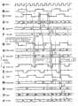
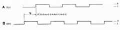
在图4(以及图5)中,A、B、C……I是DQS域,J、K、L......P是I CLK域。为了便于说明,使用图4作为代表图来进行说明。In Figure 4 (and Figure 5), A, B, C...I is the DQS domain, J, K, L...P is the I CLK domain. For convenience of description, FIG. 4 will be used as a representative diagram for description.
鉴于此,时钟发生器34如图4的A所示被施加CLK信号,在存储器4的输出缓冲器22中如图4的B所示获得DQS信号,在存储器4的输出缓冲器24中获得DQ信号。该DQ信号如图4的D所示,由数据d00、d01、d02、d03、d04、d05、d06、d07、d10、d11、d12、d13......构成。In view of this, the
在DL44的输出侧如图4的C所示,获得使DQS信号位移了90度相位的信号dqs90。与之对应,在FF52的输出侧如图4的E所示,获得从DQ信号得到的信号dq_even,在FF54的输出侧如图4的F所示,获得从DQ信号得到的信号dq_odd。信号dq_even由数据d00、d02、d04、d06、d10......构成。另外,信号dq_odd由数据d01、d03、d05、d07、d11......构成。On the output side of DL44, as shown in C of FIG. 4, a signal dqs90 in which the phase of the DQS signal is shifted by 90 degrees is obtained. Correspondingly, on the output side of FF52, as shown in E of FIG. 4, the signal dq_even obtained from the DQ signal is obtained, and on the output side of FF54, as shown in F of FIG. 4, the signal dq_odd obtained from the DQ signal is obtained. The signal dq_even is composed of data d00, d02, d04, d06, d10, . . . . In addition, the signal dq_odd is composed of data d01, d03, d05, d07, d11, . . . .
在DL60的输出侧如图4的G所示,获得使DQS信号延迟后的信号ddqs。与之对应,在DL62的输出侧如图4的H所示,获得使DQ信号延迟后的信号ddq_even,在DL64的输出侧如图4的I所示,获得使DQ信号延迟后的信号ddq_odd。信ddq_even号由数据d00、d02、d04、d06、d10......构成。另外,信号ddq_odd由数据d01、d03、d05、d07、d11......构成。On the output side of DL60, as shown in G of FIG. 4 , a signal ddqs obtained by delaying the DQS signal is obtained. Correspondingly, at the output side of DL62, as shown in H in FIG. 4 , a signal ddq_even after delaying the DQ signal is obtained, and at the output side of DL64, as shown at I in FIG. 4 , a signal ddq_odd after delaying the DQ signal is obtained. The signal ddq_even number is composed of data d00, d02, d04, d06, d10.... In addition, the signal ddq_odd is composed of data d01, d03, d05, d07, d11, . . . .
在时钟发生器34中,如图4的J所示获得从CLK信号得到的信号even_en。另外,在反相器70的输出侧如图4的K所示,获得从CLK信号得到的信号odd_en。与之对应,在FF66的输出侧如图4的M所示,获得信号Idq_even,在FF68的输出侧如图4的N所示,获得信号Idq_odd。Idq_even由数据d00、d02、d04、d06、d10......构成。另外,信号Idq_odd由数据d01、d03、d05、d07、d11......构成。In the
如图4的L所示,选择器31被从时钟发生器34赋予选择控制信号sel(CLK信号)。与之对应,如图4的O所示,在选择器31中获得信号dqo。该信号dqo由数据d00、d01、d02、d03、d04、d05、d06、d07、d10......构成。As shown by L in FIG. 4 , the
而且,在FF74的输出侧如图4的P所示,获得输出数据信号ODQ。该输出数据信号ODQ由数据d00、d01、d02、d03、d04、d05、d06、d07......构成。Also, on the output side of the
在该定时图中,在处理(a)中使DQS信号的相位延迟90度。该情况下,对应于DQS信号(图4的B)的正沿(从L电平向H电平迁移的电平),生成信号dqs90(图4的C)的负沿(从H电平向L电平迁移的电平)。与之对应,执行处理(c)(图4的G、H、I、J)。In this timing chart, the phase of the DQS signal is delayed by 90 degrees in the process (a). In this case, the negative edge (from H level to H level) of signal dqs90 (C in FIG. L level shifted level). Accordingly, processing (c) is executed (G, H, I, J in FIG. 4 ).
在处理(b)中,在使相位延迟90度后的DQS信号(dqs90)的上升沿、下降沿获取DQ信号。对应于信号dqs90(图4的C)的正沿、DQ信号(图4的D)的d02,基于处理(b)的执行获得信号dq_even(图4的E)的数据d02。与之对应,作为处理(d),获得信号ddq_even(图4的H)的数据d02。In the process (b), the DQ signal is acquired at the rising and falling edges of the DQS signal ( dqs90 ) whose phase is delayed by 90 degrees. Corresponding to the positive edge of the signal dqs90 (C of FIG. 4 ), d02 of the DQ signal (D of FIG. 4 ), data d02 of the signal dq_even (E of FIG. 4 ) is obtained based on execution of the process (b). Correspondingly, as the process (d), data d02 of the signal ddq_even (H in FIG. 4 ) is obtained.
处理(c)由延迟控制部12执行,在该处理(c)中,对延迟与定时进行调整,以便使DQS信号延迟后的信号ddqs(图4的G)的下降、与CLK信号(相当500〔MHz〕)的下降的定时一致。当信号ddqs的下降为even_en=L时,基于相位检测部10的输出对DL60的延迟量进行控制,以便与CLK信号的下降沿一致。The process (c) is executed by the
处理(d)对DQ信号(ddq_even,ddq_odd)赋予和处理(c)相同的延迟。对应于信号dqs90(图4的C)的负沿、DQ信号(图4的D)的数据d03,基于处理(b)的执行获得信号dq_odd(图4的F)的数据d03。与之对应,在处理(d)中,通过CLK信号获取DQ信号(ddq_even,ddq_odd)。即,在处理(d)中获得信号ddq_odd(图4的I)的数据d03。In the process (d), the same delay as in the process (c) is given to the DQ signal (ddq_even, ddq_odd). Corresponding to the negative edge of the signal dqs90 (C of FIG. 4 ), data d03 of the DQ signal (D of FIG. 4 ), data d03 of the signal dq_odd (F of FIG. 4 ) is obtained based on execution of the process (b). Correspondingly, in the process (d), the DQ signals (ddq_even, ddq_odd) are acquired through the CLK signal. That is, the data d03 of the signal ddq_odd (I of FIG. 4 ) is obtained in the process (d).
处理(e)通过CLK信号获取延迟后的DQ信号(ddq_even,ddq_odd)(即,是CLK信号的切换)。基于信号ddq_even(图4的H)的数据d02,得到信号Idq_even(图4的M)的数据d02。根据信号ddq_odd(图4的I)的数据d03,得到信号Idq_odd(图4的N)的数据d03。即,通过图4的H、I、J、K的处理,对DQS信号执行CLK信号的转换。Processing (e) acquires the delayed DQ signal (ddq_even, ddq_odd) through the CLK signal (that is, switching of the CLK signal). Based on the data d02 of the signal ddq_even (H in FIG. 4 ), the data d02 of the signal Idq_even (M in FIG. 4 ) is obtained. From the data d03 of the signal ddq_odd (I in FIG. 4 ), the data d03 of the signal Idq_odd (N in FIG. 4 ) is obtained. That is, through the processing of H, I, J, and K in FIG. 4 , conversion of the CLK signal is performed on the DQS signal.
处理(f)将通过CLK信号获取的DQ信号(ldq_even,ldq_odd)进行多路复用,使其1〔Gbps〕化。基于信号Idq even(图4的M)的数据d02得到信号dqo(图4的O)的数据d02,对应于该数据d02,得到输出数据信号ODQ(图4的P)的数据d02。The process (f) multiplexes the DQ signals (ldq_even, ldq_odd) acquired by the CLK signal to 1 [Gbps]. Based on the data d02 of the signal Idq even (M in FIG. 4 ), the data d02 of the signal dqo (O in FIG. 4 ) is obtained, and corresponding to the data d02, the data d02 of the output data signal ODQ (P in FIG. 4 ) is obtained.
接下来,参照图6对基于DQS信号的DQ信号的获取进行说明。图6是表示接收DQS信号以及DQ信号的定时的图。Next, acquisition of a DQ signal based on a DQS signal will be described with reference to FIG. 6 . FIG. 6 is a diagram showing timings at which a DQS signal and a DQ signal are received.
在从存储器4{例如DDR3存储器(DIMM)}读出数据的情况下,存储器4根据从信号接收电路2接收到的CK信号生成DQS信号。将与该DQS信号同步的DQ信号以DDR(Double Data Rate)输出。DQS信号与DQ信号的相位关系如图6的A以及C所示,DQS信号的变化与DQ信号的变化为同相位。因此,在信号接收电路2侧,由DL44使DQS信号延迟tCK/4(图6的B),使DQS信号的变化点位移到DQ信号的变化的中央。图6的B是位移了tCK/4后的DQS信号(图6的A)。由此,使用DQS信号的两个沿,将DQ信号向信号接收电路2侧取入。In the case of reading data from the memory 4 {eg, DDR3 memory (DIMM)}, the
接下来,参照图7对DQ信号向内部时钟相位的切换进行说明。图7是用于对相位控制进行说明的图。Next, switching of the DQ signal to the internal clock phase will be described with reference to FIG. 7 . FIG. 7 is a diagram for explaining phase control.
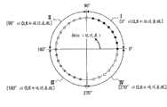
在信号接收电路2中,将接收到的DQS信号与相位检测器58的4相CLK信号中的一个进行相位比较,求出相位差。由DL60实施延迟处理,以使该相位一致。该DL60进行的延迟由相位检测部10的相位差决定(DQPHASE)信号决定。相位检测器58基于DQPHASE信号将4相CLK信号中的一个与延迟后的DQS信号的相位进行比较,并调整延迟量(=DQPHASE),以使DQS信号的相位与CLK信号的相位相符。In the
该情况下,在DQS信号比CLK信号延迟的情况下,朝向减少延迟量(DQPHASE)的方向进行控制,另外,在DQS信号比CLK信号超前的情况下,朝向增多延迟量(DQPHASE)的方向进行控制。In this case, when the DQS signal is delayed from the CLK signal, control is performed to reduce the delay amount (DQPHASE), and when the DQS signal is ahead of the CLK signal, control is performed to increase the delay amount (DQPHASE). control.
在DL60中,相位的最大延迟量小于tCK/4(=4相CLK信号的相间延迟差)。鉴于此,当需要DL60的最大延迟量以上的延迟时,在使4相CLK信号的选择位移到早1个相量的CLK信号之后,使DL60的延迟量最小,再次进行相位比较。并且,为了获得大的延迟,只要再次增大DL60的延迟量即可。In DL60, the maximum delay of the phase is less than tCK/4 (= phase-to-phase delay difference of 4-phase CLK signals). In view of this, when a delay greater than the maximum delay of DL60 is required, after shifting the selection of the 4-phase CLK signal to a CLK signal one phase earlier, the delay of DL60 is minimized, and the phase comparison is performed again. And, in order to obtain a large delay, it is only necessary to increase the delay amount of DL60 again.
该情况下,当DL60的延迟量再次达到了最大延迟量(可变延迟量的极限)时,只要使4相CLK信号的选择变化成更早1个相量的CLK信号即可。总之,重复小于DL60的最大延迟量的延迟、和基于4相CLK信号的早1个相量的CLK信号的位移的延迟控制。In this case, when the delay amount of DL60 reaches the maximum delay amount (the limit of the variable delay amount) again, it is only necessary to change the selection of the 4-phase CLK signal to the CLK signal one phasor earlier. In short, a delay smaller than the maximum delay amount of DL60 and a delay control based on a shift of the CLK signal one phasor earlier than the four-phase CLK signal are repeated.
在该延迟控制中,例如若当前延迟差为40度,则以0度相位的CLK信号、和40度相位量的延迟进行相位延迟。若延迟逐渐变大,则只要增大DL60的延迟量即可。该情况下,若延迟变为90度,则由于在DL60中无法实现该延迟,所以将CLK信号切换成270(-90)度,该情况下,只要将DL60的延迟设为0即可。鉴于此,在图7中表示了区域I是延迟为0度以上小于90度的范围(黑圆圈),区域II是延迟为90度以上小于180度的范围(斑点圆圈),区域III是延迟为180度以上小于270度的范围(斜线圆圈),区域IV是延迟为270度以上小于360度(0度)的范围(白圆圈)的控制。In this delay control, for example, if the current delay difference is 40 degrees, the phase delay is performed by using the CLK signal with a phase of 0 degrees and a phase delay of 40 degrees. If the delay becomes larger gradually, it only needs to increase the delay amount of DL60. In this case, if the delay becomes 90 degrees, the delay cannot be realized by DL60, so the CLK signal is switched to 270 (−90) degrees. In this case, the delay of DL60 should be set to 0. In view of this, in Figure 7, it is shown that the area I is the range (black circle) with a delay of 0 degrees or more and less than 90 degrees, the area II is the range with a delay of 90 degrees or more and less than 180 degrees (spotted circle), and the area III is the delay of The range above 180 degrees and less than 270 degrees (hatched circle), and area IV is the control where the delay is in the range of more than 270 degrees and less than 360 degrees (0 degrees) (white circle).
接下来,参照图8对4相CLK信号的生成进行说明。图8是表示4相CLK信号的生成的定时图。Next, generation of the 4-phase CLK signal will be described with reference to FIG. 8 . FIG. 8 is a timing chart showing generation of 4-phase CLK signals.
4相CLK信号由时钟发生器34根据基准CLK信号生成。在时钟发生器34由分频电路构成的情况下,如图8的A所示,当被赋予CLK信号时,对该CLK信号进行分频,如图8的B所示,生成相位差0度的CLK信号。以该相位差0度的CLK信号为基准,生成具有规定相位差的图8的C、D、E所示的CLK信号。图8的C是从相位差0度的CLK信号延迟了时间T1后的相位差90度的CLK信号。图8的D是从相位差0度的CLK信号延迟了时间T2后的相位差180度的CLK信号。图8的E是从相位差0度的CLK信号延迟了时间T3后的相位差270度的CLK信号。The 4-phase CLK signal is generated by the
接下来,参照图9、图10、图11以及图12对相位检测部10进行说明。图9是表示相位检测部的一个例子的图,图10是表示相位比较部的一个例子的图,图11表示相位检测动作,图12是表示相位比较的逻辑动作以及输出状态的图。Next, the
相位检测部10如上所述,具备S/H电路56和相位检测器58。S/H电路56如图9所示,接收被DL60延迟后的DQS信号,如果将该DQS信号设为信号a,则生成同等的信号a’、和从信号a使相位稍微延迟(微小延迟)的信号b。相位检测器58使用相位不同的两个信号a’、b来检测CLK信号的相位。The
相位检测器58中设置有相位比较部80。该相位比较部80如图10所示,设置有第1FF82、第2FF84。各FF82、84被共通施加CLK信号,并对一方的FF82施加了信号a’,对另一方的FF84施加了信号b。A
对于各DQS信号、信号a’、b以及CLK信号而言,相对于第11图的A所示的DQS信号,在信号a’中如第11图的B所示产生基于DL60的延迟tDL。另外,相对于信号a’,信号b如第11图的C所示那样产生了微小延迟tSH。虚线rt是比较基准位置。For each DQS signal, signals a', b, and CLK signal, a delay tDL by DL60 occurs in signal a' as shown in B in FIG. 11 with respect to the DQS signal shown in A in FIG. 11 . In addition, the signal b has a slight delay tSH with respect to the signal a' as shown in C in FIG. 11 . The dotted line rt is a comparison reference position.
如果这样的DQS信号、信号a’、b以及CLK信号被施加给相位比较部80,则在FF82的输出FFO1、FF84的输出FFO2中如图12所示,得到相位的延迟信息。When such a DQS signal, signals a', b, and CLK signal are applied to the
关于该相位的延迟信息,1)在输出FFO1=L、FFO2=L的情况下,延迟过多(使DQS的相位提前)。2)在输出FFO1=L、FFO2=H的情况下,延迟相反180度。3)在输出FFO1=H、FFO2=L的情况下,延迟适当(OK)。4)在输出FFO1=H、FFO2=H的情况下,延迟不足(使DQS的相位滞后)。Regarding the delay information of this phase, 1) In the case of outputting FFO1=L and FFO2=L, the delay is excessive (the phase of DQS is advanced). 2) In the case of outputting FFO1=L and FFO2=H, the delay is reversed by 180 degrees. 3) When outputting FFO1=H and FFO2=L, the delay is appropriate (OK). 4) In the case of output FFO1=H, FFO2=H, the delay is insufficient (the phase of DQS is delayed).
接下来,参照图13、图14以及图15对相位检测部10进行说明。图13是表示相位检测部的一个例子的图,图14是表示延迟信息的图,图15是用延迟信息表示了相位的图。在图13中,对与图3、图9相同的部分赋予了相同的附图标记。Next, the
相位检测部10中如图13所示,具备S/H电路56以及相位检测器58。相位检测器58具备已叙述的相位比较部80、第1计数器86以及第2计数器88。As shown in FIG. 13 , the
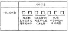
S/H电路56根据由DL60获得的信号a(=DQS信号)生成信号a’、b。相位比较部80将CLK信号与信号a’、b进行比较,获得输出FFO1、FFO2(图10、图12)。各输出FFO1、FFO2如图13所示,构成相位的延迟信息。该延迟信息例如可以如图14所示,用7〔比特〕的数字信息(即7位的2进数)表示。The S/
在该延迟信息中,下3位(3〔比特〕)是针对DL60的延迟控制信息,在该实施方式中,是小于90度的延迟调整信息。中2位(2〔比特〕)是针对时钟生成部14的CLK选择信息,在该实施方式中,是以规定相位差90度为单位的延迟量选择信息。另外,上2位(2〔比特〕)表示第几周期的相位、即其周期次数。是针对时钟生成部14的时钟选择信息,在该实施方式中,是以规定相位差90度为单位的延迟量选择信息。In this delay information, the lower 3 bits (3 [bits]) are delay control information for
鉴于此,在该相位控制中,S/H电路56生成对DQS信号附加了微小的延迟而得到的信号a进而附加了微小的延迟的信号b。相位检测器58基于信号a’、b与CLK信号的比较来判定DQS信号的相位。计数器86是根据相位比较部80的相位检测的输出来对检测出的相位信号进行积分的单元。该相位信号的积分用于防止误动作。In view of this, in this phase control, the S/
鉴于此,计数器86对相位信号(相位比较部80的输出)进行计数,其计数值被施加给计数器88。如果计数器86的计数值超过了预先决定的规定值(阈值),则与之对应使计数器88的计数值增加或者减少,将计数器86的计数值复位。存在计数器86的计数值在正侧超过已叙述的阈值的情况、和在负侧超过已叙述的阈值的情况。当其计数值在正侧超过已叙述的阈值时,使计数器88的计数值增加。另外,当其计数值在负侧超过已叙述的阈值时,使计数器88的计数值减少。In view of this, the
计数器88的输出是延迟信息(图14),该延迟信息被用于DL60的延迟控制、时钟生成部14的CLK选择即相位变更。The output of the
该延迟信息如图14所示,是任意比特(bit)长的数字量,将其初始值例如设为“0000000”。鉴于此,在DL60中,使用该延迟信息中的下位3〔比特〕来决定自身的通过延迟。在该实施方式中,实现了将90度相位8等分中的一个延迟(0~7/8×90度)。如图15所示,是圆周的黑圆圈、斑点圆圈、斜线圆圈、白圆圈的角度。在图15中,是以延迟信息表现了相位的例子。As shown in FIG. 14 , this delay information is a digital quantity with an arbitrary bit (bit) length, and its initial value is set to “0000000”, for example. In view of this, in the DL60, the lower 3 [bits] of the delay information are used to determine its own transit delay. In this embodiment, one delay (0 to 7/8×90 degrees) in which the 90-degree phase is divided into eight equal parts is realized. As shown in Fig. 15, it is the angle of the black circle, the spot circle, the slash circle, and the white circle of the circumference. In FIG. 15, the phase is represented by delay information.
该情况下,由于将1周的360度32等分来表现,所以在图15中,第一象限(I)的延迟信息为xx00xxx。第二象限(II)的延迟信息为xx01xxx。第三象限(III)的延迟信息为xx10xxx。第四象限(IV)的延迟信息为xx11xxx。而且,在延迟为n周的情况下,下5〔比特〕相同。In this case, since 360 degrees and 32 equal parts of one cycle are expressed, in FIG. 15 , the delay information of the first quadrant (I) is xx00xxx. The delay information for the second quadrant (II) is xx01xxx. The delay information for the third quadrant (III) is xx10xxx. The delay information for the fourth quadrant (IV) is xx11xxx. Also, when the delay is n weeks, the lower 5 [bits] are the same.
鉴于此,CLK信号的选择使用延迟信息中下位第5〔比特〕以及第4〔比特〕(即中位2〔比特〕),选择了具有应该选择的相位的CLK信号。In view of this, the selection of the CLK signal uses the lower 5 [bit] and 4 [bit] (that is, the middle 2 [bit]) in the delay information, and selects the CLK signal with the phase that should be selected.
这里,如果对DL60例如使用延迟线、且其长度无限,则能够仅由该DL60进行相位调整,但这是不可能的。现实中其长度是有限的,无法只通过该延迟电路来进行相位调整。并且,虽然通过延迟电路能够附加延迟,但无法进行负延迟。Here, if a delay line is used for DL60, for example, and its length is infinite, phase adjustment can be performed only by this DL60, but this is impossible. In reality, its length is limited, and phase adjustment cannot be performed only through this delay circuit. Also, although a delay can be added by a delay circuit, negative delay cannot be performed.
鉴于此,当在相位调整中以将90度8等分(将360度32等分)的精度进行延迟调整时,相位延迟信息(图14)的下位3〔比特〕成为小于90度的调整量。该情况下,中位2〔比特〕是在90度单位中使用哪个相位的信息,将其用于对具有以90度为单位的相位延迟的CLK信号的选择。另外,上位2〔比特〕成为表示是第几周期相位的信号。而且,该电路的相位跟踪范围通过用哪个〔比特〕表示该延迟信息来决定。In view of this, when the delay adjustment is performed with the accuracy of dividing 90 degrees into 8 equal parts (360 degrees into 32 equal parts), the lower 3 [bits] of the phase delay information (Figure 14) become an adjustment amount smaller than 90 degrees . In this case, the middle bit 2 [bit] is information on which phase is used in units of 90 degrees, and is used to select a CLK signal having a phase delay in units of 90 degrees. In addition, the upper 2 [bits] are a signal indicating which cycle phase it is. Also, the phase tracking range of the circuit is determined by which [bit] is used to represent the delay information.
这样,在该相位调整中,通过并用基于DL60的延迟调整、与基于CLK信号的相位选择,增大了DQ信号的相位调整的自由度。即,设想实现了相位的负延迟、过大的相位延迟双方。因此,与仅通过DL60进行延迟调整的情况相比,具有以下优点。As described above, in this phase adjustment, the degree of freedom of phase adjustment of the DQ signal is increased by using delay adjustment by DL60 and phase selection by CLK signal in combination. That is, it is assumed that both negative phase delay and excessive phase delay are realized. Therefore, compared with the case where the delay adjustment is performed only by the DL60, there are the following advantages.
a)虽然DL60与延迟量成比例增大,但在使用了CLK信号选择的上述构成中,可减小整体的电路规模。a) Although DL60 increases in proportion to the amount of delay, the overall circuit scale can be reduced in the above configuration using CLK signal selection.
b)仅通过增加计数器86、88的比特数,便能够应对十分大的范围(理论上无限大)的延迟。b) By only increasing the number of bits of the
c)还可以应对负延迟。在仅通过DL60实现的情况下,需要附上预料到最小值的补偿(offset)延迟,但在使用了CLK信号选择的上述构成中,不需要这样的补偿延迟。c) Can also handle negative latencies. In the case of realizing only by DL60, it is necessary to add an offset (offset) delay of an expected minimum value, but such an offset delay is not required in the above configuration using CLK signal selection.
接下来,参照图16、图17、图18以及图19对时钟切换进行说明。图16是用于对时钟转换动作进行说明的图,图17、图18以及图19是表示时钟转换动作的一个例子的定时图。在图16中,对与图3相同的部分赋予了相同的附图标记。Next, clock switching will be described with reference to FIGS. 16 , 17 , 18 and 19 . FIG. 16 is a diagram for explaining the clock switching operation, and FIGS. 17 , 18 and 19 are timing charts showing an example of the clock switching operation. In FIG. 16 , the same reference numerals are given to the same parts as those in FIG. 3 .
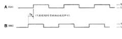
在相位控制部8中,为了说明时钟切换,如图16所示,与已叙述的相位检测部10、延迟控制部12的相位延迟部16、18一起提取出相位设定部30。即,表示了从信号接收电路2提取出相位检测部10,从相位设定部30提取出FF52,从相位延迟部16提取出DL60、62,从相位延迟部18提取出FF66。In the
该情况下,在从FF52向FF66传播DQ信号(数据)时,DQS信号的相位发生偏差。针对该相位差别,DL60使用FF52的CLK(DQS)与FF66(CLK)的相位关系来进行相位延迟(延迟增补),但由此DL60、62变大,因此无法实现太大的延迟。鉴于此,除了基于DL60、62的相位调整之外,还通过变更在FF66侧设定的CLK信号的相位,来进行时钟切换用的相位控制。即,在相位差超过90度的情况下,以90度的相位为单位变更CLK信号的相位,在小于90度的情况下,由DL60进行相位调整。该情况下,90度单位的相位调整将CLK信号向反方向(使相位超前的方向)控制,在想要等效地增大延迟量的值时,提前了CLK信号的相位。In this case, when the DQ signal (data) propagates from FF52 to FF66, the phase of the DQS signal deviates. For this phase difference, DL60 uses the phase relationship between FF52's CLK (DQS) and FF66 (CLK) to perform phase delay (delay supplementation). However, since DL60 and 62 become larger, a large delay cannot be realized. In view of this, in addition to phase adjustment by DL60 and 62, phase control for clock switching is performed by changing the phase of the CLK signal set on the FF66 side. That is, when the phase difference exceeds 90 degrees, the phase of the CLK signal is changed in units of a 90-degree phase, and when it is less than 90 degrees, the phase adjustment is performed by the
关于该相位调整,图17是DQS信号(图17的B)的相位比CLK信号(图17的A)稍微(小于90度)前进的情况。该情况下,只要使用DL60并根据DQS信号与CLK信号的相位差Ta(<90度)使DQS信号的相位延迟即可。该情况下,通过DL62对DQ信号同样地进行相位调整。Regarding this phase adjustment, FIG. 17 shows a case where the phase of the DQS signal (B in FIG. 17 ) advances slightly (less than 90 degrees) than the phase of the CLK signal (A in FIG. 17 ). In this case, it is only necessary to use DL60 to delay the phase of the DQS signal according to the phase difference Ta (<90 degrees) between the DQS signal and the CLK signal. In this case, the DQ signal is similarly phase-adjusted by DL62.
如图18所示,在DQS信号(图18的B)的相位比CLK信号(图18的A)大幅(相位差Tb>90度)超前的情况下,需要使DQS信号的相位大幅延迟。该情况下,并用DL60的延迟和CLK信号的选择。As shown in FIG. 18 , when the phase of the DQS signal (B in FIG. 18 ) is significantly ahead of the CLK signal (A in FIG. 18 ) (phase difference Tb>90 degrees), it is necessary to greatly delay the phase of the DQS signal. In this case, use the delay of DL60 and the selection of CLK signal.
该情况下,如图19所示,如果将CLK信号(图19的A)的相位切换成超前了90度的CLK信号,则成为该CLK信号(图19的A)与DQS信号(图19的B)的相位稍微错开的状态。如果其相位差Tc小于90度(Tc<90度),则只要使用DL60,根据该相位差Tc使DQS信号的相位延迟即可。该情况下,DQ信号被进行CLK信号的变更和基于DL62的相位调整。其结果,进行针对相位延迟的相位控制,可使数据信号的定时最佳化。In this case, as shown in FIG. 19, if the phase of the CLK signal (A in FIG. 19) is switched to a CLK signal advanced by 90 degrees, the CLK signal (A in FIG. 19) and the DQS signal (A in FIG. B) A state where the phases are slightly shifted. If the phase difference Tc is less than 90 degrees (Tc<90 degrees), it is only necessary to use the DL60 to delay the phase of the DQS signal according to the phase difference Tc. In this case, the DQ signal is subjected to change of the CLK signal and phase adjustment by DL62. As a result, phase control for phase delay is performed, and the timing of the data signal can be optimized.
若对上述实施方式列举特征事项、优点,则如下所述。Listing the characteristic items and advantages of the above-mentioned embodiment, they will be as follows.
(1)在上述实施方式中,存储器控制器6的信号接收电路2包括相位检测部10和延迟控制部12。延迟控制部12具备时钟发生器34,根据CLK信号生成了具有规定相位差的4相CLK信号作为多相的CLK信号。相位检测部10中具备将由存储器4生成的DQS信号、与被实施了延迟处理的CLK信号进行比较来求出相位差的相位检测器58。(1) In the above-described embodiment, the
(2)在上述实施方式中,可以基于DL60的延迟量、和基于从4相CLK信号选择的CLK信号的相位选择,来使延迟跟踪信号变化。具体而言,可以根据生成并存储延迟信息(DQPHASE)的计数器86、88的比特数来使延迟跟踪信号变化。(2) In the above-described embodiment, the delay tracking signal can be changed based on the delay amount of the
(3)在减少延迟量的情况下,减小DL60的延迟量,不能得到其延迟小于0的延迟。该情况下,通过从4相CLK信号选择早1个相量的CLK信号,使DL60的延迟量最大(=4相CLK信号的相间延迟差),可获得同样的效果。(3) In the case of reducing the delay amount, the delay amount of DL60 is reduced, and a delay whose delay is less than 0 cannot be obtained. In this case, the same effect can be obtained by selecting a CLK signal one phasor earlier from the 4-phase CLK signals to maximize the delay amount of the DL60 (= phase delay difference of the 4-phase CLK signals).
(4)因此,在信号接收电路2中,能够一边将DQS信号的变化相位、和信号接收电路2中的时钟相位保持为最佳状态,一边将DQ信号(数据)从DQS相位转换成内部时钟相位。并且,可获得相位差转换所需要的延迟量(=相位差量)作为延迟信息,并将其输出。(4) Therefore, in the
(5)在该信号接收电路2中,只要是用延迟用的缓冲器(8/32tck)和生成4个相位不同的波长的时钟发生器34即可。另外,在该信号接收电路2中,能够应对与来自存储器4的DQ信号的高速化相伴的、到达时间的偏差(例如因温度等引起的偏差),可以将延迟时间等延迟信息通知给处理器等上位电路。在上述电路中,可将该延迟信息用于存储器控制器6的设计、控制等。另外,由于使用时钟发生器34,所以能够通过小的缓冲器来测定延迟时间。(5) In the
(6)信号接收电路2具备相位检测部10以及延迟控制部12作为相位控制部8,相位检测部10具备将输入数据的相位基准信号(DQS)与内部基准时钟进行比较的相位比较部80。相位检测部10通过与CLK信号的比较来决定并输出DQS信号的延迟量(DQPHASE)。在相位延迟部16中,具备DL60作为接收相位检测部10的输出信号,对输入数据的相位基准信号(DQS)的延迟量进行改变的可变延迟单元。另外,在相位延迟部16中,具备DL62、64作为接收相位检测部10的输出信号,对接收数据的延迟量进行改变的可变延迟单元。另外,延迟控制部12中具备时钟生成部14,该时钟生成部14接收相位检测部10的输出信号,切换分频输出的相位。具体而言,时钟发生器34例如由分频器构成,生成4相的CLK信号。具备选择器36作为该CLK信号的选择单元,从相位检测部10对该选择器36施加延迟信息作为选择信息。其结果,选择器36从4相的CLK信号中选择适合延迟量的CLK信号,输出该CLK信号。而且,信号接收电路2中具备数据保持部32,该数据保持部32例如由FF74构成,获取并保持信号接收电路2的输出数据。(6) The
(7)S/H电路56也可以由可变延迟器构成。(7) The S/
(8)延迟量(DQPHASE)被作为数字量输出。(8) The delay quantity (DQPHASE) is output as a digital quantity.
(9)时钟发生器34由分频器构成,对该分频器设定的分频比(CKGEN)被设定为2n(其中,n为1或者2以上的自然数)。(9) The
(10)可以取代延迟电路而由相位延迟电路构成DL44、50、60、62、64。(10) The
〔第3实施方式〕[Third embodiment]
第3实施方式使用了第1延迟信息(dqphase1)和第2延迟信息(dqphase2)作为根据相位差得到的延迟信息(DQPHASE)。该情况下,第1延迟信息是以规定相位差为单位的延迟量,是将相位基准信号的相位例如以90度单位变更的延迟量。另外,第2延迟信息是用于在不超过以规定相位差为单位的延迟量的范围使相位基准信号的相位延迟的延迟量。The third embodiment uses first delay information (dqphase1) and second delay information (dqphase2) as delay information (DQPHASE) obtained from a phase difference. In this case, the first delay information is a delay amount in units of a predetermined phase difference, and is a delay amount in which the phase of the phase reference signal is changed, for example, in units of 90 degrees. In addition, the second delay information is a delay amount for delaying the phase of the phase reference signal within a range not exceeding the delay amount in units of a predetermined phase difference.
参照图20对该第3实施方式进行说明。图20是表示第3实施方式涉及的信号接收电路的一个例子的图。在图20中,对与图3相同的部分赋予了相同的附图标记。This third embodiment will be described with reference to FIG. 20 . FIG. 20 is a diagram showing an example of a signal receiving circuit according to the third embodiment. In FIG. 20 , the same reference numerals are assigned to the same parts as in FIG. 3 .
该实施方式的相位检测部10与上述实施方式相同,具备S/H电路56和相位检测器58。由于S/H电路56与上述实施方式相同,所以省略其说明。The
另外,相位检测器58获得第1延迟信息dqphase1和第2延迟信息dqphase2作为延迟信息(DQPHASE)。该情况下,dqphase1是已叙述的延迟信息(图14)的上位4〔比特〕量的信息,dqphase2是已叙述的延迟信息(图14)的下位3〔比特〕量的信息。Also, the
在该构成中,延迟信息dqphase1被向时钟生成部14侧传递。由此,时钟生成部14输出具有与延迟信息对应的延迟量的CLK信号。该情况下,相位检测器58以及FF66被从时钟生成部14施加同相的CLK信号,FF68被施加其反转的CLK信号。同样,从时钟生成部14对选择器31施加选择控制信号。另外,dqphas2被赋予给DL60、62、64。In this configuration, the delay information dqphase1 is passed to the
根据这样的构成,也能够和第2实施方式同样地进行针对与相位差对应的DQS信号、DQ信号的相位延迟。而且,由于各部分的动作波形与第2实施方式(图3、图4及图5)相同,所以将对图3附加的符号附加给图20。由于详细的说明如第2实施方式中叙述那样,所以省略说明。According to such a configuration, it is also possible to perform phase delays for DQS signals and DQ signals corresponding to phase differences in the same manner as in the second embodiment. In addition, since the operation waveforms of each part are the same as those of the second embodiment ( FIGS. 3 , 4 , and 5 ), the symbols assigned to FIG. 3 are assigned to FIG. 20 . Since the detailed description is the same as that described in the second embodiment, the description is omitted.
〔其他实施方式〕[Other Embodiments]
(1)在上述实施方式中,例示了设置于存储器控制器6的信号接收电路2作为信号接收电路,但本申请公开的信号接收电路并不限定于上述实施方式。例如,本申请公开的信号接收电路可以在存储器控制器6等存储器接口电路以外使用,用于接收伴随相位变动的信号。(1) In the above-mentioned embodiment, the
(2)在上述实施方式中,对存储器控制器6进行了描述,但本申请公开的存储器控制器并不限定于上述实施方式。例如,也可以使用本申请公开的存储器控制器构成处理器100(图21),还可以构成计算机200(图22)。(2) In the above embodiment, the
(3)处理器100例如构成为CPU(Central Processing Unit)、MPU(Micro Processor Unit)。如图21所示,该处理器100也可以将对存储器4的数据传输进行控制的存储器控制器6、和执行运算处理等的单元的运算处理部102并列设置。该情况下,可以在存储器控制器6中构成已叙述的信号接收电路2。根据该构成,也能获得上述实施方式中的效果,可实现数据传输的高速化,提高可靠性。(3) The
(4)计算机200也可以如图22所示,在设置于CPU202和存储器4之间的芯片组204的内部具备存储器控制器6。该情况下,可以在存储器控制器6中构成已叙述的信号接收电路2。根据该构成,也能获得上述实施方式中的效果,可实现数据传输的高速化,提高可靠性。(4) As shown in FIG. 22 , the
(5)也可以成为在CPU202的内部具备存储器控制器6,在该存储器控制器6的内部具备已叙述的信号接收电路2的构成。根据该构成,也能获得上述实施方式中的效果,可实现数据传输的高速化,提高可靠性。(5) A
(6)在上述实施方式中,将作为基准的内部时钟信号的频率设定为2〔GHz〕,使用了将相位比较用的时钟信号分频为500〔MHz〕频率的时钟信号,但并不限定于此。所设定的时钟信号的频率是任意的,上述实施方式中记载的数值只是一个例子。(6) In the above-mentioned embodiment, the frequency of the reference internal clock signal is set to 2 [GHz], and the clock signal obtained by dividing the frequency of the clock signal for phase comparison to 500 [MHz] is used. Limited to this. The frequency of the clock signal to be set is arbitrary, and the numerical values described in the above-mentioned embodiments are merely examples.
(7)在上述第1实施方式所记载的相位控制的处理步骤(图2)中,也可以包括以上述延迟量为单位,生成具有相位差的多个时钟信号的步骤,根据上述相位差来选择上述时钟信号。并且,可以包括执行下述功能的步骤:将被第二相位延迟部18相位延迟后的输出数据保持到数据保持部32中。(7) The phase control processing procedure ( FIG. 2 ) described in the first embodiment may include a step of generating a plurality of clock signals with a phase difference in units of the above-mentioned delay amount, and generating clock signals based on the above-mentioned phase difference. Select the above clock signal. Furthermore, a step of performing a function of holding the output data phase-delayed by the second
〔比较例〕[Comparative example]
比较例是伴随相位变动的信号的信号接收电路,是存储器控制器的信号接收电路的一个例子。The comparative example is a signal receiving circuit for a signal accompanied by a phase change, and is an example of a signal receiving circuit for a memory controller.
参照图23、图24、图25以及图26对该比较例进行说明。图23是表示存储器控制器的比较例的图,图24是表示电路的延迟偏差的试算例的图,图25是表示DIMM上的时钟布线方式的图,图26是表示DIMM上的其他时钟布线方式的图。This comparative example will be described with reference to FIGS. 23 , 24 , 25 and 26 . FIG. 23 is a diagram showing a comparative example of a memory controller, FIG. 24 is a diagram showing a trial calculation example of a circuit delay variation, FIG. 25 is a diagram showing a clock wiring method on a DIMM, and FIG. 26 is a diagram showing other clocks on a DIMM. Diagram of the wiring scheme.
为了最简单地从DIMM接收DDR信号,只要如图23所示那样构成存储器控制器600即可。存储器控制器600中设置有信号接收电路604作为从DIMM602接收信号的单元,该信号接收电路604中设置有时钟树部606作为赋予时钟信号的单元。时钟树部606以及信号接收电路604由LSI构成。In order to receive DDR signals from DIMMs most simply, it is only necessary to configure the
该情况下,信号接收电路604接收输入数据的相位发生变动的信号,构成DDR存储器接口电路的信号接收电路。该信号接收电路604中具备FF电路608、610、612、614、616、DL618、620、输出缓冲器622、输入缓冲器624、626。时钟树部606构成LSI内部时钟电路部,具备反相器628、630、632、634、636、638、640。DIMM602中具备输入缓冲器642、输出缓冲器644。In this case, the
鉴于此,信号接收电路604接收由时钟树部606生成的CLK信号,生成CK信号CK0并向DIMM602发送。DIMM602根据CK信号生成DQS信号,并与DQ信号一同反还给信号接收电路604。在信号接收电路604中,使用DQS信号对DQ信号进行重定时,进而转换成内部时钟。此时,为了利用接收点的锁存器可靠地接收数据,要求内部时钟与接收数据的定时关系处于一定的范围内。In view of this, the
如图24所示,在信号接收电路604中被认为延迟偏差的因素包括各种因素。假设全部考虑了这些因素的情况。该情况下,设想信号接收点是位于DL618的输出侧的FF610的输入部(图23)。即使传输路长度为0〔mm〕,如果以构成信号接收电路604的LSI内的接收点锁存器的时钟基准来看,则接收数据也具有982〔ps〕~4,156〔ps〕的延迟偏差。在该宽度(3,174〔ps〕)比时钟周期长,甚至比数据宽度长的(1〔GT/s〕传输时,数据宽度为1,000〔ps〕)。由于延迟偏差除了制造因素之外还包括环境因素(电源电压、装置温度),所以在运转中接收数据相位也不稳定(=跳动)。As shown in FIG. 24, factors considered to be delay deviations in the
然而,在DDR接口中如图25所示,针对构成DIMM602的存储器芯片651、652、653、654利用等长星型布线赋予了CK信号。与此相对,在DDR3接口中新采用了Flyby布线(图26)这一时钟布线手法。该Flyby布线如图26所示,针对DIMM602的存储器芯片651、652、653、654依次赋予CK信号。通过该Flyby布线,在信号的波形质量这一方面实现了改善。但是,数据收发信号定时在DQS组间不一致。因Flyby布线引起的时钟延迟的偏差最大预计为1000〔ps〕程度,该延迟与信号传输速度相比是无法忽视的大小。However, in the DDR interface, as shown in FIG. 25 , CK signals are given to the
关于数据发送时的CK信号与DQS信号的定时不一致,在JEDEC(Joint Electron Devices Engineering Council)标准中规定了其偏差吸收单元作为写入均衡(Write Leveling)。但是,没有与信号接收时的定时不一致有关的规定。Regarding the timing inconsistency between the CK signal and the DQS signal during data transmission, the JEDEC (Joint Electron Devices Engineering Council) standard specifies its deviation absorbing unit as write leveling (Write Leveling). However, there is no regulation regarding timing inconsistency at the time of signal reception.
本申请公开的存储器控制器、处理器、计算机或者相位控制方法提出了对DDR3接口等的已叙述的延迟偏差进行吸收的结构。在上述实施方式中,作为已叙述的课题的延迟被改善到与信号传输速度相比可以忽视的程度。The memory controller, processor, computer, or phase control method disclosed in the present application proposes a structure that absorbs the already described delay variation of the DDR3 interface or the like. In the above-described embodiments, the delay, which is the problem already described, is improved to a negligible level compared with the signal transmission speed.
如以上所述那样,本申请公开的信号接收电路、存储器控制器、处理器、计算机或者相位控制方法并不限定于上述记载。根据权利要求书记载、或者用于实施发明的方式中公开的主旨,本领域技术人员显然能够进行各种变形、变更。该变形、变更当然包含在本发明的范围中。As described above, the signal receiving circuit, memory controller, processor, computer, or phase control method disclosed in the present application are not limited to those described above. It is obvious to those skilled in the art that various deformation|transformation and changes can be made based on the subject matter disclosed in the claim description or the form for carrying out the invention. Such modifications and changes are of course included in the scope of the present invention.
工业上的可利用性Industrial availability
本申请公开的信号接收电路、存储器控制器、处理器、计算机或者相位控制方法针对信号接收抑制电路上的延迟偏差,提供实用性高的存储器控制器等,是有用的方案。The signal receiving circuit, memory controller, processor, computer, or phase control method disclosed in the present application is a useful solution for providing a memory controller with high practicability against delay variation in the signal receiving suppressing circuit.
附图标记的说明:2-信号接收电路;4-存储器;6-存储器控制器;10-相位检测部;12-延迟控制部;14-时钟生成部;16-第一相位延迟部;18-第二相位延迟部;58-相位检测器。Explanation of reference numerals: 2—signal receiving circuit; 4—memory; 6—memory controller; 10—phase detection unit; 12—delay control unit; 14—clock generation unit; 16—first phase delay unit; 18— the second phase delay part; 58—phase detector.
Claims (11)
Translated fromChineseApplications Claiming Priority (1)
| Application Number | Priority Date | Filing Date | Title |
|---|---|---|---|
| PCT/JP2009/071685WO2011077573A1 (en) | 2009-12-25 | 2009-12-25 | Signal receiving circuit, memory controller, processor, computer, and phase control method |
Publications (1)
| Publication Number | Publication Date |
|---|---|
| CN102667732Atrue CN102667732A (en) | 2012-09-12 |
Family
ID=44195133
Family Applications (1)
| Application Number | Title | Priority Date | Filing Date |
|---|---|---|---|
| CN200980163066XAPendingCN102667732A (en) | 2009-12-25 | 2009-12-25 | Signal receiving circuit, memory controller, processor, computer, and phase control method |
Country Status (6)
| Country | Link |
|---|---|
| US (1) | US8723569B2 (en) |
| EP (1) | EP2518629A4 (en) |
| JP (1) | JP5537568B2 (en) |
| KR (1) | KR20120096028A (en) |
| CN (1) | CN102667732A (en) |
| WO (1) | WO2011077573A1 (en) |
Cited By (3)
| Publication number | Priority date | Publication date | Assignee | Title |
|---|---|---|---|---|
| CN102946507A (en)* | 2012-10-31 | 2013-02-27 | 广东欧珀移动通信有限公司 | Method and system for reducing shooting background noises of camera |
| CN107968704A (en)* | 2016-10-20 | 2018-04-27 | 发那科株式会社 | Phase difference estimating device and the communication equipment with the phase difference estimating device |
| US12236108B2 (en) | 2020-07-29 | 2025-02-25 | Huawei Technologies Co., Ltd | Processor, signal adjustment method and computer system |
Families Citing this family (22)
| Publication number | Priority date | Publication date | Assignee | Title |
|---|---|---|---|---|
| US8117483B2 (en)* | 2009-05-13 | 2012-02-14 | Freescale Semiconductor, Inc. | Method to calibrate start values for write leveling in a memory system |
| JP5807952B2 (en)* | 2011-09-06 | 2015-11-10 | Necプラットフォームズ株式会社 | Memory controller and memory control method |
| JP5673842B2 (en)* | 2011-09-21 | 2015-02-18 | 富士通株式会社 | Semiconductor device |
| US9183125B2 (en)* | 2011-12-19 | 2015-11-10 | Advanced Micro Devices, Inc. | DDR receiver enable cycle training |
| EP2680153B1 (en)* | 2012-06-29 | 2015-08-12 | Technische Universität Darmstadt | Method and device for correcting a phase shift in a time synchronised system |
| JP6007676B2 (en)* | 2012-08-29 | 2016-10-12 | 富士通株式会社 | Determination support apparatus, determination apparatus, memory controller, system, and determination method |
| CN102915756B (en)* | 2012-10-09 | 2015-05-20 | 无锡江南计算技术研究所 | DDR3 (double data rate 3) signal terminating structure |
| JP6098418B2 (en) | 2013-07-26 | 2017-03-22 | 富士通株式会社 | Signal control circuit, information processing apparatus, and duty calculation method |
| JP6167855B2 (en) | 2013-10-31 | 2017-07-26 | 富士通株式会社 | Signal control circuit, information processing apparatus, and signal control method |
| US9025399B1 (en)* | 2013-12-06 | 2015-05-05 | Intel Corporation | Method for training a control signal based on a strobe signal in a memory module |
| US9178685B1 (en)* | 2013-12-27 | 2015-11-03 | Altera Corporation | Techniques to determine signal timing |
| JP6273856B2 (en) | 2014-01-24 | 2018-02-07 | 富士通株式会社 | Memory controller and information processing apparatus |
| JP6209978B2 (en)* | 2014-01-24 | 2017-10-11 | 富士通株式会社 | Memory controller, information processing apparatus and reference voltage adjusting method |
| KR20150142852A (en) | 2014-06-12 | 2015-12-23 | 에스케이하이닉스 주식회사 | Semiconductor system generating multi-phase clocks and training method thereof |
| US9660656B2 (en)* | 2015-04-15 | 2017-05-23 | Sandisk Technologies Llc | Delay compensation |
| CN109644121B (en)* | 2016-12-23 | 2021-03-23 | 华为技术有限公司 | Clock synchronization method and device |
| US10359803B2 (en)* | 2017-05-22 | 2019-07-23 | Qualcomm Incorporated | System memory latency compensation |
| KR102520259B1 (en) | 2018-03-09 | 2023-04-11 | 에스케이하이닉스 주식회사 | Semiconductor system |
| US11209985B2 (en)* | 2019-04-23 | 2021-12-28 | Macronix International Co., Ltd. | Input/output delay optimization method, electronic system and memory device using the same |
| KR102766656B1 (en)* | 2019-04-24 | 2025-02-12 | 에스케이하이닉스 주식회사 | Memory system having a plurality of memory devices and method of training the memory system |
| JP7449395B2 (en)* | 2020-10-28 | 2024-03-13 | チャンシン メモリー テクノロジーズ インコーポレイテッド | memory |
| EP4033662B1 (en) | 2020-10-28 | 2024-01-10 | Changxin Memory Technologies, Inc. | Calibration circuit, memory, and calibration method |
Family Cites Families (25)
| Publication number | Priority date | Publication date | Assignee | Title |
|---|---|---|---|---|
| US6570944B2 (en)* | 2001-06-25 | 2003-05-27 | Rambus Inc. | Apparatus for data recovery in a synchronous chip-to-chip system |
| JP2744094B2 (en)* | 1989-11-30 | 1998-04-28 | 株式会社東芝 | Digital system |
| CN1086521C (en)* | 1997-04-25 | 2002-06-19 | 松下电器产业株式会社 | Integrated circuit, system and method for reducing distortion between clock signal and data signal |
| JP2935694B2 (en)* | 1997-04-25 | 1999-08-16 | 松下電器産業株式会社 | Semiconductor integrated circuit and system, and method for reducing skew between clock signal and data signal |
| JP3690899B2 (en)* | 1997-05-30 | 2005-08-31 | 富士通株式会社 | Clock generation circuit and semiconductor device |
| JP3929116B2 (en) | 1997-07-04 | 2007-06-13 | 富士通株式会社 | Memory subsystem |
| JPH11122229A (en)* | 1997-10-17 | 1999-04-30 | Fujitsu Ltd | Retiming circuit and retiming method |
| US6111446A (en)* | 1998-03-20 | 2000-08-29 | Micron Technology, Inc. | Integrated circuit data latch driver circuit |
| US6968026B1 (en)* | 2000-06-01 | 2005-11-22 | Micron Technology, Inc. | Method and apparatus for output data synchronization with system clock in DDR |
| US6691214B1 (en)* | 2000-08-29 | 2004-02-10 | Micron Technology, Inc. | DDR II write data capture calibration |
| KR100403635B1 (en)* | 2001-11-06 | 2003-10-30 | 삼성전자주식회사 | Data input circuit and data input method for synchronous semiconductor memory device |
| KR100477809B1 (en)* | 2002-05-21 | 2005-03-21 | 주식회사 하이닉스반도체 | Digital dll apparatus for correcting duty cycle and method thereof |
| US7210050B2 (en)* | 2002-08-30 | 2007-04-24 | Intel Corporation | Increasing robustness of source synchronous links by avoiding write pointers based on strobes |
| US6937076B2 (en)* | 2003-06-11 | 2005-08-30 | Micron Technology, Inc. | Clock synchronizing apparatus and method using frequency dependent variable delay |
| KR100543460B1 (en)* | 2003-07-07 | 2006-01-20 | 삼성전자주식회사 | Delayed synchronous loop circuit |
| US7234069B1 (en)* | 2004-03-12 | 2007-06-19 | Altera Corporation | Precise phase shifting using a DLL controlled, multi-stage delay chain |
| EP1745486A1 (en) | 2004-04-29 | 2007-01-24 | Koninklijke Philips Electronics N.V. | Multiple data rate ram memory controller |
| JP4099470B2 (en) | 2004-10-08 | 2008-06-11 | 富士通株式会社 | Memory controller |
| US7298188B2 (en) | 2004-04-30 | 2007-11-20 | Fujitsu Limited | Timing adjustment circuit and memory controller |
| JP4808414B2 (en) | 2005-01-31 | 2011-11-02 | 富士通株式会社 | Computer system and memory system |
| US7138844B2 (en) | 2005-03-18 | 2006-11-21 | Altera Corporation | Variable delay circuitry |
| US7362107B2 (en)* | 2005-11-08 | 2008-04-22 | Mediatek Inc. | Systems and methods for automatically eliminating imbalance between signals |
| JP2008071018A (en) | 2006-09-13 | 2008-03-27 | Matsushita Electric Ind Co Ltd | Memory interface circuit |
| JP5369430B2 (en)* | 2007-11-20 | 2013-12-18 | 富士通株式会社 | Variable delay circuit, memory control circuit, delay amount setting device, delay amount setting method, and delay amount setting program |
| KR100974211B1 (en)* | 2008-02-14 | 2010-08-06 | 주식회사 하이닉스반도체 | Locking State Detector and DLL Circuit Containing It |
- 2009
- 2009-12-25CNCN200980163066XApatent/CN102667732A/enactivePending
- 2009-12-25EPEP09852588.4Apatent/EP2518629A4/ennot_activeWithdrawn
- 2009-12-25WOPCT/JP2009/071685patent/WO2011077573A1/ennot_activeCeased
- 2009-12-25KRKR1020127016137Apatent/KR20120096028A/ennot_activeAbandoned
- 2009-12-25JPJP2011547182Apatent/JP5537568B2/enactiveActive
- 2012
- 2012-06-11USUS13/493,421patent/US8723569B2/enactiveActive
Cited By (4)
| Publication number | Priority date | Publication date | Assignee | Title |
|---|---|---|---|---|
| CN102946507A (en)* | 2012-10-31 | 2013-02-27 | 广东欧珀移动通信有限公司 | Method and system for reducing shooting background noises of camera |
| CN102946507B (en)* | 2012-10-31 | 2015-04-29 | 广东欧珀移动通信有限公司 | Method and system for reducing shooting background noises of camera |
| CN107968704A (en)* | 2016-10-20 | 2018-04-27 | 发那科株式会社 | Phase difference estimating device and the communication equipment with the phase difference estimating device |
| US12236108B2 (en) | 2020-07-29 | 2025-02-25 | Huawei Technologies Co., Ltd | Processor, signal adjustment method and computer system |
Also Published As
| Publication number | Publication date |
|---|---|
| US20120242385A1 (en) | 2012-09-27 |
| JPWO2011077573A1 (en) | 2013-05-02 |
| KR20120096028A (en) | 2012-08-29 |
| WO2011077573A1 (en) | 2011-06-30 |
| EP2518629A4 (en) | 2013-08-07 |
| JP5537568B2 (en) | 2014-07-02 |
| EP2518629A1 (en) | 2012-10-31 |
| US8723569B2 (en) | 2014-05-13 |
Similar Documents
| Publication | Publication Date | Title |
|---|---|---|
| CN102667732A (en) | Signal receiving circuit, memory controller, processor, computer, and phase control method | |
| US9330741B2 (en) | Semiconductor devices | |
| KR102728609B1 (en) | Signal generation circuit synchronized with clock signal and semiconductor apparatus using the same | |
| JP5160856B2 (en) | DDR memory controller and semiconductor device | |
| US7777543B2 (en) | Duty cycle correction circuit apparatus | |
| US8115529B2 (en) | Device and control method of device | |
| US10698846B2 (en) | DDR SDRAM physical layer interface circuit and DDR SDRAM control device | |
| KR20150080060A (en) | Receiver circuit for correcting skew, semiconductor apparatus and system including the same | |
| KR20110099562A (en) | Delay Synchronous Loop with Two-Phase Delay Line and Duty Correction Circuit and Its Duty Correction Method | |
| JP2012248088A (en) | Memory access circuit and memory system | |
| JP6273856B2 (en) | Memory controller and information processing apparatus | |
| CN102667731A (en) | Signal restoration circuit, latency adjustment circuit, memory controller, processor, computer, signal restoration method, and latency adjustment method | |
| KR20050061123A (en) | Data control circuit in the double data rate synchronous dram controller | |
| JP5005928B2 (en) | Interface circuit and storage control device including the interface circuit | |
| US8976619B2 (en) | Semiconductor apparatus | |
| CN108008763B (en) | Clock generation circuit and semiconductor device and system using the same | |
| US20080043545A1 (en) | Multiple Data Rate Ram Memory Controller | |
| JP6394130B2 (en) | Output circuit | |
| JP3742044B2 (en) | Memory system and memory module | |
| JP5133631B2 (en) | SDRAM command generation circuit | |
| US20160218701A1 (en) | Phase control circuits and data output devices including the same | |
| KR20090024918A (en) | Frequency regulating device and DLL circuit comprising the same |
Legal Events
| Date | Code | Title | Description |
|---|---|---|---|
| C06 | Publication | ||
| PB01 | Publication | ||
| C10 | Entry into substantive examination | ||
| SE01 | Entry into force of request for substantive examination | ||
| C02 | Deemed withdrawal of patent application after publication (patent law 2001) | ||
| WD01 | Invention patent application deemed withdrawn after publication | Application publication date:20120912 |