CN102646696A - Organic light emitting diode display device, manufacturing method and display system - Google Patents
Organic light emitting diode display device, manufacturing method and display systemDownload PDFInfo
- Publication number
- CN102646696A CN102646696ACN2012100132745ACN201210013274ACN102646696ACN 102646696 ACN102646696 ACN 102646696ACN 2012100132745 ACN2012100132745 ACN 2012100132745ACN 201210013274 ACN201210013274 ACN 201210013274ACN 102646696 ACN102646696 ACN 102646696A
- Authority
- CN
- China
- Prior art keywords
- electrode
- light valve
- valve device
- substrate
- transparent
- Prior art date
- Legal status (The legal status is an assumption and is not a legal conclusion. Google has not performed a legal analysis and makes no representation as to the accuracy of the status listed.)
- Granted
Links
Images


Classifications
- G—PHYSICS
- G02—OPTICS
- G02F—OPTICAL DEVICES OR ARRANGEMENTS FOR THE CONTROL OF LIGHT BY MODIFICATION OF THE OPTICAL PROPERTIES OF THE MEDIA OF THE ELEMENTS INVOLVED THEREIN; NON-LINEAR OPTICS; FREQUENCY-CHANGING OF LIGHT; OPTICAL LOGIC ELEMENTS; OPTICAL ANALOGUE/DIGITAL CONVERTERS
- G02F1/00—Devices or arrangements for the control of the intensity, colour, phase, polarisation or direction of light arriving from an independent light source, e.g. switching, gating or modulating; Non-linear optics
- G02F1/01—Devices or arrangements for the control of the intensity, colour, phase, polarisation or direction of light arriving from an independent light source, e.g. switching, gating or modulating; Non-linear optics for the control of the intensity, phase, polarisation or colour
- G02F1/13—Devices or arrangements for the control of the intensity, colour, phase, polarisation or direction of light arriving from an independent light source, e.g. switching, gating or modulating; Non-linear optics for the control of the intensity, phase, polarisation or colour based on liquid crystals, e.g. single liquid crystal display cells
- G02F1/133—Constructional arrangements; Operation of liquid crystal cells; Circuit arrangements
- G02F1/1333—Constructional arrangements; Manufacturing methods
- G02F1/1335—Structural association of cells with optical devices, e.g. polarisers or reflectors
- G02F1/1336—Illuminating devices
- G02F1/133602—Direct backlight
- G02F1/133603—Direct backlight with LEDs
- G—PHYSICS
- G02—OPTICS
- G02F—OPTICAL DEVICES OR ARRANGEMENTS FOR THE CONTROL OF LIGHT BY MODIFICATION OF THE OPTICAL PROPERTIES OF THE MEDIA OF THE ELEMENTS INVOLVED THEREIN; NON-LINEAR OPTICS; FREQUENCY-CHANGING OF LIGHT; OPTICAL LOGIC ELEMENTS; OPTICAL ANALOGUE/DIGITAL CONVERTERS
- G02F1/00—Devices or arrangements for the control of the intensity, colour, phase, polarisation or direction of light arriving from an independent light source, e.g. switching, gating or modulating; Non-linear optics
- G02F1/01—Devices or arrangements for the control of the intensity, colour, phase, polarisation or direction of light arriving from an independent light source, e.g. switching, gating or modulating; Non-linear optics for the control of the intensity, phase, polarisation or colour
- G02F1/13—Devices or arrangements for the control of the intensity, colour, phase, polarisation or direction of light arriving from an independent light source, e.g. switching, gating or modulating; Non-linear optics for the control of the intensity, phase, polarisation or colour based on liquid crystals, e.g. single liquid crystal display cells
- G02F1/133—Constructional arrangements; Operation of liquid crystal cells; Circuit arrangements
- G02F1/1333—Constructional arrangements; Manufacturing methods
- G02F1/1347—Arrangement of liquid crystal layers or cells in which the final condition of one light beam is achieved by the addition of the effects of two or more layers or cells
- G02F1/13471—Arrangement of liquid crystal layers or cells in which the final condition of one light beam is achieved by the addition of the effects of two or more layers or cells in which all the liquid crystal cells or layers remain transparent, e.g. FLC, ECB, DAP, HAN, TN, STN, SBE-LC cells
- H—ELECTRICITY
- H10—SEMICONDUCTOR DEVICES; ELECTRIC SOLID-STATE DEVICES NOT OTHERWISE PROVIDED FOR
- H10K—ORGANIC ELECTRIC SOLID-STATE DEVICES
- H10K59/00—Integrated devices, or assemblies of multiple devices, comprising at least one organic light-emitting element covered by group H10K50/00
- H10K59/50—OLEDs integrated with light modulating elements, e.g. with electrochromic elements, photochromic elements or liquid crystal elements
Landscapes
- Physics & Mathematics (AREA)
- Nonlinear Science (AREA)
- Mathematical Physics (AREA)
- Chemical & Material Sciences (AREA)
- Crystallography & Structural Chemistry (AREA)
- General Physics & Mathematics (AREA)
- Optics & Photonics (AREA)
- Electroluminescent Light Sources (AREA)
- Devices For Indicating Variable Information By Combining Individual Elements (AREA)
Abstract
Translated fromChinese
Description
Translated fromChinese技术领域technical field
本发明涉及显示技术领域,尤其涉及一种有机发光二极管显示装置、制作方法及显示系统。The invention relates to the field of display technology, in particular to an organic light emitting diode display device, a manufacturing method and a display system.
背景技术Background technique
有机发光二极管(OLED,Organic Light-Emitting Diode)显示技术为一种新型的平板显示技术,具有重量轻、厚度薄、高亮度、高效率、色域广和响应快的特点。Organic Light-Emitting Diode (OLED, Organic Light-Emitting Diode) display technology is a new type of flat panel display technology, which has the characteristics of light weight, thin thickness, high brightness, high efficiency, wide color gamut and fast response.
OLED显示面板主要包括基板、用于注入第一极性电荷的第一电极、布置于第一电极之上用于注入与第一极性相反的第二极性电荷的第二电极和布置于第一和第二电极之间的有机发光层。当在两个电极之间施加合适的偏压后,通过载流子(电子和空穴)注入、传输和复合致使有机发光层受激发光,达到显示的目的。OLED显示装置的一种具体实现架构如附图1所示,主要包括基板101、反射层102、阳极103、空穴注射层104、空穴传输层105、发光层106、电子注入层107、缓冲层108和阴极109。其中,反射层102可以提高OLED的显示亮度。The OLED display panel mainly includes a substrate, a first electrode for injecting charges of a first polarity, a second electrode arranged on the first electrode for injecting charges of a second polarity opposite to the first polarity, and a second electrode arranged on the first electrode for injecting charges of a second polarity opposite to the first polarity. An organic light-emitting layer between the first and second electrodes. When an appropriate bias voltage is applied between the two electrodes, the organic light-emitting layer is excited to emit light through carrier (electron and hole) injection, transport and recombination to achieve the purpose of display. A specific realization architecture of an OLED display device is shown in FIG. layer 108 and cathode 109. Wherein, the reflective layer 102 can improve the display brightness of the OLED.
但是,现有的OLED显示装置要么是仅能够实现透明显示效果,即在看到正常显示数据的同时,可以看到位于显示装置之后的物体,但是无法进行普通的非透明显示;要么就是仅能够实现普通的非透明显示效果,而无法进行透明显示,也就是说无法在一个OLED显示装置中兼容透明显示和普通的非透明显示,在一定程度给用户的使用带来了较大的局限性。However, the existing OLED display devices can either only achieve transparent display effects, that is, while seeing normal display data, objects behind the display device can be seen, but cannot perform ordinary non-transparent display; Realizing ordinary non-transparent display effects, but not being able to perform transparent display, that is to say, it is impossible to be compatible with transparent display and ordinary non-transparent display in an OLED display device, which brings great limitations to users to a certain extent.
发明内容Contents of the invention
本发明提供一种有机发光二极管显示装置、制作方法及显示系统,用以实现有机发光二极管显示装置的普通非透明显示和透明显示效果的兼容,能够实现普通非透明显示和透明显示之间的切换。The present invention provides an organic light emitting diode display device, a manufacturing method and a display system, which are used to realize the compatibility of ordinary non-transparent display and transparent display effects of the organic light emitting diode display device, and can realize switching between ordinary non-transparent display and transparent display .
本发明实施例提供的具体技术方案如下:The specific technical scheme that the embodiment of the present invention provides is as follows:
一种有机发光二极管显示装置,包括:有机发光二极管OLED显示面板和光阀器件;An organic light emitting diode display device, comprising: an organic light emitting diode (OLED) display panel and a light valve device;
所述透明OLED显示面板非显示面上具有所述光阀器件;The non-display surface of the transparent OLED display panel has the light valve device;
所述光阀器件在电场的作用下至少具有两种状态,所述至少两种状态包括透明态和非透明态。The light valve device has at least two states under the action of an electric field, and the at least two states include a transparent state and a non-transparent state.
一种有机发光二极管显示装置的制作方法,包括:A method for manufacturing an organic light emitting diode display device, comprising:
在透明有机发光二极管OLED显示面板的第一基板上形成光阀器件的第三电极;forming a third electrode of a light valve device on the first substrate of the transparent organic light emitting diode OLED display panel;
在第三基板上形成所述光阀器件的第四电极;forming a fourth electrode of the light valve device on a third substrate;
在所述第三电极和所述第四电极之间填充显示介质,形成光阀器件,所述光阀器件在电场的作用下具有两种状态,所述至少两种状态包括透明态和非透明态。A display medium is filled between the third electrode and the fourth electrode to form a light valve device, the light valve device has two states under the action of an electric field, and the at least two states include a transparent state and a non-transparent state state.
一种有机发光二极管显示装置的制作方法,包括:A method for manufacturing an organic light emitting diode display device, comprising:
在透明有机发光二极管OLED显示面板的第一基板为硬性基板时,通过贴服设备将采用柔性基板的光阀器件贴服于所述第一基板上;When the first substrate of the transparent organic light-emitting diode OLED display panel is a rigid substrate, the light valve device using the flexible substrate is attached to the first substrate by an attachment device;
或者,or,
在所述第一基板为柔性基板时,通过滚对滚设备将采用柔性基板的光阀器件贴服于所述第一基板上;When the first substrate is a flexible substrate, a light valve device using a flexible substrate is attached to the first substrate by roll-to-roll equipment;
所述光阀器件在电场的作用下至少具有两种状态,所述至少两种状态包括透明态和非透明态。The light valve device has at least two states under the action of an electric field, and the at least two states include a transparent state and a non-transparent state.
一种显示系统,包括上述的显示装置。A display system includes the above display device.
基于上述技术方案,本发明实施例中,通过在OLED显示面板非显示面上设置光阀器件,该光阀器件在电场的作用下至少具有透明态和非透明态两种状态,从而可以通过光阀器件实现显示装置普通非透明显示和透明显示之间的切换,是显示装置能够兼容普通的非透明显示和透明显示,并且,在OLED非显示面上设置光阀器件可以结合OLED本身的重量轻、厚度薄的特点,提高用户体验。Based on the above technical solution, in the embodiment of the present invention, by setting a light valve device on the non-display surface of the OLED display panel, the light valve device has at least two states of transparent state and non-transparent state under the action of an electric field, so that light can pass through The valve device realizes the switching between ordinary non-transparent display and transparent display of the display device, so that the display device can be compatible with ordinary non-transparent display and transparent display, and setting a light valve device on the non-display surface of the OLED can combine the light weight of the OLED itself , The characteristics of thin thickness, improve user experience.
附图说明Description of drawings
图1为现有技术中OLED显示装置的一种具体实现的剖面结构示意图;FIG. 1 is a schematic cross-sectional structure diagram of a specific implementation of an OLED display device in the prior art;
图2为本实施例中OLED显示装置的剖面结构示意图;FIG. 2 is a schematic cross-sectional structure diagram of an OLED display device in this embodiment;
图3为本实施例中光阀器件的剖面结构示意图;FIG. 3 is a schematic cross-sectional structure diagram of the light valve device in this embodiment;
图4为本实施例中PDLC光开关器件的各状态示意图;FIG. 4 is a schematic diagram of each state of the PDLC optical switch device in the present embodiment;
图5为本实施例中胆甾液晶光开关器件各状态示意图;FIG. 5 is a schematic diagram of states of the cholesteric liquid crystal optical switch device in this embodiment;
图6为本实施例中电润湿光开关器件各状态示意图;FIG. 6 is a schematic diagram of various states of the electrowetting optical switch device in this embodiment;
图7为本实施例中电子墨水光开关器件各状态示意图;FIG. 7 is a schematic diagram of states of the electronic ink optical switch device in this embodiment;
图8为本实施例中实现局部透明显示的光阀器件的电极结构示意图;FIG. 8 is a schematic diagram of the electrode structure of the light valve device for realizing partial transparent display in this embodiment;
图9为本实施例中OLED显示装置制作方法流程图;FIG. 9 is a flowchart of a method for manufacturing an OLED display device in this embodiment;
图10为本实施例中OLED显示装置的具体剖面结构示意图;FIG. 10 is a schematic cross-sectional structural schematic view of an OLED display device in this embodiment;
图11为本实施例中显示器的一种具体结构示意图;FIG. 11 is a schematic diagram of a specific structure of the display in this embodiment;
图12为本实施例中便携式电脑的结构示意图。Fig. 12 is a schematic diagram of the structure of the portable computer in this embodiment.
具体实施方式Detailed ways
为了实现有机发光二极管显示装置的普通非透明显示和透明显示的兼容,能够实现普通非透明显示和透明显示之间的切换,本发明实施例提供了一种有机发光二极管显示装置、制作方法及显示系统。In order to realize the compatibility of ordinary non-transparent display and transparent display of the organic light emitting diode display device, and to realize switching between ordinary non-transparent display and transparent display, the embodiments of the present invention provide an organic light emitting diode display device, a manufacturing method and a display device. system.
下面结合附图对本发明优选的实施方式进行详细说明。Preferred embodiments of the present invention will be described in detail below in conjunction with the accompanying drawings.
如附图2所示,本发明实施例提供的有机发光二极管显示装置,主要包括透明OLED显示面板20和光阀器件21,其中,透明OLED显示面板20的非显示面上具有光阀器件21;光阀器件21在电场的作用下至少具有两种状态,该至少两种状态中包括透明态和非透明态。具体地,透明OLED显示面板20包括第一基板201和依次设置于第一基板201之上的第一电极202、第一传输层203、发光层204、第二传输层205和第二电极206。As shown in Figure 2, the organic light emitting diode display device provided by the embodiment of the present invention mainly includes a transparent
其中,在光阀器件21为非透明态时,此时,用户通过OLED显示面板仅能够看到显示装置正常显示的数据内容;而在光阀器件21为透明态时,在环境光的作用下,用户可以透过OLED显示面板和光阀器件看到位于光阀器件之后的陈列物品,同时也不影响显示装置本身对数据的正常显示,从而达到透明显示的效果,使用户在观看显示装置显示数据的同时,可以观察位于显示装置之后的物品或外界活动情况,光阀器件21使显示装置能够兼容普通非透明显示和透明显示,能够实现透明显示和普通非透明显示之间的切换。Wherein, when the
光阀器件所具有的非透明态至少可以是散射态或黑态,在为散射态时光阀器件可以进一步起到反射板的作用,提高普通非透明显示的光输出,提高显示效果。The non-transparent state of the light valve device can be at least a scattering state or a black state. In the scattering state, the light valve device can further function as a reflector to improve the light output of ordinary non-transparent display and improve the display effect.
本实施例中,如附图3所示,光阀器件21包括第二基板301、设置于第二基板301的第三电极302、第三基板303、设置于第三基板303的第四电极304,以及位于第三电极302和第四电极304之间的显示介质305。实际应用中,第二基板、第三基板、第三电极和第四电极均采用透明材料。In this embodiment, as shown in FIG. 3 , the
在一种实现方式中,可将OLED显示面板的第一基板201作为光阀器件21的第二基板301,即在第一基板朝向光阀器件的一侧上设置第三电极302。In one implementation, the
优选地,光阀器件至少可以是聚合物分散液晶(Polymer Dispersed LiquidCrystal,PDLC)光开关器件、胆甾液晶光开关器件、电致变色(eletrochromism,EC)光开关器件、电润湿光开关器件和带偏振片的光开关器件中的任意一种,其中,带偏振片的光开关器件至少可以是扭曲向列型(Twisted Nematic,TN)、垂直配向型(Vertical Alignment,VA)、平面转换型(In-plane Switching,IPS)、边缘场转换型(Fringe Field Switching,FFS)等。Preferably, the light valve device can be at least a polymer dispersed liquid crystal (Polymer Dispersed LiquidCrystal, PDLC) optical switch device, a cholesteric liquid crystal optical switch device, an electrochromic (eletrochromism, EC) optical switch device, an electrowetting optical switch device and Any one of optical switch devices with polarizers, wherein the optical switch devices with polarizers can be at least twisted nematic (Twisted Nematic, TN), vertical alignment (Vertical Alignment, VA), plane switching ( In-plane Switching, IPS), fringe field switching (Fringe Field Switching, FFS), etc.
例如,如附图4所示,在光阀器件为PDLC光开关器件时,若未施加电压,则PDLC处于散射态,在第三电极和第四电极之间施加预定电压时处于透明态。For example, as shown in FIG. 4, when the light valve device is a PDLC optical switch device, if no voltage is applied, the PDLC is in a scattering state, and when a predetermined voltage is applied between the third electrode and the fourth electrode, it is in a transparent state.
又例如,如附图5所示,在光阀器件为胆甾液晶光开关器件时,在第三电极和第四电极之间施加第一预定电压时处于散射态,在第三电极和第四电极之间施加第二预定电压时处于透明态。胆甾相液晶的螺距为p,有效折射率为n,则该光开关器件的布拉格反射波长可表示为:λ=np,在满足布拉格反射波长不在可见光范围内时,可使可见光全部通过。该光开关器件具有两种稳定状态,在初始时,第二基板和第三基板为平行取向,液晶为平面织构稳定状态,如附图5中(a)所示,在第三电极和第四电极之间施加低电压时形成液晶的焦锥织构稳定状态,如附图5中(b)所示,此时该光开关器件为散射态,进而在第三电极和第四电极之间施加高电压时,液晶分子沿电场垂直取向,光线可全部通过,光开关器件呈透明态,如附图5中(c)所示,若在液晶分布稳定后快速撤掉电压,形成能量最低的平面织构方式时,该开关器件仍为透明态。For another example, as shown in Figure 5, when the light valve device is a cholesteric liquid crystal optical switch device, it is in a scattering state when a first predetermined voltage is applied between the third electrode and the fourth electrode, It is in a transparent state when a second predetermined voltage is applied between the electrodes. The helical pitch of the cholesteric liquid crystal is p, and the effective refractive index is n. Then, the Bragg reflection wavelength of the optical switch device can be expressed as: λ=np. When the Bragg reflection wavelength is not within the range of visible light, all visible light can pass through. The optical switch device has two stable states. Initially, the second substrate and the third substrate are in parallel orientation, and the liquid crystal is in a planar texture stable state. As shown in (a) of accompanying drawing 5, between the third electrode and the first When a low voltage is applied between the four electrodes, the focal conic texture of the liquid crystal is formed in a stable state, as shown in (b) of accompanying drawing 5. At this time, the optical switching device is in a scattering state, and then between the third electrode and the fourth electrode When a high voltage is applied, the liquid crystal molecules are vertically oriented along the electric field, all the light can pass through, and the optical switch device is in a transparent state, as shown in (c) in Figure 5. If the voltage is quickly removed after the liquid crystal distribution is stable, the lowest energy is formed. In the planar texture mode, the switching device is still transparent.
又例如,在光阀器件为电致变色光开关器件时,在未施加电压时处于透明态,在第三电极和第四电极之间施加预定电压时处于散射态。电致变色光开关器件主要利用可逆氧化还原反应,使材料分子在不同价态下显示无色透明或带有不同的颜色,并能够实现各状态下的稳态或亚稳态。电致变色光开关器件在第三电极和第四电极之间包括阴极材料层和阳极材料层,阴极材料层为阴极变色层,其制作初始态为高分子基材与变色材料及辅助材料的均相水溶液(粘稠度可根据实际需要调整),制膜后吸附于电极上(如氧化铟锡ITO上)干燥后形成固态薄膜;阳极材料层通常为聚合物电解质,可以起到离子储存和传导作用,聚合物电解质为由多种有机混合溶剂制成的粘稠状溶液,经部分低沸点溶剂挥发后形成凝胶状聚合物电解质(类似锂离子电池)。该光开关器件所用玻璃基板及电极均为无色透明,在未施加电压时,电致变色光开关器件初态为透明态,在第三和第四电极之间施加正向直流电压(如正向1-3伏电压)持续1-20秒后,变色层经可逆氧化还原反应由无色变为蓝色或其它颜色。若需去掉颜色,只需施加反向直流电压(如反向1-3伏电压)持续1-20秒后,该光开关器件恢复为透明态。For another example, when the light valve device is an electrochromic light switch device, it is in a transparent state when no voltage is applied, and is in a scattering state when a predetermined voltage is applied between the third electrode and the fourth electrode. Electrochromic optical switching devices mainly use reversible redox reactions to make material molecules display colorless and transparent or have different colors in different valence states, and can realize stable or metastable states in each state. The electrochromic optical switch device includes a cathode material layer and an anode material layer between the third electrode and the fourth electrode. The cathode material layer is a cathodic color-changing layer. Phase aqueous solution (viscosity can be adjusted according to actual needs), after film formation, it is adsorbed on the electrode (such as indium tin oxide ITO) and dried to form a solid film; the anode material layer is usually a polymer electrolyte, which can store and conduct ions Function, the polymer electrolyte is a viscous solution made of various organic mixed solvents, and a gel polymer electrolyte (similar to a lithium-ion battery) is formed after part of the low-boiling point solvent is volatilized. The glass substrate and electrodes used in the optical switch device are colorless and transparent. When no voltage is applied, the initial state of the electrochromic optical switch device is a transparent state. After applying a voltage of 1-3 volts) for 1-20 seconds, the color-changing layer changes from colorless to blue or other colors through a reversible oxidation-reduction reaction. If the color needs to be removed, it is only necessary to apply a reverse DC voltage (such as a reverse voltage of 1-3 volts) for 1-20 seconds, and the optical switch device will return to a transparent state.
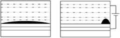
又例如,在光阀器件为电润湿光开关器件时,在未施加电压时处于非透明态,在第三电极和第四电极之间施加预定电压时处于透明态。电润湿光开关器件中,填充有透明的电解质溶液和不溶于该电解质溶液的有色液体(如油墨),在未施加电压时,如附图6所示,油墨水平分布在第三基板的上层,呈黑态,而在施加电压时,油墨在电场和分子张力的作用下,收缩到第三基板的一侧,从而可使光路通过,呈透明态。For another example, when the light valve device is an electrowetting optical switch device, it is in a non-transparent state when no voltage is applied, and is in a transparent state when a predetermined voltage is applied between the third electrode and the fourth electrode. In the electrowetting optical switch device, it is filled with a transparent electrolyte solution and a colored liquid (such as ink) insoluble in the electrolyte solution. When no voltage is applied, as shown in Figure 6, the ink is horizontally distributed on the upper layer of the third substrate , in a black state, and when a voltage is applied, the ink shrinks to one side of the third substrate under the action of the electric field and molecular tension, so that the light path can pass through and it is in a transparent state.
又例如,在光阀器件为带有偏振片的光开关器件时,可根据实际需要做成有源光开关器件或无源光开关器件。在为有源光开关器件时,在未施加电压时处于透明态,在第三电极和第四电极之间施加电压时处于黑态,实际应用中,根据具体结构也可以是在在未施加电压时处于黑态,在施加电压时处于透明态。主要是利用正交偏振片和液晶的光偏移特性和延迟特性实现透明态和黑态。For another example, when the light valve device is an optical switch device with a polarizer, it can be made into an active optical switch device or a passive optical switch device according to actual needs. When it is an active optical switching device, it is in a transparent state when no voltage is applied, and it is in a black state when a voltage is applied between the third electrode and the fourth electrode. In practical applications, it can also be in a non-voltage applied state according to the specific structure. It is in a black state when a voltage is applied, and in a transparent state when a voltage is applied. The transparent state and the black state are mainly realized by using the light deviation and retardation characteristics of crossed polarizers and liquid crystals.
其中,如附图7所示,光阀器件21还可以是电子墨水光开关器件,在光阀器件为电子墨水光开关器件时,除了包含第三电极302和第四电极304之外,还包括设置于第二基板301和第三基板303之间的第五电极701和第六电极702,在第三电极302和第四电极304之间施加第一预定电压时光阀器件21处于黑态,在光阀器件的第五电极701和第六电极702之间施加第二预定电压时光阀器件21处于透明态。具体地,第五电极701和第六电极702与第三电极302和第四电极304之间通过绝缘层703隔离,在第三电极302和第四电极304之间施加电压时,位于透明溶液中的黑色粒子704在电场作用下在第二基板或第三基板呈水平分布,从而呈现黑态;在第五电极701和第六电极702之间施加电压时,位于透明溶液中的黑色粒子704在电场作用下集中于左右两侧,且垂直于第二基板301和第三基板303分布,从而使光路通过,呈现透明态。Wherein, as shown in FIG. 7 , the
以上对光阀器件所进行的仅是列举说明,实际应用中,光阀器件并不仅限于以上几种,只要光阀器件在电场作用下,能够实现透明态和非透明态两种状态,均可用于实现OLED显示的装置的透明显示效果和普通非透明显示效果,本实施例均包括在内。The light valve devices mentioned above are just examples. In practical applications, light valve devices are not limited to the above types. As long as the light valve device can realize two states of transparent state and non-transparent state under the action of an electric field, it can be used. Both the transparent display effect and the common non-transparent display effect of the device for realizing OLED display are included in this embodiment.
本发明实施例的一种具体实现中,透明OLED显示面板的第一电极202和第二电极206均为透明材料,可以实现显示装置的双向透明显示,即从透明OLED显示面板前方可以看到正常显示的数据内容,且可以观察到位于显示装置后方的陈列物品或外界活动,同时,从显示装置的后方也可以看到显示内容。该实现方式可以通过光阀器件状态的转换,实现显示装置普通非透明显示效果和双向透明显示效果的切换。In a specific implementation of the embodiment of the present invention, the
在另一中具体实现中,透明OLED显示面板的第一电极202可以采用非透明材料,且仅覆盖像素的一部分,而第二电极采用透明材料。例如,在透明OLED的第一电极(即靠近显示装置后方的电极,又称背面电极)采用不透明的金属材料,并使该第一电极的金属线的线宽变细,使得第一电极的金属线仅覆盖像素的一部分,在光阀器件处于透明态时,利用未被金属线覆盖的像素部分可以使得用户从透明OLED显示面板的前方看到显示面板正常显示的数据内容时,同时看到显示装置后方放置的物品,而由于第一电极采用不透明的金属材料,OLED发光层发出的光线多从正面射出,此时,在光阀器件处于透明态时,从显示装置的后方很难看到显示面板显示的数据内容,从而实现单侧透明显示效果,相较于双向透明显示可以提高安全性,进一步提升用户体验。该实现方式可以通过光阀器件状态的转换,实现显示装置的普通非透明显示效果和单向透明显示效果的切换。In another specific implementation, the
在一个较佳地实现方式中,在光阀器件的第三电极和第四电极之间连接的电源电路中串接一受控开关,该受控开关根据接收的触发信号控制该受控开关的开关状态,由受控开关的开关状态控制光阀器件在非透明态和透明态之间切换。实际应用中,该受控开关可以有多种实现方式,例如,受控开关可以是光控开关(如红外控制),也可以是触控开关(如外界触摸按钮)、键控开关(如外设按键或按钮等)等。In a preferred implementation, a controlled switch is connected in series in the power supply circuit connected between the third electrode and the fourth electrode of the light valve device, and the controlled switch controls the controlled switch according to the received trigger signal. Switching state, the switching state of the controlled switch controls the light valve device to switch between the non-transparent state and the transparent state. In practical applications, the controlled switch can be realized in many ways. For example, the controlled switch can be a light-controlled switch (such as infrared control), a touch switch (such as an external touch button), a key switch (such as an external set keys or buttons, etc.), etc.
在一个较佳的实现方式中,可以控制光阀器件进行局部透明显示,具体地:在光阀器件的第二基板设置第三电极时,将第三电极设置为包含一个以上的电极区,或者,在第三基板设置第四电极时,将第四电极设置为包含一个以上的电极区,通过控制第三电极或第四电极中不同电极区上施加的电压控制相应的区域进行透明显示。该实现方案中,还需要设置光阀器件的驱动电路,该驱动电路在触发信号的控制下,控制光阀器件的相应区域在非透明态和透明态之间切换,实现局部透明显示。In a preferred implementation manner, the light valve device can be controlled to perform partial transparent display, specifically: when the third electrode is provided on the second substrate of the light valve device, the third electrode is set to include more than one electrode area, or , when the fourth electrode is provided on the third substrate, the fourth electrode is set to include more than one electrode area, and the corresponding area is controlled to perform transparent display by controlling the voltage applied to different electrode areas in the third electrode or the fourth electrode. In this implementation scheme, a drive circuit for the light valve device also needs to be provided. Under the control of the trigger signal, the drive circuit controls the corresponding area of the light valve device to switch between a non-transparent state and a transparent state to realize partial transparent display.
例如,如附图8所示,第三电极为图8中a所示,仅包含一个电极区,而第四电极在设置为图8中b所示的两个电极区时,通过将第三电极设置公共电极,将第四电极中的一个电极区设置公共电极区,而另一个电极区域设置为透明显示区域对应的电极区,则可以实现显示装置的上半部分或下半部分的透明显示,同理,第四电极采用附图8中c所示可以实现左半部分或右半部分的透明显示,而第四电极采用附图8中d所示可以实现四个区域中某一个或一个以上区域的透明显示。基于同样的原理,也可以同时将第三电极划分为两个或两个以上的电极区,同时控制第三电极和第四电极相应的电极区上施加的电压可以实现局部区域透明显示。For example, as shown in accompanying drawing 8, the third electrode is shown in a in Fig. 8, and only includes one electrode area, and when the fourth electrode is set as two electrode areas shown in b in Fig. 8, by combining the third The electrodes are provided with a common electrode, and one electrode area in the fourth electrode is set as a common electrode area, and the other electrode area is set as an electrode area corresponding to the transparent display area, so that the transparent display of the upper half or the lower half of the display device can be realized , similarly, the transparent display of the left half or the right half can be realized by using the fourth electrode as shown in c in Figure 8, and the fourth electrode can realize one or one of the four regions by using Transparent display of the above area. Based on the same principle, the third electrode can also be divided into two or more electrode areas at the same time, and the voltage applied to the corresponding electrode areas of the third electrode and the fourth electrode can be controlled simultaneously to realize transparent display in a local area.
在一个较佳的实施方式中,可以实现对光阀器件精确到像素级别的局部区域透明显示,该方案中需要将在第二基板和第三基板上设置像素电极(即光阀器件的第二基板和第三基板均为阵列基板),通过驱动电路驱动像素电极,从而实现任意大小区域的透明显示效果,实现任意大小区域的透明显示和非透明显示的切换。In a preferred embodiment, the transparent display of the local area of the light valve device accurate to the pixel level can be realized. In this solution, pixel electrodes (that is, the second substrate of the light valve device) need to be arranged on the second substrate and the third substrate. The substrate and the third substrate are both array substrates), and the pixel electrodes are driven by a driving circuit, so as to realize the transparent display effect of an area of any size, and realize the switching between transparent display and non-transparent display of an area of any size.
本发明实施例还提供了多种情况下有机发光二极管显示装置的制作方法,具体如下:Embodiments of the present invention also provide methods for manufacturing organic light-emitting diode display devices in various situations, specifically as follows:
第一种情况,如附图9所示,在透明OLED显示面板的第一基板和光阀器件的第二基板均为硬性基板时,OLED显示装置的具体制作方法如下:In the first case, as shown in Figure 9, when both the first substrate of the transparent OLED display panel and the second substrate of the light valve device are rigid substrates, the specific manufacturing method of the OLED display device is as follows:
步骤901:在透明OLED显示面板的第一基板上形成光阀器件的第三电极。Step 901: forming a third electrode of a light valve device on a first substrate of a transparent OLED display panel.
实际应用中,可以采用溅射(sputter)工艺在第一基板上形成光阀器件的第三电极。根据实际需要,还可以结合相应的构图工艺形成第三电极(例如,ITO电极)。In practical applications, a sputtering (sputter) process may be used to form the third electrode of the light valve device on the first substrate. According to actual needs, a third electrode (for example, an ITO electrode) may also be formed in combination with a corresponding patterning process.
本实施例中,直接在OLED显示面板的第一基板上形成光阀区别的第三电极,即光阀器件与OLED共用第一基板。In this embodiment, the third electrode that is different from the light valve is directly formed on the first substrate of the OLED display panel, that is, the light valve device and the OLED share the first substrate.
较佳地,在第一基板上形成光阀器件的第三电极之前,将第一基板减薄。Preferably, before forming the third electrode of the light valve device on the first substrate, the first substrate is thinned.
步骤902:在第三基板上形成光阀器件的第四电极。Step 902: forming a fourth electrode of a light valve device on a third substrate.
本实施例中,可以采用sputter工艺在第三基板上形成第四电极(例如,ITO电极)。In this embodiment, a sputter process may be used to form a fourth electrode (for example, an ITO electrode) on the third substrate.
步骤903:在第三电极和第四电极之间填充显示介质,形成光阀器件,该光阀器件在电场的作用下具有两种状态,该至少两种状态包括透明态和非透明态。Step 903: filling display media between the third electrode and the fourth electrode to form a light valve device, the light valve device has two states under the action of an electric field, the at least two states include a transparent state and a non-transparent state.
在一个具体的制作方法中,进行封框胶印制后,将第三基板和第一基板进行真空对合组装并切割后,通过灌注工艺将显示介质填充至第三电极和第四电极之间,并对第三基板进行紫外固化,实现光阀器件和OLED显示面板的集成。In a specific manufacturing method, after printing the sealant, the third substrate and the first substrate are vacuum assembled and cut, and the display medium is filled between the third electrode and the fourth electrode through a pouring process, And UV curing is performed on the third substrate to realize the integration of the light valve device and the OLED display panel.
在另一个具体的制作方法中,进行封框胶印制后,通过滴注工艺,填充显示介质后将第三基板与第一基板进行真空对合组装,并对第三基板进行紫外固化,实现光阀器件和OLED显示面板的集成,最后再进行切割。In another specific manufacturing method, after the frame sealant is printed, the display medium is filled with the dripping process, the third substrate and the first substrate are vacuum-coupled and assembled, and the third substrate is cured by ultraviolet light to realize optical Integration of valve devices and OLED display panels, and finally cutting.
其中,第三电极和第四电极之间填充的显示介质,至少包括聚合物分散液晶、胆甾液晶、电子墨水、油墨和电解质的混合溶液中的任意一种。此处仅为举例,实际应用中,也可以是其他能够使得光阀器件具有透明态和非透明态两种状态的溶液。例如,附图10所示为通过上述制作方法形成的OLED显示装置的剖面结构示意图,其中,1001为透明的阴极,1002为电子传输层,1003为有机发光层,1004为空穴传输层,1005为透明的阳极,1006为玻璃基板,1007为ITO电极,1008为显示介质,1009为ITO电极,1010为玻璃基板。Wherein, the display medium filled between the third electrode and the fourth electrode at least includes any one of polymer dispersed liquid crystal, cholesteric liquid crystal, electronic ink, and mixed solution of ink and electrolyte. This is only an example, and in practical applications, other solutions that can make the light valve device have two states, transparent state and non-transparent state, may also be used. For example, Figure 10 is a schematic cross-sectional structure diagram of an OLED display device formed by the above manufacturing method, wherein 1001 is a transparent cathode, 1002 is an electron transport layer, 1003 is an organic light-emitting layer, 1004 is a hole transport layer, 1005 1006 is a glass substrate, 1007 is an ITO electrode, 1008 is a display medium, 1009 is an ITO electrode, and 1010 is a glass substrate.
第二种情况,在透明OLED显示面板的第一基板为硬性基板时,通过贴服设备将采用柔性基板的光阀器件贴服于第一基板上;或者,在第一基板为柔性基板时,通过滚对滚(roll to roll)设备将采用柔性基板的光阀器件贴服于第一基板上,光阀器件在电场的作用下至少具有两种状态,该至少两种状态包括透明态和非透明态。In the second case, when the first substrate of the transparent OLED display panel is a rigid substrate, the light valve device using a flexible substrate is pasted on the first substrate by an attachment device; or, when the first substrate is a flexible substrate, The light valve device using the flexible substrate is attached to the first substrate by rolling to roll equipment, and the light valve device has at least two states under the action of the electric field, and the at least two states include transparent state and non-transparent state. transparent state.
较佳地,通过贴服设备将采用柔性基板的光阀器件贴服于第一基板之前,或者,通过滚对滚设备将采用柔性基板的光阀器件贴服于第一基板之前,在光阀器件和第一基板之间填充高透过率材料,该高透过率材料在紫外固化或热固化后具有粘结性。例如,该高透过率材料为聚甲基丙烯酸甲酯(PMMA)。Preferably, before the light valve device adopting the flexible substrate is adhered to the first substrate by a sticking device, or before the light valve device adopting a flexible substrate is adhered to the first substrate by roll-to-roll equipment, before the light valve A high-transmittance material is filled between the device and the first substrate, and the high-transmittance material has adhesiveness after ultraviolet curing or thermal curing. For example, the high transmittance material is polymethyl methacrylate (PMMA).
同时,本发明实施例还提供了一种显示系统,该显示系统包括上述的OLED显示装置。Meanwhile, an embodiment of the present invention also provides a display system, which includes the above-mentioned OLED display device.
较佳地,显示系统还包括位于光阀器件之后的背板保护装置,该背板保护装置采用高透过率的材料制成。Preferably, the display system further includes a back plate protection device behind the light valve device, and the back plate protection device is made of high transmittance material.
具体地,如附图11所示,显示系统除了包含透明OLED显示面板1101、位于透明OLED显示面板之后的光阀器件1102和位于光阀器件1102之后的背板保护装置1103外,还包括支柱1104,该支柱1104中可以设置电路板或电路信号传输通道,并且,该支柱1104还连接有底座1105。实际应用中,底座1105中还设置有驱动板、控制装置或外端按钮等。Specifically, as shown in FIG. 11 , the display system includes a transparent
实际应用中,在OLED显示面板1101的显示面上还可以设置触控面板。该触控面板可以有多种实现方式,例如可以是电容式、电阻式或其他方式的触摸屏。In practical applications, a touch panel may also be provided on the display surface of the
实际应用中,显示系统可以是计算机、移动终端、电视等。例如,可以是台式电脑、便携式电脑、手机、平板电脑、掌上终端设备等。附图12所示为应用上述显示装置的便携式电脑的结构示意图,其中,1201为OLED显示面板、1202为光阀器件、1203为高透过率的背板保护装置,1204为驱动板、控制器及外端键盘、按钮等设备。In practical applications, the display system may be a computer, a mobile terminal, a television, and the like. For example, it may be a desktop computer, a portable computer, a mobile phone, a tablet computer, a handheld terminal device, and the like. Accompanying drawing 12 is a schematic structural diagram of a portable computer using the above-mentioned display device, wherein 1201 is an OLED display panel, 1202 is a light valve device, 1203 is a backplane protection device with high transmittance, and 1204 is a driving board and a controller And external keyboard, buttons and other equipment.
基于上述技术方案,本发明实施例中,通过在透明OLED显示面板非显示面上设置光阀器件,该光阀器件在电场的作用下至少具有透明态和非透明态两种状态,从而可以实现在光阀器件处于透明态时,使显示装置处于透明态,能够在正常进行数据显示的同时,观察到位于显示装置后面的物体,而在光阀器件处于非透明态时,使显示装置实现普通的非透明显示效果,从而能够通过光阀器件的状态转换,实现普通非透明显示和透明显示的切换,使显示装置兼容普通非透明显示和透明显示。并且,在OLED非显示面上设置光阀器件可以结合OLED本身的重量轻、厚度薄的特点,实现可兼容普通非透明显示和透视显示效果的显示装置的轻型化和薄型化,提高用户体验。并且,本发明实施例提供的OLED显示装置具有广泛的应用,可用于各领域的显示设备,例如可以用于台式计算机、笔记本电脑、电视机、监控设备、手机等各种移动终端设备等,还可以用于医用监视器,以及各种展览场合中的显示设备,并可用于具有与其他附加功能相兼容的显示设备。Based on the above technical solution, in the embodiment of the present invention, by disposing a light valve device on the non-display surface of the transparent OLED display panel, the light valve device has at least two states of a transparent state and a non-transparent state under the action of an electric field, thereby realizing When the light valve device is in a transparent state, the display device is in a transparent state, and objects located behind the display device can be observed while performing data display normally, and when the light valve device is in a non-transparent state, the display device can realize normal The non-transparent display effect, so that the switching between ordinary non-transparent display and transparent display can be realized through the state transition of the light valve device, so that the display device is compatible with ordinary non-transparent display and transparent display. Moreover, disposing a light valve device on the non-display surface of the OLED can combine the characteristics of light weight and thin thickness of the OLED itself to realize a light and thin display device compatible with ordinary non-transparent display and see-through display effects, and improve user experience. Moreover, the OLED display device provided by the embodiments of the present invention has a wide range of applications and can be used in display devices in various fields, for example, it can be used in various mobile terminal devices such as desktop computers, notebook computers, televisions, monitoring equipment, and mobile phones. It can be used in medical monitors and display devices in various exhibition occasions, and can be used in display devices compatible with other additional functions.
显然,本领域的技术人员可以对本发明进行各种改动和变型而不脱离本发明的精神和范围。这样,倘若本发明的这些修改和变型属于本发明权利要求及其等同技术的范围之内,则本发明也意图包含这些改动和变型在内。Obviously, those skilled in the art can make various changes and modifications to the present invention without departing from the spirit and scope of the present invention. Thus, if these modifications and variations of the present invention fall within the scope of the claims of the present invention and their equivalent technologies, the present invention also intends to include these modifications and variations.
Claims (18)
Priority Applications (3)
| Application Number | Priority Date | Filing Date | Title |
|---|---|---|---|
| CN201210013274.5ACN102646696B (en) | 2012-01-16 | 2012-01-16 | Organic light-emitting diode display device, manufacturing method thereof and display system |
| PCT/CN2012/083155WO2013107194A1 (en) | 2012-01-16 | 2012-10-18 | Organic light-emitting diode display device, manufacturing method and display system |
| US13/994,737US9395576B2 (en) | 2012-01-16 | 2012-10-18 | Organic light emitting diode display device, manufacturing method for the same and display system |
Applications Claiming Priority (1)
| Application Number | Priority Date | Filing Date | Title |
|---|---|---|---|
| CN201210013274.5ACN102646696B (en) | 2012-01-16 | 2012-01-16 | Organic light-emitting diode display device, manufacturing method thereof and display system |
Publications (2)
| Publication Number | Publication Date |
|---|---|
| CN102646696Atrue CN102646696A (en) | 2012-08-22 |
| CN102646696B CN102646696B (en) | 2014-10-22 |
Family
ID=46659410
Family Applications (1)
| Application Number | Title | Priority Date | Filing Date |
|---|---|---|---|
| CN201210013274.5AActiveCN102646696B (en) | 2012-01-16 | 2012-01-16 | Organic light-emitting diode display device, manufacturing method thereof and display system |
Country Status (3)
| Country | Link |
|---|---|
| US (1) | US9395576B2 (en) |
| CN (1) | CN102646696B (en) |
| WO (1) | WO2013107194A1 (en) |
Cited By (23)
| Publication number | Priority date | Publication date | Assignee | Title |
|---|---|---|---|---|
| WO2013107194A1 (en)* | 2012-01-16 | 2013-07-25 | 京东方科技集团股份有限公司 | Organic light-emitting diode display device, manufacturing method and display system |
| WO2014029805A1 (en)* | 2012-08-24 | 2014-02-27 | Osram Opto Semiconductors Gmbh | Organic light-emitting diode and method for operating an organic light-emitting diode |
| WO2014173148A1 (en)* | 2013-04-27 | 2014-10-30 | 京东方科技集团股份有限公司 | Baffle board and transparent display apparatus |
| DE102013106992A1 (en)* | 2013-07-03 | 2015-01-08 | Osram Oled Gmbh | Optoelectronic component, method for producing an optoelectronic component |
| WO2015021718A1 (en)* | 2013-08-14 | 2015-02-19 | 京东方科技集团股份有限公司 | Display apparatus and display control method |
| CN105206644A (en)* | 2015-08-28 | 2015-12-30 | 京东方科技集团股份有限公司 | Transparent display assembly and display device |
| CN106406595A (en)* | 2015-07-31 | 2017-02-15 | 明兴光电股份有限公司 | Touch control device |
| CN106684261A (en)* | 2017-01-22 | 2017-05-17 | 昆山工研院新型平板显示技术中心有限公司 | Transparency adjustment unit and display device |
| CN106842726A (en)* | 2017-03-23 | 2017-06-13 | 奇酷互联网络科技(深圳)有限公司 | Display device |
| CN107195668A (en)* | 2017-07-17 | 2017-09-22 | 深圳市华星光电半导体显示技术有限公司 | A kind of array base palte, display panel and display device |
| US9846343B2 (en) | 2013-08-14 | 2017-12-19 | Boe Technology Group Co., Ltd. | Display device and display control method |
| CN108027549A (en)* | 2015-07-03 | 2018-05-11 | 贤纳科技有限公司 | Display system |
| CN108169974A (en)* | 2018-01-22 | 2018-06-15 | 京东方科技集团股份有限公司 | A kind of transparent display and its display methods |
| CN108254963A (en)* | 2018-03-20 | 2018-07-06 | 京东方科技集团股份有限公司 | A kind of display panel, display module, display device and its driving method |
| CN108962027A (en)* | 2018-07-08 | 2018-12-07 | 王子韩 | A kind of double screen outdoor advertisement device shown based on transparent flexible |
| CN109104510A (en)* | 2018-08-31 | 2018-12-28 | 武汉华星光电技术有限公司 | Display device and display methods |
| CN109713163A (en)* | 2018-12-27 | 2019-05-03 | 厦门天马微电子有限公司 | Organic light emitting display panel and preparation method thereof, display device |
| WO2019206180A1 (en)* | 2018-04-26 | 2019-10-31 | 京东方科技集团股份有限公司 | Display panel and driving method therefor, and display device |
| CN110596945A (en)* | 2019-09-20 | 2019-12-20 | 厦门天马微电子有限公司 | Display panel and display device |
| TWI680576B (en)* | 2019-03-20 | 2019-12-21 | 大陸商業成科技(成都)有限公司 | Organic light emitting diode display panel and method for making thereof |
| CN110767693A (en)* | 2018-12-14 | 2020-02-07 | 昆山国显光电有限公司 | Array substrate, display screen and display terminal |
| CN113031318A (en)* | 2021-04-22 | 2021-06-25 | 福州京东方光电科技有限公司 | Light valve element and liquid crystal display device |
| CN115047662A (en)* | 2015-08-31 | 2022-09-13 | 乐金显示有限公司 | Transparent display device and method of manufacturing the same |
Families Citing this family (4)
| Publication number | Priority date | Publication date | Assignee | Title |
|---|---|---|---|---|
| CN105549319B (en)* | 2016-02-25 | 2019-10-25 | 京东方科技集团股份有限公司 | Mask and mask exposure method, mask system and pattern control device |
| US10411041B2 (en) | 2017-07-17 | 2019-09-10 | Shenzhen China Star Optoelectronics Semiconductor Display Technology Co., Ltd | Array substrate, display panel, and display device |
| KR102721329B1 (en)* | 2019-03-27 | 2024-10-23 | 주식회사 엘지화학 | Transparent light emitting device display |
| CN113964152B (en)* | 2020-07-21 | 2025-08-26 | Oppo广东移动通信有限公司 | Display panel, electronic device, shooting control method and storage medium |
Citations (8)
| Publication number | Priority date | Publication date | Assignee | Title |
|---|---|---|---|---|
| CN1875391A (en)* | 2003-11-06 | 2006-12-06 | 皇家飞利浦电子股份有限公司 | Switchable transparent display |
| US20070057932A1 (en)* | 2005-09-13 | 2007-03-15 | Shin Hyun S | Flat panel display and organic light emitting display |
| CN201355416Y (en)* | 2008-12-19 | 2009-12-02 | 康佳集团股份有限公司 | Touch screen with lighting function |
| EP2169966A2 (en)* | 2008-09-30 | 2010-03-31 | Samsung Electronics Co., Ltd. | 2D/3D Switchable autostereoscopic display apparatus and method |
| CN101923243A (en)* | 2009-04-27 | 2010-12-22 | 宝创有限公司 | Polymeric dispersed liquid crystal light shutter device |
| CN201796892U (en)* | 2010-09-17 | 2011-04-13 | 四川虹视显示技术有限公司 | OLED device with both sides emitting light |
| CN102257651A (en)* | 2008-12-19 | 2011-11-23 | 皇家飞利浦电子股份有限公司 | Transparent organic light emitting diode |
| CN202487668U (en)* | 2012-01-16 | 2012-10-10 | 京东方科技集团股份有限公司 | An organic light emitting diode display device and display system |
Family Cites Families (2)
| Publication number | Priority date | Publication date | Assignee | Title |
|---|---|---|---|---|
| US6856086B2 (en)* | 2001-06-25 | 2005-02-15 | Avery Dennison Corporation | Hybrid display device |
| CN102646696B (en)* | 2012-01-16 | 2014-10-22 | 京东方科技集团股份有限公司 | Organic light-emitting diode display device, manufacturing method thereof and display system |
- 2012
- 2012-01-16CNCN201210013274.5Apatent/CN102646696B/enactiveActive
- 2012-10-18WOPCT/CN2012/083155patent/WO2013107194A1/enactiveApplication Filing
- 2012-10-18USUS13/994,737patent/US9395576B2/enactiveActive
Patent Citations (8)
| Publication number | Priority date | Publication date | Assignee | Title |
|---|---|---|---|---|
| CN1875391A (en)* | 2003-11-06 | 2006-12-06 | 皇家飞利浦电子股份有限公司 | Switchable transparent display |
| US20070057932A1 (en)* | 2005-09-13 | 2007-03-15 | Shin Hyun S | Flat panel display and organic light emitting display |
| EP2169966A2 (en)* | 2008-09-30 | 2010-03-31 | Samsung Electronics Co., Ltd. | 2D/3D Switchable autostereoscopic display apparatus and method |
| CN201355416Y (en)* | 2008-12-19 | 2009-12-02 | 康佳集团股份有限公司 | Touch screen with lighting function |
| CN102257651A (en)* | 2008-12-19 | 2011-11-23 | 皇家飞利浦电子股份有限公司 | Transparent organic light emitting diode |
| CN101923243A (en)* | 2009-04-27 | 2010-12-22 | 宝创有限公司 | Polymeric dispersed liquid crystal light shutter device |
| CN201796892U (en)* | 2010-09-17 | 2011-04-13 | 四川虹视显示技术有限公司 | OLED device with both sides emitting light |
| CN202487668U (en)* | 2012-01-16 | 2012-10-10 | 京东方科技集团股份有限公司 | An organic light emitting diode display device and display system |
Cited By (37)
| Publication number | Priority date | Publication date | Assignee | Title |
|---|---|---|---|---|
| WO2013107194A1 (en)* | 2012-01-16 | 2013-07-25 | 京东方科技集团股份有限公司 | Organic light-emitting diode display device, manufacturing method and display system |
| US9395576B2 (en) | 2012-01-16 | 2016-07-19 | Boe Technology Group Co., Ltd. | Organic light emitting diode display device, manufacturing method for the same and display system |
| WO2014029805A1 (en)* | 2012-08-24 | 2014-02-27 | Osram Opto Semiconductors Gmbh | Organic light-emitting diode and method for operating an organic light-emitting diode |
| WO2014173148A1 (en)* | 2013-04-27 | 2014-10-30 | 京东方科技集团股份有限公司 | Baffle board and transparent display apparatus |
| CN103217827B (en)* | 2013-04-27 | 2015-07-08 | 京东方科技集团股份有限公司 | Transparent display device |
| DE102013106992A1 (en)* | 2013-07-03 | 2015-01-08 | Osram Oled Gmbh | Optoelectronic component, method for producing an optoelectronic component |
| US9846343B2 (en) | 2013-08-14 | 2017-12-19 | Boe Technology Group Co., Ltd. | Display device and display control method |
| WO2015021718A1 (en)* | 2013-08-14 | 2015-02-19 | 京东方科技集团股份有限公司 | Display apparatus and display control method |
| CN108027549A (en)* | 2015-07-03 | 2018-05-11 | 贤纳科技有限公司 | Display system |
| CN106406595A (en)* | 2015-07-31 | 2017-02-15 | 明兴光电股份有限公司 | Touch control device |
| CN105206644A (en)* | 2015-08-28 | 2015-12-30 | 京东方科技集团股份有限公司 | Transparent display assembly and display device |
| WO2017036064A1 (en)* | 2015-08-28 | 2017-03-09 | 京东方科技集团股份有限公司 | Transparent display assembly and display device |
| CN115047662A (en)* | 2015-08-31 | 2022-09-13 | 乐金显示有限公司 | Transparent display device and method of manufacturing the same |
| CN115047662B (en)* | 2015-08-31 | 2025-02-18 | 乐金显示有限公司 | Transparent display device and manufacturing method thereof |
| CN106684261B (en)* | 2017-01-22 | 2019-01-18 | 昆山工研院新型平板显示技术中心有限公司 | Transparency adjusts unit and display device |
| CN106684261A (en)* | 2017-01-22 | 2017-05-17 | 昆山工研院新型平板显示技术中心有限公司 | Transparency adjustment unit and display device |
| CN106842726A (en)* | 2017-03-23 | 2017-06-13 | 奇酷互联网络科技(深圳)有限公司 | Display device |
| CN107195668B (en)* | 2017-07-17 | 2018-06-15 | 深圳市华星光电半导体显示技术有限公司 | A kind of array substrate, display panel and display device |
| CN107195668A (en)* | 2017-07-17 | 2017-09-22 | 深圳市华星光电半导体显示技术有限公司 | A kind of array base palte, display panel and display device |
| CN108169974A (en)* | 2018-01-22 | 2018-06-15 | 京东方科技集团股份有限公司 | A kind of transparent display and its display methods |
| CN108169974B (en)* | 2018-01-22 | 2022-04-12 | 京东方科技集团股份有限公司 | Transparent display device and display method thereof |
| CN108254963A (en)* | 2018-03-20 | 2018-07-06 | 京东方科技集团股份有限公司 | A kind of display panel, display module, display device and its driving method |
| WO2019179217A1 (en)* | 2018-03-20 | 2019-09-26 | 京东方科技集团股份有限公司 | Display panel, display component, display apparatus and drive method therefor |
| US11270628B2 (en) | 2018-03-20 | 2022-03-08 | Beijing Boe Display Technology Co., Ltd. | Display panel, display assembly, display apparatus and drive method therefor |
| US10976604B2 (en) | 2018-04-26 | 2021-04-13 | Boe Technology Group Co., Ltd. | Display panel, driving method thereof and display device |
| WO2019206180A1 (en)* | 2018-04-26 | 2019-10-31 | 京东方科技集团股份有限公司 | Display panel and driving method therefor, and display device |
| CN108962027A (en)* | 2018-07-08 | 2018-12-07 | 王子韩 | A kind of double screen outdoor advertisement device shown based on transparent flexible |
| WO2020042272A1 (en)* | 2018-08-31 | 2020-03-05 | 武汉华星光电技术有限公司 | Display device and display method |
| US11069324B1 (en) | 2018-08-31 | 2021-07-20 | Wuhan China Star Optoelectronics Technology Co., Ltd | Display device and display method background of the disclosure |
| CN109104510A (en)* | 2018-08-31 | 2018-12-28 | 武汉华星光电技术有限公司 | Display device and display methods |
| CN110767693A (en)* | 2018-12-14 | 2020-02-07 | 昆山国显光电有限公司 | Array substrate, display screen and display terminal |
| CN110767693B (en)* | 2018-12-14 | 2022-07-19 | 昆山国显光电有限公司 | Array substrate, display screen and display terminal |
| CN109713163B (en)* | 2018-12-27 | 2021-07-16 | 厦门天马微电子有限公司 | Organic light-emitting display panel, manufacturing method thereof and display device |
| CN109713163A (en)* | 2018-12-27 | 2019-05-03 | 厦门天马微电子有限公司 | Organic light emitting display panel and preparation method thereof, display device |
| TWI680576B (en)* | 2019-03-20 | 2019-12-21 | 大陸商業成科技(成都)有限公司 | Organic light emitting diode display panel and method for making thereof |
| CN110596945A (en)* | 2019-09-20 | 2019-12-20 | 厦门天马微电子有限公司 | Display panel and display device |
| CN113031318A (en)* | 2021-04-22 | 2021-06-25 | 福州京东方光电科技有限公司 | Light valve element and liquid crystal display device |
Also Published As
| Publication number | Publication date |
|---|---|
| US9395576B2 (en) | 2016-07-19 |
| CN102646696B (en) | 2014-10-22 |
| WO2013107194A1 (en) | 2013-07-25 |
| US20140055718A1 (en) | 2014-02-27 |
Similar Documents
| Publication | Publication Date | Title |
|---|---|---|
| CN102646696B (en) | Organic light-emitting diode display device, manufacturing method thereof and display system | |
| US9772538B2 (en) | Transparent display device | |
| Heo et al. | Fast-switching initially-transparent liquid crystal light shutter with crossed patterned electrodes | |
| US9804467B2 (en) | Light controlling apparatus and method of fabricating the same | |
| JP5640178B1 (en) | Liquid crystal display | |
| US10036915B2 (en) | Method for manufacturing PDLC display device and PDLC display device | |
| US9857623B2 (en) | Reflective flexible liquid crystal display | |
| CN202487668U (en) | An organic light emitting diode display device and display system | |
| CN201069505Y (en) | Dual-face display | |
| CN106154604A (en) | Peep-proof film and peep-proof system, display base plate and display device | |
| CN107632727B (en) | Touch display screen and manufacturing method thereof, display device and driving method | |
| WO2021082804A1 (en) | Display device and electronic apparatus | |
| EP1987709A1 (en) | A display module and method for fixing | |
| CN102955284A (en) | Display and electronic unit | |
| CN108169953A (en) | A kind of peep-proof shows equipment and its switching method | |
| WO2016103629A1 (en) | Optical device | |
| CN108681133A (en) | Display panel and display methods and vehicle-mounted head-up display system | |
| CN105549282A (en) | Transparent displayer | |
| US10191325B2 (en) | Liquid crystal display device and liquid crystal display panel thereof | |
| EP3153918B1 (en) | Transflective type liquid crystal display device and driving method thereof | |
| CN102819154A (en) | Liquid crystal panel and display device | |
| CN104375703B (en) | Low reflection touching display screen | |
| KR20140024642A (en) | Transparent display with excellent visibility using pdlc film | |
| CN104050930A (en) | Display device and display control method | |
| CN211426978U (en) | Viewing angle control device and display device |
Legal Events
| Date | Code | Title | Description |
|---|---|---|---|
| C06 | Publication | ||
| PB01 | Publication | ||
| C10 | Entry into substantive examination | ||
| SE01 | Entry into force of request for substantive examination | ||
| C14 | Grant of patent or utility model | ||
| GR01 | Patent grant |