CN102645808A - Method for manufacturing array substrate, array substrate and display device - Google Patents
Method for manufacturing array substrate, array substrate and display deviceDownload PDFInfo
- Publication number
- CN102645808A CN102645808ACN2012101190080ACN201210119008ACN102645808ACN 102645808 ACN102645808 ACN 102645808ACN 2012101190080 ACN2012101190080 ACN 2012101190080ACN 201210119008 ACN201210119008 ACN 201210119008ACN 102645808 ACN102645808 ACN 102645808A
- Authority
- CN
- China
- Prior art keywords
- electrode
- insulating film
- data line
- layer
- substrate
- Prior art date
- Legal status (The legal status is an assumption and is not a legal conclusion. Google has not performed a legal analysis and makes no representation as to the accuracy of the status listed.)
- Pending
Links
Images


Classifications
- G—PHYSICS
- G02—OPTICS
- G02F—OPTICAL DEVICES OR ARRANGEMENTS FOR THE CONTROL OF LIGHT BY MODIFICATION OF THE OPTICAL PROPERTIES OF THE MEDIA OF THE ELEMENTS INVOLVED THEREIN; NON-LINEAR OPTICS; FREQUENCY-CHANGING OF LIGHT; OPTICAL LOGIC ELEMENTS; OPTICAL ANALOGUE/DIGITAL CONVERTERS
- G02F1/00—Devices or arrangements for the control of the intensity, colour, phase, polarisation or direction of light arriving from an independent light source, e.g. switching, gating or modulating; Non-linear optics
- G02F1/01—Devices or arrangements for the control of the intensity, colour, phase, polarisation or direction of light arriving from an independent light source, e.g. switching, gating or modulating; Non-linear optics for the control of the intensity, phase, polarisation or colour
- G02F1/13—Devices or arrangements for the control of the intensity, colour, phase, polarisation or direction of light arriving from an independent light source, e.g. switching, gating or modulating; Non-linear optics for the control of the intensity, phase, polarisation or colour based on liquid crystals, e.g. single liquid crystal display cells
- G02F1/133—Constructional arrangements; Operation of liquid crystal cells; Circuit arrangements
- G02F1/1333—Constructional arrangements; Manufacturing methods
- G02F1/1343—Electrodes
- G02F1/134309—Electrodes characterised by their geometrical arrangement
- G02F1/134363—Electrodes characterised by their geometrical arrangement for applying an electric field parallel to the substrate, i.e. in-plane switching [IPS]
- G—PHYSICS
- G02—OPTICS
- G02F—OPTICAL DEVICES OR ARRANGEMENTS FOR THE CONTROL OF LIGHT BY MODIFICATION OF THE OPTICAL PROPERTIES OF THE MEDIA OF THE ELEMENTS INVOLVED THEREIN; NON-LINEAR OPTICS; FREQUENCY-CHANGING OF LIGHT; OPTICAL LOGIC ELEMENTS; OPTICAL ANALOGUE/DIGITAL CONVERTERS
- G02F1/00—Devices or arrangements for the control of the intensity, colour, phase, polarisation or direction of light arriving from an independent light source, e.g. switching, gating or modulating; Non-linear optics
- G02F1/01—Devices or arrangements for the control of the intensity, colour, phase, polarisation or direction of light arriving from an independent light source, e.g. switching, gating or modulating; Non-linear optics for the control of the intensity, phase, polarisation or colour
- G02F1/13—Devices or arrangements for the control of the intensity, colour, phase, polarisation or direction of light arriving from an independent light source, e.g. switching, gating or modulating; Non-linear optics for the control of the intensity, phase, polarisation or colour based on liquid crystals, e.g. single liquid crystal display cells
- G02F1/133—Constructional arrangements; Operation of liquid crystal cells; Circuit arrangements
- G02F1/136—Liquid crystal cells structurally associated with a semi-conducting layer or substrate, e.g. cells forming part of an integrated circuit
- G02F1/1362—Active matrix addressed cells
Landscapes
- Physics & Mathematics (AREA)
- Nonlinear Science (AREA)
- Mathematical Physics (AREA)
- Chemical & Material Sciences (AREA)
- Crystallography & Structural Chemistry (AREA)
- General Physics & Mathematics (AREA)
- Optics & Photonics (AREA)
- Liquid Crystal (AREA)
- Geometry (AREA)
- Engineering & Computer Science (AREA)
- Microelectronics & Electronic Packaging (AREA)
- Thin Film Transistor (AREA)
Abstract
Description
Translated fromChinese技术领域technical field
本发明涉及液晶显示领域,尤其涉及一种阵列基板的制造方法、阵列基板及显示装置。The invention relates to the field of liquid crystal display, in particular to a method for manufacturing an array substrate, the array substrate and a display device.
背景技术Background technique
薄膜晶体管液晶显示器(TFT-LCD)具有体积小、功耗低、无辐射等特点,在当前的平板显示器市场中占据了主导地位。其中,高级超维场转换技术(ADvanced Super Dimension Switch,简称ADS),通过同一平面内狭缝电极边缘所产生的电场以及狭缝电极层与板状电极层间产生的电场形成多维电场,使液晶盒内狭缝电极间、电极正上方所有取向液晶分子都能够产生旋转,从而提高了液晶工作效率并增大了透光效率。高级超维场开关技术可以提高TFT-LCD产品的画面品质,具有高分辨率、高透过率、低功耗、宽视角、高开口率、低色差、无挤压水波纹(push Mura)等优点。Thin film transistor liquid crystal display (TFT-LCD) has the characteristics of small size, low power consumption, and no radiation, and occupies a dominant position in the current flat panel display market. Among them, ADvanced Super Dimension Switch (ADS for short), through the electric field generated by the edge of the slit electrode in the same plane and the electric field generated between the slit electrode layer and the plate electrode layer, forms a multi-dimensional electric field, so that the liquid crystal All oriented liquid crystal molecules between the slit electrodes in the cell and directly above the electrodes can be rotated, thereby improving the working efficiency of the liquid crystal and increasing the light transmission efficiency. Advanced ultra-dimensional field switching technology can improve the picture quality of TFT-LCD products, with high resolution, high transmittance, low power consumption, wide viewing angle, high aperture ratio, low color difference, no push Mura, etc. advantage.
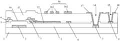
ADS模式TFT-LCD是利用公共电极和像素电极之间的边缘场效应驱动液晶,根据其电极设计及层间结构,液晶透过率及特性大有变化。图1为现有技术的ADS模式液晶显示器的阵列基板的截面图。如图1所示,在所述阵列基板中,栅电极2形成在基板1上,栅电极2上形成有栅绝缘层4,栅绝缘层4上形成有半导体层5,源电极6和漏电极7形成在半导体层5上且相互分开着,像素电极12与漏电极7电连接后形成在栅绝缘层4上,公共电极16形成在保护膜13上,栅线(图未示)和数据线8限定像素区域,栅焊盘3形成在基板1上,数据焊盘9形成在栅绝缘层4上。为了防止漏光,在数据线8上方形成一部分公共电极162。The ADS mode TFT-LCD uses the fringe field effect between the common electrode and the pixel electrode to drive the liquid crystal. According to its electrode design and interlayer structure, the transmittance and characteristics of the liquid crystal vary greatly. FIG. 1 is a cross-sectional view of an array substrate of an ADS mode liquid crystal display in the prior art. As shown in Figure 1, in the array substrate, a
在上述阵列基板中,公共电极162和数据8之间存在寄生电容(Cdp_datato Vcom),像素电极12和数据线8之间也存在寄生电容(Cdp_data to pixel)。在结构上,像素电极12和数据线8之间的距离较小时,寄生电容会比较大,这给像素电极12的充电特性带来影响,随之会影响到显示的质量,导致画面上出现污渍、残像或者闪烁现象。为此,需要增加像素电极12和数据线8之间的距离来减小寄生电容,但这却会导致像素的开口率降低。In the above array substrate, there is a parasitic capacitance (Cdp_data to Vcom) between the
另外,公共电极162和数据线8之间的寄生电容较大时,会导致数据线8上的信号发生延迟。液晶显示器的分辨率越高、面积越大时,信号延迟会越严重。在现有的改善信号延迟的方法中,主要是通过提高数据线8和公共电极162间的保护膜13的厚度来降低寄生电容,但这会造成制造时间以及制造成本的急剧增加。In addition, when the parasitic capacitance between the
发明内容Contents of the invention
本发明所要解决的技术问题是提供一种阵列基板的制造方法、阵列基板及显示装置,以降低阵列基板中数据线上的信号延迟,并防止高温下TFT中漏电流的产生。The technical problem to be solved by the present invention is to provide a method for manufacturing an array substrate, an array substrate and a display device, so as to reduce the signal delay on the data lines in the array substrate and prevent leakage current in TFTs under high temperature.
为解决上述技术问题,本发明提供技术方案如下:In order to solve the problems of the technologies described above, the present invention provides technical solutions as follows:
一种阵列基板,包括显示区域和非显示区域,所述显示区域包括栅线、数据线以及位于栅线和数据线之间的多个像素单元,所述非显示区域包括栅焊盘和数据焊盘,其中,所述像素单元包括薄膜晶体管、像素电极和公共电极,所述像素电极与所述薄膜晶体管的漏电极相连接;所述公共电极包括位于像素电极上方的第一公共电极和位于数据线上方的第二公共电极;所述公共电极所在的层与所述像素电极所在的层之间设置有保护膜;所述像素电极和所述数据线之间、以及所述薄膜晶体管与所述保护膜之间设置有无机绝缘膜和有机绝缘膜,所述无机绝缘膜形成在所述数据线和所述薄膜晶体管的源极、漏极和沟道区域的半导体层的上方,所述有机绝缘膜位于所述无机绝缘膜的上方。An array substrate includes a display area and a non-display area, the display area includes gate lines, data lines, and a plurality of pixel units between the gate lines and the data lines, and the non-display area includes gate pads and data pads disk, wherein the pixel unit includes a thin film transistor, a pixel electrode and a common electrode, and the pixel electrode is connected to the drain electrode of the thin film transistor; the common electrode includes a first common electrode located above the pixel electrode and a data the second common electrode above the line; a protective film is provided between the layer where the common electrode is located and the layer where the pixel electrode is located; between the pixel electrode and the data line, and between the thin film transistor and the An inorganic insulating film and an organic insulating film are arranged between the protective films, the inorganic insulating film is formed above the data line and the semiconductor layer of the source, drain, and channel regions of the thin film transistor, and the organic insulating film A film is located over the inorganic insulating film.
上述的阵列基板,其中,所述阵列基板的具体结构包括:The above array substrate, wherein the specific structure of the array substrate includes:
形成在基板上的栅电极和栅线;gate electrodes and gate lines formed on the substrate;
形成在栅电极和栅线上的栅绝缘层;a gate insulating layer formed on the gate electrode and the gate line;
形成在栅绝缘层上的半导体层和数据线;A semiconductor layer and a data line formed on the gate insulating layer;
形成在半导体层上的源电极和漏电极;source and drain electrodes formed on the semiconductor layer;
形成在源电极、漏电极、数据线和半导体层上的无机绝缘膜;an inorganic insulating film formed on the source electrode, the drain electrode, the data line and the semiconductor layer;
形成在无机绝缘膜上的有机绝缘膜,无机绝缘膜和有机绝缘膜上形成有第一接触孔;an organic insulating film formed on the inorganic insulating film, a first contact hole is formed on the inorganic insulating film and the organic insulating film;
形成在有机绝缘膜上的像素电极,像素电极通过第一接触孔与漏电极电连接;A pixel electrode formed on the organic insulating film, the pixel electrode is electrically connected to the drain electrode through the first contact hole;
形成在像素电极和有机绝缘膜上的保护膜;a protective film formed on the pixel electrode and the organic insulating film;
形成在保护膜上的公共电极,公共电极包括位于像素电极上方的第一公共电极和位于数据线上方的第二公共电极。A common electrode formed on the protective film, the common electrode includes a first common electrode located above the pixel electrodes and a second common electrode located above the data lines.
上述的阵列基板,其中,所述数据线下方保留有半导体层材料,或者所述数据线下方与栅绝缘层直接接触。In the above-mentioned array substrate, the material of the semiconductor layer remains under the data lines, or the underside of the data lines is in direct contact with the gate insulating layer.
上述的阵列基板,其中,还包括:The above-mentioned array substrate, which also includes:
与所述栅线位于同一层的栅焊盘;a gate pad located on the same layer as the gate line;
与所述数据线位于同一层的数据焊盘;A data pad located on the same layer as the data line;
在所述栅焊盘上方形成的第二接触孔和栅焊盘电极,所述栅焊盘电极通过所述第二接触孔与所述栅焊盘电连接;a second contact hole and a gate pad electrode formed above the gate pad, the gate pad electrode being electrically connected to the gate pad through the second contact hole;
在所述数据焊盘上方形成的第三接触孔和数据焊盘电极,所述数据焊盘电极通过所述第三接触孔与所述数据焊盘电连接。A third contact hole and a data pad electrode are formed above the data pad, and the data pad electrode is electrically connected to the data pad through the third contact hole.
上述的阵列基板,其中:所述像素电极与所述数据线在沿平行于所述基板的方向之间的距离为0~1μm。The above-mentioned array substrate, wherein: the distance between the pixel electrode and the data line along a direction parallel to the substrate is 0-1 μm.
上述的阵列基板,其中:所述无机绝缘膜的厚度为The above-mentioned array substrate, wherein: the thickness of the inorganic insulating film is
上述的阵列基板,其中:所述有机绝缘膜的材料为聚丙烯酸。In the above-mentioned array substrate, wherein: the material of the organic insulating film is polyacrylic acid.
上述的阵列基板,其中:所述有机绝缘膜的厚度为
上述的阵列基板,其中:所述保护膜采用无机绝缘材料,其厚度为
一种阵列基板的制造方法,包括:A method of manufacturing an array substrate, comprising:
在基板上形成栅电极、栅线和栅焊盘;forming gate electrodes, gate lines and gate pads on the substrate;
在形成有栅电极、栅线和栅焊盘的基板上形成栅绝缘层;forming a gate insulating layer on the substrate formed with gate electrodes, gate lines and gate pads;
在形成有栅绝缘层的基板上形成半导体层、源电极、漏电极、数据线和数据焊盘;forming a semiconductor layer, a source electrode, a drain electrode, a data line, and a data pad on the substrate on which the gate insulating layer is formed;
在形成有半导体层、源电极、漏电极、数据线和数据焊盘的基板上形成无机绝缘膜;forming an inorganic insulating film on the substrate formed with the semiconductor layer, source electrode, drain electrode, data line and data pad;
在形成有无机绝缘膜的基板上形成有机绝缘膜,对有机绝缘膜和无机绝缘膜进行构图,以形成第一接触孔,并暴露栅焊盘区域的栅绝缘层和数据焊盘;forming an organic insulating film on the substrate formed with the inorganic insulating film, patterning the organic insulating film and the inorganic insulating film to form a first contact hole, and exposing the gate insulating layer and the data pad in the gate pad region;
在形成有有机绝缘膜的基板上形成像素电极,像素电极通过第一接触孔与漏电极电连接;forming a pixel electrode on the substrate on which the organic insulating film is formed, and electrically connecting the pixel electrode to the drain electrode through the first contact hole;
在形成有像素电极的基板上形成保护膜,并对保护膜进行构图,以形成第二接触孔和第三接触孔;forming a protective film on the substrate formed with the pixel electrode, and patterning the protective film to form a second contact hole and a third contact hole;
在形成有保护膜的基板上形成公共电极、栅焊盘电极和数据焊盘电极,公共电极包括位于像素电极上方的第一公共电极和位于数据线上方的第二公共电极,栅焊盘电极通过第二接触孔与栅焊盘电连接,数据焊盘电极通过第三接触孔与数据焊盘电连接。A common electrode, a gate pad electrode, and a data pad electrode are formed on the substrate on which the protective film is formed. The common electrode includes a first common electrode above the pixel electrode and a second common electrode above the data line. The gate pad electrode passes through The second contact hole is electrically connected to the gate pad, and the data pad electrode is electrically connected to the data pad through the third contact hole.
上述的制造方法,其中,所述在形成有栅绝缘层的基板上形成半导体层、源电极、漏电极、数据线和数据焊盘,包括:The above-mentioned manufacturing method, wherein said forming the semiconductor layer, the source electrode, the drain electrode, the data line and the data pad on the substrate formed with the gate insulating layer includes:
在形成有栅绝缘层的基板上形成半导体材料层;forming a semiconductor material layer on the substrate formed with the gate insulating layer;
对半导体材料层进行构图,形成半导体层;Patterning the semiconductor material layer to form a semiconductor layer;
在形成有半导体层的基板上形成金属层;forming a metal layer on the substrate formed with the semiconductor layer;
对金属层进行构图,形成源电极、漏电极、数据线和数据焊盘,并在源电极和漏电极之间的半导体层上形成沟道。The metal layer is patterned to form source electrodes, drain electrodes, data lines and data pads, and a channel is formed on the semiconductor layer between the source electrodes and the drain electrodes.
上述的制造方法,其中,所述在形成有栅绝缘层的基板上形成半导体层、源电极、漏电极、数据线和数据焊盘,包括:The above-mentioned manufacturing method, wherein said forming the semiconductor layer, the source electrode, the drain electrode, the data line and the data pad on the substrate formed with the gate insulating layer includes:
在形成有栅绝缘层的基板上依次形成半导体材料层和金属层;sequentially forming a semiconductor material layer and a metal layer on the substrate on which the gate insulating layer is formed;
在金属层上形成光刻胶层;forming a photoresist layer on the metal layer;
采用半色调或灰色调掩模板对光刻胶层进行曝光和显影,形成光刻胶完全保留区域、光刻胶部分保留区域和光刻胶未保留区域;Exposing and developing the photoresist layer by using a half-tone or gray-tone mask to form photoresist completely reserved areas, photoresist partially reserved areas and photoresist unreserved areas;
刻蚀掉光刻胶未保留区域的金属层和半导体材料层;Etching away the metal layer and semiconductor material layer in the area where the photoresist is not retained;
通过灰化工艺去除光刻胶部分保留区域的光刻胶;Removing the photoresist in the partly reserved area of the photoresist through an ashing process;
刻蚀掉光刻胶部分保留区域的金属层及半导体材料层的一部分。Etching away a part of the metal layer and the semiconductor material layer in the partially reserved area of the photoresist.
上述的制造方法,其中,对有机绝缘膜进行构图之后,还包括:The above-mentioned manufacturing method, wherein, after patterning the organic insulating film, further includes:
对所述有机绝缘膜进行固化处理,所述固化处理的温度为230~260℃,时间为30~60分钟。The organic insulating film is cured at a temperature of 230-260° C. for 30-60 minutes.
上述的制造方法,其中:所述像素电极与所述数据线在沿平行于所述基板的方向之间的距离为0~1μm。In the above manufacturing method, wherein: the distance between the pixel electrode and the data line along a direction parallel to the substrate is 0-1 μm.
上述的制造方法,其中:所述无机绝缘膜的厚度为
上述的制造方法,其中:所述有机绝缘膜的材料为聚丙烯酸。In the above manufacturing method, wherein: the material of the organic insulating film is polyacrylic acid.
上述的制造方法,其中:所述有机绝缘膜的厚度为
上述的制造方法,其中:所述保护膜采用无极绝缘材料,其厚度为
一种显示装置,包括上述的阵列基板。A display device includes the above-mentioned array substrate.
本发明的技术方案通过将低介电常数的有机绝缘膜应用于阵列基板,来降低公共电极和数据线之间的寄生电容,从而能够降低数据线上的信号延迟,改善显示质量。相对于现有技术中通过增加保护膜的厚度来降低寄生电容,本发明的技术方案还能够减少工艺时间和降低制造成本。The technical scheme of the present invention reduces the parasitic capacitance between the common electrode and the data line by applying an organic insulating film with a low dielectric constant to the array substrate, thereby reducing signal delay on the data line and improving display quality. Compared with reducing the parasitic capacitance by increasing the thickness of the protective film in the prior art, the technical solution of the present invention can also reduce the process time and reduce the manufacturing cost.
另外,本发明的技术方案还在有机绝缘膜和半导体层之间形成无机绝缘膜作为缓冲层,所述缓冲层能够阻止有机绝缘膜中的离子异物渗透到半导体层,从而防止在高温下TFT中漏电流的产生。In addition, the technical solution of the present invention also forms an inorganic insulating film as a buffer layer between the organic insulating film and the semiconductor layer, and the buffer layer can prevent ionic foreign matter in the organic insulating film from penetrating into the semiconductor layer, thereby preventing TFT from generation of leakage current.
附图说明Description of drawings
图1为现有技术的ADS模式液晶显示器的阵列基板的截面图;1 is a cross-sectional view of an array substrate of an ADS mode liquid crystal display in the prior art;
图2~图15为本发明实施例的阵列基板的制造方法中阵列基板的截面图;2 to 15 are cross-sectional views of the array substrate in the method for manufacturing the array substrate according to the embodiment of the present invention;
图16为本发明实施例的一种阵列基板的截面图。FIG. 16 is a cross-sectional view of an array substrate according to an embodiment of the present invention.
具体实施方式Detailed ways
为使本发明的目的、技术方案和优点更加清楚,下面将结合附图及具体实施例对本发明进行详细描述。In order to make the object, technical solution and advantages of the present invention clearer, the present invention will be described in detail below with reference to the accompanying drawings and specific embodiments.
本发明实施例提供一种阵列基板,包括显示区域和非显示区域,所述显示区域包括栅线、数据线以及位于栅线和数据线之间的多个像素单元,所述非显示区域包括栅焊盘和数据焊盘,其中,所述像素单元包括薄膜晶体管(TFT)、像素电极和公共电极,所述像素电极与所述薄膜晶体管的漏电极相连接,其中,所述公共电极包括位于像素电极上方的第一公共电极和位于数据线上方的第二公共电极;所述公共电极所在的层与所述像素电极所在的层之间设置有保护膜;所述像素电极和所述数据线之间、以及所述薄膜晶体管与所述保护膜之间设置有无机绝缘膜和有机绝缘膜,所述无机绝缘膜形成在所述数据线和所述薄膜晶体管的源极、漏极和沟道区域的半导体层的上方,所述有机绝缘膜位于所述无机绝缘膜的上方。An embodiment of the present invention provides an array substrate, including a display area and a non-display area, the display area includes a gate line, a data line, and a plurality of pixel units between the gate line and the data line, the non-display area includes a grid Pads and data pads, wherein the pixel unit includes a thin film transistor (TFT), a pixel electrode and a common electrode, the pixel electrode is connected to the drain electrode of the thin film transistor, wherein the common electrode includes The first common electrode above the electrode and the second common electrode above the data line; a protective film is provided between the layer where the common electrode is located and the layer where the pixel electrode is located; between the pixel electrode and the data line An inorganic insulating film and an organic insulating film are arranged between the thin film transistor and the protective film, and the inorganic insulating film is formed on the data line and the source, drain and channel regions of the thin film transistor above the semiconductor layer, the organic insulating film is located above the inorganic insulating film.
本发明的技术方案通过将低介电常数的有机绝缘膜应用于阵列基板,来降低公共电极和数据线之间的寄生电容,从而能够降低数据线上的信号延迟,改善显示质量。相对于现有技术中通过增加保护膜的厚度来降低寄生电容,本发明的技术方案还能够减少工艺时间和降低制造成本。The technical scheme of the present invention reduces the parasitic capacitance between the common electrode and the data line by applying an organic insulating film with a low dielectric constant to the array substrate, thereby reducing signal delay on the data line and improving display quality. Compared with reducing the parasitic capacitance by increasing the thickness of the protective film in the prior art, the technical solution of the present invention can also reduce the process time and reduce the manufacturing cost.
另外,本发明的技术方案还在有机绝缘膜和半导体层之间形成无机绝缘膜作为缓冲层,所述缓冲层能够阻止有机绝缘膜中的离子异物渗透到半导体层,从而防止在高温下TFT中漏电流的产生。In addition, the technical solution of the present invention also forms an inorganic insulating film as a buffer layer between the organic insulating film and the semiconductor layer, and the buffer layer can prevent ionic foreign matter in the organic insulating film from penetrating into the semiconductor layer, thereby preventing TFT from generation of leakage current.
在本发明实施例中,除了上述结构之外,阵列基板的基板结构可以根据实际情况进行设置,比如:薄膜晶体管可以为顶栅结构,也可以为底栅结构;像素电极与漏电极的连接方式可以为搭接,也可以为通过过孔连接等等,在此不做限定。下面示例性的以一种阵列基板为例,对本发明实施例的技术方案进行说明。In the embodiment of the present invention, in addition to the above structure, the substrate structure of the array substrate can be set according to the actual situation, for example: the thin film transistor can be a top gate structure or a bottom gate structure; the connection mode of the pixel electrode and the drain electrode It may be overlapped, or connected through a via hole, etc., which is not limited here. In the following, an array substrate is taken as an example to illustrate the technical solutions of the embodiments of the present invention.
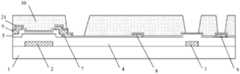
图16为本发明实施例的一种阵列基板的截面图。参照图16,所述阵列基板可以包括:FIG. 16 is a cross-sectional view of an array substrate according to an embodiment of the present invention. Referring to FIG. 16, the array substrate may include:
基板1;
形成在基板1上的栅电极2、栅线(图未示)和栅焊盘3;A
形成在栅电极2和栅线上的栅绝缘层4;a
形成在栅绝缘层4上的半导体层5、数据线8和数据焊盘9;A
形成在半导体层5上的源电极6和漏电极7;a
形成在源电极6、漏电极7、数据线8和半导体层5上的无机绝缘膜21;An inorganic insulating
形成在无机绝缘膜21上的有机绝缘膜10,无机绝缘膜21和有机绝缘膜10上形成有第一接触孔11;An organic insulating
形成在有机绝缘膜10上的像素电极12,像素电极12通过第一接触孔11与漏电极7电连接;A
形成在像素电极12和有机绝缘膜10上的保护膜13;a
形成在保护膜13上的公共电极16,公共电极16包括位于像素电极12上方的第一公共电极161和位于数据线8上方的第二公共电极162;A
在所述栅焊盘3上方形成的第二接触孔14和栅焊盘电极17,所述栅焊盘电极17通过所述第二接触孔14与所述栅焊盘3电连接;A
在所述数据焊盘9上方形成的第三接触孔15和数据焊盘电极18,所述数据焊盘电极18通过所述第三接触孔15与所述数据焊盘9电连接。A
根据本发明的实施例,通过将低介电常数(2.0~4.0)的有机绝缘膜10应用于阵列基板,来降低公共电极162和数据线8之间的寄生电容,从而能够降低数据线8上的信号延迟,改善显示质量。相对于现有技术中通过增加保护膜13的厚度来降低寄生电容,本发明实施例还能够减少工艺时间和降低制造成本。According to the embodiment of the present invention, the parasitic capacitance between the
根据本发明的实施例,由于采用了低介电常数的有机绝缘膜10,还可以通过减小像素电极12和数据线8之间的距离,来增加像素的开口率,其中,所述像素电极12与所述数据线8在沿平行于基板1的方向之间的距离可以减小到0~1μm。According to the embodiment of the present invention, since the organic insulating
另外,如果有机绝缘膜10和半导体层5接触,则在高温环境下,有机绝缘膜中10的离子异物会渗透到半导体层5,带来TFT中漏电流的增加。根据本发明的实施例,在有机绝缘膜10和半导体层5之间形成无机绝缘膜21作为缓冲层,所述缓冲层能够阻止有机绝缘膜10中的离子异物渗透到半导体层5,从而防止在高温下TFT中漏电流的产生。In addition, if the organic insulating
其中,所述有机绝缘膜10的材料可以采用聚丙烯酸,所述有机绝缘膜10的厚度为


本发明实施例中,数据线下方可以保留半导体层(如图13所示),也可以不保留半导体层(如图14所示);源电极和/或漏电极可以完全位于半导体层的上方(如图13所示),也可以延伸至半导体层之外的区域(如图14所示)。当源电极和/或漏电极延伸至半导体层之外的区域时,具有更好的接触效果。In the embodiment of the present invention, the semiconductor layer may be reserved under the data line (as shown in FIG. 13 ), or the semiconductor layer may not be reserved (as shown in FIG. 14 ); the source electrode and/or drain electrode may be completely located above the semiconductor layer (as shown in FIG. 14 ). As shown in FIG. 13 ), it may also extend to a region outside the semiconductor layer (as shown in FIG. 14 ). When the source electrode and/or the drain electrode extend to a region outside the semiconductor layer, it has a better contact effect.
本发明实施例中,半导体层5可以为普通硅半导体(本征半导体+掺杂半导体),也可以为有机半导体,还可以为氧化物半导体。In the embodiment of the present invention, the
本发明实施例中,公共电极16为狭缝状,像素电极12可以为板状,也可以为狭缝状。In the embodiment of the present invention, the
本发明实施例还提供一种显示装置,所述显示装置可以包括上述的任一种阵列基板。所述显示装置可以为:液晶面板、电子纸、手机、平板电脑、电视机、显示器、笔记本电脑、数码相框、导航仪等任何具有显示功能的产品或部件。An embodiment of the present invention also provides a display device, and the display device may include any one of the above-mentioned array substrates. The display device may be any product or component with a display function such as a liquid crystal panel, electronic paper, a mobile phone, a tablet computer, a television, a monitor, a notebook computer, a digital photo frame, a navigator, and the like.
以下给出上述阵列基板的制造方法。The manufacturing method of the above-mentioned array substrate is given below.
方法实施例1Method Example 1
步骤S11,提供一基板,在基板上形成栅线、栅电极和栅焊盘;Step S11, providing a substrate, forming gate lines, gate electrodes and gate pads on the substrate;
首先,可以采用溅射、热蒸发或其它成膜方法,在玻璃基板或其他类型的透明基板上面形成栅金属层,栅金属层可以采用铬(Cr)、钼(Mo)、铝(Al)、铜(Cu)、钨(W)、钕(Nd)及其合金,并且,栅金属层可以为一层或多层;然后,在栅金属层上形成光刻胶;其次,采用刻画有图形的掩膜板对光刻胶进行曝光和显影,形成光刻胶掩膜;再次,采用光刻胶掩膜对栅金属层进行刻蚀,形成栅线、栅电极和栅焊盘的图形;最后,剥离剩余的光刻胶。需要说明的是,本步骤中,在形成栅线、栅电极和栅焊盘的图形的同时,还可以形成公共电极线。First, sputtering, thermal evaporation or other film-forming methods can be used to form a gate metal layer on a glass substrate or other types of transparent substrates. The gate metal layer can be made of chromium (Cr), molybdenum (Mo), aluminum (Al), Copper (Cu), tungsten (W), neodymium (Nd) and their alloys, and the gate metal layer can be one or more layers; then, a photoresist is formed on the gate metal layer; secondly, a patterned The mask plate exposes and develops the photoresist to form a photoresist mask; again, the photoresist mask is used to etch the gate metal layer to form patterns of gate lines, gate electrodes and gate pads; finally, Strip remaining photoresist. It should be noted that, in this step, while forming the patterns of the gate lines, gate electrodes and gate pads, the common electrode lines can also be formed.
步骤S12,在完成步骤S11的基板上形成栅绝缘层;Step S12, forming a gate insulating layer on the substrate after step S11;
如图2所示,可以采用等离子体增强化学气相沉积(PECVD)等方法,在所述基板1上沉积厚度为的栅绝缘层4。其中,栅绝缘层4可以选用氧化物(例如SiOx)或者氮化物(例如SiNx)等材料。As shown in Figure 2, methods such as plasma-enhanced chemical vapor deposition (PECVD) can be used to deposit a thickness of The
步骤S13,在完成步骤S12的基板上形成半导体层;Step S13, forming a semiconductor layer on the substrate after step S12;
如图3所示,首先,可以采用PECVD等方法,在所述基板1上形成厚度为
步骤S14,在完成步骤S13的基板上形成源电极、漏电极、数据线和数据焊盘;Step S14, forming source electrodes, drain electrodes, data lines and data pads on the substrate after step S13;
如图4所示,首先,可以采用溅射、热蒸发或其它成膜方法,在所述基板1上面形成厚度为
步骤S15,在完成步骤S14的基板上形成无机绝缘膜;Step S15, forming an inorganic insulating film on the substrate after step S14;
如图5所示,可以采用PECVD等方法,在所述基板1上沉积厚度为
步骤S16,在完成步骤S15的基板上形成有机绝缘膜,并对有机绝缘膜进行构图;Step S16, forming an organic insulating film on the substrate after step S15, and patterning the organic insulating film;
如图6所示,首先,在所述基板1上形成厚度为
在本步骤中,如果有机绝缘膜10的厚度过小,则后续公共电极与数据线之间的寄生电容的减小效果(相对于无机绝缘膜)不明显;如果有机绝缘膜10的厚度过高,则层间段差部的坡度会增加,可能会带来像素电极断开等不良。In this step, if the thickness of the organic insulating
在本步骤中,固化处理的温度可以为230~260℃,时间可以为30~60分钟。固化温度如果低于230℃,进行后续工艺时由于保护膜的微固化,会产生污染以及膜翘起等不良;固化温度如果高于260℃,则可能造成有机绝缘膜10的变性,从而使得透过率低下。In this step, the temperature of the curing treatment may be 230-260° C., and the time may be 30-60 minutes. If the curing temperature is lower than 230°C, pollution and film warpage will occur due to the micro-curing of the protective film during subsequent processes; The pass rate is low.
步骤S17,刻蚀掉暴露的无机绝缘膜;Step S17, etching away the exposed inorganic insulating film;
如图7所示,以有机绝缘膜10作为掩膜,对暴露的无机绝缘膜21进行刻蚀,形成第一接触孔11,并暴露栅焊盘3区域的栅绝缘层4和数据焊盘9。As shown in FIG. 7, using the organic insulating
步骤S18,在完成步骤S17的基板上形成像素电极,所述像素电极通过所述第一接触孔与漏电极电连接;Step S18, forming a pixel electrode on the substrate after step S17, and the pixel electrode is electrically connected to the drain electrode through the first contact hole;
如图8所示,首先,可以采用磁控溅射、热蒸发或其它成膜方法,在所述基板1上形成厚度为
在本步骤中,如果像素电极12的厚度过低,则会使得其电阻过高;如果像素电极12的厚度过高,则会造成透过率低下。In this step, if the thickness of the
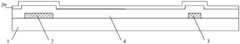
图9的左半部分是现有技术完成像素电极后的阵列基板的截面图,右半部分为本发明实施例完成像素电极后的阵列基板的截面图。如图9所示,在现有技术中,为避免像素电极12和数据线8之间的寄生电容给像素电极12的充电特性带来的影响,像素电极12与数据线8之间的距离d1需要做的较大,一般为2μm左右,这导致像素的开口率降低;而在本发明实施例中,由于采用了有机绝缘模10,则像素电极12和数据线8之间的距离d2做的较小时,像素电极和数据线之间的寄生电容也不会太大,因此,可以将所述d2减小到0~1μm,来增加像素的开口率。The left half of FIG. 9 is a cross-sectional view of the array substrate after the pixel electrodes are completed in the prior art, and the right half is a cross-sectional view of the array substrate after the pixel electrodes are completed in the embodiment of the present invention. As shown in FIG. 9 , in the prior art, in order to avoid the influence of the parasitic capacitance between the
步骤S19,在完成步骤S18的基板上形成保护膜,并对保护膜进行构图;Step S19, forming a protective film on the substrate after step S18, and patterning the protective film;
如图10所示,首先,可以采用PECVD等方法,在所述基板1上形成厚度为
在本步骤中,保护膜13的厚度低于

步骤S20,在完成步骤S19的基板上形成公共电极、栅焊盘电极和数据焊盘电极。Step S20 , forming a common electrode, a gate pad electrode and a data pad electrode on the substrate after step S19 .
如图16所示,首先,可以采用磁控溅射、热蒸发或其它成膜方法,在所述基板1上形成厚度为
其中,所述公共电极16包括位于像素电极12上方的第一公共电极161和位于数据线8上方的第二公共电极162,所述公共电极16为狭缝状。所述栅焊盘电极17通过所述第二接触孔14与所述栅焊盘3电连接,所述数据焊盘电极18通过所述第三接触孔15与所述数据焊盘9电连接Wherein, the
在本步骤中,如果公共电极16的厚度过低,则会使得其电阻过高;如果公共电极16的厚度过高,则会造成透过率低下。In this step, if the thickness of the
在本实施例中,第二公共电极162位于数据线8的上方,能够屏蔽像素电极12和数据线8之间的电磁场,以此能够减小彩色滤光片上黑矩阵的宽度,从而能够增加像素的开口率。In this embodiment, the second
方法实施例2Method Example 2
步骤S21,提供一基板,在基板上形成栅线、栅电极和栅焊盘;Step S21, providing a substrate, and forming gate lines, gate electrodes and gate pads on the substrate;
首先,可以采用溅射、热蒸发或其它成膜方法,在玻璃基板或其他类型的透明基板上面形成栅金属层,栅金属层可以采用铬(Cr)、钼(Mo)、铝(Al)、铜(Cu)、钨(W)、钕(Nd)及其合金,并且,栅金属层可以为一层或多层;然后,在栅金属层上形成光刻胶;其次,采用刻画有图形的掩膜板对光刻胶进行曝光和显影,形成光刻胶掩膜;再次,采用光刻胶掩膜对栅金属层进行刻蚀,形成栅线、栅电极和栅焊盘的图形;最后,剥离剩余的光刻胶。需要说明的是,本步骤中,在形成栅线、栅电极和栅焊盘的图形的同时,还可以形成公共电极线。First, sputtering, thermal evaporation or other film-forming methods can be used to form a gate metal layer on a glass substrate or other types of transparent substrates. The gate metal layer can be made of chromium (Cr), molybdenum (Mo), aluminum (Al), Copper (Cu), tungsten (W), neodymium (Nd) and their alloys, and the gate metal layer can be one or more layers; then, a photoresist is formed on the gate metal layer; secondly, a patterned The mask plate exposes and develops the photoresist to form a photoresist mask; again, the photoresist mask is used to etch the gate metal layer to form patterns of gate lines, gate electrodes and gate pads; finally, Strip remaining photoresist. It should be noted that, in this step, while forming the patterns of the gate lines, gate electrodes and gate pads, the common electrode lines can also be formed.
步骤S22,在完成步骤S21的基板上形成栅绝缘层;Step S22, forming a gate insulating layer on the substrate after step S21;
如图2所示,可以采用等离子体增强化学气相沉积(PECVD)等方法,在所述基板1上沉积厚度为
步骤S23,在完成步骤S22的基板上形成半导体材料层;Step S23, forming a semiconductor material layer on the substrate after step S22;
如图11所示,可以采用PECVD等方法,在所述基板1上形成厚度为
步骤S24,在完成步骤S23的基板上形成源漏金属层;Step S24, forming a source-drain metal layer on the substrate after step S23;
可以采用溅射、热蒸发或其它成膜方法,在所述基板1上面形成厚度为
步骤S25,在完成步骤S24的基板上形成光刻胶掩膜;Step S25, forming a photoresist mask on the substrate after step S24;
如图12所示,首先,在源漏金属层上形成光刻胶层19;其次,采用刻画有图形的灰色调或半色调掩膜板对光刻胶层19进行曝光和显影,形成包括光刻胶完全保留区域、光刻胶部分保留区域和光刻胶未保留区域的光刻胶掩膜。As shown in FIG. 12 , firstly, a
步骤S26,形成数据线和数据焊盘的图形;Step S26, forming a pattern of data lines and data pads;
如图13所示,采用光刻胶掩膜对光刻胶未保留区域的源漏金属层进行刻蚀,形成数据线8和数据焊盘9的图形。As shown in FIG. 13 , the photoresist mask is used to etch the source-drain metal layer in the region where the photoresist is not retained, to form patterns of
步骤S27,刻蚀光刻胶未保留区域的半导体材料层,并进行灰化工艺;Step S27, etching the semiconductor material layer in the region where the photoresist is not retained, and performing an ashing process;
如图14所示,首先,采用光刻胶掩膜对光刻胶未保留区域的半导体材料层20进行刻蚀,形成半导体层5的图形;然后,通过灰化工艺去除光刻胶部分保留区域的光刻胶,光刻胶完全保留区域的光刻胶变薄,形成新的光刻胶掩膜。As shown in Figure 14, at first, use photoresist mask to etch the
步骤S28,形成源电极和漏电极的图形;Step S28, forming patterns of source electrodes and drain electrodes;
如图15所示,首先,采用光刻胶掩膜刻蚀暴露的源漏金属层,形成源电极6和漏电极7的图形;然后,刻蚀掉源电极6和漏电极7之间的半导体层5的一部分,并剥离剩余的光刻胶,以此完成薄膜晶体管的沟道。其中,刻蚀掉源电极6和漏电极7之间的半导体层5的一部分,主要是指当半导体层5为本征半导体和掺杂半导体(欧姆接触层)构成的硅半导体结构时,应刻蚀掉源电极6和漏电极7之间的欧姆接触层;而当半导体层5为有机半导体或氧化物半导体时,刻蚀掉半导体层5的一部分是主要是由于刻蚀源漏金属层时的过刻所致,而不需刻意去刻蚀掉半导体层5的一部分,只需保证沟道区域的源漏金属层完全刻蚀掉即可。As shown in Figure 15, at first, adopt photoresist mask etching exposed source and drain metal layer, form the pattern of
在以下步骤中,虽然图中未示出,但是可以理解的是,在数据线8和数据焊盘9下方仍然保留了未刻蚀掉的半导体材料。In the following steps, although not shown in the figure, it can be understood that unetched semiconductor material still remains under the
步骤S29,在完成步骤S28的基板上形成无机绝缘膜;Step S29, forming an inorganic insulating film on the substrate after step S28;
如图5所示,可以采用PECVD等方法,在所述基板1上沉积厚度为
步骤S30,在完成步骤S29的基板上形成有机绝缘膜,并对有机绝缘膜进行构图;Step S30, forming an organic insulating film on the substrate after step S29, and patterning the organic insulating film;
如图6所示,首先,在所述基板1上形成厚度为
在本步骤中,如果有机绝缘膜10的厚度过小,则后续公共电极与数据线之间的寄生电容的减小效果(相对于无机绝缘膜)不明显;如果有机绝缘膜10的厚度过高,则层间段差部的坡度会增加,可能会带来像素电极断开等不良。In this step, if the thickness of the organic insulating
在本步骤中,固化处理的温度可以为230~260℃,时间可以为30~60分钟。固化温度如果低于230℃,进行后续工艺时由于保护膜的微固化,会产生污染以及膜翘起等不良;固化温度如果高于260℃,则可能造成有机绝缘膜10的变性,从而使得透过率低下。In this step, the temperature of the curing treatment may be 230-260° C., and the time may be 30-60 minutes. If the curing temperature is lower than 230°C, pollution and film warpage will occur due to the micro-curing of the protective film during subsequent processes; The pass rate is low.
步骤S31,刻蚀掉暴露的无机绝缘膜;Step S31, etching away the exposed inorganic insulating film;
如图7所示,以有机绝缘膜10作为掩膜,对暴露的无机绝缘膜21进行刻蚀,形成第一接触孔11,并暴露栅焊盘3区域的栅绝缘层4和数据焊盘9。As shown in FIG. 7, using the organic insulating
步骤S32,在完成步骤S31的基板上形成像素电极,所述像素电极通过所述第一接触孔与漏电极电连接;Step S32, forming a pixel electrode on the substrate after step S31, and the pixel electrode is electrically connected to the drain electrode through the first contact hole;
如图8所示,首先,可以采用磁控溅射、热蒸发或其它成膜方法,在所述基板1上形成厚度为
在本步骤中,如果像素电极12的厚度过低,则会使得其电阻过高;如果像素电极12的厚度过高,则会造成透过率低下。In this step, if the thickness of the
图9的左半部分是现有技术完成像素电极后的阵列基板的截面图,右半部分为本发明实施例完成像素电极后的阵列基板的截面图。如图9所示,在现有技术中,为避免像素电极12和数据线8之间的寄生电容给像素电极12的充电特性带来的影响,像素电极12与数据线8之间的距离d1需要做的较大,一般为2μm左右,这导致像素的开口率降低;而在本发明实施例中,由于采用了有机绝缘模10,则像素电极12和数据线8之间的距离d2做的较小时,像素电极和数据线之间的寄生电容也不会太大,因此,可以将所述d2减小到0~1μm,来增加像素的开口率。The left half of FIG. 9 is a cross-sectional view of the array substrate after the pixel electrodes are completed in the prior art, and the right half is a cross-sectional view of the array substrate after the pixel electrodes are completed in the embodiment of the present invention. As shown in FIG. 9 , in the prior art, in order to avoid the influence of the parasitic capacitance between the
步骤S33,在完成步骤S32的基板上形成保护膜,并对保护膜进行构图;Step S33, forming a protective film on the substrate after step S32, and patterning the protective film;
如图10所示,首先,可以采用PECVD等方法,在所述基板1上形成厚度为
在本步骤中,保护膜13的厚度低于时,存储电容(Cst)上升,会造成信号延迟增加;保护膜13的厚度高于
步骤S34,在完成步骤S33的基板上形成公共电极、栅焊盘电极和数据焊盘电极。Step S34 , forming a common electrode, a gate pad electrode and a data pad electrode on the substrate after step S33 .
如图16所示,首先,可以采用磁控溅射、热蒸发或其它成膜方法,在所述基板1上形成厚度为
其中,所述公共电极16包括位于像素电极12上方的第一公共电极161和位于数据线8上方的第二公共电极162,所述栅焊盘电极17通过所述第二接触孔14与所述栅焊盘3电连接,所述数据焊盘电极18通过所述第三接触孔15与所述数据焊盘9电连接Wherein, the
在本步骤中,如果公共电极16的厚度过低,则会使得其电阻过高;如果公共电极16的厚度过高,则会造成透过率低下。In this step, if the thickness of the
在本实施例中,第二公共电极162位于数据线8的上方,能够屏蔽像素电极12和数据线8之间的电磁场,以此能够减小彩色滤光片上黑矩阵的宽度,从而能够增加像素的开口率。另外,在形成半导体层5、源电极6和漏电极7时,由于采用了灰化工艺,还可以减少掩膜板数量,从而降低制造成本。In this embodiment, the second
最后应当说明的是,以上实施例仅用以说明本发明的技术方案而非限制,本领域的普通技术人员应当理解,可以对本发明的技术方案进行修改或者等同替换,而不脱离本发明技术方案的精神范围,其均应涵盖在本发明的权利要求范围当中。Finally, it should be noted that the above embodiments are only used to illustrate the technical solution of the present invention and not to limit it. Those of ordinary skill in the art should understand that the technical solution of the present invention can be modified or equivalently replaced without departing from the technical solution of the present invention. The spiritual scope of the invention should be included in the scope of the claims of the present invention.
Claims (19)


Priority Applications (2)
| Application Number | Priority Date | Filing Date | Title |
|---|---|---|---|
| CN2012101190080ACN102645808A (en) | 2012-04-20 | 2012-04-20 | Method for manufacturing array substrate, array substrate and display device |
| PCT/CN2012/083889WO2013155830A1 (en) | 2012-04-20 | 2012-10-31 | Method for manufacturing array substrate, array substrate, and display device |
Applications Claiming Priority (1)
| Application Number | Priority Date | Filing Date | Title |
|---|---|---|---|
| CN2012101190080ACN102645808A (en) | 2012-04-20 | 2012-04-20 | Method for manufacturing array substrate, array substrate and display device |
Publications (1)
| Publication Number | Publication Date |
|---|---|
| CN102645808Atrue CN102645808A (en) | 2012-08-22 |
Family
ID=46658715
Family Applications (1)
| Application Number | Title | Priority Date | Filing Date |
|---|---|---|---|
| CN2012101190080APendingCN102645808A (en) | 2012-04-20 | 2012-04-20 | Method for manufacturing array substrate, array substrate and display device |
Country Status (2)
| Country | Link |
|---|---|
| CN (1) | CN102645808A (en) |
| WO (1) | WO2013155830A1 (en) |
Cited By (20)
| Publication number | Priority date | Publication date | Assignee | Title |
|---|---|---|---|---|
| CN103219319A (en)* | 2013-04-26 | 2013-07-24 | 京东方科技集团股份有限公司 | Array substrate and manufacturing method thereof and display device |
| CN103325794A (en)* | 2013-05-30 | 2013-09-25 | 合肥京东方光电科技有限公司 | Array substrate, display device and method for manufacturing array substrate |
| CN103325792A (en)* | 2013-05-23 | 2013-09-25 | 合肥京东方光电科技有限公司 | Array substrate, preparation method and display device |
| CN103346160A (en)* | 2013-07-10 | 2013-10-09 | 京东方科技集团股份有限公司 | Array substrate and manufacturing method thereof and displaying device |
| CN103365012A (en)* | 2013-04-03 | 2013-10-23 | 友达光电股份有限公司 | Pixel structure and manufacturing method thereof |
| WO2013155845A1 (en)* | 2012-04-20 | 2013-10-24 | 京东方科技集团股份有限公司 | Method for manufacturing array substrate, array substrate, and display device |
| WO2013155830A1 (en)* | 2012-04-20 | 2013-10-24 | 京东方科技集团股份有限公司 | Method for manufacturing array substrate, array substrate, and display device |
| CN103439840A (en)* | 2013-08-30 | 2013-12-11 | 京东方科技集团股份有限公司 | Array substrate, display device and method for manufacturing array substrate |
| CN103560112A (en)* | 2013-11-12 | 2014-02-05 | 深圳市华星光电技术有限公司 | Method for manufacturing thin film transistor substrate and thin film transistor substrate manufactured through same |
| CN103943637A (en)* | 2014-04-10 | 2014-07-23 | 京东方科技集团股份有限公司 | Array substrate, method for manufacturing array substrate and display device |
| CN104766819A (en)* | 2014-01-06 | 2015-07-08 | 瀚宇彩晶股份有限公司 | Pixel substrate and manufacturing method thereof |
| CN105185789A (en)* | 2015-09-07 | 2015-12-23 | 昆山龙腾光电有限公司 | Fabrication method of array substrate, array substrate and liquid crystal display device |
| WO2016065852A1 (en)* | 2014-10-31 | 2016-05-06 | 京东方科技集团股份有限公司 | Coa substrate and manufacturing method thereof and display device |
| CN107636823A (en)* | 2016-07-25 | 2018-01-26 | 深圳市柔宇科技有限公司 | Manufacturing method of array substrate |
| WO2018196193A1 (en)* | 2017-04-24 | 2018-11-01 | 惠科股份有限公司 | Array substrate, manufacturing method therefor and display panel |
| CN110045852A (en)* | 2017-12-13 | 2019-07-23 | 乐金显示有限公司 | Display device and its manufacturing method with touch sensor |
| CN110112145A (en)* | 2015-01-21 | 2019-08-09 | 群创光电股份有限公司 | Display device |
| CN110310921A (en)* | 2019-07-09 | 2019-10-08 | 京东方科技集团股份有限公司 | A display substrate and its manufacturing method, a display panel and a display device |
| CN113867028A (en)* | 2021-10-09 | 2021-12-31 | 福建华佳彩有限公司 | Pixel structure with low touch load |
| CN114114763A (en)* | 2020-08-27 | 2022-03-01 | 合肥京东方显示技术有限公司 | Display substrate and display panel |
Families Citing this family (2)
| Publication number | Priority date | Publication date | Assignee | Title |
|---|---|---|---|---|
| CN104966721B (en)* | 2015-07-15 | 2018-10-02 | 京东方科技集团股份有限公司 | A kind of array substrate and preparation method thereof, display panel and display device |
| CN106298647B (en)* | 2016-08-31 | 2017-12-19 | 京东方科技集团股份有限公司 | A kind of array base palte and preparation method thereof, display panel and preparation method thereof |
Citations (5)
| Publication number | Priority date | Publication date | Assignee | Title |
|---|---|---|---|---|
| CN1369730A (en)* | 2001-01-29 | 2002-09-18 | 株式会社日立制作所 | Liquid crystal display |
| CN1395139A (en)* | 2001-07-02 | 2003-02-05 | 日本电气株式会社 | Plane internal switching type liquid crystal display and its manufacturing method |
| CN100373246C (en)* | 2001-11-15 | 2008-03-05 | Nec液晶技术株式会社 | Planar switch mode active matrix liquid crystal display device and manufacturing method thereof |
| CN101393363A (en)* | 2007-09-21 | 2009-03-25 | 北京京东方光电科技有限公司 | FFS type TFT-LCD array substrate structure and method for manufacturing same |
| US20090322974A1 (en)* | 2008-06-25 | 2009-12-31 | Samsung Electronics Co., Ltd. | Liquid crystal display and driving method thereof |
Family Cites Families (1)
| Publication number | Priority date | Publication date | Assignee | Title |
|---|---|---|---|---|
| CN102645808A (en)* | 2012-04-20 | 2012-08-22 | 京东方科技集团股份有限公司 | Method for manufacturing array substrate, array substrate and display device |
- 2012
- 2012-04-20CNCN2012101190080Apatent/CN102645808A/enactivePending
- 2012-10-31WOPCT/CN2012/083889patent/WO2013155830A1/enactiveApplication Filing
Patent Citations (5)
| Publication number | Priority date | Publication date | Assignee | Title |
|---|---|---|---|---|
| CN1369730A (en)* | 2001-01-29 | 2002-09-18 | 株式会社日立制作所 | Liquid crystal display |
| CN1395139A (en)* | 2001-07-02 | 2003-02-05 | 日本电气株式会社 | Plane internal switching type liquid crystal display and its manufacturing method |
| CN100373246C (en)* | 2001-11-15 | 2008-03-05 | Nec液晶技术株式会社 | Planar switch mode active matrix liquid crystal display device and manufacturing method thereof |
| CN101393363A (en)* | 2007-09-21 | 2009-03-25 | 北京京东方光电科技有限公司 | FFS type TFT-LCD array substrate structure and method for manufacturing same |
| US20090322974A1 (en)* | 2008-06-25 | 2009-12-31 | Samsung Electronics Co., Ltd. | Liquid crystal display and driving method thereof |
Cited By (42)
| Publication number | Priority date | Publication date | Assignee | Title |
|---|---|---|---|---|
| WO2013155845A1 (en)* | 2012-04-20 | 2013-10-24 | 京东方科技集团股份有限公司 | Method for manufacturing array substrate, array substrate, and display device |
| WO2013155830A1 (en)* | 2012-04-20 | 2013-10-24 | 京东方科技集团股份有限公司 | Method for manufacturing array substrate, array substrate, and display device |
| CN103365012A (en)* | 2013-04-03 | 2013-10-23 | 友达光电股份有限公司 | Pixel structure and manufacturing method thereof |
| WO2014172972A1 (en)* | 2013-04-26 | 2014-10-30 | 京东方科技集团股份有限公司 | Array substrate and manufacturing method therefor, and display apparatus |
| CN103219319A (en)* | 2013-04-26 | 2013-07-24 | 京东方科技集团股份有限公司 | Array substrate and manufacturing method thereof and display device |
| CN103219319B (en)* | 2013-04-26 | 2015-11-25 | 京东方科技集团股份有限公司 | Array base palte and preparation method thereof, display unit |
| CN103325792A (en)* | 2013-05-23 | 2013-09-25 | 合肥京东方光电科技有限公司 | Array substrate, preparation method and display device |
| WO2014187113A1 (en)* | 2013-05-23 | 2014-11-27 | 合肥京东方光电科技有限公司 | Array substrate, preparation method, and display apparatus |
| US20160246088A1 (en)* | 2013-05-30 | 2016-08-25 | Hefei Boe Optoelectronics Technology Co., Ltd. | Array substrate, display device and fabricating method of array substrate |
| CN103325794A (en)* | 2013-05-30 | 2013-09-25 | 合肥京东方光电科技有限公司 | Array substrate, display device and method for manufacturing array substrate |
| CN103346160A (en)* | 2013-07-10 | 2013-10-09 | 京东方科技集团股份有限公司 | Array substrate and manufacturing method thereof and displaying device |
| CN103346160B (en)* | 2013-07-10 | 2016-04-06 | 京东方科技集团股份有限公司 | Array base palte and preparation method thereof, display unit |
| CN103439840A (en)* | 2013-08-30 | 2013-12-11 | 京东方科技集团股份有限公司 | Array substrate, display device and method for manufacturing array substrate |
| US9759958B2 (en) | 2013-08-30 | 2017-09-12 | Boe Technology Group Co., Ltd. | Array substrate, display device and method for manufacturing array substrate |
| CN103439840B (en)* | 2013-08-30 | 2017-06-06 | 京东方科技集团股份有限公司 | A kind of manufacture method of array base palte, display device and array base palte |
| CN103560112A (en)* | 2013-11-12 | 2014-02-05 | 深圳市华星光电技术有限公司 | Method for manufacturing thin film transistor substrate and thin film transistor substrate manufactured through same |
| WO2015070463A1 (en)* | 2013-11-12 | 2015-05-21 | 深圳市华星光电技术有限公司 | Thin film transistor substrate manufacturing method, and thin film transistor substrate manufactured via same |
| GB2529987B (en)* | 2013-11-12 | 2020-08-19 | Shenzhen China Star Optoelect | Thin-film transistor upon a substrate and method of manufacturing therefor |
| CN103560112B (en)* | 2013-11-12 | 2015-11-18 | 深圳市华星光电技术有限公司 | The manufacture method of thin film transistor base plate and the thin film transistor base plate with the method manufacture |
| GB2529987A (en)* | 2013-11-12 | 2016-03-09 | Shenzhen China Star Optoelect | Thin Film transistor substrate manufacturing method, and thin film transistor substrate manufactured via same |
| CN104766819B (en)* | 2014-01-06 | 2017-12-08 | 瀚宇彩晶股份有限公司 | Pixel substrate and manufacturing method thereof |
| CN104766819A (en)* | 2014-01-06 | 2015-07-08 | 瀚宇彩晶股份有限公司 | Pixel substrate and manufacturing method thereof |
| US9553108B2 (en) | 2014-04-10 | 2017-01-24 | Boe Technology Group Co., Ltd. | Array substrate, method of manufacturing the same and display device |
| CN103943637A (en)* | 2014-04-10 | 2014-07-23 | 京东方科技集团股份有限公司 | Array substrate, method for manufacturing array substrate and display device |
| CN103943637B (en)* | 2014-04-10 | 2016-08-31 | 京东方科技集团股份有限公司 | A kind of array base palte, its manufacture method and display device |
| WO2016065852A1 (en)* | 2014-10-31 | 2016-05-06 | 京东方科技集团股份有限公司 | Coa substrate and manufacturing method thereof and display device |
| US10502994B2 (en) | 2014-10-31 | 2019-12-10 | Boe Technology Group Co., Ltd. | Color filter on array substrate and fabricating method thereof as well as a display device |
| CN110112145A (en)* | 2015-01-21 | 2019-08-09 | 群创光电股份有限公司 | Display device |
| CN110112145B (en)* | 2015-01-21 | 2023-08-29 | 群创光电股份有限公司 | display device |
| CN105185789A (en)* | 2015-09-07 | 2015-12-23 | 昆山龙腾光电有限公司 | Fabrication method of array substrate, array substrate and liquid crystal display device |
| CN107636823A (en)* | 2016-07-25 | 2018-01-26 | 深圳市柔宇科技有限公司 | Manufacturing method of array substrate |
| JP2019512873A (en)* | 2016-07-25 | 2019-05-16 | シェンジェン ロイオル テクノロジーズ カンパニー リミテッドShenzhen Royole Technologies Co., Ltd. | Array substrate manufacturing method |
| WO2018018351A1 (en)* | 2016-07-25 | 2018-02-01 | 深圳市柔宇科技有限公司 | Method for manufacturing array substrate |
| WO2018196193A1 (en)* | 2017-04-24 | 2018-11-01 | 惠科股份有限公司 | Array substrate, manufacturing method therefor and display panel |
| CN110045852A (en)* | 2017-12-13 | 2019-07-23 | 乐金显示有限公司 | Display device and its manufacturing method with touch sensor |
| CN110045852B (en)* | 2017-12-13 | 2022-07-26 | 乐金显示有限公司 | Display device having touch sensor and method of manufacturing the same |
| CN110310921A (en)* | 2019-07-09 | 2019-10-08 | 京东方科技集团股份有限公司 | A display substrate and its manufacturing method, a display panel and a display device |
| CN110310921B (en)* | 2019-07-09 | 2021-10-01 | 京东方科技集团股份有限公司 | A display substrate and its manufacturing method, a display panel and a display device |
| CN114114763A (en)* | 2020-08-27 | 2022-03-01 | 合肥京东方显示技术有限公司 | Display substrate and display panel |
| CN114114763B (en)* | 2020-08-27 | 2023-08-08 | 合肥京东方显示技术有限公司 | A display substrate and display panel |
| US12181761B2 (en) | 2020-08-27 | 2024-12-31 | Hefei Boe Display Technology Co., Ltd. | Display substrate and display panel for reducing crosstalk |
| CN113867028A (en)* | 2021-10-09 | 2021-12-31 | 福建华佳彩有限公司 | Pixel structure with low touch load |
Also Published As
| Publication number | Publication date |
|---|---|
| WO2013155830A1 (en) | 2013-10-24 |
Similar Documents
| Publication | Publication Date | Title |
|---|---|---|
| CN102645808A (en) | Method for manufacturing array substrate, array substrate and display device | |
| CN102707523A (en) | Manufacturing method of array substrate as well as array substrate and display device | |
| CN102881688B (en) | Array substrate, display panel and array substrate manufacturing method | |
| CN102629585B (en) | Display device, thin film transistor, array substrate and manufacturing method thereof | |
| CN103151359B (en) | A kind of display unit, array base palte and preparation method thereof | |
| US9859304B2 (en) | Manufacturing method of array substrate, array substrate and display device | |
| CN102903675B (en) | A TFT array substrate, manufacturing method and display device | |
| CN103236440B (en) | Thin-film transistor, array base palte and manufacture method thereof, display unit | |
| CN103439840B (en) | A kind of manufacture method of array base palte, display device and array base palte | |
| WO2017166341A1 (en) | Method for manufacturing tft substrate and manufactured tft substrate | |
| US9530807B2 (en) | Thin film transistor array substrate, manufacturing method thereof, and display device | |
| US8895334B2 (en) | Thin film transistor array substrate and method for manufacturing the same and electronic device | |
| CN102629584B (en) | Array substrate and manufacturing method thereof and display device | |
| CN104465672B (en) | Array substrate and display device | |
| WO2017012306A1 (en) | Method for manufacturing array substrate, array substrate, and display device | |
| CN202473925U (en) | Top gate type TFT (Thin Film Transistor) array substrate and display device | |
| CN104934443A (en) | Array substrate, manufacture method thereof, and display device | |
| CN103117248A (en) | Array substrate and manufacture method thereof and display device | |
| CN105448824A (en) | Array substrate and manufacturing method thereof as well as display device | |
| US9690146B2 (en) | Array substrate, its manufacturing method, and display device | |
| CN102931138B (en) | Array substrate and manufacturing method thereof and display device | |
| CN104779203B (en) | A kind of array base palte and its manufacture method, display device | |
| CN104020621B (en) | A kind of array base palte and preparation method thereof, display device | |
| CN106024705B (en) | Manufacturing method of TFT substrate | |
| US20120241746A1 (en) | Electrophoresis display and manufacturing method |
Legal Events
| Date | Code | Title | Description |
|---|---|---|---|
| C06 | Publication | ||
| PB01 | Publication | ||
| C10 | Entry into substantive examination | ||
| SE01 | Entry into force of request for substantive examination | ||
| C12 | Rejection of a patent application after its publication | ||
| RJ01 | Rejection of invention patent application after publication | Application publication date:20120822 |