CN102637676A - Light emitting diode package and backlight unit having the same - Google Patents
Light emitting diode package and backlight unit having the sameDownload PDFInfo
- Publication number
- CN102637676A CN102637676ACN2012100250154ACN201210025015ACN102637676ACN 102637676 ACN102637676 ACN 102637676ACN 2012100250154 ACN2012100250154 ACN 2012100250154ACN 201210025015 ACN201210025015 ACN 201210025015ACN 102637676 ACN102637676 ACN 102637676A
- Authority
- CN
- China
- Prior art keywords
- lead
- wire
- main
- son
- diode package
- Prior art date
- Legal status (The legal status is an assumption and is not a legal conclusion. Google has not performed a legal analysis and makes no representation as to the accuracy of the status listed.)
- Granted
Links
Images


Classifications
- H—ELECTRICITY
- H01—ELECTRIC ELEMENTS
- H01L—SEMICONDUCTOR DEVICES NOT COVERED BY CLASS H10
- H01L25/00—Assemblies consisting of a plurality of semiconductor or other solid state devices
- H01L25/16—Assemblies consisting of a plurality of semiconductor or other solid state devices the devices being of types provided for in two or more different subclasses of H10B, H10D, H10F, H10H, H10K or H10N, e.g. forming hybrid circuits
- H01L25/167—Assemblies consisting of a plurality of semiconductor or other solid state devices the devices being of types provided for in two or more different subclasses of H10B, H10D, H10F, H10H, H10K or H10N, e.g. forming hybrid circuits comprising optoelectronic devices, e.g. LED, photodiodes
- H—ELECTRICITY
- H10—SEMICONDUCTOR DEVICES; ELECTRIC SOLID-STATE DEVICES NOT OTHERWISE PROVIDED FOR
- H10H—INORGANIC LIGHT-EMITTING SEMICONDUCTOR DEVICES HAVING POTENTIAL BARRIERS
- H10H29/00—Integrated devices, or assemblies of multiple devices, comprising at least one light-emitting semiconductor element covered by group H10H20/00
- H10H29/20—Assemblies of multiple devices comprising at least one light-emitting semiconductor device covered by group H10H20/00
- H—ELECTRICITY
- H10—SEMICONDUCTOR DEVICES; ELECTRIC SOLID-STATE DEVICES NOT OTHERWISE PROVIDED FOR
- H10H—INORGANIC LIGHT-EMITTING SEMICONDUCTOR DEVICES HAVING POTENTIAL BARRIERS
- H10H20/00—Individual inorganic light-emitting semiconductor devices having potential barriers, e.g. light-emitting diodes [LED]
- H10H20/80—Constructional details
- H10H20/85—Packages
- H10H20/8506—Containers
- H—ELECTRICITY
- H10—SEMICONDUCTOR DEVICES; ELECTRIC SOLID-STATE DEVICES NOT OTHERWISE PROVIDED FOR
- H10H—INORGANIC LIGHT-EMITTING SEMICONDUCTOR DEVICES HAVING POTENTIAL BARRIERS
- H10H20/00—Individual inorganic light-emitting semiconductor devices having potential barriers, e.g. light-emitting diodes [LED]
- H10H20/80—Constructional details
- H10H20/85—Packages
- H10H20/857—Interconnections, e.g. lead-frames, bond wires or solder balls
- H—ELECTRICITY
- H10—SEMICONDUCTOR DEVICES; ELECTRIC SOLID-STATE DEVICES NOT OTHERWISE PROVIDED FOR
- H10H—INORGANIC LIGHT-EMITTING SEMICONDUCTOR DEVICES HAVING POTENTIAL BARRIERS
- H10H20/00—Individual inorganic light-emitting semiconductor devices having potential barriers, e.g. light-emitting diodes [LED]
- H10H20/80—Constructional details
- H10H20/85—Packages
- H10H20/858—Means for heat extraction or cooling
- H10H20/8582—Means for heat extraction or cooling characterised by their shape
- H—ELECTRICITY
- H01—ELECTRIC ELEMENTS
- H01L—SEMICONDUCTOR DEVICES NOT COVERED BY CLASS H10
- H01L2224/00—Indexing scheme for arrangements for connecting or disconnecting semiconductor or solid-state bodies and methods related thereto as covered by H01L24/00
- H01L2224/01—Means for bonding being attached to, or being formed on, the surface to be connected, e.g. chip-to-package, die-attach, "first-level" interconnects; Manufacturing methods related thereto
- H01L2224/42—Wire connectors; Manufacturing methods related thereto
- H01L2224/47—Structure, shape, material or disposition of the wire connectors after the connecting process
- H01L2224/48—Structure, shape, material or disposition of the wire connectors after the connecting process of an individual wire connector
- H01L2224/4805—Shape
- H01L2224/4809—Loop shape
- H01L2224/48091—Arched
- H—ELECTRICITY
- H01—ELECTRIC ELEMENTS
- H01L—SEMICONDUCTOR DEVICES NOT COVERED BY CLASS H10
- H01L2224/00—Indexing scheme for arrangements for connecting or disconnecting semiconductor or solid-state bodies and methods related thereto as covered by H01L24/00
- H01L2224/01—Means for bonding being attached to, or being formed on, the surface to be connected, e.g. chip-to-package, die-attach, "first-level" interconnects; Manufacturing methods related thereto
- H01L2224/42—Wire connectors; Manufacturing methods related thereto
- H01L2224/47—Structure, shape, material or disposition of the wire connectors after the connecting process
- H01L2224/49—Structure, shape, material or disposition of the wire connectors after the connecting process of a plurality of wire connectors
- H01L2224/491—Disposition
- H01L2224/49105—Connecting at different heights
- H01L2224/49107—Connecting at different heights on the semiconductor or solid-state body
Landscapes
- Engineering & Computer Science (AREA)
- Microelectronics & Electronic Packaging (AREA)
- Physics & Mathematics (AREA)
- Condensed Matter Physics & Semiconductors (AREA)
- General Physics & Mathematics (AREA)
- Computer Hardware Design (AREA)
- Power Engineering (AREA)
- Led Device Packages (AREA)
Abstract
Translated fromChinese
Description
Translated fromChinese本申请要求于2011年2月10日提交的第10-2011-0012008号韩国专利申请的优先权,为了所有目的,通过引用将该申请包含于此,就如同在此做了充分阐述一样。This application claims priority from Korean Patent Application No. 10-2011-0012008 filed on February 10, 2011, which is hereby incorporated by reference for all purposes as if fully set forth herein.
技术领域technical field
本发明的示例性实施例涉及一种发光二极管封装件及一种具有该发光二极管封装件的背光单元。更具体地讲,本发明的示例性实施例涉及一种受保护而免受静电放电电流损坏的发光二极管封装件及一种具有该发光二极管封装件的背光单元。Exemplary embodiments of the present invention relate to a light emitting diode package and a backlight unit having the light emitting diode package. More particularly, exemplary embodiments of the present invention relate to a light emitting diode package protected from electrostatic discharge current and a backlight unit having the light emitting diode package.
背景技术Background technique
由于显示面板为非发射装置,所以诸如液晶显示器的非发射显示设备包括背光单元以向显示面板提供光来显示图像。近来,背光单元使用发光二极管封装件来代替冷阴极荧光灯,以改善颜色再现性同时降低功耗。Since the display panel is a non-emissive device, a non-emissive display device such as a liquid crystal display includes a backlight unit to provide light to the display panel to display images. Recently, backlight units use light emitting diode packages instead of cold cathode fluorescent lamps to improve color reproducibility while reducing power consumption.
发光二极管封装件可以包括作为半导体装置的LED(发光二极管),以响应于施加的驱动电压来产生光。LED基于化合物半导体的特性通过使电子和空穴在其中复合而工作,从而产生光。The light emitting diode package may include an LED (Light Emitting Diode) as a semiconductor device to generate light in response to an applied driving voltage. LEDs work by recombining electrons and holes therein based on the properties of compound semiconductors, thereby generating light.
然而,LED会因在释放静电(通常称作静电放电;ESD)时产生的放电电流而损坏,这被称作“静电破坏”。通常,为了保护LED免受放电电流的损坏,发光二极管封装件包括瞬态电压抑制二极管或齐纳二极管。However, LEDs can be damaged by discharge current generated when static electricity is discharged (commonly called electrostatic discharge; ESD), which is called "electrostatic destruction". Generally, in order to protect the LED from being damaged by the discharge current, the light emitting diode package includes a transient voltage suppressor diode or a Zener diode.
在该背景技术部分中公开的以上信息仅用于加强对本发明背景的理解,因此它可包含对本领域普通技术人员而言不构成现有技术也不是现有技术会建议的内容的任何部分的信息。The above information disclosed in this Background section is only for enhancement of understanding of the background of the invention and therefore it may contain information that does not form any part of the prior art nor would it suggest prior art to a person of ordinary skill in the art .
发明内容Contents of the invention
本发明的示例性实施例提供了一种发光二极管封装件,该发光二极管封装件可以得到保护而免受在发生静电放电时产生的放电电流的损坏。Exemplary embodiments of the present invention provide a light emitting diode package that can be protected from damage by discharge current generated when electrostatic discharge occurs.
本发明的示例性实施例还提供了一种具有该发光二极管封装件的背光单元。Exemplary embodiments of the present invention also provide a backlight unit having the light emitting diode package.
在下面的描述中将阐述本发明的附加特征,本发明的附加特征通过该描述而部分地清楚,或者可以通过本发明的实践而获知。Additional features of the invention will be set forth in the description which follows, and in part will be apparent from the description, or may be learned by practice of the invention.
本发明的示例性实施例公开了一种包括发光二极管的发光二极管封装件。发光二极管包括第一电极和第二电极并响应于驱动电压产生光。第一主引线连接到第一电极,第二主引线连接到第二电极,发光二极管设置在固定有第一主引线和第二主引线的主体部分上。发光二极管封装件包括第一子引线和第二子引线,第一子引线具有连接到第一主引线的一个端部,第二子引线具有连接到第二主引线的一个端部和与第一子引线的相对端部分隔开同时面对第一子引线的相对端部的相对端部。第二子引线与第一子引线一起释放静电。Exemplary embodiments of the present invention disclose a light emitting diode package including a light emitting diode. A light emitting diode includes a first electrode and a second electrode and generates light in response to a driving voltage. The first main lead is connected to the first electrode, the second main lead is connected to the second electrode, and the light emitting diode is arranged on the main body portion where the first main lead and the second main lead are fixed. The light emitting diode package includes a first sub-lead having one end connected to the first main lead, and a second sub-lead having one end connected to the second main lead and a second sub-lead connected to the first main lead. The opposite ends of the sub-leads are spaced apart while facing opposite ends of the opposite ends of the first sub-lead. The second sub-lead discharges static electricity together with the first sub-lead.
本发明的示例性实施例还公开了一种背光单元,该背光单元包括基体构件、安装在基体构件上以产生光的多个发光二极管封装件和将驱动电压提供给发光二极管封装件的信号线。多个发光二极管封装件可以包括具有上述结构的发光二极管封装件中的至少一个。Exemplary embodiments of the present invention also disclose a backlight unit including a base member, a plurality of light emitting diode packages mounted on the base member to generate light, and a signal line supplying a driving voltage to the light emitting diode packages . The plurality of light emitting diode packages may include at least one of the light emitting diode packages having the above structure.
将理解的是,前面的总体描述和下面的详细描述是示例性的和解释性的,并意图提供对所要求保护的本发明的进一步解释。It is to be understood that both the foregoing general description and the following detailed description are exemplary and explanatory and are intended to provide further explanation of the invention as claimed.
附图说明Description of drawings
包括附图以提供对本发明的进一步理解,附图包含在本说明书中并构成本说明书的一部分,且附图示出本发明的实施例并与描述一起用于解释本发明的原理。The accompanying drawings are included to provide a further understanding of the invention, are incorporated in and constitute a part of this specification, and illustrate embodiments of the invention and together with the description serve to explain the principle of the invention.
图1是示出根据本发明一个实施例的发光二极管封装件的平面图。FIG. 1 is a plan view illustrating a light emitting diode package according to one embodiment of the present invention.
图2是示出图1中示出的发光二极管封装件的侧视图。FIG. 2 is a side view showing the light emitting diode package shown in FIG. 1 .
图3是沿图1中的线I-I′截取的剖视图。FIG. 3 is a cross-sectional view taken along line II' in FIG. 1 .
图4是示出图1中的发光二极管的剖视图。FIG. 4 is a cross-sectional view illustrating the light emitting diode in FIG. 1 .
图5是示出根据本发明另一实施例的发光二极管封装件的侧视图。FIG. 5 is a side view illustrating a light emitting diode package according to another embodiment of the present invention.
图6是示出根据本发明又一实施例的发光二极管封装件的侧视图。FIG. 6 is a side view illustrating a light emitting diode package according to still another embodiment of the present invention.
图7是沿图6中的线II-II′截取的剖视图。FIG. 7 is a cross-sectional view taken along line II-II' in FIG. 6 .
图8是示出根据本发明再一实施例的发光二极管封装件的平面图。FIG. 8 is a plan view illustrating a light emitting diode package according to still another embodiment of the present invention.
图9是沿图8中的线III-III′截取的剖视图。FIG. 9 is a cross-sectional view taken along line III-III' in FIG. 8 .
图10是示出根据本发明再一实施例的发光二极管封装件的平面图。FIG. 10 is a plan view illustrating a light emitting diode package according to still another embodiment of the present invention.
图11是示出根据本发明一个实施例的包括发光二极管封装件的背光单元的平面图。FIG. 11 is a plan view illustrating a backlight unit including a light emitting diode package according to one embodiment of the present invention.
图12是示出根据本发明另一实施例的包括发光二极管封装件的背光单元的平面图。FIG. 12 is a plan view illustrating a backlight unit including a light emitting diode package according to another embodiment of the present invention.
图13是示出本发明又一实施例的背光单元的侧视图。FIG. 13 is a side view showing a backlight unit according to still another embodiment of the present invention.
具体实施方式Detailed ways
在下文中,将参照附图更详细地描述本发明的示例性实施例。然而,本发明不限于下面的实施例,而是包括各种应用和修改。提供下面的实施例以使本发明中公开的技术精神清楚,并将本发明的技术精神充分地传达给本领域中具有一般知识和技能的人员。因此,本发明的范围不应局限于下面的实施例。Hereinafter, exemplary embodiments of the present invention will be described in more detail with reference to the accompanying drawings. However, the present invention is not limited to the following embodiments but includes various applications and modifications. The following examples are provided to clarify the technical spirit disclosed in the present invention and to fully convey the technical spirit of the present invention to those having ordinary knowledge and skills in the art. Therefore, the scope of the present invention should not be limited to the following examples.
当描述每个附图时,相似的标记表示相似的组件。此外,为了准确的解释或强调,简化或夸大与下面的实施例一起的附图的层和区域的尺寸,并且相同的标记表示相同的组件。为了解释各种组件的目的,使用术语“第一”和“第二”,并且组件不受术语“第一”和“第二”的限制。使用术语“第一”和“第二”仅用来将一个组件与另一组件区分开来。例如,在不偏离本发明的范围的情况下,可以将第一组件命名为第二组件。相似地,可以将第二组件命名为第一组件。除非在上下文中单数的含义明确地不同于复数的含义,否则说明书中单数的表达包括复数的含义。When describing each figure, like numerals refer to like components. Also, the dimensions of layers and regions of the drawings together with the following embodiments are simplified or exaggerated for accurate explanation or emphasis, and the same symbols denote the same components. The terms 'first' and 'second' are used for the purpose of explaining various components, and components are not limited by the terms 'first' and 'second'. The terms "first" and "second" are used only to distinguish one component from another. For example, a first component may be named a second component without departing from the scope of the present invention. Similarly, a second component can be named a first component. Expressions of the singular in the specification include the meaning of the plural unless the meaning of the singular is clearly different from the meaning of the plural in the context.
在下面的描述中,术语“包括”或“具有”可以表示说明书中描述的特征、数量、步骤、操作、组件、部件或它们的组合的存在,可以不排除另一特征、另一数量、另一步骤、另一操作、另一组件、另一部件或它们的组合的存在或附加。此外,当层、膜、区域或板被称作形成在另一层、另一膜、另一区域或另一板上时,该层、膜、区域或板可以直接形成在另一层、另一膜、另一区域或另一板上,或者第三层、第三膜、第三区域或第三板可以设置在该层、膜、区域或板与另一层、另一膜、另一区域或另一板之间。当层、膜、区域或板被称作形成在另一层、另一膜、另一区域或另一板之下时,该层、膜、区域或板可以直接形成在另一层、另一膜、另一区域或另一板之下,或者第三层、第三膜、第三区域或第三板可以设置在该层、膜、区域或板与另一层、另一膜、另一区域或另一板之间。相反,当元件被称作“直接在”另一元件“上”、“直接在”另一元件“之下”或“直接连接到”另一元件时,不存在中间元件。将理解的是,为了本公开的目的,“...中的至少一个”将被解释为表示相应表述之前列举的元件的任何组合,包括多个列举的元件的组合。例如,“X、Y和Z中的至少一个”将被解释为表示仅X、仅Y、仅Z或X、Y和Z中的两项或更多项的任意组合(例如,XYZ、XYY、XZ、YZ)。In the following description, the term "comprises" or "has" may indicate the presence of features, quantities, steps, operations, components, parts or combinations thereof described in the specification, and may not exclude another feature, another quantity, another The presence or addition of a step, another operation, another component, another part, or a combination thereof. Furthermore, when a layer, film, region or plate is referred to as being formed on another layer, another film, another region or another plate, the layer, film, region or plate may be directly formed on another layer, another film, another region or plate. A film, another region or another plate, or a third layer, third film, third region or third plate may be disposed on the layer, film, region or plate in conjunction with another layer, another film, another region or between another board. When a layer, film, region or plate is said to be formed under another layer, film, region or plate, the layer, film, region or plate may be formed directly under another layer, another film, another region or plate Underneath the film, another region or another plate, or a third layer, third film, third region or third plate may be disposed between the layer, film, region or plate and another layer, another film, another region or between another board. In contrast, when an element is referred to as being "directly on," "directly under" or "directly connected to" another element, there are no intervening elements present. It will be understood that for the purposes of this disclosure, "at least one of" will be construed to mean any combination of listed elements preceding the corresponding expression, including combinations of multiples of the listed elements. For example, "at least one of X, Y, and Z" will be interpreted to mean only X, only Y, only Z, or any combination of two or more of X, Y, and Z (e.g., XYZ, XYY, XZ, YZ).
在下文中,将参照附图更详细地描述本发明的示例性实施例。Hereinafter, exemplary embodiments of the present invention will be described in more detail with reference to the accompanying drawings.
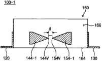
图1是示出根据本发明一个实施例的发光二极管封装件的平面图,图2是示出图1中示出的发光二极管封装件的侧视图。图3是沿图1中的线I-I′截取的剖视图,图4是示出构成图1中的发光二极管封装件的发光二极管的剖视图。FIG. 1 is a plan view showing a light emitting diode package according to one embodiment of the present invention, and FIG. 2 is a side view showing the light emitting diode package shown in FIG. 1 . 3 is a cross-sectional view taken along line II' in FIG. 1, and FIG. 4 is a cross-sectional view illustrating light emitting diodes constituting the light emitting diode package in FIG. 1. Referring to FIG.
参照图1至图4,发光二极管封装件100包括发光二极管110、第一主引线120、第二主引线130、主体部分160、第一子引线140和第二子引线150。Referring to FIGS. 1 to 4 , the light
发光二极管110响应于通过第一电极111和第二电极112施加到其的驱动电压产生光。发光二极管110具有堆叠结构,在该堆叠结构中,N型半导体层、有源层和P型半导体层顺序地堆叠。在该结构中,如果驱动电压被施加到发光二极管110,则电子和空穴在移动的同时彼此复合,从而产生光。The
在下文中,将参照图4更详细地描述发光二极管110。图4代表性地示出构成发光二极管封装件100的一个发光二极管。Hereinafter, the
如图4中所示,发光二极管110包括顺序地堆叠在基底113上的N型半导体层114、有源层115和P型半导体层116。此外,发光二极管110包括连接到P型半导体层116的P型电极111(第一电极)和连接到N型半导体层114的N型电极112(第二电极)。As shown in FIG. 4 , the
基底113包括透明材料,所述透明材料包括蓝宝石(Al2O3)。此外,基底113可以包括氧化锌(ZnO)、氮化镓(GaN)、碳化硅(SiC)、氮化铝(AlN)等。The substrate 113 includes a transparent material including sapphire (Al2 O3 ). In addition, the substrate 113 may include zinc oxide (ZnO), gallium nitride (GaN), silicon carbide (SiC), aluminum nitride (AlN), or the like.
N型半导体层114可以包括掺杂有N型导电杂质的N型氮化物半导体层,诸如GaN或GaN/AlGaN。P型半导体层116可以包括掺杂有P型导电杂质的P型氮化物半导体层,诸如GaN或GaN/AlGaN。有源层115可以包括具有多量子阱(MQW)结构的InGaN/GaN层。The N-type semiconductor layer 114 may include an N-type nitride semiconductor layer doped with N-type conductive impurities, such as GaN or GaN/AlGaN. The P-type semiconductor layer 116 may include a P-type nitride semiconductor layer doped with P-type conductive impurities, such as GaN or GaN/AlGaN. The active layer 115 may include an InGaN/GaN layer having a multiple quantum well (MQW) structure.
如果通过台面蚀刻工艺将P型半导体层116和有源层115的部分去除,则N型半导体层114的顶表面的部分暴露于外部。在这种情况下,将第一电极111设置在P型半导体层116上,将第二电极112设置在N型半导体层114的通过台面蚀刻工艺暴露于外部的顶表面上。If portions of the P-type semiconductor layer 116 and the active layer 115 are removed through a mesa etching process, a portion of the top surface of the N-type semiconductor layer 114 is exposed to the outside. In this case, the first electrode 111 is disposed on the P-type semiconductor layer 116, and the second electrode 112 is disposed on the top surface of the N-type semiconductor layer 114 exposed to the outside through the mesa etching process.
第一主引线120连接到发光二极管110的第一电极111,第二主引线130连接到发光二极管110的第二电极112。从外部施加的驱动电压通过第一主引线120提供给发光二极管110,降低的驱动电压从第二主引线130引出。换句话说,在发光二极管110中,通过第一主引线120将第一电压提供给第一电极111,通过第二主引线130将比第一电压低的第二电压提供给第二电极112。在这种情况下,第一电压与第二电压之间的差与驱动电压降低的幅度相等。The first
主体部分160将发光二极管110安装在其上,并将第一主引线120和第二主引线130固定到主体部分160。主体部分160可以包括树脂材料。The
如图1至图3中所示,主体部分160包括:安装表面162,发光二极管110安装在安装表面162上;底表面164,背对安装表面162设置;以及外部侧表面166,从底表面164弯曲并延伸。可以通过树脂粘合片(未示出)或导电粘合片(未示出)将发光二极管110安装在安装表面162上。As shown in FIGS. 1 to 3 , the
如图1至图3中所示,当底表面164具有矩形形状时,外部侧表面166可以分为四个区域(见图10)。此外,底表面164的面积可以比安装表面162的面积大,外部侧表面166可以按照比安装表面162与底表面164之间的距离长的长度延伸。如果主体部分160还包括从安装表面162弯曲并延伸的内部侧表面168,则主体部分160包括围绕发光二极管110的侧壁160w。成型构件可以填充在由内部侧表面168和外部侧表面166限定的空间中以保护发光二极管110。As shown in FIGS. 1 to 3 , when the
主引线120和130可以分别穿过主体部分160的部分。第一主引线120的一个端部和第二主引线130的一个端部暴露在安装表面162上,第一主引线120的从第一主引线120的所述一个端部延伸的相对端部和第二主引线130的从第二主引线130的所述一个端部延伸的相对端部从主体部分160突出。The main leads 120 and 130 may respectively pass through portions of the
例如,如图1和图3中所示,第一主引线120和第二主引线130中的每个穿过侧壁160w,每个相对端部从外部侧表面166突出。For example, as shown in FIGS. 1 and 3 , each of the first
在这种情况下,第一电极111可以通过使用第一线w1连接到第一主引线120的暴露在安装表面162上的所述一个端部,第二电极112可以通过使用第二线w2连接到第二主引线130的所述一个端部。同时,为了解释的目的,提供了以上的连接方案。因此,如果对图4中的发光二极管110进行修改,则主引线120和130可以通过其他连接方案连接到电极111和112。In this case, the first electrode 111 may be connected to the one end portion of the first
发光二极管110会因在发生静电放电时(即,当放电电流流过时)产生的热而损坏,这被称作“静电破坏”。通常,发光二极管110对小于2kV的放电电压下流过的放电电流具有耐受性。然而,对于2kV或更高的放电电压下流过的放电电流,在发光二极管110中发生静电破坏。为了防止静电破坏,发光二极管封装件100包括第一子引线140和第二子引线150。The
第一子引线140和第二子引线150分别连接到第一主引线120和第二主引线130。更具体地讲,参照图1至图3,第一子引线140的一个端部连接到第一主引线120,第二子引线150的一个端部连接到第二主引线130。第一子引线140和第二子引线150的相对端部以预定距离d彼此分隔开,同时彼此面对。The
在这种情况下,第一子引线140和第二子引线150的相对端部优选地从主体部分160突出。因此,静电放电可被引导到主体部分160的外部。In this case, opposite end portions of the
第一子引线140包括第一固定引线部分142和从第一固定引线部分142延伸的第一放电引线部分144。第一固定引线部分142的一端连接到第一主引线120,第一固定引线部分142的相对端暴露在外部侧表面166的外面。此外,第一放电引线部分144连接到第一固定引线部分142并从主体部分160突出。The
第二子引线150可以具有与第一子引线140的结构对应的结构。换句话说,第二子引线150包括第二固定引线部分152和从第二固定引线部分152延伸的第二放电引线部分154。第二固定引线部分152的一端连接到第二主引线130,第二固定引线部分152的相对端暴露在外部侧表面166的外面。此外,第二放电引线部分154连接到第二固定引线部分152并从主体部分160突出。The
如图1和图2中所示,第一放电引线部分144和第二放电引线部分154可以接触外部侧表面166。因此,当处理发光二极管封装件100时,可以防止第一放电引线部分144与第一固定引线部分142断开并防止第二放电引线部分154与第二固定引线部分152断开。As shown in FIGS. 1 and 2 , the first
在这种情况下,第一放电引线部分144和第二放电引线部分154在外部侧表面166上可以具有多边形形状。同时,虽然图2示出第一放电引线部分144和第二放电引线部分154在外部侧表面166上具有矩形形状,但可以对第一放电引线部分144和第二放电引线部分154的形状和面积进行修改。In this case, the first
第一放电引线部分144和第二放电引线部分154以预定的距离d彼此分开,同时彼此面对。根据下面的等式1,确定发生静电放电的临界放电电压。换句话说,当存储的负电荷与正电荷之间的电势差大于临界放电电压时,发生静电放电。The first
等式1Equation 1
Vc={(3000×p×d)+1350}Vc={(3000×p×d)+1350}
在等式1中,Vc是临界放电电压(单位为伏特(V)),p是大气压(单位是工程大气压(atm)),d是第一放电引线部分144和第二放电引线部分154之间的距离(单位为毫米(mm))。例如,当在1atm的大气压下,距离d为大约100μm时,临界放电电压为大约1650V。因此,当距离d为大约100μm时,且当存储的负电荷与正电荷之间的电势差为大约1650V或更大(即,放电电压为1650V或更大)时,发生ESD。换句话说,当距离d为大约100μm时,且当负电荷与正电荷之间的电势差为大约1650V或更大时,在第一放电引线部分144和第二放电引线部分154之间的介质(例如,空气)中发生介电击穿,放电电流流过该介质。In Equation 1, Vc is the critical discharge voltage (in volts (V)), p is the atmospheric pressure (in engineering atmospheric pressure (atm)), and d is the voltage between the first
在这种情况下,第一放电引线部分144和第二放电引线部分154之间的距离d优选地在大约50μm至大约1mm的范围内。如果第一放电引线部分144和第二放电引线部分154之间的距离d小于大约50μm,则静电放电过多地发生。如果第一放电引线部分144和第二放电引线部分154之间的距离超过大约1mm,则发光二极管110中会发生静电破坏。In this case, the distance d between the first
图5是示出根据本发明另一实施例的发光二极管封装件的侧视图。在下文中,将参照图5描述根据另一实施例的发光二极管封装件,但将不对与图1至图4中的结构和组件相同的结构和组件进行进一步的描述,以避免冗余。FIG. 5 is a side view illustrating a light emitting diode package according to another embodiment of the present invention. Hereinafter, a light emitting diode package according to another embodiment will be described with reference to FIG. 5 , but the same structures and components as those in FIGS. 1 to 4 will not be further described to avoid redundancy.
与图1至图4中示出的发光二极管封装件100相似,根据本实施例的发光二极管封装件100-1包括发光二极管110、第一主引线120、第二主引线130、主体部分160、第一子引线140和第二子引线150。此外,第一子引线140和第二子引线150中的每个可以包括固定引线部分以及设置在主体部分160的外部侧表面166上并具有多边形形状的放电引线部分。Similar to the light emitting
如图5中所示,第一子引线140包括在外部侧表面166上具有五边形形状的第一放电引线部分144-1,第二子引线150包括在外部侧表面166上具有五边形形状的第二放电引线部分154-1。此外,第一放电引线部分144-1和第二放电引线部分154-1可以接触外部侧表面166。As shown in FIG. 5 , the
在这种情况下,优选地,构成具有多边形形状的第一放电引线部分144-1的多个顶角中的具有最小顶角角度的顶角面对构成具有多边形形状的第二放电引线部分154-1的多个顶角中的具有最小角度的顶角。如图5中所示,如果第一放电引线部分144-1中具有最小顶角角度的顶角144V面对第二放电引线部分154-1中具有最小顶角角度的顶角154V,则电场集中,并且临界放电电压降低。In this case, preferably, the vertex angle having the smallest vertex angle among the plurality of vertex corners constituting the first discharge lead portion 144-1 having a polygonal shape faces the second
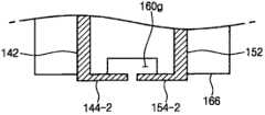
图6是示出根据本发明又一实施例的发光二极管封装件的侧视图,图描述,以避免冗余。FIG. 6 is a side view showing a light emitting diode package according to still another embodiment of the present invention, and the drawing is described to avoid redundancy.
如图6和图7中所示,在根据本实施例的发光二极管封装件100-2中,第一放电引线部分144-2和第二引线放电部分154-2的至少一部分接触外部侧表面166。As shown in FIG. 6 and FIG. 7, in the light emitting diode package 100-2 according to the present embodiment, at least a part of the first discharge lead portion 144-2 and the second lead discharge portion 154-2 contact the
在这种情况下,主体部分160包括形成在外部侧表面166的预定区域处的槽160g。所述预定区域至少包括与第一放电引线部分144-2的端部对应的区域以及与第二放电引线部分154-2的面对第一放电引线部分144-2的所述端部的端部对应的区域。第一放电引线部分144-2和第二放电引线部分154-2的彼此面对的端部不接触外部侧表面166。In this case, the
因此,由于第一放电引线部分144-2的至少一部分和第二放电引线部分154-2的至少一部分与外部侧表面166接触,所以可以防止第一放电引线部分144-2和第二放电引线部分154-2与第一固定引线部分142和第二固定引线部分152断开。Therefore, since at least a portion of the first discharge lead portion 144-2 and at least a portion of the second discharge lead portion 154-2 are in contact with the
此外,槽160g提供了允许第一放电引线部分144-2和第二放电引线部分154-2的彼此面对的端部与空气接触的空间,从而降低了临界放电电压。In addition, the
图8是示出根据本发明再一实施例的发光二极管封装件的平面图,图9是沿图8中的线III-III′截取的剖视图。在下文中,将参照图8和图9描述根据本实施例的发光二极管封装件。然而,将不对与图1至图7中的结构和组件相同的结构和组件进行进一步的描述,以避免冗余。8 is a plan view illustrating a light emitting diode package according to still another embodiment of the present invention, and FIG. 9 is a cross-sectional view taken along line III-III' in FIG. 8 . Hereinafter, a light emitting diode package according to the present embodiment will be described with reference to FIGS. 8 and 9 . However, the same structures and components as those in FIGS. 1 to 7 will not be further described to avoid redundancy.
根据本实施例的发光二极管封装件100-3还包括将发光二极管110产生的热排放到外部的散热器HS。The light emitting diode package 100-3 according to the present embodiment further includes a heat sink HS that discharges heat generated by the
如图8和图9中所示,主体部分160包括从安装表面162延伸到底表面164的通孔160t。通孔160t可以具有各种形状。例如,如图9中所示,沿图8中的线III-III′截取的截面可以具有梯形形状,与安装表面162平行地截取的截面可以具有圆形形状或多边形形状。As shown in FIGS. 8 and 9 , the
散热器HS设置在通孔160t中。散热器HS可以包括表现出优异的导热率的金属。优选地,散热器HS可以具有与通孔160t的形状相同的形状。The heat sink HS is disposed in the through hole 160t. The heat sink HS may include metal exhibiting excellent thermal conductivity. Preferably, the heat sink HS may have the same shape as that of the through hole 160t.
在这种情况下,散热器HS的一个表面HS-162可以与安装表面162齐平。发光二极管110可以安装在散热器HS的表面HS-162上以提高散热效率。此外,背对表面HS-162的相对表面可以与底表面164齐平。In this case, one surface HS- 162 of the heat sink HS may be flush with the mounting
图10是示出根据本发明再一实施例的发光二极管封装件的平面图。在下文中,将参照图10描述根据本实施例的发光二极管封装件。然而,将不对与图1至图9中的结构和组件相同的结构和组件进行进一步的描述,以避免冗余。FIG. 10 is a plan view illustrating a light emitting diode package according to still another embodiment of the present invention. Hereinafter, the light emitting diode package according to the present embodiment will be described with reference to FIG. 10 . However, the same structures and components as those in FIGS. 1 to 9 will not be further described to avoid redundancy.
根据本实施例的发光二极管封装件100-4包括多个第一子引线140和多个第二子引线150。第一子引线140的数量与第二子引线150的数量相等。在这种情况下,每个第一子引线140的一个端部连接到第一主引线120,每个子引线150的一个端部连接到第二主引线130。此外,第一子引线140的相对端部一一对应地面对第二子引线150的相对端部。在这种发光二极管封装件100-4中,ESD可以发生在两点或更多点处。The light emitting diode package 100 - 4 according to the present embodiment includes a plurality of
如图10中所示,第一子引线140和第二子引线150的相对端部可以从主体部分160突出。当发光二极管封装件100-4的底表面164(见图2)具有矩形形状时,并且当从底表面164弯曲并延伸的外部侧表面166分为四个区域166-1、166-2、166-3和166-4时,一对子引线140和150的相对端部可以从第一区域166-1突出,另一对子引线140和150的相对端部可以从背对第一区域166-1的第二区域166-2突出。As shown in FIG. 10 , opposite end portions of the
图11是示出根据本发明一个实施例的包括发光二极管封装件的背光单元的平面图,图12是示出根据本发明另一实施例的包括发光二极管封装件的背光单元的平面图。11 is a plan view illustrating a backlight unit including a light emitting diode package according to one embodiment of the present invention, and FIG. 12 is a plan view illustrating a backlight unit including a light emitting diode package according to another embodiment of the present invention.
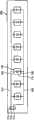
如图11中所示,根据一个实施例的包括发光二极管封装件的背光单元(在下文中,称作背光单元)包括基体构件200、安装在基体构件200上的多个发光二极管封装件100以及将从外部施加的驱动电压提供至发光二极管封装件100的信号线。As shown in FIG. 11 , a backlight unit including a light emitting diode package (hereinafter, referred to as a backlight unit) according to one embodiment includes a
发光二极管封装件100产生光。由于发光二极管封装件100可以包括参照图1至图10描述的发光二极管中的一种,所以将省略发光二极管封装件100的详述。The light emitting
基体构件200包括形成背光单元的框架的板构件,并且可以包括树脂基底或其表面上形成有金属氧化物层的金属基底(例如,其上设置有铝氧化物层(或氧化铝层)的铝基底)。The
如图11中所示,发光二极管封装件100可以彼此并联连接。信号线包括第一信号线310和第二信号线320,第一信号线310将第一电压提供至每个发光二极管封装件100的第一主引线120,第二信号线320将比第一电压低的第二电压提供至每个发光二极管封装件100的第二主引线130。信号线包括诸如铜(Cu)的导电材料,并可以通过镀覆工艺或蚀刻工艺形成。As shown in FIG. 11 , the light emitting
当基体构件200包括连接件210时,第一信号线连接到第一引脚212以从外部接收适于驱动发光二极管110的较高的电压,第二信号线连接到第二引脚214以从外部接收接地电压。When the
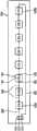
如图12中所示,发光二极管封装件100可以彼此串联连接。在这种情况下,发光二极管封装件100串联地布置,信号线包括第三信号线330和多个第四信号线340,第三信号线330将第一电压提供至发光二极管封装件100A的第一主引线120,发光二极管封装件100A是发光二极管封装件100中布置在最前面的发光二极管封装件,多个第四信号线340将设置在相邻的发光二极管封装件100之间的第一主引线120和第二主引线130连接。此外,信号线包括第五信号线350,以将比第一电压低的第二电压提供至发光二极管封装件100N的第二主引线130,发光二极管封装件100N是发光二极管封装件100中布置在最后的发光二极管封装件。As shown in FIG. 12, the light emitting
图13是示出根据本发明又一实施例的背光单元的侧视图。除图11或图12中的背光单元的结构之外,图13中的背光单元还包括导光板400。FIG. 13 is a side view showing a backlight unit according to still another embodiment of the present invention. The backlight unit in FIG. 13 further includes a
导光板400通过至少一个侧表面410接收从发光二极管封装件100入射的光,以通过光出射表面420输出所述光。The
导光板400可以具有矩形板的形状。在这种情况下,导光板400包括与发光二极管封装件100相邻的侧表面410、从侧表面410的一端延伸的光出射表面420以及与光出射表面420平行地从侧表面410的相对端延伸的反射表面430。The
从发光二极管封装件100输出的光入射到导光板400的侧表面410上。通过侧表面410入射到导光板400内部的光通过光出射表面420输出到外部,或者在所述光被反射表面430反射后通过光出射表面420输出。Light output from the light emitting
为了提高入射到导光板400中的光的收集效率,每个发光二极管封装件100的发光表面100L优选地平行于导光板400的侧表面410。In order to improve collection efficiency of light incident into the
此外,背光单元还可以包括设置在光出射表面420上方的漫射片500和面对漫射片500的反射片600,同时导光板400设置在漫射片500与反射片600之间。反射片600将从导光板400泄漏的光向导光板400再次反射,漫射片500使从导光板400输出的光漫射。因此,可以提高背光的亮度。In addition, the backlight unit may further include a
虽然图13示出了发光二极管封装件100与导光板400的一个侧表面相邻地设置,但背光单元可以具有发光二极管封装件100与导光板400的至少两个侧表面分别相邻的结构。Although FIG. 13 shows that the LED packages 100 are disposed adjacent to one side surface of the
如上所述,根据本发明的示例性实施例,发光二极管封装件通过第一子引线和第二子引线释放静电,以保护发光二极管不受放电电流的损坏。As described above, according to an exemplary embodiment of the present invention, the light emitting diode package discharges static electricity through the first sub-lead and the second sub-lead to protect the light emitting diode from being damaged by the discharge current.
此外,发光二极管封装件不需要诸如瞬态电压抑制二极管或齐纳二极管的另外的二极管来保护发光二极管。因此,可以降低制造成本,可以简化结构,并且可以提高亮度。Furthermore, the LED package does not require additional diodes such as transient voltage suppressor diodes or Zener diodes to protect the LEDs. Therefore, the manufacturing cost can be reduced, the structure can be simplified, and the luminance can be improved.
包括发光二极管封装件的背光单元可以表现出低功耗和提高的亮度。A backlight unit including light emitting diode packages may exhibit low power consumption and improved brightness.
虽然已描述了本发明的示例性实施例,但应该理解的是,本发明不应该局限于这些示例性实施例,而是在由权利要求限定的本发明的精神和范围内,本领域普通技术人员可以做出各种改变和修改。对本领域技术人员明显的将是,在不脱离本发明的精神或范围的情况下,可以对本发明做出各种修改和改变。因此,只要对本发明的修改和改变落入权利要求书及其等同物的范围内,本发明就意图覆盖这些修改和改变。Although exemplary embodiments of the present invention have been described, it should be understood that the present invention should not be limited to these exemplary embodiments, but within the spirit and scope of the present invention defined by the claims, those skilled in the art Personnel may make various changes and modifications. It will be apparent to those skilled in the art that various modifications and changes can be made in the present invention without departing from the spirit or scope of the inventions. Therefore, it is intended that the present invention cover the modifications and changes of this invention provided they come within the scope of the claims and their equivalents.
Claims (10)
Applications Claiming Priority (2)
| Application Number | Priority Date | Filing Date | Title |
|---|---|---|---|
| KR10-2011-0012008 | 2011-02-10 | ||
| KR1020110012008AKR101783955B1 (en) | 2011-02-10 | 2011-02-10 | Light emitting diode package and back light unit having the same |
Publications (2)
| Publication Number | Publication Date |
|---|---|
| CN102637676Atrue CN102637676A (en) | 2012-08-15 |
| CN102637676B CN102637676B (en) | 2016-06-15 |
Family
ID=46622018
Family Applications (1)
| Application Number | Title | Priority Date | Filing Date |
|---|---|---|---|
| CN201210025015.4AExpired - Fee RelatedCN102637676B (en) | 2011-02-10 | 2012-02-01 | Light emission diode package member and there is the back light unit of this light emission diode package member |
Country Status (4)
| Country | Link |
|---|---|
| US (1) | US8801256B2 (en) |
| JP (1) | JP5955013B2 (en) |
| KR (1) | KR101783955B1 (en) |
| CN (1) | CN102637676B (en) |
Cited By (1)
| Publication number | Priority date | Publication date | Assignee | Title |
|---|---|---|---|---|
| CN110429080A (en)* | 2019-08-12 | 2019-11-08 | 厦门多彩光电子科技有限公司 | A kind of packaging method and Mini LED of Mini LED |
Families Citing this family (7)
| Publication number | Priority date | Publication date | Assignee | Title |
|---|---|---|---|---|
| JP5869961B2 (en)* | 2012-05-28 | 2016-02-24 | 株式会社東芝 | Semiconductor light emitting device |
| JP6205894B2 (en)* | 2012-07-04 | 2017-10-04 | 日亜化学工業株式会社 | Package molded body for light emitting device and light emitting device using the same |
| CN102878495B (en)* | 2012-10-12 | 2016-05-25 | 北京京东方光电科技有限公司 | The preparation method of backlight, backlight and display unit |
| GB201420860D0 (en)* | 2014-11-24 | 2015-01-07 | Infiniled Ltd | Micro-LED device |
| JP6617452B2 (en)* | 2015-07-07 | 2019-12-11 | 日亜化学工業株式会社 | Linear light source |
| KR20180032206A (en)* | 2016-09-21 | 2018-03-29 | 포산 내션스타 옵토일렉트로닉스 코., 엘티디 | LED support, LED elements and LED screen |
| US11961872B2 (en)* | 2020-04-29 | 2024-04-16 | Seoul Viosys Co., Ltd. | Unit pixel having light emitting devices and display apparatus having the same |
Citations (7)
| Publication number | Priority date | Publication date | Assignee | Title |
|---|---|---|---|---|
| CN1619845A (en)* | 2003-11-18 | 2005-05-25 | Itswell株式会社 | Semiconductor light emitting diode and manufacturing method thereof |
| CN1661823A (en)* | 2004-02-23 | 2005-08-31 | 斯坦雷电气株式会社 | LED and its manufacturing method |
| CN2739804Y (en)* | 2004-03-04 | 2005-11-09 | 星衍股份有限公司 | Light-emitting diode anti-static device |
| CN1707823A (en)* | 2004-06-10 | 2005-12-14 | Lg电子有限公司 | High Power LED Packaging |
| CN101030572A (en)* | 2006-03-01 | 2007-09-05 | 瑞莹光电股份有限公司 | Light emitting diode package and manufacturing method thereof |
| US20090085458A1 (en)* | 2003-10-28 | 2009-04-02 | Nichia Corporation | Fluorescent material and light-emitting device |
| WO2010071386A2 (en)* | 2008-12-19 | 2010-06-24 | 삼성엘이디 주식회사 | Light emitting device package, backlight unit, display device and lighting device |
Family Cites Families (15)
| Publication number | Priority date | Publication date | Assignee | Title |
|---|---|---|---|---|
| JPH0951149A (en)* | 1995-08-07 | 1997-02-18 | Canon Inc | Printed wiring board and method of manufacturing the same |
| EP2116816B1 (en)* | 2002-09-20 | 2013-05-01 | Yazaki Corporation | Movement module and meter employing the same |
| KR100593934B1 (en) | 2005-03-23 | 2006-06-30 | 삼성전기주식회사 | LED Package with Electrostatic Discharge Protection |
| US7940155B2 (en)* | 2005-04-01 | 2011-05-10 | Panasonic Corporation | Varistor and electronic component module using same |
| KR101232505B1 (en)* | 2005-06-30 | 2013-02-12 | 엘지디스플레이 주식회사 | Method of fabrication light emission diode package and backlight unit and liquid crystal display device |
| KR100638876B1 (en)* | 2005-07-22 | 2006-10-27 | 삼성전기주식회사 | Side type light emitting diode with improved arrangement of protection elements |
| KR20070111091A (en) | 2006-05-16 | 2007-11-21 | 삼성전기주식회사 | Nitride-based Semiconductor Light-Emitting Diodes |
| TW200802928A (en)* | 2006-06-13 | 2008-01-01 | Bright View Electronics Co Ltd | A flexible ribbon illumination device and manufacture method thereof |
| KR101294008B1 (en)* | 2006-07-24 | 2013-08-07 | 삼성디스플레이 주식회사 | Backlight assembly, method of manufacturing the same and display device having the same |
| KR101320021B1 (en)* | 2006-10-17 | 2013-10-18 | 삼성디스플레이 주식회사 | Light source, backlight assembly and liquid crystal display having the same |
| KR100896068B1 (en) | 2007-11-30 | 2009-05-07 | 일진반도체 주식회사 | Light Emitting Diode Device with Electrostatic Discharge Protection |
| JP2010087071A (en)* | 2008-09-30 | 2010-04-15 | Hitachi Automotive Systems Ltd | Electric circuit |
| JP5660699B2 (en)* | 2009-06-16 | 2015-01-28 | パナソニックIpマネジメント株式会社 | LED light emitting device, LED module, and lighting device |
| WO2012050110A1 (en)* | 2010-10-12 | 2012-04-19 | ローム株式会社 | Led module |
| KR20130022060A (en)* | 2011-08-24 | 2013-03-06 | 삼성디스플레이 주식회사 | Backlight assembly and method of manufacturing the same |
- 2011
- 2011-02-10KRKR1020110012008Apatent/KR101783955B1/ennot_activeExpired - Fee Related
- 2011-12-27USUS13/337,722patent/US8801256B2/enactiveActive
- 2012
- 2012-02-01CNCN201210025015.4Apatent/CN102637676B/ennot_activeExpired - Fee Related
- 2012-02-10JPJP2012027773Apatent/JP5955013B2/ennot_activeExpired - Fee Related
Patent Citations (7)
| Publication number | Priority date | Publication date | Assignee | Title |
|---|---|---|---|---|
| US20090085458A1 (en)* | 2003-10-28 | 2009-04-02 | Nichia Corporation | Fluorescent material and light-emitting device |
| CN1619845A (en)* | 2003-11-18 | 2005-05-25 | Itswell株式会社 | Semiconductor light emitting diode and manufacturing method thereof |
| CN1661823A (en)* | 2004-02-23 | 2005-08-31 | 斯坦雷电气株式会社 | LED and its manufacturing method |
| CN2739804Y (en)* | 2004-03-04 | 2005-11-09 | 星衍股份有限公司 | Light-emitting diode anti-static device |
| CN1707823A (en)* | 2004-06-10 | 2005-12-14 | Lg电子有限公司 | High Power LED Packaging |
| CN101030572A (en)* | 2006-03-01 | 2007-09-05 | 瑞莹光电股份有限公司 | Light emitting diode package and manufacturing method thereof |
| WO2010071386A2 (en)* | 2008-12-19 | 2010-06-24 | 삼성엘이디 주식회사 | Light emitting device package, backlight unit, display device and lighting device |
Cited By (1)
| Publication number | Priority date | Publication date | Assignee | Title |
|---|---|---|---|---|
| CN110429080A (en)* | 2019-08-12 | 2019-11-08 | 厦门多彩光电子科技有限公司 | A kind of packaging method and Mini LED of Mini LED |
Also Published As
| Publication number | Publication date |
|---|---|
| JP2012169624A (en) | 2012-09-06 |
| US8801256B2 (en) | 2014-08-12 |
| CN102637676B (en) | 2016-06-15 |
| KR20120091905A (en) | 2012-08-20 |
| JP5955013B2 (en) | 2016-07-20 |
| KR101783955B1 (en) | 2017-10-11 |
| US20120206934A1 (en) | 2012-08-16 |
Similar Documents
| Publication | Publication Date | Title |
|---|---|---|
| CN102637676B (en) | Light emission diode package member and there is the back light unit of this light emission diode package member | |
| JP6283483B2 (en) | LIGHT EMITTING ELEMENT AND LIGHTING SYSTEM HAVING THE SAME | |
| CN102903837B (en) | Light emitting device packaging piece and include its illuminator | |
| CN106876376B (en) | Light emitting device packaging piece and light unit including it | |
| US8395182B2 (en) | Light emitting device, light emitting device package, method of manufacturing light emitting device and illumination system | |
| CN103066172B (en) | Light emitting device | |
| CN102194932B (en) | Light emitting diode and fabrication method thereof | |
| CN103682068B (en) | Light-emitting device | |
| CN102956779B (en) | Luminescent device and light emitting device packaging piece | |
| JP2014057062A (en) | Light emitting element and lighting system having the same | |
| CN102966880A (en) | Light emitting module and backlight unit having the same | |
| CN105453280B (en) | Luminescent device | |
| KR102075561B1 (en) | Light emitting device, lightr emitting module and lighting system | |
| CN102651439B (en) | Luminescent device and illuminator | |
| US10270006B2 (en) | Light emitting device and light emitting module | |
| CN103579430B (en) | Luminescent device | |
| KR101916148B1 (en) | Light emitting device, manufactured method of the light emitting device and lighting system | |
| KR101926507B1 (en) | Light emitting device, method for fabricating the same, and light emitting device package | |
| KR101873585B1 (en) | Light emitting device package and lighting system having the same | |
| CN102623585B (en) | Luminescent device | |
| KR102053279B1 (en) | Light emitting device, light emitting device package, and light unit | |
| KR102019498B1 (en) | Light emitting device and lighting system | |
| KR101946831B1 (en) | Light emitting device package | |
| US20110291150A1 (en) | Led illumination device | |
| CN102447032B (en) | Luminescent device |
Legal Events
| Date | Code | Title | Description |
|---|---|---|---|
| C06 | Publication | ||
| PB01 | Publication | ||
| ASS | Succession or assignment of patent right | Owner name:SAMSUNG DISPLAY CO., LTD. Free format text:FORMER OWNER: SAMSUNG ELECTRONICS CO., LTD. Effective date:20121219 | |
| C41 | Transfer of patent application or patent right or utility model | ||
| TA01 | Transfer of patent application right | Effective date of registration:20121219 Address after:South Korea Gyeonggi Do Yongin Applicant after:Samsung Display Co.,Ltd. Address before:Gyeonggi Do Korea Suwon Applicant before:Samsung Electronics Co.,Ltd. | |
| C10 | Entry into substantive examination | ||
| SE01 | Entry into force of request for substantive examination | ||
| C14 | Grant of patent or utility model | ||
| GR01 | Patent grant | ||
| CF01 | Termination of patent right due to non-payment of annual fee | Granted publication date:20160615 Termination date:20210201 | |
| CF01 | Termination of patent right due to non-payment of annual fee |