CN102637602A - Method for reducing grid-induction drain leakage of semiconductor device - Google Patents
Method for reducing grid-induction drain leakage of semiconductor deviceDownload PDFInfo
- Publication number
- CN102637602A CN102637602ACN2012100473843ACN201210047384ACN102637602ACN 102637602 ACN102637602 ACN 102637602ACN 2012100473843 ACN2012100473843 ACN 2012100473843ACN 201210047384 ACN201210047384 ACN 201210047384ACN 102637602 ACN102637602 ACN 102637602A
- Authority
- CN
- China
- Prior art keywords
- semiconductor device
- drain
- etching
- side wall
- grid
- Prior art date
- Legal status (The legal status is an assumption and is not a legal conclusion. Google has not performed a legal analysis and makes no representation as to the accuracy of the status listed.)
- Pending
Links
- 238000000034methodMethods0.000titleclaimsabstractdescription33
- 239000004065semiconductorSubstances0.000titleclaimsabstractdescription25
- 238000005530etchingMethods0.000claimsabstractdescription21
- 239000000758substrateSubstances0.000claimsabstractdescription11
- 238000000137annealingMethods0.000claimsabstractdescription4
- VYPSYNLAJGMNEJ-UHFFFAOYSA-NSilicium dioxideChemical groupO=[Si]=OVYPSYNLAJGMNEJ-UHFFFAOYSA-N0.000claimsdescription4
- 229910052581Si3N4Inorganic materials0.000claimsdescription3
- 238000001312dry etchingMethods0.000claimsdescription3
- HQVNEWCFYHHQES-UHFFFAOYSA-Nsilicon nitrideChemical compoundN12[Si]34N5[Si]62N3[Si]51N64HQVNEWCFYHHQES-UHFFFAOYSA-N0.000claimsdescription3
- 238000011982device technologyMethods0.000claims1
- 238000000926separation methodMethods0.000claims1
- 239000000377silicon dioxideSubstances0.000claims1
- 230000005684electric fieldEffects0.000abstractdescription6
- 238000002955isolationMethods0.000abstractdescription3
- 150000002500ionsChemical class0.000description13
- 239000002019doping agentSubstances0.000description7
- 238000010586diagramMethods0.000description4
- 230000005641tunnelingEffects0.000description4
- 239000000969carrierSubstances0.000description3
- 230000000694effectsEffects0.000description3
- 125000006850spacer groupChemical group0.000description3
- 238000004519manufacturing processMethods0.000description2
- 238000012986modificationMethods0.000description2
- 230000004048modificationEffects0.000description2
- 229910052814silicon oxideInorganic materials0.000description2
- 230000009286beneficial effectEffects0.000description1
- 230000007423decreaseEffects0.000description1
- 230000008021depositionEffects0.000description1
- 238000009826distributionMethods0.000description1
- 238000002360preparation methodMethods0.000description1
- 238000006467substitution reactionMethods0.000description1
Images


Classifications
- H—ELECTRICITY
- H10—SEMICONDUCTOR DEVICES; ELECTRIC SOLID-STATE DEVICES NOT OTHERWISE PROVIDED FOR
- H10D—INORGANIC ELECTRIC SEMICONDUCTOR DEVICES
- H10D30/00—Field-effect transistors [FET]
- H10D30/01—Manufacture or treatment
- H10D30/021—Manufacture or treatment of FETs having insulated gates [IGFET]
- H10D30/0221—Manufacture or treatment of FETs having insulated gates [IGFET] having asymmetry in the channel direction, e.g. lateral high-voltage MISFETs having drain offset region or extended-drain MOSFETs [EDMOS]
- H—ELECTRICITY
- H10—SEMICONDUCTOR DEVICES; ELECTRIC SOLID-STATE DEVICES NOT OTHERWISE PROVIDED FOR
- H10D—INORGANIC ELECTRIC SEMICONDUCTOR DEVICES
- H10D30/00—Field-effect transistors [FET]
- H10D30/60—Insulated-gate field-effect transistors [IGFET]
- H10D30/601—Insulated-gate field-effect transistors [IGFET] having lightly-doped drain or source extensions, e.g. LDD IGFETs or DDD IGFETs
- H10D30/603—Insulated-gate field-effect transistors [IGFET] having lightly-doped drain or source extensions, e.g. LDD IGFETs or DDD IGFETs having asymmetry in the channel direction, e.g. lateral high-voltage MISFETs having drain offset region or extended drain IGFETs [EDMOS]
Landscapes
- Insulated Gate Type Field-Effect Transistor (AREA)
- Semiconductor Memories (AREA)
Abstract
Description
Translated fromChinese技术领域technical field
本发明涉及半导体制备技术领域,尤其涉及一种减小半导体器件栅诱导漏极泄漏的方法。The invention relates to the technical field of semiconductor preparation, in particular to a method for reducing gate-induced drain leakage of semiconductor devices.
背景技术Background technique
栅致漏极泄漏(GIDL,Gate-Induced Drain Leakage)是指,当器件在关断(off-state)的情况下(即Vg=0),若漏极与Vdd相连(即Vd=Vdd),由于栅极和漏极之间的交叠,在栅极和漏极之间的交叠区域会存在强电场,载流子会在强电场作用下发生带带隧穿效应(Band-to-band Tunneling),从而引起漏极到栅极之间的漏电流。Gate-Induced Drain Leakage (GIDL, Gate-Induced Drain Leakage) means that when the device is off-state (ie Vg=0), if the drain is connected to Vdd (ie Vd=Vdd), Due to the overlap between the gate and the drain, there will be a strong electric field in the overlapping region between the gate and the drain, and the carriers will undergo band-to-band tunneling under the action of the strong electric field. Tunneling), causing leakage current from drain to gate.
栅致漏极泄漏电流已经成为影响小尺寸MOS器件可靠性、功耗等方面的主要原因之一,它同时也对EEPROM等存储器件的擦写操作有重要影响。当工艺进入超深亚微米时代后,由于器件尺寸日益缩小,GIDL电流引发的众多可靠性问题变得愈加严重。The gate-induced-drain leakage current has become one of the main reasons affecting the reliability and power consumption of small-sized MOS devices, and it also has an important impact on the erasing and writing operations of memory devices such as EEPROM. When the process enters the ultra-deep submicron era, due to the shrinking device size, many reliability problems caused by GIDL current become more and more serious.
中国专利CN 101350301A公开了一种半导体器件及其制造方法,该制造方法可以包括:在半导体衬底上选择性地形成氧化层图样,在相同的衬底上形成绝缘层图样以覆盖该氧化层图样的边缘部分,蚀刻该氧化层图样和该衬底以形成凹槽和相应于该氧化层图样边缘部分的第一和第二氧化层图样,在凹槽中的衬底上形成第三氧化层图样以产生包括第一、第二和第三氧化层图样的栅极绝缘层,以及在该凹槽中形成栅极图样。该方法工艺较为复杂。Chinese patent CN 101350301A discloses a semiconductor device and its manufacturing method, which may include: selectively forming an oxide layer pattern on a semiconductor substrate, and forming an insulating layer pattern on the same substrate to cover the oxide layer pattern The edge portion of the oxide layer pattern and the substrate are etched to form a groove and the first and second oxide layer patterns corresponding to the edge portion of the oxide layer pattern, and a third oxide layer pattern is formed on the substrate in the groove to generate a gate insulating layer including the first, second and third oxide layer patterns, and form a gate pattern in the groove. The process of this method is relatively complicated.
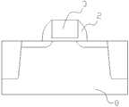
通常工艺中,侧墙刻蚀工艺如图1A~1C所示,首先是在具有栅极3的衬底0表面进行侧墙薄膜1沉积,沉积后器件的截面如图1A所示;接下来采用各向异性的干法刻蚀,刻蚀后源漏极上方的侧墙2成对称结构,如图1B所示;然后是源漏重掺杂以及退火工艺,源漏形成的掺杂离子分布如图1C所示,掺杂离子距离器件沟道的距离,由侧墙2的宽度所决定。In the usual process, the sidewall etching process is shown in Figures 1A to 1C. First, the
发明内容Contents of the invention
针对上述存在的问题,本发明的目的是提供一种减小半导体器件栅诱导漏极泄漏的方法,在保持沟道有效长度(Effective Channel Length)不变的情况下,降低了漏端的纵向电场强度,从而减小了半导体器件栅致漏极泄漏电流,工艺简单。In view of the above existing problems, the object of the present invention is to provide a method for reducing gate-induced drain leakage of semiconductor devices, which reduces the vertical electric field intensity at the drain end while keeping the effective channel length (Effective Channel Length) constant. , thereby reducing the gate-induced-drain leakage current of the semiconductor device, and the process is simple.
本发明的目的是通过下述技术方案实现的:The purpose of the present invention is achieved through the following technical solutions:
一种减小半导体器件栅诱导漏极泄漏的方法,其中,包括下列步骤:A method for reducing gate-induced drain leakage of a semiconductor device, comprising the following steps:
在一已完成两侧浅沟槽隔离工艺的衬底上生长一层侧墙薄膜;growing a layer of sidewall film on a substrate that has completed the shallow trench isolation process on both sides;
对侧墙薄膜进行刻蚀,引入的刻蚀等离子体从朝向于源极的入射点进行并与竖直方向形成一定角度,在半导体器件的栅极上形成侧墙,并使得刻蚀后的侧墙源极的宽度减小,漏极的宽度增大;Etching the side wall film, the introduced etching plasma is carried out from the incident point towards the source and forms a certain angle with the vertical direction, forming a side wall on the gate of the semiconductor device, and making the etched side wall The width of the wall source decreases and the width of the drain increases;
进行源漏重掺杂以及退火工艺。Perform source and drain heavy doping and annealing processes.
在本发明的又一个实施例中,在45nm CMOS器件工艺中,引入的刻蚀等离子体入射方向与竖直方向成15度。In yet another embodiment of the present invention, in the 45nm CMOS device process, the incident direction of the introduced etching plasma is 15 degrees from the vertical direction.
在本发明的另一个实施例中,在衬底源极与栅极的交界处、以及漏极与栅极的交界处分别具有低掺杂源漏区。In another embodiment of the present invention, there are low-doped source and drain regions at the junction of the source and the gate of the substrate, and at the junction of the drain and the gate, respectively.
在本发明的又一个实施例中,所述侧墙薄膜为氧化硅或者氮化硅薄膜。In yet another embodiment of the present invention, the sidewall film is a silicon oxide or silicon nitride film.
在本发明的另一个实施例中,对侧墙薄膜进行的刻蚀是采用干法刻蚀。In another embodiment of the present invention, the etching of the sidewall film is performed by dry etching.
与已有技术相比,本发明的有益效果在于:Compared with prior art, the beneficial effect of the present invention is:
1、不增加现有的MOS器件制造工艺步骤。1. The existing MOS device manufacturing process steps are not added.
2、通过斜角侧墙刻蚀工艺,增加了刻蚀后漏端的侧墙宽度,减小了刻蚀后源端得侧墙宽度。2. Through the bevel sidewall etching process, the sidewall width of the drain end after etching is increased, and the sidewall width of the source end after etching is reduced.
3、在漏端,由于重掺杂离子与沟道间的距离被拉远,当栅极关断而漏极接Vdd时,在栅极与漏端交叠区域的电场强度减弱,从而降低了载流子的带带隧穿效应,减小了半导体器件栅致漏极泄漏电流。3. At the drain end, since the distance between the heavily doped ions and the channel is pulled away, when the gate is turned off and the drain is connected to Vdd, the electric field strength in the overlapping area of the gate and drain ends is weakened, thereby reducing the The band-band tunneling effect of carriers reduces the gate-induced-drain leakage current of semiconductor devices.
4、在漏端的掺杂离子与沟道的距离被拉远的同时,源端的掺杂离子与沟道的距离被拉近,因此器件的有效沟道长度基本保持不变,器件的其他性能得以保持。4. While the distance between the dopant ions at the drain end and the channel is shortened, the distance between the dopant ions at the source end and the channel is shortened, so the effective channel length of the device remains basically unchanged, and other performances of the device can be improved. Keep.
附图说明Description of drawings
图1A、图1B和图1C是传统工艺的侧墙刻蚀工艺步骤示意图;FIG. 1A, FIG. 1B and FIG. 1C are schematic diagrams of sidewall etching process steps in a conventional process;
图2是本发明减小半导体器件栅诱导漏极泄露的方法的流程示意图;2 is a schematic flow chart of a method for reducing gate-induced drain leakage of a semiconductor device according to the present invention;
图3A、图3B和图3C是本发明减小半导体器件栅诱导漏极泄漏的方法步骤示意图。Fig. 3A, Fig. 3B and Fig. 3C are schematic diagrams of the steps of the method for reducing gate-induced drain leakage of a semiconductor device according to the present invention.
具体实施方式Detailed ways
下面结合原理图和具体操作实施例对本发明作进一步说明。The present invention will be further described below in combination with principle diagrams and specific operation examples.
参看图2所示,本发明减小半导体器件栅诱导漏极泄漏的方法具体包括下列步骤:Referring to Figure 2, the method for reducing the gate-induced drain leakage of a semiconductor device in the present invention specifically includes the following steps:
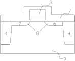
如图3A所示,在一已完成两侧浅沟槽隔离工艺(STI)4的衬底0上生长一层侧墙薄膜1,侧墙薄膜1可以为氧化硅或者氮化硅薄膜,在衬底源极与栅极的交界处、以及漏极与栅极的交界处分别具有低掺杂源漏区(LDD)8。对侧墙薄膜1进行干法刻蚀,具体地,对侧墙薄膜1进行的是采用具有各向异性的等离子体干法刻蚀,引入的刻蚀等离子体5从朝向于源极7的入射点进行并与竖直方向形成一定角度α,在半导体器件的栅极3上形成侧墙2,并使得刻蚀后的侧墙2源极的宽度减小,漏极的宽度增大,完成后的效果图如图3B所示。在本发明的一个具体实施例中,在45nm CMOS器件工艺中,引入的刻蚀等离子体5入射方向与竖直方向成15度。As shown in FIG. 3A, a layer of
刻蚀后的侧墙源极6的宽度减小,漏极7的宽度增大,最后进行源漏重掺杂以及退火工艺,最终完成后的半导体截面图如图3C所示。由于掺杂离子与器件沟道的距离由侧墙2的宽度所决定,因此掺杂后,源端的掺杂离子与器件沟道的距离被拉近,漏极7的掺杂离子与器件沟道的距离被拉远,但由于源漏侧墙的宽度之和保持不变,所以源漏重掺杂离子之间的距离保持不变。After etching, the width of the
在漏极7,由于重掺杂离子与沟道间的距离被拉远,当栅极3关断而漏极7接Vdd时,在栅极3与漏极7交叠区域的电场强度减弱,从而降低了载流子的带带隧穿效应,减小了半导体器件栅致漏极泄漏电流。此外,由于在漏极7的重掺杂离子与沟道的距离被拉远的同时,源极6的重掺杂离子与沟道的距离被拉近,总的源漏重掺杂离子之间的距离保持不变,因此器件的有效沟道长度基本保持不变,器件的其他性能得以保持,工艺简单。At the
以上对本发明的具体实施例进行了详细描述,但本发明并不限制于以上描述的具体实施例,其只是作为范例。对于本领域技术人员而言,任何等同修改和替代也都在本发明的范畴之中。因此,在不脱离本发明的精神和范围下所作出的均等变换和修改,都应涵盖在本发明的范围内。The specific embodiments of the present invention have been described in detail above, but the present invention is not limited to the specific embodiments described above, which are only examples. For those skilled in the art, any equivalent modifications and substitutions also fall within the scope of the present invention. Therefore, all equivalent changes and modifications made without departing from the spirit and scope of the present invention shall fall within the scope of the present invention.
Claims (5)
Priority Applications (1)
| Application Number | Priority Date | Filing Date | Title |
|---|---|---|---|
| CN2012100473843ACN102637602A (en) | 2012-02-28 | 2012-02-28 | Method for reducing grid-induction drain leakage of semiconductor device |
Applications Claiming Priority (1)
| Application Number | Priority Date | Filing Date | Title |
|---|---|---|---|
| CN2012100473843ACN102637602A (en) | 2012-02-28 | 2012-02-28 | Method for reducing grid-induction drain leakage of semiconductor device |
Publications (1)
| Publication Number | Publication Date |
|---|---|
| CN102637602Atrue CN102637602A (en) | 2012-08-15 |
Family
ID=46621956
Family Applications (1)
| Application Number | Title | Priority Date | Filing Date |
|---|---|---|---|
| CN2012100473843APendingCN102637602A (en) | 2012-02-28 | 2012-02-28 | Method for reducing grid-induction drain leakage of semiconductor device |
Country Status (1)
| Country | Link |
|---|---|
| CN (1) | CN102637602A (en) |
Citations (4)
| Publication number | Priority date | Publication date | Assignee | Title |
|---|---|---|---|---|
| JPH04186732A (en)* | 1990-11-21 | 1992-07-03 | Hitachi Ltd | Semiconductor device and manufacture thereof |
| US20080233691A1 (en)* | 2007-03-23 | 2008-09-25 | Kangguo Cheng | Method of forming asymmetric spacers and methods of fabricating semiconductor device using asymmetric spacers |
| CN101647108A (en)* | 2005-10-07 | 2010-02-10 | 国际商业机器公司 | Structure and method for forming asymmetrical overlap capacitance in field effect transistors |
| CN102437057A (en)* | 2011-08-17 | 2012-05-02 | 上海华力微电子有限公司 | Method for reducing semiconductor device hot carrier injection damage |
- 2012
- 2012-02-28CNCN2012100473843Apatent/CN102637602A/enactivePending
Patent Citations (4)
| Publication number | Priority date | Publication date | Assignee | Title |
|---|---|---|---|---|
| JPH04186732A (en)* | 1990-11-21 | 1992-07-03 | Hitachi Ltd | Semiconductor device and manufacture thereof |
| CN101647108A (en)* | 2005-10-07 | 2010-02-10 | 国际商业机器公司 | Structure and method for forming asymmetrical overlap capacitance in field effect transistors |
| US20080233691A1 (en)* | 2007-03-23 | 2008-09-25 | Kangguo Cheng | Method of forming asymmetric spacers and methods of fabricating semiconductor device using asymmetric spacers |
| CN102437057A (en)* | 2011-08-17 | 2012-05-02 | 上海华力微电子有限公司 | Method for reducing semiconductor device hot carrier injection damage |
Similar Documents
| Publication | Publication Date | Title |
|---|---|---|
| CN107958873A (en) | Fin field effect pipe and forming method thereof | |
| CN102956502B (en) | Method for manufacturing a recessed channel access transistor device | |
| CN104201198A (en) | Tunneling transistor structure and manufacturing method thereof | |
| CN116825818A (en) | Grid full-cladding nanowire field effect transistor device | |
| US20110049625A1 (en) | Asymmetrical transistor device and method of fabrication | |
| CN102364663A (en) | Gate spacer etching method, MOS device manufacturing method and MOS device | |
| US8753945B2 (en) | Method of manufacturing a semiconductor device | |
| CN102931232A (en) | MOS (Metal Oxide Semiconductor) transistor and forming method thereof | |
| US9401425B2 (en) | Semiconductor structure and method for manufacturing the same | |
| CN103377898B (en) | The formation method of semiconductor device, the formation method of fin field effect pipe | |
| CN110718464B (en) | Semiconductor structure and forming method thereof | |
| KR101213723B1 (en) | Semiconductor device and Method for fabricating the same | |
| CN103715087B (en) | Fin formula field effect transistor and manufacture method thereof | |
| KR101140060B1 (en) | semiconductor device and Method for fabricating the same | |
| CN102637602A (en) | Method for reducing grid-induction drain leakage of semiconductor device | |
| CN112652578B (en) | Method of forming semiconductor structure, transistor | |
| CN104282562A (en) | Fin field effect transistor and forming method thereof | |
| CN104465752B (en) | NMOS transistor structure and its manufacture method | |
| CN106024900A (en) | Method for improving gate-induced drain leakage (GIDL), and non-uniform channel doping device | |
| CN102593003B (en) | Method for reducing induction drain electrode leakage of semiconductor device gate | |
| CN102610528B (en) | Method for reducing grid induction drain leakage of semiconductor device and method for manufacturing metal oxide semiconductor (MOS) device | |
| KR101088818B1 (en) | Method of manufacturing semiconductor device | |
| CN104425262B (en) | PMOS transistor structure and its manufacture method | |
| CN102208351B (en) | Preparation method of fence silicon nanowire transistor of air side wall | |
| CN102479715B (en) | Forming method of semiconductor device |
Legal Events
| Date | Code | Title | Description |
|---|---|---|---|
| C06 | Publication | ||
| PB01 | Publication | ||
| C10 | Entry into substantive examination | ||
| SE01 | Entry into force of request for substantive examination | ||
| C02 | Deemed withdrawal of patent application after publication (patent law 2001) | ||
| WD01 | Invention patent application deemed withdrawn after publication | Application publication date:20120815 |