CN102610272A - Programming or erasing method and device of resistive random access memory unit - Google Patents
Programming or erasing method and device of resistive random access memory unitDownload PDFInfo
- Publication number
- CN102610272A CN102610272ACN2011100211085ACN201110021108ACN102610272ACN 102610272 ACN102610272 ACN 102610272ACN 2011100211085 ACN2011100211085 ACN 2011100211085ACN 201110021108 ACN201110021108 ACN 201110021108ACN 102610272 ACN102610272 ACN 102610272A
- Authority
- CN
- China
- Prior art keywords
- memory unit
- resistive
- programming
- resistive memory
- erasing
- Prior art date
- Legal status (The legal status is an assumption and is not a legal conclusion. Google has not performed a legal analysis and makes no representation as to the accuracy of the status listed.)
- Granted
Links
- 238000000034methodMethods0.000titleclaimsabstractdescription29
- 230000015654memoryEffects0.000claimsabstractdescription84
- 238000001514detection methodMethods0.000claimsabstractdescription12
- 238000009826distributionMethods0.000abstractdescription9
- 238000010586diagramMethods0.000description7
- 239000004065semiconductorSubstances0.000description7
- 230000008569processEffects0.000description5
- 238000003860storageMethods0.000description4
- 230000008859changeEffects0.000description3
- 230000009471actionEffects0.000description1
- 238000001994activationMethods0.000description1
- 230000001186cumulative effectEffects0.000description1
- 230000007423decreaseEffects0.000description1
- 238000013461designMethods0.000description1
- 238000011161developmentMethods0.000description1
- 239000007772electrode materialSubstances0.000description1
- 238000005516engineering processMethods0.000description1
- 230000010354integrationEffects0.000description1
- 238000004519manufacturing processMethods0.000description1
- 239000000463materialSubstances0.000description1
- 238000004377microelectronicMethods0.000description1
- 238000012986modificationMethods0.000description1
- 230000004048modificationEffects0.000description1
- 238000012544monitoring processMethods0.000description1
- 230000002093peripheral effectEffects0.000description1
- 230000009466transformationEffects0.000description1
- 230000007704transitionEffects0.000description1
Images


Classifications
- G—PHYSICS
- G11—INFORMATION STORAGE
- G11C—STATIC STORES
- G11C13/00—Digital stores characterised by the use of storage elements not covered by groups G11C11/00, G11C23/00, or G11C25/00
- G11C13/0002—Digital stores characterised by the use of storage elements not covered by groups G11C11/00, G11C23/00, or G11C25/00 using resistive RAM [RRAM] elements
- G11C13/0021—Auxiliary circuits
- G11C13/0069—Writing or programming circuits or methods
- G—PHYSICS
- G11—INFORMATION STORAGE
- G11C—STATIC STORES
- G11C13/00—Digital stores characterised by the use of storage elements not covered by groups G11C11/00, G11C23/00, or G11C25/00
- G11C13/0002—Digital stores characterised by the use of storage elements not covered by groups G11C11/00, G11C23/00, or G11C25/00 using resistive RAM [RRAM] elements
- G11C13/0007—Digital stores characterised by the use of storage elements not covered by groups G11C11/00, G11C23/00, or G11C25/00 using resistive RAM [RRAM] elements comprising metal oxide memory material, e.g. perovskites
- G—PHYSICS
- G11—INFORMATION STORAGE
- G11C—STATIC STORES
- G11C13/00—Digital stores characterised by the use of storage elements not covered by groups G11C11/00, G11C23/00, or G11C25/00
- G11C13/0002—Digital stores characterised by the use of storage elements not covered by groups G11C11/00, G11C23/00, or G11C25/00 using resistive RAM [RRAM] elements
- G11C13/0021—Auxiliary circuits
- G11C13/0069—Writing or programming circuits or methods
- G11C2013/0092—Write characterized by the shape, e.g. form, length, amplitude of the write pulse
Landscapes
- Chemical & Material Sciences (AREA)
- Engineering & Computer Science (AREA)
- Materials Engineering (AREA)
- Semiconductor Memories (AREA)
Abstract
Translated fromChineseDescription
Translated fromChinese技术领域technical field
本发明涉及微电子领域,尤其涉及一种阻变存储器单元的编程或擦除方法及装置。The invention relates to the field of microelectronics, in particular to a method and device for programming or erasing a resistive variable memory unit.
背景技术Background technique
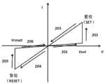
随着现代信息技术的飞速发展,传统的Flash存储器已经不能满足人们对大容量、低功耗存储的需求。阻变存储器单元(RRAM)由于具有结构简单、功耗低、密度高、操作速度快、与CMOS工艺兼容和易于3D集成等优点而受到广泛的关注,是最有前途的下一代非挥发存储器之一。尽管如此,图1所示的阻变存储器单元的阻变参数(如VSet、VReset电压)的离散分布却是其走向实用化的一个瓶颈。为了改善阻变存储器单元阻变参数的离散分布,人们提出了各种各样的解决方法,如选择合适的电极材料、对阻变材料层进行掺杂改性等。With the rapid development of modern information technology, the traditional Flash memory can no longer meet people's demand for large-capacity, low-power storage. Resistive RAM (RRAM), which has attracted extensive attention due to its simple structure, low power consumption, high density, fast operation speed, compatibility with CMOS process, and easy 3D integration, is one of the most promising next-generation non-volatile memories. one. Nevertheless, the discrete distribution of the resistive variable parameters (such as VSet and VReset voltages) of the resistive variable memory cell shown in FIG. 1 is a bottleneck for its practical application. In order to improve the discrete distribution of the resistive switching parameters of the resistive variable memory cell, various solutions have been proposed, such as selecting a suitable electrode material, doping and modifying the resistive variable material layer, and the like.
图2示出了在理想情况下具有双极转换特性的阻变存储器单元的I-V特性曲线示意图。如图2所示,线201、202、203表示电阻由高阻态转变为低阻态的I-V曲线,当电压从0开始向正方向逐渐增大到VSet时,电流急剧增大,表明存储器电阻由高阻态转变为低阻态,称为置位SET(编程)操作;线204至206表示电阻由低阻态转变为高阻态的I-V曲线,当电压从0开始由负方向逐渐增大到VReset时,电流迅速减小,存储器电阻由低阻态转变为高阻态,称为复位RESET(擦除)操作。由图2可以看出,在外加偏压的作用下,阻变存储器单元的电阻会在高低阻态之间发生转换从而实现“0”和“1”的存储。FIG. 2 shows a schematic diagram of the IV characteristic curve of a resistive memory cell with bipolar switching characteristics under ideal conditions. As shown in Figure 2, the
阻变存储器单元常规的编程(置位)和擦除(复位)操作方法如图3所示:对于一个初始态阻变存储器单元,大多数都处于高阻态(HRS),初始的单元并不具有阻变转换特性,需要加一个与置位电压(VSet)同向且高于VSet的电压来激活其转变特性,这个过程称为激活过程301(Forming)。激活后的单元处于低阻态(LRS)。在操作302中,外加一个幅值度很小(小于VSet和VReset的绝对值)的脉冲,来读取此时单元的存储状态。复位操作303时,外加反向偏压的脉冲,脉冲的高度为VReset,阻变存储器单元由低阻态(LRS)转变为高阻态(HRS),复位操作成功。此后可以进行一个读操作304来验证。置位操作305时,外加正向偏压的脉冲,脉冲的高度为VSet,阻变存储器单元由高阻态(HRS)转变为低阻态(LRS),置位操作成功。此后也可以进行一个读操作306来验证。The conventional programming (setting) and erasing (resetting) operation methods of resistive memory cells are shown in Figure 3: for an initial state resistive memory cell, most of them are in the high resistance state (HRS), and the initial cell is not With resistive switching characteristics, it is necessary to apply a voltage that is in the same direction as the set voltage (VSet) and higher than VSet to activate its transformation characteristics. This process is called the activation process 301 (Forming). The activated cell is in the low resistance state (LRS). In
由于编程电压(VSet)和擦除电压(VReset)是很不稳定的,有着很离散的分布,如图1所示,在上述常规的阻变存储器单元的编程和擦除的操作方法中,编程和擦除时脉冲高度的选择将是一件非常困难的事。电压脉冲高度选择过小时,则达不到有些存储器单元的VSet(或VReset)电压,电阻不会发生从高(低)阻态到低(高)阻态的转变,编程(或擦除)操作失败;当电压脉冲高度选择的过大时,会增加阻变存储器单元外围电路的制造成本,而且特别是在RESET的过程中还会引起RESET同SET过程的竞争-RESET过后器件又从高阻态SET回低阻态,导致阻变存储器单元的不稳定。这些对存储器的编程和擦除操作是非常不利的。因此,改善阻变储存器的阻变参数的离散分布,对其走向实用化是非常重要的。Since the programming voltage (VSet ) and the erasing voltage (VReset ) are very unstable and have very discrete distributions, as shown in Figure 1, in the above-mentioned conventional RRAM cell programming and erasing operation method , the selection of pulse height during programming and erasing will be a very difficult thing. If the voltage pulse height is too small, the VSet (or VReset ) voltage of some memory cells will not be reached, and the resistance will not change from a high (low) resistance state to a low (high) resistance state, programming (or erasing) ) operation failure; when the voltage pulse height is selected too large, it will increase the manufacturing cost of the peripheral circuit of the resistive variable memory unit, and especially in the process of RESET, it will also cause competition between RESET and SET process-after RESET, the device will start from high The resistance state SET returns to a low resistance state, resulting in instability of the resistive memory unit. These are very unfavorable to the programming and erasing operations of the memory. Therefore, it is very important to improve the discrete distribution of the resistive variable parameters of the resistive variable memory for its practical application.
发明内容Contents of the invention
为了解决上述的技术问题,提供了一种阻变存储器单元的编程或擦除方法及装置,其目的在于,改善阻变存储器单元的阻变参数分布。In order to solve the above technical problems, a method and device for programming or erasing a resistive memory cell are provided, the purpose of which is to improve the distribution of resistive parameters of the resistive memory cell.
本发明提供了一种阻变存储器单元的编程或擦除装置,包括阻变存储器单元502和晶体管501,还包括:串联电阻503,信号发生器,电流检测装置和控制装置;The present invention provides a programming or erasing device for a resistive variable memory unit, which includes a resistive
信号发生器,用于向所述阻变存储器单元502输入连续的阶梯式脉冲电压信号;a signal generator, configured to input a continuous stepped pulse voltage signal to the
电流检测装置,用于检测所述串联电阻503上的电流;A current detection device, used to detect the current on the
控制装置,用于判断串联电阻503上电流的检测值是否符合预设条件,在检测值符合预设条件时,控制信号发生器终止信号输出,完成阻变存储器单元的编程或擦除操作;在进行编程操作时,所述预设条件为检测值大于预设值;在进行擦除操作时,所述预设条件为检测值小于预设值。The control device is used to judge whether the detection value of the current on the
在进行编程操作时,所述信号发生器向所述阻变存储器单元502输入正向连续的阶梯式脉冲电压信号;在进行擦除操作时,所述信号发生器向所述阻变存储器单元502输入负向连续的阶梯式脉冲电压信号。When performing a programming operation, the signal generator inputs a forward continuous stepped pulse voltage signal to the
正向连续的阶梯式脉冲电压信号的初始值为0V-3V;负向连续的阶梯式脉冲电压信号的初始值为0V-3V。The initial value of the positive continuous step pulse voltage signal is 0V-3V; the initial value of the negative continuous step pulse voltage signal is 0V-3V.
正向连续的阶梯式脉冲电压信号的最大值为1V-6V;负向连续的阶梯式脉冲电压信号的最大值为1V-6V。The maximum value of the positive continuous step pulse voltage signal is 1V-6V; the maximum value of the negative continuous step pulse voltage signal is 1V-6V.
连续的阶梯式脉冲电压信号的脉冲宽度相同,并以恒定的幅度逐渐增加,该幅度的范围为0.1V-0.5V。The pulse width of the continuous stepped pulse voltage signal is the same, and gradually increases with a constant amplitude, and the range of the amplitude is 0.1V-0.5V.
所述串联电阻503连接在所述阻变存储器单元502的上电极与所述信号发生器之间,所述阻变存储器单元502的下电极连接所述晶体管501的漏极。The
本发明提供了一种阻变存储器单元的编程方法,包括:The invention provides a programming method of a resistive memory unit, comprising:
步骤1,对阻变存储器单元502施加正向连续的阶梯式脉冲电压信号;Step 1, applying a forward continuous stepped pulse voltage signal to the resistive
步骤2,检测串联电阻503上的电流;
步骤3,判断串联电阻503上电流的检测值是否符合预设条件,在检测值符合预设条件时,控制信号发生器终止信号输出,完成阻变存储器单元的编程操作。Step 3, judging whether the detected value of the current on the
串联电阻503连接在阻变存储器单元502的上电极与信号发生器之间,阻变存储器单元502的下电极连接晶体管501的漏极。The
所述预设条件为检测值大于预设值。The preset condition is that the detected value is greater than the preset value.
正向连续的阶梯式脉冲电压信号的初始值为0V-3V;正向连续的阶梯式脉冲电压信号的最大值为1V-6V。The initial value of the forward continuous step pulse voltage signal is 0V-3V; the maximum value of the forward continuous step pulse voltage signal is 1V-6V.
正向连续的阶梯式脉冲电压信号的脉冲宽度相同,并以恒定的幅度逐渐增加,该幅度的范围为0.1V-0.5V。The pulse widths of the forward continuous stepped pulse voltage signals are the same, and gradually increase with a constant amplitude, and the range of the amplitude is 0.1V-0.5V.
本发明提供了一种阻变存储器单元的擦除方法,包括:The invention provides a method for erasing a resistive memory unit, comprising:
步骤10,对阻变存储器单元502施加负向连续的阶梯式脉冲电压信号;
步骤20,检测串联电阻503上的电流;
步骤30,判断串联电阻503上电流的检测值是否符合预设条件,在检测值符合预设条件时,控制信号发生器终止信号输出,完成阻变存储器单元的擦除操作。Step 30, judge whether the detected value of the current on the
串联电阻503连接在阻变存储器单元502的上电极与信号发生器之间,阻变存储器单元502的下电极连接晶体管501的漏极。The
负向连续的阶梯式脉冲电压信号的初始值为0V-3V;负向连续的阶梯式脉冲电压信号的最大值为1V-6V。The initial value of the negative continuous step pulse voltage signal is 0V-3V; the maximum value of the negative continuous step pulse voltage signal is 1V-6V.
负向连续的阶梯式脉冲电压信号的脉冲宽度相同,并以恒定的幅度逐渐增加,该幅度的范围为0.1V-0.5V。The pulse width of the negative continuous step-type pulse voltage signal is the same, and gradually increases with a constant amplitude, and the range of the amplitude is 0.1V-0.5V.
本发明能够显著改善阻变存储器单元的阻变参数的离散分布,并且能提高器件的耐久性endurance,延长其使用寿命,并且本发明的技术方案简单、直观,而且速度较快,具有一定实用性的潜能。The present invention can significantly improve the discrete distribution of the resistive variable parameters of the resistive variable memory unit, and can improve the durability of the device and prolong its service life, and the technical solution of the present invention is simple, intuitive, fast, and has certain practicability potential.
附图说明Description of drawings
图1为阻变存储器单元的编程电压VSet和擦除电压VReset的累积分布的示意图;1 is a schematic diagram of the cumulative distribution of programming voltage VSet and erasing voltage VReset of a resistive memory cell;
图2为在理想情况下具有双极转换特性的阻变存储器单元的I-V特性曲线示意图;2 is a schematic diagram of an I-V characteristic curve of a resistive memory cell having bipolar switching characteristics under ideal conditions;
图3为阻变存储器单元常规的编程和擦除操作方法的示意图;3 is a schematic diagram of a conventional programming and erasing operation method of a resistive memory cell;
图4为本发明中阶梯状的连续编程(或擦除)电压脉冲信号示意图;4 is a schematic diagram of a stepped continuous programming (or erasing) voltage pulse signal in the present invention;
图5为本发明中单个阻变存储器单元的编程和擦除装置示意图;5 is a schematic diagram of a programming and erasing device for a single resistive memory cell in the present invention;
图6为本发明中单个阻变存储器单元的编程(或擦除)操作方法的流程图。FIG. 6 is a flow chart of the programming (or erasing) operation method of a single RRAM cell in the present invention.
具体实施方式Detailed ways
为使本发明的目的、技术方案和优点更加清楚明白,以下结合具体实施例,并参照附图,对本发明进一步详细说明。In order to make the object, technical solution and advantages of the present invention clearer, the present invention will be described in further detail below in conjunction with specific embodiments and with reference to the accompanying drawings.
本发明提供了一种阻变存储器单元的编程和擦除的操作方法,通过在阻变存储单元上施加阶梯式电压脉冲,并实时监测阻变存储器单元上的电流来观测其电阻的转变状态,从而完成阻变单元的编程和擦除操作。这种方法能够显著改善阻变存储器单元阻变参数的离散分布。The invention provides an operation method for programming and erasing a resistive memory unit, by applying a stepped voltage pulse on the resistive memory unit and monitoring the current on the resistive memory unit in real time to observe the transition state of its resistance, Thus, the programming and erasing operations of the resistive switching unit are completed. This method can significantly improve the discrete distribution of the resistive parameter of the resistive memory unit.
如图5所示,本发明提供了单个阻变存储器单元的编程和擦除装置示意图。电阻503和阻变存储器单元502的上电极相连,阻变存储器单元502的下电极和晶体管501的漏极相连,构成了1T1R结构,晶体管起着限流作用。脉冲发生器(PG2)504起着输入信号源的作用,它能够按设计要求输入如图4所示的编程(或擦除)的电压脉冲信号。示波器505用来监测流过串联电阻503的电流,从而实时测量阻变存储器单元502中的电流,并将测得的电流大小输入到半导体参数测试仪506中。半导体参数测试仪506同时起到比较电流和控制脉冲发生器504工作状态的作用,即从示波器505输入进的电流与半导体参数测试仪506中预设定的参考值进行比较,并把比较的结果用来控制脉冲发生器504是否继续输出脉冲信号。图5中,半导体参数测试仪506可以为Keithley 4200,HP 4155A,Agilent 4156C等。As shown in FIG. 5 , the present invention provides a schematic diagram of a programming and erasing device for a single RRAM cell. The
阶梯状的连续脉冲编程电压的初始高度由阻变存储器单元的最小SET操作电压决定,取0V~3V;最大的脉冲幅值由阻变存储器单元的最大SET操作电压决定,取1V~6V;脉冲的宽度相同而脉冲的高度逐渐增加,并且每次增加的幅度相同,取0.1V~0.5V。The initial height of the stepped continuous pulse programming voltage is determined by the minimum SET operating voltage of the resistive memory unit, which is 0V to 3V; the maximum pulse amplitude is determined by the maximum SET operating voltage of the resistive memory unit, which is 1V to 6V; The width of the pulse is the same and the height of the pulse increases gradually, and the amplitude of each increase is the same, which is 0.1V ~ 0.5V.
进一步,所述的阶梯状的连续脉冲擦除电压的初始高度由阻变存储器单元的最小RESET操作电压决定,取0V~3V;最大的脉冲幅值由阻变存储器单元的最大RESET操作电压决定,取1V~6V;脉冲的宽度相同而脉冲的高度逐渐增加,并且每次增加的幅度相同,取0.1V~0.5V。以上所提及的电压都是取绝对值后的电压值。Further, the initial height of the stepped continuous pulse erasing voltage is determined by the minimum RESET operating voltage of the resistive memory unit, which is 0V to 3V; the maximum pulse amplitude is determined by the maximum RESET operating voltage of the resistive memory unit, Take 1V ~ 6V; the width of the pulse is the same and the height of the pulse increases gradually, and the amplitude of each increase is the same, take 0.1V ~ 0.5V. The voltages mentioned above are the voltage values after taking the absolute value.
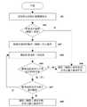
请参照图6,其示出了依照本发明较佳实施例的单个阻变存储器单元的编程(或擦除)操作方法的流程图,具体包括。下面仅以编程操作方法为例来说明其具体的过程:Please refer to FIG. 6 , which shows a flowchart of a programming (or erasing) operation method for a single resistive memory cell according to a preferred embodiment of the present invention, specifically including. The following only takes the programming operation method as an example to illustrate the specific process:
步骤601,对阻变存储器单元进行一个读操作,获取其初始的存储数据状态,来判断该单元是否需要进行编程操作;
步骤602,若该单元初始就处于低阻态,则不需要进行编程操作,直接跳到步骤606;否则,该单元初始就处于高阻态,需要进行编程操作,进入下一步骤603;
步骤603,由脉冲发生器PG2产生如图4所示的阶梯状的连续脉冲电压,脉冲电压的初始高度由阻变存储器单元的最小置位操作电压决定;最大的脉冲幅值由阻变存储器单元的最大置位操作电压决定;脉冲的宽度相同而脉冲的高度逐渐增加,并且每次增加的幅度相同;In
步骤604,测量串联电阻上的电流,通过在示波器上观测串联电阻中电流的变化,来实时监测阻变存储器单元中的电阻变化状态;
步骤605,当在示波器上观测到串联电阻中电流增加时,并且此时的电流值大于半导体参数测试仪中的预设定的参考值时,说明阻变存储器单元由高阻态(HRS)转变为低阻态(LRS),编程操作成功,此时由半导体参数测试仪终止脉冲发生器工作,输入的脉冲信号停止;若串联电阻上的电流值未大于半导体参数测试仪中的预设定的参考值时,说明此时阻变存储器单元仍处在高阻态(HRS),没有发生置位过程,进入步骤607,否则进入步骤606;
步骤606,编程操作成功,停止输入脉冲信号;
步骤607,判断此时输入的脉冲高度是否超过最大脉冲幅度。若没有超过最大脉冲幅度,转到步骤604,直至编程操作成功为止;若超过最大脉冲幅度,进入步骤608;
步骤608,编程操作失败终止脉冲发生器的工作。In
图6中也示出了阻变存储器单元的擦除操作流程,其与阻变存储器单元的编程操作基本类似,这里就不再赘述。FIG. 6 also shows the erasing operation flow of the resistive memory cell, which is basically similar to the programming operation of the resistive memory cell, and will not be repeated here.
本领域的技术人员在不脱离权利要求书确定的本发明的精神和范围的条件下,还可以对以上内容进行各种各样的修改。因此本发明的范围并不仅限于以上的说明,而是由权利要求书的范围来确定的。Various modifications can be made to the above contents by those skilled in the art without departing from the spirit and scope of the present invention defined by the claims. Therefore, the scope of the present invention is not limited to the above description, but is determined by the scope of the claims.
Claims (15)
Translated fromChinesePriority Applications (1)
| Application Number | Priority Date | Filing Date | Title |
|---|---|---|---|
| CN201110021108.5ACN102610272B (en) | 2011-01-19 | 2011-01-19 | Programming and erasing method and device of resistive random access memory unit |
Applications Claiming Priority (1)
| Application Number | Priority Date | Filing Date | Title |
|---|---|---|---|
| CN201110021108.5ACN102610272B (en) | 2011-01-19 | 2011-01-19 | Programming and erasing method and device of resistive random access memory unit |
Publications (2)
| Publication Number | Publication Date |
|---|---|
| CN102610272Atrue CN102610272A (en) | 2012-07-25 |
| CN102610272B CN102610272B (en) | 2015-02-04 |
Family
ID=46527585
Family Applications (1)
| Application Number | Title | Priority Date | Filing Date |
|---|---|---|---|
| CN201110021108.5AActiveCN102610272B (en) | 2011-01-19 | 2011-01-19 | Programming and erasing method and device of resistive random access memory unit |
Country Status (1)
| Country | Link |
|---|---|
| CN (1) | CN102610272B (en) |
Cited By (30)
| Publication number | Priority date | Publication date | Assignee | Title |
|---|---|---|---|---|
| CN103531248A (en)* | 2013-10-12 | 2014-01-22 | 中国科学院微电子研究所 | Method for testing RRAM (resistive random access memory) pulse parameters |
| CN103680602A (en)* | 2012-09-11 | 2014-03-26 | 复旦大学 | Resistive random access memory and reset operation method thereof |
| CN103686822A (en)* | 2012-08-30 | 2014-03-26 | 电信科学技术研究院 | Minimization of drive-tests activation command and result reporting method and equipment |
| CN104464816A (en)* | 2013-09-21 | 2015-03-25 | 庄建祥 | One-time programmable memory, operation method and programming method thereof and electronic system |
| CN104882161A (en)* | 2014-02-28 | 2015-09-02 | 复旦大学 | Resistive random access memory and write operation method thereof |
| CN105304129A (en)* | 2014-07-23 | 2016-02-03 | 华邦电子股份有限公司 | Resistance variable memory and writing method thereof |
| CN106133841A (en)* | 2013-09-21 | 2016-11-16 | 庄建祥 | Single programmable memory body, electronic system, operation single programmable memory body method and programming single programmable memory body method |
| CN106229006A (en)* | 2016-07-07 | 2016-12-14 | 北京兆易创新科技股份有限公司 | A kind of programmed method of memory element |
| CN106257589A (en)* | 2015-06-17 | 2016-12-28 | 旺宏电子股份有限公司 | Variable resistive memory, operating method and operating system thereof |
| CN106816170A (en)* | 2015-11-30 | 2017-06-09 | 华邦电子股份有限公司 | Writing method of resistance type memory cell and resistance type memory |
| US9818478B2 (en) | 2012-12-07 | 2017-11-14 | Attopsemi Technology Co., Ltd | Programmable resistive device and memory using diode as selector |
| CN107636761A (en)* | 2015-06-26 | 2018-01-26 | 英特尔公司 | Magnetic memory cell memory with rebound prevention |
| US9959927B2 (en) | 2016-03-04 | 2018-05-01 | Silicon Storage Technology, Inc. | Multi-step voltage for forming resistive access memory (RRAM) cell filament |
| CN108574485A (en)* | 2017-03-08 | 2018-09-25 | 株式会社东芝 | Integrated circuit with memory and writing method |
| US10127992B2 (en) | 2010-08-20 | 2018-11-13 | Attopsemi Technology Co., Ltd. | Method and structure for reliable electrical fuse programming |
| US10192615B2 (en) | 2011-02-14 | 2019-01-29 | Attopsemi Technology Co., Ltd | One-time programmable devices having a semiconductor fin structure with a divided active region |
| US10229746B2 (en) | 2010-08-20 | 2019-03-12 | Attopsemi Technology Co., Ltd | OTP memory with high data security |
| CN110036444A (en)* | 2016-09-21 | 2019-07-19 | 合肥睿科微电子有限公司 | Adaptive memory cell write conditions |
| US10490297B2 (en) | 2017-06-27 | 2019-11-26 | Winbond Electronics Corp. | Memory storage apparatus and method for testing memory storage apparatus |
| US10535413B2 (en) | 2017-04-14 | 2020-01-14 | Attopsemi Technology Co., Ltd | Low power read operation for programmable resistive memories |
| US10586832B2 (en) | 2011-02-14 | 2020-03-10 | Attopsemi Technology Co., Ltd | One-time programmable devices using gate-all-around structures |
| US10726914B2 (en) | 2017-04-14 | 2020-07-28 | Attopsemi Technology Co. Ltd | Programmable resistive memories with low power read operation and novel sensing scheme |
| CN111564168A (en)* | 2019-02-13 | 2020-08-21 | 旺宏电子股份有限公司 | Control method of progressive resistance characteristic of resistive memory element |
| US10770160B2 (en) | 2017-11-30 | 2020-09-08 | Attopsemi Technology Co., Ltd | Programmable resistive memory formed by bit slices from a standard cell library |
| US10916317B2 (en) | 2010-08-20 | 2021-02-09 | Attopsemi Technology Co., Ltd | Programmable resistance memory on thin film transistor technology |
| US10923204B2 (en) | 2010-08-20 | 2021-02-16 | Attopsemi Technology Co., Ltd | Fully testible OTP memory |
| CN112382331A (en)* | 2020-10-27 | 2021-02-19 | 清华大学 | Method for extracting conductance relaxation effect characteristic parameters of resistive random access memory |
| US11062786B2 (en) | 2017-04-14 | 2021-07-13 | Attopsemi Technology Co., Ltd | One-time programmable memories with low power read operation and novel sensing scheme |
| US11615859B2 (en) | 2017-04-14 | 2023-03-28 | Attopsemi Technology Co., Ltd | One-time programmable memories with ultra-low power read operation and novel sensing scheme |
| CN119562755A (en)* | 2024-10-14 | 2025-03-04 | 清华大学 | Resistive memory processing method, device, electronic device and storage medium |
Citations (3)
| Publication number | Priority date | Publication date | Assignee | Title |
|---|---|---|---|---|
| CN101118784A (en)* | 2007-09-06 | 2008-02-06 | 复旦大学 | A reset operation method of resistance random access memory |
| CN101783182A (en)* | 2009-01-21 | 2010-07-21 | 中国科学院微电子研究所 | Detection circuit and detection equipment of resistive random access memory |
| US20100188885A1 (en)* | 2007-07-18 | 2010-07-29 | Kabushiki Kaisha Toshiba | Resistance change memory device and programming method thereof |
- 2011
- 2011-01-19CNCN201110021108.5Apatent/CN102610272B/enactiveActive
Patent Citations (3)
| Publication number | Priority date | Publication date | Assignee | Title |
|---|---|---|---|---|
| US20100188885A1 (en)* | 2007-07-18 | 2010-07-29 | Kabushiki Kaisha Toshiba | Resistance change memory device and programming method thereof |
| CN101118784A (en)* | 2007-09-06 | 2008-02-06 | 复旦大学 | A reset operation method of resistance random access memory |
| CN101783182A (en)* | 2009-01-21 | 2010-07-21 | 中国科学院微电子研究所 | Detection circuit and detection equipment of resistive random access memory |
Cited By (45)
| Publication number | Priority date | Publication date | Assignee | Title |
|---|---|---|---|---|
| US10916317B2 (en) | 2010-08-20 | 2021-02-09 | Attopsemi Technology Co., Ltd | Programmable resistance memory on thin film transistor technology |
| US10127992B2 (en) | 2010-08-20 | 2018-11-13 | Attopsemi Technology Co., Ltd. | Method and structure for reliable electrical fuse programming |
| US10229746B2 (en) | 2010-08-20 | 2019-03-12 | Attopsemi Technology Co., Ltd | OTP memory with high data security |
| US10923204B2 (en) | 2010-08-20 | 2021-02-16 | Attopsemi Technology Co., Ltd | Fully testible OTP memory |
| US10192615B2 (en) | 2011-02-14 | 2019-01-29 | Attopsemi Technology Co., Ltd | One-time programmable devices having a semiconductor fin structure with a divided active region |
| US10586832B2 (en) | 2011-02-14 | 2020-03-10 | Attopsemi Technology Co., Ltd | One-time programmable devices using gate-all-around structures |
| US11011577B2 (en) | 2011-02-14 | 2021-05-18 | Attopsemi Technology Co., Ltd | One-time programmable memory using gate-all-around structures |
| CN103686822A (en)* | 2012-08-30 | 2014-03-26 | 电信科学技术研究院 | Minimization of drive-tests activation command and result reporting method and equipment |
| CN103686822B (en)* | 2012-08-30 | 2016-09-14 | 电信科学技术研究院 | Minimize drive test activation command and result report method and equipment |
| CN103680602B (en)* | 2012-09-11 | 2017-02-08 | 复旦大学 | Resistive random access memory and reset operation method thereof |
| CN103680602A (en)* | 2012-09-11 | 2014-03-26 | 复旦大学 | Resistive random access memory and reset operation method thereof |
| US9818478B2 (en) | 2012-12-07 | 2017-11-14 | Attopsemi Technology Co., Ltd | Programmable resistive device and memory using diode as selector |
| US10586593B2 (en) | 2012-12-07 | 2020-03-10 | Attopsemi Technology Co., Ltd | Programmable resistive device and memory using diode as selector |
| CN106133841A (en)* | 2013-09-21 | 2016-11-16 | 庄建祥 | Single programmable memory body, electronic system, operation single programmable memory body method and programming single programmable memory body method |
| CN106133841B (en)* | 2013-09-21 | 2019-12-20 | 上峰科技股份有限公司 | One-time programmable memory, electronic system, method for operating one-time programmable memory and method for programming one-time programmable memory |
| CN104464816A (en)* | 2013-09-21 | 2015-03-25 | 庄建祥 | One-time programmable memory, operation method and programming method thereof and electronic system |
| CN104464816B (en)* | 2013-09-21 | 2019-03-01 | 上峰科技股份有限公司 | One-time programmable memory, operation method and programming method thereof and electronic system |
| CN103531248A (en)* | 2013-10-12 | 2014-01-22 | 中国科学院微电子研究所 | Method for testing RRAM (resistive random access memory) pulse parameters |
| CN104882161A (en)* | 2014-02-28 | 2015-09-02 | 复旦大学 | Resistive random access memory and write operation method thereof |
| CN104882161B (en)* | 2014-02-28 | 2017-07-11 | 复旦大学 | A kind of resistor-type random-access memory and its write operation method |
| CN105304129B (en)* | 2014-07-23 | 2019-07-12 | 华邦电子股份有限公司 | resistance variable memory and writing method thereof |
| CN105304129A (en)* | 2014-07-23 | 2016-02-03 | 华邦电子股份有限公司 | Resistance variable memory and writing method thereof |
| CN106257589A (en)* | 2015-06-17 | 2016-12-28 | 旺宏电子股份有限公司 | Variable resistive memory, operating method and operating system thereof |
| CN107636761B (en)* | 2015-06-26 | 2021-11-23 | 英特尔公司 | Magnetic storage cell memory with jump back prevention |
| CN107636761A (en)* | 2015-06-26 | 2018-01-26 | 英特尔公司 | Magnetic memory cell memory with rebound prevention |
| CN106816170A (en)* | 2015-11-30 | 2017-06-09 | 华邦电子股份有限公司 | Writing method of resistance type memory cell and resistance type memory |
| CN106816170B (en)* | 2015-11-30 | 2019-05-21 | 华邦电子股份有限公司 | Writing method of resistive memory cell and resistive memory |
| US9959927B2 (en) | 2016-03-04 | 2018-05-01 | Silicon Storage Technology, Inc. | Multi-step voltage for forming resistive access memory (RRAM) cell filament |
| CN106229006A (en)* | 2016-07-07 | 2016-12-14 | 北京兆易创新科技股份有限公司 | A kind of programmed method of memory element |
| CN110036444A (en)* | 2016-09-21 | 2019-07-19 | 合肥睿科微电子有限公司 | Adaptive memory cell write conditions |
| US11735262B2 (en) | 2016-09-21 | 2023-08-22 | Hefei Reliance Memory Limited | Adaptive memory cell write conditions |
| CN110036444B (en)* | 2016-09-21 | 2023-06-30 | 合肥睿科微电子有限公司 | Adaptive memory cell write conditions |
| CN108574485A (en)* | 2017-03-08 | 2018-09-25 | 株式会社东芝 | Integrated circuit with memory and writing method |
| US10535413B2 (en) | 2017-04-14 | 2020-01-14 | Attopsemi Technology Co., Ltd | Low power read operation for programmable resistive memories |
| US11062786B2 (en) | 2017-04-14 | 2021-07-13 | Attopsemi Technology Co., Ltd | One-time programmable memories with low power read operation and novel sensing scheme |
| US10726914B2 (en) | 2017-04-14 | 2020-07-28 | Attopsemi Technology Co. Ltd | Programmable resistive memories with low power read operation and novel sensing scheme |
| US11615859B2 (en) | 2017-04-14 | 2023-03-28 | Attopsemi Technology Co., Ltd | One-time programmable memories with ultra-low power read operation and novel sensing scheme |
| US10490297B2 (en) | 2017-06-27 | 2019-11-26 | Winbond Electronics Corp. | Memory storage apparatus and method for testing memory storage apparatus |
| US10770160B2 (en) | 2017-11-30 | 2020-09-08 | Attopsemi Technology Co., Ltd | Programmable resistive memory formed by bit slices from a standard cell library |
| CN111564168B (en)* | 2019-02-13 | 2022-05-27 | 旺宏电子股份有限公司 | Control method of progressive resistance characteristic of resistive memory element |
| CN111564168A (en)* | 2019-02-13 | 2020-08-21 | 旺宏电子股份有限公司 | Control method of progressive resistance characteristic of resistive memory element |
| CN112382331A (en)* | 2020-10-27 | 2021-02-19 | 清华大学 | Method for extracting conductance relaxation effect characteristic parameters of resistive random access memory |
| CN112382331B (en)* | 2020-10-27 | 2024-02-02 | 清华大学 | Method for extracting characteristic parameters of conductance relaxation effect of resistive random access memory |
| CN119562755A (en)* | 2024-10-14 | 2025-03-04 | 清华大学 | Resistive memory processing method, device, electronic device and storage medium |
| CN119562755B (en)* | 2024-10-14 | 2025-09-19 | 清华大学 | Processing method and device of resistive random access memory, electronic equipment and storage medium |
Also Published As
| Publication number | Publication date |
|---|---|
| CN102610272B (en) | 2015-02-04 |
Similar Documents
| Publication | Publication Date | Title |
|---|---|---|
| CN102610272B (en) | Programming and erasing method and device of resistive random access memory unit | |
| CN103069495B (en) | Writing and Erasing Schemes for Resistive Memory Devices | |
| CN102800360B (en) | Method of forming process for variable resistive element and non-volatile semiconductor memory device | |
| US8305793B2 (en) | Integrated circuit with an array of resistance changing memory cells | |
| JP4967176B2 (en) | Variable resistance element, method of manufacturing the same, and nonvolatile semiconductor memory device | |
| US8216862B2 (en) | Forming and training processes for resistance-change memory cell | |
| CN101636792B (en) | Resistance-variable storage device | |
| CN101802921B (en) | Nonvolatile storage apparatus and method for writing data into nonvolatile storage apparatus | |
| CN105719691A (en) | Resistive random access memory operation method and resistive random access memory device | |
| CN102422361A (en) | Non-volatile storage device and method for writing to non-volatile storage device | |
| CN101783182B (en) | Detection circuit and detection equipment of resistive random access memory | |
| CN102760492B (en) | Non-volatile semiconductor memory and memory operation method thereof | |
| CN102915762A (en) | Programming method of resistive random access memory unit | |
| US8446754B2 (en) | Semiconductor memory apparatus and method of driving the same | |
| US8391052B2 (en) | Nonvolatile semiconductor memory device | |
| JP6202576B2 (en) | Nonvolatile memory device and control method thereof | |
| CN102129886A (en) | Methods for initializing, setting and resetting resistive random access memory | |
| US20150117087A1 (en) | Self-terminating write for a memory cell | |
| CN106611615A (en) | Operation method of resistance type memory cell and resistance type memory | |
| CN104882161B (en) | A kind of resistor-type random-access memory and its write operation method | |
| TWI579850B (en) | Writing method for resistive memory cell and resistive memory | |
| CN101847688A (en) | Method for decreasing discreteness of resistance value of resistance change memory | |
| US20160211018A1 (en) | Memory cell dynamic grouping using write detection | |
| Aziza et al. | A lightweight write-assist scheme for reduced RRAM variability and power | |
| CN104134463A (en) | Method for testing retention time parameter of RRAM (resistive random access memory) |
Legal Events
| Date | Code | Title | Description |
|---|---|---|---|
| C06 | Publication | ||
| PB01 | Publication | ||
| C10 | Entry into substantive examination | ||
| SE01 | Entry into force of request for substantive examination | ||
| C14 | Grant of patent or utility model | ||
| GR01 | Patent grant |