CN102610259A - Memory device and method of operating the same - Google Patents
Memory device and method of operating the sameDownload PDFInfo
- Publication number
- CN102610259A CN102610259ACN2011101768344ACN201110176834ACN102610259ACN 102610259 ACN102610259 ACN 102610259ACN 2011101768344 ACN2011101768344 ACN 2011101768344ACN 201110176834 ACN201110176834 ACN 201110176834ACN 102610259 ACN102610259 ACN 102610259A
- Authority
- CN
- China
- Prior art keywords
- stacks
- string
- bit line
- line
- strings
- Prior art date
- Legal status (The legal status is an assumption and is not a legal conclusion. Google has not performed a legal analysis and makes no representation as to the accuracy of the status listed.)
- Granted
Links
- 238000000034methodMethods0.000titleclaimsdescription30
- 239000004065semiconductorSubstances0.000claimsabstractdescription184
- 238000003860storageMethods0.000claimsabstractdescription45
- 239000011810insulating materialSubstances0.000claimsabstractdescription16
- 230000015654memoryEffects0.000claimsdescription206
- 239000000463materialSubstances0.000claimsdescription76
- 230000005641tunnelingEffects0.000claimsdescription28
- 239000000758substrateSubstances0.000claimsdescription22
- 230000000903blocking effectEffects0.000claimsdescription10
- 230000004888barrier functionEffects0.000claimsdescription4
- 230000008878couplingEffects0.000claimsdescription3
- 238000010168coupling processMethods0.000claimsdescription3
- 238000005859coupling reactionMethods0.000claimsdescription3
- 239000004020conductorSubstances0.000abstractdescription5
- 239000010410layerSubstances0.000description136
- 210000004027cellAnatomy0.000description113
- VYPSYNLAJGMNEJ-UHFFFAOYSA-NSilicium dioxideChemical compoundO=[Si]=OVYPSYNLAJGMNEJ-UHFFFAOYSA-N0.000description37
- 238000010586diagramMethods0.000description23
- 229910021420polycrystalline siliconInorganic materials0.000description18
- 229920005591polysiliconPolymers0.000description18
- 230000008569processEffects0.000description17
- 230000009977dual effectEffects0.000description16
- 229910052751metalInorganic materials0.000description16
- 239000002184metalSubstances0.000description16
- 239000000377silicon dioxideSubstances0.000description14
- 229910052581Si3N4Inorganic materials0.000description13
- 238000013461designMethods0.000description13
- 235000012239silicon dioxideNutrition0.000description13
- HQVNEWCFYHHQES-UHFFFAOYSA-Nsilicon nitrideChemical compoundN12[Si]34N5[Si]62N3[Si]51N64HQVNEWCFYHHQES-UHFFFAOYSA-N0.000description13
- XUIMIQQOPSSXEZ-UHFFFAOYSA-NSiliconChemical compound[Si]XUIMIQQOPSSXEZ-UHFFFAOYSA-N0.000description12
- 229910052710siliconInorganic materials0.000description12
- 239000010703siliconSubstances0.000description12
- 229910052814silicon oxideInorganic materials0.000description11
- 238000000151depositionMethods0.000description9
- 229910021332silicideInorganic materials0.000description8
- FVBUAEGBCNSCDD-UHFFFAOYSA-Nsilicide(4-)Chemical compound[Si-4]FVBUAEGBCNSCDD-UHFFFAOYSA-N0.000description8
- 230000008021depositionEffects0.000description7
- 230000005684electric fieldEffects0.000description7
- 238000007667floatingMethods0.000description6
- MWUXSHHQAYIFBG-UHFFFAOYSA-NNitric oxideChemical compoundO=[N]MWUXSHHQAYIFBG-UHFFFAOYSA-N0.000description4
- GQPLMRYTRLFLPF-UHFFFAOYSA-NNitrous OxideChemical compound[O-][N+]#NGQPLMRYTRLFLPF-UHFFFAOYSA-N0.000description4
- 238000005530etchingMethods0.000description4
- 230000005669field effectEffects0.000description4
- 230000006870functionEffects0.000description4
- 239000007943implantSubstances0.000description4
- 239000011232storage materialSubstances0.000description4
- 238000004518low pressure chemical vapour depositionMethods0.000description3
- 238000004519manufacturing processMethods0.000description3
- 239000002070nanowireSubstances0.000description3
- 230000003647oxidationEffects0.000description3
- 238000007254oxidation reactionMethods0.000description3
- 238000000059patterningMethods0.000description3
- QGZKDVFQNNGYKY-UHFFFAOYSA-NAmmoniaChemical compoundNQGZKDVFQNNGYKY-UHFFFAOYSA-N0.000description2
- IJGRMHOSHXDMSA-UHFFFAOYSA-NAtomic nitrogenChemical compoundN#NIJGRMHOSHXDMSA-UHFFFAOYSA-N0.000description2
- 238000003491arrayMethods0.000description2
- 230000005540biological transmissionEffects0.000description2
- 238000005234chemical depositionMethods0.000description2
- 229910017052cobaltInorganic materials0.000description2
- 239000010941cobaltSubstances0.000description2
- GUTLYIVDDKVIGB-UHFFFAOYSA-Ncobalt atomChemical compound[Co]GUTLYIVDDKVIGB-UHFFFAOYSA-N0.000description2
- 239000002131composite materialSubstances0.000description2
- 239000003989dielectric materialSubstances0.000description2
- 238000006073displacement reactionMethods0.000description2
- 238000005516engineering processMethods0.000description2
- 238000002955isolationMethods0.000description2
- 238000002372labellingMethods0.000description2
- 229910021421monocrystalline siliconInorganic materials0.000description2
- 239000002071nanotubeSubstances0.000description2
- 150000004767nitridesChemical class0.000description2
- 239000002243precursorSubstances0.000description2
- 238000000926separation methodMethods0.000description2
- LIVNPJMFVYWSIS-UHFFFAOYSA-Nsilicon monoxideChemical class[Si-]#[O+]LIVNPJMFVYWSIS-UHFFFAOYSA-N0.000description2
- 239000002356single layerSubstances0.000description2
- 239000007787solidSubstances0.000description2
- 230000001629suppressionEffects0.000description2
- 238000012360testing methodMethods0.000description2
- 229910021341titanium silicideInorganic materials0.000description2
- WFKWXMTUELFFGS-UHFFFAOYSA-NtungstenChemical compound[W]WFKWXMTUELFFGS-UHFFFAOYSA-N0.000description2
- 229910052721tungstenInorganic materials0.000description2
- 239000010937tungstenSubstances0.000description2
- WQJQOUPTWCFRMM-UHFFFAOYSA-Ntungsten disilicideChemical compound[Si]#[W]#[Si]WQJQOUPTWCFRMM-UHFFFAOYSA-N0.000description2
- 229910021342tungsten silicideInorganic materials0.000description2
- OKTJSMMVPCPJKN-UHFFFAOYSA-NCarbonChemical compound[C]OKTJSMMVPCPJKN-UHFFFAOYSA-N0.000description1
- XOJVVFBFDXDTEG-UHFFFAOYSA-NNorphytaneNatural productsCC(C)CCCC(C)CCCC(C)CCCC(C)CXOJVVFBFDXDTEG-UHFFFAOYSA-N0.000description1
- PNEYBMLMFCGWSK-UHFFFAOYSA-Naluminium oxideInorganic materials[O-2].[O-2].[O-2].[Al+3].[Al+3]PNEYBMLMFCGWSK-UHFFFAOYSA-N0.000description1
- 229910021529ammoniaInorganic materials0.000description1
- 238000000137annealingMethods0.000description1
- 229910052799carbonInorganic materials0.000description1
- 238000006243chemical reactionMethods0.000description1
- 229910021419crystalline siliconInorganic materials0.000description1
- MROCJMGDEKINLD-UHFFFAOYSA-NdichlorosilaneChemical compoundCl[SiH2]ClMROCJMGDEKINLD-UHFFFAOYSA-N0.000description1
- 238000009826distributionMethods0.000description1
- 238000011049fillingMethods0.000description1
- 238000002513implantationMethods0.000description1
- 238000011065in-situ storageMethods0.000description1
- 238000002347injectionMethods0.000description1
- 239000007924injectionSubstances0.000description1
- 239000012774insulation materialSubstances0.000description1
- 239000012212insulatorSubstances0.000description1
- 239000011229interlayerSubstances0.000description1
- 238000005468ion implantationMethods0.000description1
- 238000003475laminationMethods0.000description1
- 230000000873masking effectEffects0.000description1
- 229910044991metal oxideInorganic materials0.000description1
- 150000004706metal oxidesChemical class0.000description1
- 238000001000micrographMethods0.000description1
- 239000000203mixtureSubstances0.000description1
- 238000012986modificationMethods0.000description1
- 230000004048modificationEffects0.000description1
- 239000002105nanoparticleSubstances0.000description1
- 229910052757nitrogenInorganic materials0.000description1
- 239000001272nitrous oxideSubstances0.000description1
- QGLKJKCYBOYXKC-UHFFFAOYSA-NnonaoxidotritungstenChemical compoundO=[W]1(=O)O[W](=O)(=O)O[W](=O)(=O)O1QGLKJKCYBOYXKC-UHFFFAOYSA-N0.000description1
- 238000001020plasma etchingMethods0.000description1
- 238000012545processingMethods0.000description1
- 125000006850spacer groupChemical group0.000description1
- 210000000352storage cellAnatomy0.000description1
- 239000000126substanceSubstances0.000description1
- 239000010409thin filmSubstances0.000description1
- 229910000314transition metal oxideInorganic materials0.000description1
- 229910001930tungsten oxideInorganic materials0.000description1
Images


Classifications
- H—ELECTRICITY
- H10—SEMICONDUCTOR DEVICES; ELECTRIC SOLID-STATE DEVICES NOT OTHERWISE PROVIDED FOR
- H10B—ELECTRONIC MEMORY DEVICES
- H10B43/00—EEPROM devices comprising charge-trapping gate insulators
- H10B43/20—EEPROM devices comprising charge-trapping gate insulators characterised by three-dimensional arrangements, e.g. with cells on different height levels
- G—PHYSICS
- G11—INFORMATION STORAGE
- G11C—STATIC STORES
- G11C13/00—Digital stores characterised by the use of storage elements not covered by groups G11C11/00, G11C23/00, or G11C25/00
- G11C13/0002—Digital stores characterised by the use of storage elements not covered by groups G11C11/00, G11C23/00, or G11C25/00 using resistive RAM [RRAM] elements
- G—PHYSICS
- G11—INFORMATION STORAGE
- G11C—STATIC STORES
- G11C16/00—Erasable programmable read-only memories
- G11C16/02—Erasable programmable read-only memories electrically programmable
- G11C16/04—Erasable programmable read-only memories electrically programmable using variable threshold transistors, e.g. FAMOS
- G11C16/0483—Erasable programmable read-only memories electrically programmable using variable threshold transistors, e.g. FAMOS comprising cells having several storage transistors connected in series
- G—PHYSICS
- G11—INFORMATION STORAGE
- G11C—STATIC STORES
- G11C17/00—Read-only memories programmable only once; Semi-permanent stores, e.g. manually-replaceable information cards
- G11C17/14—Read-only memories programmable only once; Semi-permanent stores, e.g. manually-replaceable information cards in which contents are determined by selectively establishing, breaking or modifying connecting links by permanently altering the state of coupling elements, e.g. PROM
- G11C17/16—Read-only memories programmable only once; Semi-permanent stores, e.g. manually-replaceable information cards in which contents are determined by selectively establishing, breaking or modifying connecting links by permanently altering the state of coupling elements, e.g. PROM using electrically-fusible links
- H—ELECTRICITY
- H10—SEMICONDUCTOR DEVICES; ELECTRIC SOLID-STATE DEVICES NOT OTHERWISE PROVIDED FOR
- H10B—ELECTRONIC MEMORY DEVICES
- H10B43/00—EEPROM devices comprising charge-trapping gate insulators
- H10B43/40—EEPROM devices comprising charge-trapping gate insulators characterised by the peripheral circuit region
- G—PHYSICS
- G11—INFORMATION STORAGE
- G11C—STATIC STORES
- G11C2213/00—Indexing scheme relating to G11C13/00 for features not covered by this group
- G11C2213/70—Resistive array aspects
- G11C2213/71—Three dimensional array
- G—PHYSICS
- G11—INFORMATION STORAGE
- G11C—STATIC STORES
- G11C2213/00—Indexing scheme relating to G11C13/00 for features not covered by this group
- G11C2213/70—Resistive array aspects
- G11C2213/75—Array having a NAND structure comprising, for example, memory cells in series or memory elements in series, a memory element being a memory cell in parallel with an access transistor
Landscapes
- Engineering & Computer Science (AREA)
- Microelectronics & Electronic Packaging (AREA)
- Semiconductor Memories (AREA)
- Non-Volatile Memory (AREA)
Abstract
Translated fromChinese
Description
Translated fromChinese技术领域technical field
本发明是有关于一种高密度的存储装置,且特别是有关于一种设置多个存储单元的平面以提供三维阵列存储装置。The present invention relates to a high-density memory device, and more particularly to a plane for arranging a plurality of memory cells to provide a three-dimensional array memory device.
背景技术Background technique
当集成电路中装置的关键尺寸缩小至普通存储单元技术的极限时,设计者需要寻找叠层多平面的存储单元的技术以达到较大的存储容量,且达到每比特(bit)较低的成本。When the critical dimensions of devices in integrated circuits are reduced to the limit of common memory cell technology, designers need to find technologies for stacking multi-plane memory cells to achieve larger storage capacity and lower cost per bit. .
因此,发展出低制造成本的三维结构集成电路存储器,包括可靠度高、且极小的存储元件且改善与邻近具有栅极结构的存储单元叠层的处理窗。Therefore, a three-dimensional structure integrated circuit memory with low manufacturing cost has been developed, which includes highly reliable and extremely small memory elements and improves the processing window with adjacent memory cell stacks with gate structures.
发明内容Contents of the invention
本发明是有关于一种存储装置,三维存储装置的栅极结构设置以使间距加倍。The present invention relates to a memory device. The gate structure of the three-dimensional memory device is arranged to double the pitch.
根据本发明的第一方面,提出一种存储装置。存储装置包括一集成电路衬底、多个叠层、多个字线、多个存储元件与多个串选择栅结构。多个叠层是多个半导体材料条纹(strip)的叠层。这些叠层延伸出集成电路衬底。这些叠层为脊形且包括被绝缘材料分离为多个平面位置中不同的平面位置的至少二半导体材料条纹。多个字线正交设置于这些叠层之上且具有与这些叠层共形的多个表面,以在这些叠层与这些字线的表面之间的多个交错点建立多个界面区的一三维阵列(3D array)。多个存储元件,在这些界面区中,这些存储元件建立多个存储单元的一三维阵列可经由这些半导体材料条纹与这些字线存取。这些存储单元在多个位线结构与多个源极线结构之间设置成串。多个串选择栅结构,不同的这些串选择栅结构耦合不同的这些半导体材料条纹的这些叠层至不同的多个串选择线,这些串选择栅结构耦合至这些半导体材料条纹的这些叠层的交替端,以使这些串选择栅结构的串选择栅结构耦合至这些半导体材料条纹的这些叠层的每隔一的一第一端,以及耦合至这些半导体材料条纹的这些叠层的每隔一的一第二端。According to a first aspect of the present invention, a storage device is proposed. The storage device includes an integrated circuit substrate, a plurality of stacked layers, a plurality of word lines, a plurality of storage elements and a plurality of string selection gate structures. The plurality of stacks is a stack of strips of semiconductor material. These stacks extend beyond the integrated circuit substrate. The stacks are ridge-shaped and include at least two stripes of semiconductor material separated by an insulating material into different ones of a plurality of planar locations. A plurality of wordlines are disposed orthogonally over the stacks and have surfaces conformal to the stacks to establish interfacial regions at intersections between the stacks and the surfaces of the wordlines A three-dimensional array (3D array). A plurality of memory elements that create a three-dimensional array of memory cells in the interface regions accessible via the semiconductor material stripes and the word lines. The memory cells are arranged in strings between a plurality of bit line structures and a plurality of source line structures. String select gate structures, different of the string select gate structures coupling different of the stacks of semiconductor material stripes to different of the plurality of string select lines, the string select gate structures coupled to the stacks of the semiconductor material stripes alternating ends such that the string select gate structures of the string select gate structures are coupled to a first end of every other one of the stacks of the strips of semiconductor material, and coupled to every other one of the stacks of the strips of semiconductor material a second end of .
根据本发明的第二方面,提出一种存储装置。存储装置包括一集成电路衬底、多个叠层、多个字线、多个存储元件。多个叠层为多个半导体材料条纹(strip)的这些叠层。这些叠层延伸出集成电路衬底。这些叠层为脊形且包括被绝缘材料分离为多个平面位置中不同的平面位置的至少二半导体材料条纹。多个字线正交设置于这些叠层之上且具有与这些叠层共形的多个表面,以在这些叠层与这些字线的表面之间的多个交错点建立多个界面区的一三维阵列(3D array)。多个存储元件在这些界面区中,这些存储元件建立多个存储单元的一三维阵列可经由这些半导体材料条纹与这些字线存取,这些存储单元在多个位线结构与多个源极线结构之间设置成串。其中这些串的一第一串与一第二串为邻近且具有相反位向,以使得第一串具有一位线端到源极线端位向且第二串具有一源极线端到位线端位向,以使得第一串的位线端接近第二串的源极线端,且第二串的位线端接近第一串的源极线端。According to a second aspect of the present invention, a storage device is proposed. The storage device includes an integrated circuit substrate, multiple stacked layers, multiple word lines, and multiple storage elements. The stacks are these stacks of strips of semiconductor material. These stacks extend beyond the integrated circuit substrate. The stacks are ridge-shaped and include at least two stripes of semiconductor material separated by an insulating material into different ones of a plurality of planar locations. A plurality of wordlines are disposed orthogonally over the stacks and have surfaces conformal to the stacks to establish interfacial regions at intersections between the stacks and the surfaces of the wordlines A three-dimensional array (3D array). In the interface regions, the memory elements create a three-dimensional array of memory cells accessible via the strips of semiconductor material and the word lines, the memory cells in the bit line structure and the source lines Strings are set between structures. wherein a first string and a second string of the strings are adjacent and have opposite orientations such that the first string has a bit line terminal to source line terminal orientation and the second string has a source line terminal to bit line orientation The terminals are oriented so that the bit line terminal of the first string is close to the source line terminal of the second string, and the bit line terminal of the second string is close to the source line terminal of the first string.
根据本发明的第三方面,提供一种存储装置。存储装置包括一集成电路衬底、多个存储单元的一三维阵列、多个串选择栅结构。多个存储单元的一三维阵列位于集成电路衬底上,三维阵列包括这些存储单元的多个与非门(NAND)串的多个叠层。不同的这些串选择栅结构耦合不同的这些与非门串的这些叠层至不同的多个串选择线。这些串选择栅结构耦合至这些与非门串的这些叠层的交替端,以使这些串选择栅结构的串选择栅结构耦合至这些叠层的每隔一的一第一端,以及耦合至这些叠层的每隔一的一第二端。According to a third aspect of the present invention, a storage device is provided. The storage device includes an integrated circuit substrate, a three-dimensional array of multiple memory cells, and multiple string selection gate structures. A three-dimensional array of memory cells is located on an integrated circuit substrate, the three-dimensional array including multiple stacks of NAND strings of the memory cells. Different string select gate structures couple different stacks of the NAND strings to different string select lines. The string select gate structures are coupled to alternate ends of the stacks of NAND gate strings such that a string select gate structure of the string select gate structures is coupled to every other first end of the stacks, and to A second end of every other one of the stacks.
根据本发明的第四方面,提供一种存储装置。存储装置包括一集成电路衬底以及多个存储单元的一三维阵列。多个存储单元的一三维阵列位于集成电路衬底上,三维阵列包括这些存储单元的多个与非门(NAND)串的多个叠层。其中这些叠层的一第一叠层与一第二叠层为邻近且具有相反位向,以使得第一叠层的这些与非门串具有一位线端到源极线端位向且第二叠层的这些与非门串具有一源极线端到位线端位向,以使得第一叠层的这些与非门串的这些位线端接近第二叠层的这些与非门串的这些源极线端,且第二叠层的这些与非门串的这些位线端接近第一叠层的这些与非门串的这些源极线端。According to a fourth aspect of the present invention, a storage device is provided. The memory device includes an integrated circuit substrate and a three-dimensional array of memory cells. A three-dimensional array of memory cells is located on an integrated circuit substrate, the three-dimensional array including multiple stacks of NAND strings of the memory cells. Wherein a first stack and a second stack of the stacks are adjacent and have opposite orientations, such that the NAND gate strings of the first stack have a bit line terminal to a source line terminal orientation and the The NAND strings of the second stack have a source line terminal to bit line terminal orientation such that the bit line terminals of the NAND strings of the first stack are close to those of the NAND strings of the second stack The source terminals, and the bit line terminals of the NAND gate strings of the second stack are close to the source terminal terminals of the NAND gate strings of the first stack.
根据本发明的第五方面,提供一种操作一三维存储阵列的方法。操作一三维存储阵列的方法包括加偏压于在三维存储的多个半导体材料条纹的多个叠层的多个交替端上的多个串选择装置,不同的这些叠层的这些串选择装置耦合于不同的多个串选择线。其中多个位线的一特定位线、这些串选择线的一特定串选择线与这些字线的一特定字线的一结合选择,定义这些存储单元的三维阵列的一特定存储单元。According to a fifth aspect of the present invention, there is provided a method of operating a three-dimensional memory array. A method of operating a three-dimensional memory array comprising biasing string selection devices at alternate ends of stacks of strips of semiconductor material for three-dimensional storage, the string selection devices of different stacks being coupled Select lines for different multiple strings. A combination selection of a specific bit line of the bit lines, a specific string selection line of the string selection lines and a specific word line of the word lines defines a specific memory cell of the three-dimensional array of memory cells.
根据本发明的第六方面,提供一种操作一三维存储阵列的方法。操作一三维存储阵列的方法包括加偏压于具有相反偏压位向的与非门(NAND)串的相邻的多个叠层,以使得一第一相邻叠层的这些与非门串具有一位线端到源极线端偏压位向,且一第二相邻叠层的这些与非门串具有一源极线端到位线端偏压位向,以使得第一叠层的这些与非门串的这些位线端接近第二叠层的这些与非门串的这些源极线端。且第二叠层的这些与非门串的这些位线端接近第一叠层的这些与非门串的这些源极线端。According to a sixth aspect of the present invention, there is provided a method of operating a three-dimensional memory array. A method of operating a three-dimensional memory array includes biasing adjacent stacks of NAND strings having opposite bias orientations such that the NAND strings of a first adjacent stack having a bit line to source line bias orientation, and the strings of NAND gates of a second adjacent stack have a source line to bit line bias orientation such that the first stack The bit line terminals of the NAND gate strings are close to the source line terminals of the NAND gate strings of the second stack. And the bit line terminals of the NAND gate strings of the second stack are close to the source line terminals of the NAND gate strings of the first stack.
为了对本发明的上述及其它方面有更好的了解,下文特举优选实施例,并配合所附附图,作详细说明如下:In order to have a better understanding of the above-mentioned and other aspects of the present invention, the preferred embodiments are specifically cited below, together with the accompanying drawings, and are described in detail as follows:
附图说明Description of drawings
图1绘示依照本发明实施例的三维存储结构的示意图。本文说明的三维存储结构包括多个半导体条纹的平面平行于Y轴设置于多个脊形叠层中,存储层位于半导体条纹的侧表面上,且多个字线共形于底表面设置于多个脊形叠层之上。FIG. 1 is a schematic diagram of a three-dimensional storage structure according to an embodiment of the present invention. The three-dimensional memory structure described herein includes a plurality of semiconductor stripes whose planes are parallel to the Y axis and arranged in a plurality of ridge-shaped stacks, the storage layer is located on the side surfaces of the semiconductor stripes, and a plurality of word lines are conformally arranged on the bottom surface of the plurality of layers. on top of a ridge stack.
图2绘示图1中结构的存储单元于X-Z平面的剖面图。FIG. 2 is a cross-sectional view of the memory cell with the structure in FIG. 1 on the X-Z plane.
图3绘示图1中结构的存储单元于X-Y平面的剖面图。FIG. 3 is a cross-sectional view of the memory cell with the structure in FIG. 1 on the X-Y plane.
图4绘示具有图1中结构的反熔丝基底存储器的示意图。FIG. 4 is a schematic diagram of an antifuse substrate memory having the structure in FIG. 1 .
图5绘示三维与非门闪存结构的示意图。本文说明的三维与非门闪存结构包括多个半导体条纹的平面平行于Y轴设置于多个脊形叠层中,电荷捕捉存储层位于半导体条纹的侧表面上,且多个字线共形于底表面设置于多个脊形叠层之上。FIG. 5 is a schematic diagram of a three-dimensional NAND flash memory structure. The three-dimensional NAND flash memory structure described herein includes a plurality of semiconductor stripes whose planes are parallel to the Y-axis in a plurality of ridge-shaped stacks, charge trapping storage layers located on the side surfaces of the semiconductor stripes, and a plurality of word lines conformal to The bottom surface is disposed on the plurality of ridge stacks.
图6绘示图5中结构的存储单元于X-Z平面的剖面图。FIG. 6 is a cross-sectional view of the memory cell with the structure in FIG. 5 on the X-Z plane.
图7绘示图5中结构的存储单元于X-Y平面的剖面图。FIG. 7 is a cross-sectional view of the memory cell with the structure in FIG. 5 on the X-Y plane.
图8绘示具有图5及图23中结构的与非门闪存的示意图。FIG. 8 is a schematic diagram of a NAND flash memory having the structure shown in FIG. 5 and FIG. 23 .
图9绘示相似于图5的另一三维与非门闪存结构的示意图。FIG. 9 is a schematic diagram of another three-dimensional NAND flash memory structure similar to FIG. 5 .
图10绘示图9中结构的存储单元于X-Z平面的剖面图。FIG. 10 is a cross-sectional view of the memory cell with the structure in FIG. 9 on the X-Z plane.
图11绘示图9中结构的存储单元于X-Y平面的剖面图。FIG. 11 is a cross-sectional view of the memory cell with the structure in FIG. 9 on the X-Y plane.
图12绘示用于制造相似于图1、图5与图9中的存储装置的程序中的第一阶段。FIG. 12 illustrates a first stage in a process for fabricating a memory device similar to that in FIGS. 1 , 5 and 9 .
图13绘示用于制造相似于图1、图5与图9中的存储装置的程序中的第二阶段。FIG. 13 illustrates a second stage in the process for fabricating a memory device similar to that in FIGS. 1 , 5 and 9 .
图14A绘示用于制造相似于图1中的存储装置的程序中的第三阶段。FIG. 14A illustrates a third stage in the process for fabricating a memory device similar to that in FIG. 1 .
图14B绘示用于制造相似于图5中的存储装置的程序中的第三阶段。FIG. 14B illustrates a third stage in the process for fabricating a memory device similar to that in FIG. 5 .
图15绘示用于制造相似于图1、图5与图9中的存储装置的程序中的第三阶段。FIG. 15 shows a third stage in the process for fabricating a memory device similar to that in FIGS. 1 , 5 and 9 .
图16绘示用于制造相似于图1、图5与图9中的存储装置的程序中的第四阶段。FIG. 16 shows a fourth stage in the process for fabricating a memory device similar to that in FIGS. 1 , 5 and 9 .
图17绘示三维与非门闪存阵列的透射式电子显微镜图像。FIG. 17 shows a transmission electron microscope image of a three-dimensional NAND flash memory array.
图18绘示包括具有列、行与平面译码电路的三维可编程电阻存储阵列的集成电路。FIG. 18 illustrates an integrated circuit including a three-dimensional programmable resistive memory array with column, row, and plane decoding circuits.
图19绘示包括具有列、行与平面译码电路的与非门闪存的集成电路。FIG. 19 shows an integrated circuit including NAND flash memory with column, row and plane decoding circuits.
图20到图22绘示第一三维与非门闪存阵列结构,具有连续较高的串选择线的金属层,具有纵长位向平行于半导体材料条纹,串选择线具有横向位向平行于字线,且位线具有纵向位向平行于半导体材料条纹。20 to 22 illustrate the structure of the first three-dimensional NAND flash memory array, which has a metal layer with continuous higher string selection lines, has a longitudinal orientation parallel to the semiconductor material stripes, and a string selection line has a lateral orientation parallel to the word line, and the bit line has a longitudinal direction parallel to the semiconductor material stripe.
图23到图26绘示第二三维与非门闪存阵列结构,具有连续较高的串选择线的金属层,具有横向位向平行于字线,具有纵向位向平行于半导体材料条纹且位线具有纵向位向平行于半导体材料条纹。23 to 26 illustrate the second three-dimensional NAND flash memory array structure, with a metal layer of continuous higher string selection lines, with a lateral orientation parallel to the word lines, with a vertical orientation parallel to the semiconductor material stripes and the bit lines Stripes with a longitudinal orientation parallel to the semiconductor material.
图27到图31为图20-图22的第一三维与非门闪存阵列结构的设计示意图,具有不同的偏压设置。27 to 31 are schematic design diagrams of the first three-dimensional NAND flash memory array structure in FIGS. 20-22 , with different bias voltage settings.
图32到图36为图23-图26的第二三维与非门闪存阵列结构的设计示意图,具有不同的偏压设置。32 to 36 are schematic design diagrams of the second three-dimensional NAND flash memory array structure in FIGS. 23 to 26 , with different bias voltage settings.
图37为三维存储阵列的平面图。Figure 37 is a plan view of a three-dimensional memory array.
图38到图39绘示干扰的不同型态的示意图,对应编程操作的编程电压与标号。38 to 39 are diagrams illustrating different types of disturbances, corresponding to programming voltages and labels for programming operations.
【主要元件符号说明】[Description of main component symbols]
10、110、210、212、214:绝缘层10, 110, 210, 212, 214: insulating layer
11、12、13、14、51、52、53、54、55、56、111、112、113、114、402、403、404、405、412、413、414、415:半导体条纹11, 12, 13, 14, 51, 52, 53, 54, 55, 56, 111, 112, 113, 114, 402, 403, 404, 405, 412, 413, 414, 415: Semiconductor stripes
15、115、215:存储材料层15, 115, 215: storage material layer
16、17、60、61、116、117、118、119、160、161、425-1…425-N、862、962:字线16, 17, 60, 61, 116, 117, 118, 119, 160, 161, 425-1…425-N, 862, 962: word line
18、19、118、119、226:硅化物层18, 19, 118, 119, 226: silicide layer
20、120、220:沟道20, 120, 220: channel
21、22、23、24、121、122、123、124:绝缘材料21, 22, 23, 24, 121, 122, 123, 124: insulating material
25、26:主动区域25, 26: active area
30、31、32、33、34、35、40、41、42、43、44、45、70、71、73、74、76、77、80、82、84:存储单元30, 31, 32, 33, 34, 35, 40, 41, 42, 43, 44, 45, 70, 71, 73, 74, 76, 77, 80, 82, 84: storage unit
60-1、60-2、60-3:垂直延伸60-1, 60-2, 60-3: vertical extension
72、75、78、90、91、92、93、94、95:接地选择晶体管72, 75, 78, 90, 91, 92, 93, 94, 95: Ground select transistors
96、98:串选择晶体管96, 98: String selection transistors
97:隧穿介电层97: Tunneling dielectric layer
98:电荷存储层98: charge storage layer
99:阻挡介电层99: Blocking dielectric layer
106、108、864、964:串选择线106, 108, 864, 964: string selection line
107:源极线107: Source line
110A:表面110A: surface
113A、114A:侧表面113A, 114A: side surfaces
125、126:主动电荷捕捉区域125, 126: active charge trapping regions
128、129、130:源极/漏极区域128, 129, 130: source/drain regions
128a、129a、130a:区域128a, 129a, 130a: area
159、162:接地选择信号159, 162: ground selection signal
211、213:半导体层211, 213: semiconductor layer
225、315:层225, 315: layers
250:脊型叠层250: Ridge Lamination
260、859、959:位线260, 859, 959: bit line
397:隧穿层397: Tunneling layer
398:电荷捕捉层398: Charge Trapping Layer
399:阻挡层399: Barrier
402B、403B、404B、405B、412A、413A、414A、415A:阶梯结构402B, 403B, 404B, 405B, 412A, 413A, 414A, 415A: ladder structure
419:串选择线栅极结构419: String Selection Line Gate Structure
425-1、…、425-n:字线425-1, ..., 425-n: word lines
426、427:栅极选择线426, 427: gate selection lines
428:源极线428: Source line
858、958平面译码器858, 958 plane decoder
860、960存储阵列860, 960 storage array
861、961:列译码器861, 961: column decoder
863、963:行译码器863, 963: row decoder
866、868、966、968:集区866, 868, 966, 968: Concentration area
867、967:总线867, 967: bus
869、969:偏压设置状态机器869, 969: Bias setting state machine
871、971:数据输入线871, 971: data input line
872、972:数据输出线872, 972: data output line
874、974:电路系统874, 974: Circuit system
875、975:集成电路线875, 975: integrated circuit line
ML1、ML2、ML3:金属层ML1, ML2, ML3: metal layers
具体实施方式Detailed ways
参照图示中提供的一些实施例的详细说明。Reference is made to the detailed description of some embodiments provided in the drawings.
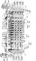
图1绘示三维可编程电阻存储阵列的2X2部分的示意图。其中,附图中的填充材料被移除,以提供构成三维阵列的半导体条纹与正交的字线的视图。在本附图中,仅显示两平面。然而,平面的数量可延伸至很多。如图1所示,存储阵列形成于集成电路衬底上,集成电路衬底具有绝缘层10在半导体或其它装置(未绘示)的下层。存储阵列包括多个被绝缘材料21、22、23与24分离的多个半导体条纹11、12、13与14的叠层。叠层为脊形且如附图中在Y轴上延伸,以使半导体条纹11-14可构为存储单元串。半导体串11与13可作为在第一存储平面中的存储单元串。半导体串12与14可作为在第二存储平面中的存储单元串。存储材料的层15,例如是反熔丝(anti-fuse)材料,在本实施例中涂布于多个半导体条纹的叠层,且在其它实施例中至少在半导体条纹的侧墙上。多个字线16、17正交设置于多个半导体条纹的叠层之上。字线16、17具有与这些半导体条纹的叠层共形的表面,填充被这些叠层定义的沟道(例如为20),并在叠层与字线16、17上的半导体条纹11-14的侧表面之间的交错点定义接口区的多层阵列。硅化物层18、19(例如为硅化钨、硅化钴或硅化钛)可形成于字线16、17的上表面之上。FIG. 1 is a schematic diagram of a 2×2 portion of a three-dimensional programmable resistance memory array. In the figures, the fill material is removed to provide a view of the semiconductor stripes and the orthogonal word lines forming the three-dimensional array. In this figure, only two planes are shown. However, the number of planes can be extended to many. As shown in FIG. 1, the memory array is formed on an integrated circuit substrate with an insulating
存储材料的层15可由反熔丝材料,例如是二氧化硅、氮氧化硅或其它氧化硅所组成。例如具有大约1到5纳米的厚度。也可以使用其它反熔丝材料例如为氮化硅。半导体条纹11-14可为具有第一导电材料(例如为P型)的半导体材料。字线16、17可为具有第二导电材料(例如为n型)的半导体材料。举例来说,半导体材料11-14可使用P型多晶硅制成,而字线16、17可使用相对n+型重掺杂制成。半导体条纹的宽度应提供足够的空间给空乏区(depletion region)以支持二极管操作。结果,存储单元包括整流器形成通过在阳极与阴极之间具有可编程反熔丝层的p-n接口形成,阳极与阴极形成于界在多晶硅条纹与线之间的交错点的三维阵列中。在其它实施例中,可使用不同的可编程电阻存储材料,包括过渡金属氧化物,例如氧化钨于钨之上或掺杂金属氧化半导体条纹。如此的材料可被编程与擦除,且可实施于每单元的存储多层比特(bits)操作。The
图2绘示存储单元的X-Z平面的剖面图,存储单元形成于字线16与半导体条纹14的交错处。主动区域25、26形成于条纹14的两侧壁上,条纹位于字线16与条纹14之间交错处。在原始状态,反熔丝层材料的层15具有高电阻。在编程后,反熔丝材料击穿,造成在反熔丝材料中的主动区域25、26两者或其中之一假设为低电阻状态。在本实施例中,每个存储单元具有二主动区域25、26,各位于半导体条纹14的各侧。图3绘示存储单元的X-Y平面的剖面图,存储单元形成于字线16、17与半导体条纹14的交错处。从字线的电流路径被通过字线16经过反熔丝材料的层15且下至半导体条纹14所定义。FIG. 2 is a cross-sectional view of the X-Z plane of the memory cell, which is formed at the intersection of the
电子电流如图3中通过实箭头绘制。电流从n+字线16至p型半导体条纹,且沿半导体条纹(--箭号)至感应放大器,感应放大器所在可测量以指出选择存储单元的状态。再依典型实施例中,使用大约1纳米氧化硅层作为反熔丝材料,编程脉冲可包括5至7伏特脉冲具有大约1百万分之一秒的脉冲宽度,应用于片上(on-chip)控制电路的控制,如图18所示。读取脉冲可包括具有由设置来确定脉宽的1至2伏特脉冲,应用于如下所述的片上控制电路的控制,请参照图18。读取脉冲可大幅小于编程脉冲。Electron currents are plotted by solid arrows in Fig. 3. Current flows from the
图4绘示各具有6单元的存储单元的2平面。存储单元通过二极管符号表示,且虚线表示介于阳极与阴极之间的反熔丝材料的层。存储单元的2平面定义在字线60、61的交错处,字线60、61作为第一字线WLn与第二字线WLn+1具有半导体条纹51、52的第一叠层、半导体条纹53、54的第二叠层、半导体条纹55、56的第三叠层作为在阵列的第一与第二层中的存储单元串n、n+1与n+2。存储单元的第一平面包括在半导体条纹52上的存储单元30、31,在半导体条纹54上的存储单元32、33,在半导体条纹56上的存储单元34、35。存储单元的第二平面包括在半导体条纹51上的存储单元40、41,在半导体条纹53上的存储单元42、43,在半导体条纹55上的存储单元44、45。如附图中所示,字线60作为字线WLn,包括重直延伸60-1、60-2、60-3对应于如图1中在叠层之间的沟道20中的材料,以沿着在每一平面中绘示的3半导体条纹耦合字线60至存储单元。一阵列具有许多层可被如本文说明实施,可使各个芯片有非常高的存储密度,且每个芯片接近或达到兆比特(terabits)。FIG. 4 shows 2 planes of memory cells each having 6 cells. The memory cell is represented by a diode symbol, and the dashed line represents the layer of antifuse material between the anode and cathode. The two planes of the memory cell are defined at the intersection of the word lines 60 and 61, and the word lines 60 and 61 as the first word line WLn and the second word
图5绘示三维电荷捕捉存储阵列的2X2部分的示意图。三维电荷捕捉存储阵列有填满的材料从附图中移除,以提供半导体条纹的叠层以及正交字线以构成三维阵列。在此附图中,仅显示2层。然而,层的数目可变为非常大的数目。如图5所示,存储阵列形成于集成电路衬底上,集成电路衬底具有绝缘层110位于下层的半导体或其它结构(未绘示)之上。存储阵列包括多个被绝缘材料121、122、123、124隔离的半导体条纹111、112、113、114的叠层(附图中绘示2个)。如附图中,叠层为脊形且延伸于Y轴上,以使半导体材料111-114可组为存储单元串。半导体条纹111与113在第一存储平面可作为存储单元串。半导体条纹112与114在第二存储平面可作为存储单元串。FIG. 5 is a schematic diagram of a 2×2 portion of a three-dimensional charge trapping memory array. The three-dimensional charge trapping memory array has the fill material removed from the figure to provide a stack of semiconductor stripes and orthogonal word lines to form the three-dimensional array. In this drawing, only 2 floors are shown. However, the number of layers can become a very large number. As shown in FIG. 5 , the memory array is formed on an integrated circuit substrate having an insulating layer 110 on an underlying semiconductor or other structure (not shown). The memory array comprises a plurality of stacks of semiconductor stripes 111 , 112 , 113 , 114 separated by insulating material 121 , 122 , 123 , 124 (two are shown in the figure). As shown in the figure, the stack is ridge-shaped and extends along the Y-axis so that the semiconductor materials 111-114 can be grouped into strings of memory cells. The semiconductor stripes 111 and 113 can serve as memory cell strings in the first memory plane. The semiconductor stripes 112 and 114 can serve as memory cell strings in the second memory plane.
在第一叠层中介于半导体条纹111与112之间的绝缘材料121,与在第二叠层中介于半导体条纹113与114之间的绝缘材料123具有大约或大于40纳米的有效氧化厚度(effective oxide thickness,EOT),有效氧化厚度为绝缘材料的厚度,此厚度根据二氧化硅的介电常数与选择的绝缘材料的介电常数的比例标准化。词汇“大约40纳米”在此处说明大约可有10%的变化,典型上用于制造此类型的结构。绝缘材料的厚度可扮演一关键角色于减少结构中邻近层的单元的干扰。在一些实施例中,当层之间达到充分的分离,绝缘材料的有效氧化厚度可大约为30纳米。The insulating material 121 between the semiconductor stripes 111 and 112 in the first stack and the insulating material 123 between the semiconductor stripes 113 and 114 in the second stack have an effective oxidation thickness of about or greater than 40 nanometers. oxide thickness, EOT), the effective oxide thickness is the thickness of the insulating material, which is standardized according to the ratio of the dielectric constant of silicon dioxide to the dielectric constant of the selected insulating material. The phrase "about 40 nanometers" is used here to describe that there may be a variation of about 10%, which is typically used to fabricate structures of this type. The thickness of the insulating material can play a key role in reducing interference between cells of adjacent layers in the structure. In some embodiments, when sufficient separation is achieved between the layers, the effective oxide thickness of the insulating material may be approximately 30 nanometers.
在本实施例中,存储材料的层115,例如是介电电荷捕捉结构,涂布于半导体条纹的多个叠层上。多个字线116、117正交设置于半导体条纹的多个叠层之上,填充被这些叠层定义的沟道(例如为120),并在叠层与字线116、117上的半导体条纹111-114的侧表面之间的交错点定义接口区的多层阵列。硅化物层118、119(例如为硅化钨、硅化钴或硅化钛)可形成于字线116、117上表面之上。In this embodiment, a layer 115 of memory material, such as a dielectric charge trapping structure, is coated on multiple stacks of semiconductor stripes. A plurality of word lines 116, 117 are arranged orthogonally over a plurality of stacks of semiconductor stripes, filling channels (eg, 120) defined by these stacks, and semiconductor stripes on the stacks and word lines 116, 117 The points of intersection between the side surfaces of 111-114 define a multilayer array of interface regions. Silicide layers 118 , 119 (eg, tungsten silicide, cobalt silicide, or titanium silicide) may be formed on top surfaces of the word lines 116 , 117 .
纳米导线金属氧化物半导体场效应管型单元也可以此方式配置,通过提供纳米导线或纳米管结构在字线111-114上的通道区域,如Paul等人在IEEE Transactions on Electron Devices,Vol.54,No.9,September 2007在“Impact of a Process Variation on Nanowire and Nanotube DevicePerformance”所描述,此文章将纳入作为参考。Nanowire Mosfet cells can also be configured in this way, by providing a channel region of nanowire or nanotube structure on the word lines 111-114, as Paul et al. in IEEE Transactions on Electron Devices, Vol.54 , No.9, September 2007 described in "Impact of a Process Variation on Nanowire and Nanotube Device Performance", this article is incorporated by reference.
结果,设置在与非门(NAND)快闪阵列中的硅氧化氮氧化硅型(SONOS-type)存储单元的三维阵列能够形成。源极、漏极与通道形成在硅半导体条纹111-114中,存储材料的层115包括隧穿介电层97、电荷存储层98与阻挡介电层99。隧穿介电层97其可由氧化硅形成。电荷存储层98其可由氮化硅形成。阻挡介电层(blocking dielectric layer)99可由氧化硅形成,且栅极包括字线116、117的多晶硅。As a result, a three-dimensional array of SONOS-type memory cells disposed in a NAND flash array can be formed. Sources, drains and channels are formed in the silicon semiconductor stripes 111 - 114 , and the layer 115 of memory material includes a tunneling dielectric layer 97 , a charge storage layer 98 and a blocking dielectric layer 99 . The tunneling dielectric layer 97 may be formed of silicon oxide. The charge storage layer 98 may be formed of silicon nitride. The blocking dielectric layer 99 may be formed of silicon oxide, and the gate comprises polysilicon of the word lines 116,117.
半导体条纹111-114可为p型半导体材料。字线116、117可为具有相同或不同的导电类型(例如为p+型)的半导体材料。举例来说,半导体条纹111-114可使用p型多晶硅或p型外延单结晶硅,而字线116、117可使用相对重掺杂p+型多晶硅制成。The semiconductor stripes 111-114 can be p-type semiconductor material. The word lines 116, 117 can be semiconductor materials with the same or different conductivity types (eg, p+ type). For example, the semiconductor stripes 111-114 can be made of p-type polysilicon or p-type epitaxial monocrystalline silicon, and the word lines 116, 117 can be made of relatively heavily doped p+-type polysilicon.
可选择地,半导体条纹111-114可为n型半导体材料。字线116、117可为相同或不同导电类型(例如为P+型)的半导体材料。n型条纹的设置造成内埋通道,空乏型电荷捕捉存储单元。举例来说,半导体条纹111-114可使用n型多晶硅或n型外延单结晶硅制成,而字线116、117可使用相对重掺杂p+多晶硅。典型于n型半导体条纹的掺杂浓度可大约为1018/cm3,有用的实施例可能在1017到1019/cm3的范围内。n型半导体条纹的使用特别在无界面(junction-free)实施例有利,以沿着与非门(NAND)串改善导电率,借此允许较高的读取电流。Optionally, the semiconductor stripes 111-114 can be n-type semiconductor material. The word lines 116 and 117 can be semiconductor materials of the same or different conductivity type (for example, P+ type). The arrangement of n-type stripes creates a buried channel and a depletion-type charge-trapping memory unit. For example, the semiconductor stripes 111-114 can be made of n-type polysilicon or n-type epitaxial monocrystalline silicon, and the word lines 116, 117 can be made of relatively heavily doped p+ polysilicon. Typical doping concentrations for n-type semiconductor stripes may be on the order of 1018 /cm3 , useful embodiments may be in the range of 1017 to 1019 /cm3 . The use of n-type semiconductor stripes is particularly advantageous in junction-free embodiments to improve conductivity along NAND strings, thereby allowing higher read currents.
因此,存储单元包括场效晶体管,场效晶体管具有电荷存储结构,电荷存储结构形成在交错点的三维阵列中。半导体条纹与字线的宽度大约为25纳米,脊形叠层之间的间隙大约为25纳米,装置具有几十层(例如为32层)可在单一芯片达到兆比特容量。Thus, the memory cell includes a field effect transistor having a charge storage structure formed in a three-dimensional array of interleaved points. The width of semiconductor stripes and word lines is about 25 nanometers, and the gap between the ridge stacks is about 25 nanometers. The device has dozens of layers (for example, 32 layers) to achieve megabit capacity in a single chip.
存储材料的层115可包括其它电荷存储结构。举例来说,带隙工程硅氧化氮氧化硅(BE-SONOS)电荷存储结构可使用在包括一隧穿介电层97,隧穿介电层97包括的材料组成形成倒转的“U”型价带于零偏压下。在一实施例中,隧穿介电层组成包括第一层、第二层与第三层。第一层被称为隧穿层,第二层被称为带偏移层(band offset layer),第三层被称为分离层。在本实施例中的层115的孔洞隧穿层包括二氧化硅于半导体条纹的侧表面上,其形成举例来说使用原位蒸汽产生(in-situ steam generation,ISSG)具有选择性的氮化(nitridation),在沉积期间通过一后沉积一氧化氮退火或通过一氧化氮的加成至环境。二氧化硅的第一层的厚度小于优选为


在本实施例中,带偏移层包括氮化硅在孔洞隧穿层上,其形成举例来说是在680℃使用例如是二氯硅烷与氨前趋物利用低压化学气相沉积形成,在另一可选择的程序,带偏移层包括氮氧化硅,以使用具有一氧化二氮(N2O)前趋物的相似程序制成。氮化硅的带偏移层厚度小于
在本实施例中,隔离层包括二氧化硅,位在氮化硅的带偏移层上,其形成举例来说使用低压化学气相沉积高温氧化沉积。二氧化硅的隔离层的厚度小于

在第一位置的价带能量水平(valence band energy level)使得电场足以诱导孔洞隧穿经过薄区域,薄区域介于半导体与第一位置的接口。在第一位置的价带能量水平也足以在第一位置,有效消去在第一位置之后的组成隧穿介电中的孔洞隧穿屏障后提升价带能量水平。此结构在三层隧穿介电层中建立倒转U型价带能量水平,且在没有电场或为其它操作目的诱发较小的电场下,例如从单元读取数据或编程相邻单元,当有效避免电荷经过混合隧穿介电质泄漏时,结构使电场辅助孔洞(electric field assistedhole)在高速下隧穿。The valence band energy level at the first site is such that the electric field is sufficient to induce hole tunneling through the thin region interposed between the interface of the semiconductor and the first site. The energy level of the valence band at the first position is also sufficient to increase the energy level of the valence band after effectively eliminating the tunneling barrier of holes in the tunneling dielectric behind the first position at the first position. This structure establishes an inverted U-shaped valence band energy level in the triple tunneling dielectric layer and induces a smaller electric field in the absence of an electric field or for other operational purposes, such as reading data from a cell or programming an adjacent cell, when active To avoid charge leakage through the hybrid tunneling dielectric, the structure enables electric field assisted holes to tunnel at high speeds.
在本装置中,存储材料的层115包括带隙工程混合隧穿介电层(bandgap engineered composite tunneling dielectric layer),带隙工程混合隧穿介电层包括二氧化硅层的厚度小于2纳米,氮化硅层的厚度小于3纳米,且二氧化硅层小于4纳米。在一实施例中,混合隧穿介电层由超薄氧化硅层O1(例如小于等于


在本实施例中,存储材料的层115中的电荷捕捉层包括具有大于

在本实施例中,存储材料的层115中的阻挡介电层包括具有大于

在一实施例中,孔洞隧穿层可为


图6绘示形成于字线116与半导体条纹114的交界处的电荷捕捉存储单元于X-Z平面的剖面图。主动电荷捕捉区域125、126形成在介于字线116与条纹114之间的条纹114的二侧面上。本文说明的实施例中,如图6所示,各存储单元具有主动电荷存取区域125、126的双栅极场效晶体管,各位于半导体条纹114的各侧边。电流如附图所绘的实箭头沿着p型半导体条纹流动,以感应放大器,放大器可被测量以显示选择的存储单元的状态。FIG. 6 is a cross-sectional view of the charge trapping memory cell formed at the junction of the word line 116 and the semiconductor stripe 114 along the X-Z plane. Active charge trapping regions 125 , 126 are formed on two sides of the stripe 114 between the word line 116 and the stripe 114 . In the embodiment described herein, as shown in FIG. 6 , each memory cell has dual gate field effect transistors with active charge access regions 125 , 126 located on respective sides of the semiconductor stripe 114 . Current flows along the p-type semiconductor stripes as depicted by solid arrows to sense amplifiers that can be measured to reveal the state of selected memory cells.
图7绘示形成于字线116、117与半导体条纹114的交界处的电荷捕捉存储单元于X-Y平面的剖面图。绘示电流于半导体条纹114向下。位于字线116、117之间的源极/漏极区域128、129、130可为“无界面(junction-free)”,源极与漏极掺杂没有具有相反于字线之下的通道区域的导电类型的导电类型。在无介面实施例中,电荷捕捉场效晶体管可具有p型通道结构。同样地,在字线定义之后于自我对准注入中,源极与漏极掺杂可实施于一些实施例中。7 shows a cross-sectional view of the charge trapping memory cell formed at the junction of the word lines 116, 117 and the semiconductor stripe 114 on the X-Y plane. Current is shown down the semiconductor stripe 114 . The source/drain regions 128, 129, 130 located between the wordlines 116, 117 may be "junction-free", with the source and drain doping not having the opposite channel region below the wordlines The conductivity type of the conductivity type. In an interfaceless embodiment, the charge trapping field effect transistor may have a p-channel structure. Likewise, source and drain doping may be implemented in some embodiments in a self-aligned implant after wordline definition.
在另一实施例中,半导体条纹111-114可使用无介面设置的轻掺杂n型半导体实施,造成内埋通道场效晶体管可操作于空乏模式(depletionmode),自然偏移低于用于电荷捕捉单元的临界分布。In another embodiment, the semiconductor stripes 111-114 can be implemented using a lightly doped n-type semiconductor without interfacing, so that the buried channel field effect transistor can be operated in a depletion mode, and the natural shift is lower than that used for the charge Captures the critical distribution of cells.
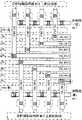
图8绘示设置于与非门组态中具有9电荷捕捉单元的存储单元的2平面。与非门组态以立方体(cube)表示,立方体可包括许多平面与许多字线。存储单元的2平面定义在字线160、161的交错点作为半导体条纹的第一叠层、半导体条纹的第二叠层、半导体条纹的第三叠层的字线WLn-1、WLn。Figure 8 shows 2 planes of memory cells with 9 charge trapping cells arranged in a NAND configuration. The NAND gate configuration is represented by a cube, which may include many planes and many word lines. Two planes of the memory cell are defined at the intersection of
存储单元的第一平面包括存储单元70、71在半导体条纹上的与非门串中,存储单元73、74在半导体条纹上的与非门串中,存储单元76、77在半导体条纹上的与非门串中。各与非门串连接于一接地选择晶体管的其一侧(例如为接地选择装置90、72于与非门串70、71的其一侧上)。The first plane of memory cells includes
在一实施例中,存储单元的第二平面对应于一立方体的底面,且包括存储单元(例如为80、82、84)设置于与非门串中相似于第一平面中的方法。In one embodiment, the second plane of memory cells corresponds to the bottom of a cube and includes a method in which memory cells (such as 80, 82, 84) are arranged in NAND gate strings similar to the first plane.
如图所示,字线161作为字线WLn包括垂直延伸对应于图5中在沟道120中介于叠层间的材料,为了耦合字线161至所有平面中的半导体条纹之间的沟道的接口区中的存储单元(第一平面中的单元71、74、77)。As shown,
存储单元串在相邻叠层的交替端,位于位线端到源极线端位向与源极线端到位线端位向之间。The memory cell strings are at alternate ends of adjacent stacks, between the bit line end to the source line end orientation and the source line end to the bit line end orientation.
位线BLn与BLn-1终止存储单元串,邻接于串选择装置。举例来说,在最高存储平面中,位线BLn终止存储单元串,存储单元串具有串选择晶体管96与98。相较之下,位线未连接于接触线(trace)97,因为相邻叠层交替端的串,位于位线端到源极线端位向与源极线端到位线端位向之间。因此取代此串,对应的位线连接于串的另一端。在存储平面的底,位线BLn-1终止具有对应串选择晶体管的存储单元串。Bit lines BLn and BLn-1 terminate the string of memory cells adjacent to the string selection device. For example, in the uppermost storage plane, bit line BLn terminates a string of memory cells, which has string
串选择晶体管96、98连接于分别的与非门串与串选择线SSLn-1与SSLn之间的设置。类似地,相似的串选择晶体管在立方体中的底面上且连接于此设置的各与非门串与串选择线SSLn-1与SSLn之间。串选择线106、108连接于不同的脊与各存储单元串中串选择晶体管的栅极,且在本实施例中提供选择信号SSLn-1、SSLn与SSLn+1。String
相反地,因为位于位线端到源极线端位向与源极线端到位线端位向之间的相邻叠层交替端的串,串选择晶体管并非连接接触线97。因此取代此串,对应串选择晶体管连接于串的另一端。具有存储单元73、74的与非门串也具有串选择装置于串的另一端上,但未显示。接触线97通过源极线107终止。Conversely, string select transistors are not connected to contact line 97 because of the strings at alternate ends of adjacent stacks between the bit line end to source line end orientation and the source line end to bit line end orientation. Therefore instead of this string, the corresponding string select transistor is connected to the other end of the string. The string of NAND gates with
接地选择晶体管90-95设置于与非门串的第一端。接地选择晶体管72、75、78与对应第二平面接地选择晶体管设置在与非门串的第二端。因此,接地选择晶体管位于存储串的两端上。依据存储串的特别端,接地选择晶体管耦合存储串至源极线或至串选择装置及位线。The ground selection transistors 90-95 are disposed at the first end of the NAND gate string. The
在本实施例中,接地选择信号159耦合至接地选择晶体管90-95的栅极,且可以如字线160、161的相同方式实施。在一些实施例中,串选择晶体管与接地选择晶体管可使用相同介电叠层,作为栅极氧化物作为存储单元。在其它实施例中,使用典型的栅极氧化物代替。同样地,通道长度与宽度调整至设计者的需求以提供晶体管开关函数(switching function)。In this embodiment, ground
图9为相似于图5的另一结构。在图中相似结构的符号再次使用于附图中,且不再说明。图9不同于图5在绝缘层110的表面110A以及半导体条纹113、114的侧表面113A与114A暴露于作为字线的字线116之间,由刻蚀工艺形成字线。因此,存储材料层115在无伤害操作下完全地或部分地于字线间刻蚀。然而,在一些结构中没有必要如上所述的刻蚀穿越存储层115形成介电电荷捕捉结构。FIG. 9 is another structure similar to FIG. 5 . Symbols for similar structures in the figures are used again in the figures and will not be described again. 9 is different from FIG. 5 in that the surface 110A of the insulating layer 110 and the side surfaces 113A and 114A of the semiconductor stripes 113 and 114 are exposed between the word line 116 as the word line, and the word line is formed by an etching process. Therefore, the memory material layer 115 is completely or partially etched between the word lines in a harmless operation. However, in some structures it is not necessary to etch through the storage layer 115 to form the dielectric charge trapping structure as described above.
图10为类似于图6于X-Z平面中的存储单元的剖面图。图10与图6一样,绘示类似图9的结构形成存储单元,存储单元与图5实施的剖面图的结构相同。图11绘示相似于图7于X-Y平面中的存储单元的剖面图。图11相异于图7在沿半导体条纹114的侧表面(例如为114A)的区域128a、129a与130a中可移除存储材料。FIG. 10 is a cross-sectional view of the memory cell in the X-Z plane similar to FIG. 6 . FIG. 10 is the same as FIG. 6 , showing a structure similar to that of FIG. 9 forming a memory cell, and the structure of the memory cell is the same as the cross-sectional view implemented in FIG. 5 . FIG. 11 shows a cross-sectional view of the memory cell in the X-Y plane similar to FIG. 7 . FIG. 11 is different from FIG. 7 in that the memory material can be removed in regions 128 a , 129 a and 130 a along the side surface (eg, 114A) of the semiconductor stripe 114 .
图12-图16绘示用于实施如上所述的三维存储阵列的基本程序流程的阶段,仅利用二用于形成阵列的关键对准步骤的图案化掩膜步骤。在图12中,绘示的结构为由绝缘层210、212、214与半导体层211、213交替沉积,半导体层211、213使用掺杂半导体例如在芯片的阵列面积的毡毯状沉积(blanket deposition)中。依据注入,半导体层211、213可使用具有n型或p型掺杂的多晶硅或外延单层结晶硅实施。内层绝缘层210、212、214举例来说使用二氧化硅、其它氧化硅或氮化硅以实施。这些层可以不同的方式形成,包括低压化学沉积程序可用在此工艺。12-16 illustrate the stages of a basic process flow for implementing a three-dimensional memory array as described above, utilizing only two patterning masking steps for the critical alignment steps of forming the array. In FIG. 12 , the illustrated structure is alternately deposited by insulating
图13绘示第一光刻蚀图案化步骤的结果,用于定义多个半导体条纹的脊型叠层250,半导体条纹使用半导体层211、213的材料实施,且被绝缘层212、214隔开。深且高的高宽比(aspect ratio)沟道可被形成于叠层中,支撑许多层,应用碳硬掩膜(hard mask)以及反应离子刻蚀以使用光刻蚀基底程序。FIG. 13 shows the result of a first photolithographic patterning step for defining a ridge stack 250 of a plurality of semiconductor stripes implemented using the material of
虽然未绘示,在步骤中存储串的交替位向定义位线端到源极线端位向以及源极线端到位线端位向。Although not shown, the alternate orientations of the strings in the steps define the bitline-to-sourceline-terminal orientation and the source-line-to-bitline-terminal orientation.
图14A与图14B分别绘示一实施例中的下一个步骤,包括编程电阻存储结构,例如反熔丝单元结构,与一实施例包括编程电荷捕捉存储装置,例如硅氧化氮氧化硅型存储单元结构。14A and 14B respectively illustrate the next step in an embodiment including programming a resistive memory structure, such as an antifuse cell structure, and an embodiment including programming a charge trapping memory device, such as a silicon-oxynitride-silicon-type memory cell. structure.
在实施例中,图14A绘示存储材料层215的毡毯状沉积的结果,其中存储材料由单层例如相似于图1所绘示反熔丝结构的例子所组成。在另一实施例中,相比于毡毯状沉积,可实施一氧化程序以形成氧化物于半导体条纹暴露的侧边,氧化物作为存储材料。In an embodiment, FIG. 14A shows the result of a blanket deposition of a
图14B显示层315的毡毯状沉积结果,包括多层电荷捕捉结构,包括隧穿层397、电荷捕捉层398以及阻挡层399,如图4所述。如图14A与图14B绘示,存储层215、315以共形的方式沉积于半导体条纹的脊形叠层之上(图13的250)。FIG. 14B shows the result of blanket deposition of
图15绘示高的高宽比填充步骤的结果,其中导电材料例如是具有n型或p型掺杂多晶硅,用于字线作为字线沉积以形成层225。同样地,硅化物226的层可在实施例中形成于层225之上,其中利用多晶硅。如附图所绘示,高的高宽比沉积技术例如是在实施例中多晶硅的低压化学沉积用来完整地填充脊形叠层之间的沟道220。甚至是非常窄的沟道例如10纳米宽的高的高宽比。FIG. 15 shows the result of a high aspect ratio fill step in which a conductive material such as polysilicon with n-type or p-type doping is deposited as wordlines to form
图16绘示第二光刻蚀图案化步骤的结果,第二光刻蚀图案化步骤用于定义多个位线260作为3维存储阵列的位线。使用多晶硅对氧化硅或氮化硅高刻蚀比的刻蚀工艺刻蚀多晶硅。因此,使用交替刻蚀程序,依靠相同掩膜刻蚀半导体与绝缘体层,程序停止于下层绝缘层210上。FIG. 16 shows the results of the second photolithographic patterning step used to define a plurality of
在此步骤,接地选线也可以被定义,在此步骤中,虽然栅极结构共形于个别半导体条纹叠层,栅极结构可被串选择线控制也可以被定义。In this step, ground select lines can also be defined. In this step, although gate structures are conformal to individual semiconductor stripe stacks, gate structures controlled by string select lines can also be defined.
选择性制造步骤包括形成硬掩膜于多个字线之上,且硬掩膜于栅极结构之上。硬掩膜可使用可阻挡离子注入程序的相对厚的氮化硅或其它材料层形成。在硬掩膜形成后,可施加注入以增加半导体条纹中的掺杂浓度,且在阶梯结构中,因而减少沿半导体条纹电流路径的电阻。通过利用控制注入能量,注入可穿透到半导体条纹的底,与在叠层中各迭加的半导体条纹。An optional fabrication step includes forming a hard mask over the plurality of word lines, and a hard mask over the gate structure. The hard mask may be formed using a relatively thick layer of silicon nitride or other material that blocks the ion implantation process. After the hard mask is formed, an implant can be applied to increase the doping concentration in the semiconductor stripes and, in a stepped structure, thus reduce the resistance of the current path along the semiconductor stripes. By using controlled implant energy, the implant can penetrate to the bottom of the semiconductor stripes, and to each superimposed semiconductor stripe in the stack.
随后,移除硬掩膜,沿着字线的上表面与栅极结构之上,暴露硅化物。在一层间介电体形成于阵列的顶部的上后,打通接触拴塞(plug)的孔洞(vias),例如以钨填满,形成以抵达至栅极结构的上表面。上覆金属线被图案化以连接串选择线至行译码器电路。建立三平面译码网络使用一字线、一位线与一串选择线存取选择单元。可参照美国专利号码6,906,940,Plane Decoding Method and Device for Three Dimensional Memories。Subsequently, the hard mask is removed to expose the silicide along the upper surface of the word line and above the gate structure. After an ILD is formed on top of the array, vias for contact plugs, eg filled with tungsten, are formed to reach the top surface of the gate structure. Overlying metal lines are patterned to connect the string select lines to the row decoder circuit. A three-plane decoding network is constructed using a word line, a bit line and a string of select lines to access select cells. See US Patent No. 6,906,940, Plane Decoding Method and Device for Three Dimensional Memories.
图17为由透射电子显微镜显示制作与测试8层垂直栅极、薄膜晶体管、带隙工程硅氧化氮氧化硅电荷捕捉与非门装置的一部份的剖面图。装置具有75纳米的半间距。通道为n型多晶硅大约18纳米厚。无使用额外交界注入,形成无介面结构。介于条纹之间的绝缘材料用于隔绝在z轴方向中的通道为大约40纳米厚的二氧化硅。栅极通过p+多晶硅线提供。串选择线与接地选择线装置具有的通道长度长于存储单元。测试装置实施32字线,无介面与非门串。第30图中下条纹的宽度大于上条纹的宽度,因为用沟道刻蚀形成结构造成锥形侧墙,渐渐地当沟道变深条纹就变宽,且介于条纹之间的绝缘材料比多晶硅被刻蚀的多。Fig. 17 is a cross-sectional view showing a part of fabrication and testing of 8-layer vertical gate, thin film transistor, bandgap engineered silicon oxynitride silicon oxynitride charge trapping NAND gate device by transmission electron microscope. The device has a half-pitch of 75 nm. The channel is n-type polysilicon approximately 18 nanometers thick. No additional interface injection is used to form an interface-less structure. The insulating material between the stripes used to isolate the channel in the z-axis direction is approximately 40 nm thick silicon dioxide. The gate is provided by a p+ polysilicon line. The string selection line and the ground selection line arrangement have a channel length longer than that of the memory cell. The test set implements 32 word lines with no interface NAND strings. The width of the lower stripes in Figure 30 is greater than that of the upper stripes, because the structure is formed by trench etching to form a tapered sidewall, and gradually the stripes become wider when the trenches become deeper, and the insulating material between the stripes is less than that of the upper stripes. Polysilicon is etched more.
图18为依据本发明的一实施例的简单的集成电路的方块图。集成电路线875包括三维编程电阻存储阵列(RRAM)860如本文说明实施,在一半导体衬底上,具有位线端到源极线端位向与源极线端到位线端位向的交替存储串位向,且每隔一叠层上叠层的其一端具有串选择线栅极结构。列译码器861耦合至多个字线862,且在存储阵列860中沿着列设置。行译码器863耦合多个串选择线864沿着行设置,这些行对应于存储阵列860中的叠层,用于从阵列860中的存储单元读取及编程数据。平面译码器858耦合多个在位线859上的存储阵列860中的平面。存取应用于总线865至行译码器863、列译码器861与平面译码器858。在本实施例中,感应放大器与数据输入结构于集区866中经由数据总线867耦合行译码器863。数据经由数据输入线871从集成电路875上的输入/输出端口或从其它内部于或外部于集成电路875数据的数据源至集区866中的数据输入结构提供。在一实施例中,其它电路系统874包括于集成电路上,例如为通用处理器(general purpose processor)或特用应用电路系统,或通过编程电阻单元阵列支持提供系统单芯片(system-on-a-chip)功能的模块的组合。数据经由数据输出线872从集区(block)866中的感应放大器至在集成电路875上的输入/输出端口,或至其它内部或外部于集成电路875的数据终点。Figure 18 is a block diagram of a simple integrated circuit according to one embodiment of the present invention. Integrated
在一实施例中,控制器的实施使用偏压设置状态机器(biasarrangement state machine)869控制偏压设置提供电压的应用,此应用经由在集区868中的电压提供或提供器以产生或提供,例如为读取或编程电压。控制器可使用该领域的普通技术人员所知的特用逻辑电路系统实施。在另一实施例中,控制器包括一通用处理器,其可实施于相同的集成电路上,此集成电路执行计算机编程以控制或操作装置。再一实施例中,可利用特用逻辑电路系统与通用处理器的组合于控制器的实施。In one embodiment, an implementation of the controller uses a bias
图19为依据本发明的一实施例的简单的集成电路的方块图。集成电路线975包括三维与非门闪存960如本文说明实施,在一半导体衬底上,具有位线端到源极线端位向与源极线端到位线端位向的交替存储串位向,且每隔一叠层上叠层的其一端具有串选择线栅极结构。列译码器961耦合至多个字线962,且在存储阵列960中沿着列设置。行译码器963耦合多个串选择线964沿着行设置,这些行对应于存储阵列960中的叠层,用于从阵列960中的存储单元读取及编程数据。平面译码器958耦合多个经由位线959上的存储阵列860中的平面。存取应用于总线965至行译码器963、列译码器961与平面译码器958。在本实施例中,感应放大器与数据输入结构于集区966中经由数据总线967耦合行译码器963。数据经由数据输入线971从集成电路975上的输入/输出端口或从其它内部于或外部于集成电路975数据的数据源至集区966中的数据输入结构提供。在一实施例中,其它电路系统974包括于集成电路上,例如为通用处理器(generalpurpose processor)或特用应用电路系统,或通过与非门快闪存储单元阵列支持提供系统单芯片(system-on-a-chip)功能的模块的组合。数据经由数据输出线972从集区966中的感应放大器至在集成电路975上的输入/输出端口,或至其它内部或外部于集成电路975的数据终点。Figure 19 is a block diagram of a simple integrated circuit according to one embodiment of the present invention. Integrated
在一实施例中,控制器的实施使用偏压设置状态机器(biasarrangement state machine)969控制偏压设置提供电压的应用,此应用经由在集区968中的电压提供或提供器以产生或提供,例如为读取、擦除、编程、擦除确认或编程确认电压。控制器可使用该领域的普通技术人员所知的特用逻辑电路系统实施。在另一实施例中,控制器包括一通用处理器,其可实施于相同的集成电路上,此集成电路执行计算机编程以控制或操作装置。再一实施例中,可利用特用逻辑电路系统与通用处理器的组合于控制器的实施。In one embodiment, the implementation of the controller uses a bias
图20-图22绘示第一三维与非门闪存阵列结构,具有连续较高的串选择线的金属层,具有纵长位向平行于半导体材料条纹,串选择线具有横向位向平行于字线,且位线具有纵向位向平行于半导体材料条纹。20-22 illustrate the first three-dimensional NAND gate flash memory array structure, which has a metal layer with continuous higher string selection lines, has a longitudinal direction parallel to the semiconductor material stripes, and a string selection line has a lateral direction parallel to the word line, and the bit line has a longitudinal direction parallel to the semiconductor material stripe.
图20为第一三维与非门闪存阵列结构的示意图。绝缘材料从附图中移除以暴露出额外的结构。举例来说,移除介于半导体条纹之间、脊形叠层中以及介于半导体条纹的脊形叠层之间的绝缘层。FIG. 20 is a schematic diagram of the structure of the first three-dimensional NAND flash memory array. Insulation material has been removed from the figures to expose additional structures. For example, insulating layers between semiconductor stripes, in ridge stacks, and between ridge stacks of semiconductor stripes are removed.
多层阵列形成于绝缘层之上,且包括多个字线425-1、...、425-n-1、425-n共形于多个脊形叠层,且作为字线WLn、WLn-1、...、WL1。多个脊形叠层包括半导体条纹412、413、414与415。在相同平面中的半导体条纹通过阶梯结构电性耦合。The multi-layer array is formed on the insulating layer, and includes a plurality of word lines 425-1, . -1,...,WL1. The plurality of ridge stacks includes
显示的字线符号从1增加至N为从整体结构的后面到前面,施予双数存储页数。对于单数存储页数,字线符号从N减少到1为从整体结构的后面到前面。The displayed word line symbols increase from 1 to N to give an even number of memory pages from the back to the front of the overall structure. For a single number of memory pages, word line symbols are reduced from N to 1 from the back to the front of the overall structure.
阶梯结构412A、413A、414A、415A终止半导体条纹,例如为半导体条纹412、413、414、415。如图所示,阶梯结构412A、413A、414A、415A电性连接于不同的位线用于连接至译码电路系统以在阵列中选择平面。阶梯结构412A、413A、414A、415A可在同时间被图案化以定义多个脊形叠层。The stepped
阶梯结构402B、403B、404B、405B终止半导体条纹,例如为半导体条纹402、403、404、405。如图所示,阶梯结构402B、403B、404B、405B电性连接于不同的位线用于连接至译码电路系统以在阵列中选择平面。阶梯结构402B、403B、404B、405B可在同时间被图案化以定义多个脊形叠层。The stepped
任何半导体条纹的叠层为耦合阶梯结构412A、413A、414A、415A或阶梯结构402B、403B、404B、405B,并非耦合两者。半导体条纹的叠层具有二相反位向其中之一,二相反位向为位线端至源极线端位向或源极线端到位线端位向。举例来说,半导体条纹412、413、414、415的叠层具有位线端至源极线端位向,且半导体条纹402、403、404、405的叠层具有源极线端至位线端位向。Any stack of semiconductor stripes is coupled to either the stepped
半导体条纹412、413、414、415的叠层为通过阶梯结构412A、413A、414A、415A终止于一端,并通过串选择线栅极结构419、栅极选择线426、字线425-1WL至425-NWL、栅极选择线427以及通过源极线428终止于另一端。半导体条纹412、413、414、415的叠层未抵达阶梯结构402B、403B、404B、405B。The stack of
半导体条纹402、403、404、405的叠层为通过阶梯结构402B、403B、404B、405B终止于一端,并通过串选择线栅极结构409、栅极选择线427、字线425-N至425-1、栅极选择线426以及通过源极线428终止于另一端(被附图中其它部分遮盖)。半导体条纹402、403、404、405的叠层未抵达阶梯结构412A、413A、414A、415A。The stack of
存储材料层分离字线425-1至425-n,从半导体条纹412-415以及402-405,如上述的附图所详细说明。接地选择线426与427共形于多个脊形叠层,相似于字线。The layer of memory material separates the word lines 425-1 to 425-n from the semiconductor stripes 412-415 and 402-405, as described in detail in the aforementioned figures. Ground
各半导体的叠层通过阶梯结构终止于一端,且通过源极线终止于另一端。举例来说,半导体条纹412、413、414、415的叠层通过阶梯结构412A、413A、414A、415A终止,且通过源极线428终止另一端。在附图的近端,每隔一半导体条纹的叠层为通过阶梯结构402B、403B、404B、405B终止,且每隔一半导体结构通过分离源极线终止。在附图的远端,每隔一半导体条纹的叠层为通过阶梯结构412A、413A、414A、415A终止,且每隔一半导体结构通过分离源极线终止。Each stack of semiconductors is terminated at one end by a staircase structure and at the other end by a source line. For example, the stack of
位线与串选择线形成于金属层ML1、ML2与ML3,且以下以优选视角的附图显示。Bit lines and string select lines are formed on metal layers ML1, ML2, and ML3, and are shown in the figures below with preferred perspectives.
晶体管形成于阶梯结构412A、413A、414A与字线425-1之间。在晶体管中,半导体条纹(例如为413)作为装置的通道区域。串选择线栅极结构(例如为419、409)为在定义字线425-1至425-n的相同步骤中图案化。硅化物426的层可沿字线与接地选择线的上表面、且于栅极结构429之上形成。存储材料415的层可作为晶体管的栅极介电层。晶体管作为串选择栅耦合于译码电路系统用于在阵列中选择特别脊形叠层。Transistors are formed between the
图21与图22中为图20中第一三维与非门闪存阵列结构的侧面示意图。图21绘示所有的三金属层ML1、ML2与ML3。图22绘示较低的二金属层ML1与ML2,移除ML3以使视角更清楚。FIG. 21 and FIG. 22 are schematic side views of the structure of the first three-dimensional NAND flash memory array in FIG. 20 . FIG. 21 shows all three metal layers ML1 , ML2 and ML3 . FIG. 22 shows the lower two metal layers ML1 and ML2, with ML3 removed for a clearer viewing angle.
第一金属层ML1包括串选择线具有纵向位向平行于半导体材料条纹。这些ML1串选择线通过短孔洞连接至不同的串选择线栅极结构(例如为409、419)。The first metal layer ML1 includes string selection lines having a longitudinal orientation parallel to the semiconductor material stripes. These ML1 string select lines are connected to different string select line gate structures (
第二金属层ML2包括串选择线具有纵向位向平行于字线。这些ML2串选择线通过短孔洞连接至不同的ML1串选择线。The second metal layer ML2 includes string selection lines having a longitudinal direction parallel to the word lines. These ML2 string selection lines are connected to different ML1 string selection lines through short holes.
在组合上,这些ML1串选择线与ML2串选择线允许串选择线信号去选择一特定的半导体条纹的叠层。In combination, these ML1 string select lines and ML2 string select lines allow the string select line signals to select a particular stack of semiconductor stripes.
第一金属层ML1还包括二源极线,具有纵向位向平行于字线The first metal layer ML1 also includes two source lines, with a vertical direction parallel to the word line
最后,第三金属层ML3包括位线具有纵向位向平行于半导体材料条纹。不一样的位线电性连接于不一样的阶梯结构412A、413A、414A、415A与402B、403B、404B、405B的步阶。这些ML3位线允许位线信号去选择一特定半导体条纹的水平平面。Finally, the third metal layer ML3 includes bit lines with a longitudinal orientation parallel to the semiconductor material stripes. Different bit lines are electrically connected to steps of
因为特定字线允许字线去选择一特定存储单元的列平面,此字线信号的三倍组合,位线信号、以及串选择线信号足以从存储单元的三维阵列选择一特定存储单元。Because the specific word line allows the word line to select a specific memory cell column plane, the triple combination of the word line signal, the bit line signal, and the string select line signal is sufficient to select a specific memory cell from the three-dimensional array of memory cells.
图23-图26绘示第二三维与非门闪存阵列结构,具有连续较高的串选择线的金属层,具有横向位向平行于字线,具有纵向位向平行于半导体材料条纹且位线具有纵向位向平行于半导体材料条纹。23-26 illustrate the second three-dimensional NAND flash memory array structure, which has a metal layer with continuous higher string selection lines, has a lateral orientation parallel to the word lines, and has a vertical orientation parallel to the semiconductor material stripes and the bit lines. Stripes with a longitudinal orientation parallel to the semiconductor material.
第二三维与非门闪存阵列绘示于图23-图26大幅相似于第一三维与非门闪存阵列绘示于图20-图22。图26更移除所有三金属层ML1、ML2、ML3以得到更佳视角。The second 3D NAND flash array shown in FIGS. 23-26 is substantially similar to the first 3D NAND flash array shown in FIGS. 20-22 . In FIG. 26, all three metal layers ML1, ML2, and ML3 are removed to obtain a better viewing angle.
然而,当第一三维与非门闪存阵列绘示于图20-图22显示八字线,第二三维与非门闪存阵列绘示于第23-26图显示三十二字线。其它实施例具有不同的字线、位线与串选择线的标号,且对应不同半导体条纹叠层的不同标号等等。However, while the first 3D NAND flash memory array is shown in FIGS. 20-22 showing eight word lines, the second 3D NAND flash memory array is shown in FIGS. 23-26 showing thirty-two word lines. Other embodiments have different labeling of wordlines, bitlines, and string select lines, corresponding to different labeling of different semiconductor stripe stacks, and so on.
同样地,尽管第一三维与非门闪存阵列绘示于图20-图22显示金属接触拴塞连接ML3位线至阶梯结构的不同步阶,第二三维与非门闪存阵列绘示于图23-图26显示连接金属接触拴塞至阶梯结构的不同步阶,伴随多晶硅拴塞。Likewise, although the first 3D NAND flash array is shown in FIGS. 20-22 showing metal contact plugs connecting the ML3 bit line to different steps of the ladder structure, the second 3D NAND flash array is shown in FIG. 23 - Figure 26 shows the different steps connecting the metal contact plugs to the stepped structure, with polysilicon plugs.
更进一步,尽管第一三维与非门闪存阵列绘示于图20-图22显示具有在ML2引导至译码器的串选择线,以及于ML1上引导至串选择线栅极结构的串选择线。第二三维与非门闪存阵列绘示于图23-图26显示具有在ML1引导至译码器的串选择线,以及于ML2上引导至串选择线栅极结构的串选择线。Furthermore, although the first 3D NAND flash memory array is shown in Figure 20-Figure 22 shows a string selection line with a string selection line leading to the decoder at ML2, and a string selection line leading to the string selection line gate structure on ML1 . The second 3D NAND flash memory array is shown in FIGS. 23-26 with string select lines leading to the decoder on ML1 and string select lines leading to the string select line gate structure on ML2.
图27-图31为图20-图22的第一三维与非门闪存阵列结构的设计示意图,具有不同的偏压设置。FIGS. 27-31 are schematic design diagrams of the first three-dimensional NAND flash memory array structure in FIGS. 20-22 , with different bias settings.
在图27的设计示意图中,半导体条纹的叠层显示为具有点破折号边界的垂直条纹。半导体条纹的相邻叠层交替于相反位向之间,相反位向有位线端到源极线端位向与源极线端到位线端位向。每隔一半导体条纹的叠层从在顶处的位线结构到在底处的源极线结构。每隔一半导体条纹的叠层从在顶处的源极线结构到在底处的位线结构。In the design schematic of Figure 27, the stack of semiconductor stripes is shown as vertical stripes with dot-dash boundaries. Adjacent stacks of semiconductor stripes alternate between opposite orientations, bit line end to source line end orientation and source line end to bit line end orientation. The stack of every other semiconductor stripe goes from a bit line structure at the top to a source line structure at the bottom. The stack of every other semiconductor stripe goes from a source line structure at the top to a bit line structure at the bottom.
覆盖于半导体条纹的叠层为水平字线与水平接地选择线(双)与接地选择线(单)。也覆盖于半导体条纹的叠层为串选择线栅极结构。串选择线栅极结构在半导体条纹的底端覆盖每隔一半导体条纹的叠层。在另一案例中,串选择线栅极结构控制电性连接任何半导体条纹叠层与叠层的对应位线接触结构。The stacks covering the semiconductor stripes are horizontal word lines and horizontal ground select lines (dual) and ground select lines (single). The stack that also covers the semiconductor stripes is a string select line gate structure. The string selection line gate structure covers every second stack of semiconductor stripes at the bottom of the semiconductor stripes. In another example, the string select line gate structure controls to electrically connect any semiconductor stripe stack to a corresponding bit line contact structure of the stack.
显示的字线标号,从1增加至N为从附图的顶处到底处,施予双数存储页数。对于单数存储页数,字线符号从N减少到1为从附图的底处到顶处。The word line numbers shown, increasing from 1 to N, are given from top to bottom of the drawing, giving even numbers of memory pages. For singular memory page numbers, the word line symbols decrease from N to 1 from the bottom to the top of the figure.
覆盖字线、接地选择线与串选择线栅极结构为垂直地ML1SSL串选择线。覆盖ML1SSL串选择线为水平地ML2SSL串选择线。虽然ML2SSL串选择线显示终止于对应的ML1SSL串选择线用于更易看清结构,ML2SSL串选择线可在水平上更长。ML2SSL串选择线从译码器传输信号,且ML1SSL串选择线耦合这些译码器信号至特定串选择线栅极结构以选择特定的半导体条纹的叠层。Overlaying the word line, the ground select line and the string select line gate structure is the vertical ML1SSL string select line. Override the ML1SSL string select line for the horizontally grounded ML2SSL string select line. Although the ML2SSL string selection lines are shown terminating at the corresponding ML1SSL string selection lines for easier viewing of the structure, the ML2SSL string selection lines may be longer horizontally. The ML2SSL string select lines carry signals from the decoders, and the ML1SSL string select lines couple these decoder signals to specific string select line gate structures to select specific stacks of semiconductor stripes.
还覆盖ML1SSL串选择线为源极线,双数与单数。Also overrides ML1SSL string select lines as source lines, even and odd.
更进一步,覆盖ML2SSL串选择线为ML3位线(未绘示),其连接于在顶处与底处的步阶接触结构。经过步阶接触结构,位线选择特定半导体条纹的平面。Further, overlying the ML2 SSL string select line is the ML3 bit line (not shown), which is connected to the step contact structure at the top and bottom. Through the stepped contact structure, the bit line selects the plane of a specific semiconductor stripe.
在一实施例中,图28绘示的设计示意图中编程偏压设置。特定位线为偏压于Vcc(阻止)(inhibit)或0伏特(程序)(program),特定位线依次电性连接于不同的半导体条纹的不同平面。半导体条纹的选择叠层的串选择线为Vcc,且其它串选择线为0伏特。为了编程在单数叠层中的半导体条纹,栅极选择线(双)打开在Vcc以使位线偏压通过,且接地选择线(单)关闭于0伏特以断线于源极线(单)。源极线为在Vcc是为了自我提升(self-boosting)以避免相邻双页数的干扰。除了选择的字线遭受增量步阶脉冲编程(Incremental Step Pulse Programming,ISPP)至20伏特以外,字线为Vpass电压。In one embodiment, the programming bias settings are shown in the design schematic shown in FIG. 28 . The specific bit line is biased at Vcc (inhibit) or 0 volts (program), and the specific bit line is electrically connected to different planes of different semiconductor stripes in turn. The string select line of the select stack of semiconductor stripes is Vcc, and the other string select lines are at 0 volts. To program semiconductor stripes in an odd stack, the gate select line (dual) is opened at Vcc to pass the bit line bias, and the ground select line (single) is closed at 0 volts to disconnect the source line (single) . The source line is at Vcc for self-boosting to avoid interference from adjacent double pages. The word lines are at Vpass voltage except for selected word lines which are subjected to Incremental Step Pulse Programming (ISPP) to 20 volts.
显示的存储单元为重复于上也重复于下,分享相同的位线。重复的单元也在相同的时间点编程,一般而言显示的存储单元的平面为相同平面。The memory cells shown are repeated above and below, sharing the same bit line. Repeated cells are also programmed at the same point in time, and generally the planes of memory cells shown are the same plane.
如果改为存储器条纹在双叠层中被编程,则单与双信号互相交换。If instead the memory stripes are programmed in a dual stack, the single and dual signals are interchanged.
在一实施例中,图29绘示的设计示意图中读取偏压设置。特定位线为在读取偏压,例如为先充至1伏特,特定位线依次电性连接于不同的半导体条纹的不同平面。半导体条纹的选择叠层的串选择线为Vcc,且其它串选择线为0伏特。为了读取在单数叠层中的半导体条纹,栅极选择线(双)打开在Vcc以使位线偏压通过,且接地选择线(单)打开于Vcc以连接于源极线(单)。源极线(双)与源极线(单)两者为关闭在0伏特。字线在Vpass电压,除了选择的字线在Vref之外。In one embodiment, the read bias setting is shown in the design schematic diagram shown in FIG. 29 . The specific bit line is charged to read bias voltage, for example, to 1 volt first, and the specific bit line is electrically connected to different planes of different semiconductor stripes in turn. The string select line of the select stack of semiconductor stripes is Vcc, and the other string select lines are at 0 volts. To read semiconductor stripes in an odd stack, the gate select line (dual) is opened at Vcc to pass the bit line bias, and the ground select line (single) is opened at Vcc to connect to the source line (single). Both the source line (dual) and the source line (single) are off at 0 volts. The word lines are at Vpass voltage, except for the selected word line which is at Vref.
显示的存储单元为重复于上也重复于下,分享相同的位线。重复的单元也在相同的时间点读取。The memory cells shown are repeated above and below, sharing the same bit line. Duplicate cells were also read at the same time point.
图30绘示的设计示意图绘示第一实施例中擦除偏压设置。源极线,单与双,为13伏特。位线为浮动且提高到13伏特,特定位线依次电性连接于不同的半导体条纹的不同平面。字线全都0伏特。所有串选择线与双与单接地选择线两者为中间电压,例如为6伏特以避免干扰。FIG. 30 is a design schematic diagram illustrating the setting of the erase bias voltage in the first embodiment. The source lines, single and dual, are 13 volts. The bit lines are floating and raised to 13 volts, and specific bit lines are electrically connected to different planes of different semiconductor stripes in turn. The word lines are all 0 volts. All string select lines and both dual and single ground select lines are at intermediate voltages, eg 6 volts to avoid interference.
显示的存储单元为重复于上也重复于下,分享相同的位线。其它非选择的存储单元具有浮动字线以提供自我提升擦除抑制。The memory cells shown are repeated above and below, sharing the same bit line. Other non-selected memory cells have floating word lines to provide self-boosting erase suppression.
图31绘示的设计示意图绘示第二实施例中擦除偏压设置。字线全都在-13伏特,且源极线为浮动的。FIG. 31 is a design schematic diagram illustrating the setting of the erase bias voltage in the second embodiment. The word lines are all at -13 volts, and the source lines are floating.
图32-图36为图23-图26的第二三维与非门闪存阵列结构的设计示意图,具有不同的偏压设置。在图32-图36中绘示的第二三维与非门闪存阵列结构大幅与图27-图31中绘示的第一三维与非门闪存阵列结构相似。然而,尽管图27-图31中绘示的第一三维与非门闪存阵列具有在ML2引导至译码器的串选择线,以及于ML1上引导至串选择线栅极结构的串选择线。二三维与非门闪存阵列绘示于图32-图36显示具有在ML1引导至译码器的串选择线,以及于ML2上引导至串选择线栅极结构的串选择线。FIGS. 32-36 are design schematic diagrams of the second three-dimensional NAND flash memory array structure shown in FIGS. 23-26 , with different bias settings. The second three-dimensional NAND flash array structure shown in FIGS. 32-36 is substantially similar to the first three-dimensional NAND flash array structure shown in FIGS. 27-31 . However, although the first 3D NAND flash memory array shown in FIGS. 27-31 has a string selection line leading to the decoder on ML2 and a string selection line leading to the string selection line gate structure on ML1 . Two 3D NAND flash memory arrays are shown in FIGS. 32-36 showing string select lines leading to the decoder on ML1 and string select lines leading to the string select line gate structure on ML2.
在一实施例中,图33绘示的设计示意图中编程偏压设置。特定位线为偏压于Vcc(阻止)(inhibit)或0伏特(程序)(program),特定位线依次电性连接于不同的半导体条纹的不同平面。半导体条纹的选择叠层的串选择线为Vcc,且其它串选择线为0伏特。为了编程在单数叠层中的半导体条纹,栅极选择线(双)打开在Vcc以使位线偏压通过,且接地选择线(单)关闭于0伏特以断线于源极线(单)。源极线为在Vcc是为了自我提升(self-boosting)以避免相邻双页数的干扰。字线在Vpass电压,除了选择的字线遭受增量步阶脉冲编程(Incremental Step PulseProgramming,ISPP)至22伏特。In one embodiment, the design schematic shown in FIG. 33 shows the programming bias settings. The specific bit line is biased at Vcc (inhibit) or 0 volts (program), and the specific bit line is electrically connected to different planes of different semiconductor stripes in turn. The string select line of the select stack of semiconductor stripes is Vcc, and the other string select lines are at 0 volts. To program semiconductor stripes in an odd stack, the gate select line (dual) is opened at Vcc to pass the bit line bias, and the ground select line (single) is closed at 0 volts to disconnect the source line (single) . The source line is at Vcc for self-boosting to avoid interference from adjacent double pages. The word lines are at Vpass voltage, except selected word lines are subjected to Incremental Step Pulse Programming (ISPP) to 22 volts.
显示的存储单元为重复于上也重复于下,分享相同的位线。重复的单元也在相同的时间点编程,一般而言显示的存储单元的平面为相同平面。The memory cells shown are repeated above and below, sharing the same bit line. Repeated cells are also programmed at the same point in time, and generally the planes of memory cells shown are the same plane.
如果改为存储器条纹在双叠层中被编程,则单与双信号互相交换。If instead the memory stripes are programmed in a dual stack, the single and dual signals are interchanged.
在一实施例中,图34绘示的设计示意图中读取偏压设置。特定位线为在读取偏压,例如为先充至1伏特,特定位线依次电性连接于不同的半导体条纹的不同平面。半导体条纹的选择叠层的串选择线为Vcc,且其它串选择线为0伏特。为了读取在单数叠层中的半导体条纹,栅极选择线(双)打开在Vcc以使位线偏压通过,且接地选择线(单)打开于Vcc以连接于源极线(单)。源极线(双)与源极线(单)两者为关闭在0伏特。字线在Vpass电压,除了选择的字线在Vref之外。In one embodiment, the read bias settings are shown in the design schematic shown in FIG. 34 . The specific bit line is charged to read bias voltage, for example, to 1 volt first, and the specific bit line is electrically connected to different planes of different semiconductor stripes in turn. The string select line of the select stack of semiconductor stripes is Vcc, and the other string select lines are at 0 volts. To read semiconductor stripes in an odd stack, the gate select line (dual) is opened at Vcc to pass the bit line bias, and the ground select line (single) is opened at Vcc to connect to the source line (single). Both the source line (dual) and the source line (single) are off at 0 volts. The word lines are at Vpass voltage, except for the selected word line which is at Vref.
显示的存储单元为重复于上也重复于下,分享相同的位线。重复的单元也在相同的时间点读取。The memory cells shown are repeated above and below, sharing the same bit line. Duplicate cells were also read at the same time point.
图35绘示的设计示意图绘示第一实施例中擦除偏压设置。源极线,单与双,为+13伏特。位线为浮动且提高到13伏特,特定位线依次电性连接于不同的半导体条纹的不同平面。字线全都0伏特。所有串选择线与双与单接地选择线两者为中间电压,例如为6伏特以避免干扰。FIG. 35 is a design schematic diagram illustrating the setting of the erase bias voltage in the first embodiment. The source wires, single and dual, are +13 volts. The bit lines are floating and raised to 13 volts, and specific bit lines are electrically connected to different planes of different semiconductor stripes in turn. The word lines are all 0 volts. All string select lines and both dual and single ground select lines are at intermediate voltages, eg 6 volts to avoid interference.
显示的存储单元为重复于上也重复于下,分享相同的位线。其它非选择的存储单元具有浮动字线以提供自我提升擦除抑制。The memory cells shown are repeated above and below, sharing the same bit line. Other non-selected memory cells have floating word lines to provide self-boosting erase suppression.
图36绘示的设计示意图绘示第二实施例中擦除偏压设置。字线全都在-13伏特,且源极线为浮动的。FIG. 36 is a design schematic diagram illustrating the setting of the erase bias voltage in the second embodiment. The word lines are all at -13 volts, and the source lines are floating.
虽然为显示,也简单讨论反熔丝偏压设置。为了编程选择反熔丝型单元,在本实施例中选择字线可偏压为-7伏特,未选择字线可设置为0伏特,选择的位线可设置为0伏特,未选择的位线可设置为0伏特,选择串选择线可设置-3.3伏特,未选择串选择线可设置0伏特,选择串选择线可设置-3.3伏特且未选择串选择线可设置0伏特。读取选择单元,在实施例中选择字线的偏压为-1.5伏特,未选择字线可设置为0伏特,选择的位线可设置为0伏特,未选择的位线可设置为0伏特,选择串选择线可设置-3.3伏特,未选择串选择线可设置0伏特。Although not shown, antifuse bias settings are also briefly discussed. To program select antifuse cells, in this embodiment the selected word line can be biased at -7 volts, the unselected word lines can be set to 0 volts, the selected bit lines can be set to 0 volts, and the unselected bit lines can be biased at -7 volts. Can be set to 0 volts, select string selection line can be set to -3.3 volts, unselected string selection line can be set to 0 volts, select string selection line can be set to -3.3 volts and unselected string selection line can be set to 0 volts. Read selected cells, in the embodiment, the bias voltage of the selected word line is -1.5 volts, the unselected word lines can be set to 0 volts, the selected bit lines can be set to 0 volts, and the unselected bit lines can be set to 0 volts , the selected string selection line can be set to -3.3 volts, and the unselected string selection line can be set to 0 volts.
图37为三维存储阵列的平面图。在绘示的阵列中,Y半间距=32纳米且X半间距=43纳米。有4存储层于3维垂直栅极与非门(VG NAND)中。阵列中的核心效率为大约67%(66WLn,在串选择线栅极、接地选择线、串选择线与比特线接触之上)。在单层单元(Single Level Cell,SLC)(lb/c)操作的密度为32Gb。芯片的尺寸大约76平方公厘。Figure 37 is a plan view of a three-dimensional memory array. In the array shown, Y half-pitch = 32nm and X half-pitch = 43nm. There are 4 memory layers in a 3-dimensional vertical gate NAND (VG NAND). The core efficiency in the array is about 67% (66WLn, over string select line gate, ground select line, string select line and bit line contact). The density operated at Single Level Cell (SLC) (lb/c) is 32Gb. The size of the chip is about 76 square millimeters.
图38-39绘示干扰的不同型态的示意图,对应编程操作的编程电压与标号。38-39 are diagrams illustrating different types of disturbances, corresponding to programming voltages and labels for programming operations.
图38为干扰的不同型态的示意图,因在增量步阶脉冲编程其间增加编程电压。请参照图8理解。图8绘示编程干扰影响存储单元B,其接收相同的字线电压作为选择存储单元A,但位于邻近的半导体条纹中。图8绘示干扰通过会影响存储单元E,其接收不同的字线电压作为相邻选择存储单元A,但位于相同的存储器条纹。FIG. 38 is a schematic diagram of different types of disturbance due to increasing programming voltage during incremental step pulse programming. Please refer to Figure 8 for understanding. Figure 8 shows program disturb affecting memory cell B, which receives the same word line voltage as selected memory cell A, but located in an adjacent semiconductor stripe. FIG. 8 shows that a disturb pass affects memory cell E, which receives a different word line voltage as adjacent selected memory cell A, but located in the same memory stripe.
图39为干扰的不同型态的示意图,因重复编程操作(编程次数,NOP)。在编程次数为64的压力下,干扰强度大约为0.5伏特到大约1伏特,大于Vt平移,相比于编程次数为1。幸运地,编程次数的强度诱导Vt平移为编程次数的对数函数。FIG. 39 is a schematic diagram of different types of disturbance due to repeated programming operations (number of programming, NOP). At a stress of 64 programming times, the disturbance strength is about 0.5 volts to about 1 volt, greater than the Vt shift, compared to a programming number of 1. Fortunately, the magnitude of the programming number induces a shift in Vt as a logarithmic function of the programming number.
综上所述,虽然本发明已以优选实施例公开如上,然其并非用于限定本发明。本发明所属技术领域中普通技术人员,在不脱离本发明的精神和范围内,当可作各种的更改与修饰。因此,本发明的保护范围当视权利要求所界定者为准。In summary, although the present invention has been disclosed as above with preferred embodiments, it is not intended to limit the present invention. Those skilled in the art to which the present invention belongs may make various changes and modifications without departing from the spirit and scope of the present invention. Therefore, the protection scope of the present invention should be determined by what is defined by the claims.
Claims (28)
Translated fromChineseApplications Claiming Priority (4)
| Application Number | Priority Date | Filing Date | Title |
|---|---|---|---|
| US201161434173P | 2011-01-19 | 2011-01-19 | |
| US61/434,173 | 2011-01-19 | ||
| US13/078,311US8503213B2 (en) | 2011-01-19 | 2011-04-01 | Memory architecture of 3D array with alternating memory string orientation and string select structures |
| US13/078,311 | 2011-04-01 |
Publications (2)
| Publication Number | Publication Date |
|---|---|
| CN102610259Atrue CN102610259A (en) | 2012-07-25 |
| CN102610259B CN102610259B (en) | 2014-09-17 |
Family
ID=46490655
Family Applications (1)
| Application Number | Title | Priority Date | Filing Date |
|---|---|---|---|
| CN201110176834.4AActiveCN102610259B (en) | 2011-01-19 | 2011-06-22 | Storage device and method of operating the storage device |
Country Status (3)
| Country | Link |
|---|---|
| US (1) | US8503213B2 (en) |
| CN (1) | CN102610259B (en) |
| TW (1) | TWI483263B (en) |
Cited By (20)
| Publication number | Priority date | Publication date | Assignee | Title |
|---|---|---|---|---|
| CN103824814A (en)* | 2012-11-16 | 2014-05-28 | 旺宏电子股份有限公司 | Semiconductor structure and manufacturing method thereof |
| CN103915441A (en)* | 2013-01-09 | 2014-07-09 | 旺宏电子股份有限公司 | Storage device and manufacturing method thereof |
| CN103985697A (en)* | 2013-02-07 | 2014-08-13 | 旺宏电子股份有限公司 | Interconnect contact structure and manufacturing method thereof |
| CN104051466A (en)* | 2013-03-13 | 2014-09-17 | 旺宏电子股份有限公司 | 3D NAND memory device and method of operation thereof |
| CN104319276A (en)* | 2014-09-16 | 2015-01-28 | 华中科技大学 | Gate electrode for nonvolatile three-dimensional semiconductor memory, and preparation method for gate electrode |
| CN104517964A (en)* | 2013-10-08 | 2015-04-15 | 旺宏电子股份有限公司 | Three-dimensional semiconductor device and three-dimensional logic array structure thereof |
| WO2015051467A1 (en)* | 2013-10-11 | 2015-04-16 | Conversant Intellectual Property Management Inc. | Nonvolatile semiconductor memory device |
| CN104701321A (en)* | 2013-12-09 | 2015-06-10 | 旺宏电子股份有限公司 | Integrated circuit with memory array and method of operation thereof |
| CN105097816A (en)* | 2014-05-08 | 2015-11-25 | 旺宏电子股份有限公司 | Integrated circuit, structure of multi-layer device and manufacturing method thereof |
| CN105206610A (en)* | 2014-06-10 | 2015-12-30 | 旺宏电子股份有限公司 | Integrated circuit and methods of operation and manufacture thereof |
| CN105280224A (en)* | 2014-07-08 | 2016-01-27 | 旺宏电子股份有限公司 | Memory device for reducing Program Disturb and programming method thereof |
| CN105304634A (en)* | 2014-07-18 | 2016-02-03 | 旺宏电子股份有限公司 | Three-dimensional storage device |
| CN105990354A (en)* | 2015-01-28 | 2016-10-05 | 旺宏电子股份有限公司 | Memory element and manufacturing method thereof |
| CN106206450A (en)* | 2015-03-24 | 2016-12-07 | 旺宏电子股份有限公司 | Three-dimensional vertical gate semiconductor structure and semiconductor element and manufacturing method thereof |
| CN106449642A (en)* | 2015-08-05 | 2017-02-22 | 旺宏电子股份有限公司 | Three-dimensional NAND memory element and method of operation thereof |
| CN104051467B (en)* | 2013-03-13 | 2017-04-12 | 旺宏电子股份有限公司 | Three-dimensional integrated circuit device with enhanced contact area |
| CN105185776B (en)* | 2014-06-11 | 2018-08-31 | 旺宏电子股份有限公司 | Antenna effect discharge circuit and method for manufacturing the same |
| TWI724925B (en)* | 2019-06-20 | 2021-04-11 | 華邦電子股份有限公司 | Flash memory and operating method thereof |
| CN114863958A (en)* | 2021-02-03 | 2022-08-05 | 旺宏电子股份有限公司 | Three-way switch array structure and switch array substrate based on non-volatile memory |
| US20240090209A1 (en)* | 2020-02-11 | 2024-03-14 | Taiwan Semiconductor Manufacturing Company, Ltd. | Memory devices and methods of manufacturing thereof |
Families Citing this family (122)
| Publication number | Priority date | Publication date | Assignee | Title |
|---|---|---|---|---|
| KR20120107336A (en)* | 2011-03-21 | 2012-10-02 | 삼성전자주식회사 | Memory system and addressing method thereof |
| JP2013004778A (en) | 2011-06-17 | 2013-01-07 | Toshiba Corp | Semiconductor storage device |
| US8891328B2 (en) | 2011-06-27 | 2014-11-18 | International Business Machines Corporation | Low voltage metal gate antifuse with depletion mode MOSFET |
| US8507920B2 (en) | 2011-07-11 | 2013-08-13 | Taiwan Semiconductor Manufacturing Company, Ltd. | Semiconductor structure and method of forming the same |
| US8587998B2 (en) | 2012-01-06 | 2013-11-19 | Macronix International Co., Ltd. | 3D memory array with read bit line shielding |
| US8951862B2 (en)* | 2012-01-10 | 2015-02-10 | Macronix International Co., Ltd. | Damascene word line |
| US8643078B2 (en) | 2012-04-10 | 2014-02-04 | Macronix International Co., Ltd. | Semiconductor structure and manufacturing method of the same |
| US8987098B2 (en) | 2012-06-19 | 2015-03-24 | Macronix International Co., Ltd. | Damascene word line |
| US8704205B2 (en) | 2012-08-24 | 2014-04-22 | Macronix International Co., Ltd. | Semiconductor structure with improved capacitance of bit line |
| US8872349B2 (en)* | 2012-09-11 | 2014-10-28 | Intel Corporation | Bridge interconnect with air gap in package assembly |
| US8958244B2 (en) | 2012-10-16 | 2015-02-17 | Conversant Intellectual Property Management Inc. | Split block decoder for a nonvolatile memory device |
| US9136277B2 (en) | 2012-10-16 | 2015-09-15 | Macronix International Co., Ltd. | Three dimensional stacked semiconductor structure and method for manufacturing the same |
| US9704580B2 (en) | 2012-10-22 | 2017-07-11 | Conversant Intellectual Property Management Inc. | Integrated erase voltage path for multiple cell substrates in nonvolatile memory devices |
| US9030879B2 (en) | 2012-11-15 | 2015-05-12 | Conversant Intellectual Property Management Incorporated | Method and system for programming non-volatile memory with junctionless cells |
| US9196315B2 (en) | 2012-11-19 | 2015-11-24 | Macronix International Co., Ltd. | Three dimensional gate structures with horizontal extensions |
| US10403766B2 (en) | 2012-12-04 | 2019-09-03 | Conversant Intellectual Property Management Inc. | NAND flash memory with vertical cell stack structure and method for manufacturing same |
| TWI487071B (en)* | 2012-12-11 | 2015-06-01 | Macronix Int Co Ltd | Thermally assisted flash memory with diode strapping |
| US9502349B2 (en) | 2014-01-17 | 2016-11-22 | Macronix International Co., Ltd. | Separated lower select line in 3D NAND architecture |
| US9437605B2 (en) | 2012-12-24 | 2016-09-06 | Macronix International Co., Ltd. | 3D NAND array architecture |
| US9219073B2 (en) | 2014-01-17 | 2015-12-22 | Macronix International Co., Ltd. | Parallelogram cell design for high speed vertical channel 3D NAND memory |
| US8659949B1 (en) | 2012-12-28 | 2014-02-25 | Macronix International Co., Ltd. | Three-dimensional memory structure and method of operating the same hydride |
| US8916924B2 (en) | 2012-12-28 | 2014-12-23 | Macronix International Co., Ltd. | Method for manufacturing semiconductor device using thin hard mask and structure manufactured by the same |
| US9224474B2 (en) | 2013-01-09 | 2015-12-29 | Macronix International Co., Ltd. | P-channel 3D memory array and methods to program and erase the same at bit level and block level utilizing band-to-band and fowler-nordheim tunneling principals |
| US9007834B2 (en) | 2013-01-10 | 2015-04-14 | Conversant Intellectual Property Management Inc. | Nonvolatile memory with split substrate select gates and hierarchical bitline configuration |
| US20140198576A1 (en) | 2013-01-16 | 2014-07-17 | Macronix International Co, Ltd. | Programming technique for reducing program disturb in stacked memory structures |
| US8976600B2 (en) | 2013-03-11 | 2015-03-10 | Macronix International Co., Ltd. | Word line driver circuit for selecting and deselecting word lines |
| US8993429B2 (en) | 2013-03-12 | 2015-03-31 | Macronix International Co., Ltd. | Interlayer conductor structure and method |
| US8928149B2 (en) | 2013-03-12 | 2015-01-06 | Macronix International Co., Ltd. | Interlayer conductor and method for forming |
| US9214351B2 (en) | 2013-03-12 | 2015-12-15 | Macronix International Co., Ltd. | Memory architecture of thin film 3D array |
| US8981567B2 (en) | 2013-03-13 | 2015-03-17 | Macronix International Co., Ltd. | 3-D IC device with enhanced contact area |
| US9536611B2 (en)* | 2013-03-13 | 2017-01-03 | Macronix International Co., Ltd. | 3D NAND memory using two separate SSL structures in an interlaced configuration for one bit line |
| US9123778B2 (en) | 2013-03-13 | 2015-09-01 | Macronix International Co., Ltd. | Damascene conductor for 3D array |
| US9379126B2 (en) | 2013-03-14 | 2016-06-28 | Macronix International Co., Ltd. | Damascene conductor for a 3D device |
| US9202931B2 (en) | 2013-03-14 | 2015-12-01 | Conversant Intellectual Property Management Inc. | Structure and method for manufacture of memory device with thin silicon body |
| US9025382B2 (en) | 2013-03-14 | 2015-05-05 | Conversant Intellectual Property Management Inc. | Lithography-friendly local read circuit for NAND flash memory devices and manufacturing method thereof |
| KR101995910B1 (en)* | 2013-03-26 | 2019-07-03 | 매크로닉스 인터내셔널 컴퍼니 리미티드 | 3d nand flash memory |
| US9214235B2 (en) | 2013-04-16 | 2015-12-15 | Conversant Intellectual Property Management Inc. | U-shaped common-body type cell string |
| US9287406B2 (en) | 2013-06-06 | 2016-03-15 | Macronix International Co., Ltd. | Dual-mode transistor devices and methods for operating same |
| JP2015015287A (en) | 2013-07-03 | 2015-01-22 | 株式会社東芝 | Nonvolatile semiconductor memory device and manufacturing method thereof |
| US9117526B2 (en) | 2013-07-08 | 2015-08-25 | Macronix International Co., Ltd. | Substrate connection of three dimensional NAND for improving erase performance |
| US9076535B2 (en) | 2013-07-08 | 2015-07-07 | Macronix International Co., Ltd. | Array arrangement including carrier source |
| CN104347635B (en)* | 2013-08-07 | 2017-07-14 | 旺宏电子股份有限公司 | Semiconductor array arrangement comprising carrier supply |
| US20150048434A1 (en)* | 2013-08-16 | 2015-02-19 | Conversant Intellectual Property Management Inc | Structure and Method of Manufacturing a Stacked Memory Array for Junction-Free Cell Transistors |
| US9047953B2 (en) | 2013-08-22 | 2015-06-02 | Macronix International Co., Ltd. | Memory device structure with page buffers in a page-buffer level separate from the array level |
| US9041077B2 (en) | 2013-09-03 | 2015-05-26 | Macronix International Co., Ltd. | Semiconductor device and manufacturing method of the same |
| US9099538B2 (en) | 2013-09-17 | 2015-08-04 | Macronix International Co., Ltd. | Conductor with a plurality of vertical extensions for a 3D device |
| US9070447B2 (en) | 2013-09-26 | 2015-06-30 | Macronix International Co., Ltd. | Contact structure and forming method |
| US8970040B1 (en) | 2013-09-26 | 2015-03-03 | Macronix International Co., Ltd. | Contact structure and forming method |
| US9041068B2 (en) | 2013-10-01 | 2015-05-26 | Macronix International Co., Ltd. | 3D semiconductor device and 3D logic array structure thereof |
| US9202578B2 (en) | 2013-10-02 | 2015-12-01 | Conversant Intellectual Property Management Inc. | Vertical gate stacked NAND and row decoder for erase operation |
| TW201528439A (en) | 2013-10-07 | 2015-07-16 | Conversant Intellectual Property Man Inc | A cell array with a manufacturable select gate for a nonvolatile semiconductor memory device |
| US9019768B1 (en) | 2013-10-24 | 2015-04-28 | Macronix International Co., Ltd. | Split page 3D memory array |
| US9202750B2 (en) | 2013-10-31 | 2015-12-01 | Macronix International Co., Ltd. | Stacked 3D memory with isolation layer between memory blocks and access conductors coupled to decoding elements in memory blocks |
| KR102063530B1 (en)* | 2013-11-22 | 2020-01-08 | 매크로닉스 인터내셔널 컴퍼니 리미티드 | Stacked 3d memory |
| US9455265B2 (en)* | 2013-11-27 | 2016-09-27 | Macronix International Co., Ltd. | Semiconductor 3D stacked structure and manufacturing method of the same |
| US9368507B2 (en) | 2013-11-29 | 2016-06-14 | Macronix International Co., Ltd. | Semiconductor structure |
| WO2015081413A1 (en)* | 2013-12-05 | 2015-06-11 | Conversant Intellectual Property Management Inc. | A three dimensional non-volatile memory with charge storage node isolation |
| US9293348B2 (en)* | 2013-12-30 | 2016-03-22 | Macronix International Co., Ltd. | Semiconductor structure including stacked structure and method for forming the same |
| US9343322B2 (en) | 2014-01-17 | 2016-05-17 | Macronix International Co., Ltd. | Three dimensional stacking memory film structure |
| US9373632B2 (en) | 2014-01-17 | 2016-06-21 | Macronix International Co., Ltd. | Twisted array design for high speed vertical channel 3D NAND memory |
| US9698156B2 (en) | 2015-03-03 | 2017-07-04 | Macronix International Co., Ltd. | Vertical thin-channel memory |
| US9679849B1 (en) | 2014-01-17 | 2017-06-13 | Macronix International Co., Ltd. | 3D NAND array with sides having undulating shapes |
| US9331204B2 (en)* | 2014-03-13 | 2016-05-03 | Macronix International Co., Ltd. | High voltage field effect transistors and circuits utilizing the same |
| US9490249B2 (en) | 2014-04-30 | 2016-11-08 | Macronix International Co., Ltd. | Antenna effect discharge circuit and manufacturing method |
| US9559113B2 (en) | 2014-05-01 | 2017-01-31 | Macronix International Co., Ltd. | SSL/GSL gate oxide in 3D vertical channel NAND |
| US9147468B1 (en)* | 2014-05-21 | 2015-09-29 | Macronix International Co., Ltd. | Multiple-bit-per-cell, independent double gate, vertical channel memory |
| US9520485B2 (en) | 2014-05-21 | 2016-12-13 | Macronix International Co., Ltd. | 3D independent double gate flash memory on bounded conductor layer |
| US9397110B2 (en) | 2014-05-21 | 2016-07-19 | Macronix International Co., Ltd. | 3D independent double gate flash memory |
| US9721964B2 (en)* | 2014-06-05 | 2017-08-01 | Macronix International Co., Ltd. | Low dielectric constant insulating material in 3D memory |
| US9356037B2 (en) | 2014-07-07 | 2016-05-31 | Macronix International Co., Ltd. | Memory architecture of 3D array with interleaved control structures |
| US9324728B2 (en) | 2014-07-07 | 2016-04-26 | Macronix International Co., Ltd. | Three-dimensional vertical gate NAND flash memory including dual-polarity source pads |
| US9087736B1 (en) | 2014-08-01 | 2015-07-21 | Macronix International Co., Ltd. | Three-dimensional memory device |
| US9589642B2 (en) | 2014-08-07 | 2017-03-07 | Macronix International Co., Ltd. | Level shifter and decoder for memory |
| US9620217B2 (en) | 2014-08-12 | 2017-04-11 | Macronix International Co., Ltd. | Sub-block erase |
| US9349745B2 (en) | 2014-08-25 | 2016-05-24 | Macronix International Co., Ltd. | 3D NAND nonvolatile memory with staggered vertical gates |
| JP6199835B2 (en)* | 2014-08-28 | 2017-09-20 | 東芝メモリ株式会社 | Semiconductor memory device and data erasing method |
| US9484356B2 (en) | 2014-09-02 | 2016-11-01 | Macronix International Co., Ltd. | Semiconductor structure and method for manufacturing the same |
| TWI584442B (en)* | 2014-09-09 | 2017-05-21 | 旺宏電子股份有限公司 | Semiconductor device |
| US9917096B2 (en)* | 2014-09-10 | 2018-03-13 | Toshiba Memory Corporation | Semiconductor memory device and method for manufacturing same |
| JP6266479B2 (en) | 2014-09-12 | 2018-01-24 | 東芝メモリ株式会社 | Memory system |
| US9224473B1 (en) | 2014-09-15 | 2015-12-29 | Macronix International Co., Ltd. | Word line repair for 3D vertical channel memory |
| US9202581B1 (en) | 2014-09-25 | 2015-12-01 | Macronix International Co., Ltd. | Sensing method for a flash memory and memory device therewith |
| US9589979B2 (en)* | 2014-11-19 | 2017-03-07 | Macronix International Co., Ltd. | Vertical and 3D memory devices and methods of manufacturing the same |
| US9455007B2 (en) | 2014-12-01 | 2016-09-27 | Macronix International Co., Ltd. | Word line driver circuitry and compact memory using same |
| US9741569B2 (en)* | 2014-12-16 | 2017-08-22 | Macronix International Co., Ltd. | Forming memory using doped oxide |
| US9356105B1 (en) | 2014-12-29 | 2016-05-31 | Macronix International Co., Ltd. | Ring gate transistor design for flash memory |
| KR102333743B1 (en) | 2015-01-21 | 2021-12-01 | 삼성전자주식회사 | Nonvolatile memory device and method of operating nonvolatile memory device |
| US9418743B1 (en) | 2015-02-17 | 2016-08-16 | Macronix International Co., Ltd. | 3D NAND memory with decoder and local word line drivers |
| US9530503B2 (en) | 2015-02-19 | 2016-12-27 | Macronix International Co., Ltd. | And-type SGVC architecture for 3D NAND flash |
| US9524980B2 (en) | 2015-03-03 | 2016-12-20 | Macronix International Co., Ltd. | U-shaped vertical thin-channel memory |
| US9490017B2 (en) | 2015-03-10 | 2016-11-08 | Macronix International Co., Ltd. | Forced-bias method in sub-block erase |
| US9607702B2 (en) | 2015-03-25 | 2017-03-28 | Macronix International Co., Ltd. | Sub-block page erase in 3D p-channel flash memory |
| TWI570729B (en)* | 2015-04-10 | 2017-02-11 | 旺宏電子股份有限公司 | Memory device and reading method thereof |
| US9379129B1 (en) | 2015-04-13 | 2016-06-28 | Macronix International Co., Ltd. | Assist gate structures for three-dimensional (3D) vertical gate array memory structure |
| US9478259B1 (en) | 2015-05-05 | 2016-10-25 | Macronix International Co., Ltd. | 3D voltage switching transistors for 3D vertical gate memory array |
| US9508446B1 (en) | 2015-06-24 | 2016-11-29 | Macronix International Co., Ltd. | Temperature compensated reverse current for memory |
| US9373403B1 (en)* | 2015-07-02 | 2016-06-21 | Macronix International Co., Ltd. | 3D NAND memory device and operation thereof |
| TWI578318B (en)* | 2015-08-05 | 2017-04-11 | 旺宏電子股份有限公司 | 3d nand memory device and operation thereof |
| US9721668B2 (en) | 2015-08-06 | 2017-08-01 | Macronix International Co., Ltd. | 3D non-volatile memory array with sub-block erase architecture |
| US9715938B2 (en) | 2015-09-21 | 2017-07-25 | Sandisk Technologies Llc | Non-volatile memory with supplemental select gates |
| US9412752B1 (en) | 2015-09-22 | 2016-08-09 | Macronix International Co., Ltd. | Reference line and bit line structure for 3D memory |
| US9401371B1 (en) | 2015-09-24 | 2016-07-26 | Macronix International Co., Ltd. | Sacrificial spin-on glass for air gap formation after bl isolation process in single gate vertical channel 3D NAND flash |
| TWI574387B (en)* | 2015-10-06 | 2017-03-11 | 旺宏電子股份有限公司 | Memory device |
| US9734912B2 (en) | 2015-11-25 | 2017-08-15 | Macronix International Co., Ltd. | Reprogramming single bit memory cells without intervening erasure |
| TWI582964B (en) | 2015-12-30 | 2017-05-11 | 旺宏電子股份有限公司 | Memory element and manufacturing method thereof |
| KR102432483B1 (en)* | 2015-12-31 | 2022-08-12 | 에스케이하이닉스 주식회사 | Data storage device and method of driving the same |
| KR102664184B1 (en) | 2016-01-15 | 2024-05-16 | 삼성전자주식회사 | Three dimensional semiconductor memory device |
| US10318378B2 (en) | 2016-02-25 | 2019-06-11 | Micron Technology, Inc | Redundant array of independent NAND for a three-dimensional memory array |
| US10381094B2 (en) | 2016-10-11 | 2019-08-13 | Macronix International Co., Ltd. | 3D memory with staged-level multibit programming |
| US10043819B1 (en) | 2017-05-17 | 2018-08-07 | Macronix International Co., Ltd. | Method for manufacturing 3D NAND memory using gate replacement, and resulting structures |
| US10861902B2 (en) | 2017-06-13 | 2020-12-08 | Samsung Electronics Co., Ltd. | Semiconductor device having magnetic tunnel junction pattern |
| KR102366798B1 (en) | 2017-06-13 | 2022-02-25 | 삼성전자주식회사 | Semiconductor devices |
| US10700004B2 (en) | 2018-04-23 | 2020-06-30 | Macronix International Co., Ltd. | 3D NAND world line connection structure |
| US10840254B2 (en) | 2018-05-22 | 2020-11-17 | Macronix International Co., Ltd. | Pitch scalable 3D NAND |
| CN109285838B (en)* | 2018-08-28 | 2023-05-02 | 中国科学院微电子研究所 | Semiconductor memory device, method of manufacturing the same, and electronic apparatus including the same |
| US10629608B2 (en) | 2018-09-26 | 2020-04-21 | Macronix International Co., Ltd. | 3D vertical channel tri-gate NAND memory with tilted hemi-cylindrical structure |
| KR102554712B1 (en)* | 2019-01-11 | 2023-07-14 | 삼성전자주식회사 | Semiconductor device |
| US11069704B2 (en)* | 2019-04-09 | 2021-07-20 | Macronix International Co., Ltd. | 3D NOR memory having vertical gate structures |
| US11037947B2 (en) | 2019-04-15 | 2021-06-15 | Macronix International Co., Ltd. | Array of pillars located in a uniform pattern |
| JP7330301B2 (en)* | 2019-08-30 | 2023-08-21 | 長江存儲科技有限責任公司 | Three-dimensional memory device with source contacts connected by adhesion layers and method for forming same |
| US10978459B2 (en)* | 2019-09-05 | 2021-04-13 | Nanya Technology Corporation | Semiconductor device with bit lines at different levels and method for fabricating the same |
| US20240008249A1 (en)* | 2022-07-04 | 2024-01-04 | Macronix International Co., Ltd. | Memory structure |
Citations (5)
| Publication number | Priority date | Publication date | Assignee | Title |
|---|---|---|---|---|
| CN1691339A (en)* | 1998-11-16 | 2005-11-02 | 矩阵半导体公司 | Vertically stacked field programmable nonvolatile memory and method of fabrication |
| US20070134855A1 (en)* | 2005-12-09 | 2007-06-14 | Macronix International Co., Ltd. | A stacked non-volatile memory device and methods for fabricating the same |
| CN101826545A (en)* | 2009-03-03 | 2010-09-08 | 旺宏电子股份有限公司 | Integrated circuit self-aligned three-dimensional space memory array and manufacturing method thereof |
| CN101853858A (en)* | 2009-01-14 | 2010-10-06 | 三星电子株式会社 | Non-volatile memory device, memory card and electronic system including the same |
| US20100322000A1 (en)* | 2009-06-19 | 2010-12-23 | Samsung Electronics Co., Ltd. | Programming methods for three-dimensional memory devices having multi-bit programming, and three-dimensional memory devices programmed thereby |
Family Cites Families (19)
| Publication number | Priority date | Publication date | Assignee | Title |
|---|---|---|---|---|
| KR100821456B1 (en) | 2000-08-14 | 2008-04-11 | 샌디스크 쓰리디 엘엘씨 | Dense array and charge storage device and manufacturing method thereof |
| US6687147B2 (en)* | 2002-04-02 | 2004-02-03 | Hewlett-Packard Development Company, L.P. | Cubic memory array with diagonal select lines |
| US7081377B2 (en)* | 2002-06-27 | 2006-07-25 | Sandisk 3D Llc | Three-dimensional memory |
| US6879505B2 (en) | 2003-03-31 | 2005-04-12 | Matrix Semiconductor, Inc. | Word line arrangement having multi-layer word line segments for three-dimensional memory array |
| US7459715B2 (en)* | 2003-04-03 | 2008-12-02 | Kabushiki Kaisha Toshiba | Resistance change memory device |
| DE10349750A1 (en) | 2003-10-23 | 2005-05-25 | Commissariat à l'Energie Atomique | Phase change memory, phase change memory arrangement, phase change memory cell, 2D phase change memory cell array, 3D phase change memory cell array and electronic component |
| US6906940B1 (en) | 2004-02-12 | 2005-06-14 | Macronix International Co., Ltd. | Plane decoding method and device for three dimensional memories |
| US7378702B2 (en) | 2004-06-21 | 2008-05-27 | Sang-Yun Lee | Vertical memory device structures |
| US7359279B2 (en)* | 2005-03-31 | 2008-04-15 | Sandisk 3D Llc | Integrated circuit memory array configuration including decoding compatibility with partial implementation of multiple memory layers |
| JP4822841B2 (en)* | 2005-12-28 | 2011-11-24 | 株式会社東芝 | Semiconductor memory device and manufacturing method thereof |
| KR101169396B1 (en) | 2006-12-22 | 2012-07-30 | 삼성전자주식회사 | Non-volatile memory device and method of operating the same |
| US7995371B2 (en)* | 2007-07-26 | 2011-08-09 | Unity Semiconductor Corporation | Threshold device for a memory array |
| KR20090037690A (en) | 2007-10-12 | 2009-04-16 | 삼성전자주식회사 | Nonvolatile Memory Device, Operation Method and Manufacturing Method Thereof |
| KR20090079694A (en) | 2008-01-18 | 2009-07-22 | 삼성전자주식회사 | Nonvolatile Memory Device and Manufacturing Method Thereof |
| US7910973B2 (en)* | 2008-03-17 | 2011-03-22 | Kabushiki Kaisha Toshiba | Semiconductor storage device |
| JP5288877B2 (en)* | 2008-05-09 | 2013-09-11 | 株式会社東芝 | Nonvolatile semiconductor memory device |
| US8488381B2 (en)* | 2009-02-02 | 2013-07-16 | Samsung Electronics Co., Ltd. | Non-volatile memory device having vertical structure and method of operating the same |
| US8829646B2 (en) | 2009-04-27 | 2014-09-09 | Macronix International Co., Ltd. | Integrated circuit 3D memory array and manufacturing method |
| JP5248541B2 (en)* | 2010-03-05 | 2013-07-31 | 株式会社東芝 | Method of operating semiconductor memory device |
- 2011
- 2011-04-01USUS13/078,311patent/US8503213B2/enactiveActive
- 2011-05-12TWTW100116749Apatent/TWI483263B/enactive
- 2011-06-22CNCN201110176834.4Apatent/CN102610259B/enactiveActive
Patent Citations (5)
| Publication number | Priority date | Publication date | Assignee | Title |
|---|---|---|---|---|
| CN1691339A (en)* | 1998-11-16 | 2005-11-02 | 矩阵半导体公司 | Vertically stacked field programmable nonvolatile memory and method of fabrication |
| US20070134855A1 (en)* | 2005-12-09 | 2007-06-14 | Macronix International Co., Ltd. | A stacked non-volatile memory device and methods for fabricating the same |
| CN101853858A (en)* | 2009-01-14 | 2010-10-06 | 三星电子株式会社 | Non-volatile memory device, memory card and electronic system including the same |
| CN101826545A (en)* | 2009-03-03 | 2010-09-08 | 旺宏电子股份有限公司 | Integrated circuit self-aligned three-dimensional space memory array and manufacturing method thereof |
| US20100322000A1 (en)* | 2009-06-19 | 2010-12-23 | Samsung Electronics Co., Ltd. | Programming methods for three-dimensional memory devices having multi-bit programming, and three-dimensional memory devices programmed thereby |
Cited By (34)
| Publication number | Priority date | Publication date | Assignee | Title |
|---|---|---|---|---|
| CN103824814A (en)* | 2012-11-16 | 2014-05-28 | 旺宏电子股份有限公司 | Semiconductor structure and manufacturing method thereof |
| CN103824814B (en)* | 2012-11-16 | 2016-06-15 | 旺宏电子股份有限公司 | Semiconductor structure and manufacturing method thereof |
| CN103915441B (en)* | 2013-01-09 | 2016-06-15 | 旺宏电子股份有限公司 | Storage device and manufacturing method thereof |
| CN103915441A (en)* | 2013-01-09 | 2014-07-09 | 旺宏电子股份有限公司 | Storage device and manufacturing method thereof |
| CN103985697A (en)* | 2013-02-07 | 2014-08-13 | 旺宏电子股份有限公司 | Interconnect contact structure and manufacturing method thereof |
| CN103985697B (en)* | 2013-02-07 | 2016-08-24 | 旺宏电子股份有限公司 | Interconnect contact structure and manufacturing method thereof |
| CN104051466A (en)* | 2013-03-13 | 2014-09-17 | 旺宏电子股份有限公司 | 3D NAND memory device and method of operation thereof |
| CN104051467B (en)* | 2013-03-13 | 2017-04-12 | 旺宏电子股份有限公司 | Three-dimensional integrated circuit device with enhanced contact area |
| CN104051466B (en)* | 2013-03-13 | 2017-01-11 | 旺宏电子股份有限公司 | 3D NAND memory device and method of operation thereof |
| CN104517964A (en)* | 2013-10-08 | 2015-04-15 | 旺宏电子股份有限公司 | Three-dimensional semiconductor device and three-dimensional logic array structure thereof |
| US9236127B2 (en) | 2013-10-11 | 2016-01-12 | Conversant Intellectual Property Management Inc. | Nonvolatile semiconductor memory device |
| WO2015051467A1 (en)* | 2013-10-11 | 2015-04-16 | Conversant Intellectual Property Management Inc. | Nonvolatile semiconductor memory device |
| CN104701321A (en)* | 2013-12-09 | 2015-06-10 | 旺宏电子股份有限公司 | Integrated circuit with memory array and method of operation thereof |
| CN104701321B (en)* | 2013-12-09 | 2017-12-08 | 旺宏电子股份有限公司 | Integrated circuit with memory array and method of operating the same |
| CN105097816A (en)* | 2014-05-08 | 2015-11-25 | 旺宏电子股份有限公司 | Integrated circuit, structure of multi-layer device and manufacturing method thereof |
| CN105097816B (en)* | 2014-05-08 | 2018-05-25 | 旺宏电子股份有限公司 | Integrated circuit, structure of multi-layer device and manufacturing method thereof |
| CN105206610A (en)* | 2014-06-10 | 2015-12-30 | 旺宏电子股份有限公司 | Integrated circuit and methods of operation and manufacture thereof |
| CN105206610B (en)* | 2014-06-10 | 2017-11-24 | 旺宏电子股份有限公司 | Integrated circuit and methods of operation and manufacture thereof |
| CN105185776B (en)* | 2014-06-11 | 2018-08-31 | 旺宏电子股份有限公司 | Antenna effect discharge circuit and method for manufacturing the same |
| CN105280224A (en)* | 2014-07-08 | 2016-01-27 | 旺宏电子股份有限公司 | Memory device for reducing Program Disturb and programming method thereof |
| CN105280224B (en)* | 2014-07-08 | 2019-06-28 | 旺宏电子股份有限公司 | Memory device for reducing program disturb and programming method thereof |
| CN105304634B (en)* | 2014-07-18 | 2018-05-11 | 旺宏电子股份有限公司 | Three-dimensional storage device |
| CN105304634A (en)* | 2014-07-18 | 2016-02-03 | 旺宏电子股份有限公司 | Three-dimensional storage device |
| CN104319276B (en)* | 2014-09-16 | 2017-05-10 | 华中科技大学 | Gate electrode for nonvolatile three-dimensional semiconductor memory, and preparation method for gate electrode |
| CN104319276A (en)* | 2014-09-16 | 2015-01-28 | 华中科技大学 | Gate electrode for nonvolatile three-dimensional semiconductor memory, and preparation method for gate electrode |
| CN105990354A (en)* | 2015-01-28 | 2016-10-05 | 旺宏电子股份有限公司 | Memory element and manufacturing method thereof |
| CN106206450A (en)* | 2015-03-24 | 2016-12-07 | 旺宏电子股份有限公司 | Three-dimensional vertical gate semiconductor structure and semiconductor element and manufacturing method thereof |
| CN106206450B (en)* | 2015-03-24 | 2019-02-01 | 旺宏电子股份有限公司 | Three-dimensional vertical gate semiconductor structure, semiconductor device and manufacturing method thereof |
| CN106449642A (en)* | 2015-08-05 | 2017-02-22 | 旺宏电子股份有限公司 | Three-dimensional NAND memory element and method of operation thereof |
| CN106449642B (en)* | 2015-08-05 | 2019-06-14 | 旺宏电子股份有限公司 | Three-dimensional NAND gate memory element and method of operation thereof |
| TWI724925B (en)* | 2019-06-20 | 2021-04-11 | 華邦電子股份有限公司 | Flash memory and operating method thereof |
| US20240090209A1 (en)* | 2020-02-11 | 2024-03-14 | Taiwan Semiconductor Manufacturing Company, Ltd. | Memory devices and methods of manufacturing thereof |
| US12218047B2 (en)* | 2020-02-11 | 2025-02-04 | Taiwan Semiconductor Manufacturing Company, Ltd. | Memory devices and methods of manufacturing thereof |
| CN114863958A (en)* | 2021-02-03 | 2022-08-05 | 旺宏电子股份有限公司 | Three-way switch array structure and switch array substrate based on non-volatile memory |
Also Published As
| Publication number | Publication date |
|---|---|
| US8503213B2 (en) | 2013-08-06 |
| TW201232554A (en) | 2012-08-01 |
| TWI483263B (en) | 2015-05-01 |
| CN102610259B (en) | 2014-09-17 |
| US20120182806A1 (en) | 2012-07-19 |
Similar Documents
| Publication | Publication Date | Title |
|---|---|---|
| CN102610259B (en) | Storage device and method of operating the storage device | |
| US10211218B2 (en) | U-shaped vertical thin-channel memory | |
| CN102610615B (en) | Memory device of three-dimensional NOR type array | |
| US8811077B2 (en) | Memory architecture of 3D array with improved uniformity of bit line capacitances | |
| CN101826545B (en) | Integrated circuit self-aligned three-dimensional space memory array and manufacturing method thereof | |
| US9024374B2 (en) | 3D memory array with improved SSL and BL contact layout | |
| KR101975812B1 (en) | Memory architecture of 3d array with diode in memory string | |
| TWI490862B (en) | Memory architecture of 3d array with improved uniformity of bit line capacitances | |
| TWI427744B (en) | Three-dimensional array memory architecture with diodes in memory strings | |
| US9401371B1 (en) | Sacrificial spin-on glass for air gap formation after bl isolation process in single gate vertical channel 3D NAND flash | |
| TWI462116B (en) | 3d memory array with improved ssl and bl contact layout | |
| CN106935587A (en) | Memory element and manufacturing method thereof | |
| CN103295966B (en) | Method of forming three-dimensional nonvolatile memory cell array | |
| CN103178064B (en) | Memory device with non-capture switching transistor and method of manufacturing the same | |
| TWI418020B (en) | 3d memory array arranged for fn tunneling program and erase |
Legal Events
| Date | Code | Title | Description |
|---|---|---|---|
| C06 | Publication | ||
| PB01 | Publication | ||
| C10 | Entry into substantive examination | ||
| SE01 | Entry into force of request for substantive examination | ||
| C14 | Grant of patent or utility model | ||
| GR01 | Patent grant |